US8270056B2 - Display device with openings between sub-pixels and method of making same - Google Patents
Display device with openings between sub-pixels and method of making sameDownload PDFInfo
- Publication number
- US8270056B2 US8270056B2US12/409,425US40942509AUS8270056B2US 8270056 B2US8270056 B2US 8270056B2US 40942509 AUS40942509 AUS 40942509AUS 8270056 B2US8270056 B2US 8270056B2
- Authority
- US
- United States
- Prior art keywords
- deformable
- sub
- electromechanical systems
- layer
- display
- Prior art date
- Legal status (The legal status is an assumption and is not a legal conclusion. Google has not performed a legal analysis and makes no representation as to the accuracy of the status listed.)
- Expired - Fee Related, expires
Links
Images


Classifications
- G—PHYSICS
- G02—OPTICS
- G02B—OPTICAL ELEMENTS, SYSTEMS OR APPARATUS
- G02B26/00—Optical devices or arrangements for the control of light using movable or deformable optical elements
- G02B26/001—Optical devices or arrangements for the control of light using movable or deformable optical elements based on interference in an adjustable optical cavity
- B—PERFORMING OPERATIONS; TRANSPORTING
- B81—MICROSTRUCTURAL TECHNOLOGY
- B81B—MICROSTRUCTURAL DEVICES OR SYSTEMS, e.g. MICROMECHANICAL DEVICES
- B81B3/00—Devices comprising flexible or deformable elements, e.g. comprising elastic tongues or membranes
- B81B3/0064—Constitution or structural means for improving or controlling the physical properties of a device
- B81B3/0086—Electrical characteristics, e.g. reducing driving voltage, improving resistance to peak voltage
- B—PERFORMING OPERATIONS; TRANSPORTING
- B81—MICROSTRUCTURAL TECHNOLOGY
- B81B—MICROSTRUCTURAL DEVICES OR SYSTEMS, e.g. MICROMECHANICAL DEVICES
- B81B2201/00—Specific applications of microelectromechanical systems
- B81B2201/04—Optical MEMS
- B81B2201/047—Optical MEMS not provided for in B81B2201/042 - B81B2201/045
- B—PERFORMING OPERATIONS; TRANSPORTING
- B81—MICROSTRUCTURAL TECHNOLOGY
- B81B—MICROSTRUCTURAL DEVICES OR SYSTEMS, e.g. MICROMECHANICAL DEVICES
- B81B2203/00—Basic microelectromechanical structures
- B81B2203/05—Type of movement
- B81B2203/053—Translation according to an axis perpendicular to the substrate
- B—PERFORMING OPERATIONS; TRANSPORTING
- B81—MICROSTRUCTURAL TECHNOLOGY
- B81B—MICROSTRUCTURAL DEVICES OR SYSTEMS, e.g. MICROMECHANICAL DEVICES
- B81B2207/00—Microstructural systems or auxiliary parts thereof
- B81B2207/05—Arrays
- B81B2207/053—Arrays of movable structures
Definitions
- This inventionrelates to electromechanical systems. More particularly, this invention relates to methods and apparatus for improving the performance of electromechanical systems such as interferometric modulators.
- Electromechanical systemsinclude devices having electrical and mechanical elements, actuators, transducers, sensors, optical components (e.g., mirrors), and electronics. Electromechanical systems can be manufactured at a variety of scales including, but not limited to, microscales and nanoscales.
- microelectromechanical systems (MEMS) devicescan include structures having sizes ranging from about a micron to hundreds of microns or more.
- Nanoelectromechanical systems (NEMS) devicescan include structures having sizes smaller than a micron including, for example, sizes smaller than several hundred nanometers.
- Electromechanical elementsmay be created using deposition, etching, lithography, and/or other micromachining processes that etch away parts of substrates and/or deposited material layers or that add layers to form electrical and electromechanical devices.
- an interferometric modulatorrefers to a device that selectively absorbs and/or reflects light using the principles of optical interference.
- an interferometric modulatormay comprise a pair of conductive plates, one or both of which may be transparent and/or reflective in whole or part and capable of relative motion upon application of an appropriate electrical signal.
- one platemay comprise a stationary layer deposited on a substrate and the other plate may comprise a metallic membrane separated from the stationary layer by an air gap.
- the position of one plate in relation to anothercan change the optical interference of light incident on the interferometric modulator.
- Such deviceshave a wide range of applications, and it would be beneficial in the art to utilize and/or modify the characteristics of these types of devices so that their features can be exploited in improving existing products and creating new products that have not yet been developed.
- a method of fabricating an electromechanical devicecomprises providing a substrate, forming a movable structure over the substrate, forming in the movable structure a plurality of electrically isolated columns, and creating at least one slot in at least one of the plurality of columns.
- the movable structurecomprises a first deformable layer and a reflective layer in substantially continuous contact with the first deformable layer, is electrically conductive, and is spaced apart from the substrate by one or more support structures.
- the columnsextend in a first direction.
- the slotis defined by a first dimension and a second dimension greater than the first dimension, the second dimension extending in a second direction substantially perpendicular to the first direction.
- each columncomprises a plurality of independently actuatable sub-portions.
- the slotis positioned generally between two adjacent sub-portions of a column.
- each sub-portionhas four corner regions, each corner region being supported by a different support structure.
- the methodfurther comprises creating a plurality of slots in at least one of the columns.
- a pair of consecutive slots in a columndefine a sub-portion of the column.
- the second dimensionextends from a first position near a first support structure to a second position near a second support structure adjacent to the first support structure.
- the second dimensionis substantially equal to a distance between two adjacent support structures.
- the second dimensionis slightly greater than a distance between two adjacent support structures.
- the slotcomprises a plurality of spaced-apart perforations.
- creating at least one slot in at least one of the columnsis performed at a central portion of the column.
- creating at least one slotcomprises leaving a portion of movable structure between an end of the slot and an edge of the column.
- the columnshave generally straight edges.
- the methodfurther comprises forming a second deformable layer over the first deformable layer.
- the first deformable layercomprises a dielectric material.
- the methodfurther comprises depositing a sacrificial layer over the substrate.
- the methodfurther comprises patterning the sacrificial layer to form apertures. In another embodiment, the method further comprises forming the support structures at least partially within the apertures in the sacrificial layer. In another embodiment, the method further comprises forming an optical stack over the substrate. In another embodiment, the device comprises a MEMS device. In another embodiment, the device comprises an interferometric modulator.
- an electromechanical systems devicecomprises a substrate and a plurality of deformable electrodes over the substrate.
- Each deformable electrodecomprises a deformable layer and a reflective layer in substantially continuous contact with the deformable layer, each deformable layer extends in a first direction, each deformable electrode is supported along opposing edges by a plurality of supports, and each deformable electrode has at least one opening.
- Each openingis defined by a first dimension and a second dimension greater than the first dimension, the second dimension extending in a second direction generally perpendicular to the first direction.
- the deformable electrodesare physically separated from one another.
- the deformable electrodesare electrically isolated from one another.
- each openingis disposed generally between independently actuatable sub-portions of the deformable electrode.
- each openingextends generally between a pair of the supports.
- each openinghas a first end and a second end, the first end is disposed over a portion of a first support, the second end is disposed over a portion of a second support.
- the second dimensionis substantially equal to a distance between a pair of the supports.
- the second dimensionis slightly greater than a distance between a pair of the supports.
- each deformable electrodecomprises a plurality of said openings.
- a pair of consecutive openings in a deformable electrodedefines a sub-portion of the deformable electrode.
- the second dimensionis selected to substantially eliminate cross-talk between adjacent sub-portions of the deformable electrode.
- the devicefurther comprises a second reflective layer disposed over the substrate.
- the deformable reflective layer and the second reflective layerdefine an optical cavity.
- the devicecomprises a MEMS device.
- the devicecomprises an interferometric modulator.
- an electromechanical systems devicecomprises a substrate, means for reflecting light, means for supporting the reflecting means over the substrate, and means for reducing cross-talk between adjacent sub-portions of the reflecting means while maintaining electrical conductivity through the reflecting means.
- the reflecting meansis electrically conductive and deformable towards the substrate.
- the means for reducing cross-talkcomprises one or more openings in the reflecting means.
- the reflecting meanscomprises a deformable layer.
- the reflecting meanscomprises a dielectric layer.
- the supporting meanscomprises a plurality of supports.
- the supporting meansare disposed near corner regions of the sub-portions of the reflecting means.
- a display devicecomprises an electromechanical systems device having a substrate and a plurality of deformable electrodes over the substrate.
- Each deformable electrodecomprises a deformable layer and a reflective layer in substantially continuous contact with the deformable layer, each deformable layer extends in a first direction, each deformable electrode is supported along opposing edges by a plurality of supports, and each deformable electrode has at least one opening.
- Each openingis defined by a first dimension and a second dimension greater than the first dimension, the second dimension extending in a second direction generally perpendicular to the first direction.
- the display devicefurther comprises a processor that is configured to communicate with said display, said processor configured to process image data, and a memory device that is configured to communicate with said processor.
- the display devicefurther comprises a driver circuit configured to send at least one signal to said display.
- the display devicefurther comprises a controller configured to send at least a portion of said image data to said driver circuit.
- the display devicefurther comprises an image source module configured to send said image data to said processor.
- said image source modulecomprises at least one of a receiver, transceiver, and transmitter.
- the display devicefurther comprises an input device configured to receive input data and to communicate said input data to said processor.
- FIG. 1is an isometric view depicting a portion of one embodiment of an interferometric modulator display in which a movable reflective layer of a first interferometric modulator is in a relaxed position and a movable reflective layer of a second interferometric modulator is in an actuated position.
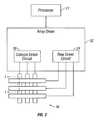
- FIG. 2is a system block diagram illustrating one embodiment of an electronic device incorporating a 3 ⁇ 3 interferometric modulator display.
- FIG. 3is a diagram of movable mirror position versus applied voltage for one exemplary embodiment of an interferometric modulator of FIG. 1 .
- FIG. 4is an illustration of a set of row and column voltages that may be used to drive an interferometric modulator display.
- FIGS. 5A and 5Billustrate one exemplary timing diagram for row and column signals that may be used to write a frame of display data to the 3 ⁇ 3 interferometric modulator display of FIG. 2 .
- FIGS. 6A and 6Bare system block diagrams illustrating an embodiment of a visual display device comprising a plurality of interferometric modulators.
- FIG. 7Ais a cross section of the device of FIG. 1 .
- FIG. 7Bis a cross section of an alternative embodiment of an interferometric modulator.
- FIG. 7Cis a cross section of another alternative embodiment of an interferometric modulator.
- FIG. 7Dis a cross section of yet another alternative embodiment of an interferometric modulator.
- FIG. 7Eis a cross section of an additional alternative embodiment of an interferometric modulator.
- FIG. 8is a flow diagram illustrating certain steps in an embodiment of a method of making an interferometric modulator.
- FIG. 9Ais a view depicting a portion of one embodiment of an interferometric modulator display.
- FIG. 9Bis a cross section of the device of FIG. 9A , taken along line 9 B- 9 B of FIG. 9A .
- FIG. 9Cis a cross section of the device of FIG. 9A , taken along line 9 C- 9 C of FIG. 9A .
- FIG. 10Ais a view depicting a portion of another embodiment of an interferometric modulator display, in which slots are provided in the columns at sub-pixel boundaries.
- FIG. 10Bis a cross section of the device of FIG. 10A , taken along line 10 B- 10 B of FIG. 10A .
- FIG. 10Cis a cross section of the device of FIG. 10A , taken along line 10 C- 10 C of FIG. 10A .
- FIG. 11is a perspective view of a portion of a display according to another embodiment.
- FIG. 12Ais a view depicting a portion of a further embodiment of an interferometric modulator display.
- FIG. 12Bis a view depicting a portion of a still further embodiment of an interferometric modulator display.
- FIG. 13is a flow diagram illustrating certain steps in another embodiment of a method of making an interferometric modulator.
- FIG. 14is a flow diagram illustrating certain steps in a further embodiment of a method of making an interferometric modulator.
- FIG. 15Ais a graph illustrating the hysteresis properties of an interferometric modulator.
- FIG. 15Bis a graph illustrating the hysteresis properties of an interferometric modulator having a slot in the boundary region of the movable reflective layer, according to one embodiment.
- the embodimentsmay be implemented in or associated with a variety of electronic devices such as, but not limited to, mobile telephones, wireless devices, personal data assistants (PDAs), hand-held or portable computers, GPS receivers/navigators, cameras, MP3 players, camcorders, game consoles, wrist watches, clocks, calculators, television monitors, flat panel displays, computer monitors, auto displays (e.g., odometer display, etc.), cockpit controls and/or displays, display of camera views (e.g., display of a rear view camera in a vehicle), electronic photographs, electronic billboards or signs, projectors, architectural structures, packaging, and aesthetic structures (e.g., display of images on a piece of jewelry).
- Electromechanical devices of similar structure to those described hereincan also be used in non-display applications such as in electronic switching devices.
- an interferometric modulator displayincludes an electrically conductive deformable layer arranged as substantially parallel strips or columns. In conjunction with row electrodes, the columns define a plurality of individually actuatable sub-pixels of the display. The columns are provided with crosswise slots disposed generally at the boundary regions of each sub-pixel.
- the crosswise slotscan have a length selected to minimize mechanical cross-talk between adjacent sub-pixels of a given column, while maintaining sufficient material connecting the adjacent sub-pixels so as not to significantly degrade the electrical characteristics (including conductivity and capacitance) of the adjacent sub-pixels or the material connecting them.
- a method of fabricating an electromechanical systems deviceinvolves forming a deformable layer having plurality of electrically isolated columns, with one or more crosswise slots in the columns at boundary areas between adjacent sub-pixels in the columns.
- FIG. 1One interferometric modulator display embodiment comprising an interferometric MEMS display element is illustrated in FIG. 1 .
- the pixelsare in either a bright or dark state.
- the display elementIn the bright (“relaxed” or “open”) state, the display element reflects a large portion of incident visible light to a user.
- the dark (“actuated” or “closed”) stateWhen in the dark (“actuated” or “closed”) state, the display element reflects little incident visible light to the user.
- the light reflectance properties of the “on” and “off” statesmay be reversed.
- MEMS pixelscan be configured to reflect predominantly at selected colors, allowing for a color display in addition to black and white.
- FIG. 1is an isometric view depicting two adjacent pixels in a series of pixels of a visual display, wherein each pixel comprises a MEMS interferometric modulator.
- an interferometric modulator displaycomprises a row/column array of these interferometric modulators.
- Each interferometric modulatorincludes a pair of reflective layers positioned at a variable and controllable distance from each other to form a resonant optical gap with at least one variable dimension.
- one of the reflective layersmay be moved between two positions. In the first position, referred to herein as the relaxed position, the movable reflective layer is positioned at a relatively large distance from a fixed partially reflective layer.
- the movable reflective layerIn the second position, referred to herein as the actuated position, the movable reflective layer is positioned more closely adjacent to the partially reflective layer. Incident light that reflects from the two layers interferes constructively or destructively depending on the position of the movable reflective layer, producing either an overall reflective or non-reflective state for each pixel.
- the depicted portion of the pixel array in FIG. 1includes two adjacent interferometric modulators 12 a and 12 b .
- a movable reflective layer 14 ais illustrated in a relaxed position at a predetermined distance from an optical stack 16 a , which includes a partially reflective layer.
- the movable reflective layer 14 bis illustrated in an actuated position adjacent to the optical stack 16 b.
- optical stack 16typically comprise several fused layers, which can include an electrode layer, such as indium tin oxide (ITO), a partially reflective layer, such as chromium, and a transparent dielectric.
- ITOindium tin oxide
- the optical stack 16is thus electrically conductive, partially transparent and partially reflective, and may be fabricated, for example, by depositing one or more of the above layers onto a transparent substrate 20 .
- the partially reflective layercan be formed from a variety of materials that are partially reflective such as various metals, semiconductors, and dielectrics.
- the partially reflective layercan be formed of one or more layers of materials, and each of the layers can be formed of a single material or a combination of materials.
- the layers of the optical stack 16are patterned into parallel strips, and may form row electrodes in a display device as described further below.
- the movable reflective layers 14 a , 14 bmay be formed as a series of parallel strips of a deposited metal layer or layers (orthogonal to the row electrodes of 16 a , 16 b ) to form columns deposited on top of posts 18 and an intervening sacrificial material deposited between the posts 18 . When the sacrificial material is etched away, the movable reflective layers 14 a , 14 b are separated from the optical stacks 16 a , 16 b by a defined gap 19 .
- a highly conductive and reflective material such as aluminummay be used for the reflective layers 14 , and these strips may form column electrodes in a display device. Note that FIG. 1 may not be to scale. In some embodiments, the spacing between posts 18 may be on the order of 10-100 um, while the gap 19 may be on the order of ⁇ 1000 Angstroms.
- the gap 19remains between the movable reflective layer 14 a and optical stack 16 a , with the movable reflective layer 14 a in a mechanically relaxed state, as illustrated by the pixel 12 a in FIG. 1 .
- a potential (voltage) differenceis applied to a selected row and column, the capacitor formed at the intersection of the row and column electrodes at the corresponding pixel becomes charged, and electrostatic forces pull the electrodes together. If the voltage is high enough, the movable reflective layer 14 is deformed and is forced against the optical stack 16 .
- a dielectric layerwithin the optical stack 16 may prevent shorting and control the separation distance between layers 14 and 16 , as illustrated by actuated pixel 12 b on the right in FIG. 1 . The behavior is the same regardless of the polarity of the applied potential difference.
- FIGS. 2 through 5illustrate one exemplary process and system for using an array of interferometric modulators in a display application.
- FIG. 2is a system block diagram illustrating one embodiment of an electronic device that may incorporate interferometric modulators.
- the electronic deviceincludes a processor 21 which may be any general purpose single- or multi-chip microprocessor such as an ARM®, Pentium®, 8051, MIPS®, Power PC®, or ALPHA®, or any special purpose microprocessor such as a digital signal processor, microcontroller, or a programmable gate array.
- the processor 21may be configured to execute one or more software modules.
- the processormay be configured to execute one or more software applications, including a web browser, a telephone application, an email program, or any other software application.
- the processor 21is also configured to communicate with an array driver 22 .
- the array driver 22includes a row driver circuit 24 and a column driver circuit 26 that provide signals to a display array or panel 30 .
- the cross section of the array illustrated in FIG. 1is shown by the lines 1 - 1 in FIG. 2 .
- FIG. 2illustrates a 3 ⁇ 3 array of interferometric modulators for the sake of clarity, the display array 30 may contain a very large number of interferometric modulators, and may have a different number of interferometric modulators in rows than in columns (e.g., 300 pixels per row by 190 pixels per column).
- FIG. 3is a diagram of movable mirror position versus applied voltage for one exemplary embodiment of an interferometric modulator of FIG. 1 .
- the row/column actuation protocolmay take advantage of a hysteresis property of these devices as illustrated in FIG. 3 .
- An interferometric modulatormay require, for example, a 10 volt potential difference to cause a movable layer to deform from the relaxed state to the actuated state. However, when the voltage is reduced from that value, the movable layer maintains its state as the voltage drops back below 10 volts. In the exemplary embodiment of FIG. 3 , the movable layer does not relax completely until the voltage drops below 2 volts.
- the row/column actuation protocolcan be designed such that during row strobing, pixels in the strobed row that are to be actuated are exposed to a voltage difference of about 10 volts, and pixels that are to be relaxed are exposed to a voltage difference of close to zero volts.
- each pixelsees a potential difference within the “stability window” of 3-7 volts in this example.
- This featuremakes the pixel design illustrated in FIG. 1 stable under the same applied voltage conditions in either an actuated or relaxed pre-existing state. Since each pixel of the interferometric modulator, whether in the actuated or relaxed state, is essentially a capacitor formed by the fixed and moving reflective layers, this stable state can be held at a voltage within the hysteresis window with almost no power dissipation. Essentially no current flows into the pixel if the applied potential is fixed.
- a frame of an imagemay be created by sending a set of data signals (each having a certain voltage level) across the set of column electrodes in accordance with the desired set of actuated pixels in the first row.
- a row pulseis then applied to a first row electrode, actuating the pixels corresponding to the set of data signals.
- the set of data signalsis then changed to correspond to the desired set of actuated pixels in a second row.
- a pulseis then applied to the second row electrode, actuating the appropriate pixels in the second row in accordance with the data signals.
- the first row of pixelsare unaffected by the second row pulse, and remain in the state they were set to during the first row pulse. This may be repeated for the entire series of rows in a sequential fashion to produce the frame.
- the framesare refreshed and/or updated with new image data by continually repeating this process at some desired number of frames per second.
- a wide variety of protocols for driving row and column electrodes of pixel arrays to produce image framesmay be used.
- FIGS. 4 and 5illustrate one possible actuation protocol for creating a display frame on the 3 ⁇ 3 array of FIG. 2 .
- FIG. 4illustrates a possible set of column and row voltage levels that may be used for pixels exhibiting the hysteresis curves of FIG. 3 .
- actuating a pixelinvolves setting the appropriate column to ⁇ Vbias, and the appropriate row to + ⁇ V, which may correspond to ⁇ 5 volts and +5 volts respectively Relaxing the pixel is accomplished by setting the appropriate column to +Vbias, and the appropriate row to the same + ⁇ V, producing a zero volt potential difference across the pixel.
- the pixelsare stable in whatever state they were originally in, regardless of whether the column is at +Vbias, or ⁇ Vbias.
- voltages of opposite polarity than those described abovecan be used, e.g., actuating a pixel can involve setting the appropriate column to +Vbias, and the appropriate row to ⁇ V.
- releasing the pixelis accomplished by setting the appropriate column to ⁇ Vbias, and the appropriate row to the same ⁇ V, producing a zero volt potential difference across the pixel.
- FIG. 5Bis a timing diagram showing a series of row and column signals applied to the 3 ⁇ 3 array of FIG. 2 which will result in the display arrangement illustrated in FIG. 5A , where actuated pixels are non-reflective.
- the pixelsPrior to writing the frame illustrated in FIG. 5A , the pixels can be in any state, and in this example, all the rows are initially at 0 volts, and all the columns are at +5 volts. With these applied voltages, all pixels are stable in their existing actuated or relaxed states.
- pixels ( 1 , 1 ), ( 1 , 2 ), ( 2 , 2 ), ( 3 , 2 ) and ( 3 , 3 )are actuated.
- columns 1 and 2are set to ⁇ 5 volts
- column 3is set to +5 volts. This does not change the state of any pixels, because all the pixels remain in the 3-7 volt stability window.
- Row 1is then strobed with a pulse that goes from 0, up to 5 volts, and back to zero. This actuates the ( 1 , 1 ) and ( 1 , 2 ) pixels and relaxes the ( 1 , 3 ) pixel. No other pixels in the array are affected.
- row 2is set to ⁇ 5 volts, and columns 1 and 3 are set to +5 volts.
- the same strobe applied to row 2will then actuate pixel ( 2 , 2 ) and relax pixels ( 2 , 1 ) and ( 2 , 3 ). Again, no other pixels of the array are affected.
- Row 3is similarly set by setting columns 2 and 3 to ⁇ 5 volts, and column 1 to +5 volts.
- the row 3strobe sets the row 3 pixels as shown in FIG. 5A . After writing the frame, the row potentials are zero, and the column potentials can remain at either +5 or ⁇ 5 volts, and the display is then stable in the arrangement of FIG. 5A .
- FIGS. 6A and 6Bare system block diagrams illustrating an embodiment of a display device 40 .
- the display device 40can be, for example, a cellular or mobile telephone.
- the same components of display device 40 or slight variations thereofare also illustrative of various types of display devices such as televisions and portable media players.
- the display device 40includes a housing 41 , a display 30 , an antenna 43 , a speaker 45 , an input device 48 , and a microphone 46 .
- the housing 41is generally formed from any of a variety of manufacturing processes, including injection molding, and vacuum forming.
- the housing 41may be made from any of a variety of materials, including but not limited to plastic, metal, glass, rubber, and ceramic, or a combination thereof.
- the housing 41includes removable portions (not shown) that may be interchanged with other removable portions of different color, or containing different logos, pictures, or symbols.
- the display 30 of exemplary display device 40may be any of a variety of displays, including a bi-stable display, as described herein.
- the display 30includes a flat-panel display, such as plasma, EL, OLED, STN LCD, or TFT LCD as described above, or a non-flat-panel display, such as a CRT or other tube device.
- the display 30includes an interferometric modulator display, as described herein.
- the components of one embodiment of exemplary display device 40are schematically illustrated in FIG. 6B .
- the illustrated exemplary display device 40includes a housing 41 and can include additional components at least partially enclosed therein.
- the exemplary display device 40includes a network interface 27 that includes an antenna 43 which is coupled to a transceiver 47 .
- the transceiver 47is connected to a processor 21 , which is connected to conditioning hardware 52 .
- the conditioning hardware 52may be configured to condition a signal (e.g. filter a signal).
- the conditioning hardware 52is connected to a speaker 45 and a microphone 46 .
- the processor 21is also connected to an input device 48 and a driver controller 29 .
- the driver controller 29is coupled to a frame buffer 28 , and to an array driver 22 , which in turn is coupled to a display array 30 .
- a power supply 50provides power to all components as required by the particular exemplary display device 40 design.
- the network interface 27includes the antenna 43 and the transceiver 47 so that the exemplary display device 40 can communicate with one ore more devices over a network. In one embodiment the network interface 27 may also have some processing capabilities to relieve requirements of the processor 21 .
- the antenna 43is any antenna for transmitting and receiving signals. In one embodiment, the antenna transmits and receives RF signals according to the IEEE 802.11 standard, including IEEE 802.11(a), (b), or (g). In another embodiment, the antenna transmits and receives RF signals according to the BLUETOOTH standard. In the case of a cellular telephone, the antenna is designed to receive CDMA, GSM, AMPS, W-CDMA, or other known signals that are used to communicate within a wireless cell phone network.
- the transceiver 47pre-processes the signals received from the antenna 43 so that they may be received by and further manipulated by the processor 21 .
- the transceiver 47also processes signals received from the processor 21 so that they may be transmitted from the exemplary display device 40 via the antenna 43 .
- the transceiver 47can be replaced by a receiver.
- network interface 27can be replaced by an image source, which can store or generate image data to be sent to the processor 21 .
- the image sourcecan be a digital video disc (DVD) or a hard-disc drive that contains image data, or a software module that generates image data.
- Processor 21generally controls the overall operation of the exemplary display device 40 .
- the processor 21receives data, such as compressed image data from the network interface 27 or an image source, and processes the data into raw image data or into a format that is readily processed into raw image data.
- the processor 21then sends the processed data to the driver controller 29 or to frame buffer 28 for storage.
- Raw datatypically refers to the information that identifies the image characteristics at each location within an image. For example, such image characteristics can include color, saturation, and gray-scale level.
- the processor 21includes a microcontroller, CPU, or logic unit to control operation of the exemplary display device 40 .
- Conditioning hardware 52generally includes amplifiers and filters for transmitting signals to the speaker 45 , and for receiving signals from the microphone 46 .
- Conditioning hardware 52may be discrete components within the exemplary display device 40 , or may be incorporated within the processor 21 or other components.
- the driver controller 29takes the raw image data generated by the processor 21 either directly from the processor 21 or from the frame buffer 28 and reformats the raw image data appropriately for high speed transmission to the array driver 22 . Specifically, the driver controller 29 reformats the raw image data into a data flow having a raster-like format, such that it has a time order suitable for scanning across the display array 30 . Then the driver controller 29 sends the formatted information to the array driver 22 .
- a driver controller 29such as a LCD controller, is often associated with the system processor 21 as a stand-alone Integrated Circuit (IC), such controllers may be implemented in many ways. They may be embedded in the processor 21 as hardware, embedded in the processor 21 as software, or fully integrated in hardware with the array driver 22 .
- the array driver 22receives the formatted information from the driver controller 29 and reformats the video data into a parallel set of waveforms that are applied many times per second to the hundreds and sometimes thousands of leads coming from the display's x-y matrix of pixels.
- driver controller 29is a conventional display controller or a bi-stable display controller (e.g., an interferometric modulator controller).
- array driver 22is a conventional driver or a bi-stable display driver (e.g., an interferometric modulator display).
- a driver controller 29is integrated with the array driver 22 .
- display array 30is a typical display array or a bi-stable display array (e.g., a display including an array of interferometric modulators).
- the input device 48allows a user to control the operation of the exemplary display device 40 .
- input device 48includes a keypad, such as a QWERTY keyboard or a telephone keypad, a button, a switch, a touch-sensitive screen, a pressure- or heat-sensitive membrane.
- the microphone 46is an input device for the exemplary display device 40 . When the microphone 46 is used to input data to the device, voice commands may be provided by a user for controlling operations of the exemplary display device 40 .
- Power supply 50can include a variety of energy storage devices as are well known in the art.
- power supply 50is a rechargeable battery, such as a nickel-cadmium battery or a lithium ion battery.
- power supply 50is a renewable energy source, a capacitor, or a solar cell, including a plastic solar cell, and solar-cell paint.
- power supply 50is configured to receive power from a wall outlet.
- control programmabilityresides, as described above, in a driver controller which can be located in several places in the electronic display system. In some cases control programmability resides in the array driver 22 .
- the above-described optimizationmay be implemented in any number of hardware and/or software components and in various configurations.
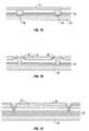
- FIGS. 7A-7Eillustrate five different embodiments of the movable reflective layer 14 and its supporting structures.
- FIG. 7Ais a cross section of the embodiment of FIG. 1 , where a strip of metal material 14 is deposited on orthogonally extending supports 18 .
- the moveable reflective layer 14 of each interferometric modulatoris square or rectangular in shape and attached to supports at the corners only, on tethers 32 .
- the moveable reflective layer 14is square or rectangular in shape and suspended from a deformable layer 34 , which may comprise a flexible metal.
- the deformable layer 34connects, directly or indirectly, to the substrate 20 around the perimeter of the deformable layer 34 . These connections are herein referred to as support posts.
- the embodiment illustrated in FIG. 7Dhas support post plugs 42 upon which the deformable layer 34 rests.
- the movable reflective layer 14remains suspended over the gap, as in FIGS. 7A-7C , but the deformable layer 34 does not form the support posts by filling holes between the deformable layer 34 and the optical stack 16 . Rather, the support posts are formed of a planarization material, which is used to form support post plugs 42 .
- the embodiment illustrated in FIG. 7Eis based on the embodiment shown in FIG. 7D , but may also be adapted to work with any of the embodiments illustrated in FIGS.
- FIG. 7Ean extra layer of metal or other conductive material has been used to form a bus structure 44 . This allows signal routing along the back of the interferometric modulators, eliminating a number of electrodes that may otherwise have had to be formed on the substrate 20 .
- the interferometric modulatorsfunction as direct-view devices, in which images are viewed from the front side of the transparent substrate 20 , the side opposite to that upon which the modulator is arranged.
- the reflective layer 14optically shields the portions of the interferometric modulator on the side of the reflective layer opposite the substrate 20 , including the deformable layer 34 . This allows the shielded areas to be configured and operated upon without negatively affecting the image quality. For example, such shielding allows the bus structure 44 in FIG. 7E , which provides the ability to separate the optical properties of the modulator from the electromechanical properties of the modulator, such as addressing and the movements that result from that addressing.
- This separable modulator architectureallows the structural design and materials used for the electromechanical aspects and the optical aspects of the modulator to be selected and to function independently of each other.
- the embodiments shown in FIGS. 7C-7Ehave additional benefits deriving from the decoupling of the optical properties of the reflective layer 14 from its mechanical properties, which are carried out by the deformable layer 34 .
- Thisallows the structural design and materials used for the reflective layer 14 to be optimized with respect to the optical properties, and the structural design and materials used for the deformable layer 34 to be optimized with respect to desired mechanical properties.
- FIG. 8illustrates certain steps in an embodiment of a manufacturing process 800 for an optical modulator, such as an interferometric modulator. Such steps may be present in a process for manufacturing, e.g., interferometric modulators of the general type illustrated in FIGS. 1 and 7 , along with other steps not shown in FIG. 8 .
- the process 800begins at step 805 with the formation of the optical stack 16 over the substrate 20 .
- the substrate 20may be a transparent substrate such as glass or plastic and may have been subjected to prior preparation step(s), e.g., cleaning, to facilitate efficient formation of the optical stack 16 .
- the optical stack 16is electrically conductive, partially transparent and partially reflective, and may be fabricated, for example, by depositing one or more of the layers onto the transparent substrate 20 .
- the layersare patterned into parallel strips, and may form row electrodes in a display device.
- the term “patterned”is used herein to refer to patterning as well as etching processes.
- the optical stack 16includes an insulating or dielectric layer that is deposited over one or more metal layers (e.g., reflective and/or conductive layers).
- the process 800 illustrated in FIG. 8continues at step 810 with the formation of a sacrificial layer over the optical stack 16 .
- the sacrificial layeris later removed (e.g., at step 825 ) to form the cavity 19 as discussed below and thus the sacrificial layer is not shown in the resulting interferometric modulator 12 illustrated in FIG. 1 .
- the formation of the sacrificial layer over the optical stack 16may include deposition of a XeF 2 -etchable material such as molybdenum or amorphous silicon, in a thickness selected to provide, after subsequent removal, a cavity 19 having the desired size.
- Deposition of the sacrificial materialmay be carried out using deposition techniques such as physical vapor deposition (PVD, e.g., sputtering), plasma-enhanced chemical vapor deposition (PECVD), thermal chemical vapor deposition (thermal CVD), or spin-coating.
- PVDphysical vapor deposition
- PECVDplasma-enhanced chemical vapor deposition
- thermal CVDthermal chemical vapor deposition
- spin-coatingspin-coating.
- the process 800 illustrated in FIG. 8continues at step 815 with the formation of a support structure e.g., a post 18 as illustrated in FIGS. 1 and 7 .
- the formation of the post 18may include the steps of patterning the sacrificial layer to form a support structure aperture, then depositing a material (e.g., a polymer or a silicon oxide) into the aperture to form the post 18 , using a deposition method such as PECVD, thermal CVD, or spin-coating.
- a materiale.g., a polymer or a silicon oxide
- the support structure aperture formed in the sacrificial layerextends through both the sacrificial layer and the optical stack 16 to the underlying substrate 20 , so that the lower end of the post 18 contacts the substrate 20 as illustrated in FIG. 7A .
- the aperture formed in the sacrificial layerextends through the sacrificial layer, but not through the optical stack 16 .
- FIG. 7Dillustrates the lower end of the support post plugs 42 in contact with the optical stack 16 .
- the process 800 illustrated in FIG. 8continues at step 820 with the formation of a movable reflective layer or membrane such as the movable reflective layer 14 illustrated in FIGS. 1 and 7 .
- the movable reflective layer 14may be formed by employing one or more deposition steps, e.g., reflective layer (e.g., aluminum, aluminum alloy) deposition, along with one or more patterning, masking, and/or etching steps.
- the movable reflective layer 14is typically electrically conductive, and may be referred to herein as an electrically conductive layer. Since the sacrificial layer is still present in the partially fabricated interferometric modulator formed at step 820 of the process 800 , the movable reflective layer 14 is typically not movable at this stage.
- a partially fabricated interferometric modulator that contains a sacrificial layermay be referred to herein as an “unreleased” interferometric modulator.
- the process 800 illustrated in FIG. 8continues at step 825 with the formation of a cavity, e.g., a cavity 19 as illustrated in FIGS. 1 and 7 .
- the cavity 19may be formed by exposing the sacrificial material (deposited at step 810 ) to an etchant.
- an etchable sacrificial materialsuch as molybdenum or amorphous silicon may be removed by dry chemical etching, e.g., by exposing the sacrificial layer to a gaseous or vaporous etchant, such as vapors derived from solid xenon difluoride (XeF 2 ) for a period of time that is effective to remove the desired amount of material, typically selectively relative to the structures surrounding the cavity 19 .
- a gaseous or vaporous etchantsuch as vapors derived from solid xenon difluoride (XeF 2 )
- Other etching methodse.g. wet etching and/or plasma etching, may also be used. Since the sacrificial layer is removed during step 825 of the process 800 , the movable reflective layer 14 is typically movable after this stage. After removal of the sacrificial material, the resulting fully or partially fabricated interferometric modulator may be referred to here
- a MEMS displaycan comprise one or more pixels that each comprise a plurality of sub-pixels.
- Each sub-pixelcan comprise an independently movable and/or independently actuatable optical modulator.
- a single pixelcan be configured to reflect multiple colors, depending on the particular configuration of the individual sub-pixels and the selection of sub-pixels that are actuated.
- a MEMS displaycan be configured with pixels that are divided into nine sub-pixels, with three sub-pixels in a column configured to reflect blue light, three sub-pixels in an adjacent column configured to reflect green light, and three sub-pixels in the next column configured to reflect red light in their unactuated (relaxed) states.
- the modulators in the columns of a given pixelcan have differently sized air gaps and/or different thicknesses. In such an example, individually actuating different combinations of sub-pixels causes the pixel to reflect different colors.
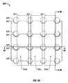
- FIG. 9Ais a view depicting a portion of one embodiment of an interferometric modulator display 900 that includes three parallel row electrodes 902 and three strips 904 of a deformable (or otherwise movable) reflective layer, arranged in columns extending perpendicular to the row electrodes 902 .
- the overlapping portions of the row electrodes 902 and the column electrodes 904define nine sub-pixels 906 (comprising three each of sub-pixels 906 a , 906 b , and 906 c ).
- Supports 908are disposed at corner regions of each sub-pixel, on or near border regions of the row electrodes 902 , and are configured to support edge portions of the column electrodes 904 .
- row electrodescan be electrically conductive portions of the optical stack.
- reference to row electrodes in this and the following discussionwill be understood as a reference to the electrically conductive metal layer(s) (e.g., ITO) of an optical stack, such as the optical stack 16 illustrated in FIGS. 7A-7E .
- ITOelectrically conductive metal layer
- Column electrodescan comprise one or more layers which can be light-reflective and electrically conductive, and can be movable towards the optical stack.
- FIG. 9Bshows a cross-section of a portion of the display 900 illustrated in FIG. 9A , and also shows a substrate 910 underlying the optical stack, which includes row electrodes 902 , a partially reflective and partially transmissive layer 903 , and dielectric layers 912 a , 912 b .
- optical mask structures 909underlying the supports 908 .
- the optical mask structures 909also referred to as “black mask” structures, can be configured to absorb ambient or stray light and to improve the optical response of a display device by increasing the contrast ratio. In some applications, the optical mask can reflect light of a predetermined wavelength to appear as a color other than black.
- the optical mask structurescan also be conductive, and thus can be configured to function as an electrical bussing layer.
- the conductive bus structurescan be configured with a lower electrical resistance than the row and/or column electrodes themselves, to improve the response time of the sub-pixels in an array.
- a conductive bus structurecan also be provided separately from the optical mask structure.
- a conductive mask or other conductive bus structurecan be electrically coupled to one or more of the elements on the display to provide one or more electrical paths for voltages applied to one or more of the display elements.
- one or more of the row or column electrodescan be connected to the conductive bus structure to reduce the resistance of the connected row or column electrode.
- the conductive bus structurescan be connected to the row electrodes 902 through one or more vias (not shown in FIG. 9B ), which can be disposed underneath the supports 908 or in any other suitable location.
- the column electrodes 904can comprise multiple layers.
- the column electrode 904 illustrated in FIG. 9Bcomprises a reflective layer 904 a and a flexible layer 904 b .
- the flexible layer 904 bcan be formed directly over and/or in continuous contact with the reflective layer 904 a .
- the flexible layer 904 bcan comprise a dielectric material, a conductive material, or any other suitable material.
- the reflective layer 904 acomprises aluminum.
- the columns 904 of a given pixelcan have different thicknesses, and/or multiple layers of the same or different thicknesses.
- the column electrode 904 of sub-pixel 906 acan comprise a single reflective layer 904 a and a single flexible supporting layer 904 b .
- the column electrode 904 of sub-pixel 906 bcan an additional supporting layer 904 c to increase the stiffness of the sub-pixel 906 b relative to sub-pixel 906 a .
- the column electrode 904 of sub-pixel 906 ccan have yet another supporting layer 904 d in order to increase the stiffness of the sub-pixel 906 c relative to sub-pixel 906 b .
- the various supporting layers 904 b , 904 c , and 904 dcan comprise the same or different material, and can have the same or different thicknesses as required by the particular application.
- the sub-pixels in a displaycan be configured with differently sized air gaps between their columns and optical stacks. For example, as shown in FIG. 9C , sub-pixel 906 a is configured with the relatively largest air gap in the illustrated display, sub-pixel 906 b has a somewhat smaller air gap, and sub-pixel 906 c is configured with the relatively smallest air gap in the illustrated display.
- the sub-pixels in a displaycan be configured to reflect various desired colors at similar actuation voltages.
- the interferometric modulator display 900can be manufactured using the method 800 of FIG. 8 .
- the row electrodes 902can be formed at the step 805 as part of the optical stack.
- the row electrodes 902can be formed in any suitable fashion, for example, they can be formed as a single layer which is then patterned and etched to separate and electrically isolate the rows 902 from one another.
- the supports 908can be formed within apertures formed within the sacrificial layer in a region along the periphery of each sub-pixel to support edge portions of the columns 904 of the deformable reflective layer or membrane.
- the parallel strips 904 of the movable reflective layercan be formed at step 820 .
- the parallel strips 904can be formed over the sacrificial layer and the supports 908 so as to be supported when the sacrificial layer is removed at step 825 .
- the parallel strips 904can be initially formed as a single layer which is then patterned and etched to separate and, thus, physically and electrically isolate the column electrodes 904 from one another.
- MEMS displays having the general configuration shown in FIGS. 9A , 9 B, and 9 Ccan exhibit undesirable mechanical cross-talk between adjacent sub-pixels within each column; that is, the state of a particular sub-pixel may be affected by the state of its neighboring sub-pixel(s), resulting in unintended deflection in either or both sub-pixels, which deteriorates the optical performance of either or both sub-pixels.
- MEMS displays having the general configuration shown in FIG. 9have exhibited undesirable soft release issues; that is, the various edges of an individual sub-pixel may not release from an actuated state all at once, but may instead release at different release voltages, resulting in a smaller useable hysteresis window.
- the edges of the sub-pixel which are closest to the adjacent sub-pixels in the same columnmay release at a lower voltage than its other two edges.
- the cross-talk and soft release issues exhibited in configurations such as thesemay be due to varying stiffness of the deformable layer in the row and column directions.
- creating crosswise slots in the columns at or near the sub-pixel boundariescan facilitate independent movement of neighboring sub-pixel regions of the movable reflective layer, thereby reducing mechanical cross-talk between sub-pixels.
- creating crosswise slots in the columnsimproves uniformity of stress states around the edges of a sub-pixel, and therefore promotes simultaneous release of the edges of a sub-pixel.
- the crosswise slotscan thus reduce soft release problems and increase the useable hysteresis window of the display.
- creating crosswise slots in the columncan also improve the uniformity of reflected color across a sub-pixel.
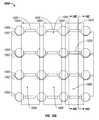
- FIG. 10Ais a view depicting a portion of one embodiment of an interferometric modulator display 1000 that includes three parallel row electrodes 1002 and three strips 1004 of a deformable reflective layer, arranged in columns extending perpendicular to the row electrodes 1002 .
- the overlapping portions of the row electrodes 1002 and the columns 1004define nine sub-pixels 1006 .
- the row electrodes 1002 and the columns 1004can extend in both longitudinal and lateral directions to connect multiple pixels in an array.
- supports 1008are disposed at corner regions of each sub-pixel, on or near border regions of the row electrodes 1002 .
- the supports 1008are configured to support edge portions of the columns 1004 .
- the supports 1008can have a generally octagonal-shaped cross-section, as shown in the figure. Alternatively, the supports 1008 can have any other suitably-shaped cross section, for example, circular, oval, rectangular, diamond-shaped, or square.
- openings or slots 1020are provided in each of the columns 1004 .
- the crosswise slots 1020can have a width (or first) dimension and a length (or second) dimension, the length dimension greater than their width dimension, and be formed such that the length dimension can extend in a direction generally perpendicular to the direction in which the columns 1004 extend. In some embodiments the length dimension extends substantially or exactly perpendicular to the direction in which the columns 1004 extend.
- the slots 1020can be created in the boundary regions between adjacent sub-pixels of a given column 1004 , generally between each pair of supports 1008 that support the edges of the column 1004 .
- the slots 1020can comprise generally elongate openings extending between the two edges of a particular column 1004 .
- the slots 1020can be generally rectangular, generally oblong, or can have any other suitable configuration for their intended purpose.
- the slots 1020can have a length selected to substantially eliminate mechanical cross-talk between adjacent sub-pixels in the column 1004 , while leaving a sufficient amount of material connecting the adjacent sub-pixels so as not to degrade the electrical characteristics of the display (such as, for example, conductivity or capacitance of the column 1004 ).
- the slots 1020can have a width substantially similar to the lateral spacing between the columns 1004 , or can have any other width consistent with their intended purpose.
- the slots 1020are created in a central (or middle) region between parallel edges of the column 1004 , leaving material of the deformable layer extending along the edges of the column 1004 at both ends of the slots 1020 .
- FIGS. 10B and 10Cshow different cross-sections through the display 1000 illustrated in FIG. 10A .
- FIGS. 10B and 10Cadditionally show a substrate 1010 underlying the optical stack, which includes row electrodes 1002 , a partially reflective and partially transmissive layer 1003 , and dielectric layers 1012 a , 1012 b .
- FIG. 10Bis taken through an edge portion of the column 1004 , away from the slots 1020 .
- the column 1004has a multi-layer structure that includes a reflective layer 1004 a and a flexible supporting layer 1004 b .
- the material comprising the column 1004(including the layers 1004 a , 1004 b ) is continuous through the illustrated portion.
- the material comprising the column 1004(including the layers 1004 a , 1004 b ) is discontinuous through the illustrated portion at locations near the supports 1008 .
- FIG. 11is a perspective view illustrating a display 1100 according to another embodiment, comprising row electrodes 1102 and electrically conductive, deformable columns 1104 defining a number of sub-pixels 1106 .
- Supports 1108are disposed generally between the row electrodes 1102 and the columns 1104 .
- the illustrated supports 1108have a generally rectangular-shaped cross section.
- a plurality of crosswise slots 1120are provided in each of the columns 1104 to at least partially mechanically separate the adjacent sub-pixels 1106 in each column 1104 , while maintaining an adequate electrical connection through the column 1104 .
- the slots 1120can be disposed about centrally between the supports 1108 , so as to leave about an equal amount of material in the deformable layer connecting the adjacent sub-pixels 1106 on either end of the slots 1120 . This may help maintain consistent electrical properties (e.g., impedance) throughout the deformable layer. However, in some embodiments, the slots can be placed off-center so as to leave a different amount of material in the deformable layer between each end of the slot and each edge of the column.
- FIG. 12Ais a top plan view illustrating a display 1200 according to another embodiment, comprising row electrodes 1202 and electrically conductive, deformable columns 1204 defining a number of sub-pixels 1206 .
- Supports 1208are disposed generally between the row electrodes 1202 and the columns 1204 .
- a plurality of crosswise slots 1220are provided in each of the columns 1204 to at least partially mechanically separate the adjacent sub-pixels 1206 in each column 1204 , while maintaining an adequate electrical connection through the column 1204 .
- FIG. 12Ais a top plan view illustrating a display 1200 according to another embodiment, comprising row electrodes 1202 and electrically conductive, deformable columns 1204 defining a number of sub-pixels 1206 .
- Supports 1208are disposed generally between the row electrodes 1202 and the columns 1204 .
- a plurality of crosswise slots 1220are provided in each of the columns 1204 to at least partially mechanically separate the adjacent sub-pixels 1206 in each column 120
- the slots 1220have a length which extends approximately from an edge 1212 of a first support 1208 to an edge 1214 of a second support 1208 , thereby leaving a connecting portion of the deformable column 1204 over each support 1208 (between the ends of the slots 1220 and the edges of the column 1204 ) to connect the deformable column between each sub-pixel 1206 .
- the slotscan have a length slightly greater than a distance between two of the supports 1220 —that is, the slots can be dimensioned such that the ends of the slots 1220 extend slightly over the edges 1212 , 1214 of two adjacent supports 1208 .
- the slots 1220can be dimensioned so as to maximize the mechanical separation of adjacent sub-pixels 1206 in each column 1204 , while avoiding potential problems that may result if too narrow a strip of material remains along the edges of the column 1204 . Such problems can include the possibility of complete discontinuity in the mechanical layer due to process variation, as well as increased resistance of the column 1204 .
- the slotscan be dimensioned so as to leave about 2 ⁇ m of material between each end of the slot 1220 and the edges of the column 1204 .
- the slotscan be dimensioned so as to leave more than about 2 ⁇ m of material between each end of the slot 1220 and the edges of the column 1204 ; for example, the slots can be dimensioned to leave about 3 ⁇ m of material between each end of the slot 1220 and the edges of the column.
- the supportsare configured so as to effect generally the same stiffness in the movable layer across both column and slot directions of a sub-pixel.
- the sub-pixel shapeis a square which has generally the same length in both the column and slot directions.
- the support postscan have a generally symmetrical configuration in both the column and slot directions. Examples of such shapes include square, octagonal, and circular shapes.
- the sub-pixel shapeis a rectangle which has a longer length along one direction than the other direction.
- the support postscan be configured with dimensions which vary across the two directions. Examples of such shapes include rectangular and oblong shapes. Depending on the pixel arrangement, square and diamond posts are also possible.
- the shape of the support postscan also be selected with process considerations in mind.
- the postcan be rectangular shape with its longer dimension extending in the direction of the slots.
- the length of the slotcan be relatively smaller, leaving relatively more material connecting adjacent sub-pixels in the same column.
- a plurality of openingscan be provided at each boundary region between adjacent sub-pixels in order to decrease the mechanical connection between the adjacent sub-pixels.
- a series of perforations or holes(two, three, or more) can be created in the deformable layer between two supports supporting either edge of the column.
- the holesmay be circular, or oblong, in some embodiments.
- the seriescan extend in a generally perpendicular direction to the direction in which the columns extend.
- FIG. 12Bshows a display 1201 according to an embodiment.
- the display 1201includes generally the same features as display 1200 of FIG. 12A , including row electrodes 1202 and electrically conductive, deformable columns 1204 defining a number of sub-pixels 1206 .
- a series of holes 1221are provided at the boundary regions between adjacent sub-pixels 1206 .
- Each series of holes 1221has a length greater than the width of the holes 1221 , and thus forms a slot extending generally perpendicular to the direction in which the columns 1204 extend.
- Each series of holes 1221can extend generally between the edges 1212 , 1214 of adjacent supports 1208 , in order to partially mechanically separate the adjacent sub-pixels and improve the performance of the display 1201 .
- Adding crosswise slots at the boundary regions between adjacent sub-pixels in a columncan serve to make the entire sub-pixel structure more symmetric, which results in balanced stiffness among both the lengthwise and crosswise edges of the sub-pixel (that is, among the edges separating the individual columns and the edges near the slots).
- Such a configurationcan reduce sub-pixel soft release problems and significantly increase the useable hysteresis window.
- the slotshave the additional advantage of facilitating faster air flow through the deformable layer during sub-pixel actuation, thereby serving to reduce potential damping cross-talk and increase sub-pixel response time for fast actuation.
- adding slots as described hereincan provide these and other benefits without additional masks, process steps or fabrication cost.
- the crosswise slotscan be easily implemented during fabrication of the display, for example during the same process step in which mechanical cuts are made in the deformable layer to create the columns.
- the crosswise slotscan be formed in the deformable layer at step 820 of the process 800 .
- the process 1300begins at step 1302 with providing a substrate.
- the substratemay be a transparent substrate such as glass or plastic, or a non-transparent substrate such as silicon, and may have been subjected to prior preparation step(s), e.g., cleaning, to facilitate efficient formation of an optical stack as described elsewhere herein.
- the process 1300 illustrated in FIG. 13continues at step 1304 with the formation of a movable structure over the substrate.
- the movable structurecan include a reflective layer and at least one deformable layer, such as the reflective layer 1004 a and the deformable layer 1004 b illustrated in FIG. 10B .
- the reflective layercan be formed so as to be in substantially continuous contact with the deformable layer.
- the movable structurecan be electrically conductive, and can be spaced apart from the substrate by one or more support structures, such as the supports 1008 illustrated in FIG. 10B .
- the supportscan be formed or placed over the substrate in any suitable fashion, and can have any suitable configuration consistent with their intended purpose.
- step 1306The process 1300 illustrated in FIG. 13 then moves to step 1306 , during which electrically isolated columns are formed in the movable structure.
- step 1308one or more crosswise slots are created in one or more of the columns. Creating the slots can involve patterning and etching the columns so as to partially physically separate adjacent sub-portions within each column.
- the slots created at step 1308can extend in a generally crosswise direction in the columns; that is, in a generally perpendicular direction to the direction in which the columns extend.
- steps 1306 and 1308can be implemented at the same time, for example using the same mask. In other embodiments, steps 1306 and 1308 can be implemented sequentially.
- the MEMS device resulting from such a processcan be an optical modulator, such as an interferometric modulator.
- the process 1400begins at step 1402 with the formation of an optical stack over a substrate.
- the substratecan be a transparent substrate such as glass or plastic and may have been subjected to prior preparation step(s), e.g., cleaning, to facilitate efficient formation of the optical stack.
- the optical stackis electrically conductive, partially transparent and partially reflective, and may be fabricated, for example, by depositing one or more of the layers onto the transparent substrate.
- the layersare patterned to form parallel strips, and may form row electrodes in a display device.
- the optical stackincludes an insulating or dielectric layer that is deposited over one or more metal layers (e.g., reflective and/or conductive layers).
- the process 1400 illustrated in FIG. 14continues at step 1404 with the formation of a sacrificial layer over the optical stack.
- the sacrificial layeris later removed to form the cavity as discussed herein, and thus the sacrificial layer is not shown in some of the interferometric modulators illustrated in FIGS. 10 and 12 , for example.
- the formation of the sacrificial layer over the optical stackmay include deposition of a XeF 2 -etchable material such as molybdenum or amorphous silicon, in a thickness selected to provide, after subsequent removal, a cavity having the desired size.
- Deposition of the sacrificial materialmay be carried out using deposition techniques such as physical vapor deposition (PVD, e.g., sputtering), plasma-enhanced chemical vapor deposition (PECVD), thermal chemical vapor deposition (thermal CVD), or spin-coating.
- PVDphysical vapor deposition
- PECVDplasma-enhanced chemical vapor deposition
- thermal CVDthermal chemical vapor deposition
- spin-coatingspin-coating.
- the process 1400 illustrated in FIG. 14continues at step 1406 with the formation of a support structure e.g., a support 1008 as illustrated in FIG. 10 .
- the formation of the support 1008may include the steps of patterning the sacrificial layer to form a support structure aperture, then depositing a material (e.g., a polymer or a silicon oxide) into the aperture to form the support, using a deposition method such as PECVD, thermal CVD, or spin-coating.
- a materiale.g., a polymer or a silicon oxide
- the support structure aperture formed in the sacrificial layerextends through both the sacrificial layer and the optical stack to the underlying substrate, so that the lower end of the post contacts the substrate as illustrated in FIG. 7A .
- the aperture formed in the sacrificial layerextends through t the sacrificial layer, but not through the optical stack.
- FIG. 7Dillustrates the lower end of the support post plugs 42 in contact with the optical stack 16 .
- the process 1400 illustrated in FIG. 14continues at step 1408 with the formation of a movable reflective layer or membrane such as the electrically conductive deformable layer illustrated in FIGS. 1 and 7A .
- the movable reflective layermay be formed by employing one or more deposition steps, e.g., reflective layer (e.g., aluminum, aluminum alloy) deposition, along with one or more patterning, masking, and/or etching steps. Since the sacrificial layer is still present in the partially fabricated interferometric modulator formed at step 1408 of the process 1400 , the movable reflective layer may not be deformable or otherwise movable at this stage.
- step 1410with the formation of columns in the movable reflective layer.
- This stepcan involve removal of one or more portions of the movable reflective layer to form physically and electrically separated columns, such as the columns 1004 illustrated in FIG. 10 , which extend in a generally perpendicular direction to the row electrodes formed in step 1402 .
- the overlapping regions of the columns and rowsform sub-pixels of the device.
- the process 1400then moves to step 1412 , during which crosswise slots are formed in each column at the boundaries of the sub-pixels within each column.
- the slotscan be created in center regions of each column, so as to leave a strip of continuous material running along both edges of each column.
- steps 1410 and 1412are performed simultaneously, for example using the same mask. In other embodiments, the steps 1410 and 1412 can also be performed sequentially.
- FIGS. 15A and 15Bshow graphs illustrating the hysteresis properties of an interferometric modulator without slots ( FIG. 15A ) and of an interferometric modulator configured (e.g., with a slot) in accordance with an embodiment ( FIG. 15B ).
- the interferometric modulator configured according to an embodiment ( FIG. 15B )exhibits a wider hysteresis window, and thus possesses a larger usable operating voltage window, than does the modulator without a slot ( FIG. 15A ).
- the modulator without a slotexhibits soft release issues. In contrast, release is sharp in the interferometric modulator configured according to an embodiment ( FIG. 15B ).
- a MEMS displaywas configured with interferometric modulators having variously sized air gaps between the optical stack and the deformable layer, with the deformable layer arranged as parallel strips or columns. No slots were provided in the boundary regions between adjacent sub-pixels of each column.
- the modulatorsexhibited the following characteristics:
- a MEMS displaywas configured with interferometric modulators having variously sized air gaps between the optical stack and the deformable layer, with the deformable layer arranged as parallel strips or columns. Slots were provided in the boundary regions between adjacent sub-pixels of each column.
- the column deformable layerwas a layer of silicon oxynitride disposed between two layers of aluminum. The columns were approximately 36 ⁇ m wide as drawn on mask, and approximately 35 ⁇ m after fabrication, The slots formed were approximately 29 ⁇ m long by 2 ⁇ m wide as drawn on mask, and approximately 30 ⁇ m long by 3 ⁇ m wide after fabrication.
- the modulatorsexhibited the following characteristics:
- This exampleillustrates that providing slots at boundary regions between adjacent sub-pixels in the columns of an interferometric modulator device can both increase the hysteresis window for the device, and improve release characteristics of the device.
Landscapes
- Physics & Mathematics (AREA)
- Engineering & Computer Science (AREA)
- Computer Hardware Design (AREA)
- Microelectronics & Electronic Packaging (AREA)
- Spectroscopy & Molecular Physics (AREA)
- General Physics & Mathematics (AREA)
- Optics & Photonics (AREA)
- Mechanical Light Control Or Optical Switches (AREA)
- Micromachines (AREA)
Abstract
Description
| TABLE I |
| MEMS display with no slot cuts between sub-pixels |
| Size of Air Gap | Actuation Voltage | Hysteresis Window | Soft Release |
| High Gap | 8.1 V | 2.5 V | yes |
| Medium Gap | 10.0 V | 3.5 V | yes |
| Low Gap | 8.5 V | 2.5 V | yes |
| TABLE II |
| MEMS display with slot cuts between sub-pixels |
| Size of Air Gap | Actuation Voltage | Hysteresis Window | Soft Release |
| High Gap | 17.2 V | 5.4 V | mitigated |
| Medium Gap: | 17.5 V | 6.5 V | no |
| rectangular post | |||
| Medium Gap: | 15.0 V | 5.4 V | no |
| octagonal post | |||
| Low Gap | 10.5 V | 3.9 V | no |
Claims (23)
Priority Applications (7)
| Application Number | Priority Date | Filing Date | Title |
|---|---|---|---|
| US12/409,425US8270056B2 (en) | 2009-03-23 | 2009-03-23 | Display device with openings between sub-pixels and method of making same |
| PCT/US2010/028050WO2010111153A2 (en) | 2009-03-23 | 2010-03-19 | Display device with openings between sub-pixels and method of making same |
| KR1020117023870AKR20110137358A (en) | 2009-03-23 | 2010-03-19 | Display device having openings between sub-pixels and method for manufacturing same |
| EP10711800AEP2411321A2 (en) | 2009-03-23 | 2010-03-19 | Display device with openings between sub-pixels and method of making same |
| JP2012502136AJP5484558B2 (en) | 2009-03-23 | 2010-03-19 | Display device having openings between sub-pixels and method for manufacturing the same |
| CN201080013628.5ACN102361814B (en) | 2009-03-23 | 2010-03-19 | Display device with openings between sub-pixels and method of making same |
| TW099108574ATW201105568A (en) | 2009-03-23 | 2010-03-23 | Display device with openings between sub-pixels and method of making same |
Applications Claiming Priority (1)
| Application Number | Priority Date | Filing Date | Title |
|---|---|---|---|
| US12/409,425US8270056B2 (en) | 2009-03-23 | 2009-03-23 | Display device with openings between sub-pixels and method of making same |
Publications (2)
| Publication Number | Publication Date |
|---|---|
| US20100238572A1 US20100238572A1 (en) | 2010-09-23 |
| US8270056B2true US8270056B2 (en) | 2012-09-18 |
Family
ID=42737369
Family Applications (1)
| Application Number | Title | Priority Date | Filing Date |
|---|---|---|---|
| US12/409,425Expired - Fee RelatedUS8270056B2 (en) | 2009-03-23 | 2009-03-23 | Display device with openings between sub-pixels and method of making same |
Country Status (7)
| Country | Link |
|---|---|
| US (1) | US8270056B2 (en) |
| EP (1) | EP2411321A2 (en) |
| JP (1) | JP5484558B2 (en) |
| KR (1) | KR20110137358A (en) |
| CN (1) | CN102361814B (en) |
| TW (1) | TW201105568A (en) |
| WO (1) | WO2010111153A2 (en) |
Cited By (1)
| Publication number | Priority date | Publication date | Assignee | Title |
|---|---|---|---|---|
| US9012008B1 (en)* | 2013-02-20 | 2015-04-21 | The United States Of America As Represented By The Administrator Of The National Aeronautics And Space Administration | Impedance matched to vacuum, invisible edge, diffraction suppressed mirror |
Families Citing this family (28)
| Publication number | Priority date | Publication date | Assignee | Title |
|---|---|---|---|---|
| US7527998B2 (en) | 2006-06-30 | 2009-05-05 | Qualcomm Mems Technologies, Inc. | Method of manufacturing MEMS devices providing air gap control |
| EP2067841A1 (en)* | 2007-12-06 | 2009-06-10 | Agfa HealthCare NV | X-Ray imaging photostimulable phosphor screen or panel. |
| US8439922B1 (en) | 2008-02-06 | 2013-05-14 | NiVasive, Inc. | Systems and methods for holding and implanting bone anchors |
| US8270062B2 (en) | 2009-09-17 | 2012-09-18 | Qualcomm Mems Technologies, Inc. | Display device with at least one movable stop element |
| US8488228B2 (en) | 2009-09-28 | 2013-07-16 | Qualcomm Mems Technologies, Inc. | Interferometric display with interferometric reflector |
| US20110169724A1 (en)* | 2010-01-08 | 2011-07-14 | Qualcomm Mems Technologies, Inc. | Interferometric pixel with patterned mechanical layer |
| KR20130100232A (en) | 2010-04-09 | 2013-09-10 | 퀄컴 엠이엠에스 테크놀로지스, 인크. | Mechanical layer of an electromechanical device and methods of forming the same |
| CN103109315A (en) | 2010-08-17 | 2013-05-15 | 高通Mems科技公司 | Actuation and calibration of a charge neutral electrode in an interferometric display device |
| US9057872B2 (en) | 2010-08-31 | 2015-06-16 | Qualcomm Mems Technologies, Inc. | Dielectric enhanced mirror for IMOD display |
| US20120188215A1 (en)* | 2011-01-24 | 2012-07-26 | Qualcomm Mems Technologies, Inc. | Electromechanical devices with variable mechanical layers |
| US20120194496A1 (en)* | 2011-02-01 | 2012-08-02 | Qualcomm Mems Technologies, Inc. | Apparatus and method for supporting a mechanical layer |
| US9198698B1 (en) | 2011-02-10 | 2015-12-01 | Nuvasive, Inc. | Minimally invasive spinal fixation system and related methods |
| US8780104B2 (en) | 2011-03-15 | 2014-07-15 | Qualcomm Mems Technologies, Inc. | System and method of updating drive scheme voltages |
| US8988440B2 (en)* | 2011-03-15 | 2015-03-24 | Qualcomm Mems Technologies, Inc. | Inactive dummy pixels |
| US20120242638A1 (en)* | 2011-03-24 | 2012-09-27 | Qualcomm Mems Technologies, Inc. | Dielectric spacer for display devices |
| JP5792373B2 (en)* | 2011-04-04 | 2015-10-14 | クゥアルコム・メムス・テクノロジーズ・インコーポレイテッドQUALCOMM MEMS Technologies, Inc. | Pixel via (PIXELVIA) and method of forming the same |
| US8963159B2 (en) | 2011-04-04 | 2015-02-24 | Qualcomm Mems Technologies, Inc. | Pixel via and methods of forming the same |
| US9134527B2 (en) | 2011-04-04 | 2015-09-15 | Qualcomm Mems Technologies, Inc. | Pixel via and methods of forming the same |
| US8659816B2 (en) | 2011-04-25 | 2014-02-25 | Qualcomm Mems Technologies, Inc. | Mechanical layer and methods of making the same |
| US20130016037A1 (en)* | 2011-07-11 | 2013-01-17 | Qualcomm Mems Technologies, Inc. | Reducing or eliminating the black mask in an optical stack |
| US8736939B2 (en) | 2011-11-04 | 2014-05-27 | Qualcomm Mems Technologies, Inc. | Matching layer thin-films for an electromechanical systems reflective display device |
| JP6071285B2 (en)* | 2012-07-06 | 2017-02-01 | キヤノン株式会社 | Capacitive transducer |
| KR101900914B1 (en)* | 2012-09-18 | 2018-11-05 | 삼성디스플레이 주식회사 | Organic light emitting display device |
| US9974577B1 (en) | 2015-05-21 | 2018-05-22 | Nuvasive, Inc. | Methods and instruments for performing leveraged reduction during single position spine surgery |
| US10305421B1 (en)* | 2016-06-28 | 2019-05-28 | U.S. Department Of Energy | Adaptive light management in solar cells |
| US10398481B2 (en) | 2016-10-03 | 2019-09-03 | Nuvasive, Inc. | Spinal fixation system |
| WO2018074084A1 (en)* | 2016-10-19 | 2018-04-26 | ソニーセミコンダクタソリューションズ株式会社 | Semiconductor device, display apparatus, and electronic equipment |
| US11051861B2 (en) | 2018-06-13 | 2021-07-06 | Nuvasive, Inc. | Rod reduction assemblies and related methods |
Citations (342)
| Publication number | Priority date | Publication date | Assignee | Title |
|---|---|---|---|---|
| US2590906A (en) | 1946-11-22 | 1952-04-01 | Farrand Optical Co Inc | Reflection interference filter |
| US2677714A (en) | 1951-09-21 | 1954-05-04 | Alois Vogt Dr | Optical-electrical conversion device comprising a light-permeable metal electrode |
| US3037189A (en) | 1958-04-23 | 1962-05-29 | Sylvania Electric Prod | Visual display system |
| US3210757A (en) | 1962-01-29 | 1965-10-05 | Carlyle W Jacob | Matrix controlled light valve display apparatus |
| US3247392A (en) | 1961-05-17 | 1966-04-19 | Optical Coating Laboratory Inc | Optical coating and assembly used as a band pass interference filter reflecting in the ultraviolet and infrared |
| US3679313A (en) | 1970-10-23 | 1972-07-25 | Bell Telephone Labor Inc | Dispersive element for optical pulse compression |
| US3728030A (en) | 1970-06-22 | 1973-04-17 | Cary Instruments | Polarization interferometer |
| US3886310A (en) | 1973-08-22 | 1975-05-27 | Westinghouse Electric Corp | Electrostatically deflectable light valve with improved diffraction properties |
| US3955190A (en) | 1972-09-11 | 1976-05-04 | Kabushiki Kaisha Suwa Seikosha | Electro-optical digital display |
| US4403248A (en) | 1980-03-04 | 1983-09-06 | U.S. Philips Corporation | Display device with deformable reflective medium |
| US4421381A (en) | 1980-04-04 | 1983-12-20 | Yokogawa Hokushin Electric Corp. | Mechanical vibrating element |
| US4441791A (en) | 1980-09-02 | 1984-04-10 | Texas Instruments Incorporated | Deformable mirror light modulator |
| US4441789A (en) | 1980-03-31 | 1984-04-10 | Jenoptik Jena Gmbh | Resonance absorber |
| US4497974A (en) | 1982-11-22 | 1985-02-05 | Exxon Research & Engineering Co. | Realization of a thin film solar cell with a detached reflector |
| US4498953A (en) | 1983-07-27 | 1985-02-12 | At&T Bell Laboratories | Etching techniques |
| US4560435A (en) | 1984-10-01 | 1985-12-24 | International Business Machines Corporation | Composite back-etch/lift-off stencil for proximity effect minimization |
| US4655554A (en) | 1985-03-06 | 1987-04-07 | The United States Of America As Represented By The Secretary Of The Air Force | Spatial light modulator having a capacitively coupled photoconductor |
| US4705361A (en) | 1985-11-27 | 1987-11-10 | Texas Instruments Incorporated | Spatial light modulator |
| US4779959A (en) | 1986-09-05 | 1988-10-25 | The Secretary Of State For Defence In Her Britannic Majesty's Government Of The United Kingdom Of Great Britain And Northern Ireland | Liquid crystal electro-optic modulator in a fabry-perot interferometer |
| US4786128A (en) | 1986-12-02 | 1988-11-22 | Quantum Diagnostics, Ltd. | Device for modulating and reflecting electromagnetic radiation employing electro-optic layer having a variable index of refraction |
| US4822993A (en) | 1987-02-17 | 1989-04-18 | Optron Systems, Inc. | Low-cost, substantially cross-talk free high spatial resolution 2-D bistable light modulator |
| US4859060A (en) | 1985-11-26 | 1989-08-22 | 501 Sharp Kabushiki Kaisha | Variable interferometric device and a process for the production of the same |
| US4925259A (en) | 1988-10-20 | 1990-05-15 | The United States Of America As Represented By The United States Department Of Energy | Multilayer optical dielectric coating |
| US4954789A (en) | 1989-09-28 | 1990-09-04 | Texas Instruments Incorporated | Spatial light modulator |
| US4956619A (en) | 1988-02-19 | 1990-09-11 | Texas Instruments Incorporated | Spatial light modulator |
| US4973131A (en) | 1989-02-03 | 1990-11-27 | Mcdonnell Douglas Corporation | Modulator mirror |
| US4982184A (en) | 1989-01-03 | 1991-01-01 | General Electric Company | Electrocrystallochromic display and element |
| US5022745A (en) | 1989-09-07 | 1991-06-11 | Massachusetts Institute Of Technology | Electrostatically deformable single crystal dielectrically coated mirror |
| US5028939A (en) | 1988-08-23 | 1991-07-02 | Texas Instruments Incorporated | Spatial light modulator system |
| US5062689A (en) | 1990-08-21 | 1991-11-05 | Koehler Dale R | Electrostatically actuatable light modulating device |
| US5091983A (en) | 1987-06-04 | 1992-02-25 | Walter Lukosz | Optical modulation apparatus and measurement method |
| US5096279A (en) | 1984-08-31 | 1992-03-17 | Texas Instruments Incorporated | Spatial light modulator and method |
| US5170283A (en) | 1991-07-24 | 1992-12-08 | Northrop Corporation | Silicon spatial light modulator |
| US5315370A (en) | 1991-10-23 | 1994-05-24 | Bulow Jeffrey A | Interferometric modulator for optical signal processing |
| US5381232A (en) | 1992-05-19 | 1995-01-10 | Akzo Nobel N.V. | Fabry-perot with device mirrors including a dielectric coating outside the resonant cavity |
| US5452138A (en) | 1991-07-31 | 1995-09-19 | Texas Instruments Incorporated | Deformable mirror device with integral color filter |
| US5471341A (en) | 1991-07-17 | 1995-11-28 | Optron Systems, Inc. | Membrane light modulating systems |
| EP0695959A1 (en) | 1994-07-29 | 1996-02-07 | AT&T Corp. | Direct view display based on a micromechanical modulator |
| US5499037A (en) | 1988-09-30 | 1996-03-12 | Sharp Kabushiki Kaisha | Liquid crystal display device for display with gray levels |
| US5526172A (en) | 1993-07-27 | 1996-06-11 | Texas Instruments Incorporated | Microminiature, monolithic, variable electrical signal processor and apparatus including same |
| US5550373A (en) | 1994-12-30 | 1996-08-27 | Honeywell Inc. | Fabry-Perot micro filter-detector |
| US5559358A (en) | 1993-05-25 | 1996-09-24 | Honeywell Inc. | Opto-electro-mechanical device or filter, process for making, and sensors made therefrom |
| US5561523A (en) | 1994-02-17 | 1996-10-01 | Vaisala Oy | Electrically tunable fabry-perot interferometer produced by surface micromechanical techniques for use in optical material analysis |
| US5597736A (en) | 1992-08-11 | 1997-01-28 | Texas Instruments Incorporated | High-yield spatial light modulator with light blocking layer |
| US5600383A (en) | 1990-06-29 | 1997-02-04 | Texas Instruments Incorporated | Multi-level deformable mirror device with torsion hinges placed in a layer different from the torsion beam layer |
| US5646729A (en) | 1993-01-13 | 1997-07-08 | Vaisala Oy | Single-channel gas concentration measurement method and apparatus using a short-resonator Fabry-Perot interferometer |
| US5646768A (en) | 1994-07-29 | 1997-07-08 | Texas Instruments Incorporated | Support posts for micro-mechanical devices |
| US5661592A (en) | 1995-06-07 | 1997-08-26 | Silicon Light Machines | Method of making and an apparatus for a flat diffraction grating light valve |
| US5665997A (en) | 1994-03-31 | 1997-09-09 | Texas Instruments Incorporated | Grated landing area to eliminate sticking of micro-mechanical devices |
| US5686979A (en) | 1995-06-26 | 1997-11-11 | Minnesota Mining And Manufacturing Company | Optical panel capable of switching between reflective and transmissive states |
| US5699181A (en) | 1995-07-27 | 1997-12-16 | Samsung Electronics Co., Ltd. | Deformable mirror device and manufacturing method thereof |
| US5710656A (en) | 1996-07-30 | 1998-01-20 | Lucent Technologies Inc. | Micromechanical optical modulator having a reduced-mass composite membrane |
| US5719068A (en) | 1994-11-25 | 1998-02-17 | Semiconductor Energy Laboratory Co., Ltd. | Method for anisotropic etching conductive film |
| US5734177A (en) | 1995-10-31 | 1998-03-31 | Sharp Kabushiki Kaisha | Semiconductor device, active-matrix substrate and method for fabricating the same |
| US5771116A (en) | 1996-10-21 | 1998-06-23 | Texas Instruments Incorporated | Multiple bias level reset waveform for enhanced DMD control |
| US5786927A (en) | 1997-03-12 | 1998-07-28 | Lucent Technologies Inc. | Gas-damped micromechanical structure |
| US5808781A (en) | 1996-02-01 | 1998-09-15 | Lucent Technologies Inc. | Method and apparatus for an improved micromechanical modulator |
| US5815141A (en) | 1996-04-12 | 1998-09-29 | Elo Touch Systems, Inc. | Resistive touchscreen having multiple selectable regions for pressure discrimination |
| EP0758080B1 (en) | 1995-08-09 | 1998-09-30 | Siemens Aktiengesellschaft | Micromechanical device with stress-free perforated diaphragm |
| US5825528A (en) | 1995-12-26 | 1998-10-20 | Lucent Technologies Inc. | Phase-mismatched fabry-perot cavity micromechanical modulator |
| US5838484A (en) | 1996-08-19 | 1998-11-17 | Lucent Technologies Inc. | Micromechanical optical modulator with linear operating characteristic |
| US5867302A (en) | 1997-08-07 | 1999-02-02 | Sandia Corporation | Bistable microelectromechanical actuator |
| US5870221A (en) | 1997-07-25 | 1999-02-09 | Lucent Technologies, Inc. | Micromechanical modulator having enhanced performance |
| EP0879991A3 (en) | 1997-05-13 | 1999-04-21 | Matsushita Electric Industrial Co., Ltd. | Illuminating system |
| US5905482A (en) | 1994-04-11 | 1999-05-18 | The Secretary Of State For Defence In Her Britannic Majesty's Government Of The United Kingdom Of Great Britain And Northern Ireland | Ferroelectric liquid crystal displays with digital greyscale |
| US5914804A (en) | 1998-01-28 | 1999-06-22 | Lucent Technologies Inc | Double-cavity micromechanical optical modulator with plural multilayer mirrors |
| US5920418A (en) | 1994-06-21 | 1999-07-06 | Matsushita Electric Industrial Co., Ltd. | Diffractive optical modulator and method for producing the same, infrared sensor including such a diffractive optical modulator and method for producing the same, and display device including such a diffractive optical modulator |
| US5933183A (en) | 1995-12-12 | 1999-08-03 | Fuji Photo Film Co., Ltd. | Color spatial light modulator and color printer using the same |
| US5961848A (en) | 1994-11-10 | 1999-10-05 | Thomson-Csf | Process for producing magnetoresistive transducers |
| US6028690A (en) | 1997-11-26 | 2000-02-22 | Texas Instruments Incorporated | Reduced micromirror mirror gaps for improved contrast ratio |
| US6028689A (en) | 1997-01-24 | 2000-02-22 | The United States Of America As Represented By The Secretary Of The Air Force | Multi-motion micromirror |
| US6031653A (en) | 1997-08-28 | 2000-02-29 | California Institute Of Technology | Low-cost thin-metal-film interference filters |
| US6040937A (en) | 1994-05-05 | 2000-03-21 | Etalon, Inc. | Interferometric modulation |
| US6046659A (en) | 1998-05-15 | 2000-04-04 | Hughes Electronics Corporation | Design and fabrication of broadband surface-micromachined micro-electro-mechanical switches for microwave and millimeter-wave applications |
| JP2000147262A (en) | 1998-11-11 | 2000-05-26 | Nobuyuki Higuchi | Converging device and photovoltaic power generation system utilizing the device |
| US6100861A (en) | 1998-02-17 | 2000-08-08 | Rainbow Displays, Inc. | Tiled flat panel display with improved color gamut |
| US6124851A (en) | 1995-07-20 | 2000-09-26 | E Ink Corporation | Electronic book with multiple page displays |
| US6242932B1 (en) | 1999-02-19 | 2001-06-05 | Micron Technology, Inc. | Interposer for semiconductor components having contact balls |
| US20010003487A1 (en) | 1996-11-05 | 2001-06-14 | Mark W. Miles | Visible spectrum modulator arrays |
| US6262697B1 (en) | 1998-03-20 | 2001-07-17 | Eastman Kodak Company | Display having viewable and conductive images |
| JP2001221913A (en) | 2000-02-08 | 2001-08-17 | Yokogawa Electric Corp | Fabry-Perot filter and infrared gas analyzer |
| US6285424B1 (en) | 1997-11-07 | 2001-09-04 | Sumitomo Chemical Company, Limited | Black mask, color filter and liquid crystal display |
| JP2001249283A (en) | 2000-02-22 | 2001-09-14 | Marconi Communications Ltd | Wavelength selective optical filter |
| US6301000B1 (en) | 1999-01-11 | 2001-10-09 | Kenneth Carlisle Johnson | Dual-flexure light valve |
| US20010028503A1 (en) | 2000-03-03 | 2001-10-11 | Flanders Dale C. | Integrated tunable fabry-perot filter and method of making same |
| US20010043171A1 (en) | 2000-02-24 | 2001-11-22 | Van Gorkom Gerardus Gegorius Petrus | Display device comprising a light guide |
| US6323987B1 (en) | 1999-05-14 | 2001-11-27 | Agere Systems Optoelectronics Guardian Corp. | Controlled multi-wavelength etalon |
| US6327071B1 (en) | 1998-10-16 | 2001-12-04 | Fuji Photo Film Co., Ltd. | Drive methods of array-type light modulation element and flat-panel display |
| US20010055208A1 (en) | 2000-06-15 | 2001-12-27 | Koichi Kimura | Optical element, optical light source unit and optical display device equipped with the optical light source unit |
| US6335235B1 (en) | 1999-08-17 | 2002-01-01 | Advanced Micro Devices, Inc. | Simplified method of patterning field dielectric regions in a semiconductor device |
| US6339417B1 (en) | 1998-05-15 | 2002-01-15 | Inviso, Inc. | Display system having multiple memory elements per pixel |
| US6351329B1 (en) | 1999-10-08 | 2002-02-26 | Lucent Technologies Inc. | Optical attenuator |
| JP2002062490A (en) | 2000-08-14 | 2002-02-28 | Canon Inc | Interferometric modulator |
| US6356378B1 (en) | 1995-06-19 | 2002-03-12 | Reflectivity, Inc. | Double substrate reflective spatial light modulator |
| US6377233B2 (en) | 1998-10-08 | 2002-04-23 | International Business Machines Corporation | Micromechanical display and fabrication method |
| US6381022B1 (en) | 1992-01-22 | 2002-04-30 | Northeastern University | Light modulating device |
| US20020051281A1 (en) | 2000-11-02 | 2002-05-02 | Fujitsu Limited | Galvano-mirror and method of making the same |
| US6384952B1 (en) | 1997-03-27 | 2002-05-07 | Mems Optical Inc. | Vertical comb drive actuated deformable mirror device and method |
| US20020054424A1 (en) | 1994-05-05 | 2002-05-09 | Etalon, Inc. | Photonic mems and structures |
| EP1205782A3 (en) | 2000-11-01 | 2002-05-29 | Agilent Technologies, Inc. (a Delaware corporation) | Optically tunable Fabry-Perot micro-electromechanical resonator |
| US6400738B1 (en) | 2000-04-14 | 2002-06-04 | Agilent Technologies, Inc. | Tunable Fabry-Perot filters and lasers |
| US20020070931A1 (en) | 2000-07-03 | 2002-06-13 | Hiroichi Ishikawa | Optical multilayer structure, optical switching device, and image display |
| US20020075555A1 (en) | 1994-05-05 | 2002-06-20 | Iridigm Display Corporation | Interferometric modulation of radiation |
| US6417868B1 (en) | 1998-09-03 | 2002-07-09 | Sharp Kabushiki Kaisha | Switchable display devices |
| JP2002221678A (en) | 2001-01-25 | 2002-08-09 | Seiko Epson Corp | Optical switching device, manufacturing method thereof, and image display device |
| US6433917B1 (en) | 2000-11-22 | 2002-08-13 | Ball Semiconductor, Inc. | Light modulation device and system |
| US6437583B1 (en) | 1996-02-14 | 2002-08-20 | Stmicroelectronics, Inc.. | Capacitive distance sensor |
| US6438282B1 (en) | 1998-01-20 | 2002-08-20 | Seiko Epson Corporation | Optical switching device and image display device |
| US6452712B2 (en) | 1995-12-01 | 2002-09-17 | Seiko Epson Corporation | Method of manufacturing spatial light modulator and electronic device employing it |
| US20020146200A1 (en) | 2001-03-16 | 2002-10-10 | Kudrle Thomas David | Electrostatically actuated micro-electro-mechanical devices and method of manufacture |
| US6466354B1 (en) | 2000-09-19 | 2002-10-15 | Silicon Light Machines | Method and apparatus for interferometric modulation of light |
| US20020149834A1 (en) | 2000-12-22 | 2002-10-17 | Ball Semiconductor, Inc. | Light modulation device and system |
| US20020149828A1 (en) | 1994-05-05 | 2002-10-17 | Miles Mark W. | Controlling micro-electro-mechanical cavities |
| US20020154422A1 (en) | 2001-04-23 | 2002-10-24 | Sniegowski Jeffry J. | Surface micromachined optical system with reinforced mirror microstructure |
| US20020186209A1 (en) | 2001-05-24 | 2002-12-12 | Eastman Kodak Company | Touch screen for use with an OLED display |
| US20020197761A1 (en) | 2001-05-22 | 2002-12-26 | Reflectivity, Inc. | Method for making a micromechanical device by removing a sacrificial layer with multiple sequential etchants |
| EP1227346A3 (en) | 1996-09-23 | 2003-01-08 | Qinetiq Limited | Multi layer interference coatings |
| US20030011864A1 (en) | 2001-07-16 | 2003-01-16 | Axsun Technologies, Inc. | Tilt mirror fabry-perot filter system, fabrication process therefor, and method of operation thereof |
| US20030016428A1 (en) | 2001-07-11 | 2003-01-23 | Takahisa Kato | Light deflector, method of manufacturing light deflector, optical device using light deflector, and torsion oscillating member |
| US6519073B1 (en) | 2000-01-10 | 2003-02-11 | Lucent Technologies Inc. | Micromechanical modulator and methods for fabricating the same |
| US20030035196A1 (en) | 2001-08-17 | 2003-02-20 | Walker James A. | Optical modulator and method of manufacture thereof |
| US20030043157A1 (en) | 1999-10-05 | 2003-03-06 | Iridigm Display Corporation | Photonic MEMS and structures |
| US20030053078A1 (en) | 2001-09-17 | 2003-03-20 | Mark Missey | Microelectromechanical tunable fabry-perot wavelength monitor with thermal actuators |
| US6556338B2 (en) | 2000-11-03 | 2003-04-29 | Intpax, Inc. | MEMS based variable optical attenuator (MBVOA) |
| US6574033B1 (en) | 2002-02-27 | 2003-06-03 | Iridigm Display Corporation | Microelectromechanical systems device and method for fabricating same |
| US20030119221A1 (en) | 2001-11-09 | 2003-06-26 | Coventor, Inc. | Trilayered beam MEMS device and related methods |
| JP2003177336A (en) | 2001-12-11 | 2003-06-27 | Fuji Photo Film Co Ltd | Optical modulating element, optical modulating element array, and exposure device using the same |
| US20030123125A1 (en) | 2000-03-20 | 2003-07-03 | Np Photonics, Inc. | Detunable Fabry-Perot interferometer and an add/drop multiplexer using the same |
| US6597490B2 (en) | 1995-09-29 | 2003-07-22 | Coretek, Inc. | Electrically tunable fabry-perot structure utilizing a deformable multi-layer mirror and method of making the same |
| US20030138669A1 (en) | 2001-12-07 | 2003-07-24 | Rie Kojima | Information recording medium and method for producing the same |
| US6608268B1 (en) | 2002-02-05 | 2003-08-19 | Memtronics, A Division Of Cogent Solutions, Inc. | Proximity micro-electro-mechanical system |
| US20030173504A1 (en) | 2002-03-18 | 2003-09-18 | Honeywell International Inc. | Spectrally tunable detector |
| US6632698B2 (en) | 2001-08-07 | 2003-10-14 | Hewlett-Packard Development Company, L.P. | Microelectromechanical device having a stiffened support beam, and methods of forming stiffened support beams in MEMS |
| US20030202266A1 (en) | 2002-04-30 | 2003-10-30 | Ring James W. | Micro-mirror device with light angle amplification |
| US20030202265A1 (en) | 2002-04-30 | 2003-10-30 | Reboa Paul F. | Micro-mirror device including dielectrophoretic liquid |
| JP2003315732A (en) | 2002-04-25 | 2003-11-06 | Fuji Photo Film Co Ltd | Image display device |
| JP2003340795A (en) | 2002-05-20 | 2003-12-02 | Sony Corp | Electrostatic drive type mems element and manufacturing method therefor, optical mems element, optical modulator, glv device and laser display |
| US6657832B2 (en) | 2001-04-26 | 2003-12-02 | Texas Instruments Incorporated | Mechanically assisted restoring force support for micromachined membranes |
| US6661561B2 (en) | 2001-03-26 | 2003-12-09 | Creo Inc. | High frequency deformable mirror device |
| EP0986077A3 (en) | 1998-09-12 | 2004-01-02 | Lucent Technologies Inc. | Article comprising a multi-port variable capacitor |
| US6674562B1 (en) | 1994-05-05 | 2004-01-06 | Iridigm Display Corporation | Interferometric modulation of radiation |
| US20040008438A1 (en) | 2002-06-04 | 2004-01-15 | Nec Corporation | Tunable filter, manufacturing method thereof and optical switching device comprising the tunable filter |
| US20040008396A1 (en) | 2002-01-09 | 2004-01-15 | The Regents Of The University Of California | Differentially-driven MEMS spatial light modulator |
| US20040027701A1 (en) | 2001-07-12 | 2004-02-12 | Hiroichi Ishikawa | Optical multilayer structure and its production method, optical switching device, and image display |
| US20040027671A1 (en) | 2002-08-09 | 2004-02-12 | Xingtao Wu | Tunable optical filter |
| US6698295B1 (en) | 2000-03-31 | 2004-03-02 | Shipley Company, L.L.C. | Microstructures comprising silicon nitride layer and thin conductive polysilicon layer |
| US20040043552A1 (en) | 2000-12-15 | 2004-03-04 | Strumpell Mark H. | Surface micro-planarization for enhanced optical efficiency and pixel performance in SLM devices |
| US20040058532A1 (en) | 2002-09-20 | 2004-03-25 | Miles Mark W. | Controlling electromechanical behavior of structures within a microelectromechanical systems device |
| US20040066477A1 (en) | 2002-09-19 | 2004-04-08 | Kabushiki Kaisha Toshiba | Liquid crystal display device |
| US20040076802A1 (en) | 2000-12-22 | 2004-04-22 | Tompkin Wayne Robert | Decorative foil |
| US20040075967A1 (en) | 2002-10-21 | 2004-04-22 | Hrl Laboratories, Llc | Variable capacitance membrane actuator for wide band tuning of microstrip resonators and filters |
| US20040080035A1 (en) | 2002-10-24 | 2004-04-29 | Commissariat A L'energie Atomique | Integrated electromechanical microstructure comprising pressure adjusting means in a sealed cavity and pressure adjustment process |
| US6738194B1 (en) | 2002-07-22 | 2004-05-18 | The United States Of America As Represented By The Secretary Of The Navy | Resonance tunable optical filter |
| US20040100594A1 (en) | 2002-11-26 | 2004-05-27 | Reflectivity, Inc., A California Corporation | Spatial light modulators with light absorbing areas |
| US20040100677A1 (en) | 2000-12-07 | 2004-05-27 | Reflectivity, Inc., A California Corporation | Spatial light modulators with light blocking/absorbing areas |
| US20040125282A1 (en) | 2002-12-27 | 2004-07-01 | Wen-Jian Lin | Optical interference color display and optical interference modulator |
| US20040125281A1 (en) | 2002-12-25 | 2004-07-01 | Wen-Jian Lin | Optical interference type of color display |
| EP1439515A2 (en) | 2003-01-18 | 2004-07-21 | Hewlett-Packard Development Company, L.P. | Sub-pixel assembly with dithering |
| US6768555B2 (en) | 2002-03-21 | 2004-07-27 | Industrial Technology Research Institute | Fabry-Perot filter apparatus with enhanced optical discrimination |
| JP2004212680A (en) | 2002-12-27 | 2004-07-29 | Fuji Photo Film Co Ltd | Optical modulator array and method of manufacturing same |
| US20040145811A1 (en) | 2003-01-29 | 2004-07-29 | Prime View International Co., Ltd. | Optical-interference type reflective panel and method for making the same |
| US20040147198A1 (en) | 2003-01-29 | 2004-07-29 | Prime View International Co., Ltd. | Optical-interference type display panel and method for making the same |
| JP2004212638A (en) | 2002-12-27 | 2004-07-29 | Fuji Photo Film Co Ltd | Optical modulator and plane display element |
| US20040175577A1 (en) | 2003-03-05 | 2004-09-09 | Prime View International Co., Ltd. | Structure of a light-incidence electrode of an optical interference display plate |
| US6794119B2 (en) | 2002-02-12 | 2004-09-21 | Iridigm Display Corporation | Method for fabricating a structure for a microelectromechanical systems (MEMS) device |
| US20040184766A1 (en) | 2003-03-17 | 2004-09-23 | Lg Electronics Inc. | Apparatus and method for processing image data in an interactive media player |
| US20040184134A1 (en) | 2003-01-16 | 2004-09-23 | Tomohiro Makigaki | Optical modulator, display device and manufacturing method for same |
| US20040188599A1 (en) | 2000-06-29 | 2004-09-30 | Pierre Viktorovitch | Optoelectronic device with integrated wavelength filtering |
| US20040207897A1 (en) | 2003-04-21 | 2004-10-21 | Wen-Jian Lin | Method for fabricating an interference display unit |
| US20040209195A1 (en) | 2003-04-21 | 2004-10-21 | Wen-Jian Lin | Method for fabricating an interference display unit |
| US6813059B2 (en) | 2002-06-28 | 2004-11-02 | Silicon Light Machines, Inc. | Reduced formation of asperities in contact micro-structures |
| US20040218251A1 (en) | 2003-04-30 | 2004-11-04 | Arthur Piehl | Optical interference pixel display with charge control |
| US20040217264A1 (en) | 2002-03-18 | 2004-11-04 | Wood Roland A. | Tunable sensor |
| US20040217919A1 (en) | 2003-04-30 | 2004-11-04 | Arthur Piehl | Self-packaged optical interference display device having anti-stiction bumps, integral micro-lens, and reflection-absorbing layers |
| US6822780B1 (en) | 2003-06-23 | 2004-11-23 | Northrop Grumman Corporation | Vertically stacked spatial light modulator with multi-bit phase resolution |
| US20040259010A1 (en) | 2003-05-06 | 2004-12-23 | Hideo Kanbe | Solid-state imaging device |
| US20050003667A1 (en) | 2003-05-26 | 2005-01-06 | Prime View International Co., Ltd. | Method for fabricating optical interference display cell |
| US6841081B2 (en) | 2003-06-09 | 2005-01-11 | Taiwan Semiconductor Manufacturing Co. Ltd | Method for manufacturing reflective spatial light modulator mirror devices |
| US6844959B2 (en) | 2002-11-26 | 2005-01-18 | Reflectivity, Inc | Spatial light modulators with light absorbing areas |
| US6849471B2 (en) | 2003-03-28 | 2005-02-01 | Reflectivity, Inc. | Barrier layers for microelectromechanical systems |
| US20050036095A1 (en) | 2003-08-15 | 2005-02-17 | Jia-Jiun Yeh | Color-changeable pixels of an optical interference display panel |
| US20050035699A1 (en) | 2003-08-15 | 2005-02-17 | Hsiung-Kuang Tsai | Optical interference display panel |
| US6862127B1 (en) | 2003-11-01 | 2005-03-01 | Fusao Ishii | High performance micromirror arrays and methods of manufacturing the same |
| US20050046948A1 (en) | 2003-08-26 | 2005-03-03 | Wen-Jian Lin | Interference display cell and fabrication method thereof |
| US20050046919A1 (en) | 2003-08-29 | 2005-03-03 | Sharp Kabushiki Kaisha | Interferometric modulator and display unit |
| US20050046922A1 (en) | 2003-09-03 | 2005-03-03 | Wen-Jian Lin | Interferometric modulation pixels and manufacturing method thereof |
| US6870654B2 (en) | 2003-05-26 | 2005-03-22 | Prime View International Co., Ltd. | Structure of a structure release and a method for manufacturing the same |
| US20050068627A1 (en) | 2003-08-11 | 2005-03-31 | Ryosuke Nakamura | Tunable optical filter and method of manufacturing same |
| US20050069209A1 (en) | 2003-09-26 | 2005-03-31 | Niranjan Damera-Venkata | Generating and displaying spatially offset sub-frames |
| US20050078348A1 (en) | 2003-09-30 | 2005-04-14 | Wen-Jian Lin | Structure of a micro electro mechanical system and the manufacturing method thereof |
| US6882458B2 (en) | 2003-04-21 | 2005-04-19 | Prime View International Co., Ltd. | Structure of an optical interference display cell |
| US6882461B1 (en) | 2004-02-18 | 2005-04-19 | Prime View International Co., Ltd | Micro electro mechanical system display cell and method for fabricating thereof |
| US20050117190A1 (en) | 2002-03-01 | 2005-06-02 | Kenichi Iwauchi | Light emitting device and display unit using the light emitting device and reading device |
| US20050117623A1 (en) | 2003-12-01 | 2005-06-02 | Nl-Nanosemiconductor Gmbh | Optoelectronic device incorporating an interference filter |
| US20050122294A1 (en) | 2002-04-11 | 2005-06-09 | Ilan Ben-David | Color display devices and methods with enhanced attributes |
| US20050128543A1 (en) | 2000-01-21 | 2005-06-16 | Flex Products, Inc. | Optically variable security devices |
| US20050133761A1 (en) | 2003-12-19 | 2005-06-23 | Robbie Thielemans | Broadband full white reflective display structure |
| US6913942B2 (en) | 2003-03-28 | 2005-07-05 | Reflectvity, Inc | Sacrificial layers for use in fabrications of microelectromechanical devices |
| US20050179378A1 (en) | 2004-02-17 | 2005-08-18 | Hiroshi Oooka | Organic electroluminescent display device |
| US6940630B2 (en) | 2003-05-01 | 2005-09-06 | University Of Florida Research Foundation, Inc. | Vertical displacement device |
| US20050195462A1 (en) | 2004-03-05 | 2005-09-08 | Prime View International Co., Ltd. | Interference display plate and manufacturing method thereof |
| US6952303B2 (en) | 2003-08-29 | 2005-10-04 | Prime View International Co., Ltd | Interferometric modulation pixels and manufacturing method thereof |
| JP2005279831A (en) | 2004-03-29 | 2005-10-13 | Sony Corp | Mems element, optical mems element, diffraction type optical mems element and laser display |
| US6958847B2 (en) | 2004-01-20 | 2005-10-25 | Prime View International Co., Ltd. | Structure of an optical interference display unit |
| US6960305B2 (en) | 1999-10-26 | 2005-11-01 | Reflectivity, Inc | Methods for forming and releasing microelectromechanical structures |
| US20050275930A1 (en) | 2004-06-15 | 2005-12-15 | Satyadev Patel | Micromirror array assembly with in-array pillars |
| US6980350B2 (en) | 2004-03-10 | 2005-12-27 | Prime View International Co., Ltd. | Optical interference reflective element and repairing and manufacturing methods thereof |
| US6982820B2 (en) | 2003-09-26 | 2006-01-03 | Prime View International Co., Ltd. | Color changeable pixel |
| US20060007517A1 (en) | 2004-07-09 | 2006-01-12 | Prime View International Co., Ltd. | Structure of a micro electro mechanical system |
| US20060017379A1 (en) | 2004-07-23 | 2006-01-26 | Au Optronics Corp. | Dual-sided display |
| US20060017689A1 (en) | 2003-04-30 | 2006-01-26 | Faase Kenneth J | Light modulator with concentric control-electrode structure |
| US20060024880A1 (en) | 2004-07-29 | 2006-02-02 | Clarence Chui | System and method for micro-electromechanical operation of an interferometric modulator |
| US7002726B2 (en) | 2003-07-24 | 2006-02-21 | Reflectivity, Inc. | Micromirror having reduced space between hinge and mirror plate of the micromirror |
| US20060038643A1 (en) | 2004-08-20 | 2006-02-23 | Palo Alto Research Center Incorporated | Stressed material and shape memory material MEMS devices and methods for manufacturing |
| US20060067649A1 (en) | 2004-09-27 | 2006-03-30 | Ming-Hau Tung | Apparatus and method for reducing slippage between structures in an interferometric modulator |
| US20060066936A1 (en) | 2004-09-27 | 2006-03-30 | Clarence Chui | Interferometric optical modulator using filler material and method |
| US20060066640A1 (en) | 2004-09-27 | 2006-03-30 | Manish Kothari | Display region architectures |
| US20060066641A1 (en) | 2004-09-27 | 2006-03-30 | Gally Brian J | Method and device for manipulating color in a display |
| US20060065940A1 (en) | 2004-09-27 | 2006-03-30 | Manish Kothari | Analog interferometric modulator device |
| US20060066599A1 (en) | 2004-09-27 | 2006-03-30 | Clarence Chui | Reflective display pixels arranged in non-rectangular arrays |
| US7027204B2 (en) | 2003-09-26 | 2006-04-11 | Silicon Light Machines Corporation | High-density spatial light modulator |
| US20060077156A1 (en) | 2004-09-27 | 2006-04-13 | Clarence Chui | MEMS device having deformable membrane characterized by mechanical persistence |
| US20060077155A1 (en) | 2004-09-27 | 2006-04-13 | Clarence Chui | Reflective display device having viewable display on both sides |
| US20060082588A1 (en) | 2004-10-15 | 2006-04-20 | Kabushiki Kaisha Toshiba | Display device |
| US7046422B2 (en) | 2003-10-16 | 2006-05-16 | Fuji Photo Film Co., Ltd. | Reflection-type light modulating array element and exposure apparatus |
| US20060132927A1 (en) | 2004-11-30 | 2006-06-22 | Yoon Frank C | Electrowetting chromatophore |
| EP1122577B1 (en) | 2000-01-26 | 2006-08-02 | Eastman Kodak Company | Spatial light modulator with conformal grating device |
| US20060180886A1 (en) | 2005-02-17 | 2006-08-17 | Tsang Koon W | Ambient light filter structure |
| US20060220160A1 (en) | 2003-08-19 | 2006-10-05 | Miles Mark W | Structure of a structure release and a method for manufacturing the same |
| US7119945B2 (en) | 2004-03-03 | 2006-10-10 | Idc, Llc | Altering temporal response of microelectromechanical elements |
| US7130104B2 (en) | 2004-09-27 | 2006-10-31 | Idc, Llc | Methods and devices for inhibiting tilting of a mirror in an interferometric modulator |
| US7161728B2 (en) | 2003-12-09 | 2007-01-09 | Idc, Llc | Area array modulation and lead reduction in interferometric modulators |
| JP2007027150A (en) | 2003-06-23 | 2007-02-01 | Hitachi Chem Co Ltd | Concentrating photovoltaic system |
| US7184195B2 (en) | 2005-06-15 | 2007-02-27 | Miradia Inc. | Method and structure reducing parasitic influences of deflection devices in an integrated spatial light modulator |
| US7184202B2 (en) | 2004-09-27 | 2007-02-27 | Idc, Llc | Method and system for packaging a MEMS device |
| EP1403212B1 (en) | 2002-09-26 | 2007-02-28 | Samsung Electronics Co., Ltd. | Flexible mems transducer and manufacturing method thereof, and flexible mems wireless microphone |
| US7198973B2 (en) | 2003-04-21 | 2007-04-03 | Qualcomm Mems Technologies, Inc. | Method for fabricating an interference display unit |
| US20070077525A1 (en) | 2005-10-05 | 2007-04-05 | Hewlett-Packard Development Company Lp | Multi-level layer |
| US7205722B2 (en) | 1998-12-28 | 2007-04-17 | Pioneer Corporation | Plasma display panel |
| US20070086078A1 (en) | 2005-02-23 | 2007-04-19 | Pixtronix, Incorporated | Circuits for controlling display apparatus |
| US20070097694A1 (en) | 2005-10-31 | 2007-05-03 | Faase Kenneth J | Fabry-perot interferometric MEMS electromagnetic wave modulator with zero-electric field |
| US7221495B2 (en) | 2003-06-24 | 2007-05-22 | Idc Llc | Thin film precursor stack for MEMS manufacturing |
| US20070121118A1 (en) | 2005-05-27 | 2007-05-31 | Gally Brian J | White interferometric modulators and methods for forming the same |
| US20070138608A1 (en) | 2005-12-20 | 2007-06-21 | Kabushiki Kaisha Toshiba | Device with beam structure, and semiconductor device |
| US20070153860A1 (en) | 2004-01-14 | 2007-07-05 | Connie Chang-Hasnain | Sub-wavelength grating integrated VCSEL |
| US7245285B2 (en) | 2004-04-28 | 2007-07-17 | Hewlett-Packard Development Company, L.P. | Pixel device |
| US7250930B2 (en) | 2003-02-07 | 2007-07-31 | Hewlett-Packard Development Company, L.P. | Transparent active-matrix display |
| US20070177247A1 (en) | 1998-04-08 | 2007-08-02 | Miles Mark W | Method and device for modulating light with multiple electrodes |
| US20070205969A1 (en) | 2005-02-23 | 2007-09-06 | Pixtronix, Incorporated | Direct-view MEMS display devices and methods for generating images thereon |
| US20070216987A1 (en) | 2005-02-23 | 2007-09-20 | Pixtronix, Incorporated | Methods and apparatus for actuating displays |
| US7289259B2 (en)* | 2004-09-27 | 2007-10-30 | Idc, Llc | Conductive bus structure for interferometric modulator array |
| US20070268211A1 (en) | 2002-03-13 | 2007-11-22 | Dolby Canada Coporation | Hdr displays with individually-controllable color backlights |
| US7302157B2 (en) | 2004-09-27 | 2007-11-27 | Idc, Llc | System and method for multi-level brightness in interferometric modulation |
| US20070279729A1 (en) | 2006-06-01 | 2007-12-06 | Manish Kothari | Analog interferometric modulator device with electrostatic actuation and release |
| US20070279730A1 (en) | 2006-06-01 | 2007-12-06 | David Heald | Process and structure for fabrication of mems device having isolated egde posts |
| US20070285761A1 (en) | 2006-01-27 | 2007-12-13 | Fan Zhong | MEMS device with integrated optical element |
| US20080002299A1 (en) | 2006-06-30 | 2008-01-03 | Seagate Technology Llc | Head gimbal assembly to reduce slider distortion due to thermal stress |
| US20080013145A1 (en) | 2004-09-27 | 2008-01-17 | Idc, Llc | Microelectromechanical device with optical function separated from mechanical and electrical function |
| US20080013144A1 (en)* | 2004-09-27 | 2008-01-17 | Idc, Llc | Microelectromechanical device with optical function separated from mechanical and electrical function |
| US7321456B2 (en) | 2004-09-27 | 2008-01-22 | Idc, Llc | Method and device for corner interferometric modulation |
| US7327510B2 (en) | 2004-09-27 | 2008-02-05 | Idc, Llc | Process for modifying offset voltage characteristics of an interferometric modulator |
| US20080030657A1 (en) | 2006-08-04 | 2008-02-07 | Au Optronics Corporation | Color filter and fabricating method thereof |
| US20080037093A1 (en) | 1994-05-05 | 2008-02-14 | Idc, Llc | Method and device for multi-color interferometric modulation |
| US7339170B2 (en)* | 2003-07-16 | 2008-03-04 | Shrenik Deliwala | Optical encoding and reconstruction |
| US20080055705A1 (en) | 2004-09-27 | 2008-03-06 | Idc, Llc | Device having a conductive light absorbing mask and method for fabricating same |
| US20080055707A1 (en) | 2006-06-28 | 2008-03-06 | Lior Kogut | Support structure for free-standing MEMS device and methods for forming the same |
| US20080068697A1 (en) | 2004-10-29 | 2008-03-20 | Haluzak Charles C | Micro-Displays and Their Manufacture |
| US7358103B2 (en)* | 2004-06-10 | 2008-04-15 | Micron Technology, Inc. | Method of fabricating an imaging device for collecting photons |
| US20080088910A1 (en) | 1994-05-05 | 2008-04-17 | Idc, Llc | System and method for a mems device |
| US20080088904A1 (en) | 1993-03-17 | 2008-04-17 | Idc, Llc | Method and device for modulating light with semiconductor substrate |
| US20080088911A1 (en) | 1994-05-05 | 2008-04-17 | Idc, Llc | System and method for a mems device |
| US20080088912A1 (en) | 1994-05-05 | 2008-04-17 | Idc, Llc | System and method for a mems device |
| US20080094690A1 (en) | 2006-10-18 | 2008-04-24 | Qi Luo | Spatial Light Modulator |
| US20080106782A1 (en) | 1994-05-05 | 2008-05-08 | Idc, Llc | System and method for a mems device |
| US7372613B2 (en) | 2004-09-27 | 2008-05-13 | Idc, Llc | Method and device for multistate interferometric light modulation |
| EP1928028A1 (en) | 2006-11-28 | 2008-06-04 | General Electric Company | Photovoltaic roof tile system based on a fluorescent concentrator |
| US7385744B2 (en) | 2006-06-28 | 2008-06-10 | Qualcomm Mems Technologies, Inc. | Support structure for free-standing MEMS device and methods for forming the same |
| US20080151353A1 (en) | 2006-12-21 | 2008-06-26 | Texas Instruments Inc. | package frame for microelectromechanical devices and a packaged microelectromechanical device using the same |
| US20080158645A1 (en) | 2006-12-27 | 2008-07-03 | Chih-Wei Chiang | Aluminum fluoride films for microelectromechanical system applications |
| US7405852B2 (en) | 2005-02-23 | 2008-07-29 | Pixtronix, Inc. | Display apparatus and methods for manufacture thereof |
| US20080186581A1 (en) | 2007-02-01 | 2008-08-07 | Qualcomm Incorporated | Modulating the intensity of light from an interferometric reflector |
| US7417746B2 (en) | 2005-12-29 | 2008-08-26 | Xerox Corporation | Fabry-perot tunable filter systems and methods |
| US20080239455A1 (en) | 2007-03-28 | 2008-10-02 | Lior Kogut | Microelectromechanical device and method utilizing conducting layers separated by stops |
| US7436573B2 (en) | 2003-02-12 | 2008-10-14 | Texas Instruments Incorporated | Electrical connections in microelectromechanical devices |
| US20080278788A1 (en) | 2007-05-09 | 2008-11-13 | Qualcomm Incorporated | Microelectromechanical system having a dielectric movable membrane and a mirror |
| US20080278787A1 (en) | 2007-05-09 | 2008-11-13 | Qualcomm Incorporated | Microelectromechanical system having a dielectric movable membrane and a mirror |
| US20080288225A1 (en) | 2007-05-18 | 2008-11-20 | Kostadin Djordjev | Interferometric modulator displays with reduced color sensitivity |
| US7459402B2 (en) | 2003-02-12 | 2008-12-02 | Texas Instruments Incorporated | Protection layers in micromirror array devices |
| US7460292B2 (en) | 2005-06-03 | 2008-12-02 | Qualcomm Mems Technologies, Inc. | Interferometric modulator with internal polarization and drive method |
| US20080297880A1 (en) | 2004-07-09 | 2008-12-04 | The University Of Cincinnati | Display Capable Electrowetting Light Valve |
| US20080316568A1 (en) | 2007-06-21 | 2008-12-25 | Qualcomm Incorporated | Infrared and dual mode displays |
| US20080316566A1 (en) | 2007-06-19 | 2008-12-25 | Qualcomm Incorporated | High aperture-ratio top-reflective am-imod displays |
| US7471442B2 (en) | 2006-06-15 | 2008-12-30 | Qualcomm Mems Technologies, Inc. | Method and apparatus for low range bit depth enhancements for MEMS display architectures |
| US20090009845A1 (en) | 2007-07-02 | 2009-01-08 | Qualcomm Incorporated | Microelectromechanical device with optical function separated from mechanical and electrical function |
| US20090009444A1 (en) | 2007-07-03 | 2009-01-08 | Qualcomm Incorporated | Mems devices having improved uniformity and methods for making them |
| US7477440B1 (en) | 2006-04-06 | 2009-01-13 | Miradia Inc. | Reflective spatial light modulator having dual layer electrodes and method of fabricating same |
| US7476327B2 (en) | 2004-05-04 | 2009-01-13 | Idc, Llc | Method of manufacture for microelectromechanical devices |
| US20090021884A1 (en) | 2006-03-28 | 2009-01-22 | Fujitsu Limited | Movable device |
| US20090073534A1 (en) | 2007-09-14 | 2009-03-19 | Donovan Lee | Interferometric modulator display devices |
| US20090073539A1 (en) | 2007-09-14 | 2009-03-19 | Qualcomm Incorporated | Periodic dimple array |
| US7508566B2 (en) | 2002-09-19 | 2009-03-24 | Koninklijke Philips Electronics N.V. | Switchable optical element |
| US20090078316A1 (en) | 2007-09-24 | 2009-03-26 | Qualcomm Incorporated | Interferometric photovoltaic cell |
| US20090103166A1 (en) | 2007-10-23 | 2009-04-23 | Qualcomm Mems Technologies, Inc. | Adjustably transmissive mems-based devices |
| US20090101192A1 (en) | 2007-10-19 | 2009-04-23 | Qualcomm Incorporated | Photovoltaic devices with integrated color interferometric film stacks |
| US7527995B2 (en) | 2004-09-27 | 2009-05-05 | Qualcomm Mems Technologies, Inc. | Method of making prestructure for MEMS systems |
| US7527998B2 (en) | 2006-06-30 | 2009-05-05 | Qualcomm Mems Technologies, Inc. | Method of manufacturing MEMS devices providing air gap control |
| US7532377B2 (en) | 1998-04-08 | 2009-05-12 | Idc, Llc | Movable micro-electromechanical device |
| US20090122384A1 (en) | 2007-11-12 | 2009-05-14 | Qualcomm Incorporated | Capacitive mems device with programmable offset voltage control |
| US20090126777A1 (en) | 2007-11-16 | 2009-05-21 | Qualcomm Mems Technologies, Inc. | Simultaneous light collection and illumination on an active display |
| US20090147343A1 (en) | 2007-12-07 | 2009-06-11 | Lior Kogut | Mems devices requiring no mechanical support |
| US7550810B2 (en) | 2006-02-23 | 2009-06-23 | Qualcomm Mems Technologies, Inc. | MEMS device having a layer movable at asymmetric rates |
| US20090159123A1 (en) | 2007-12-21 | 2009-06-25 | Qualcomm Mems Technologies, Inc. | Multijunction photovoltaic cells |
| US7554714B2 (en) | 2004-09-27 | 2009-06-30 | Idc, Llc | Device and method for manipulation of thermal response in a modulator |
| US7564612B2 (en) | 2004-09-27 | 2009-07-21 | Idc, Llc | Photonic MEMS and structures |
| US7566664B2 (en) | 2006-08-02 | 2009-07-28 | Qualcomm Mems Technologies, Inc. | Selective etching of MEMS using gaseous halides and reactive co-etchants |
| US7569488B2 (en) | 2007-06-22 | 2009-08-04 | Qualcomm Mems Technologies, Inc. | Methods of making a MEMS device by monitoring a process parameter |
| US20090211885A1 (en) | 2004-10-27 | 2009-08-27 | Koninklijke Philips Electronics N.V. | Electronic device |
| US20090225395A1 (en) | 2008-03-07 | 2009-09-10 | Qualcomm Mems Technologies, Inc. | Interferometric modulator in transmission mode |
| US20090231666A1 (en) | 2008-02-22 | 2009-09-17 | Sauri Gudlavalleti | Microelectromechanical device with thermal expansion balancing layer or stiffening layer |
| US20090231496A1 (en) | 2003-11-01 | 2009-09-17 | Hirokazu Nishino | Display control system for spatial light modulators |
| US20090251761A1 (en) | 2008-04-02 | 2009-10-08 | Kasra Khazeni | Microelectromechanical systems display element with photovoltaic structure |
| US20090257105A1 (en) | 2008-04-10 | 2009-10-15 | Qualcomm Mems Technologies, Inc. | Device having thin black mask and method of fabricating the same |
| US7612933B2 (en) | 2008-03-27 | 2009-11-03 | Qualcomm Mems Technologies, Inc. | Microelectromechanical device with spacing layer |
| US20090293955A1 (en) | 2007-11-07 | 2009-12-03 | Qualcomm Incorporated | Photovoltaics with interferometric masks |
| US20090323153A1 (en) | 2008-06-25 | 2009-12-31 | Qualcomm Mems Technologies, Inc. | Backlight displays |
| US20090323166A1 (en) | 2008-06-25 | 2009-12-31 | Qualcomm Mems Technologies, Inc. | Backlight displays |
| US20090323165A1 (en) | 2008-06-25 | 2009-12-31 | Qualcomm Mems Technologies, Inc. | Method for packaging a display device and the device obtained thereof |
| US20100039370A1 (en) | 1996-12-19 | 2010-02-18 | Idc, Llc | Method of making a light modulating display device and associated transistor circuitry and structures thereof |
| US20100051089A1 (en) | 2008-09-02 | 2010-03-04 | Qualcomm Mems Technologies, Inc. | Light collection device with prismatic light turning features |
| US20100053148A1 (en) | 2008-09-02 | 2010-03-04 | Qualcomm Mems Technologies, Inc. | Light turning device with prismatic light turning features |
| US20100096006A1 (en) | 2008-10-16 | 2010-04-22 | Qualcomm Mems Technologies, Inc. | Monolithic imod color enhanced photovoltaic cell |
| US20100096011A1 (en) | 2008-10-16 | 2010-04-22 | Qualcomm Mems Technologies, Inc. | High efficiency interferometric color filters for photovoltaic modules |
| US20100128337A1 (en) | 2008-07-11 | 2010-05-27 | Yeh-Jiun Tung | Stiction mitigation with integrated mech micro-cantilevers through vertical stress gradient control |
| US20100182675A1 (en) | 2007-05-11 | 2010-07-22 | Qualcomm Mems Technologies, Inc. | Methods of fabricating mems with spacers between plates and devices formed by same |
| US7782523B2 (en) | 2003-11-01 | 2010-08-24 | Fusao Ishii | Analog micromirror devices with continuous intermediate states |
| US7813029B2 (en) | 2007-07-31 | 2010-10-12 | Qualcomm Mems Technologies, Inc. | Devices and methods for enhancing color shift of interferometric modulators |
| US7848003B2 (en) | 2007-09-17 | 2010-12-07 | Qualcomm Mems Technologies, Inc. | Semi-transparent/transflective lighted interferometric devices |
| US7855826B2 (en) | 2008-08-12 | 2010-12-21 | Qualcomm Mems Technologies, Inc. | Method and apparatus to reduce or eliminate stiction and image retention in interferometric modulator devices |
| US20110019380A1 (en) | 1998-04-08 | 2011-01-27 | Qualcomm Mems Technologies, Inc. | Method and device for modulating light |
| US7898722B2 (en) | 1995-05-01 | 2011-03-01 | Qualcomm Mems Technologies, Inc. | Microelectromechanical device with restoring electrode |
| US20120013218A1 (en)* | 2005-08-03 | 2012-01-19 | Kolo Technologies, Inc. | Micro-electro-mechanical transducer having an optimized non-flat surface |
| DE102006039071B4 (en) | 2006-08-09 | 2012-04-19 | Universität Kassel | Optical filter and method for its production |
Family Cites Families (8)
| Publication number | Priority date | Publication date | Assignee | Title |
|---|---|---|---|---|
| US2011A (en)* | 1841-03-18 | Appabatxts for piling saws | ||
| CH655489B (en)* | 1982-02-15 | 1986-04-30 | ||
| JP4234909B2 (en)* | 2001-03-16 | 2009-03-04 | 株式会社リコー | LIGHT MODULATION DEVICE, ITS MODULATION DEVICE MANUFACTURING METHOD, IMAGE FORMING DEVICE HAVING THE LIGHT MODULATION DEVICE, AND IMAGE PROJECTION DISPLAY DEVICE HAVING THE LIGHT MODULATION DEVICE |
| GB2381834B (en)* | 2001-09-07 | 2004-08-25 | Avon Polymer Prod Ltd | Noise and vibration suppressors |
| US7023603B2 (en)* | 2002-04-30 | 2006-04-04 | Hewlett-Packard Development Company, L.P. | Micro-mirror device including dielectrophoretic microemulsion |
| JP4783558B2 (en)* | 2003-07-22 | 2011-09-28 | 日本碍子株式会社 | Actuator device |
| WO2006027713A2 (en)* | 2004-09-07 | 2006-03-16 | Koninklijke Philips Electronics N.V. | Beam switch for an optical imaging system |
| KR100648310B1 (en)* | 2004-09-24 | 2006-11-23 | 삼성전자주식회사 | Color conversion device using the brightness information of the image and display device having the same |
- 2009
- 2009-03-23USUS12/409,425patent/US8270056B2/ennot_activeExpired - Fee Related
- 2010
- 2010-03-19JPJP2012502136Apatent/JP5484558B2/ennot_activeExpired - Fee Related
- 2010-03-19KRKR1020117023870Apatent/KR20110137358A/ennot_activeCeased
- 2010-03-19EPEP10711800Apatent/EP2411321A2/ennot_activeWithdrawn
- 2010-03-19WOPCT/US2010/028050patent/WO2010111153A2/enactiveApplication Filing
- 2010-03-19CNCN201080013628.5Apatent/CN102361814B/ennot_activeExpired - Fee Related
- 2010-03-23TWTW099108574Apatent/TW201105568A/enunknown
Patent Citations (432)
| Publication number | Priority date | Publication date | Assignee | Title |
|---|---|---|---|---|
| US2590906A (en) | 1946-11-22 | 1952-04-01 | Farrand Optical Co Inc | Reflection interference filter |
| US2677714A (en) | 1951-09-21 | 1954-05-04 | Alois Vogt Dr | Optical-electrical conversion device comprising a light-permeable metal electrode |
| US3037189A (en) | 1958-04-23 | 1962-05-29 | Sylvania Electric Prod | Visual display system |
| US3247392A (en) | 1961-05-17 | 1966-04-19 | Optical Coating Laboratory Inc | Optical coating and assembly used as a band pass interference filter reflecting in the ultraviolet and infrared |
| US3210757A (en) | 1962-01-29 | 1965-10-05 | Carlyle W Jacob | Matrix controlled light valve display apparatus |
| US3728030A (en) | 1970-06-22 | 1973-04-17 | Cary Instruments | Polarization interferometer |
| US3679313A (en) | 1970-10-23 | 1972-07-25 | Bell Telephone Labor Inc | Dispersive element for optical pulse compression |
| US3955190A (en) | 1972-09-11 | 1976-05-04 | Kabushiki Kaisha Suwa Seikosha | Electro-optical digital display |
| US3886310A (en) | 1973-08-22 | 1975-05-27 | Westinghouse Electric Corp | Electrostatically deflectable light valve with improved diffraction properties |
| US4403248A (en) | 1980-03-04 | 1983-09-06 | U.S. Philips Corporation | Display device with deformable reflective medium |
| EP0035299B1 (en) | 1980-03-04 | 1983-09-21 | Koninklijke Philips Electronics N.V. | Display device |
| US4441789A (en) | 1980-03-31 | 1984-04-10 | Jenoptik Jena Gmbh | Resonance absorber |
| US4421381A (en) | 1980-04-04 | 1983-12-20 | Yokogawa Hokushin Electric Corp. | Mechanical vibrating element |
| US4441791A (en) | 1980-09-02 | 1984-04-10 | Texas Instruments Incorporated | Deformable mirror light modulator |
| US4497974A (en) | 1982-11-22 | 1985-02-05 | Exxon Research & Engineering Co. | Realization of a thin film solar cell with a detached reflector |
| US4498953A (en) | 1983-07-27 | 1985-02-12 | At&T Bell Laboratories | Etching techniques |
| US5096279A (en) | 1984-08-31 | 1992-03-17 | Texas Instruments Incorporated | Spatial light modulator and method |
| US4560435A (en) | 1984-10-01 | 1985-12-24 | International Business Machines Corporation | Composite back-etch/lift-off stencil for proximity effect minimization |
| US4655554A (en) | 1985-03-06 | 1987-04-07 | The United States Of America As Represented By The Secretary Of The Air Force | Spatial light modulator having a capacitively coupled photoconductor |
| US4859060A (en) | 1985-11-26 | 1989-08-22 | 501 Sharp Kabushiki Kaisha | Variable interferometric device and a process for the production of the same |
| US4705361A (en) | 1985-11-27 | 1987-11-10 | Texas Instruments Incorporated | Spatial light modulator |
| US4779959A (en) | 1986-09-05 | 1988-10-25 | The Secretary Of State For Defence In Her Britannic Majesty's Government Of The United Kingdom Of Great Britain And Northern Ireland | Liquid crystal electro-optic modulator in a fabry-perot interferometer |
| US4786128A (en) | 1986-12-02 | 1988-11-22 | Quantum Diagnostics, Ltd. | Device for modulating and reflecting electromagnetic radiation employing electro-optic layer having a variable index of refraction |
| US4822993A (en) | 1987-02-17 | 1989-04-18 | Optron Systems, Inc. | Low-cost, substantially cross-talk free high spatial resolution 2-D bistable light modulator |
| US5091983A (en) | 1987-06-04 | 1992-02-25 | Walter Lukosz | Optical modulation apparatus and measurement method |
| US4956619A (en) | 1988-02-19 | 1990-09-11 | Texas Instruments Incorporated | Spatial light modulator |
| US5028939A (en) | 1988-08-23 | 1991-07-02 | Texas Instruments Incorporated | Spatial light modulator system |
| EP0361981B2 (en) | 1988-09-30 | 1999-11-24 | Sharp Kabushiki Kaisha | Liquid crystal display device for display with grey levels |
| US5499037A (en) | 1988-09-30 | 1996-03-12 | Sharp Kabushiki Kaisha | Liquid crystal display device for display with gray levels |
| US4925259A (en) | 1988-10-20 | 1990-05-15 | The United States Of America As Represented By The United States Department Of Energy | Multilayer optical dielectric coating |
| US4982184A (en) | 1989-01-03 | 1991-01-01 | General Electric Company | Electrocrystallochromic display and element |
| US4973131A (en) | 1989-02-03 | 1990-11-27 | Mcdonnell Douglas Corporation | Modulator mirror |
| US5022745A (en) | 1989-09-07 | 1991-06-11 | Massachusetts Institute Of Technology | Electrostatically deformable single crystal dielectrically coated mirror |
| US4954789A (en) | 1989-09-28 | 1990-09-04 | Texas Instruments Incorporated | Spatial light modulator |
| US5600383A (en) | 1990-06-29 | 1997-02-04 | Texas Instruments Incorporated | Multi-level deformable mirror device with torsion hinges placed in a layer different from the torsion beam layer |
| US5062689A (en) | 1990-08-21 | 1991-11-05 | Koehler Dale R | Electrostatically actuatable light modulating device |
| US5471341A (en) | 1991-07-17 | 1995-11-28 | Optron Systems, Inc. | Membrane light modulating systems |
| US5170283A (en) | 1991-07-24 | 1992-12-08 | Northrop Corporation | Silicon spatial light modulator |
| US5452138A (en) | 1991-07-31 | 1995-09-19 | Texas Instruments Incorporated | Deformable mirror device with integral color filter |
| US5315370A (en) | 1991-10-23 | 1994-05-24 | Bulow Jeffrey A | Interferometric modulator for optical signal processing |
| US6381022B1 (en) | 1992-01-22 | 2002-04-30 | Northeastern University | Light modulating device |
| US5381232A (en) | 1992-05-19 | 1995-01-10 | Akzo Nobel N.V. | Fabry-perot with device mirrors including a dielectric coating outside the resonant cavity |
| US5597736A (en) | 1992-08-11 | 1997-01-28 | Texas Instruments Incorporated | High-yield spatial light modulator with light blocking layer |
| US5818095A (en) | 1992-08-11 | 1998-10-06 | Texas Instruments Incorporated | High-yield spatial light modulator with light blocking layer |
| US5646729A (en) | 1993-01-13 | 1997-07-08 | Vaisala Oy | Single-channel gas concentration measurement method and apparatus using a short-resonator Fabry-Perot interferometer |
| US20080088904A1 (en) | 1993-03-17 | 2008-04-17 | Idc, Llc | Method and device for modulating light with semiconductor substrate |
| US5559358A (en) | 1993-05-25 | 1996-09-24 | Honeywell Inc. | Opto-electro-mechanical device or filter, process for making, and sensors made therefrom |
| US5526172A (en) | 1993-07-27 | 1996-06-11 | Texas Instruments Incorporated | Microminiature, monolithic, variable electrical signal processor and apparatus including same |
| US5561523A (en) | 1994-02-17 | 1996-10-01 | Vaisala Oy | Electrically tunable fabry-perot interferometer produced by surface micromechanical techniques for use in optical material analysis |
| EP0668490B1 (en) | 1994-02-17 | 1999-09-08 | Vaisala Oyj | Electrically tunable fabry-perot interferometer produced by surface micromechanical techniques for use in optical material analysis |
| US5665997A (en) | 1994-03-31 | 1997-09-09 | Texas Instruments Incorporated | Grated landing area to eliminate sticking of micro-mechanical devices |
| US5905482A (en) | 1994-04-11 | 1999-05-18 | The Secretary Of State For Defence In Her Britannic Majesty's Government Of The United Kingdom Of Great Britain And Northern Ireland | Ferroelectric liquid crystal displays with digital greyscale |
| US6650455B2 (en) | 1994-05-05 | 2003-11-18 | Iridigm Display Corporation | Photonic mems and structures |
| US6055090A (en) | 1994-05-05 | 2000-04-25 | Etalon, Inc. | Interferometric modulation |
| US7123216B1 (en) | 1994-05-05 | 2006-10-17 | Idc, Llc | Photonic MEMS and structures |
| US20020054424A1 (en) | 1994-05-05 | 2002-05-09 | Etalon, Inc. | Photonic mems and structures |
| US20020126364A1 (en) | 1994-05-05 | 2002-09-12 | Iridigm Display Corporation, A Delaware Corporation | Interferometric modulation of radiation |
| US20020149828A1 (en) | 1994-05-05 | 2002-10-17 | Miles Mark W. | Controlling micro-electro-mechanical cavities |
| US20070253054A1 (en) | 1994-05-05 | 2007-11-01 | Miles Mark W | Display devices comprising of interferometric modulator and sensor |
| US20080037093A1 (en) | 1994-05-05 | 2008-02-14 | Idc, Llc | Method and device for multi-color interferometric modulation |
| US20080088910A1 (en) | 1994-05-05 | 2008-04-17 | Idc, Llc | System and method for a mems device |
| US20080088911A1 (en) | 1994-05-05 | 2008-04-17 | Idc, Llc | System and method for a mems device |
| US20080088912A1 (en) | 1994-05-05 | 2008-04-17 | Idc, Llc | System and method for a mems device |
| US20080106782A1 (en) | 1994-05-05 | 2008-05-08 | Idc, Llc | System and method for a mems device |
| US20040240032A1 (en) | 1994-05-05 | 2004-12-02 | Miles Mark W. | Interferometric modulation of radiation |
| US6710908B2 (en) | 1994-05-05 | 2004-03-23 | Iridigm Display Corporation | Controlling micro-electro-mechanical cavities |
| US20110038027A1 (en) | 1994-05-05 | 2011-02-17 | Qualcomm Mems Technologies, Inc. | Method and device for modulating light with semiconductor substrate |
| US7372619B2 (en) | 1994-05-05 | 2008-05-13 | Idc, Llc | Display device having a movable structure for modulating light and method thereof |
| US20050002082A1 (en) | 1994-05-05 | 2005-01-06 | Miles Mark W. | Interferometric modulation of radiation |
| US7460291B2 (en) | 1994-05-05 | 2008-12-02 | Idc, Llc | Separable modulator |
| US6867896B2 (en) | 1994-05-05 | 2005-03-15 | Idc, Llc | Interferometric modulation of radiation |
| US7532381B2 (en) | 1994-05-05 | 2009-05-12 | Idc, Llc | Method of making a light modulating display device and associated transistor circuitry and structures thereof |
| US20020075555A1 (en) | 1994-05-05 | 2002-06-20 | Iridigm Display Corporation | Interferometric modulation of radiation |
| US6040937A (en) | 1994-05-05 | 2000-03-21 | Etalon, Inc. | Interferometric modulation |
| US6680792B2 (en) | 1994-05-05 | 2004-01-20 | Iridigm Display Corporation | Interferometric modulation of radiation |
| US20110026096A1 (en) | 1994-05-05 | 2011-02-03 | Qualcomm Mems Technologies, Inc. | Method and device for multi-color interferometric modulation |
| US6674562B1 (en) | 1994-05-05 | 2004-01-06 | Iridigm Display Corporation | Interferometric modulation of radiation |
| US5920418A (en) | 1994-06-21 | 1999-07-06 | Matsushita Electric Industrial Co., Ltd. | Diffractive optical modulator and method for producing the same, infrared sensor including such a diffractive optical modulator and method for producing the same, and display device including such a diffractive optical modulator |
| EP0695959A1 (en) | 1994-07-29 | 1996-02-07 | AT&T Corp. | Direct view display based on a micromechanical modulator |
| US5636052A (en) | 1994-07-29 | 1997-06-03 | Lucent Technologies Inc. | Direct view display based on a micromechanical modulation |
| US5646768A (en) | 1994-07-29 | 1997-07-08 | Texas Instruments Incorporated | Support posts for micro-mechanical devices |
| US5961848A (en) | 1994-11-10 | 1999-10-05 | Thomson-Csf | Process for producing magnetoresistive transducers |
| US5719068A (en) | 1994-11-25 | 1998-02-17 | Semiconductor Energy Laboratory Co., Ltd. | Method for anisotropic etching conductive film |
| US5550373A (en) | 1994-12-30 | 1996-08-27 | Honeywell Inc. | Fabry-Perot micro filter-detector |
| US7126738B2 (en) | 1995-05-01 | 2006-10-24 | Idc, Llc | Visible spectrum modulator arrays |
| US20110188110A1 (en) | 1995-05-01 | 2011-08-04 | Miles Mark W | Microelectromechanical device with restoring electrode |
| US7236284B2 (en) | 1995-05-01 | 2007-06-26 | Idc, Llc | Photonic MEMS and structures |
| US7898722B2 (en) | 1995-05-01 | 2011-03-01 | Qualcomm Mems Technologies, Inc. | Microelectromechanical device with restoring electrode |
| US5661592A (en) | 1995-06-07 | 1997-08-26 | Silicon Light Machines | Method of making and an apparatus for a flat diffraction grating light valve |
| US6947200B2 (en) | 1995-06-19 | 2005-09-20 | Reflectivity, Inc | Double substrate reflective spatial light modulator with self-limiting micro-mechanical elements |
| US6356378B1 (en) | 1995-06-19 | 2002-03-12 | Reflectivity, Inc. | Double substrate reflective spatial light modulator |
| US7009754B2 (en) | 1995-06-19 | 2006-03-07 | Reflectivity, Inc | Double substrate reflective spatial light modulator with self-limiting micro-mechanical elements |
| US5686979A (en) | 1995-06-26 | 1997-11-11 | Minnesota Mining And Manufacturing Company | Optical panel capable of switching between reflective and transmissive states |
| US6124851A (en) | 1995-07-20 | 2000-09-26 | E Ink Corporation | Electronic book with multiple page displays |
| US5699181A (en) | 1995-07-27 | 1997-12-16 | Samsung Electronics Co., Ltd. | Deformable mirror device and manufacturing method thereof |
| EP0758080B1 (en) | 1995-08-09 | 1998-09-30 | Siemens Aktiengesellschaft | Micromechanical device with stress-free perforated diaphragm |
| US6597490B2 (en) | 1995-09-29 | 2003-07-22 | Coretek, Inc. | Electrically tunable fabry-perot structure utilizing a deformable multi-layer mirror and method of making the same |
| US5734177A (en) | 1995-10-31 | 1998-03-31 | Sharp Kabushiki Kaisha | Semiconductor device, active-matrix substrate and method for fabricating the same |
| US6452712B2 (en) | 1995-12-01 | 2002-09-17 | Seiko Epson Corporation | Method of manufacturing spatial light modulator and electronic device employing it |
| US5933183A (en) | 1995-12-12 | 1999-08-03 | Fuji Photo Film Co., Ltd. | Color spatial light modulator and color printer using the same |
| US5825528A (en) | 1995-12-26 | 1998-10-20 | Lucent Technologies Inc. | Phase-mismatched fabry-perot cavity micromechanical modulator |
| US5808781A (en) | 1996-02-01 | 1998-09-15 | Lucent Technologies Inc. | Method and apparatus for an improved micromechanical modulator |
| US6437583B1 (en) | 1996-02-14 | 2002-08-20 | Stmicroelectronics, Inc.. | Capacitive distance sensor |
| US5815141A (en) | 1996-04-12 | 1998-09-29 | Elo Touch Systems, Inc. | Resistive touchscreen having multiple selectable regions for pressure discrimination |
| US5710656A (en) | 1996-07-30 | 1998-01-20 | Lucent Technologies Inc. | Micromechanical optical modulator having a reduced-mass composite membrane |
| US5838484A (en) | 1996-08-19 | 1998-11-17 | Lucent Technologies Inc. | Micromechanical optical modulator with linear operating characteristic |
| EP1227346A3 (en) | 1996-09-23 | 2003-01-08 | Qinetiq Limited | Multi layer interference coatings |
| US5771116A (en) | 1996-10-21 | 1998-06-23 | Texas Instruments Incorporated | Multiple bias level reset waveform for enhanced DMD control |
| US20010003487A1 (en) | 1996-11-05 | 2001-06-14 | Mark W. Miles | Visible spectrum modulator arrays |
| US20110080632A1 (en) | 1996-12-19 | 2011-04-07 | Qualcomm Mems Technologies, Inc. | Method of making a light modulating display device and associated transistor circuitry and structures thereof |
| US20100039370A1 (en) | 1996-12-19 | 2010-02-18 | Idc, Llc | Method of making a light modulating display device and associated transistor circuitry and structures thereof |
| US20090080060A1 (en) | 1996-12-19 | 2009-03-26 | Idc, Llc | Separable modulator |
| US7852544B2 (en) | 1996-12-19 | 2010-12-14 | Qualcomm Mems Technologies, Inc. | Separable modulator |
| US6028689A (en) | 1997-01-24 | 2000-02-22 | The United States Of America As Represented By The Secretary Of The Air Force | Multi-motion micromirror |
| US5786927A (en) | 1997-03-12 | 1998-07-28 | Lucent Technologies Inc. | Gas-damped micromechanical structure |
| US6384952B1 (en) | 1997-03-27 | 2002-05-07 | Mems Optical Inc. | Vertical comb drive actuated deformable mirror device and method |
| EP0879991A3 (en) | 1997-05-13 | 1999-04-21 | Matsushita Electric Industrial Co., Ltd. | Illuminating system |
| US5870221A (en) | 1997-07-25 | 1999-02-09 | Lucent Technologies, Inc. | Micromechanical modulator having enhanced performance |
| US5867302A (en) | 1997-08-07 | 1999-02-02 | Sandia Corporation | Bistable microelectromechanical actuator |
| US6031653A (en) | 1997-08-28 | 2000-02-29 | California Institute Of Technology | Low-cost thin-metal-film interference filters |
| US6285424B1 (en) | 1997-11-07 | 2001-09-04 | Sumitomo Chemical Company, Limited | Black mask, color filter and liquid crystal display |
| US6028690A (en) | 1997-11-26 | 2000-02-22 | Texas Instruments Incorporated | Reduced micromirror mirror gaps for improved contrast ratio |
| EP0969306B1 (en) | 1998-01-20 | 2005-05-11 | Seiko Epson Corporation | Optical switching device and image display device |
| US6438282B1 (en) | 1998-01-20 | 2002-08-20 | Seiko Epson Corporation | Optical switching device and image display device |
| US5914804A (en) | 1998-01-28 | 1999-06-22 | Lucent Technologies Inc | Double-cavity micromechanical optical modulator with plural multilayer mirrors |
| US6100861A (en) | 1998-02-17 | 2000-08-08 | Rainbow Displays, Inc. | Tiled flat panel display with improved color gamut |
| US6262697B1 (en) | 1998-03-20 | 2001-07-17 | Eastman Kodak Company | Display having viewable and conductive images |
| US20110170167A1 (en) | 1998-04-08 | 2011-07-14 | Qualcomm Mems Technologies, Inc. | Method for modulating light with multiple electrodes |
| US20070177247A1 (en) | 1998-04-08 | 2007-08-02 | Miles Mark W | Method and device for modulating light with multiple electrodes |
| US7554711B2 (en) | 1998-04-08 | 2009-06-30 | Idc, Llc. | MEMS devices with stiction bumps |
| US7532377B2 (en) | 1998-04-08 | 2009-05-12 | Idc, Llc | Movable micro-electromechanical device |
| US20110170166A1 (en) | 1998-04-08 | 2011-07-14 | Qualcomm Mems Technologies, Inc. | Device for modulating light with multiple electrodes |
| US20110019380A1 (en) | 1998-04-08 | 2011-01-27 | Qualcomm Mems Technologies, Inc. | Method and device for modulating light |
| US6046659A (en) | 1998-05-15 | 2000-04-04 | Hughes Electronics Corporation | Design and fabrication of broadband surface-micromachined micro-electro-mechanical switches for microwave and millimeter-wave applications |
| US6339417B1 (en) | 1998-05-15 | 2002-01-15 | Inviso, Inc. | Display system having multiple memory elements per pixel |
| US6417868B1 (en) | 1998-09-03 | 2002-07-09 | Sharp Kabushiki Kaisha | Switchable display devices |
| EP0986077A3 (en) | 1998-09-12 | 2004-01-02 | Lucent Technologies Inc. | Article comprising a multi-port variable capacitor |
| US6377233B2 (en) | 1998-10-08 | 2002-04-23 | International Business Machines Corporation | Micromechanical display and fabrication method |
| US6327071B1 (en) | 1998-10-16 | 2001-12-04 | Fuji Photo Film Co., Ltd. | Drive methods of array-type light modulation element and flat-panel display |
| JP2000147262A (en) | 1998-11-11 | 2000-05-26 | Nobuyuki Higuchi | Converging device and photovoltaic power generation system utilizing the device |
| US7205722B2 (en) | 1998-12-28 | 2007-04-17 | Pioneer Corporation | Plasma display panel |
| US6301000B1 (en) | 1999-01-11 | 2001-10-09 | Kenneth Carlisle Johnson | Dual-flexure light valve |
| US6242932B1 (en) | 1999-02-19 | 2001-06-05 | Micron Technology, Inc. | Interposer for semiconductor components having contact balls |
| US6323987B1 (en) | 1999-05-14 | 2001-11-27 | Agere Systems Optoelectronics Guardian Corp. | Controlled multi-wavelength etalon |
| US6335235B1 (en) | 1999-08-17 | 2002-01-01 | Advanced Micro Devices, Inc. | Simplified method of patterning field dielectric regions in a semiconductor device |
| US20060262126A1 (en) | 1999-10-05 | 2006-11-23 | Idc, Llc A Delaware Limited Liability Company | Transparent thin films |
| US20030043157A1 (en) | 1999-10-05 | 2003-03-06 | Iridigm Display Corporation | Photonic MEMS and structures |
| US6351329B1 (en) | 1999-10-08 | 2002-02-26 | Lucent Technologies Inc. | Optical attenuator |
| US6960305B2 (en) | 1999-10-26 | 2005-11-01 | Reflectivity, Inc | Methods for forming and releasing microelectromechanical structures |
| US6519073B1 (en) | 2000-01-10 | 2003-02-11 | Lucent Technologies Inc. | Micromechanical modulator and methods for fabricating the same |
| US20050128543A1 (en) | 2000-01-21 | 2005-06-16 | Flex Products, Inc. | Optically variable security devices |
| EP1122577B1 (en) | 2000-01-26 | 2006-08-02 | Eastman Kodak Company | Spatial light modulator with conformal grating device |
| JP2001221913A (en) | 2000-02-08 | 2001-08-17 | Yokogawa Electric Corp | Fabry-Perot filter and infrared gas analyzer |
| JP2001249283A (en) | 2000-02-22 | 2001-09-14 | Marconi Communications Ltd | Wavelength selective optical filter |
| US20010043171A1 (en) | 2000-02-24 | 2001-11-22 | Van Gorkom Gerardus Gegorius Petrus | Display device comprising a light guide |
| US20010028503A1 (en) | 2000-03-03 | 2001-10-11 | Flanders Dale C. | Integrated tunable fabry-perot filter and method of making same |
| US6836366B1 (en) | 2000-03-03 | 2004-12-28 | Axsun Technologies, Inc. | Integrated tunable fabry-perot filter and method of making same |
| US20030123125A1 (en) | 2000-03-20 | 2003-07-03 | Np Photonics, Inc. | Detunable Fabry-Perot interferometer and an add/drop multiplexer using the same |
| US6698295B1 (en) | 2000-03-31 | 2004-03-02 | Shipley Company, L.L.C. | Microstructures comprising silicon nitride layer and thin conductive polysilicon layer |
| US6400738B1 (en) | 2000-04-14 | 2002-06-04 | Agilent Technologies, Inc. | Tunable Fabry-Perot filters and lasers |
| US20010055208A1 (en) | 2000-06-15 | 2001-12-27 | Koichi Kimura | Optical element, optical light source unit and optical display device equipped with the optical light source unit |
| US20040188599A1 (en) | 2000-06-29 | 2004-09-30 | Pierre Viktorovitch | Optoelectronic device with integrated wavelength filtering |
| US20020070931A1 (en) | 2000-07-03 | 2002-06-13 | Hiroichi Ishikawa | Optical multilayer structure, optical switching device, and image display |
| JP2002062490A (en) | 2000-08-14 | 2002-02-28 | Canon Inc | Interferometric modulator |
| US6466354B1 (en) | 2000-09-19 | 2002-10-15 | Silicon Light Machines | Method and apparatus for interferometric modulation of light |
| EP1205782A3 (en) | 2000-11-01 | 2002-05-29 | Agilent Technologies, Inc. (a Delaware corporation) | Optically tunable Fabry-Perot micro-electromechanical resonator |
| US20020051281A1 (en) | 2000-11-02 | 2002-05-02 | Fujitsu Limited | Galvano-mirror and method of making the same |
| US6556338B2 (en) | 2000-11-03 | 2003-04-29 | Intpax, Inc. | MEMS based variable optical attenuator (MBVOA) |
| US6433917B1 (en) | 2000-11-22 | 2002-08-13 | Ball Semiconductor, Inc. | Light modulation device and system |
| US20040100677A1 (en) | 2000-12-07 | 2004-05-27 | Reflectivity, Inc., A California Corporation | Spatial light modulators with light blocking/absorbing areas |
| US20040043552A1 (en) | 2000-12-15 | 2004-03-04 | Strumpell Mark H. | Surface micro-planarization for enhanced optical efficiency and pixel performance in SLM devices |
| US20040076802A1 (en) | 2000-12-22 | 2004-04-22 | Tompkin Wayne Robert | Decorative foil |
| US20020149834A1 (en) | 2000-12-22 | 2002-10-17 | Ball Semiconductor, Inc. | Light modulation device and system |
| JP2002221678A (en) | 2001-01-25 | 2002-08-09 | Seiko Epson Corp | Optical switching device, manufacturing method thereof, and image display device |
| US20020146200A1 (en) | 2001-03-16 | 2002-10-10 | Kudrle Thomas David | Electrostatically actuated micro-electro-mechanical devices and method of manufacture |
| US6661561B2 (en) | 2001-03-26 | 2003-12-09 | Creo Inc. | High frequency deformable mirror device |
| US20020154422A1 (en) | 2001-04-23 | 2002-10-24 | Sniegowski Jeffry J. | Surface micromachined optical system with reinforced mirror microstructure |
| US6657832B2 (en) | 2001-04-26 | 2003-12-02 | Texas Instruments Incorporated | Mechanically assisted restoring force support for micromachined membranes |
| US20020197761A1 (en) | 2001-05-22 | 2002-12-26 | Reflectivity, Inc. | Method for making a micromechanical device by removing a sacrificial layer with multiple sequential etchants |
| US20020186209A1 (en) | 2001-05-24 | 2002-12-12 | Eastman Kodak Company | Touch screen for use with an OLED display |
| US20030016428A1 (en) | 2001-07-11 | 2003-01-23 | Takahisa Kato | Light deflector, method of manufacturing light deflector, optical device using light deflector, and torsion oscillating member |
| EP1275997B1 (en) | 2001-07-11 | 2007-06-20 | Canon Kabushiki Kaisha | Light deflector, method of manufacturing light deflector, optical device using light deflector, and torsion oscillating member |
| US20040027701A1 (en) | 2001-07-12 | 2004-02-12 | Hiroichi Ishikawa | Optical multilayer structure and its production method, optical switching device, and image display |
| US20030011864A1 (en) | 2001-07-16 | 2003-01-16 | Axsun Technologies, Inc. | Tilt mirror fabry-perot filter system, fabrication process therefor, and method of operation thereof |
| US6632698B2 (en) | 2001-08-07 | 2003-10-14 | Hewlett-Packard Development Company, L.P. | Microelectromechanical device having a stiffened support beam, and methods of forming stiffened support beams in MEMS |
| US20030035196A1 (en) | 2001-08-17 | 2003-02-20 | Walker James A. | Optical modulator and method of manufacture thereof |
| US20030053078A1 (en) | 2001-09-17 | 2003-03-20 | Mark Missey | Microelectromechanical tunable fabry-perot wavelength monitor with thermal actuators |
| US20030119221A1 (en) | 2001-11-09 | 2003-06-26 | Coventor, Inc. | Trilayered beam MEMS device and related methods |
| US20030138669A1 (en) | 2001-12-07 | 2003-07-24 | Rie Kojima | Information recording medium and method for producing the same |
| JP2003177336A (en) | 2001-12-11 | 2003-06-27 | Fuji Photo Film Co Ltd | Optical modulating element, optical modulating element array, and exposure device using the same |
| US20040008396A1 (en) | 2002-01-09 | 2004-01-15 | The Regents Of The University Of California | Differentially-driven MEMS spatial light modulator |
| US6608268B1 (en) | 2002-02-05 | 2003-08-19 | Memtronics, A Division Of Cogent Solutions, Inc. | Proximity micro-electro-mechanical system |
| US6794119B2 (en) | 2002-02-12 | 2004-09-21 | Iridigm Display Corporation | Method for fabricating a structure for a microelectromechanical systems (MEMS) device |
| USRE42119E1 (en) | 2002-02-27 | 2011-02-08 | Qualcomm Mems Technologies, Inc. | Microelectrochemical systems device and method for fabricating same |
| US6574033B1 (en) | 2002-02-27 | 2003-06-03 | Iridigm Display Corporation | Microelectromechanical systems device and method for fabricating same |
| US20050117190A1 (en) | 2002-03-01 | 2005-06-02 | Kenichi Iwauchi | Light emitting device and display unit using the light emitting device and reading device |
| US20070268211A1 (en) | 2002-03-13 | 2007-11-22 | Dolby Canada Coporation | Hdr displays with individually-controllable color backlights |
| US20040217264A1 (en) | 2002-03-18 | 2004-11-04 | Wood Roland A. | Tunable sensor |
| US20030173504A1 (en) | 2002-03-18 | 2003-09-18 | Honeywell International Inc. | Spectrally tunable detector |
| US6768555B2 (en) | 2002-03-21 | 2004-07-27 | Industrial Technology Research Institute | Fabry-Perot filter apparatus with enhanced optical discrimination |
| US20050122294A1 (en) | 2002-04-11 | 2005-06-09 | Ilan Ben-David | Color display devices and methods with enhanced attributes |
| JP2003315732A (en) | 2002-04-25 | 2003-11-06 | Fuji Photo Film Co Ltd | Image display device |
| US20030202265A1 (en) | 2002-04-30 | 2003-10-30 | Reboa Paul F. | Micro-mirror device including dielectrophoretic liquid |
| US20030202266A1 (en) | 2002-04-30 | 2003-10-30 | Ring James W. | Micro-mirror device with light angle amplification |
| JP2003340795A (en) | 2002-05-20 | 2003-12-02 | Sony Corp | Electrostatic drive type mems element and manufacturing method therefor, optical mems element, optical modulator, glv device and laser display |
| JP2004012642A (en) | 2002-06-04 | 2004-01-15 | Nec Corp | Tunable filter, method of manufacturing the same, and optical switching apparatus using the same |
| US20040008438A1 (en) | 2002-06-04 | 2004-01-15 | Nec Corporation | Tunable filter, manufacturing method thereof and optical switching device comprising the tunable filter |
| US6813059B2 (en) | 2002-06-28 | 2004-11-02 | Silicon Light Machines, Inc. | Reduced formation of asperities in contact micro-structures |
| US6738194B1 (en) | 2002-07-22 | 2004-05-18 | The United States Of America As Represented By The Secretary Of The Navy | Resonance tunable optical filter |
| US20040027671A1 (en) | 2002-08-09 | 2004-02-12 | Xingtao Wu | Tunable optical filter |
| US20040066477A1 (en) | 2002-09-19 | 2004-04-08 | Kabushiki Kaisha Toshiba | Liquid crystal display device |
| US7508566B2 (en) | 2002-09-19 | 2009-03-24 | Koninklijke Philips Electronics N.V. | Switchable optical element |
| US20040058532A1 (en) | 2002-09-20 | 2004-03-25 | Miles Mark W. | Controlling electromechanical behavior of structures within a microelectromechanical systems device |
| EP1403212B1 (en) | 2002-09-26 | 2007-02-28 | Samsung Electronics Co., Ltd. | Flexible mems transducer and manufacturing method thereof, and flexible mems wireless microphone |
| US20040075967A1 (en) | 2002-10-21 | 2004-04-22 | Hrl Laboratories, Llc | Variable capacitance membrane actuator for wide band tuning of microstrip resonators and filters |
| US7400488B2 (en) | 2002-10-21 | 2008-07-15 | Hrl Laboratories, Llc | Variable capacitance membrane actuator for wide band tuning of microstrip resonators and filters |
| US20040080035A1 (en) | 2002-10-24 | 2004-04-29 | Commissariat A L'energie Atomique | Integrated electromechanical microstructure comprising pressure adjusting means in a sealed cavity and pressure adjustment process |
| US20070020948A1 (en) | 2002-10-30 | 2007-01-25 | Arthur Piehl | Self-packaged optical interference display device having anti-stiction bumps, integral micro-lens, and reflection-absorbing layers |
| US6844959B2 (en) | 2002-11-26 | 2005-01-18 | Reflectivity, Inc | Spatial light modulators with light absorbing areas |
| US20040100594A1 (en) | 2002-11-26 | 2004-05-27 | Reflectivity, Inc., A California Corporation | Spatial light modulators with light absorbing areas |
| US20040125281A1 (en) | 2002-12-25 | 2004-07-01 | Wen-Jian Lin | Optical interference type of color display |
| US20050024557A1 (en) | 2002-12-25 | 2005-02-03 | Wen-Jian Lin | Optical interference type of color display |
| JP2004212638A (en) | 2002-12-27 | 2004-07-29 | Fuji Photo Film Co Ltd | Optical modulator and plane display element |
| US6912022B2 (en) | 2002-12-27 | 2005-06-28 | Prime View International Co., Ltd. | Optical interference color display and optical interference modulator |
| US20040125282A1 (en) | 2002-12-27 | 2004-07-01 | Wen-Jian Lin | Optical interference color display and optical interference modulator |
| JP2004212680A (en) | 2002-12-27 | 2004-07-29 | Fuji Photo Film Co Ltd | Optical modulator array and method of manufacturing same |
| US7034981B2 (en) | 2003-01-16 | 2006-04-25 | Seiko Epson Corporation | Optical modulator, display device and manufacturing method for same |
| US20040184134A1 (en) | 2003-01-16 | 2004-09-23 | Tomohiro Makigaki | Optical modulator, display device and manufacturing method for same |
| EP1439515A2 (en) | 2003-01-18 | 2004-07-21 | Hewlett-Packard Development Company, L.P. | Sub-pixel assembly with dithering |
| US20040147198A1 (en) | 2003-01-29 | 2004-07-29 | Prime View International Co., Ltd. | Optical-interference type display panel and method for making the same |
| US20040145811A1 (en) | 2003-01-29 | 2004-07-29 | Prime View International Co., Ltd. | Optical-interference type reflective panel and method for making the same |
| US7250930B2 (en) | 2003-02-07 | 2007-07-31 | Hewlett-Packard Development Company, L.P. | Transparent active-matrix display |
| US7459402B2 (en) | 2003-02-12 | 2008-12-02 | Texas Instruments Incorporated | Protection layers in micromirror array devices |
| US7436573B2 (en) | 2003-02-12 | 2008-10-14 | Texas Instruments Incorporated | Electrical connections in microelectromechanical devices |
| US20040175577A1 (en) | 2003-03-05 | 2004-09-09 | Prime View International Co., Ltd. | Structure of a light-incidence electrode of an optical interference display plate |
| US20040184766A1 (en) | 2003-03-17 | 2004-09-23 | Lg Electronics Inc. | Apparatus and method for processing image data in an interactive media player |
| US6913942B2 (en) | 2003-03-28 | 2005-07-05 | Reflectvity, Inc | Sacrificial layers for use in fabrications of microelectromechanical devices |
| US6849471B2 (en) | 2003-03-28 | 2005-02-01 | Reflectivity, Inc. | Barrier layers for microelectromechanical systems |
| US20050168849A1 (en) | 2003-04-21 | 2005-08-04 | Prime View International Co., Ltd. | Method for fabricating an interference display unit |
| US20040207897A1 (en) | 2003-04-21 | 2004-10-21 | Wen-Jian Lin | Method for fabricating an interference display unit |
| US7198973B2 (en) | 2003-04-21 | 2007-04-03 | Qualcomm Mems Technologies, Inc. | Method for fabricating an interference display unit |
| US20040209195A1 (en) | 2003-04-21 | 2004-10-21 | Wen-Jian Lin | Method for fabricating an interference display unit |
| US6882458B2 (en) | 2003-04-21 | 2005-04-19 | Prime View International Co., Ltd. | Structure of an optical interference display cell |
| US7072093B2 (en) | 2003-04-30 | 2006-07-04 | Hewlett-Packard Development Company, L.P. | Optical interference pixel display with charge control |
| US20040217919A1 (en) | 2003-04-30 | 2004-11-04 | Arthur Piehl | Self-packaged optical interference display device having anti-stiction bumps, integral micro-lens, and reflection-absorbing layers |
| US20040218251A1 (en) | 2003-04-30 | 2004-11-04 | Arthur Piehl | Optical interference pixel display with charge control |
| US20060082863A1 (en) | 2003-04-30 | 2006-04-20 | Arthur Piehl | Optical interference pixel display |
| EP1473581A3 (en) | 2003-04-30 | 2006-03-22 | Hewlett-Packard Development Company, L.P. | Optical interference pixel display with charge control |
| US20060017689A1 (en) | 2003-04-30 | 2006-01-26 | Faase Kenneth J | Light modulator with concentric control-electrode structure |
| US6940630B2 (en) | 2003-05-01 | 2005-09-06 | University Of Florida Research Foundation, Inc. | Vertical displacement device |
| US20040259010A1 (en) | 2003-05-06 | 2004-12-23 | Hideo Kanbe | Solid-state imaging device |
| US20050003667A1 (en) | 2003-05-26 | 2005-01-06 | Prime View International Co., Ltd. | Method for fabricating optical interference display cell |
| US6870654B2 (en) | 2003-05-26 | 2005-03-22 | Prime View International Co., Ltd. | Structure of a structure release and a method for manufacturing the same |
| US6841081B2 (en) | 2003-06-09 | 2005-01-11 | Taiwan Semiconductor Manufacturing Co. Ltd | Method for manufacturing reflective spatial light modulator mirror devices |
| US6822780B1 (en) | 2003-06-23 | 2004-11-23 | Northrop Grumman Corporation | Vertically stacked spatial light modulator with multi-bit phase resolution |
| JP2007027150A (en) | 2003-06-23 | 2007-02-01 | Hitachi Chem Co Ltd | Concentrating photovoltaic system |
| US7221495B2 (en) | 2003-06-24 | 2007-05-22 | Idc Llc | Thin film precursor stack for MEMS manufacturing |
| US7339170B2 (en)* | 2003-07-16 | 2008-03-04 | Shrenik Deliwala | Optical encoding and reconstruction |
| US7002726B2 (en) | 2003-07-24 | 2006-02-21 | Reflectivity, Inc. | Micromirror having reduced space between hinge and mirror plate of the micromirror |
| US20050068627A1 (en) | 2003-08-11 | 2005-03-31 | Ryosuke Nakamura | Tunable optical filter and method of manufacturing same |
| US20050035699A1 (en) | 2003-08-15 | 2005-02-17 | Hsiung-Kuang Tsai | Optical interference display panel |
| US20050036095A1 (en) | 2003-08-15 | 2005-02-17 | Jia-Jiun Yeh | Color-changeable pixels of an optical interference display panel |
| US20060220160A1 (en) | 2003-08-19 | 2006-10-05 | Miles Mark W | Structure of a structure release and a method for manufacturing the same |
| US20050046948A1 (en) | 2003-08-26 | 2005-03-03 | Wen-Jian Lin | Interference display cell and fabrication method thereof |
| US20050046919A1 (en) | 2003-08-29 | 2005-03-03 | Sharp Kabushiki Kaisha | Interferometric modulator and display unit |
| US6952303B2 (en) | 2003-08-29 | 2005-10-04 | Prime View International Co., Ltd | Interferometric modulation pixels and manufacturing method thereof |
| US7113339B2 (en) | 2003-08-29 | 2006-09-26 | Sharp Kabushiki Kaisha | Interferometric modulator and display unit |
| US20050046922A1 (en) | 2003-09-03 | 2005-03-03 | Wen-Jian Lin | Interferometric modulation pixels and manufacturing method thereof |
| US6982820B2 (en) | 2003-09-26 | 2006-01-03 | Prime View International Co., Ltd. | Color changeable pixel |
| US7027204B2 (en) | 2003-09-26 | 2006-04-11 | Silicon Light Machines Corporation | High-density spatial light modulator |
| US7006272B2 (en) | 2003-09-26 | 2006-02-28 | Prime View International Co., Ltd. | Color changeable pixel |
| US20050069209A1 (en) | 2003-09-26 | 2005-03-31 | Niranjan Damera-Venkata | Generating and displaying spatially offset sub-frames |
| US20050078348A1 (en) | 2003-09-30 | 2005-04-14 | Wen-Jian Lin | Structure of a micro electro mechanical system and the manufacturing method thereof |
| US7046422B2 (en) | 2003-10-16 | 2006-05-16 | Fuji Photo Film Co., Ltd. | Reflection-type light modulating array element and exposure apparatus |
| US6862127B1 (en) | 2003-11-01 | 2005-03-01 | Fusao Ishii | High performance micromirror arrays and methods of manufacturing the same |
| US7782523B2 (en) | 2003-11-01 | 2010-08-24 | Fusao Ishii | Analog micromirror devices with continuous intermediate states |
| US20090231496A1 (en) | 2003-11-01 | 2009-09-17 | Hirokazu Nishino | Display control system for spatial light modulators |
| US20050117623A1 (en) | 2003-12-01 | 2005-06-02 | Nl-Nanosemiconductor Gmbh | Optoelectronic device incorporating an interference filter |
| US7161728B2 (en) | 2003-12-09 | 2007-01-09 | Idc, Llc | Area array modulation and lead reduction in interferometric modulators |
| US20050133761A1 (en) | 2003-12-19 | 2005-06-23 | Robbie Thielemans | Broadband full white reflective display structure |
| US20070153860A1 (en) | 2004-01-14 | 2007-07-05 | Connie Chang-Hasnain | Sub-wavelength grating integrated VCSEL |
| US6958847B2 (en) | 2004-01-20 | 2005-10-25 | Prime View International Co., Ltd. | Structure of an optical interference display unit |
| US20050179378A1 (en) | 2004-02-17 | 2005-08-18 | Hiroshi Oooka | Organic electroluminescent display device |
| US6882461B1 (en) | 2004-02-18 | 2005-04-19 | Prime View International Co., Ltd | Micro electro mechanical system display cell and method for fabricating thereof |
| US7119945B2 (en) | 2004-03-03 | 2006-10-10 | Idc, Llc | Altering temporal response of microelectromechanical elements |
| US20050195462A1 (en) | 2004-03-05 | 2005-09-08 | Prime View International Co., Ltd. | Interference display plate and manufacturing method thereof |
| US6980350B2 (en) | 2004-03-10 | 2005-12-27 | Prime View International Co., Ltd. | Optical interference reflective element and repairing and manufacturing methods thereof |
| JP2005279831A (en) | 2004-03-29 | 2005-10-13 | Sony Corp | Mems element, optical mems element, diffraction type optical mems element and laser display |
| US7245285B2 (en) | 2004-04-28 | 2007-07-17 | Hewlett-Packard Development Company, L.P. | Pixel device |
| US20090068781A1 (en) | 2004-05-04 | 2009-03-12 | Idc, Llc | Method of manufacture for microelectromechanical devices |
| US7476327B2 (en) | 2004-05-04 | 2009-01-13 | Idc, Llc | Method of manufacture for microelectromechanical devices |
| US7358103B2 (en)* | 2004-06-10 | 2008-04-15 | Micron Technology, Inc. | Method of fabricating an imaging device for collecting photons |
| US20050275930A1 (en) | 2004-06-15 | 2005-12-15 | Satyadev Patel | Micromirror array assembly with in-array pillars |
| US20080297880A1 (en) | 2004-07-09 | 2008-12-04 | The University Of Cincinnati | Display Capable Electrowetting Light Valve |
| US20060007517A1 (en) | 2004-07-09 | 2006-01-12 | Prime View International Co., Ltd. | Structure of a micro electro mechanical system |
| US20060017379A1 (en) | 2004-07-23 | 2006-01-26 | Au Optronics Corp. | Dual-sided display |
| US20060024880A1 (en) | 2004-07-29 | 2006-02-02 | Clarence Chui | System and method for micro-electromechanical operation of an interferometric modulator |
| US7567373B2 (en) | 2004-07-29 | 2009-07-28 | Idc, Llc | System and method for micro-electromechanical operation of an interferometric modulator |
| US20060038643A1 (en) | 2004-08-20 | 2006-02-23 | Palo Alto Research Center Incorporated | Stressed material and shape memory material MEMS devices and methods for manufacturing |
| US7385762B2 (en) | 2004-09-27 | 2008-06-10 | Idc, Llc | Methods and devices for inhibiting tilting of a mirror in an interferometric modulator |
| US7420725B2 (en) | 2004-09-27 | 2008-09-02 | Idc, Llc | Device having a conductive light absorbing mask and method for fabricating same |
| US20080055706A1 (en) | 2004-09-27 | 2008-03-06 | Clarence Chui | Reflective display device having viewable display on both sides |
| US20110116156A1 (en) | 2004-09-27 | 2011-05-19 | Qualcomm Mems Technologies, Inc. | Device having a conductive light absorbing mask and method for fabricating same |
| US20080080043A1 (en) | 2004-09-27 | 2008-04-03 | Idc, Llc | Conductive bus structure for interferometric modulator array |
| US20080055705A1 (en) | 2004-09-27 | 2008-03-06 | Idc, Llc | Device having a conductive light absorbing mask and method for fabricating same |
| US20100080890A1 (en) | 2004-09-27 | 2010-04-01 | Qualcomm Mems Technologies, Inc. | Apparatus and method for reducing slippage between structures in an interferometric modulator |
| US7327510B2 (en) | 2004-09-27 | 2008-02-05 | Idc, Llc | Process for modifying offset voltage characteristics of an interferometric modulator |
| US7321456B2 (en) | 2004-09-27 | 2008-01-22 | Idc, Llc | Method and device for corner interferometric modulation |
| US20100085626A1 (en) | 2004-09-27 | 2010-04-08 | Qualcomm Mems Technologies, Inc. | Apparatus and method for reducing slippage between structures in an interferometric modulator |
| US20090279162A1 (en) | 2004-09-27 | 2009-11-12 | Idc, Llc | Photonic mems and structures |
| US20080013144A1 (en)* | 2004-09-27 | 2008-01-17 | Idc, Llc | Microelectromechanical device with optical function separated from mechanical and electrical function |
| US7372613B2 (en) | 2004-09-27 | 2008-05-13 | Idc, Llc | Method and device for multistate interferometric light modulation |
| US20080013145A1 (en) | 2004-09-27 | 2008-01-17 | Idc, Llc | Microelectromechanical device with optical function separated from mechanical and electrical function |
| US20080112035A1 (en) | 2004-09-27 | 2008-05-15 | Idc, Llc | Methods and devices for inhibiting tilting of a movable element in a mems device |
| US20080110855A1 (en) | 2004-09-27 | 2008-05-15 | Idc, Llc | Methods and devices for inhibiting tilting of a mirror in an interferometric modulator |
| US20060066641A1 (en) | 2004-09-27 | 2006-03-30 | Gally Brian J | Method and device for manipulating color in a display |
| US7612932B2 (en)* | 2004-09-27 | 2009-11-03 | Idc, Llc | Microelectromechanical device with optical function separated from mechanical and electrical function |
| US20060065940A1 (en) | 2004-09-27 | 2006-03-30 | Manish Kothari | Analog interferometric modulator device |
| US20060066599A1 (en) | 2004-09-27 | 2006-03-30 | Clarence Chui | Reflective display pixels arranged in non-rectangular arrays |
| US20060077156A1 (en) | 2004-09-27 | 2006-04-13 | Clarence Chui | MEMS device having deformable membrane characterized by mechanical persistence |
| US20060077155A1 (en) | 2004-09-27 | 2006-04-13 | Clarence Chui | Reflective display device having viewable display on both sides |
| US7527995B2 (en) | 2004-09-27 | 2009-05-05 | Qualcomm Mems Technologies, Inc. | Method of making prestructure for MEMS systems |
| US20110188109A1 (en) | 2004-09-27 | 2011-08-04 | Qualcomm Mems Technologies, Inc. | Electromechanical device with optical function separated from mechanical and electrical function |
| US7184202B2 (en) | 2004-09-27 | 2007-02-27 | Idc, Llc | Method and system for packaging a MEMS device |
| US7515327B2 (en) | 2004-09-27 | 2009-04-07 | Idc, Llc | Method and device for corner interferometric modulation |
| US20090213450A1 (en) | 2004-09-27 | 2009-08-27 | Idc, Llc | Support structures for electromechanical systems and methods of fabricating the same |
| US20080247028A1 (en) | 2004-09-27 | 2008-10-09 | Idc, Llc | Method and device for multistate interferometric light modulation |
| US20090201566A1 (en) | 2004-09-27 | 2009-08-13 | Idc, Llc | Device having a conductive light absorbing mask and method for fabricating same |
| US20060066936A1 (en) | 2004-09-27 | 2006-03-30 | Clarence Chui | Interferometric optical modulator using filler material and method |
| US7492503B2 (en) | 2004-09-27 | 2009-02-17 | Idc, Llc | System and method for multi-level brightness in interferometric modulation |
| US7564612B2 (en) | 2004-09-27 | 2009-07-21 | Idc, Llc | Photonic MEMS and structures |
| US7554714B2 (en) | 2004-09-27 | 2009-06-30 | Idc, Llc | Device and method for manipulation of thermal response in a modulator |
| US7302157B2 (en) | 2004-09-27 | 2007-11-27 | Idc, Llc | System and method for multi-level brightness in interferometric modulation |
| US20060067649A1 (en) | 2004-09-27 | 2006-03-30 | Ming-Hau Tung | Apparatus and method for reducing slippage between structures in an interferometric modulator |
| US7289259B2 (en)* | 2004-09-27 | 2007-10-30 | Idc, Llc | Conductive bus structure for interferometric modulator array |
| US20110044496A1 (en) | 2004-09-27 | 2011-02-24 | Qualcomm Mems Technologies, Inc. | Method and device for multistate interferometric light modulation |
| US20060066640A1 (en) | 2004-09-27 | 2006-03-30 | Manish Kothari | Display region architectures |
| US7130104B2 (en) | 2004-09-27 | 2006-10-31 | Idc, Llc | Methods and devices for inhibiting tilting of a mirror in an interferometric modulator |
| US7542198B2 (en) | 2004-09-27 | 2009-06-02 | Idc, Llc | Device having a conductive light absorbing mask and method for fabricating same |
| US20090135465A1 (en) | 2004-09-27 | 2009-05-28 | Idc, Llc | System and method for multi-level brightness in interferometric modulation |
| US20060082588A1 (en) | 2004-10-15 | 2006-04-20 | Kabushiki Kaisha Toshiba | Display device |
| US20090211885A1 (en) | 2004-10-27 | 2009-08-27 | Koninklijke Philips Electronics N.V. | Electronic device |
| US20080068697A1 (en) | 2004-10-29 | 2008-03-20 | Haluzak Charles C | Micro-Displays and Their Manufacture |
| US20060132927A1 (en) | 2004-11-30 | 2006-06-22 | Yoon Frank C | Electrowetting chromatophore |
| US20060180886A1 (en) | 2005-02-17 | 2006-08-17 | Tsang Koon W | Ambient light filter structure |
| US20070216987A1 (en) | 2005-02-23 | 2007-09-20 | Pixtronix, Incorporated | Methods and apparatus for actuating displays |
| US20070205969A1 (en) | 2005-02-23 | 2007-09-06 | Pixtronix, Incorporated | Direct-view MEMS display devices and methods for generating images thereon |
| US7405852B2 (en) | 2005-02-23 | 2008-07-29 | Pixtronix, Inc. | Display apparatus and methods for manufacture thereof |
| US20070086078A1 (en) | 2005-02-23 | 2007-04-19 | Pixtronix, Incorporated | Circuits for controlling display apparatus |
| US20070121118A1 (en) | 2005-05-27 | 2007-05-31 | Gally Brian J | White interferometric modulators and methods for forming the same |
| US7460292B2 (en) | 2005-06-03 | 2008-12-02 | Qualcomm Mems Technologies, Inc. | Interferometric modulator with internal polarization and drive method |
| US7184195B2 (en) | 2005-06-15 | 2007-02-27 | Miradia Inc. | Method and structure reducing parasitic influences of deflection devices in an integrated spatial light modulator |
| US20120013218A1 (en)* | 2005-08-03 | 2012-01-19 | Kolo Technologies, Inc. | Micro-electro-mechanical transducer having an optimized non-flat surface |
| US20070077525A1 (en) | 2005-10-05 | 2007-04-05 | Hewlett-Packard Development Company Lp | Multi-level layer |
| US20070097694A1 (en) | 2005-10-31 | 2007-05-03 | Faase Kenneth J | Fabry-perot interferometric MEMS electromagnetic wave modulator with zero-electric field |
| US20070138608A1 (en) | 2005-12-20 | 2007-06-21 | Kabushiki Kaisha Toshiba | Device with beam structure, and semiconductor device |
| US7417746B2 (en) | 2005-12-29 | 2008-08-26 | Xerox Corporation | Fabry-perot tunable filter systems and methods |
| US20070285761A1 (en) | 2006-01-27 | 2007-12-13 | Fan Zhong | MEMS device with integrated optical element |
| US20090256218A1 (en) | 2006-02-23 | 2009-10-15 | Qualcomm Mems Technologies, Inc. | Mems device having a layer movable at asymmetric rates |
| US7550810B2 (en) | 2006-02-23 | 2009-06-23 | Qualcomm Mems Technologies, Inc. | MEMS device having a layer movable at asymmetric rates |
| US20090021884A1 (en) | 2006-03-28 | 2009-01-22 | Fujitsu Limited | Movable device |
| US7477440B1 (en) | 2006-04-06 | 2009-01-13 | Miradia Inc. | Reflective spatial light modulator having dual layer electrodes and method of fabricating same |
| US20070279730A1 (en) | 2006-06-01 | 2007-12-06 | David Heald | Process and structure for fabrication of mems device having isolated egde posts |
| US7321457B2 (en) | 2006-06-01 | 2008-01-22 | Qualcomm Incorporated | Process and structure for fabrication of MEMS device having isolated edge posts |
| US20070279729A1 (en) | 2006-06-01 | 2007-12-06 | Manish Kothari | Analog interferometric modulator device with electrostatic actuation and release |
| US7561321B2 (en) | 2006-06-01 | 2009-07-14 | Qualcomm Mems Technologies, Inc. | Process and structure for fabrication of MEMS device having isolated edge posts |
| US20100118382A1 (en) | 2006-06-01 | 2010-05-13 | Qualcomm Mems Technologies, Inc. | Analog interferometric modulator device with electrostatic actuation and release |
| US7898725B2 (en) | 2006-06-15 | 2011-03-01 | Qualcomm Mems Technologies, Inc. | Apparatuses with enhanced low range bit depth |
| US7471442B2 (en) | 2006-06-15 | 2008-12-30 | Qualcomm Mems Technologies, Inc. | Method and apparatus for low range bit depth enhancements for MEMS display architectures |
| US20090103168A1 (en) | 2006-06-15 | 2009-04-23 | Qualcomm Mems Technologies, Inc. | Method and apparatus for low range bit depth enhancement for mems display architectures |
| US7385744B2 (en) | 2006-06-28 | 2008-06-10 | Qualcomm Mems Technologies, Inc. | Support structure for free-standing MEMS device and methods for forming the same |
| US20080055707A1 (en) | 2006-06-28 | 2008-03-06 | Lior Kogut | Support structure for free-standing MEMS device and methods for forming the same |
| US20090213451A1 (en) | 2006-06-30 | 2009-08-27 | Qualcomm Mems Technology, Inc. | Method of manufacturing mems devices providing air gap control |
| US20090273823A1 (en) | 2006-06-30 | 2009-11-05 | Qualcomm Mems Technologies, Inc. | Method of manufacturing mems devices providing air gap control |
| US7527998B2 (en) | 2006-06-30 | 2009-05-05 | Qualcomm Mems Technologies, Inc. | Method of manufacturing MEMS devices providing air gap control |
| US20080002299A1 (en) | 2006-06-30 | 2008-01-03 | Seagate Technology Llc | Head gimbal assembly to reduce slider distortion due to thermal stress |
| US7566664B2 (en) | 2006-08-02 | 2009-07-28 | Qualcomm Mems Technologies, Inc. | Selective etching of MEMS using gaseous halides and reactive co-etchants |
| US20080030657A1 (en) | 2006-08-04 | 2008-02-07 | Au Optronics Corporation | Color filter and fabricating method thereof |
| DE102006039071B4 (en) | 2006-08-09 | 2012-04-19 | Universität Kassel | Optical filter and method for its production |
| US20080094690A1 (en) | 2006-10-18 | 2008-04-24 | Qi Luo | Spatial Light Modulator |
| US7629197B2 (en) | 2006-10-18 | 2009-12-08 | Qualcomm Mems Technologies, Inc. | Spatial light modulator |
| EP1928028A1 (en) | 2006-11-28 | 2008-06-04 | General Electric Company | Photovoltaic roof tile system based on a fluorescent concentrator |
| US20080151353A1 (en) | 2006-12-21 | 2008-06-26 | Texas Instruments Inc. | package frame for microelectromechanical devices and a packaged microelectromechanical device using the same |
| US20080158645A1 (en) | 2006-12-27 | 2008-07-03 | Chih-Wei Chiang | Aluminum fluoride films for microelectromechanical system applications |
| US7535621B2 (en) | 2006-12-27 | 2009-05-19 | Qualcomm Mems Technologies, Inc. | Aluminum fluoride films for microelectromechanical system applications |
| US20080186581A1 (en) | 2007-02-01 | 2008-08-07 | Qualcomm Incorporated | Modulating the intensity of light from an interferometric reflector |
| US20080239455A1 (en) | 2007-03-28 | 2008-10-02 | Lior Kogut | Microelectromechanical device and method utilizing conducting layers separated by stops |
| US20090273824A1 (en) | 2007-05-09 | 2009-11-05 | Qualcomm Mems Techologies, Inc. | Electromechanical system having a dielectric movable membrane |
| US20080278788A1 (en) | 2007-05-09 | 2008-11-13 | Qualcomm Incorporated | Microelectromechanical system having a dielectric movable membrane and a mirror |
| US20080278787A1 (en) | 2007-05-09 | 2008-11-13 | Qualcomm Incorporated | Microelectromechanical system having a dielectric movable membrane and a mirror |
| US20110134505A1 (en) | 2007-05-09 | 2011-06-09 | Qualcomm Mems Technologies, Inc. | Electromechanical system having a dielectric movable membrane |
| US20100182675A1 (en) | 2007-05-11 | 2010-07-22 | Qualcomm Mems Technologies, Inc. | Methods of fabricating mems with spacers between plates and devices formed by same |
| US20080288225A1 (en) | 2007-05-18 | 2008-11-20 | Kostadin Djordjev | Interferometric modulator displays with reduced color sensitivity |
| US20080316566A1 (en) | 2007-06-19 | 2008-12-25 | Qualcomm Incorporated | High aperture-ratio top-reflective am-imod displays |
| US20080316568A1 (en) | 2007-06-21 | 2008-12-25 | Qualcomm Incorporated | Infrared and dual mode displays |
| US7569488B2 (en) | 2007-06-22 | 2009-08-04 | Qualcomm Mems Technologies, Inc. | Methods of making a MEMS device by monitoring a process parameter |
| US20090009845A1 (en) | 2007-07-02 | 2009-01-08 | Qualcomm Incorporated | Microelectromechanical device with optical function separated from mechanical and electrical function |
| US20110170168A1 (en) | 2007-07-02 | 2011-07-14 | Qualcomm Mems Technologies, Inc. | Electromechanical device with optical function separated from mechanical and electrical function |
| US20090009444A1 (en) | 2007-07-03 | 2009-01-08 | Qualcomm Incorporated | Mems devices having improved uniformity and methods for making them |
| US20110026095A1 (en) | 2007-07-31 | 2011-02-03 | Qualcomm Mems Technologies, Inc. | Devices and methods for enhancing color shift of interferometric modulators |
| US7813029B2 (en) | 2007-07-31 | 2010-10-12 | Qualcomm Mems Technologies, Inc. | Devices and methods for enhancing color shift of interferometric modulators |
| US20090073539A1 (en) | 2007-09-14 | 2009-03-19 | Qualcomm Incorporated | Periodic dimple array |
| US20100309572A1 (en) | 2007-09-14 | 2010-12-09 | Qualcomm Mems Technologies, Inc. | Periodic dimple array |
| US20090073534A1 (en) | 2007-09-14 | 2009-03-19 | Donovan Lee | Interferometric modulator display devices |
| US20110069371A1 (en) | 2007-09-17 | 2011-03-24 | Qualcomm Mems Technologies, Inc. | Semi-transparent/transflective lighted interferometric devices |
| US7848003B2 (en) | 2007-09-17 | 2010-12-07 | Qualcomm Mems Technologies, Inc. | Semi-transparent/transflective lighted interferometric devices |
| US20090078316A1 (en) | 2007-09-24 | 2009-03-26 | Qualcomm Incorporated | Interferometric photovoltaic cell |
| US20100236624A1 (en) | 2007-09-24 | 2010-09-23 | Qualcomm Mems Technologies, Inc. | Interferometric photovoltaic cell |
| US20090101192A1 (en) | 2007-10-19 | 2009-04-23 | Qualcomm Incorporated | Photovoltaic devices with integrated color interferometric film stacks |
| US20090103166A1 (en) | 2007-10-23 | 2009-04-23 | Qualcomm Mems Technologies, Inc. | Adjustably transmissive mems-based devices |
| US20090293955A1 (en) | 2007-11-07 | 2009-12-03 | Qualcomm Incorporated | Photovoltaics with interferometric masks |
| US20090122384A1 (en) | 2007-11-12 | 2009-05-14 | Qualcomm Incorporated | Capacitive mems device with programmable offset voltage control |
| US20090126777A1 (en) | 2007-11-16 | 2009-05-21 | Qualcomm Mems Technologies, Inc. | Simultaneous light collection and illumination on an active display |
| US20090147343A1 (en) | 2007-12-07 | 2009-06-11 | Lior Kogut | Mems devices requiring no mechanical support |
| US20090159123A1 (en) | 2007-12-21 | 2009-06-25 | Qualcomm Mems Technologies, Inc. | Multijunction photovoltaic cells |
| US20090231666A1 (en) | 2008-02-22 | 2009-09-17 | Sauri Gudlavalleti | Microelectromechanical device with thermal expansion balancing layer or stiffening layer |
| US20110194169A1 (en) | 2008-03-07 | 2011-08-11 | Qualcomm Mems Technologies, Inc. | Interferometric modulator in transmission mode |
| US20090225395A1 (en) | 2008-03-07 | 2009-09-10 | Qualcomm Mems Technologies, Inc. | Interferometric modulator in transmission mode |
| US7612933B2 (en) | 2008-03-27 | 2009-11-03 | Qualcomm Mems Technologies, Inc. | Microelectromechanical device with spacing layer |
| US20100014148A1 (en) | 2008-03-27 | 2010-01-21 | Qualcomm Mems Technologies, Inc. | Microelectromechanical device with spacing layer |
| US20090251761A1 (en) | 2008-04-02 | 2009-10-08 | Kasra Khazeni | Microelectromechanical systems display element with photovoltaic structure |
| US20090257105A1 (en) | 2008-04-10 | 2009-10-15 | Qualcomm Mems Technologies, Inc. | Device having thin black mask and method of fabricating the same |
| US20090323153A1 (en) | 2008-06-25 | 2009-12-31 | Qualcomm Mems Technologies, Inc. | Backlight displays |
| US20090323166A1 (en) | 2008-06-25 | 2009-12-31 | Qualcomm Mems Technologies, Inc. | Backlight displays |
| US20090323165A1 (en) | 2008-06-25 | 2009-12-31 | Qualcomm Mems Technologies, Inc. | Method for packaging a display device and the device obtained thereof |
| US20100128337A1 (en) | 2008-07-11 | 2010-05-27 | Yeh-Jiun Tung | Stiction mitigation with integrated mech micro-cantilevers through vertical stress gradient control |
| US20110090554A1 (en) | 2008-07-11 | 2011-04-21 | Qualcomm Mems Technologies, Inc. | Stiction mitigation with integrated mech micro-cantilevers through vertical stress gradient control |
| US7855826B2 (en) | 2008-08-12 | 2010-12-21 | Qualcomm Mems Technologies, Inc. | Method and apparatus to reduce or eliminate stiction and image retention in interferometric modulator devices |
| US20100053148A1 (en) | 2008-09-02 | 2010-03-04 | Qualcomm Mems Technologies, Inc. | Light turning device with prismatic light turning features |
| US20100051089A1 (en) | 2008-09-02 | 2010-03-04 | Qualcomm Mems Technologies, Inc. | Light collection device with prismatic light turning features |
| US20100096011A1 (en) | 2008-10-16 | 2010-04-22 | Qualcomm Mems Technologies, Inc. | High efficiency interferometric color filters for photovoltaic modules |
| US20100096006A1 (en) | 2008-10-16 | 2010-04-22 | Qualcomm Mems Technologies, Inc. | Monolithic imod color enhanced photovoltaic cell |
Non-Patent Citations (28)
| Title |
|---|
| Billard, Tunable Capacitor, 5th Annual Review of LETI, Jun. 24, 2003, p. 7. |
| Brosnihan et al., Jun. 2003, Optical IMEMS-a fabrication process for MEMS optical switches with integrated on-chip electronic, Transducers, Solid-State Sensors, Actuators and Microsystems, 12th International Conference 2003, 2(8-12):1638-1642. |
| Cacharelis et al., 1997, A Reflective-mode PDLC Light Valve Display Technology, Proceedings of European Solid State Device Research Conference (ESSDERC), pp. 596-599. |
| Conner, "Hybrid Color Display Using Optical Interference Filter Array," SID Digest, pp. 577-580 (1993). |
| Dokmeci et al., Dec. 2004, Two-axis single-crystal silicon micromirror arrays, Journal of Microelectromechanical Systems, 13(6):1006-1017. |
| Feenstra et al., Electrowetting displays, Liquivista BV, 16 pp., Jan. 2006. |
| Hohlfeld et al., Jun. 2003, Micro-machined tunable optical filters with optimized band-pass spectrum, 12th International Conference on Transducers, Solid-State Sensors, Actuators and Microsystems, 2:1494-1497. |
| IPRP dated Jun. 29, 2011 in PCT/US10/028050. |
| ISR and WO dated Feb. 22, 2011 in PCT/US10/028050. |
| Jerman et al., "A Miniature Fabry-Perot Interferometer with a Corrugated Silicon Diaphragm Support", (1988). |
| Jerman et al., "Miniature Fabry-Perot Interferometers Micromachined in Silicon for Use in Optical Fiber WDM Systems," Transducers, San Francisco, Jun. 24-27, 1991, Proceedings on the Int'l. Conf. on Solid State Sensors and Actuators, vol. CONF. 6, Jun. 24, 1991, pp. 372-375. |
| Kowarz et al., Conformal grating electromechanical system (GEMS) for high-speed digital light modulation, Proceedings of the IEEEE 15th. Annual International Conference on Micro Electro Mechanical Systems, MEMS 2002, pp. 568-573. |
| Lezec, Submicrometer dimple array based interference color field displays and sensors, Nano Lett. 7(2):329-333, Dec. 23, 2006. |
| Londergan et al., Advanced processes for MEMS-based displays, Proceedings of the Asia Display 2007, SID, 1:107-112. |
| Longhurst, 1963, Chapter IX: Multiple Beam Interferometry, in Geometrical and Physical Optics, pp. 153-157. |
| Maier et al., 1996, 1.3'' active matrix liquid crystal spatial light modulator with 508 dpi resolution, SPIE vol. 2754, pp. 171-179. |
| Maier et al., 1996, 1.3″ active matrix liquid crystal spatial light modulator with 508 dpi resolution, SPIE vol. 2754, pp. 171-179. |
| Mehregany et al., 1996, MEMS applications in optical systems, IEEE/LEOS 1996 Summer Topical Meetings, pp. 75-76. |
| Miles et al, Oct. 21, 1997, A MEMS based interferometric modulator (IMOD) for display applications, Proceedings of Sensors Expo, pp. 281-284. |
| Miles, A New Reflective FPD Technology Using Interferometric Modulation, Journal of the SID, 5/4, 1997. |
| Miles, Interferometric modulation: MOEMS as an enabling technology for high performance reflective displays, Proceedings of SPIE, vol. 4985, pp. 131-139, 2003. |
| Nakagawa et al., Feb. 1, 2002, Wide-field-of-view narrow-band spectral filters based on photonic crystal nanocavities, Optics Letters, 27(3):191-193. |
| Nieminen et al., 2004, Design of a temperature-stable RF MEM capacitor, IEEE Journal of Microelectromechanical Systems, 13(5):705-714. |
| Pape et al., Characteristics of the deformable mirror device for optical information processing, Optical Engineering, 22(6):676-681, Nov.-Dec. 1983. |
| Qualcomm MEMS Technologies, Inc., May 2008, Interferometric Modulator (IMOD) Technology Overview, White Paper, 14 pp. |
| Taii et al., "A transparent sheet display by plastic MEMS," Journal of the SID 14(8):735-741, 2006. |
| Tolansky, 1948, Chapter II: Multiple-Beam Interference, in Multiple-bean Interferometry of Surfaces and Films, Oxford at the Clarendon Press, pp. 8-11. |
| Wang, Jun. 29-Jul. 1, 2002, Design and fabrication of a novel two-dimension MEMS-based tunable capacitor, IEEE 2002 International Conference on Communications, Circuits and Systems and West Sino Expositions, 2:1766-1769. |
Cited By (1)
| Publication number | Priority date | Publication date | Assignee | Title |
|---|---|---|---|---|
| US9012008B1 (en)* | 2013-02-20 | 2015-04-21 | The United States Of America As Represented By The Administrator Of The National Aeronautics And Space Administration | Impedance matched to vacuum, invisible edge, diffraction suppressed mirror |
Also Published As
| Publication number | Publication date |
|---|---|
| WO2010111153A3 (en) | 2011-04-07 |
| KR20110137358A (en) | 2011-12-22 |
| TW201105568A (en) | 2011-02-16 |
| EP2411321A2 (en) | 2012-02-01 |
| CN102361814A (en) | 2012-02-22 |
| WO2010111153A2 (en) | 2010-09-30 |
| JP2012521581A (en) | 2012-09-13 |
| JP5484558B2 (en) | 2014-05-07 |
| US20100238572A1 (en) | 2010-09-23 |
| CN102361814B (en) | 2014-10-15 |
Similar Documents
| Publication | Publication Date | Title |
|---|---|---|
| US8270056B2 (en) | Display device with openings between sub-pixels and method of making same | |
| US7652814B2 (en) | MEMS device with integrated optical element | |
| US7587104B2 (en) | MEMS device fabricated on a pre-patterned substrate | |
| US7535621B2 (en) | Aluminum fluoride films for microelectromechanical system applications | |
| US7773286B2 (en) | Periodic dimple array | |
| US7920319B2 (en) | Electromechanical device with optical function separated from mechanical and electrical function | |
| US7916378B2 (en) | Method and apparatus for providing a light absorbing mask in an interferometric modulator display | |
| US7719754B2 (en) | Multi-thickness layers for MEMS and mask-saving sequence for same | |
| US7706042B2 (en) | MEMS device and interconnects for same | |
| US8270062B2 (en) | Display device with at least one movable stop element | |
| US8068268B2 (en) | MEMS devices having improved uniformity and methods for making them | |
| US20110169724A1 (en) | Interferometric pixel with patterned mechanical layer | |
| US8547626B2 (en) | Mechanical layer and methods of shaping the same |
Legal Events
| Date | Code | Title | Description |
|---|---|---|---|
| AS | Assignment | Owner name:QUALCOMM MEMS TECHNOLOGIES, INC., CALIFORNIA Free format text:ASSIGNMENT OF ASSIGNORS INTEREST;ASSIGNORS:TAO, YI;ZHONG, FAN;REEL/FRAME:022444/0861 Effective date:20090319 | |
| AS | Assignment | Owner name:QUALCOMM MEMS TECHNOLOGIES, INC., CALIFORNIA Free format text:ASSIGNMENT OF ASSIGNORS INTEREST;ASSIGNOR:MIGNARD, MARC;REEL/FRAME:026772/0594 Effective date:20110817 | |
| FEPP | Fee payment procedure | Free format text:PAYOR NUMBER ASSIGNED (ORIGINAL EVENT CODE: ASPN); ENTITY STATUS OF PATENT OWNER: LARGE ENTITY | |
| ZAAA | Notice of allowance and fees due | Free format text:ORIGINAL CODE: NOA | |
| ZAAB | Notice of allowance mailed | Free format text:ORIGINAL CODE: MN/=. | |
| STCF | Information on status: patent grant | Free format text:PATENTED CASE | |
| CC | Certificate of correction | ||
| FPAY | Fee payment | Year of fee payment:4 | |
| AS | Assignment | Owner name:SNAPTRACK, INC., CALIFORNIA Free format text:ASSIGNMENT OF ASSIGNORS INTEREST;ASSIGNOR:QUALCOMM MEMS TECHNOLOGIES, INC.;REEL/FRAME:039891/0001 Effective date:20160830 | |
| MAFP | Maintenance fee payment | Free format text:PAYMENT OF MAINTENANCE FEE, 8TH YEAR, LARGE ENTITY (ORIGINAL EVENT CODE: M1552); ENTITY STATUS OF PATENT OWNER: LARGE ENTITY Year of fee payment:8 | |
| FEPP | Fee payment procedure | Free format text:MAINTENANCE FEE REMINDER MAILED (ORIGINAL EVENT CODE: REM.); ENTITY STATUS OF PATENT OWNER: LARGE ENTITY | |
| LAPS | Lapse for failure to pay maintenance fees | Free format text:PATENT EXPIRED FOR FAILURE TO PAY MAINTENANCE FEES (ORIGINAL EVENT CODE: EXP.); ENTITY STATUS OF PATENT OWNER: LARGE ENTITY | |
| STCH | Information on status: patent discontinuation | Free format text:PATENT EXPIRED DUE TO NONPAYMENT OF MAINTENANCE FEES UNDER 37 CFR 1.362 | |
| FP | Lapsed due to failure to pay maintenance fee | Effective date:20240918 |