US8269469B2 - Equalizing method and circuit for ultracapacitors - Google Patents
Equalizing method and circuit for ultracapacitorsDownload PDFInfo
- Publication number
- US8269469B2 US8269469B2US12/540,281US54028109AUS8269469B2US 8269469 B2US8269469 B2US 8269469B2US 54028109 AUS54028109 AUS 54028109AUS 8269469 B2US8269469 B2US 8269469B2
- Authority
- US
- United States
- Prior art keywords
- ultracapacitor
- cell
- voltage
- cells
- digital controller
- Prior art date
- Legal status (The legal status is an assumption and is not a legal conclusion. Google has not performed a legal analysis and makes no representation as to the accuracy of the status listed.)
- Expired - Fee Related, expires
Links
- 238000000034methodMethods0.000titleclaimsabstractdescription36
- 238000005259measurementMethods0.000claimsdescription7
- 239000003990capacitorSubstances0.000description7
- 102100024741Dynein light chain 2, cytoplasmicHuman genes0.000description3
- 101000908706Homo sapiens Dynein light chain 2, cytoplasmicProteins0.000description3
- 101000647991Homo sapiens StAR-related lipid transfer protein 13Proteins0.000description3
- 238000012986modificationMethods0.000description3
- 230000004048modificationEffects0.000description3
- 230000032683agingEffects0.000description2
- 238000010276constructionMethods0.000description2
- 238000004519manufacturing processMethods0.000description2
- 206010063493Premature ageingDiseases0.000description1
- 208000032038Premature agingDiseases0.000description1
- 230000001419dependent effectEffects0.000description1
- 238000010586diagramMethods0.000description1
- 230000001747exhibiting effectEffects0.000description1
- 230000005669field effectEffects0.000description1
- 238000007689inspectionMethods0.000description1
- 238000012545processingMethods0.000description1
- 239000004065semiconductorSubstances0.000description1
- 238000006467substitution reactionMethods0.000description1
Images


Classifications
- H—ELECTRICITY
- H01—ELECTRIC ELEMENTS
- H01G—CAPACITORS; CAPACITORS, RECTIFIERS, DETECTORS, SWITCHING DEVICES, LIGHT-SENSITIVE OR TEMPERATURE-SENSITIVE DEVICES OF THE ELECTROLYTIC TYPE
- H01G11/00—Hybrid capacitors, i.e. capacitors having different positive and negative electrodes; Electric double-layer [EDL] capacitors; Processes for the manufacture thereof or of parts thereof
- H01G11/08—Structural combinations, e.g. assembly or connection, of hybrid or EDL capacitors with other electric components, at least one hybrid or EDL capacitor being the main component
- H—ELECTRICITY
- H01—ELECTRIC ELEMENTS
- H01G—CAPACITORS; CAPACITORS, RECTIFIERS, DETECTORS, SWITCHING DEVICES, LIGHT-SENSITIVE OR TEMPERATURE-SENSITIVE DEVICES OF THE ELECTROLYTIC TYPE
- H01G11/00—Hybrid capacitors, i.e. capacitors having different positive and negative electrodes; Electric double-layer [EDL] capacitors; Processes for the manufacture thereof or of parts thereof
- H01G11/10—Multiple hybrid or EDL capacitors, e.g. arrays or modules
- H—ELECTRICITY
- H01—ELECTRIC ELEMENTS
- H01G—CAPACITORS; CAPACITORS, RECTIFIERS, DETECTORS, SWITCHING DEVICES, LIGHT-SENSITIVE OR TEMPERATURE-SENSITIVE DEVICES OF THE ELECTROLYTIC TYPE
- H01G11/00—Hybrid capacitors, i.e. capacitors having different positive and negative electrodes; Electric double-layer [EDL] capacitors; Processes for the manufacture thereof or of parts thereof
- H01G11/14—Arrangements or processes for adjusting or protecting hybrid or EDL capacitors
- H01G11/16—Arrangements or processes for adjusting or protecting hybrid or EDL capacitors against electric overloads, e.g. including fuses
- H—ELECTRICITY
- H02—GENERATION; CONVERSION OR DISTRIBUTION OF ELECTRIC POWER
- H02J—CIRCUIT ARRANGEMENTS OR SYSTEMS FOR SUPPLYING OR DISTRIBUTING ELECTRIC POWER; SYSTEMS FOR STORING ELECTRIC ENERGY
- H02J7/00—Circuit arrangements for charging or depolarising batteries or for supplying loads from batteries
- H02J7/0013—Circuit arrangements for charging or depolarising batteries or for supplying loads from batteries acting upon several batteries simultaneously or sequentially
- H02J7/0014—Circuits for equalisation of charge between batteries
- H02J7/0016—Circuits for equalisation of charge between batteries using shunting, discharge or bypass circuits
- H—ELECTRICITY
- H01—ELECTRIC ELEMENTS
- H01G—CAPACITORS; CAPACITORS, RECTIFIERS, DETECTORS, SWITCHING DEVICES, LIGHT-SENSITIVE OR TEMPERATURE-SENSITIVE DEVICES OF THE ELECTROLYTIC TYPE
- H01G11/00—Hybrid capacitors, i.e. capacitors having different positive and negative electrodes; Electric double-layer [EDL] capacitors; Processes for the manufacture thereof or of parts thereof
- H01G11/14—Arrangements or processes for adjusting or protecting hybrid or EDL capacitors
- Y—GENERAL TAGGING OF NEW TECHNOLOGICAL DEVELOPMENTS; GENERAL TAGGING OF CROSS-SECTIONAL TECHNOLOGIES SPANNING OVER SEVERAL SECTIONS OF THE IPC; TECHNICAL SUBJECTS COVERED BY FORMER USPC CROSS-REFERENCE ART COLLECTIONS [XRACs] AND DIGESTS
- Y02—TECHNOLOGIES OR APPLICATIONS FOR MITIGATION OR ADAPTATION AGAINST CLIMATE CHANGE
- Y02E—REDUCTION OF GREENHOUSE GAS [GHG] EMISSIONS, RELATED TO ENERGY GENERATION, TRANSMISSION OR DISTRIBUTION
- Y02E60/00—Enabling technologies; Technologies with a potential or indirect contribution to GHG emissions mitigation
- Y02E60/13—Energy storage using capacitors
Definitions
- the inventiongenerally relates to a method of equalizing ultracapacitor cell packs and/or series connected ultracapacitors.
- the capacitance and leakage rate of an ultracapacitorwill vary from its rated value due to variation in the manufacturing process. Aging will also affect the capacitance and leakage of each individual cell. Because ultracapacitors are often charged and discharged as a series string and because the leakage and capacitance varies from cell to cell, the voltage of the individual ultracapacitors can vary from cell to cell. This cell voltage variation is disadvantageous because more energy will be stored in a series string when each cell is charged to its maximum operational voltage. Additionally, series connected cells are more likely to be overcharged which will prematurely age and rapidly degrade cells. The energy stored in an ideal capacitor is characterized by the following equation:
- Distinct Voltage Drain CircuitA circuit by which current is drained when the cell reaches a particular voltage. A circuit is connected over each cell.
- Cell Compare and DrainA circuit by which the voltages of two cells in a series string are compared and the cell and current is drained through a resistor and transistor from the cell with the higher voltage.
- ResistiveA resistor is place over each cell.
- the resistorhas a value that yields a current significantly higher than the leakage current of the cell. Because current is proportional to voltage, current from the cells with higher voltage is higher and therefore the cells tend toward having the same voltage.
- ZenerThis method is very similar to “Drain Circuit.” A zener diode, which conducts at a particular voltage, is placed over each cell. Unlike the “Drain Circuit,” zeners do not have a distinct conduction point and therefore begin conducting before the desired maximum cell voltage.
- the preferred embodiment of the preset inventionis an ultracapacitor charging apparatus and method for charging a series connected string of ultracapacitor cells having a plurality of balancing circuits.
- the methodcomprises the steps of: specifying a voltage balance hysteresis as variable V_BAL_HYST; charging the string of ultracapacitor cells; turning all balancing circuits off; measuring the voltage of each ultracapacitor cell to determine the smallest measured cell voltage; storing the smallest measured cell voltage as variable V min ; for each ultracapacitor cell in the series connected string iteratively performing the following steps: (a) measuring the voltage of the ultracapacitor cell to set Vcell; (b) computing the difference of Vcell and V min ; and (c) comparing difference of Vcell and V min to V_BAL_HYST, wherein if the difference of Vcell and V min >V_BAL_HYST, then turning on the balancing circuit for the cell and draining current from the cell.
- FIG. 1Ashows a first ultracapacitor configuration
- FIG. 1Bshows a second ultracapacitor configuration
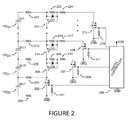
- FIG. 2shows a first balancing circuit schematic
- FIG. 3shows a balancing method flow chart.
- FIG. 4is a chart showing three series-connected cells undergoing equalization.
- FIG. 5shows a second balancing circuit schematic
- FIG. 6shows a third balancing circuit schematic.
- the term “ultracapacitor”refers to any capacitor exhibiting a very large capacitance, including but not limited to pseudocapacitors, supercapacitors, and double layer capacitors (DLC).
- the term “double layer capacitor” (DLC)refers to any device which exhibits capacitor-like characteristics and has a high capacitance.
- the term “balancing” (“equalizing”)refers to the process by which the individual cell voltages of interconnected ultracapacitors are made to be approximately equal through the means of external circuitry.
- the term “balancing circuit”refers to one or more components that are used to drain current from one cell.
- the present inventionis an apparatus/electrical circuit and methodology for balancing a series connected string of ultracapacitors.
- One representation of such a string of series connected ultracapacitors(DLC 1 ( 100 1 ), DLC 2 ( 100 2 ), DLC 3 ( 100 3 )) is shown in FIG. 1A .
- each capacitor in the series connected string(DLC 1n ( 100 4 ), DLC 12 ( 100 5 ), DLC 11 ( 100 6 )) can have a multitude of capacitors (DLC 2n ( 100 9 ), DLC 22 ( 100 8 ), DLC 21 ( 100 7 ), DLC nn ( 100 12 ), DLC n2 ( 100 11 ), DLC n1 ( 100 10 )) in parallel with it, as shown in FIG. 1B .
- the preferred embodiment of the present inventionmaximizes the amount of energy that can be stored in a series connected string of ultracapacitors without charging beyond the cell voltage rating.
- ultracapacitor cells in a series connected stringare charged to the largest voltage cell and all the cells are not equal in voltage, then the entire string stores less energy than possible.
- the maximum amount of energyis stored in series connected cells when all cell voltages are equal and charged to their maximum voltage. This balancing circuit and method causes all cells to be equal in voltage so that the maximum energy can be stored.
- the balancing circuit shown in FIG. 2allows current to be drained from each individual cell. This operation is controlled by ground referenced digital signals from a digital controller 250 with a separate control line providing an on/off signal for the balancing circuit of each cell.
- a signal of 0 indicated by zero volts reference to ground (GND)turns off a drain current from a corresponding cell and a signal of 1 indicated by a non-zero voltage higher than the gate threshold voltage of transistors 202 , 207 , 214 , and 219 in FIG. 2 activates a circuit which causes a current to flow from a corresponding cell.
- FIG. 2shows an embodiment of a balancing circuit, which balances multiple cells.
- the circuitis not limited to any particular number of cells.
- the basic balancing circuit for one cellis formed by the circuit composed of resistors: 203 , 204 , 208 , 209 , 210 ; transistors: 205 and 207 ; and zener diode 206 .
- the circuitworks in the following way. When the signal at the gate of transistor 207 is equal to 0 volts, the gate source voltage (Vgs) is equal to 0 volts and therefore transistor 207 is not conducting current.
- Vgsgate source voltage
- I DLCC ⁇ d V d t
- the previously described operationallows the cells to be equalized by draining current from the cells with higher voltages.
- the circuit composed of elements 200 , 201 , 202 , and 203is different than the above-described circuit. It balances the very first cell (the cell closest to ground) in a series connected string, which is DLC 1 ( 100 20 ) in FIG. 2 . While the circuit could be the same as the previously described circuit, it is unnecessary and therefore in this embodiment it is simpler. It uses only the N-channel mosfet because the negative terminal is connected to ground, and therefore the voltage of the cell DLC 1 ( 100 20 ) is always in reference to ground. In order to cause a current to flow from DLC 1 ( 100 20 ) through resistor 203 and 200 and mosfet 202 , a signal voltage is applied to the gate of mosfet 202 . As with the previously described circuit, this causes the voltage of DLC to decrease as current is drained from it.
- Resistors 200 , 203 , 208 , 215 , and 222have a small resistance value, which is chosen to arrive at the desired balancing current.
- the desired balancing currentis dependant on the particular applications and the size of cells used. In most applications, this resistance will be a value of less than 100 ⁇ .
- the resistors 201 , 204 , 211 , and 218are used to ensure the N-channel mosfets 202 , 207 , 214 , and 219 are not conducting by pulling the gate-to-source voltages (Vgs) to zero when the circuit is not in operation.
- the zener diodes 206 , 213 , and 221 in FIG. 2exist to ensure that the source to gate voltage Vgs of the P-channel mosfets 205 , 212 , and 220 does not exceed the maximum voltage of the device. If a sufficient number of ultracapacitors are connected in a series string the maximum allowable voltage of Vsg could be exceeded.
- the maximum voltage from source to gate of a mosfetis typically 20V and is often closer to 10V for mosfets that are designed for low voltage operation.
- the zener diodes 206 , 213 , and 221are sometimes designed as an integrated part of an OEM mosfet device. The diodes can either be separate external components or an integrated part of the mosfet.
- FIG. 2is shows a balancing circuit for four ultracapacitors connected in series.
- the circuitcomposed of resistors: 215 , 218 , 222 , 223 , and 224 ; transistor 220 and 219 ; and zener diode 211 , represent a circuit which repeats with additional connected ultracapacitors.
- the circuitis not limited to any particular number of cells.
- the transistors in this embodimentare mosfets, however other forms of transistors may be used (e.g., bi-polar junction transistors (BJTs), phototransistors, insulated gate bipolar transistors (IGBT), junction field effect transistors (JEFT)).
- BJTsbi-polar junction transistors
- IGBTinsulated gate bipolar transistors
- JEFTjunction field effect transistors
- Additional resistors 216 , 217 and additional series connected strings DLC( 100 24 ), DLC 3 ( 100 23 )are shown as well.
- the circuit of FIG. 2allows for ground referenced digital (on/off) signals like what might come from a digital controller to drain current from individual cells in large series connected strings of ultracapacitors.
- the previously described circuit(shown in FIG. 2 ) allows the voltages of the cells to be drained down so that they all have approximately the same voltage.
- the method illustrated in FIG. 3describes by what process the balancing actually occurs in the preferred embodiment.
- a separate analog circuit(not shown in FIG. 2 ) be connected to the terminals of each ultracapacitor in a series string.
- the circuittakes a differential voltage signal and converts it to a ground-referenced signal that can be read by a digital controller.
- the digital controlleruses these voltages in the following method, which is shown in flow diagram form in FIG. 3 .
- the methoddrains a relatively small amount of current from every cell except for the lowest voltage cell. In this way, the voltages of the cells become very close to being all equal to each other or in other words balanced or equalized.
- step 500the digital controller first specifies the variable “V_BAL_HYST,” which stands for “voltage balance hysteresis.” This value will indicate how closely the cells become balanced to each other. The use of this variable is advantageous because it is typically necessary to only balance cell voltages to some specific voltage. Attempting to balance cells to very small voltages is not useful and wastes energy.
- V_BAL_HYSTthe main process loop is entered.
- step 510all of the balancing circuits are turned off and therefore none of the balancing circuits are draining current from any of the cells. This is done because in some embodiments the draining current from the cells could affect the accurate measurement of the cell voltages.
- step 520the voltage of each cell is measured by means of said analog measurement circuit.
- step 530the smallest measured cell voltage in the series connected string is determined.
- step 540said smallest voltage is stored in a variable called “V min .”
- step 550the voltage of the first cell in the series string minus V min is compared to “V_BAL_HYST.” If the result of the subtraction is greater than “V_BAL_HYST,” in step 555 the balancing circuit for that cell is turned on where current is drained from the cell. If the result of the subtraction is not greater than “V_BAL_HYST,” the circuit for the corresponding cell is not turned on and therefore remains in the off state where no current is drained from the cell.
- step 580an artificial time delay is employed. This is used to make sure the cells have an adequate time to balance before the loop repeats and all balancing circuits are shut off.
- this loopis cyclical and because it requires a finite amount of time to execute the described process, the result is a square wave type of balancing signal of which the off and on time for each engaged balancing circuit will depend on the amount of time delay and the amount of processing time for each operation.
- FIG. 4is a graph illustrating the cell voltage (V) of three series-connecting cells undergoing equalization over a period of time (minutes) via one embodiment of the present invention.
- FIG. 5shows a balancing circuit schematic embodiment using bipolar junction transistors (BJT) for four ultracapacitors connected in series.
- BJTbipolar junction transistors
- the circuitcomposed of elements 200 , 301 , 302 , 303 and 203 balances the very first cell (the cell closest to ground) in a series connected string, which is DLC 1 ( 100 20 ).
- This circuituses only one BJT because the negative terminal is connected to ground, and therefore the voltage of the cell DLC 1 ( 100 20 ) is always in reference to ground.
- a signal voltageis applied to the base of BJT 301 . This causes the voltage of DLC to decrease as current is drained from it.
- Resistors 200 , 203 , 208 , 215 , and 222have a small resistance value, which is chosen to arrive at the desired balancing current.
- the desired balancing currentis dependant on the particular applications and the size of cells used. In most applications, this resistance will be a value of less than 100 ⁇ .
- the resistors 302 , 309 , 315 , and 321are used to ensure the BJTs 301 , 308 , 314 , and 320 (and likewise resistors 306 , 312 , and 318 for BJTs 304 , 311 , and 317 respectively) are not conducting by pulling the base to emitter voltages (Vbe) to zero when the circuit is not in operation.
- the resistors 303 , 310 , 316 and 322 in FIG. 2exist to limit the base current Ib of the BJTs 301 , 308 , 314 and 320 (and likewise resistors 307 , 313 , and 319 for BJTs 304 , 311 317 respectively).
- FIG. 6shows a balancing circuit schematic embodiment using phototransistors (e.g., phototransistor optocoupler) for four ultracapacitors connected in series.
- the circuitcomposed of elements 200 , 203 , 401 , and 402 balances the very first cell (the cell closest to ground) in a series connected string, which is DLC 1 ( 100 20 ).
- DLC 1the cell closest to ground
- a signal voltageis applied to the input (anode) of phototransistor 401 . This causes the voltage of DLC to decrease as current is drained from it.
- Resistors 200 , 203 , 208 , 215 , and 222have a small resistance value, which is chosen to arrive at the desired balancing current.
- Resistors 402 , 404 , 406 , 408exist to limit current into the input of the phototransistor optocoupler, similar to how resistors are used in the BJT circuit ( FIG. 5 ) to limit current.
- the desired balancing currentis dependent on the particular applications and the size of cells used. In most applications, this resistance will be a value of less than 100 ⁇ .
- the circuit composed of resistors: 215 , 222 , 408 , and phototransistor 407represent a circuit which repeats with additional connected ultracapacitors. The circuit is not limited to any particular number of cells.
- DLC( 100 24 ), DLC 3 ( 100 23 )are shown as well.
- the preferred phototransistorbeing general purpose 6-pin phototransistor optocouplers manufactured by Fairchild Semiconductor (e.g, model numbers 4N25, 4N26, 4N27, 4N28, 4N35, 4N36, 4N37, H11A1, H11A2, H11A3, H11A4, H11A5),
- the “Distinct-Voltage-Drain Circuit” of the prior artonly drains current when the cell is fully charged.
- the cellsonly become balanced when the string is at its maximum voltage for a time sufficient to drain the higher voltage cells.
- the present invention's circuit and methodcan balance cells at voltages less than the maximum voltage and therefore intelligently determines when it is and is not appropriate to balance.
- a digital controllermeasures each individual voltage and intelligently balances every cell voltage in a string.
- mosfet transistorsWhile the use of mosfet transistors is disclosed, there exist other types of transistors that would work in the place of N-channel and P-channel mosfets. Possible substitution types include but are not limited to phototransistors, BJTs (bi-polar junction transistors) and IGBT (insulated gate bipolar transistors).
- An ultracapacitor charging method for charging a series connected string of ultracapacitor cells having a plurality of balancing circuitscomprising the steps of: (a) specifying a voltage balance hysteresis as variable V_BAL_HYST; (b) charging said string of ultracapacitor cells; (c) turning all balancing circuits off; (d) measuring the voltage of each ultracapacitor cell to determine the smallest measured cell voltage; (e) storing said smallest measured cell voltage as variable V min ; and (f) for each ultracapacitor cell in the series connected string iteratively performing the following steps: (i) measuring the voltage of the ultracapacitor cell to set Vcell; (ii) computing the difference of Vcell and V min ; (iii) comparing difference of Vcell and V min to V_BAL_HYST, wherein if the difference of Vcell and V min >V_BAL_HYST, then turning on the balancing circuit for the cell
- the step of measuring the voltage of each ultracapacitor cell to determine the smallest measured cell voltageis performed via an analog measurement circuit.
- the step of charging said string of ultracapacitor cellsis performed by a device which transfers charge in a controlled fashion (e.g., charger).
- the step of specifying a voltage balance hysteresis as variable V_BAL_HYSTis performed by a digital controller.
- steps (c), (d), (e) and (f)are repeated.
- An apparatus for charging a series connected string of ultracapacitor cellscomprising: a charger for charging said string of ultracapacitor cells; a plurality of balancing circuits for draining current from the cell; and a digital controller, said digital controller specifying a voltage balance hysteresis as variable V_BAL_HYST, said digital controller turning all balancing circuits off, determining which cell has the smallest cell voltage (V min ), wherein as the ultracapacitor cells charge said digital controller monitors the voltage of each of the ultracapacitor cells, turning the corresponding balancing circuit on for any ultracapacitor cells where the difference between the voltage of the ultracapacitor cell and V min >V_BAL_HYST.
- an analog measurement circuitis utilized to measure the voltage of each ultracapacitor cell so that said digital controller can determine the smallest measured cell voltage.
- an artificial time delay for providing said ultracapacitor cells with an adequate time to balancewherein after said time delay said digital controller turning all balancing circuits off, determining which cell has the smallest cell voltage (V min ), wherein as the ultracapacitor cells charge said digital controller monitors the voltage of each of the ultracapacitor cells, turning the corresponding balancing circuit on for any ultracapacitor cells where the difference between the voltage of the ultracapacitor cell and V min >V_BAL_HYST.
Landscapes
- Engineering & Computer Science (AREA)
- Power Engineering (AREA)
- Microelectronics & Electronic Packaging (AREA)
- Charge And Discharge Circuits For Batteries Or The Like (AREA)
Abstract
Description
Resistance 209>>Resistance 210
the voltage drop is much greater overresistor 209. This operation provides adequate voltage from source to gate of P-channel mosfet 206 to cause it to conduct current. In this embodiment,resistor 209 is one magnitude greater thanresistor 210. Asmosfet 206 is conducting, current flows from DLC2 (10021) throughresistors mosfet 205. This operation causes the voltage of DLC2 to decrease. This can be seen from the following equation which is the equation describing an ideal capacitor.
Claims (20)
Priority Applications (1)
| Application Number | Priority Date | Filing Date | Title |
|---|---|---|---|
| US12/540,281US8269469B2 (en) | 2008-08-12 | 2009-08-12 | Equalizing method and circuit for ultracapacitors |
Applications Claiming Priority (2)
| Application Number | Priority Date | Filing Date | Title |
|---|---|---|---|
| US8821308P | 2008-08-12 | 2008-08-12 | |
| US12/540,281US8269469B2 (en) | 2008-08-12 | 2009-08-12 | Equalizing method and circuit for ultracapacitors |
Publications (2)
| Publication Number | Publication Date |
|---|---|
| US20100039072A1 US20100039072A1 (en) | 2010-02-18 |
| US8269469B2true US8269469B2 (en) | 2012-09-18 |
Family
ID=41680867
Family Applications (1)
| Application Number | Title | Priority Date | Filing Date |
|---|---|---|---|
| US12/540,281Expired - Fee RelatedUS8269469B2 (en) | 2008-08-12 | 2009-08-12 | Equalizing method and circuit for ultracapacitors |
Country Status (1)
| Country | Link |
|---|---|
| US (1) | US8269469B2 (en) |
Cited By (6)
| Publication number | Priority date | Publication date | Assignee | Title |
|---|---|---|---|---|
| US20120062187A1 (en)* | 2010-09-13 | 2012-03-15 | Samsung Electronics Co., Ltd | Auxiliary power device, memory system having the same, and cell balancing method thereof |
| US9072572B2 (en) | 2009-04-02 | 2015-07-07 | Kerr Corporation | Dental light device |
| US9572643B2 (en) | 1998-01-20 | 2017-02-21 | Kerr Corporation | Apparatus and method for curing materials with radiation |
| US9730778B2 (en) | 2009-04-02 | 2017-08-15 | Kerr Corporation | Curing light device |
| US20210408807A1 (en)* | 2020-06-30 | 2021-12-30 | Avx Corporation | System and Method for Balancing Ultracapacitors |
| US11239670B2 (en)* | 2018-09-16 | 2022-02-01 | Richard Landry Gray | Cell balancing battery module and electrical apparatus |
Families Citing this family (14)
| Publication number | Priority date | Publication date | Assignee | Title |
|---|---|---|---|---|
| JP5567956B2 (en) | 2010-09-16 | 2014-08-06 | 矢崎総業株式会社 | Cell voltage equalization device for multiple assembled batteries |
| US20120119709A1 (en)* | 2010-11-17 | 2012-05-17 | Tenergy Corporation | Battery pack balancing circuit |
| US9331500B2 (en) | 2012-04-19 | 2016-05-03 | Caterpillar Inc. | Method for balancing ultracapacitor cells |
| EP3065260A1 (en)* | 2015-03-04 | 2016-09-07 | Illinois Tool Works Inc. | Ground power unit with lower noise and pollution emission |
| CN106786944B (en)* | 2016-12-31 | 2020-12-18 | 华为技术有限公司 | A sampling circuit, equalization circuit and system of single cells in series battery pack |
| US10374440B2 (en)* | 2017-06-22 | 2019-08-06 | Rockwell Collins, Inc. | System and method for supercapacitor charging and balancing |
| EP3616223B1 (en) | 2017-06-30 | 2022-06-01 | KYOCERA AVX Components Corporation | Balancing circuit for an ultracapacitor module |
| US10879720B2 (en)* | 2017-07-21 | 2020-12-29 | Avx Corporation | Balancing circuit for an electrical energy storage device |
| CN111786426B (en)* | 2020-05-20 | 2022-05-03 | 宁波中车新能源科技有限公司 | Passive CMS equalization circuit and method based on super capacitor |
| WO2021247315A1 (en)* | 2020-06-02 | 2021-12-09 | Avx Corporation | Ultracapacitor assembly |
| US12136837B1 (en)* | 2020-12-08 | 2024-11-05 | Bobbie Wilson | Charge balancing of parallel strings with zener diode and light emitting diode between cell terminal of the battery strings |
| CN114421559A (en)* | 2021-12-30 | 2022-04-29 | 杭州元色科技有限公司 | Ignition starting device |
| CN114624605B (en)* | 2022-02-25 | 2025-04-29 | 广州市仟顺电子设备有限公司 | Battery monitoring equipment calibration device, method and system |
| CN115436824B (en)* | 2022-11-08 | 2023-03-24 | 苏州浪潮智能科技有限公司 | Super capacitor test method and device, electronic equipment and storage medium |
Citations (28)
| Publication number | Priority date | Publication date | Assignee | Title |
|---|---|---|---|---|
| US5222012A (en)* | 1991-01-17 | 1993-06-22 | International Business Machines Corporation | Power management circuit for a magnetic repulsion punch |
| EP0564149A2 (en) | 1992-04-03 | 1993-10-06 | JEOL Ltd. | Storage capacitor power supply |
| US5952815A (en) | 1997-07-25 | 1999-09-14 | Minnesota Mining & Manufacturing Co. | Equalizer system and method for series connected energy storing devices |
| US5969505A (en) | 1996-12-05 | 1999-10-19 | Jeol Ltd. | Charging system for charging capacitors of a capacitor bank |
| US20020177018A1 (en)* | 2001-05-23 | 2002-11-28 | Fuglevand William A. | Fuel cell power system, method of distributing power, and method of operating a fuel cell power system |
| US20030214267A1 (en) | 2002-05-20 | 2003-11-20 | Long Laurence P. | Ultracapacitor balancing circuit |
| US6714391B2 (en) | 2001-10-04 | 2004-03-30 | Ise Research Corporation | Ultracapacitor energy storage cell pack and methods of assembling and cooling the same |
| US6777917B2 (en) | 2001-06-18 | 2004-08-17 | Alcatel | Supercapacitor balancing method and system |
| US6806686B1 (en) | 2003-04-25 | 2004-10-19 | Maxwell Technologies, Inc. | Charge balancing circuit |
| US6841971B1 (en) | 2002-05-29 | 2005-01-11 | Alpha Technologies, Inc. | Charge balancing systems and methods |
| US6844704B2 (en) | 2001-10-04 | 2005-01-18 | Ise Corp. | Voltage threshold device and energy storage cell failure detection system for power supply |
| US7042197B2 (en) | 2001-12-21 | 2006-05-09 | Energy Storage Systems Pto Ltd | Control circuit |
| US7085112B2 (en) | 2001-10-04 | 2006-08-01 | Ise Corporation | High-power ultracapacitor energy storage pack and method of use |
| US20060176028A1 (en)* | 2004-11-15 | 2006-08-10 | Schulte Juergen J | System and method for precharging and discharging a high power ultracapacitor pack |
| US20060194102A1 (en) | 2003-02-13 | 2006-08-31 | Sarkis Keshishian | Resistive balance for an energy storage device |
| US20070002518A1 (en) | 2001-10-04 | 2007-01-04 | Ise Corporation | High-Power Ultracapacitor Energy Storage Pack and Method of Use |
| US7193390B2 (en)* | 2002-05-17 | 2007-03-20 | Sony Corporation | Apparatus for connecting secondary battery cells in series and method for controlling secondary battery cells connected in series |
| US7206705B2 (en) | 2002-08-07 | 2007-04-17 | Siemens Aktiengesellschaft | Method and apparatus for balancing capacitors in a capacitor bank |
| US7218489B2 (en) | 2001-10-04 | 2007-05-15 | Ise Corporation | High-power ultracapacitor energy storage pack and method of use |
| US20080106239A1 (en) | 2006-11-03 | 2008-05-08 | Cegnar Erik J | Ultra-fast ultracapacitor pack/device charger |
| US20080157721A1 (en)* | 2006-12-28 | 2008-07-03 | Nissan Motor Co., Ltd. | Battery pack capacity adjusting device and method |
| US20080169791A1 (en)* | 2007-01-17 | 2008-07-17 | Omron Corporation | Capacitor charging control circuit |
| US20080211459A1 (en)* | 2007-03-02 | 2008-09-04 | Won-Suk Choi | Battery management system and driving method thereof |
| US7463009B2 (en)* | 2006-07-17 | 2008-12-09 | Compal Electronics, Inc. | Hybrid battery module with a voltage balancing unit and its charging and discharging method |
| US20080303484A1 (en)* | 2004-12-24 | 2008-12-11 | Lg Chem, Ltd. | System For Controlling Voltage Balancing In a Plurality of Lithium-Ion Cell Battery Packs and Method Thereof |
| US7573151B2 (en)* | 2007-10-11 | 2009-08-11 | Lear Corporation | Dual energy-storage for a vehicle system |
| US20100019732A1 (en)* | 2006-11-06 | 2010-01-28 | Nec Corporation | Electric cells for battery pack, battery control system, and battery control method |
| US7750607B2 (en)* | 2005-08-31 | 2010-07-06 | Panasonic Corporation | Auxiliary electric power supply for vehicle and charger/discharger for vehicle |
- 2009
- 2009-08-12USUS12/540,281patent/US8269469B2/ennot_activeExpired - Fee Related
Patent Citations (29)
| Publication number | Priority date | Publication date | Assignee | Title |
|---|---|---|---|---|
| US5222012A (en)* | 1991-01-17 | 1993-06-22 | International Business Machines Corporation | Power management circuit for a magnetic repulsion punch |
| EP0564149A2 (en) | 1992-04-03 | 1993-10-06 | JEOL Ltd. | Storage capacitor power supply |
| US5969505A (en) | 1996-12-05 | 1999-10-19 | Jeol Ltd. | Charging system for charging capacitors of a capacitor bank |
| US5952815A (en) | 1997-07-25 | 1999-09-14 | Minnesota Mining & Manufacturing Co. | Equalizer system and method for series connected energy storing devices |
| US20020177018A1 (en)* | 2001-05-23 | 2002-11-28 | Fuglevand William A. | Fuel cell power system, method of distributing power, and method of operating a fuel cell power system |
| US6777917B2 (en) | 2001-06-18 | 2004-08-17 | Alcatel | Supercapacitor balancing method and system |
| US7218489B2 (en) | 2001-10-04 | 2007-05-15 | Ise Corporation | High-power ultracapacitor energy storage pack and method of use |
| US6714391B2 (en) | 2001-10-04 | 2004-03-30 | Ise Research Corporation | Ultracapacitor energy storage cell pack and methods of assembling and cooling the same |
| US6844704B2 (en) | 2001-10-04 | 2005-01-18 | Ise Corp. | Voltage threshold device and energy storage cell failure detection system for power supply |
| US7085112B2 (en) | 2001-10-04 | 2006-08-01 | Ise Corporation | High-power ultracapacitor energy storage pack and method of use |
| US20060262467A1 (en) | 2001-10-04 | 2006-11-23 | Ise Corporation | High-Power Ultracapacitor Energy Storage Pack and Method of Use |
| US20070002518A1 (en) | 2001-10-04 | 2007-01-04 | Ise Corporation | High-Power Ultracapacitor Energy Storage Pack and Method of Use |
| US7042197B2 (en) | 2001-12-21 | 2006-05-09 | Energy Storage Systems Pto Ltd | Control circuit |
| US7193390B2 (en)* | 2002-05-17 | 2007-03-20 | Sony Corporation | Apparatus for connecting secondary battery cells in series and method for controlling secondary battery cells connected in series |
| US20030214267A1 (en) | 2002-05-20 | 2003-11-20 | Long Laurence P. | Ultracapacitor balancing circuit |
| US6841971B1 (en) | 2002-05-29 | 2005-01-11 | Alpha Technologies, Inc. | Charge balancing systems and methods |
| US7206705B2 (en) | 2002-08-07 | 2007-04-17 | Siemens Aktiengesellschaft | Method and apparatus for balancing capacitors in a capacitor bank |
| US20060194102A1 (en) | 2003-02-13 | 2006-08-31 | Sarkis Keshishian | Resistive balance for an energy storage device |
| US6806686B1 (en) | 2003-04-25 | 2004-10-19 | Maxwell Technologies, Inc. | Charge balancing circuit |
| US20060176028A1 (en)* | 2004-11-15 | 2006-08-10 | Schulte Juergen J | System and method for precharging and discharging a high power ultracapacitor pack |
| US20080303484A1 (en)* | 2004-12-24 | 2008-12-11 | Lg Chem, Ltd. | System For Controlling Voltage Balancing In a Plurality of Lithium-Ion Cell Battery Packs and Method Thereof |
| US7750607B2 (en)* | 2005-08-31 | 2010-07-06 | Panasonic Corporation | Auxiliary electric power supply for vehicle and charger/discharger for vehicle |
| US7463009B2 (en)* | 2006-07-17 | 2008-12-09 | Compal Electronics, Inc. | Hybrid battery module with a voltage balancing unit and its charging and discharging method |
| US20080106239A1 (en) | 2006-11-03 | 2008-05-08 | Cegnar Erik J | Ultra-fast ultracapacitor pack/device charger |
| US20100019732A1 (en)* | 2006-11-06 | 2010-01-28 | Nec Corporation | Electric cells for battery pack, battery control system, and battery control method |
| US20080157721A1 (en)* | 2006-12-28 | 2008-07-03 | Nissan Motor Co., Ltd. | Battery pack capacity adjusting device and method |
| US20080169791A1 (en)* | 2007-01-17 | 2008-07-17 | Omron Corporation | Capacitor charging control circuit |
| US20080211459A1 (en)* | 2007-03-02 | 2008-09-04 | Won-Suk Choi | Battery management system and driving method thereof |
| US7573151B2 (en)* | 2007-10-11 | 2009-08-11 | Lear Corporation | Dual energy-storage for a vehicle system |
Cited By (10)
| Publication number | Priority date | Publication date | Assignee | Title |
|---|---|---|---|---|
| US9572643B2 (en) | 1998-01-20 | 2017-02-21 | Kerr Corporation | Apparatus and method for curing materials with radiation |
| US9622839B2 (en) | 1998-01-20 | 2017-04-18 | Kerr Corporation | Apparatus and method for curing materials with radiation |
| US9072572B2 (en) | 2009-04-02 | 2015-07-07 | Kerr Corporation | Dental light device |
| US9693846B2 (en) | 2009-04-02 | 2017-07-04 | Kerr Corporation | Dental light device |
| US9730778B2 (en) | 2009-04-02 | 2017-08-15 | Kerr Corporation | Curing light device |
| US9987110B2 (en) | 2009-04-02 | 2018-06-05 | Kerr Corporation | Dental light device |
| US20120062187A1 (en)* | 2010-09-13 | 2012-03-15 | Samsung Electronics Co., Ltd | Auxiliary power device, memory system having the same, and cell balancing method thereof |
| US9252603B2 (en)* | 2010-09-13 | 2016-02-02 | Samsung Electronics Co., Ltd. | Auxiliary power device, memory system having the same, and cell balancing method thereof |
| US11239670B2 (en)* | 2018-09-16 | 2022-02-01 | Richard Landry Gray | Cell balancing battery module and electrical apparatus |
| US20210408807A1 (en)* | 2020-06-30 | 2021-12-30 | Avx Corporation | System and Method for Balancing Ultracapacitors |
Also Published As
| Publication number | Publication date |
|---|---|
| US20100039072A1 (en) | 2010-02-18 |
Similar Documents
| Publication | Publication Date | Title |
|---|---|---|
| US8269469B2 (en) | Equalizing method and circuit for ultracapacitors | |
| US10566804B2 (en) | Method of forming a balancing circuit for a plurality of battery cells | |
| KR101754111B1 (en) | Adaptive overvoltage protection circuit and method, and power system including the same | |
| US20130314068A1 (en) | Temperature adaptive bandgap reference circuit | |
| US20100109607A1 (en) | Battery Array Voltage Equalization Device | |
| US10637270B2 (en) | Battery charging circuit and charging method thereof | |
| JP2021501325A (en) | Failure determination method for battery management system, battery pack including it, and current measurement circuit | |
| US8198869B2 (en) | System and method for charging capacitors using automatic cell balancing | |
| ATE471592T1 (en) | INTEGRATED CIRCUIT FOR PROVIDING A CURRENT-CONTROLLED CHARGE PUMP WITH CURRENT PROPORTIONAL TO THE CAPACITOR | |
| CN101159410A (en) | Control circuit method and apparatus responsive to impedance coupled to control circuit terminals | |
| CN101976960A (en) | Switching power supply peak current control device and method | |
| US9977088B2 (en) | Battery fuel gauge current sensing circuit and method thereof | |
| US20130026974A1 (en) | Charging circuit and charging control method | |
| EP2639924A2 (en) | Charge control circuit | |
| US20120262148A1 (en) | Voltage measurement apparatus | |
| CN102998622A (en) | Remote controller and battery voltage detection method and device thereof | |
| CN106199299A (en) | The system and method for the short-circuit detecting in load bearing chain | |
| US20150070949A1 (en) | Device for transfering power from a first circuit to a second circuit | |
| WO2023250234A2 (en) | Integrated circuit package with internal circuitry to detect external component parameters and parasitics | |
| US7696726B2 (en) | Battery charger and associated method | |
| CN102955071B (en) | balance resistance testing device | |
| US10122185B2 (en) | Battery management system | |
| TWI463762B (en) | Method of balanced charging for combinational batteries | |
| CN102270885A (en) | Method and apparatus for balancing the voltage of a series connection of electrical energy storage units | |
| CN104518646A (en) | Controller for adjusting output voltage of power converter and related method thereof |
Legal Events
| Date | Code | Title | Description |
|---|---|---|---|
| AS | Assignment | Owner name:IVUS INDUSTRIES, INC.,IDAHO Free format text:ASSIGNMENT OF ASSIGNORS INTEREST;ASSIGNORS:CEGNAR, ERIK;JESSUP, FRED;MAUGHAN, MICHAEL;AND OTHERS;SIGNING DATES FROM 20090930 TO 20091005;REEL/FRAME:023343/0430 Owner name:IVUS INDUSTRIES, INC., IDAHO Free format text:ASSIGNMENT OF ASSIGNORS INTEREST;ASSIGNORS:CEGNAR, ERIK;JESSUP, FRED;MAUGHAN, MICHAEL;AND OTHERS;SIGNING DATES FROM 20090930 TO 20091005;REEL/FRAME:023343/0430 | |
| AS | Assignment | Owner name:IVUS INDUSTRIES, LLC, IDAHO Free format text:CORRECTIVE ASSIGNMENT TO CORRECT THE ASSIGNEE NAME (LLC INSTEAD OF INC) PREVIOUSLY RECORDED ON REEL 023343 FRAME 0430. ASSIGNOR(S) HEREBY CONFIRMS THE ASSIGNMENT OF RIGHTS, TITLE AND INTEREST IN INVENTION;ASSIGNORS:CEGNAR, ERIK;JESSUP, FRED;MAUGHAN, MICHAEL;AND OTHERS;SIGNING DATES FROM 20090930 TO 20091005;REEL/FRAME:025205/0805 | |
| STCF | Information on status: patent grant | Free format text:PATENTED CASE | |
| REMI | Maintenance fee reminder mailed | ||
| FPAY | Fee payment | Year of fee payment:4 | |
| SULP | Surcharge for late payment | ||
| AS | Assignment | Owner name:DAN J. AND DENISE L. COSTA 1997 FAMILY TRUST, CALI Free format text:ASSIGNMENT OF ASSIGNORS INTEREST;ASSIGNOR:IVUS INDUSTRIES, LLC;REEL/FRAME:041889/0378 Effective date:20160713 | |
| FEPP | Fee payment procedure | Free format text:MAINTENANCE FEE REMINDER MAILED (ORIGINAL EVENT CODE: REM.); ENTITY STATUS OF PATENT OWNER: SMALL ENTITY | |
| LAPS | Lapse for failure to pay maintenance fees | Free format text:PATENT EXPIRED FOR FAILURE TO PAY MAINTENANCE FEES (ORIGINAL EVENT CODE: EXP.); ENTITY STATUS OF PATENT OWNER: SMALL ENTITY | |
| STCH | Information on status: patent discontinuation | Free format text:PATENT EXPIRED DUE TO NONPAYMENT OF MAINTENANCE FEES UNDER 37 CFR 1.362 | |
| FP | Lapsed due to failure to pay maintenance fee | Effective date:20200918 |