US8269233B2 - Vertical ACLED structure - Google Patents
Vertical ACLED structureDownload PDFInfo
- Publication number
- US8269233B2 US8269233B2US12/588,745US58874509AUS8269233B2US 8269233 B2US8269233 B2US 8269233B2US 58874509 AUS58874509 AUS 58874509AUS 8269233 B2US8269233 B2US 8269233B2
- Authority
- US
- United States
- Prior art keywords
- acled
- semiconductor layer
- type electrode
- opto
- type semiconductor
- Prior art date
- Legal status (The legal status is an assumption and is not a legal conclusion. Google has not performed a legal analysis and makes no representation as to the accuracy of the status listed.)
- Expired - Fee Related, expires
Links
Images


Classifications
- H—ELECTRICITY
- H01—ELECTRIC ELEMENTS
- H01L—SEMICONDUCTOR DEVICES NOT COVERED BY CLASS H10
- H01L25/00—Assemblies consisting of a plurality of semiconductor or other solid state devices
- H01L25/03—Assemblies consisting of a plurality of semiconductor or other solid state devices all the devices being of a type provided for in a single subclass of subclasses H10B, H10D, H10F, H10H, H10K or H10N, e.g. assemblies of rectifier diodes
- H01L25/04—Assemblies consisting of a plurality of semiconductor or other solid state devices all the devices being of a type provided for in a single subclass of subclasses H10B, H10D, H10F, H10H, H10K or H10N, e.g. assemblies of rectifier diodes the devices not having separate containers
- H01L25/075—Assemblies consisting of a plurality of semiconductor or other solid state devices all the devices being of a type provided for in a single subclass of subclasses H10B, H10D, H10F, H10H, H10K or H10N, e.g. assemblies of rectifier diodes the devices not having separate containers the devices being of a type provided for in group H10H20/00
- H01L25/0756—Stacked arrangements of devices
- H—ELECTRICITY
- H01—ELECTRIC ELEMENTS
- H01L—SEMICONDUCTOR DEVICES NOT COVERED BY CLASS H10
- H01L2924/00—Indexing scheme for arrangements or methods for connecting or disconnecting semiconductor or solid-state bodies as covered by H01L24/00
- H01L2924/0001—Technical content checked by a classifier
- H01L2924/0002—Not covered by any one of groups H01L24/00, H01L24/00 and H01L2224/00
Definitions
- This applicationrelated to a structure of ACLED, especially related to a vertical stack ACLED structure.
- the light-emitting diodes (LEDs) of the solid-state lighting elementshave the characteristics of low power consumption, low heat generation, long operational life, shockproof, small volume, quick response and good opto-electrical property like light emission with a stable wavelength, so the LEDs have been widely used in household appliances, indicator light of instruments, and opto-electrical products, etc. As the opto-electrical technology develops, the solid-state lighting elements have great progress in the light efficiency, operation life and the brightness, and LEDs are expected to become the main stream of the lighting devices in the near future.
- the conventional LEDis driven by direct current (DC).
- DCdirect current
- An AC-DC inverteris required to invert DC to AC. Since the inverter has large volume and heavy weight, the cost is added and the power is loss during inverting. Therefore, it is difficult for LED to compete with the existing light source mainly because of the price concern.
- the ACLEDcan solve the problems mentioned above. It can decrease the volume and weight of LED, extend to more applications, decrease the cost in inverter element, and decrease the 15 ⁇ 30% power loss of conventional DC-AC in inverting so the light efficiency of the whole LED is increased.
- the ACLEDsnormally keep the growth substrate such as sapphire to form an anti-parallel connection structure in horizontal orientation, so the size is as twice as that of the conventional single chip. Accordingly, the space and cost is wasted.
- This applicationrelates to an opto-electrical device comprising a first ACLED having a first n-type semiconductor layer, a first light emitting layer, a first p-type semiconductor layer, a first p-type electrode and a first n-type electrode; a second ACLED having a second n-type semiconductor layer, a second light emitting layer, a second p-type semiconductor layer, a second p-type electrode and a second n-type electrode, wherein each of the first ACLED and the second ACLED are vertical stack structure and is connected in anti-parallel manner.
- FIG. 1illustrates a cross-sectional view of the vertical stack ACLED structure in accordance with one embodiment of the present application.
- FIG. 2illustrates a cross-sectional view of the vertical stack ACLED structure in accordance with one embodiment of the present application.
- FIG. 3illustrates a cross-sectional view of the vertical stack ACLED structure in accordance with one embodiment of the present application.
- FIG. 4illustrates a cross-sectional view of the vertical stack ACLED structure in accordance with one embodiment of the present application.
- This applicationrelates to a structure of ACLED, especially relates to a vertical stack ACLED structure.
- This applicationconnects respective p-type and n-type electrode of at least two ACLEDs which emitting light with the same or different wavelength in anti-parallel manner to form a vertical stack ACLED structure by wafer bonding, chip form bonding or flip-chip bonding in wafer or chip level.
- the vertical stack ACLED structure of this applicationcan decrease the area occupied by the chip.
- the ACLED structure in the same spacecan emit light under different voltage phase when the ACLEDs are connected in anti-parallel manner by wafer bonding, chip form bonding or flip-chip bonding.
- This applicationcan be used for white light emitting device by combining phosphors and ACLEDs having different wavelength. Besides, the phosphor consumed in the device of the present application is less than that used in the conventional LEDs connected in anti-parallel manner horizontally by coating the phosphor with one unit of the area under the same light emitting area.
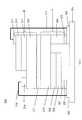
- FIG. 1illustrates a cross-sectional view of the vertical stack ACLED structure in accordance with the first embodiment of the present application.
- the structureincludes a submount 101 , a bonding layer 112 , two light emitting diodes A, B and two wires 119 , 120 .
- the bonding layer 112can be a transparent layer, and the material can be conductive material such as ITO, or insulating material such as the organic plastic material, ex: BCB, SINR, or HT250.
- the first light emitting diodes Acontains a first substrate 111 , a first n-type semiconductor layer 110 , a first light emitting layer 109 , and a first p-type semiconductor layer 108 formed on the first substrate 111 subsequently.
- the material of the first n-type semiconductor layer 110 , the first light emitting layer 109 and the first p-type semiconductor layer 108contains one or more elements selected from the group consisting of Ga, Al, In, As, P, N and Si.
- a first p-type electrode 107is formed on the first p-type semiconductor layer 108 ; a first n-type electrode 106 is formed on the first n-type semiconductor layer 110 .
- the first p-type electrode 107is connected to a p-type electrode 103 on the submount 101 by a first solder 105 ; the first n-type electrode 106 is connected to a n-type electrode 102 on the submount 101 by a second solder 104 .
- the second light emitting diodes Bcontains a second substrate 113 , a second n-type semiconductor layer 114 , a second light emitting layer 115 and a second p-type semiconductor layer 116 formed on the second substrate 113 subsequently.
- the material of the second n-type semiconductor layer 114 , the second light emitting layer 115 and the second p-type semiconductor layer 116contains one or more elements selected from the group consisting of Ga, Al, In, As, P, N and Si.
- a second p-type electrode 117is formed on the second p-type semiconductor layer 116 ; a second n-type electrode 118 is formed on the second n-type semiconductor layer 114 .
- the material of the first substrate 111 and the second substrate 113can be sapphire, SiC, ZnO or GaN.
- the first substrate 111 of the first light emitting diode A and the second substrate 113 of the second light emitting diode Bis connected by a bonding layer 112 .
- the second p-type electrode 117 of the second light emitting diode Bis connected to a n-type electrode 102 on the submount 101 by a first wire 119 ;
- the second n-type electrode 118 of the second light emitting diode Bis connected to a p-type electrode 103 on the submount 101 by a second wire 120 .
- the light emitting diode A and the light emitting diode Bare connected in anti-parallel manner to form a vertical stack structure by wafer bonding, chip form bonding or flip-chip bonding.
- FIG. 2illustrates a cross-sectional view of the vertical stack ACLED structure in accordance with a second embodiment of the present application.
- the structureincludes a submount 201 , a bonding layer 211 , two light emitting diodes A, B and two wires 217 , 218 .
- the bonding layer 211can be a transparent layer, and the material can be conductive material such as ITO, or insulating material such as the organic plastic material, ex: BCB, SINR, or HT250.
- the first light emitting diodes Acontains a first n-type semiconductor layer 210 , a first light emitting layer 209 and a first p-type semiconductor layer 208 .
- the material of the first n-type semiconductor layer 210 , the first light emitting layer 209 and the first p-type semiconductor layer 208contains one or more elements selected from the group consisting of Ga, Al, In, As, P, N and Si.
- a first p-type electrode 207is formed on the first p-type semiconductor layer 208 ; a first n-type electrode 206 is formed on the first n-type semiconductor layer 210 .
- the first p-type electrode 207is connected to a p-type electrode 203 on the submount 201 by a first solder 205 ; the first n-type electrode 206 is connected to a n-type electrode 202 on the submount 201 by a second solder 204 .
- the second light emitting diodes Bcontains a second n-type semiconductor layer 212 , a second light emitting layer 213 and a second p-type semiconductor layer 214 .
- the material of the second n-type semiconductor layer 212 , the second light emitting layer 213 and the second p-type semiconductor layer 214contains one or more elements selected from the group consisting of Ga, Al, In, As, P, N and Si.
- a second p-type electrode 215is formed on the second p-type semiconductor layer 214 ; a second n-type electrode 216 is formed on the second n-type semiconductor layer 212 .
- the growth substrates of the light emitting diode A and the light emitting diode Bare removed to reduce thermal resistance (R th ).
- the light emitting diode A and the light emitting diode Bare connected by the bonding layer 211 to connect the first n-type semiconductor layer 210 and the second n-type semiconductor layer 212 .
- the second p-type electrode 215 of the second light emitting diode Bis connected to the n-type electrode 202 on the submount 201 by a first wire 217 ; the second n-type electrode 216 of the second light emitting diode B is connected to the p-type electrode 203 on the submount 201 by a second wire 218 .
- the light emitting diode A and the light emitting diode Bare connected in anti-parallel manner to form a vertical stack structure by wafer bonding, chip form bonding or flip-chip bonding.
- FIG. 3illustrates a cross-sectional view of the vertical stack ACLED structure in accordance with the third embodiment of the present application.
- the structureincludes a submount 301 , a bonding layer 311 , two light emitting diodes A, B and a wire 317 .
- the bonding later 311can be a transparent layer, and the material can be conductive material such as ITO, or insulating material such as the organic plastic material, ex: BAB, SINR, or HT250.
- the first light emitting diodes Acontains a first n-type semiconductor layer 310 , a first light emitting layer 309 , and a first p-type semiconductor layer 308 .
- the material of the first n-type semiconductor layer 310 , the first light emitting layer 309 , and the first p-type semiconductor layer 308contains one or more elements selected from the group consisting of Ga, Al, In, As, P, N and Si.
- a first p-type electrode 307is formed on the first p-type semiconductor layer 308 ; a first n-type electrode 306 is formed on the first n-type semiconductor layer 310 .
- the first p-type electrode 307is connected to a p-type electrode 303 on the submount 301 by a first solder 305 ; the first n-type electrode 306 is connected to an n-type electrode 302 on the submount 301 by a second solder 304 .
- the second light emitting diodes Bcontains a second n-type semiconductor layer 315 , a second light emitting layer 314 , and a second p-type semiconductor layer 313 .
- the material of the second n-type semiconductor layer 315 , the second light emitting layer 314 and the second p-type semiconductor layer 313contains one or more elements selected from the group consisting of Ga, Al, In, As, P, N and Si.
- a second p-type electrode 312is formed on the second p-type semiconductor layer 313 ; a second n-type electrode 316 is formed on the second n-type semiconductor layer 315 .
- the growth substrates of the light emitting diode A and the light emitting diode Bare removed.
- the light emitting diode A and the light emitting diode Bare connected to a bonding layer 311 to connect the first n-type semiconductor layer 310 and the second n-type semiconductor layer 313 .
- the second n-type electrode 316 of the second light emitting diode Bis connected to the p-type electrode 303 on the submount 301 by the wire 317 to electrically connect the light emitting diode A and the light emitting diode B wherein the light emitting diode A and the light emitting diode B are connected in anti-parallel manner to form a vertical stack structure by wafer bonding, chip form bonding or flip-chip bonding.
- FIG. 4illustrates a cross-sectional view of the vertical stack ACLED structure in accordance with the fourth embodiment of the present application.
- the structureincludes two light emitting diodes A, B connected in anti-parallel manner to form a vertical stack structure by a first solder layer 407 and a second solder layer 408 .
- the first light emitting diodes Acontains a first n-type semiconductor layer 402 , a first light emitting layer 403 , and a first p-type semiconductor layer 404 formed on a first substrate 401 subsequently.
- the material of the first n-type semiconductor layer 402 , the first light emitting layer 403 and the first p-type semiconductor layer 404contains one or more elements selected from the group consisting of Ga, Al, In, As, P, N and Si.
- a first p-type electrode 405is formed on the first p-type semiconductor layer 404 ; a first n-type electrode 406 is formed on the first n-type semiconductor layer 402 .
- the second light emitting diodes Bcontains a second n-type semiconductor layer 413 , a second light emitting layer 412 and a second p-type semiconductor layer 411 formed on a second substrate 414 subsequently.
- the material of the second n-type semiconductor layer 413 , the second light emitting layer 412 and the second p-type semiconductor layer 411contains one or more elements selected from the group consisting of Ga, Al, In, As, P, N and Si.
- a second p-type electrode 410is formed on the second p-type semiconductor layer 411 ; a second n-type electrode 409 is formed on the second n-type semiconductor layer 413 .
- the material of the first substrate 401can be sapphire, SiC, ZnO, GaN, AlN, Cu or Si.
- the material of the second substrate 414can be sapphire, SiC, ZnO or GaN.
- the light emitting diode A and the light emitting diode Bare electrically connected while the first p-type electrode 405 and the second n-type electrode 409 are connected by the first solder layer 407 and the first n-type electrode 406 and the second p-type electrode 410 are connected by the second solder layer 410 in anti-parallel manner to form a vertical stack structure by wafer bonding, chip form bonding or flip-chip bonding.
- the roughened structure or micro-nano structurecan be formed on the n-type semiconductor layer or the p-type semiconductor layer of the light emitting diode A and/or the light emitting diode B in the above mentioned embodiments to increase the light extraction efficiency.
- the low refraction index material, porous material or particle scattering layercan also be added in the structures of the above mentioned embodiments to decrease the light limited inside the chip and increase the light extraction efficiency.
- the phosphorscan be covered on the light emitting diode B or between the light emitting diode A and the light emitting diode B in the above mentioned ACLED combination structures in the embodiments.
Landscapes
- Engineering & Computer Science (AREA)
- Power Engineering (AREA)
- Microelectronics & Electronic Packaging (AREA)
- Physics & Mathematics (AREA)
- Condensed Matter Physics & Semiconductors (AREA)
- General Physics & Mathematics (AREA)
- Computer Hardware Design (AREA)
- Led Device Packages (AREA)
- Led Devices (AREA)
Abstract
Description
Claims (18)
Applications Claiming Priority (3)
| Application Number | Priority Date | Filing Date | Title |
|---|---|---|---|
| TW097141302ATWI370563B (en) | 2008-10-27 | 2008-10-27 | Vertical ac led |
| TW097141302 | 2008-10-27 | ||
| TW97141302A | 2008-10-27 |
Publications (2)
| Publication Number | Publication Date |
|---|---|
| US20100109028A1 US20100109028A1 (en) | 2010-05-06 |
| US8269233B2true US8269233B2 (en) | 2012-09-18 |
Family
ID=42130313
Family Applications (1)
| Application Number | Title | Priority Date | Filing Date |
|---|---|---|---|
| US12/588,745Expired - Fee RelatedUS8269233B2 (en) | 2008-10-27 | 2009-10-27 | Vertical ACLED structure |
Country Status (2)
| Country | Link |
|---|---|
| US (1) | US8269233B2 (en) |
| TW (1) | TWI370563B (en) |
Families Citing this family (9)
| Publication number | Priority date | Publication date | Assignee | Title |
|---|---|---|---|---|
| US8735913B2 (en) | 2011-04-01 | 2014-05-27 | Visera Technologies Company Limited | Light emitting semiconductor structure |
| US8835948B2 (en) | 2012-04-19 | 2014-09-16 | Phostek, Inc. | Stacked LED device with diagonal bonding pads |
| CN102683534B (en) | 2012-05-21 | 2015-02-25 | 厦门市三安光电科技有限公司 | Vertical type alternating-current light-emitting diode device and manufacturing method thereof |
| TWI479651B (en)* | 2012-07-10 | 2015-04-01 | Phostek Inc | Semicondcutor device and method for producting the same |
| US20140209961A1 (en)* | 2013-01-30 | 2014-07-31 | Luxo-Led Co., Limited | Alternating current light emitting diode flip-chip |
| JP6832282B2 (en)* | 2015-02-18 | 2021-02-24 | ルミレッズ ホールディング ベーフェー | A device with multiple stacked light emitting devices |
| DE102016104584A1 (en)* | 2016-03-14 | 2017-09-14 | Osram Opto Semiconductors Gmbh | A light-emitting device and method of manufacturing a light-emitting device |
| CN112992876A (en)* | 2019-12-12 | 2021-06-18 | 佛山市国星光电股份有限公司 | Multi-primary-color COB device |
| TWI735347B (en)* | 2020-10-08 | 2021-08-01 | 聚積科技股份有限公司 | Light-mixing light-emitting diode device |
Citations (11)
| Publication number | Priority date | Publication date | Assignee | Title |
|---|---|---|---|---|
| US5309001A (en)* | 1991-11-25 | 1994-05-03 | Sharp Kabushiki Kaisha | Light-emitting diode having a surface electrode of a tree-like form |
| US5578839A (en)* | 1992-11-20 | 1996-11-26 | Nichia Chemical Industries, Ltd. | Light-emitting gallium nitride-based compound semiconductor device |
| US6229160B1 (en)* | 1997-06-03 | 2001-05-08 | Lumileds Lighting, U.S., Llc | Light extraction from a semiconductor light-emitting device via chip shaping |
| CN2454905Y (en) | 2000-09-22 | 2001-10-17 | 东贝光电科技股份有限公司 | Light-emitting diodes mixed in a stack |
| US20020070681A1 (en)* | 2000-05-31 | 2002-06-13 | Masanori Shimizu | Led lamp |
| US20020123164A1 (en)* | 2001-02-01 | 2002-09-05 | Slater David B. | Light emitting diodes including modifications for light extraction and manufacturing methods therefor |
| US20020167015A1 (en)* | 2001-05-09 | 2002-11-14 | Tadahiro Okazaki | Semiconductor light emitting device |
| US20040075399A1 (en)* | 2002-10-22 | 2004-04-22 | Hall David Charles | LED light engine for AC operation and methods of fabricating same |
| US20070069223A1 (en)* | 2005-08-02 | 2007-03-29 | Ming-Sheng Chen | Light emitting diode element and driving method thereof |
| US20090140272A1 (en)* | 2007-12-03 | 2009-06-04 | Goldeneye, Inc. | Solid-state light source |
| KR20100016901A (en) | 2008-08-05 | 2010-02-16 | 삼성전자주식회사 | Light emitting device, light emitting system comprising the same, and fabricating method of the light emitting device and the light emitting system |
- 2008
- 2008-10-27TWTW097141302Apatent/TWI370563B/ennot_activeIP Right Cessation
- 2009
- 2009-10-27USUS12/588,745patent/US8269233B2/ennot_activeExpired - Fee Related
Patent Citations (11)
| Publication number | Priority date | Publication date | Assignee | Title |
|---|---|---|---|---|
| US5309001A (en)* | 1991-11-25 | 1994-05-03 | Sharp Kabushiki Kaisha | Light-emitting diode having a surface electrode of a tree-like form |
| US5578839A (en)* | 1992-11-20 | 1996-11-26 | Nichia Chemical Industries, Ltd. | Light-emitting gallium nitride-based compound semiconductor device |
| US6229160B1 (en)* | 1997-06-03 | 2001-05-08 | Lumileds Lighting, U.S., Llc | Light extraction from a semiconductor light-emitting device via chip shaping |
| US20020070681A1 (en)* | 2000-05-31 | 2002-06-13 | Masanori Shimizu | Led lamp |
| CN2454905Y (en) | 2000-09-22 | 2001-10-17 | 东贝光电科技股份有限公司 | Light-emitting diodes mixed in a stack |
| US20020123164A1 (en)* | 2001-02-01 | 2002-09-05 | Slater David B. | Light emitting diodes including modifications for light extraction and manufacturing methods therefor |
| US20020167015A1 (en)* | 2001-05-09 | 2002-11-14 | Tadahiro Okazaki | Semiconductor light emitting device |
| US20040075399A1 (en)* | 2002-10-22 | 2004-04-22 | Hall David Charles | LED light engine for AC operation and methods of fabricating same |
| US20070069223A1 (en)* | 2005-08-02 | 2007-03-29 | Ming-Sheng Chen | Light emitting diode element and driving method thereof |
| US20090140272A1 (en)* | 2007-12-03 | 2009-06-04 | Goldeneye, Inc. | Solid-state light source |
| KR20100016901A (en) | 2008-08-05 | 2010-02-16 | 삼성전자주식회사 | Light emitting device, light emitting system comprising the same, and fabricating method of the light emitting device and the light emitting system |
Also Published As
| Publication number | Publication date |
|---|---|
| TWI370563B (en) | 2012-08-11 |
| TW201017925A (en) | 2010-05-01 |
| US20100109028A1 (en) | 2010-05-06 |
Similar Documents
| Publication | Publication Date | Title |
|---|---|---|
| US8269233B2 (en) | Vertical ACLED structure | |
| US8294174B2 (en) | Light-emitting device | |
| US7148515B1 (en) | Light emitting device having integrated rectifier circuit in substrate | |
| US20080170371A1 (en) | Combination assembly of led and heat sink | |
| CN101740557B (en) | Vertical AC LED | |
| US20110284884A1 (en) | Light emitting diode chip for high voltage operation and light emitting diode package including the same | |
| US8513690B2 (en) | Light emitting diode structure having two lighting structures stacked together and driven by alternating current | |
| CN101263610A (en) | Light emitting device with vertically stacked light emitting diodes | |
| CN101839403A (en) | Lighting device for AC drive | |
| CN102270626B (en) | Polycrystal-encapsulated light-emitting diode | |
| KR101149859B1 (en) | Vertical AC Light Emitting Diodes | |
| JP2011192704A (en) | Light emitting device and lighting device | |
| CN102403440B (en) | light emitting device | |
| CN101118920A (en) | High-voltage light-emitting diode circuit with multi-section critical voltage and diode light-emitting device thereof | |
| KR101537798B1 (en) | white light emitting diode package | |
| JP2007188942A (en) | Light emitting diode device coupling rectifying circuit to sub-carrier and manufacturing method thereof | |
| CN102412358B (en) | Packaging substrate | |
| TWI411145B (en) | High heat dissipation stacking / cladding type light emitting diodes | |
| JP2012151337A (en) | Light-emitting device | |
| KR101408871B1 (en) | Led light module | |
| CN201171049Y (en) | Light-emitting semiconductor component | |
| KR101517053B1 (en) | Led light module | |
| KR101611517B1 (en) | Led light module with improved reliability | |
| TWI411144B (en) | Package substrate | |
| WO2008017207A1 (en) | A light emitting diode circuit having a plurality of critical voltages and a light emitting diode device |
Legal Events
| Date | Code | Title | Description |
|---|---|---|---|
| AS | Assignment | Owner name:EPISTAR CORPORATION,TAIWAN Free format text:ASSIGNMENT OF ASSIGNORS INTEREST;ASSIGNORS:CHEN, WEI-YO;CHEN YEN-WEN;HSU, SHU-TING;AND OTHERS;SIGNING DATES FROM 20091016 TO 20091119;REEL/FRAME:023781/0269 Owner name:EPISTAR CORPORATION, TAIWAN Free format text:ASSIGNMENT OF ASSIGNORS INTEREST;ASSIGNORS:CHEN, WEI-YO;CHEN YEN-WEN;HSU, SHU-TING;AND OTHERS;SIGNING DATES FROM 20091016 TO 20091119;REEL/FRAME:023781/0269 | |
| ZAAA | Notice of allowance and fees due | Free format text:ORIGINAL CODE: NOA | |
| ZAAB | Notice of allowance mailed | Free format text:ORIGINAL CODE: MN/=. | |
| STCF | Information on status: patent grant | Free format text:PATENTED CASE | |
| FPAY | Fee payment | Year of fee payment:4 | |
| MAFP | Maintenance fee payment | Free format text:PAYMENT OF MAINTENANCE FEE, 8TH YEAR, LARGE ENTITY (ORIGINAL EVENT CODE: M1552); ENTITY STATUS OF PATENT OWNER: LARGE ENTITY Year of fee payment:8 | |
| FEPP | Fee payment procedure | Free format text:MAINTENANCE FEE REMINDER MAILED (ORIGINAL EVENT CODE: REM.); ENTITY STATUS OF PATENT OWNER: LARGE ENTITY | |
| LAPS | Lapse for failure to pay maintenance fees | Free format text:PATENT EXPIRED FOR FAILURE TO PAY MAINTENANCE FEES (ORIGINAL EVENT CODE: EXP.); ENTITY STATUS OF PATENT OWNER: LARGE ENTITY | |
| STCH | Information on status: patent discontinuation | Free format text:PATENT EXPIRED DUE TO NONPAYMENT OF MAINTENANCE FEES UNDER 37 CFR 1.362 | |
| FP | Lapsed due to failure to pay maintenance fee | Effective date:20240918 |