US8269209B2 - Isolation for nanowire devices - Google Patents
Isolation for nanowire devicesDownload PDFInfo
- Publication number
- US8269209B2 US8269209B2US12/653,847US65384709AUS8269209B2US 8269209 B2US8269209 B2US 8269209B2US 65384709 AUS65384709 AUS 65384709AUS 8269209 B2US8269209 B2US 8269209B2
- Authority
- US
- United States
- Prior art keywords
- nanowire
- dielectric material
- forming
- germanium
- protective layer
- Prior art date
- Legal status (The legal status is an assumption and is not a legal conclusion. Google has not performed a legal analysis and makes no representation as to the accuracy of the status listed.)
- Expired - Fee Related, expires
Links
- 239000002070nanowireSubstances0.000titleclaimsabstractdescription86
- 238000002955isolationMethods0.000titleclaimsabstractdescription23
- 239000003989dielectric materialSubstances0.000claimsdescription89
- GNPVGFCGXDBREM-UHFFFAOYSA-Ngermanium atomChemical compound[Ge]GNPVGFCGXDBREM-UHFFFAOYSA-N0.000claimsdescription81
- 229910052732germaniumInorganic materials0.000claimsdescription48
- 239000000945fillerSubstances0.000claimsdescription40
- 239000011241protective layerSubstances0.000claimsdescription38
- 238000000034methodMethods0.000claimsdescription34
- 238000005253claddingMethods0.000claimsdescription20
- 238000005530etchingMethods0.000claimsdescription17
- XUIMIQQOPSSXEZ-UHFFFAOYSA-NSiliconChemical compound[Si]XUIMIQQOPSSXEZ-UHFFFAOYSA-N0.000claimsdescription15
- 229910045601alloyInorganic materials0.000claimsdescription15
- 239000000956alloySubstances0.000claimsdescription15
- 229910052710siliconInorganic materials0.000claimsdescription15
- 239000010703siliconSubstances0.000claimsdescription15
- 239000000758substrateSubstances0.000claimsdescription15
- 229910000577Silicon-germaniumInorganic materials0.000claimsdescription14
- LEVVHYCKPQWKOP-UHFFFAOYSA-N[Si].[Ge]Chemical compound[Si].[Ge]LEVVHYCKPQWKOP-UHFFFAOYSA-N0.000claimsdescription14
- 238000000151depositionMethods0.000claimsdescription14
- 229910052581Si3N4Inorganic materials0.000claimsdescription4
- HQVNEWCFYHHQES-UHFFFAOYSA-Nsilicon nitrideChemical compoundN12[Si]34N5[Si]62N3[Si]51N64HQVNEWCFYHHQES-UHFFFAOYSA-N0.000claimsdescription4
- 230000001590oxidative effectEffects0.000claimsdescription2
- 229910000927Ge alloyInorganic materials0.000claims4
- 238000000059patterningMethods0.000claims3
- 238000000137annealingMethods0.000claims1
- 238000004377microelectronicMethods0.000abstractdescription10
- 230000015572biosynthetic processEffects0.000abstractdescription7
- 239000010410layerSubstances0.000description43
- 230000003647oxidationEffects0.000description20
- 238000007254oxidation reactionMethods0.000description20
- 230000008569processEffects0.000description13
- KRHYYFGTRYWZRS-UHFFFAOYSA-NFluoraneChemical compoundFKRHYYFGTRYWZRS-UHFFFAOYSA-N0.000description8
- VYPSYNLAJGMNEJ-UHFFFAOYSA-NSilicium dioxideChemical compoundO=[Si]=OVYPSYNLAJGMNEJ-UHFFFAOYSA-N0.000description8
- 238000004519manufacturing processMethods0.000description8
- 239000000463materialSubstances0.000description8
- 229910052814silicon oxideInorganic materials0.000description8
- 239000007789gasSubstances0.000description7
- 238000000231atomic layer depositionMethods0.000description6
- 230000008021depositionEffects0.000description6
- 238000005229chemical vapour depositionMethods0.000description5
- 239000000126substanceSubstances0.000description5
- 230000000694effectsEffects0.000description4
- 238000005240physical vapour depositionMethods0.000description4
- 230000002829reductive effectEffects0.000description4
- 239000000969carrierSubstances0.000description3
- 239000012159carrier gasSubstances0.000description3
- 238000010586diagramMethods0.000description3
- 239000003085diluting agentSubstances0.000description3
- 238000001312dry etchingMethods0.000description3
- 238000005498polishingMethods0.000description3
- 235000012431wafersNutrition0.000description3
- 238000001039wet etchingMethods0.000description3
- XKRFYHLGVUSROY-UHFFFAOYSA-NArgonChemical compound[Ar]XKRFYHLGVUSROY-UHFFFAOYSA-N0.000description2
- QVGXLLKOCUKJST-UHFFFAOYSA-Natomic oxygenChemical compound[O]QVGXLLKOCUKJST-UHFFFAOYSA-N0.000description2
- 230000007423decreaseEffects0.000description2
- 230000006870functionEffects0.000description2
- CJNBYAVZURUTKZ-UHFFFAOYSA-Nhafnium(iv) oxideChemical compoundO=[Hf]=OCJNBYAVZURUTKZ-UHFFFAOYSA-N0.000description2
- 230000000670limiting effectEffects0.000description2
- 230000004048modificationEffects0.000description2
- 238000012986modificationMethods0.000description2
- 238000001451molecular beam epitaxyMethods0.000description2
- 239000001301oxygenSubstances0.000description2
- 229910052760oxygenInorganic materials0.000description2
- 230000036961partial effectEffects0.000description2
- 239000004065semiconductorSubstances0.000description2
- IJGRMHOSHXDMSA-UHFFFAOYSA-NAtomic nitrogenChemical compoundN#NIJGRMHOSHXDMSA-UHFFFAOYSA-N0.000description1
- 239000004338DichlorodifluoromethaneSubstances0.000description1
- PXGOKWXKJXAPGV-UHFFFAOYSA-NFluorineChemical compoundFFPXGOKWXKJXAPGV-UHFFFAOYSA-N0.000description1
- GRYLNZFGIOXLOG-UHFFFAOYSA-NNitric acidChemical compoundO[N+]([O-])=OGRYLNZFGIOXLOG-UHFFFAOYSA-N0.000description1
- BPQQTUXANYXVAA-UHFFFAOYSA-NOrthosilicateChemical compound[O-][Si]([O-])([O-])[O-]BPQQTUXANYXVAA-UHFFFAOYSA-N0.000description1
- 229910018503SF6Inorganic materials0.000description1
- 229910006990Si1-xGexInorganic materials0.000description1
- 229910007020Si1−xGexInorganic materials0.000description1
- MCMNRKCIXSYSNV-UHFFFAOYSA-NZrO2Inorganic materialsO=[Zr]=OMCMNRKCIXSYSNV-UHFFFAOYSA-N0.000description1
- 229910052786argonInorganic materials0.000description1
- 238000004380ashingMethods0.000description1
- 239000003990capacitorSubstances0.000description1
- 239000013078crystalSubstances0.000description1
- 230000003247decreasing effectEffects0.000description1
- 230000001419dependent effectEffects0.000description1
- PXBRQCKWGAHEHS-UHFFFAOYSA-NdichlorodifluoromethaneChemical compoundFC(F)(Cl)ClPXBRQCKWGAHEHS-UHFFFAOYSA-N0.000description1
- 235000019404dichlorodifluoromethaneNutrition0.000description1
- 238000009792diffusion processMethods0.000description1
- 230000005684electric fieldEffects0.000description1
- 230000008030eliminationEffects0.000description1
- 238000003379elimination reactionMethods0.000description1
- 230000005669field effectEffects0.000description1
- 229910052731fluorineInorganic materials0.000description1
- 239000011737fluorineSubstances0.000description1
- 229910052735hafniumInorganic materials0.000description1
- VBJZVLUMGGDVMO-UHFFFAOYSA-Nhafnium atomChemical compound[Hf]VBJZVLUMGGDVMO-UHFFFAOYSA-N0.000description1
- 239000001307heliumSubstances0.000description1
- 229910052734heliumInorganic materials0.000description1
- SWQJXJOGLNCZEY-UHFFFAOYSA-Nhelium atomChemical compound[He]SWQJXJOGLNCZEY-UHFFFAOYSA-N0.000description1
- 239000011261inert gasSubstances0.000description1
- 239000012212insulatorSubstances0.000description1
- 230000010354integrationEffects0.000description1
- 230000008018meltingEffects0.000description1
- 238000002844meltingMethods0.000description1
- 229910052751metalInorganic materials0.000description1
- 239000002184metalSubstances0.000description1
- 229910044991metal oxideInorganic materials0.000description1
- 150000004706metal oxidesChemical class0.000description1
- 238000002488metal-organic chemical vapour depositionMethods0.000description1
- 230000005012migrationEffects0.000description1
- 238000013508migrationMethods0.000description1
- 229910021421monocrystalline siliconInorganic materials0.000description1
- 229910017604nitric acidInorganic materials0.000description1
- RVTZCBVAJQQJTK-UHFFFAOYSA-Noxygen(2-);zirconium(4+)Chemical compound[O-2].[O-2].[Zr+4]RVTZCBVAJQQJTK-UHFFFAOYSA-N0.000description1
- 230000003071parasitic effectEffects0.000description1
- 229920002120photoresistant polymerPolymers0.000description1
- 238000001020plasma etchingMethods0.000description1
- 238000000623plasma-assisted chemical vapour depositionMethods0.000description1
- 230000009467reductionEffects0.000description1
- 230000004044responseEffects0.000description1
- SFZCNBIFKDRMGX-UHFFFAOYSA-Nsulfur hexafluorideChemical compoundFS(F)(F)(F)(F)FSFZCNBIFKDRMGX-UHFFFAOYSA-N0.000description1
- 229960000909sulfur hexafluorideDrugs0.000description1
- XLYOFNOQVPJJNP-UHFFFAOYSA-NwaterSubstancesOXLYOFNOQVPJJNP-UHFFFAOYSA-N0.000description1
- GFQYVLUOOAAOGM-UHFFFAOYSA-Nzirconium(iv) silicateChemical compound[Zr+4].[O-][Si]([O-])([O-])[O-]GFQYVLUOOAAOGM-UHFFFAOYSA-N0.000description1
Images


Classifications
- H—ELECTRICITY
- H10—SEMICONDUCTOR DEVICES; ELECTRIC SOLID-STATE DEVICES NOT OTHERWISE PROVIDED FOR
- H10D—INORGANIC ELECTRIC SEMICONDUCTOR DEVICES
- H10D62/00—Semiconductor bodies, or regions thereof, of devices having potential barriers
- H10D62/10—Shapes, relative sizes or dispositions of the regions of the semiconductor bodies; Shapes of the semiconductor bodies
- H10D62/117—Shapes of semiconductor bodies
- H10D62/118—Nanostructure semiconductor bodies
- B—PERFORMING OPERATIONS; TRANSPORTING
- B82—NANOTECHNOLOGY
- B82Y—SPECIFIC USES OR APPLICATIONS OF NANOSTRUCTURES; MEASUREMENT OR ANALYSIS OF NANOSTRUCTURES; MANUFACTURE OR TREATMENT OF NANOSTRUCTURES
- B82Y10/00—Nanotechnology for information processing, storage or transmission, e.g. quantum computing or single electron logic
- B—PERFORMING OPERATIONS; TRANSPORTING
- B82—NANOTECHNOLOGY
- B82Y—SPECIFIC USES OR APPLICATIONS OF NANOSTRUCTURES; MEASUREMENT OR ANALYSIS OF NANOSTRUCTURES; MANUFACTURE OR TREATMENT OF NANOSTRUCTURES
- B82Y40/00—Manufacture or treatment of nanostructures
- H—ELECTRICITY
- H01—ELECTRIC ELEMENTS
- H01L—SEMICONDUCTOR DEVICES NOT COVERED BY CLASS H10
- H01L21/00—Processes or apparatus adapted for the manufacture or treatment of semiconductor or solid state devices or of parts thereof
- H01L21/02—Manufacture or treatment of semiconductor devices or of parts thereof
- H01L21/02104—Forming layers
- H01L21/02107—Forming insulating materials on a substrate
- H01L21/02225—Forming insulating materials on a substrate characterised by the process for the formation of the insulating layer
- H01L21/02227—Forming insulating materials on a substrate characterised by the process for the formation of the insulating layer formation by a process other than a deposition process
- H01L21/0223—Forming insulating materials on a substrate characterised by the process for the formation of the insulating layer formation by a process other than a deposition process formation by oxidation, e.g. oxidation of the substrate
- H01L21/02233—Forming insulating materials on a substrate characterised by the process for the formation of the insulating layer formation by a process other than a deposition process formation by oxidation, e.g. oxidation of the substrate of the semiconductor substrate or a semiconductor layer
- H01L21/02236—Forming insulating materials on a substrate characterised by the process for the formation of the insulating layer formation by a process other than a deposition process formation by oxidation, e.g. oxidation of the substrate of the semiconductor substrate or a semiconductor layer group IV semiconductor
- H—ELECTRICITY
- H01—ELECTRIC ELEMENTS
- H01L—SEMICONDUCTOR DEVICES NOT COVERED BY CLASS H10
- H01L21/00—Processes or apparatus adapted for the manufacture or treatment of semiconductor or solid state devices or of parts thereof
- H01L21/02—Manufacture or treatment of semiconductor devices or of parts thereof
- H01L21/02104—Forming layers
- H01L21/02365—Forming inorganic semiconducting materials on a substrate
- H01L21/02518—Deposited layers
- H01L21/02521—Materials
- H01L21/02524—Group 14 semiconducting materials
- H01L21/02532—Silicon, silicon germanium, germanium
- H—ELECTRICITY
- H01—ELECTRIC ELEMENTS
- H01L—SEMICONDUCTOR DEVICES NOT COVERED BY CLASS H10
- H01L21/00—Processes or apparatus adapted for the manufacture or treatment of semiconductor or solid state devices or of parts thereof
- H01L21/02—Manufacture or treatment of semiconductor devices or of parts thereof
- H01L21/02104—Forming layers
- H01L21/02365—Forming inorganic semiconducting materials on a substrate
- H01L21/02518—Deposited layers
- H01L21/02587—Structure
- H01L21/0259—Microstructure
- H01L21/02603—Nanowires
- H—ELECTRICITY
- H01—ELECTRIC ELEMENTS
- H01L—SEMICONDUCTOR DEVICES NOT COVERED BY CLASS H10
- H01L21/00—Processes or apparatus adapted for the manufacture or treatment of semiconductor or solid state devices or of parts thereof
- H01L21/70—Manufacture or treatment of devices consisting of a plurality of solid state components formed in or on a common substrate or of parts thereof; Manufacture of integrated circuit devices or of parts thereof
- H01L21/71—Manufacture of specific parts of devices defined in group H01L21/70
- H01L21/76—Making of isolation regions between components
- H01L21/762—Dielectric regions, e.g. EPIC dielectric isolation, LOCOS; Trench refilling techniques, SOI technology, use of channel stoppers
- H01L21/76224—Dielectric regions, e.g. EPIC dielectric isolation, LOCOS; Trench refilling techniques, SOI technology, use of channel stoppers using trench refilling with dielectric materials
- H—ELECTRICITY
- H10—SEMICONDUCTOR DEVICES; ELECTRIC SOLID-STATE DEVICES NOT OTHERWISE PROVIDED FOR
- H10D—INORGANIC ELECTRIC SEMICONDUCTOR DEVICES
- H10D30/00—Field-effect transistors [FET]
- H10D30/01—Manufacture or treatment
- H10D30/014—Manufacture or treatment of FETs having zero-dimensional [0D] or one-dimensional [1D] channels, e.g. quantum wire FETs, single-electron transistors [SET] or Coulomb blockade transistors
- H—ELECTRICITY
- H10—SEMICONDUCTOR DEVICES; ELECTRIC SOLID-STATE DEVICES NOT OTHERWISE PROVIDED FOR
- H10D—INORGANIC ELECTRIC SEMICONDUCTOR DEVICES
- H10D30/00—Field-effect transistors [FET]
- H10D30/40—FETs having zero-dimensional [0D], one-dimensional [1D] or two-dimensional [2D] charge carrier gas channels
- H10D30/43—FETs having zero-dimensional [0D], one-dimensional [1D] or two-dimensional [2D] charge carrier gas channels having 1D charge carrier gas channels, e.g. quantum wire FETs or transistors having 1D quantum-confined channels
- H—ELECTRICITY
- H10—SEMICONDUCTOR DEVICES; ELECTRIC SOLID-STATE DEVICES NOT OTHERWISE PROVIDED FOR
- H10D—INORGANIC ELECTRIC SEMICONDUCTOR DEVICES
- H10D30/00—Field-effect transistors [FET]
- H10D30/60—Insulated-gate field-effect transistors [IGFET]
- H—ELECTRICITY
- H10—SEMICONDUCTOR DEVICES; ELECTRIC SOLID-STATE DEVICES NOT OTHERWISE PROVIDED FOR
- H10D—INORGANIC ELECTRIC SEMICONDUCTOR DEVICES
- H10D30/00—Field-effect transistors [FET]
- H10D30/60—Insulated-gate field-effect transistors [IGFET]
- H10D30/67—Thin-film transistors [TFT]
- H10D30/6757—Thin-film transistors [TFT] characterised by the structure of the channel, e.g. transverse or longitudinal shape or doping profile
- H—ELECTRICITY
- H10—SEMICONDUCTOR DEVICES; ELECTRIC SOLID-STATE DEVICES NOT OTHERWISE PROVIDED FOR
- H10D—INORGANIC ELECTRIC SEMICONDUCTOR DEVICES
- H10D62/00—Semiconductor bodies, or regions thereof, of devices having potential barriers
- H10D62/10—Shapes, relative sizes or dispositions of the regions of the semiconductor bodies; Shapes of the semiconductor bodies
- H10D62/113—Isolations within a component, i.e. internal isolations
- H10D62/115—Dielectric isolations, e.g. air gaps
- H10D62/116—Dielectric isolations, e.g. air gaps adjoining the input or output regions of field-effect devices, e.g. adjoining source or drain regions
- H—ELECTRICITY
- H10—SEMICONDUCTOR DEVICES; ELECTRIC SOLID-STATE DEVICES NOT OTHERWISE PROVIDED FOR
- H10D—INORGANIC ELECTRIC SEMICONDUCTOR DEVICES
- H10D62/00—Semiconductor bodies, or regions thereof, of devices having potential barriers
- H10D62/10—Shapes, relative sizes or dispositions of the regions of the semiconductor bodies; Shapes of the semiconductor bodies
- H10D62/117—Shapes of semiconductor bodies
- H10D62/118—Nanostructure semiconductor bodies
- H10D62/119—Nanowire, nanosheet or nanotube semiconductor bodies
- H10D62/121—Nanowire, nanosheet or nanotube semiconductor bodies oriented parallel to substrates
- H—ELECTRICITY
- H01—ELECTRIC ELEMENTS
- H01L—SEMICONDUCTOR DEVICES NOT COVERED BY CLASS H10
- H01L2221/00—Processes or apparatus adapted for the manufacture or treatment of semiconductor or solid state devices or of parts thereof covered by H01L21/00
- H01L2221/10—Applying interconnections to be used for carrying current between separate components within a device
- H01L2221/1068—Formation and after-treatment of conductors
- H01L2221/1094—Conducting structures comprising nanotubes or nanowires
Definitions
- Microelectronic integrated circuitssuch as microprocessors, comprise literally hundreds of millions of transistors.
- the speed of the integrated circuitsis primarily dependent on the performance of these transistors.
- the industryhas developed unique structures, such as non-planar transistors and high mobility carriers for these transistors.
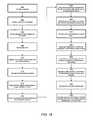
- FIG. 1is a side cross-sectional view of a silicon-containing substrate having a mask patterned thereon;
- FIG. 2is a side cross-sectional view of the silicon-containing substrate for FIG. 1 after etching to form fins;
- FIG. 3is a side cross-sectional view of structure of FIG. 2 after the removal of the mask
- FIG. 4is an oblique, cross-sectional view of the structure of FIG. 3 ;
- FIG. 5is a side cross-sectional view of the structure of FIGS. 3 and 4 after the deposition of a first dielectric material layer;
- FIG. 6is a side cross-sectional view of the structure of FIG. 5 after planarization of the first dielectric material layer;
- FIG. 7is a side cross-sectional view of the structure of FIG. 6 after recessing the first dielectric material layer to expose portions of the fins;
- FIG. 8is a side cross-sectional view of the structure of FIG. 7 after formation of a silicon germanium alloy cladding on exposed portions of the fins;
- FIG. 9is a side cross-sectional view of the structure of FIG. 8 after the formation of germanium nanowires
- FIG. 10is a side cross-sectional view of the structure of FIG. 9 after the deposition of a second dielectric material layer:
- FIG. 11is a side cross-sectional view of the structure of FIG. 10 after planarization of the second dielectric material layer;
- FIG. 12is a side cross-sectional view of the structure of FIG. 11 after the removal of the second dielectric material layer, which creates divot channels in the first dielectric material layer;
- FIG. 13is a side cross-sectional view of the structure of FIG. 12 after the deposition of a protective layer
- FIG. 14is a side cross-sectional view of the structure of FIG. 13 after the deposition of a filler dielectric material layer;
- FIG. 15is a side cross-sectional view of the structure of FIG. 14 after planarization of the filler dielectric material layer;
- FIG. 16is a side cross-sectional view of the structure of FIG. 15 after the partial removal of the filler dielectric material layer, wherein a portion of filler dielectric material layer remains in the divot channels;
- FIG. 17is an oblique, cross-sectional view of the structure of FIG. 16 ;
- FIG. 18is an oblique, cross-sectional view of a transistor gate with plurality of germanium nanowires as high mobility devices.
- FIG. 19is process flow of the fabrication of germanium nanowire.
- Embodiments of the present descriptionrelate to the fabrication of microelectronic devices.
- the present subject matterrelates to forming isolated a nanowire, wherein an isolation structure adjacent the nanowire provides a substantially level surface for the formation of microelectronic structures thereon.
- Microelectronic devicessuch as microprocessors, memory devices, and application specific integrated circuits, are formed from various electronic components, such as transistors, resistors, and capacitors, which are interconnected with traces to form circuits in and on microelectronic device wafers.
- the microelectronic device industryhas continuously strived to reduce the size of these components, which results in faster and less expensive microelectronic devices.
- problemsmay arise with regard to parasitic capacitance, off-state leakage, power consumption, and other performance characteristics of these microelectronic devices.
- transistorsparticularly metal oxide semiconductor field effect transistors
- performance and reliabilityhave been improved through the use of a variety of innovations such as the utilization of semiconductor-on-insulator substrates, the formation of selective epitaxially deposited raised source and drain, the formation of atomic layer deposited high-K gate dielectrics, the fabrication of metal gates, the formation of strained transistor channels, and the deposition of low-K interlevel dielectric layers.
- the channel length of the transistormay be reduced, as will be understood by those skilled in the art. This channel length reduction generally results in an increased device speed, as gate delay typically decreases. However, negative side effects may occur when the channel length is reduced, including but not limited to, increased off-state leakage current due to threshold voltage roll-off, also referred to as short channel effects.
- Carrier mobilityis generally a measure of the velocity at which carriers flow in a semiconductor material under an external unit electric field.
- carrier mobilityis a measure of the velocity at which carriers (e.g., electrons and holes) flow through or across a device channel in an inversion layer.
- structures and materials with higher mobility than that which can be delivered through the use of silicon alonemust be used.
- unique structures, such as high mobility nanowireshave been fabricated to serve as channels. Employing a nanowire as a channel of a transistor tends to yield a transistor having a low power consumption, a high integration degree, and a rapid response speed.
- nanowirescan be fabricated from a number of appropriate materials. However, it has been found that germanium can be conveniently formed into nanowires with techniques and machinery commonly used in the fabrication of integrated circuits. These germanium nanowires can be incorporated as high mobility transistor channels that are modulated by a gate in a transistor device to create logic, memory and low dimensional quantum transport devices. As devices continue to scale, the high mobility germanium nanowire devices may provide better control of short channel effects than silicon.
- FIG. 1illustrates a substrate 102 , having a mask 104 patterned thereon (see also blocks 202 and 204 of FIG. 19 ).
- the substrate 102may be a silicon-containing substrate, such as a mono-crystalline silicon wafer or any wafer or substrate having a high silicon content.
- the patterned mask 104may be a photoresist material patterned on a first surface 106 of the substrate 102 by various lithographic techniques known in the art, and may be patterned as an array of substantially parallel lines.
- the substrate 102may be anisotropically etched to form recesses 108 therein.
- the patterned mask 104blocks the etching thereby forming fins 112 .
- the each fin 112may include a top surface 114 and two opposing sides 116 , such that each fin has a height 122 and a wide 124 .
- the fin width 124may be between about 2 nm and 55 nm, and the fin height 122 between about 3 nm and 180 nm.
- the fins 112may be spaced (centerline to centerline) from between about 14 nm and 560 nm apart (not illustrated).
- the etching of the silicon-containing substrate 102may be achieved with a wet etch, including, but not limited to nitric acid/hydrofluoric acid solution, or a dry etch, including, but not limited to plasma etching with a sulfur hexafluoride gas, dichlorodifluoromethane gas, or the like.
- the patterned mask 104is removed.
- the removal of the patterned mask 104may be achieved with any known technique, including but not limited to chemical stripping and ashing (plasma in fluorine or oxygen).
- FIG. 4illustrates an oblique view of the structure of FIG. 3 to assist in understanding the shape of the fins 112 and to illustrate a length 126 of each fin 112 .
- the fin length 126may be between about 5 um and 25 um.
- a first dielectric material layer 128such as silicon oxide, may be formed over the recesses 108 and fins 112 , as shown in FIG. 5 and as set forth in block 210 of FIG. 19 .
- the first dielectric material layer 128may by deposited to completely fill the recesses and may have an excess amount deposited to ensure complete coverage.
- the first dielectric material layer 128may be deposited by any technique known in the art, including but not limited to, chemical vapor deposition, atomic layer deposition, physical vapor deposition, and the like.
- the first dielectric material layer 128may be planarized.
- the planarizationassists achieving an even and uniform etch in a subsequent step.
- the planarizationmay be achieved by technique known in the art, including but not limited to chemical mechanical polishing/planarization (“CMP”) and wet or dry etching.
- CMPchemical mechanical polishing/planarization
- the first dielectric material layer 128may be recessed (i.e., to a level lower that the fin top surface 114 ) to form a first surface 130 and to expose at least a portion of the fin sides 116 adjacent to the fin top surface 114 .
- Recessing the first dielectric material layer 128may be achieved by etching techniques known in the art. However, the etching technique may need to be selective relative to silicon or silicon-germanium, such that the fins 112 are not damaged by the recessing etch. In one embodiment, the recessing may be achieved with a wet etch using a dilute hydrofluoric acid solution.
- a silicon germanium alloy shell or cladding 132may be selectively formed over on each fin top surface 114 and exposed portions of the fin sides 116 , as shown in FIG. 8 and as set forth in block 216 of FIG. 19 .
- the silicon germanium alloy cladding 132may be formed with molecular beam epitaxy (“MBE”).
- the silicon germanium alloy cladding 132is formed with atomic layer deposition (“ALD”).
- the silicon germanium alloy cladding 132may be formed with metal-organic chemical vapor deposition (“MOCVD”).
- the silicon germanium alloy cladding 132may have a chemical formula of Si 1-x Ge x , where 0.05 ⁇ x ⁇ 0.35. In one embodiment of the present disclosure, the silicon germanium alloy cladding 132 may be intrinsic (undoped).
- the silicon germanium alloy cladding 132grows epitaxially along certain axes (or directions) that depend upon the surface orientation of a crystal lattice of the fin 112 proximate the fin top surface 114 and exposed fin sides 116 .
- the silicon germanium alloy claddingmay form to resemble a tilted cube (not shown), a roof-like structure (not shown), or a multiple 125-degree faceted structure (not shown).
- the silicon germanium alloy cladding 132is illustrated generically as semi-cylindrical, such that the cross-sectional view is semicircular.
- a germanium nanowire 134is then formed by an oxidation/anneal process.
- the oxidation/anneal processcomprises an oxidation step and the anneal step are performed at the same time (concurrent).
- the oxidation/anneal processcomprises an oxidation step followed by an anneal step (sequential).
- the oxidation/anneal processcomprises repeated, alternating oxidation steps and anneal steps performed to reach progressively higher germanium content within the germanium nanowire 134 , and to homogenize germanium content throughout the germanium nanowire 134 .
- the oxidation annealincludes a dry oxidation and an anneal performed, initially at about 1,050 degrees Centigrade to reach between about 60-65% germanium content within the germanium nanowire 134 , followed by an anneal at about 900 degrees Centigrade to reach between about 75-98% Germanium content within the germanium nanowire 134 .
- the oxidationmay be performed in dry (without water) oxygen mixed with a diluent gas or a carrier gas.
- the diluent gas or carrier gasis a non-oxidizing gas, such as nitrogen (N 2 ), or forming gas (H 2 /N 2 ).
- the diluent gas or carrier gasis an inert gas, such as argon (Ar), helium (He), and the like.
- the annealmay be performed in a sub-atmosphere or a partial vacuum.
- the oxidation/anneal processmay be performed at a temperature below a melting point of the silicon germanium alloy cladding 132 .
- the oxidation/anneal processis performed at a temperature of between about 840-1,065 degrees Centigrade. In yet another embodiment of the present disclosure, the oxidation/anneal process may be performed above a temperature at which viscous flow of silicon oxide will occur (about 950 degrees Centigrade).
- silicon and germaniumwill inter-diffuse depending on a concentration gradient and a thermal gradient, as will be understood to those skilled in the art.
- Siliconis thermally oxidized in a preferential manner over germanium at a thermal oxidation interface whenever sufficient quantities of silicon and germanium are available.
- performing the oxidation/anneal process on the silicon germanium alloy cladding 132results in diffusion of silicon towards the oxidation interface (i.e., outward) and condensing the germanium away from the oxidation interface (i.e., inward), thereby forming the germanium nanowire 134 and a silicon oxide shell 136 substantially surrounding the germanium nanowire 134 .
- the germanium nanowire 134may have a germanium content of between about 50% and 100%.
- the oxidation/anneal processmay turn a portion of the fin 112 closest to the germanium nanowire 134 to silicon oxide which decreases the fin height. However, depending on the oxidation/anneal process this may not occur.
- the present disclosurerelates to germanium nanowire, this is for exemplary purposes only, and the present disclosure is not so limited.
- the nanowiremay be fabricated from any appropriate material, particularly those materials which exhibit the migration/inter-diffuse properties of germanium and silicon, as will be understood to those skilled in the art.
- the germanium nanowire 134has a cross-sectional area that is substantially circular or oval, and thereby substantially cylindrical along its length. In an embodiment of the present invention, the germanium nanowire 134 may have an average diameter of between about 2 nm and 45 nm. In an embodiment of the present invention, the germanium nanowire 134 has a length of 5 um and 25 um. In an embodiment of the present invention, the germanium nanowire 134 has a diameter-to-length aspect ratio of between about 1:250 and 1:700.
- a second dielectric material layer 142may be deposited over the first dielectric material layer first surface 130 and the silicon oxide shell 136 .
- the second dielectric material layer 142may by deposited to completely fill the space between the silicon oxide shells 136 and may have an excess amount deposited to ensure complete coverage.
- the second dielectric material layer 142may be deposited by any technique known in the art, including but not limited to, chemical vapor deposition, atomic layer deposition, physical vapor deposition, and the like.
- the shape of the silicon oxide shell 136creates voids 144 , when the second dielectric material layer 142 is deposited.
- the second dielectric material layer 142may be planarized.
- the planarizationassists achieving an even and uniform etch in a subsequent step.
- the planarizationmay be achieved by technique known in the art, including but not limited to chemical mechanical polishing/planarization (“CMP”) and wet or dry etching.
- CMPchemical mechanical polishing/planarization
- the germanium nanowire 134is then exposed by etching the second dielectric material layer 142 and the silicon oxide shell 136 .
- Exposing the germanium nanowires 134may be achieved by etching techniques known in the art. However, the etching technique should be selective relative to germanium, such that the germanium nanowires 134 are not damaged by the etching. In one embodiment, the recessing may be achieved with a wet etch using a hydrofluoric acid solution.
- the voids 144(see FIG. 11 ) that were formed during the deposition of the second dielectric material layer 142 cause uneven etching when the first dielectric material layer 128 is exposed.
- the uneven etchingmay result in the shape of the voids 144 being translated into the first dielectric material layer 128 , thereby forming divot channels 146 extending into the first dielectric material 128 from the first dielectric material first surface 130 .
- These divot channels 146can be over 300 angstroms deep.
- the divot channels 146would trap gate materials of a gate structure formed over the germanium nanowire 134 , as will be understood to those skilled in the art. Further, the elimination of the divot channels 146 to successfully pattern a gate structure would require significant over-etching which may notch or undercut a top gate of a subsequently formed transistor gate structure, as will be understood by those skilled in the art.
- a protective layer 152may be deposited over the germanium nanowires 134 , over the first dielectric material layer first surface 130 , and in the divot channels 146 , as shown in FIG. 13 and as set forth in block 226 of FIG. 19 .
- the protective layer 152may be a silicon nitride dielectric layer or a high-K dielectric material, including but not limited to hafnium silicate, zirconium silicate, hafnium dioxide, and zirconium dioxide. If the protective layer 152 is a silicon nitride dielectric layer, it will be removed prior to the fabrication of a gate structure (not shown).
- the protective layer 152is a high-K dielectric material, it can be left on and the gate structure (not shown) fabricated thereon.
- the protective layer 152may be deposited by a conformal deposition technique, including, but not limited to physical vapor deposition, chemical vapor deposition, plasma enhanced chemical vapor deposition, and atomic layer deposition.
- a filler dielectric material layer 154may be deposited over the protective layer 152 .
- the filler dielectric material layer 154may by deposited to completely fill the space between the germanium nanowires 134 and may have an excess amount deposited to ensure complete coverage.
- the filler dielectric material layer 154may be deposited by any technique known in the art, including but not limited to, chemical vapor deposition, atomic layer deposition, physical vapor deposition, and the like.
- the filler dielectric material layer 154may be planarized.
- the planarizationassists achieving an even and uniform etch in a subsequent step.
- the planarizationmay be achieved by technique known in the art, including but not limited to chemical mechanical polishing/planarization (“CMP”) and wet or dry etching.
- CMPchemical mechanical polishing/planarization
- the protective layer 152is then substantially exposed by etching the filler dielectric material layer 154 , while leaving a portions 156 of the filler dielectric material layer 154 within the divot channels 146 (see FIG. 13 ).
- the filler dielectric material layer portion 156may be substantially planar to the protective layer 152 , which results in a substantially level isolation structure 160 between the germanium nanowires 134 , upon which a gate structure (not shown) can be fabricated.
- Exposing the protective layer 152may be achieved by etching techniques known in the art. However, the etching technique will need to be selective relative to protective layer 152 . In one embodiment, exposing the protective layer 152 may be achieved with a wet etch. In an embodiment, the protective layer 152 is silicon nitride and the etching solution is hydrofluoric acid based.
- FIG. 17is an oblique view of the isolation structure 160 as shown in FIG. 18 .
- FIG. 18is an oblique view of the structure of FIG. 17 having a gate structure 162 formed over the germanium nanowires 134 , such that the germanium nanowires 134 act as high mobility channels for a transistor, as will be understood to those skilled in the art.
- the gate structure 162is shown generically, as those skilled in the art are aware of the various ways in which the gate structure 162 may be structured and formed.
- the present disclosureis not so limited.
- the present disclosureis applicable to a single nanowire being formed, wherein the first dielectric material, the second dielectric material, protective layer, and/or filler material are deposited adjacent and/or on the nanowire, cladding, and/or fin.
- the present disclosureis also application to numerous nanowires being formed simultaneously.
- any two components herein combined to achieve a particular functionalitycan be seen as “associated with” each other such that the desired functionality is achieved, irrespective of structures or intermediate components.
- any two components so associatedcan also be viewed as being “operably connected”, or “operably coupled”, to each other to achieve the desired functionality, and any two components capable of being so associated can also be viewed as being “operably couplable”, to each other to achieve the desired functionality.
- operably couplableinclude but are not limited to physically mateable and/or physically interacting components and/or wirelessly interactable and/or wirelessly interacting components and/or logically interacting and/or logically interactable components.
- an embodimentmay mean that a particular feature, structure, or characteristic described in connection with one or more embodiments may be included in at least some embodiments, but not necessarily in all embodiments.
- the various uses of the terms “an embodiment,” “one embodiment,” “another embodiment,” or “other embodiments” in the detailed descriptionare not necessarily all referring to the same embodiments.
Landscapes
- Engineering & Computer Science (AREA)
- Chemical & Material Sciences (AREA)
- Physics & Mathematics (AREA)
- Nanotechnology (AREA)
- Manufacturing & Machinery (AREA)
- General Physics & Mathematics (AREA)
- Condensed Matter Physics & Semiconductors (AREA)
- Computer Hardware Design (AREA)
- Microelectronics & Electronic Packaging (AREA)
- Power Engineering (AREA)
- Crystallography & Structural Chemistry (AREA)
- Mathematical Physics (AREA)
- Theoretical Computer Science (AREA)
- Insulated Gate Type Field-Effect Transistor (AREA)
- Thin Film Transistor (AREA)
- Metal-Oxide And Bipolar Metal-Oxide Semiconductor Integrated Circuits (AREA)
- Silicon Compounds (AREA)
- Materials Engineering (AREA)
Abstract
Description
Claims (18)
Priority Applications (8)
| Application Number | Priority Date | Filing Date | Title |
|---|---|---|---|
| US12/653,847US8269209B2 (en) | 2009-12-18 | 2009-12-18 | Isolation for nanowire devices |
| PCT/US2010/055225WO2011075228A2 (en) | 2009-12-18 | 2010-11-03 | Isolation for nanowire devices |
| EP10838069.2AEP2513972B1 (en) | 2009-12-18 | 2010-11-03 | Isolation for nanowire devices |
| CN201080057647.8ACN102652364B (en) | 2009-12-18 | 2010-11-03 | For the isolation of nano-wire devices |
| HK13102339.1AHK1175029B (en) | 2009-12-18 | 2010-11-03 | Isolation for nanowire devices |
| KR1020127016670AKR101384394B1 (en) | 2009-12-18 | 2010-11-03 | Isolation for nanowire devices |
| JP2012543109AJP5497193B2 (en) | 2009-12-18 | 2010-11-03 | Nanowire insulation structure and formation method |
| US13/563,456US8883573B2 (en) | 2009-12-18 | 2012-07-31 | Isolation for nanowire devices |
Applications Claiming Priority (1)
| Application Number | Priority Date | Filing Date | Title |
|---|---|---|---|
| US12/653,847US8269209B2 (en) | 2009-12-18 | 2009-12-18 | Isolation for nanowire devices |
Related Child Applications (1)
| Application Number | Title | Priority Date | Filing Date |
|---|---|---|---|
| US13/563,456DivisionUS8883573B2 (en) | 2009-12-18 | 2012-07-31 | Isolation for nanowire devices |
Publications (2)
| Publication Number | Publication Date |
|---|---|
| US20110147697A1 US20110147697A1 (en) | 2011-06-23 |
| US8269209B2true US8269209B2 (en) | 2012-09-18 |
Family
ID=44149774
Family Applications (2)
| Application Number | Title | Priority Date | Filing Date |
|---|---|---|---|
| US12/653,847Expired - Fee RelatedUS8269209B2 (en) | 2009-12-18 | 2009-12-18 | Isolation for nanowire devices |
| US13/563,456Active2030-05-28US8883573B2 (en) | 2009-12-18 | 2012-07-31 | Isolation for nanowire devices |
Family Applications After (1)
| Application Number | Title | Priority Date | Filing Date |
|---|---|---|---|
| US13/563,456Active2030-05-28US8883573B2 (en) | 2009-12-18 | 2012-07-31 | Isolation for nanowire devices |
Country Status (6)
| Country | Link |
|---|---|
| US (2) | US8269209B2 (en) |
| EP (1) | EP2513972B1 (en) |
| JP (1) | JP5497193B2 (en) |
| KR (1) | KR101384394B1 (en) |
| CN (1) | CN102652364B (en) |
| WO (1) | WO2011075228A2 (en) |
Cited By (4)
| Publication number | Priority date | Publication date | Assignee | Title |
|---|---|---|---|---|
| US8883573B2 (en) | 2009-12-18 | 2014-11-11 | Intel Corporation | Isolation for nanowire devices |
| US9496263B1 (en)* | 2015-10-23 | 2016-11-15 | International Business Machines Corporation | Stacked strained and strain-relaxed hexagonal nanowires |
| US9508834B1 (en) | 2015-08-28 | 2016-11-29 | United Microelectronics Corp. | Semiconductor device and method for fabricating the same |
| US9583627B2 (en) | 2015-06-09 | 2017-02-28 | United Microelectronics Corp. | Semiconductor device and method for fabricating the same |
Families Citing this family (27)
| Publication number | Priority date | Publication date | Assignee | Title |
|---|---|---|---|---|
| US7821061B2 (en) | 2007-03-29 | 2010-10-26 | Intel Corporation | Silicon germanium and germanium multigate and nanowire structures for logic and multilevel memory applications |
| KR101539669B1 (en)* | 2008-12-16 | 2015-07-27 | 삼성전자주식회사 | Method for forming a core-shell type structure and method for manufacturing a transistor using the same |
| US8580634B1 (en)* | 2012-09-11 | 2013-11-12 | Globalfoundries Inc. | Methods of forming 3-D semiconductor devices with a nanowire gate structure wherein the nanowire gate structure is formed prior to source/drain formation |
| EP2709156A3 (en)* | 2012-09-14 | 2014-04-23 | Imec | Band engineered semiconductor device and method for manufacturing thereof |
| US8957476B2 (en)* | 2012-12-20 | 2015-02-17 | Intel Corporation | Conversion of thin transistor elements from silicon to silicon germanium |
| US9391181B2 (en)* | 2012-12-21 | 2016-07-12 | Intel Corporation | Lattice mismatched hetero-epitaxial film |
| US8853019B1 (en) | 2013-03-13 | 2014-10-07 | Globalfoundries Inc. | Methods of forming a semiconductor device with a nanowire channel structure by performing an anneal process |
| US9035277B2 (en)* | 2013-08-01 | 2015-05-19 | Taiwan Semiconductor Manufacturing Company, Ltd. | Semiconductor device and fabricating the same |
| EP3050111A4 (en)* | 2013-09-27 | 2017-06-07 | Intel Corporation | Improved cladding layer epitaxy via template engineering for heterogeneous integration on silicon |
| US9331146B2 (en)* | 2014-06-11 | 2016-05-03 | International Business Machines Corporation | Silicon nanowire formation in replacement metal gate process |
| US9431512B2 (en) | 2014-06-18 | 2016-08-30 | Globalfoundries Inc. | Methods of forming nanowire devices with spacers and the resulting devices |
| US9490340B2 (en) | 2014-06-18 | 2016-11-08 | Globalfoundries Inc. | Methods of forming nanowire devices with doped extension regions and the resulting devices |
| KR102236049B1 (en)* | 2014-07-07 | 2021-04-05 | 삼성전자주식회사 | Semiconductor device and method for fabricating the same |
| TWI531071B (en)* | 2014-07-08 | 2016-04-21 | Univ Nat Central | Fabrication method of gold - oxygen half - gate stacking structure |
| US9698025B2 (en)* | 2014-09-04 | 2017-07-04 | Globalfoundries Inc. | Directed self-assembly material growth mask for forming vertical nanowires |
| US9437699B2 (en)* | 2014-10-03 | 2016-09-06 | Taiwan Semiconductor Manufacturing Company Limited | Method of forming nanowires |
| US9543441B2 (en)* | 2015-03-11 | 2017-01-10 | Globalfoundries Inc. | Methods, apparatus and system for fabricating high performance finFET device |
| US9786976B2 (en)* | 2015-06-24 | 2017-10-10 | Taiwan Semiconductor Manufacturing Company, Ltd. | Transmission line design and method, where high-k dielectric surrounds the transmission line for increased isolation |
| CN105047701A (en)* | 2015-06-30 | 2015-11-11 | 上海华力微电子有限公司 | Method for preparing fin-shaped semiconductor device with suspended grid electrode |
| US9570299B1 (en)* | 2015-09-08 | 2017-02-14 | International Business Machines Corporation | Formation of SiGe nanotubes |
| EP3353810A4 (en)* | 2015-09-25 | 2019-05-01 | Intel Corporation | PASSIVATION OF TRANSISTOR CHANNEL ZONE INTERFACES |
| CN106856208B (en)* | 2015-12-08 | 2019-09-27 | 中芯国际集成电路制造(北京)有限公司 | Nanowire semiconductor device and method of forming the same |
| US9425293B1 (en)* | 2015-12-30 | 2016-08-23 | International Business Machines Corporation | Stacked nanowires with multi-threshold voltage solution for pFETs |
| US11594637B2 (en)* | 2020-03-27 | 2023-02-28 | Intel Corporation | Gate-all-around integrated circuit structures having fin stack isolation |
| DE102020131030A1 (en)* | 2020-05-12 | 2021-11-18 | Taiwan Semiconductor Manufacturing Co., Ltd. | SILICON CHANNEL STARTING |
| CN111613536A (en)* | 2020-05-29 | 2020-09-01 | 上海华力集成电路制造有限公司 | A fin-type semiconductor device and its manufacturing method |
| CN114613676A (en)* | 2020-12-09 | 2022-06-10 | 清华大学 | Field effect transistor and method of making the same |
Citations (11)
| Publication number | Priority date | Publication date | Assignee | Title |
|---|---|---|---|---|
| US20040065930A1 (en)* | 2001-10-18 | 2004-04-08 | Chartered Semiconductor Manufacturing, Ltd. | Dual metal gate process: metals and their silicides |
| US20050136585A1 (en) | 2003-12-23 | 2005-06-23 | Chau Robert S. | Method of fabricating semiconductor devices with replacement, coaxial gate structure |
| US20070145375A1 (en)* | 2005-12-28 | 2007-06-28 | Cho Hans S | Method of manufacturing nanowire, method of manufacturing a semiconductor apparatus including nanowire and semiconductor apparatus formed from the same |
| US20080224122A1 (en)* | 2004-12-28 | 2008-09-18 | Tohru Saitoh | Semiconductor Nanowire and Semiconductor Device Including the Nanowire |
| US20080237575A1 (en) | 2007-03-29 | 2008-10-02 | Been-Yih Jin | Silicon germanium and germanium multigate and nanowire structures for logic and multilevel memory applications |
| US20080237684A1 (en)* | 2007-03-26 | 2008-10-02 | Michael Specht | Method of manufacturing a nanowire transistor, a nanowire transistor structure, a nanowire transistor field |
| US7446025B2 (en)* | 2005-05-23 | 2008-11-04 | International Business Machines Corporation | Method of forming vertical FET with nanowire channels and a silicided bottom contact |
| US20090061568A1 (en) | 2007-09-05 | 2009-03-05 | International Business Machines Corporation | Techniques for Fabricating Nanowire Field-Effect Transistors |
| US20090170251A1 (en) | 2007-12-31 | 2009-07-02 | Been-Yih Jin | Fabrication of germanium nanowire transistors |
| US20090200536A1 (en)* | 2004-06-30 | 2009-08-13 | Koninklijke Philips Electronics N.V. | Method for manufacturing an electric device with a layer of conductive material contracted by nanowire |
| WO2011075228A2 (en) | 2009-12-18 | 2011-06-23 | Intel Corporation | Isolation for nanowire devices |
Family Cites Families (12)
| Publication number | Priority date | Publication date | Assignee | Title |
|---|---|---|---|---|
| CN1202570C (en)* | 2001-11-08 | 2005-05-18 | 旺宏电子股份有限公司 | A shallow trench insulation process method |
| CN1449012A (en)* | 2002-03-29 | 2003-10-15 | 旺宏电子股份有限公司 | A Method of Improving the Reliability of Shallow Trench Isolation |
| US6855990B2 (en)* | 2002-11-26 | 2005-02-15 | Taiwan Semiconductor Manufacturing Co., Ltd | Strained-channel multiple-gate transistor |
| KR100634372B1 (en)* | 2004-06-04 | 2006-10-16 | 삼성전자주식회사 | Semiconductor Devices and Formation Methods |
| US7989855B2 (en)* | 2004-06-10 | 2011-08-02 | Nec Corporation | Semiconductor device including a deflected part |
| WO2006038504A1 (en)* | 2004-10-04 | 2006-04-13 | Matsushita Electric Industrial Co., Ltd. | Vertical field effect transistor and method for making the same |
| JP4635897B2 (en)* | 2006-02-15 | 2011-02-23 | 株式会社東芝 | Semiconductor device and manufacturing method thereof |
| JP2009535800A (en)* | 2006-04-26 | 2009-10-01 | エヌエックスピー ビー ヴィ | Nonvolatile memory device |
| JP2008172082A (en)* | 2007-01-12 | 2008-07-24 | Toshiba Corp | Semiconductor device and manufacturing method of semiconductor device |
| CN101330035B (en)* | 2007-06-18 | 2010-05-19 | 中芯国际集成电路制造(上海)有限公司 | Isolation structure of shallow plough groove and manufacturing method thereof |
| US7767560B2 (en)* | 2007-09-29 | 2010-08-03 | Intel Corporation | Three dimensional strained quantum wells and three dimensional strained surface channels by Ge confinement method |
| US8999851B2 (en)* | 2007-12-14 | 2015-04-07 | Oned Material Llc | Methods for formation of substrate elements |
- 2009
- 2009-12-18USUS12/653,847patent/US8269209B2/ennot_activeExpired - Fee Related
- 2010
- 2010-11-03EPEP10838069.2Apatent/EP2513972B1/enactiveActive
- 2010-11-03JPJP2012543109Apatent/JP5497193B2/enactiveActive
- 2010-11-03WOPCT/US2010/055225patent/WO2011075228A2/enactiveApplication Filing
- 2010-11-03CNCN201080057647.8Apatent/CN102652364B/ennot_activeExpired - Fee Related
- 2010-11-03KRKR1020127016670Apatent/KR101384394B1/enactiveActive
- 2012
- 2012-07-31USUS13/563,456patent/US8883573B2/enactiveActive
Patent Citations (11)
| Publication number | Priority date | Publication date | Assignee | Title |
|---|---|---|---|---|
| US20040065930A1 (en)* | 2001-10-18 | 2004-04-08 | Chartered Semiconductor Manufacturing, Ltd. | Dual metal gate process: metals and their silicides |
| US20050136585A1 (en) | 2003-12-23 | 2005-06-23 | Chau Robert S. | Method of fabricating semiconductor devices with replacement, coaxial gate structure |
| US20090200536A1 (en)* | 2004-06-30 | 2009-08-13 | Koninklijke Philips Electronics N.V. | Method for manufacturing an electric device with a layer of conductive material contracted by nanowire |
| US20080224122A1 (en)* | 2004-12-28 | 2008-09-18 | Tohru Saitoh | Semiconductor Nanowire and Semiconductor Device Including the Nanowire |
| US7446025B2 (en)* | 2005-05-23 | 2008-11-04 | International Business Machines Corporation | Method of forming vertical FET with nanowire channels and a silicided bottom contact |
| US20070145375A1 (en)* | 2005-12-28 | 2007-06-28 | Cho Hans S | Method of manufacturing nanowire, method of manufacturing a semiconductor apparatus including nanowire and semiconductor apparatus formed from the same |
| US20080237684A1 (en)* | 2007-03-26 | 2008-10-02 | Michael Specht | Method of manufacturing a nanowire transistor, a nanowire transistor structure, a nanowire transistor field |
| US20080237575A1 (en) | 2007-03-29 | 2008-10-02 | Been-Yih Jin | Silicon germanium and germanium multigate and nanowire structures for logic and multilevel memory applications |
| US20090061568A1 (en) | 2007-09-05 | 2009-03-05 | International Business Machines Corporation | Techniques for Fabricating Nanowire Field-Effect Transistors |
| US20090170251A1 (en) | 2007-12-31 | 2009-07-02 | Been-Yih Jin | Fabrication of germanium nanowire transistors |
| WO2011075228A2 (en) | 2009-12-18 | 2011-06-23 | Intel Corporation | Isolation for nanowire devices |
Non-Patent Citations (1)
| Title |
|---|
| International Search Report and Written Opinion received for PCT Patent Application No. PCT/US2010/055225, mailed on Jul. 1, 2011, 8 pages. |
Cited By (7)
| Publication number | Priority date | Publication date | Assignee | Title |
|---|---|---|---|---|
| US8883573B2 (en) | 2009-12-18 | 2014-11-11 | Intel Corporation | Isolation for nanowire devices |
| US9583627B2 (en) | 2015-06-09 | 2017-02-28 | United Microelectronics Corp. | Semiconductor device and method for fabricating the same |
| US9837511B2 (en) | 2015-06-09 | 2017-12-05 | United Microelectronics Corp. | Method for fabricating semiconductor device |
| US9508834B1 (en) | 2015-08-28 | 2016-11-29 | United Microelectronics Corp. | Semiconductor device and method for fabricating the same |
| US9496263B1 (en)* | 2015-10-23 | 2016-11-15 | International Business Machines Corporation | Stacked strained and strain-relaxed hexagonal nanowires |
| US9761661B2 (en) | 2015-10-23 | 2017-09-12 | International Business Machines Corporation | Stacked strained and strain-relaxed hexagonal nanowires |
| US9859367B2 (en) | 2015-10-23 | 2018-01-02 | International Business Machines Corporation | Stacked strained and strain-relaxed hexagonal nanowires |
Also Published As
| Publication number | Publication date |
|---|---|
| CN102652364B (en) | 2015-09-30 |
| JP2013513249A (en) | 2013-04-18 |
| CN102652364A (en) | 2012-08-29 |
| EP2513972A2 (en) | 2012-10-24 |
| US8883573B2 (en) | 2014-11-11 |
| KR20120087999A (en) | 2012-08-07 |
| WO2011075228A2 (en) | 2011-06-23 |
| EP2513972A4 (en) | 2015-03-11 |
| US20120309173A1 (en) | 2012-12-06 |
| EP2513972B1 (en) | 2016-05-04 |
| HK1175029A1 (en) | 2013-06-21 |
| US20110147697A1 (en) | 2011-06-23 |
| JP5497193B2 (en) | 2014-05-21 |
| WO2011075228A3 (en) | 2011-08-25 |
| KR101384394B1 (en) | 2014-04-10 |
Similar Documents
| Publication | Publication Date | Title |
|---|---|---|
| US8269209B2 (en) | Isolation for nanowire devices | |
| US11239341B2 (en) | Horizontal gate all-around device having wrapped-around source and drain | |
| KR102073395B1 (en) | A method of manufacturing a semiconductor device with separated merged source/drain structure | |
| US8536029B1 (en) | Nanowire FET and finFET | |
| TWI567981B (en) | Fin member structure and manufacturing method thereof | |
| US10546785B2 (en) | Method to recess cobalt for gate metal application | |
| CN112563266A (en) | Semiconductor device with a plurality of semiconductor chips | |
| TW201829293A (en) | Semiconductor component | |
| KR20180138104A (en) | Isolation manufacturing method for semiconductor structures | |
| US9425053B2 (en) | Block mask litho on high aspect ratio topography with minimal semiconductor material damage | |
| JP7559202B2 (en) | Selective silicon etching for gate-all-around transistors. | |
| KR20170073644A (en) | Methods and apparatus for forming horizontal gate all around device structures | |
| CN106548944A (en) | Method for manufacturing semiconductor device | |
| US9496259B2 (en) | FinFET semiconductor device having fins with stronger structural strength | |
| US10211225B2 (en) | FinFET devices wit multiple channel lengths | |
| TWI656638B (en) | Method and structure for iii-v nanowire tunnel fets | |
| CN110970489A (en) | Semiconductor device and method of forming a semiconductor device | |
| CN109950311B (en) | Semiconductor structure and forming method thereof | |
| US11145760B2 (en) | Structure having improved fin critical dimension control | |
| CN106898553A (en) | A kind of fin formula field effect transistor and preparation method thereof | |
| HK1175029B (en) | Isolation for nanowire devices | |
| CN118661251A (en) | Gate wrap-around backside power rail with diffusion interrupt | |
| CN117836948A (en) | Source-drain formation in gate-all-around transistors |
Legal Events
| Date | Code | Title | Description |
|---|---|---|---|
| AS | Assignment | Owner name:INTEL CORPORATION, CALIFORNIA Free format text:ASSIGNMENT OF ASSIGNORS INTEREST;ASSIGNORS:SHAH, UDAY;CHU-KUNG, BENJAMIN;JIN, BEEN-YIH;AND OTHERS;REEL/FRAME:026666/0335 Effective date:20091217 | |
| FEPP | Fee payment procedure | Free format text:PAYOR NUMBER ASSIGNED (ORIGINAL EVENT CODE: ASPN); ENTITY STATUS OF PATENT OWNER: LARGE ENTITY | |
| ZAAA | Notice of allowance and fees due | Free format text:ORIGINAL CODE: NOA | |
| ZAAB | Notice of allowance mailed | Free format text:ORIGINAL CODE: MN/=. | |
| STCF | Information on status: patent grant | Free format text:PATENTED CASE | |
| CC | Certificate of correction | ||
| FPAY | Fee payment | Year of fee payment:4 | |
| MAFP | Maintenance fee payment | Free format text:PAYMENT OF MAINTENANCE FEE, 8TH YEAR, LARGE ENTITY (ORIGINAL EVENT CODE: M1552); ENTITY STATUS OF PATENT OWNER: LARGE ENTITY Year of fee payment:8 | |
| AS | Assignment | Owner name:GOOGLE LLC, CALIFORNIA Free format text:ASSIGNMENT OF ASSIGNORS INTEREST;ASSIGNOR:INTEL CORPORATION;REEL/FRAME:054772/0918 Effective date:20201113 | |
| FEPP | Fee payment procedure | Free format text:MAINTENANCE FEE REMINDER MAILED (ORIGINAL EVENT CODE: REM.); ENTITY STATUS OF PATENT OWNER: LARGE ENTITY | |
| LAPS | Lapse for failure to pay maintenance fees | Free format text:PATENT EXPIRED FOR FAILURE TO PAY MAINTENANCE FEES (ORIGINAL EVENT CODE: EXP.); ENTITY STATUS OF PATENT OWNER: LARGE ENTITY | |
| STCH | Information on status: patent discontinuation | Free format text:PATENT EXPIRED DUE TO NONPAYMENT OF MAINTENANCE FEES UNDER 37 CFR 1.362 | |
| FP | Lapsed due to failure to pay maintenance fee | Effective date:20240918 |