US8268646B2 - Group III-nitrides on SI substrates using a nanostructured interlayer - Google Patents
Group III-nitrides on SI substrates using a nanostructured interlayerDownload PDFInfo
- Publication number
- US8268646B2 US8268646B2US12/257,567US25756708AUS8268646B2US 8268646 B2US8268646 B2US 8268646B2US 25756708 AUS25756708 AUS 25756708AUS 8268646 B2US8268646 B2US 8268646B2
- Authority
- US
- United States
- Prior art keywords
- group iii
- interlayer
- gan
- nitride layer
- highly textured
- Prior art date
- Legal status (The legal status is an assumption and is not a legal conclusion. Google has not performed a legal analysis and makes no representation as to the accuracy of the status listed.)
- Expired - Fee Related
Links
- 239000000758substrateSubstances0.000titleclaimsabstractdescription62
- 239000011229interlayerSubstances0.000titleclaimsabstractdescription43
- 239000010410layerSubstances0.000claimsabstractdescription56
- 238000000151depositionMethods0.000claimsabstractdescription31
- 229910052710siliconInorganic materials0.000claimsabstractdescription27
- XUIMIQQOPSSXEZ-UHFFFAOYSA-NSiliconChemical compound[Si]XUIMIQQOPSSXEZ-UHFFFAOYSA-N0.000claimsabstractdescription26
- 238000000034methodMethods0.000claimsabstractdescription26
- 239000010703siliconSubstances0.000claimsabstractdescription26
- 229910021421monocrystalline siliconInorganic materials0.000claimsabstractdescription9
- 238000007373indentationMethods0.000claimsabstractdescription5
- 239000002073nanorodSubstances0.000claimsdescription46
- 230000008021depositionEffects0.000claimsdescription15
- 238000000354decomposition reactionMethods0.000claimsdescription4
- 150000004767nitridesChemical class0.000claims2
- 239000013078crystalSubstances0.000description10
- IBEFSUTVZWZJEL-UHFFFAOYSA-NtrimethylindiumChemical compoundC[In](C)CIBEFSUTVZWZJEL-UHFFFAOYSA-N0.000description10
- VYPSYNLAJGMNEJ-UHFFFAOYSA-NSilicium dioxideChemical compoundO=[Si]=OVYPSYNLAJGMNEJ-UHFFFAOYSA-N0.000description9
- VEXZGXHMUGYJMC-UHFFFAOYSA-NHydrochloric acidChemical compoundClVEXZGXHMUGYJMC-UHFFFAOYSA-N0.000description6
- 238000005336crackingMethods0.000description6
- IXCSERBJSXMMFS-UHFFFAOYSA-Nhydrogen chlorideSubstancesCl.ClIXCSERBJSXMMFS-UHFFFAOYSA-N0.000description6
- 229910000041hydrogen chlorideInorganic materials0.000description6
- QGZKDVFQNNGYKY-UHFFFAOYSA-NAmmoniaChemical compoundNQGZKDVFQNNGYKY-UHFFFAOYSA-N0.000description5
- 238000001816coolingMethods0.000description5
- 238000001228spectrumMethods0.000description5
- 230000008901benefitEffects0.000description4
- PSCMQHVBLHHWTO-UHFFFAOYSA-Kindium(iii) chlorideChemical compoundCl[In](Cl)ClPSCMQHVBLHHWTO-UHFFFAOYSA-K0.000description4
- 238000001878scanning electron micrographMethods0.000description4
- 239000000377silicon dioxideSubstances0.000description4
- RGGPNXQUMRMPRA-UHFFFAOYSA-NtriethylgalliumChemical groupCC[Ga](CC)CCRGGPNXQUMRMPRA-UHFFFAOYSA-N0.000description4
- 235000012431wafersNutrition0.000description4
- CSCPPACGZOOCGX-UHFFFAOYSA-NAcetoneChemical compoundCC(C)=OCSCPPACGZOOCGX-UHFFFAOYSA-N0.000description3
- OKKJLVBELUTLKV-UHFFFAOYSA-NMethanolChemical compoundOCOKKJLVBELUTLKV-UHFFFAOYSA-N0.000description3
- 238000000137annealingMethods0.000description3
- 238000005530etchingMethods0.000description3
- 239000000463materialSubstances0.000description3
- 238000002488metal-organic chemical vapour depositionMethods0.000description3
- 229910000069nitrogen hydrideInorganic materials0.000description3
- 239000002243precursorSubstances0.000description3
- 235000012239silicon dioxideNutrition0.000description3
- 229910002704AlGaNInorganic materials0.000description2
- IJGRMHOSHXDMSA-UHFFFAOYSA-NAtomic nitrogenChemical compoundN#NIJGRMHOSHXDMSA-UHFFFAOYSA-N0.000description2
- OKTJSMMVPCPJKN-UHFFFAOYSA-NCarbonChemical compound[C]OKTJSMMVPCPJKN-UHFFFAOYSA-N0.000description2
- -1Epichem)Chemical compound0.000description2
- 229910001199N alloyInorganic materials0.000description2
- 229910008045Si-SiInorganic materials0.000description2
- 229910006411Si—SiInorganic materials0.000description2
- QVGXLLKOCUKJST-UHFFFAOYSA-Natomic oxygenChemical compound[O]QVGXLLKOCUKJST-UHFFFAOYSA-N0.000description2
- 230000015572biosynthetic processEffects0.000description2
- 239000012159carrier gasSubstances0.000description2
- 239000003153chemical reaction reagentSubstances0.000description2
- 229910052681coesiteInorganic materials0.000description2
- 229910052906cristobaliteInorganic materials0.000description2
- 238000002474experimental methodMethods0.000description2
- 235000019589hardnessNutrition0.000description2
- 238000011065in-situ storageMethods0.000description2
- 238000004519manufacturing processMethods0.000description2
- 230000006911nucleationEffects0.000description2
- 238000010899nucleationMethods0.000description2
- 239000001301oxygenSubstances0.000description2
- 229910052760oxygenInorganic materials0.000description2
- 239000004065semiconductorSubstances0.000description2
- 238000000926separation methodMethods0.000description2
- 229910052682stishoviteInorganic materials0.000description2
- 229910052905tridymiteInorganic materials0.000description2
- 229910018509Al—NInorganic materials0.000description1
- 229910007991Si-NInorganic materials0.000description1
- 229910006294Si—NInorganic materials0.000description1
- XSTXAVWGXDQKEL-UHFFFAOYSA-NTrichloroethyleneChemical groupClC=C(Cl)ClXSTXAVWGXDQKEL-UHFFFAOYSA-N0.000description1
- 229910021529ammoniaInorganic materials0.000description1
- 238000013459approachMethods0.000description1
- 238000009835boilingMethods0.000description1
- 229910052799carbonInorganic materials0.000description1
- 239000002041carbon nanotubeSubstances0.000description1
- 229910021393carbon nanotubeInorganic materials0.000description1
- 238000004581coalescenceMethods0.000description1
- 230000007547defectEffects0.000description1
- 238000011161developmentMethods0.000description1
- 238000010586diagramMethods0.000description1
- 230000000694effectsEffects0.000description1
- 238000000724energy-dispersive X-ray spectrumMethods0.000description1
- 239000007789gasSubstances0.000description1
- 238000010438heat treatmentMethods0.000description1
- 238000001534heteroepitaxyMethods0.000description1
- 238000002248hydride vapour-phase epitaxyMethods0.000description1
- 229910052738indiumInorganic materials0.000description1
- APFVFJFRJDLVQX-UHFFFAOYSA-Nindium atomChemical compound[In]APFVFJFRJDLVQX-UHFFFAOYSA-N0.000description1
- 230000000873masking effectEffects0.000description1
- 229910052751metalInorganic materials0.000description1
- 239000002184metalSubstances0.000description1
- 229910052757nitrogenInorganic materials0.000description1
- 230000003287optical effectEffects0.000description1
- 230000035515penetrationEffects0.000description1
- 239000010453quartzSubstances0.000description1
- 238000009877renderingMethods0.000description1
- 238000011160researchMethods0.000description1
- 229910052594sapphireInorganic materials0.000description1
- 239000010980sapphireSubstances0.000description1
- 238000012216screeningMethods0.000description1
- 239000006104solid solutionSubstances0.000description1
- 239000000243solutionSubstances0.000description1
- UBOXGVDOUJQMTN-UHFFFAOYSA-NtrichloroethyleneNatural productsClCC(Cl)ClUBOXGVDOUJQMTN-UHFFFAOYSA-N0.000description1
- XLYOFNOQVPJJNP-UHFFFAOYSA-NwaterChemical compoundOXLYOFNOQVPJJNP-UHFFFAOYSA-N0.000description1
Images


Classifications
- H—ELECTRICITY
- H01—ELECTRIC ELEMENTS
- H01L—SEMICONDUCTOR DEVICES NOT COVERED BY CLASS H10
- H01L21/00—Processes or apparatus adapted for the manufacture or treatment of semiconductor or solid state devices or of parts thereof
- H01L21/02—Manufacture or treatment of semiconductor devices or of parts thereof
- H01L21/02104—Forming layers
- H01L21/02365—Forming inorganic semiconducting materials on a substrate
- H01L21/02656—Special treatments
- H01L21/02658—Pretreatments
- H—ELECTRICITY
- H01—ELECTRIC ELEMENTS
- H01L—SEMICONDUCTOR DEVICES NOT COVERED BY CLASS H10
- H01L21/00—Processes or apparatus adapted for the manufacture or treatment of semiconductor or solid state devices or of parts thereof
- H01L21/02—Manufacture or treatment of semiconductor devices or of parts thereof
- H01L21/02104—Forming layers
- H01L21/02365—Forming inorganic semiconducting materials on a substrate
- H01L21/02367—Substrates
- H01L21/0237—Materials
- H01L21/02373—Group 14 semiconducting materials
- H01L21/02381—Silicon, silicon germanium, germanium
- H—ELECTRICITY
- H01—ELECTRIC ELEMENTS
- H01L—SEMICONDUCTOR DEVICES NOT COVERED BY CLASS H10
- H01L21/00—Processes or apparatus adapted for the manufacture or treatment of semiconductor or solid state devices or of parts thereof
- H01L21/02—Manufacture or treatment of semiconductor devices or of parts thereof
- H01L21/02104—Forming layers
- H01L21/02365—Forming inorganic semiconducting materials on a substrate
- H01L21/02436—Intermediate layers between substrates and deposited layers
- H01L21/02439—Materials
- H01L21/02455—Group 13/15 materials
- H01L21/02458—Nitrides
- H—ELECTRICITY
- H01—ELECTRIC ELEMENTS
- H01L—SEMICONDUCTOR DEVICES NOT COVERED BY CLASS H10
- H01L21/00—Processes or apparatus adapted for the manufacture or treatment of semiconductor or solid state devices or of parts thereof
- H01L21/02—Manufacture or treatment of semiconductor devices or of parts thereof
- H01L21/02104—Forming layers
- H01L21/02365—Forming inorganic semiconducting materials on a substrate
- H01L21/02436—Intermediate layers between substrates and deposited layers
- H01L21/02494—Structure
- H01L21/02496—Layer structure
- H01L21/02502—Layer structure consisting of two layers
- H—ELECTRICITY
- H01—ELECTRIC ELEMENTS
- H01L—SEMICONDUCTOR DEVICES NOT COVERED BY CLASS H10
- H01L21/00—Processes or apparatus adapted for the manufacture or treatment of semiconductor or solid state devices or of parts thereof
- H01L21/02—Manufacture or treatment of semiconductor devices or of parts thereof
- H01L21/02104—Forming layers
- H01L21/02365—Forming inorganic semiconducting materials on a substrate
- H01L21/02436—Intermediate layers between substrates and deposited layers
- H01L21/02494—Structure
- H01L21/02513—Microstructure
- H—ELECTRICITY
- H01—ELECTRIC ELEMENTS
- H01L—SEMICONDUCTOR DEVICES NOT COVERED BY CLASS H10
- H01L21/00—Processes or apparatus adapted for the manufacture or treatment of semiconductor or solid state devices or of parts thereof
- H01L21/02—Manufacture or treatment of semiconductor devices or of parts thereof
- H01L21/02104—Forming layers
- H01L21/02365—Forming inorganic semiconducting materials on a substrate
- H01L21/02518—Deposited layers
- H01L21/02521—Materials
- H01L21/02538—Group 13/15 materials
- H01L21/0254—Nitrides
- H—ELECTRICITY
- H01—ELECTRIC ELEMENTS
- H01L—SEMICONDUCTOR DEVICES NOT COVERED BY CLASS H10
- H01L21/00—Processes or apparatus adapted for the manufacture or treatment of semiconductor or solid state devices or of parts thereof
- H01L21/02—Manufacture or treatment of semiconductor devices or of parts thereof
- H01L21/02104—Forming layers
- H01L21/02365—Forming inorganic semiconducting materials on a substrate
- H01L21/02612—Formation types
- H01L21/02617—Deposition types
- H01L21/0262—Reduction or decomposition of gaseous compounds, e.g. CVD
Definitions
- GaN and related materialscontinue to grow in importance for optical and electronic devices.
- epitaxial growth of GaNideally occurs on GaN substrates cut from bulk GaN single crystals.
- Bulk crystal growth of GaNrequires extremely high pressure to maintain the nitrogen content in the crystal, rendering bulk growth extremely difficult. For this reason, the high volume production of large size, bulk GaN is improbable in the near future and the search for alternative substrates continues.
- Si substratesare available at comparatively low cost, high quality, large area, and large quantity, thus presenting many manufacturing advantages over other available substrates for GaN, such as sapphire and SiC.
- the disadvantages of Si as a substrate for GaN heteroepitaxyinclude an a-plane+20.5% misfit which led to the conclusion that growth of GaN directly on silicon was unfeasible.
- the thermal expansion misfit between GaN (5.6 ⁇ 10 ⁇ 6 K ⁇ 1 ) and Si (6.2 ⁇ 10 ⁇ 6 K ⁇ 1 ) of 9.6%can lead to cracking upon cooling in films grown at high temperature, and, at elevated temperature, melt-back etching between Ga and the Si substrate during the initial stages of growth or at stress is known to induce cracks that form in GaN films during GaN deposition.
- the nano-indentation hardnesses of the GaN, AlN, and Siare 20, 18 and 14 GPa, respectively. Therefore, the cracking penetration to the Si substrate observed by the present Inventors was expected. This brittleness of Si added with the large tensile stress created by the lattice mismatch and thermal expansion differences makes the growth of crack-free GaN on Si even more challenging.
- a layered group III-nitride articlecomprises a single crystal silicon comprising substrate and a highly textured crystal group III-nitride layer disposed on the silicon substrate.
- the highly textured group III-nitride layeris crack free and has a thickness of at least 10 ⁇ m, such as 15 to 50 ⁇ m.
- the term “highly textured” as applied to the group III-nitride layerrefers to a layer which provides (i) a full width half maximum (FWHM) X-ray ⁇ -scan rocking curve of no more than 20 arc-min, more preferably less than 10 arc-min, and most preferably less than 7 arc-min, and (ii) an XRD pole figure (Phi scan) that provides a highly non-uniform pole density that is clustered around the number of points characteristic of the particular orientation.
- FWHMfull width half maximum
- X-ray ⁇ -scan rocking curveof no more than 20 arc-min, more preferably less than 10 arc-min, and most preferably less than 7 arc-min
- Rhi scanan XRD pole figure
- the silicon substratecan be (111), (100) or other orientations.
- the highly textured group III-nitride layercomprises GaN.
- the articlecan further comprise a thin layer of a In—Ga—N alloy at an interface between the GaN layer and the silicon substrate.
- a method for forming highly textured group III-nitride layerscomprises the steps of providing a single crystal silicon comprising substrate, depositing a nanostructured In x Ga 1-x N (1 ⁇ x ⁇ 0) interlayer on the silicon substrate, and depositing a highly textured group III-nitride layer on the interlayer.
- the interlayerhas a nano indentation hardness that is less than both the silicon substrate and the highly textured group III-nitride layer.
- the group III-nitride layercan be GaN and the interlayer can be InN.
- the step of depositing a highly textured group III-nitride layerpreferably comprises a first group III-nitride layer deposition at a first temperature followed by a second group III-nitride layer deposition at a second temperature, wherein the first temperature is below a decomposition temperature of the In x Ga 1-x N (1 ⁇ x ⁇ 0) and the second temperature is at least 150° C. greater than the first temperature.
- the highly textured group III-nitride layeris generally crack free and has a thickness of at least 10 ⁇ m.
- the nanostructured In x Ga 1-x N (1 ⁇ x ⁇ 0) interlayercan comprise a columnar film or nanorods having an average rod diameter of 300 to 700 nm.
- the silicon substrateis preferably (111) oriented.
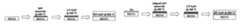
- FIGS. 1( a ) and ( b )are schematic diagrams of an exemplary method according to the invention to grow thick, substantially crack-free, Group III-Nitrides film on Si substrates using a nanostructured interlayer (a) randomly oriented, and b) well aligned nanorods.
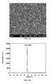
- FIG. 3shows LT-GaN deposited on top of InN nanorods on Si: a, b—SEM images; c—EDS spectrum, d—LRXRD spectrum.
- FIG. 4shows a thick (28 ⁇ m) substantially crack free GaN grown on Si using nanorod interlayer: a—plane view scanned SEM image; b—scanned XSEM, c—LRXRD spectrum; d—free-standing GaN.
- FIG. 5( a )shows a wide area scanned SEM plan-view of 30 min LT-GaN grown on InN nanorods.
- FIG. 5( b )is a scanned cross-sectional view that shows that the thickness of the LT-GaN was ⁇ 4 ⁇ m and that voids were formed at the interface.
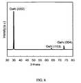
- FIG. 5( c )is an XRD ⁇ -2 ⁇ scan showing GaN (002), InN (002), and InN (101) peaks, as well as the Si (111) substrate peak.
- the low resolution XRDshows GaN (002), (004), and (103) peaks. No InN was detected.
- a layered group III-nitride articlecomprises a single crystal silicon comprising substrate and a highly textured crystal group III-nitride layer disposed on the silicon substrate.
- the highly textured group III-nitride layeris crack free and has a thickness of at least 10 ⁇ m, such as 15 to 50 ⁇ m.
- the silicon substrateis preferably (111) oriented.
- the substratecan be other orientations, such as (100).
- the structure of the nanostructured In x Ga 1-x N (1 ⁇ x ⁇ 0) interlayer usedis preferably nanorods from 300 to 700 nm in diameter. Such nanorods are nanocrystalline single crystal dislocation free having a [00.1] growth axis.
- the highly textured group III-nitride layeris selected from the group consisting of GaN, InN, AlN and their solid solutions.
- semiconductor materialssuch as II-VI and IV-VI materials, as well as carbon nanotubes, can be disposed on the nanostructured interlayer.
- the nanostructured In x Ga 1-x N (1 ⁇ x ⁇ 0)can comprise a plurality of crystalline nanorods, which can be randomly oriented or aligned with one another.
- a thickness of the nanostructured interlayeris generally from 0.1 to 3.0 ⁇ m.
- a method for forming textured group III-nitride layerscomprises the steps of providing a single crystal silicon comprising substrate, the silicon substrate preferably having a thin (native; about 15 to 20 angstrom) silicon dioxide layer disposed thereon, depositing a nanostructured In x Ga 1-x N (1 ⁇ x ⁇ 0) interlayer on the silicon substrate, and depositing a highly textured group III-nitride layer on the interlayer.
- the native oxide layer on the silicon substrateis not removed prior to depositing the nanostructured interlayer.
- the interlayer growthgenerally is performed on the Si substrate at low temperature, such as T ⁇ 600° C.
- the indium mole fractioncan be varied to obtain a desired value in the entire compositional range (0 ⁇ x ⁇ 1).
- different mole fractions of Incan be controlled by varying the ratio of the inlet flow rate of an In comprising reagent, such as trimethyl indium (TMIn) to the total group III flow rate.
- TMIntrimethyl indium
- the Ga comprising reagentis triethyl gallium (TEGa)
- TEGatriethyl gallium
- the total group III flow rateis the flow rate of TMIn plus TEGa
- the flow ratio noted aboveis (TMIn/[TMIn+TEGa]).
- the step of depositing a highly textured group III-nitride layercan comprise a first group III-nitride layer deposition at a first temperature followed by a second group III-nitride layer deposition at a second temperature, wherein the second temperature is generally 150° C. greater than the first temperature.
- Two exemplary approachesare provided for the annealing procedure:
- Free-standing III-Nitridescan also be grown using the invention by first depositing a nanostructured In x Ga 1-x N (1 ⁇ x ⁇ 0) at the interface along with a certain post grown annealing procedure.
- Free-standing as used hereinrefers to relatively thick ( ⁇ 50 ⁇ m) film that is separated from the substrate.
- the inventionis expected to provide improved provide improved group III-nitride-based devices.
- the inventioncan provide improved RF and microwave components for wireless industry, such as those based on high-electron mobility transistors (HEMTs).
- HEMTshigh-electron mobility transistors
- H-MOVPEhas several advantages. The quick switching of precursors made it possible to grow InN nanorods and GaN without taking the wafers out from the reactor. It can also ease regulation of the amount of precursors which has been found to control the diameter, length, and density of the nanorods.
- native oxide layerrefers to the silicon dioxide layer that forms on the surface of a silicon wafer from exposure to oxygen at or near room temperature.
- a thin native SiO 2 layermay help the nucleation of nanorods.
- the substratewas heated to 600° C. at a rate of 15° C./min.
- the precursors for the InN nanorod growth for the interlayerwere trimethylindium (solution TMIn, Epichem), hydrogen chloride (10% HCl, 90% N 2 , Air Products), and ammonia (grade 5 anhydrous NH 3 , Matheson-Tri gas) with N 2 carrier gas.
- the reactorwas cooled and the low temperature (LT) GaN initial layer was deposited at 560° C. for 15 to 60 minutes with an approximate LT GaN thickness of thickness of 0.1-3.0 ⁇ m min.
- the temperature of the reactorwas then increased to 850° C. after the LT-GaN growth.
- N 2was always provided.
- High temperature (HT) GaN (850° C.)was subsequently grown on top of LT-GaN and thick GaN (>20 ⁇ m) was obtained without cracking.
- the reactorwas cooled in N 2 ambient. The cooling rate was about ⁇ 15° C./min.
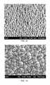
- FIGS. 2( a ) and ( b )are scanned SEM plane views of the deposited InN nanorods.
- the average diameter of InN nanorodswas around 100 nm and the length was around 1 ⁇ m. Hexagonal, well-faceted features show that individual nanorods had very good crystal quality.
- An XRD ⁇ -2 ⁇ scanshows typical InN crystal patterns with Si(111) substrate peak (see FIG. 2( c )).
- a SiO 2 layerwas observed by XRD.
- the native oxidewas intentionally not removed by etching to facilitate the nucleation of nanorods.
- the In:N ratiowas determined to be 1:0.85. Carbon and oxygen were detected and origin was due to the chemosorption. No Cl was detected using the AES technique.
- FIG. 4is a scanned SEM showing crack-free 28.4 ⁇ m thick GaN film grown on a single crystal Si(111) wafer. No cracks were observed by SEM over the entire film as seen in FIG. 4( b ). High crystalline quality of the GaN film was demonstrated using XRD ⁇ -2 ⁇ scan. The FWHM of GaN (002) peak was 341 arc sec. No Si(111) peak was detected due to screening by the thick GaN film.
- Low temperature (60° C.)-GaNwas grown on the 4 different InN interlayers/Si for comparison of the structural effects of InN.
- LT-GaNwas grown on various InN crystals for 10, 20, and 30 min.
- FIG. 5( a )shows a wide area scanned SEM plan-view of 30 min LT-GaN grown on InN nanorods.
- LT-GaNstarted to coalescence after 30 min, and an interesting embossed pattern could be seen.
- the scanned cross-sectional view( FIG. 5( b )) shows that the thickness of the LT-GaN was ⁇ 4 ⁇ m and that voids were formed at the interface.
- XRD ⁇ -2 ⁇ scanFIG. 5( c )
- This datashows that InN nanorods still exist after 30 min LT-GaN growth. This was expected since 560° C. is well below the decomposition temperature of InN. No In metal was detected by the XRD.
- Thick GaN filmswere grown at 850° C. for 2 hr after the 30 min LT-GaN growth on InN crystals described above.
- Thick GaN films having a thickness of about 20 ⁇ mwere deposited.
- Thick GaN grown on the InN columnar film/Sishowed significant peeling of the GaN film, but no cracks.
- Thick GaN film on InN microrods on Sishowed cracks.
- the GaN filmoccasionally self-separated from the Si substrates without effort.
- Low resolution XRD shown in FIG. 6shows GaN (002), (004), and (103) peaks. No InN was detected presumably because at the growth temperature (850° C.), the InN dissolved into the In x Ga 1-x N.
- the filmwas polycrystalline, but highly textured along the [002] axis with an FWHM of 341 arcsec.
Landscapes
- Engineering & Computer Science (AREA)
- Physics & Mathematics (AREA)
- Condensed Matter Physics & Semiconductors (AREA)
- General Physics & Mathematics (AREA)
- Manufacturing & Machinery (AREA)
- Computer Hardware Design (AREA)
- Microelectronics & Electronic Packaging (AREA)
- Power Engineering (AREA)
- Chemical & Material Sciences (AREA)
- Crystallography & Structural Chemistry (AREA)
- Materials Engineering (AREA)
- Crystals, And After-Treatments Of Crystals (AREA)
Abstract
Description
This application is a divisional application of U.S. application Ser. No. 11/512,615, filed Aug. 29, 2006, which claims the priority benefit of U.S. Provisional Application No. 60/712,922, filed on Aug. 31, 2005, both of which are incorporated herein by reference.
The United States Government has certain rights in this invention pursuant to a grant from the U.S. Air Force grant number FA8650-04-2-1619.
GaN and related materials continue to grow in importance for optical and electronic devices. As in other semiconductor systems, epitaxial growth of GaN ideally occurs on GaN substrates cut from bulk GaN single crystals. Bulk crystal growth of GaN, however, requires extremely high pressure to maintain the nitrogen content in the crystal, rendering bulk growth extremely difficult. For this reason, the high volume production of large size, bulk GaN is improbable in the near future and the search for alternative substrates continues.
Two of the main factors associated with substrate choice are cost and resulting GaN epilayer quality. Silicon is increasingly being used as a substrate for GaN deposition because Si substrates are available at comparatively low cost, high quality, large area, and large quantity, thus presenting many manufacturing advantages over other available substrates for GaN, such as sapphire and SiC.
The disadvantages of Si as a substrate for GaN heteroepitaxy include an a-plane+20.5% misfit which led to the conclusion that growth of GaN directly on silicon was unfeasible. Moreover, the thermal expansion misfit between GaN (5.6×10⁻⁶K−1) and Si (6.2×10⁻⁶K−1) of 9.6% can lead to cracking upon cooling in films grown at high temperature, and, at elevated temperature, melt-back etching between Ga and the Si substrate during the initial stages of growth or at stress is known to induce cracks that form in GaN films during GaN deposition.
Traditionally these issues trigger polycrystalline GaN growth on Si substrates. Typically, thin AlN buffer layers are used to absorb the lattice mismatch between the GaN film and the Si substrate. The subsequent deposition of GaN introduces significant strain into the structure due the large lattice mismatch along with the resultant high density of defects that introduce additional tensile stress into the film. This tensile stress is exacerbated during cool down from growth temperature with macro-crack formation customary for GaN films thicker than 1 μm.
To overcome GaN cracking problems, different techniques have been used including use of multiple AlN interlayers, AlGaN graded layers, patterned Si, and in situ SiN masking (non-uniform deposition). These methods were reported to provide some decrease in bowing and cracking, but no method successfully produced crack-free thick (e.g. >10 μm) GaN films likely because there still remains excessive tensile stress, as well as strong cohesion between GaN (or AlN buffer layer) and Si. Although ˜7 μm thick crack-free GaN on Si has been reported by incorporating multiple AlN interlayers, the maximum thickness of a commercially available crack-free GaN layer on Si is about 1 μm.
Cracks can be generated during growth or cooling due to the excess tensile stress caused by large lattice and thermal expansion differences. It has been observed by the present Inventors that the cracks penetrate through the Si substrate and separation occurs inside the Si substrate. The strong cohesion between GaN and Si (or AlN and Si in GaN/AlGaN/AlN/Si template case), as well as the brittleness of Si, are responsible for cracking to take place in pre interior of the Si wafer. The bond strength of Si—Si is 7 eV which is lower than and the Ga—N (8.9 eV) or Al—N (11.5 eV) and Si—N (10.5 eV). The bond strength of Si—Si is the weakest. The nano-indentation hardnesses of the GaN, AlN, and Si are 20, 18 and 14 GPa, respectively. Therefore, the cracking penetration to the Si substrate observed by the present Inventors was expected. This brittleness of Si added with the large tensile stress created by the lattice mismatch and thermal expansion differences makes the growth of crack-free GaN on Si even more challenging.
A layered group III-nitride article comprises a single crystal silicon comprising substrate and a highly textured crystal group III-nitride layer disposed on the silicon substrate. The highly textured group III-nitride layer is crack free and has a thickness of at least 10 μm, such as 15 to 50 μm. As used herein, the term “highly textured” as applied to the group III-nitride layer refers to a layer which provides (i) a full width half maximum (FWHM) X-ray ω-scan rocking curve of no more than 20 arc-min, more preferably less than 10 arc-min, and most preferably less than 7 arc-min, and (ii) an XRD pole figure (Phi scan) that provides a highly non-uniform pole density that is clustered around the number of points characteristic of the particular orientation. For example, regarding the XRD, highly textured GaN will evidence only 2 peaks being at (002) and (004) in a LRXRD spectrum. Crack free is defined herein refers to an area of at least 25 mm2being “crack-free” as confirmed by SEM, AFM, or TEM.
The silicon substrate can be (111), (100) or other orientations. In a preferred embodiment, the highly textured group III-nitride layer comprises GaN. In this preferred embodiment, the article can further comprise a thin layer of a In—Ga—N alloy at an interface between the GaN layer and the silicon substrate.
A method for forming highly textured group III-nitride layers comprises the steps of providing a single crystal silicon comprising substrate, depositing a nanostructured InxGa1-xN (1≧x≧0) interlayer on the silicon substrate, and depositing a highly textured group III-nitride layer on the interlayer. The interlayer has a nano indentation hardness that is less than both the silicon substrate and the highly textured group III-nitride layer. The group III-nitride layer can be GaN and the interlayer can be InN. The step of depositing a highly textured group III-nitride layer preferably comprises a first group III-nitride layer deposition at a first temperature followed by a second group III-nitride layer deposition at a second temperature, wherein the first temperature is below a decomposition temperature of the InxGa1-xN (1≧x≧0) and the second temperature is at least 150° C. greater than the first temperature.
The highly textured group III-nitride layer is generally crack free and has a thickness of at least 10 μm. The nanostructured InxGa1-xN (1≧x≧0) interlayer can comprise a columnar film or nanorods having an average rod diameter of 300 to 700 nm. The silicon substrate is preferably (111) oriented.
It has been found by the inventors that a suitably nanostructured InxGa1-xN (1≧x≧0) interlayer relieves much of the stress at the Si substrate-group III-nitride film interface during group III-nitride film deposition and thus prevents crack formation during growth of thick (≧1 μm) group III-nitride films thereon. A layered group III-nitride article comprises a single crystal silicon comprising substrate and a highly textured crystal group III-nitride layer disposed on the silicon substrate. The highly textured group III-nitride layer is crack free and has a thickness of at least 10 μm, such as 15 to 50 μm.
The silicon substrate is preferably (111) oriented. However, the substrate can be other orientations, such as (100).
The structure of the nanostructured InxGa1-xN (1≧x≧0) interlayer used is preferably nanorods from 300 to 700 nm in diameter. Such nanorods are nanocrystalline single crystal dislocation free having a [00.1] growth axis.
In a preferred embodiment, the highly textured group III-nitride layer is selected from the group consisting of GaN, InN, AlN and their solid solutions. However, more generally, and other semiconductor materials, such as II-VI and IV-VI materials, as well as carbon nanotubes, can be disposed on the nanostructured interlayer.
The nanostructured InxGa1-xN (1≧x≧0) can comprise a plurality of crystalline nanorods, which can be randomly oriented or aligned with one another. A thickness of the nanostructured interlayer is generally from 0.1 to 3.0 μm.
A method for forming textured group III-nitride layers comprises the steps of providing a single crystal silicon comprising substrate, the silicon substrate preferably having a thin (native; about 15 to 20 angstrom) silicon dioxide layer disposed thereon, depositing a nanostructured InxGa1-xN (1≧x≧0) interlayer on the silicon substrate, and depositing a highly textured group III-nitride layer on the interlayer. Thus, in a preferred embodiment, the native oxide layer on the silicon substrate is not removed prior to depositing the nanostructured interlayer.
The interlayer growth generally is performed on the Si substrate at low temperature, such as T<600° C. The indium mole fraction can be varied to obtain a desired value in the entire compositional range (0≦x≦1). In practice, different mole fractions of In can be controlled by varying the ratio of the inlet flow rate of an In comprising reagent, such as trimethyl indium (TMIn) to the total group III flow rate. When the Ga comprising reagent is triethyl gallium (TEGa), the total group III flow rate is the flow rate of TMIn plus TEGa, and the flow ratio noted above is (TMIn/[TMIn+TEGa]).
The step of depositing a highly textured group III-nitride layer can comprise a first group III-nitride layer deposition at a first temperature followed by a second group III-nitride layer deposition at a second temperature, wherein the second temperature is generally 150° C. greater than the first temperature. Two exemplary approaches are provided for the annealing procedure:
- I: in situ slowly cooling down after the growth when reactor is off from the growth to room temperature, and
- II: after growth annealing in N2or NH3at the growth temperature (T=850 C, 15 to 30 min).
Free-standing III-Nitrides can also be grown using the invention by first depositing a nanostructured InxGa1-xN (1≧x≧0) at the interface along with a certain post grown annealing procedure. Free-standing as used herein refers to relatively thick (≧50 μm) film that is separated from the substrate.
The invention is expected to provide improved provide improved group III-nitride-based devices. For example, the invention can provide improved RF and microwave components for wireless industry, such as those based on high-electron mobility transistors (HEMTs).
It should be understood that the Examples described below are provided for illustrative purposes only and do not in any way define the scope of the invention.
In the Examples described below, two types of reactors were used to deposit GaN. The primary reactor used was a quartz hot-wall merged-hydride reactor that can alternate between MOCVD and HVPE. H-MOVPE has several advantages. The quick switching of precursors made it possible to grow InN nanorods and GaN without taking the wafers out from the reactor. It can also ease regulation of the amount of precursors which has been found to control the diameter, length, and density of the nanorods.
Si(111) substrates were cleaned by trichloroethylene, acetone, and methanol followed by DI water rinse and N2dry. Etching was purposely not carried out to take advantage of native oxide layer for nanorod growth. As used herein, the phrase “native oxide layer” refers to the silicon dioxide layer that forms on the surface of a silicon wafer from exposure to oxygen at or near room temperature.
It was believed that a thin native SiO2layer may help the nucleation of nanorods. After loading, the substrate was heated to 600° C. at a rate of 15° C./min. The precursors for the InN nanorod growth for the interlayer were trimethylindium (solution TMIn, Epichem), hydrogen chloride (10% HCl, 90% N2, Air Products), and ammonia (grade 5 anhydrous NH3, Matheson-Tri gas) with N2carrier gas. Reactor pressure P=760 Torr, T=600° C., NH3/TMIn=250, HCl/TMIn=4. Flow rates: TMIn=0.7 sccm; HN3=175 sccm, HCl (10%)=28 sccm, N2=1600 sccm.
After growth of the InN nanorods, the reactor was cooled and the low temperature (LT) GaN initial layer was deposited at 560° C. for 15 to 60 minutes with an approximate LT GaN thickness of thickness of 0.1-3.0 μm min. The temperature of the reactor was then increased to 850° C. after the LT-GaN growth. During the heating and cooling processes N2was always provided. High temperature (HT) GaN (850° C.) was subsequently grown on top of LT-GaN and thick GaN (>20 μm) was obtained without cracking. After growth, the reactor was cooled in N2ambient. The cooling rate was about −15° C./min.
Experiments regarding InN nanostructured buffer growth on Si is now described. InN columnar film, small nanorods (d=250 nm), large nanorods (d=500 nm), and microrods were grown on Si substrates at different conditions listed in the Table below and used as templates for thick GaN growth.
| Growth conditions for InN buffer interlayer on Si. |
| Growth T (° C.) | Cl/In | N/In | Time | Feature |
| 560 | 1 | 2500 | 1 | hr | (a) |
| 600 | 4 | 250 | 20 | min | (b) Nanorods (d = 250 nm) |
| 600 | 4 | 250 | 1 | hr | (c) Nanorods (d = 500 nm) |
| 650 | 5 | 250 | 1 | hr | (d) Microrods |
Experiments regarding low-temperature GaN growth on InN nano/Si templates are now described. Low temperature (560° C.)-GaN was grown on the 4 different InN interlayers/Si for comparison of the structural effects of InN. LT-GaN was grown on various InN crystals for 10, 20, and 30 min. The growth conditions for LT-GaN were set as T=560° C., Cl/In=1.5, and N/In=570. It was observed that only InN columnar films and larger nanorods (d=500 nm) provided uniform coverage of LT-GaN, while the smaller nanorods (d=250 nm) and microrods demonstrated non-uniform coverage of LT-GaN. It was found that GaN deposition occurred mainly on the InN surface, rather than on the Si substrate.
High-temperature GaN growth on LT-GaN/InN/Si(111) then followed. Thick GaN films were grown at 850° C. for 2 hr after the 30 min LT-GaN growth on InN crystals described above. The growth conditions for HT-GaN were as follows: Cl/Ga=1.5, N/Ga=570, and T=850° C. N2was used as the carrier gas. Thick GaN films having a thickness of about 20 μm were deposited. Thick (about 20 μm) GaN films were grown on LT-GaN for each of an InN columnar film, small InN nanorods (d=250 nm), large InN nanorods (d=500 nm), and InN microrods. Thick GaN grown on the InN columnar film/Si showed significant peeling of the GaN film, but no cracks. Thick GaN grown on smaller InN nanorods (d=250 nm) over Si(111) showed cracks likely due to the non-uniform deposition of InN nanorods and LT-GaN. Thick GaN film on InN microrods on Si showed cracks.
The best result for crack-free thick GaN was found for growth on the large InN nanorod (d=500 nm) interlayer. Although the surface was found to be is still rough, the data obtained makes it clear that dense and uniform InN nanorods can provide a good structure for thick, crack-free GaN growth on Si(111).
The GaN film occasionally self-separated from the Si substrates without effort. SEM and XRD were obtained for freestanding and crack-free GaN film (28 μm thick) grown on InN nanorods (d=500 nm)/Si (111) substrates. No cracks were observed by SEM over the wide range of the film. Low resolution XRD shown inFIG. 6 shows GaN (002), (004), and (103) peaks. No InN was detected presumably because at the growth temperature (850° C.), the InN dissolved into the InxGa1-xN. The film was polycrystalline, but highly textured along the [002] axis with an FWHM of 341 arcsec.
A cross-sectional SEM view of crack-free thick (40 μm) GaN grown on Si substrate using dense and large (d=500 nm) InN nanorods was obtained. In this case, self-separation did not occur. InN nanorods at the interface were not visible after HT-GaN. InN likely dissolved into GaN to form InxGa1-xN alloy at the interface.
This invention can be embodied in other forms without departing from the spirit or essential attributes thereof and, accordingly, reference should be had to the following claims rather than the foregoing specification as indicating the scope of the invention.
Claims (15)
1. A method for forming highly textured group III-nitride layers, comprising the steps of:
providing a single crystal silicon comprising substrate;
depositing a nanostructured InxGa1-xN (1≧x≧0) interlayer on said silicon substrate, the nanostructured InxGa1-xN interlayer being directly disposed on the silicon substrate and being in contact with said silicon substrate; a surface of the substrate that contacts the nanostructured interlayer being flat; and
depositing a highly textured group III-nitride layer on said interlayer, wherein said interlayer has a nano indentation hardness that is less than both said silicon substrate and said highly textured group III-nitride layer; wherein said interlayer comprises a columnar film or nanorods having average rod diameters of 300 to 700 nm.
2. The method ofclaim 1 , wherein said step of depositing a highly textured group III-nitride layer comprises a first group III-nitride layer deposition at a first temperature followed by a second group III-nitride layer deposition at a second temperature, wherein said first temperature is below a decomposition temperature of said InxGa1-xN and said second temperature is at least 150° C. greater than said first temperature.
3. The method ofclaim 1 , wherein said highly textured group III nitride layer is crack free and has a thickness of at least 10 μm.
4. The method ofclaim 1 , wherein said silicon substrate is (111) oriented.
5. The method ofclaim 1 , wherein said highly textured group III-nitride layer comprises GaN.
6. The method ofclaim 1 , wherein x=1, said interlayer being InN.
7. The method ofclaim 1 , wherein said interlayer comprises randomly oriented nanorods.
8. The method ofclaim 1 , wherein said interlayer comprises a plurality of nanorods aligned with one another.
9. A method for forming highly textured group III-nitride layers, comprising the steps of:
providing a single crystal silicon comprising substrate;
depositing a nanostructured InxGa1-xN (1≧x≧0) interlayer on said silicon substrate, the nanostructured InxGa1-xN interlayer being directly disposed on the silicon substrate and being in contact with said silicon substrate; a surface of the substrate that contacts the nanostructured interlayer being smooth; and
depositing a highly textured group III-nitride layer on said interlayer, wherein said interlayer has a nano indentation hardness that is less than both said silicon substrate and said highly textured group III-nitride layer; wherein said interlayer comprises a columnar film or nanorods.
10. The method ofclaim 9 , wherein said step of depositing a highly textured group III-nitride layer comprises a first group III-nitride layer deposition at a first temperature followed by a second group III-nitride layer deposition at a second temperature, wherein said first temperature is below a decomposition temperature of said InxGa1-xN and said second temperature is at least 150° C. greater than said first temperature.
11. The method ofclaim 9 , wherein said highly textured group III nitride layer is crack free and has a thickness of at least 10 μm.
12. The method ofclaim 9 , wherein said highly textured group III-nitride layer comprises GaN.
13. The method ofclaim 9 , wherein x=1, said interlayer being InN.
14. The method ofclaim 9 , wherein said interlayer comprises randomly oriented nanorods.
15. The method ofclaim 9 , wherein said interlayer comprises a plurality of nanorods aligned with one another.
Priority Applications (2)
| Application Number | Priority Date | Filing Date | Title |
|---|---|---|---|
| US12/257,567US8268646B2 (en) | 2005-08-31 | 2008-10-24 | Group III-nitrides on SI substrates using a nanostructured interlayer |
| US12/861,614US8222057B2 (en) | 2006-08-29 | 2010-08-23 | Crack free multilayered devices, methods of manufacture thereof and articles comprising the same |
Applications Claiming Priority (3)
| Application Number | Priority Date | Filing Date | Title |
|---|---|---|---|
| US71292205P | 2005-08-31 | 2005-08-31 | |
| US11/512,615US8946674B2 (en) | 2005-08-31 | 2006-08-29 | Group III-nitrides on Si substrates using a nanostructured interlayer |
| US12/257,567US8268646B2 (en) | 2005-08-31 | 2008-10-24 | Group III-nitrides on SI substrates using a nanostructured interlayer |
Related Parent Applications (2)
| Application Number | Title | Priority Date | Filing Date |
|---|---|---|---|
| US11/512,615DivisionUS8946674B2 (en) | 2005-08-31 | 2006-08-29 | Group III-nitrides on Si substrates using a nanostructured interlayer |
| US11/512,615Continuation-In-PartUS8946674B2 (en) | 2005-08-31 | 2006-08-29 | Group III-nitrides on Si substrates using a nanostructured interlayer |
Related Child Applications (2)
| Application Number | Title | Priority Date | Filing Date |
|---|---|---|---|
| US11/512,615Continuation-In-PartUS8946674B2 (en) | 2005-08-31 | 2006-08-29 | Group III-nitrides on Si substrates using a nanostructured interlayer |
| US12/861,614Continuation-In-PartUS8222057B2 (en) | 2006-08-29 | 2010-08-23 | Crack free multilayered devices, methods of manufacture thereof and articles comprising the same |
Publications (2)
| Publication Number | Publication Date |
|---|---|
| US20100029064A1 US20100029064A1 (en) | 2010-02-04 |
| US8268646B2true US8268646B2 (en) | 2012-09-18 |
Family
ID=38039831
Family Applications (2)
| Application Number | Title | Priority Date | Filing Date |
|---|---|---|---|
| US11/512,615Expired - Fee RelatedUS8946674B2 (en) | 2005-08-31 | 2006-08-29 | Group III-nitrides on Si substrates using a nanostructured interlayer |
| US12/257,567Expired - Fee RelatedUS8268646B2 (en) | 2005-08-31 | 2008-10-24 | Group III-nitrides on SI substrates using a nanostructured interlayer |
Family Applications Before (1)
| Application Number | Title | Priority Date | Filing Date |
|---|---|---|---|
| US11/512,615Expired - Fee RelatedUS8946674B2 (en) | 2005-08-31 | 2006-08-29 | Group III-nitrides on Si substrates using a nanostructured interlayer |
Country Status (1)
| Country | Link |
|---|---|
| US (2) | US8946674B2 (en) |
Cited By (5)
| Publication number | Priority date | Publication date | Assignee | Title |
|---|---|---|---|---|
| US20130104802A1 (en)* | 2006-11-22 | 2013-05-02 | Soitec | Gallium trichloride injection scheme |
| US9481944B2 (en) | 2006-11-22 | 2016-11-01 | Soitec | Gas injectors including a funnel- or wedge-shaped channel for chemical vapor deposition (CVD) systems and CVD systems with the same |
| US9601340B2 (en) | 2014-04-11 | 2017-03-21 | Samsung Electronics Co., Ltd. | Electronic device having quantum dots and method of manufacturing the same |
| US9917156B1 (en) | 2016-09-02 | 2018-03-13 | IQE, plc | Nucleation layer for growth of III-nitride structures |
| US12125938B2 (en)* | 2006-02-23 | 2024-10-22 | Azur Space Solar Power Gmbh | Nitride semiconductor component and process for its production |
Families Citing this family (15)
| Publication number | Priority date | Publication date | Assignee | Title |
|---|---|---|---|---|
| TW200806829A (en)* | 2006-07-20 | 2008-02-01 | Univ Nat Central | Method for producing single crystal gallium nitride substrate |
| DE102007029576A1 (en)* | 2007-06-26 | 2009-01-08 | Evonik Degussa Gmbh | Process for the production of film-like semiconductor materials and / or electronic elements by prototyping and / or coating |
| TWI384548B (en)* | 2008-11-10 | 2013-02-01 | Univ Nat Central | Method for producing nitride crystal film, nitride film and substrate structure |
| US8338226B2 (en)* | 2009-04-02 | 2012-12-25 | Semiconductor Energy Laboratory Co., Ltd. | Method for manufacturing semiconductor device |
| US8138069B2 (en)* | 2009-04-24 | 2012-03-20 | Applied Materials, Inc. | Substrate pretreatment for subsequent high temperature group III depositions |
| US8110889B2 (en)* | 2009-04-28 | 2012-02-07 | Applied Materials, Inc. | MOCVD single chamber split process for LED manufacturing |
| US8575660B2 (en)* | 2009-10-14 | 2013-11-05 | International Rectifier Corporation | Group III-V semiconductor device with strain-relieving interlayers |
| KR20180006507A (en)* | 2010-02-05 | 2018-01-17 | 가부시키가이샤 한도오따이 에네루기 켄큐쇼 | Semiconductor device and method for manufacturing the same |
| US8980730B1 (en)* | 2010-09-14 | 2015-03-17 | Stc.Unm | Selective nanoscale growth of lattice mismatched materials |
| JP2013542599A (en)* | 2010-09-30 | 2013-11-21 | フリースケール セミコンダクター インコーポレイテッド | Method for processing a semiconductor wafer, semiconductor wafer and semiconductor device |
| KR20130081956A (en)* | 2012-01-10 | 2013-07-18 | 삼성전자주식회사 | Method for growing nitride semiconductor |
| US9236271B2 (en)* | 2012-04-18 | 2016-01-12 | Globalfoundries Inc. | Laser-initiated exfoliation of group III-nitride films and applications for layer transfer and patterning |
| FR2997551B1 (en)* | 2012-10-26 | 2015-12-25 | Commissariat Energie Atomique | METHOD OF MANUFACTURING SEMICONDUCTOR STRUCTURE AND SEMICONDUCTOR COMPONENT COMPRISING SUCH A STRUCTURE |
| CN107429383B (en)* | 2015-03-30 | 2020-07-24 | 东曹株式会社 | Gallium nitride based sintered body and method for producing the same |
| CN109755369A (en)* | 2019-01-04 | 2019-05-14 | 浙江大学 | Silicon-based III-V semiconductor heteronano-pillar electroluminescent device and preparation method |
Citations (77)
| Publication number | Priority date | Publication date | Assignee | Title |
|---|---|---|---|---|
| US5310596A (en) | 1990-08-10 | 1994-05-10 | Norton Company | Multi-layer superhard film structure |
| WO1999014797A1 (en) | 1997-09-15 | 1999-03-25 | Cornell Research Foundation, Inc. | Compliant universal substrates for epitaxial growth |
| WO1999019546A1 (en) | 1997-10-10 | 1999-04-22 | Cornell Research Foundation, Inc. | Methods for growing defect-free heteroepitaxial layers |
| JPH11186178A (en) | 1997-12-22 | 1999-07-09 | Toyoda Gosei Co Ltd | Gallium nitride-based compound semiconductor and its manufacture |
| US6022622A (en) | 1996-09-06 | 2000-02-08 | Sanyo Electric Co., Ltd. | Hard carbon film-coated substrate and method for fabricating the same |
| US6086673A (en) | 1998-04-02 | 2000-07-11 | Massachusetts Institute Of Technology | Process for producing high-quality III-V nitride substrates |
| US6238980B1 (en) | 1998-07-07 | 2001-05-29 | Fuji Electric Co., Ltd. | Method for manufacturing silicon carbide MOS semiconductor device including utilizing difference in mask edges in implanting |
| US20010023942A1 (en) | 2000-03-23 | 2001-09-27 | Samsung Electronics Co., Ltd. | Semiconductor device of heterojunction structure having quantum dot buffer layer |
| US6339257B1 (en) | 1999-01-28 | 2002-01-15 | Mitsubishi Denki Kabushiki Kaisha | Semiconductor device |
| US20020013042A1 (en) | 2000-04-17 | 2002-01-31 | Hadis Morkoc | Defect reduction in GaN and related materials |
| US20020017650A1 (en) | 1997-11-18 | 2002-02-14 | Technologies & Devices | III-V compound semiconductor device with an InGaN1-x-yPxASy non-continuous quantum dot layer |
| US6376339B2 (en) | 1998-11-24 | 2002-04-23 | North Carolina State University | Pendeoepitaxial methods of fabricating gallium nitride semiconductor layers on silicon carbide substrates by lateral growth from sidewalls of masked posts, and gallium nitride semiconductor structures fabricated thereby |
| US20020047135A1 (en) | 1997-11-18 | 2002-04-25 | Nikolaev Audrey E. | P-N junction-based structures utilizing HVPE grown III-V compound layers |
| WO2002045140A2 (en) | 2000-11-22 | 2002-06-06 | Motorola, Inc. | Semiconductor structures having a compliant substrate |
| JP2002164521A (en) | 2000-11-28 | 2002-06-07 | Sharp Corp | Semiconductor substrate and manufacturing method thereof |
| US6406540B1 (en) | 1999-04-27 | 2002-06-18 | The United States Of America As Represented By The Secretary Of The Air Force | Process and apparatus for the growth of nitride materials |
| US6423983B1 (en) | 2000-10-13 | 2002-07-23 | North Carolina State University | Optoelectronic and microelectronic devices including cubic ZnMgO and/or CdMgO alloys |
| US6447604B1 (en) | 2000-03-13 | 2002-09-10 | Advanced Technology Materials, Inc. | Method for achieving improved epitaxy quality (surface texture and defect density) on free-standing (aluminum, indium, gallium) nitride ((al,in,ga)n) substrates for opto-electronic and electronic devices |
| US20020136932A1 (en) | 2001-03-21 | 2002-09-26 | Seikoh Yoshida | GaN-based light emitting device |
| EP1246233A2 (en) | 2001-03-27 | 2002-10-02 | Nec Corporation | Semiconductor substrate made of group III nitride, and process for manufacture thereof |
| US6472300B2 (en) | 1997-11-18 | 2002-10-29 | Technologies And Devices International, Inc. | Method for growing p-n homojunction-based structures utilizing HVPE techniques |
| US6476420B2 (en) | 1997-11-18 | 2002-11-05 | Technologies And Devices International, Inc. | P-N homojunction-based structures utilizing HVPE growth III-V compound layers |
| US6479839B2 (en) | 1997-11-18 | 2002-11-12 | Technologies & Devices International, Inc. | III-V compounds semiconductor device with an AlxByInzGa1-x-y-zN non continuous quantum dot layer |
| JP2003022973A (en) | 2001-07-06 | 2003-01-24 | Sanyo Electric Co Ltd | Nitride system semiconductor device and method of forming it |
| US6555452B2 (en) | 1997-11-18 | 2003-04-29 | Technologies And Devices International, Inc. | Method for growing p-type III-V compound material utilizing HVPE techniques |
| US6559038B2 (en) | 1997-11-18 | 2003-05-06 | Technologies And Devices International, Inc. | Method for growing p-n heterojunction-based structures utilizing HVPE techniques |
| US6559467B2 (en) | 1997-11-18 | 2003-05-06 | Technologies And Devices International, Inc. | P-n heterojunction-based structures utilizing HVPE grown III-V compound layers |
| US6596377B1 (en) | 2000-03-27 | 2003-07-22 | Science & Technology Corporation @ Unm | Thin film product and method of forming |
| US6599133B2 (en) | 1997-11-18 | 2003-07-29 | Technologies And Devices International, Inc. | Method for growing III-V compound semiconductor structures with an integral non-continuous quantum dot layer utilizing HVPE techniques |
| US20030155574A1 (en) | 2002-02-15 | 2003-08-21 | Doolittle William Alan | Semiconductor devices formed of III-nitride compounds, lithium-niobate-tantalate, and silicon carbide |
| US6610144B2 (en) | 2000-07-21 | 2003-08-26 | The Regents Of The University Of California | Method to reduce the dislocation density in group III-nitride films |
| JP2003243316A (en) | 2002-02-20 | 2003-08-29 | Fuji Photo Film Co Ltd | Substrate for semiconductor element and its manufacturing method |
| US6617060B2 (en)* | 2000-12-14 | 2003-09-09 | Nitronex Corporation | Gallium nitride materials and methods |
| US6630690B2 (en) | 1997-10-07 | 2003-10-07 | Cree, Inc. | Group III nitride photonic devices on silicon carbide substrates with conductive buffer interlayer structure |
| US6649942B2 (en) | 2001-05-23 | 2003-11-18 | Sanyo Electric Co., Ltd. | Nitride-based semiconductor light-emitting device |
| US20030213964A1 (en) | 2000-03-13 | 2003-11-20 | Flynn Jeffrey S. | III-V Nitride homoepitaxial material of improved MOVPE epitaxial quality (surface texture and defect density) formed on free-standing (Al,In,Ga)N substrates, and opto-electronic and electronic devices comprising same |
| US20030232455A1 (en)* | 2002-02-28 | 2003-12-18 | Rohm Co., Ltd. | Semiconductor light emitting element and method of making the same |
| US6692568B2 (en) | 2000-11-30 | 2004-02-17 | Kyma Technologies, Inc. | Method and apparatus for producing MIIIN columns and MIIIN materials grown thereon |
| US20040061119A1 (en) | 2002-09-18 | 2004-04-01 | Sanyo Electric Co., Ltd. | Nitride-based semiconductor light-emitting device |
| US6720196B2 (en) | 2001-05-11 | 2004-04-13 | Sanyo Electric Co., Ltd. | Nitride-based semiconductor element and method of forming nitride-based semiconductor |
| US20040077156A1 (en) | 2002-10-18 | 2004-04-22 | Loucas Tsakalakos | Methods of defect reduction in wide bandgap thin films using nanolithography |
| EP1422748A1 (en) | 2001-08-01 | 2004-05-26 | Nagoya Industrial Science Research Institute | Group iii nitride semiconductor film and its production method |
| WO2004057663A1 (en) | 2002-12-19 | 2004-07-08 | Koninklijke Philips Electronics N.V. | Stress-free composite substrate and method of manufacturing such a composite substrate |
| US20040137732A1 (en) | 2000-07-07 | 2004-07-15 | Eric Frayssinet | Process for producing an epitaxial layer of gallium nitride |
| US6773946B2 (en) | 2002-11-15 | 2004-08-10 | Kwagju Institute Of Science And Technology | Method for fabricating light-emitting diode using nanosize nitride semiconductor multiple quantum wells |
| JP2004289095A (en) | 2003-03-19 | 2004-10-14 | Toshiaki Sakaida | Manufacturing method of nitride compound semiconductor |
| US6812518B2 (en) | 2001-11-01 | 2004-11-02 | Innotech Corporation | Semiconductor memory having storage cells storing multiple bits and a method of manufacturing the same |
| US6818061B2 (en) | 2003-04-10 | 2004-11-16 | Honeywell International, Inc. | Method for growing single crystal GaN on silicon |
| JP2005001961A (en) | 2003-06-13 | 2005-01-06 | Rohm Co Ltd | Group iii nitride compound semiconductor substrate |
| US6844569B1 (en) | 2003-12-20 | 2005-01-18 | Samsung Electro-Mechanics Co., Ltd. | Fabrication method of nitride-based semiconductors and nitride-based semiconductor fabricated thereby |
| US6849862B2 (en) | 1997-11-18 | 2005-02-01 | Technologies And Devices International, Inc. | III-V compound semiconductor device with an AlxByInzGa1-x-y-zN1-a-bPaAsb non-continuous quantum dot layer |
| US20050051766A1 (en) | 2003-09-05 | 2005-03-10 | The University Of North Carolina | Quantum dot optoelectronic devices with nanoscale epitaxial lateral overgrowth and methods of manufacture |
| US20050067935A1 (en) | 2003-09-25 | 2005-03-31 | Lee Ji Ung | Self-aligned gated rod field emission device and associated method of fabrication |
| US20050142391A1 (en) | 2001-07-06 | 2005-06-30 | Technologies And Devices International, Inc. | Method and apparatus for fabricating crack-free Group III nitride semiconductor materials |
| JP2005183917A (en) | 2003-12-19 | 2005-07-07 | Hynix Semiconductor Inc | Semiconductor device having pad structure capable of preventing and buffering stress of silicon nitride film |
| US20050164419A1 (en) | 2004-01-23 | 2005-07-28 | Sumitomo Electric Industries, Ltd. | Group III Nitride Crystal Substrate, Method of Its Manufacture, and Group-III Nitride Semiconductor Device |
| US20050179052A1 (en) | 2004-02-12 | 2005-08-18 | Yi Gyu C. | Heterojunction structure of nitride semiconductor and nano-device or an array thereof comprising same |
| US20050194598A1 (en)* | 2004-02-13 | 2005-09-08 | Hwa-Mok Kim | Super bright light emitting diode of nanorod array structure having InGaN quantum well and method for manufacturing the same |
| US20050199886A1 (en) | 2004-03-10 | 2005-09-15 | Siltron Inc. | Nitride semiconductor device and method of manufacturing the same |
| WO2005094271A2 (en) | 2004-03-25 | 2005-10-13 | The Regents Of The University Of California | Colloidal quantum dot light emitting diodes |
| US6958254B2 (en) | 2001-05-08 | 2005-10-25 | Btg International Limited | Method to produce germanium layers |
| US6967346B2 (en) | 2003-08-02 | 2005-11-22 | Formosa Epitaxy Incorporation | Light emitting diode structure and manufacture method thereof |
| US20060006500A1 (en) | 2004-07-07 | 2006-01-12 | Nitronex Corporation | III-nitride materials including low dislocation densities and methods associated with the same |
| US20060091408A1 (en) | 2004-10-29 | 2006-05-04 | Samsung Electro-Mechanics Co., Ltd. | Nitride based semiconductor device using nanorods and process for preparing the same |
| WO2007001099A1 (en) | 2005-06-27 | 2007-01-04 | Seoul Opto Device Co., Ltd. | Light emitting diode of a nanorod array structure having a nitride-based multi quantum well |
| WO2007001098A1 (en) | 2005-06-25 | 2007-01-04 | Seoul Opto Device Co., Ltd. | Nanostructure having a nitride-based quantum well and light emitting diode employing the same |
| WO2007007954A1 (en) | 2005-07-11 | 2007-01-18 | Seoul Opto Device Co., Ltd. | Light emitting device employing nanowire phosphors |
| WO2007021047A1 (en) | 2005-08-19 | 2007-02-22 | Postech Foundation | Light--emitting device comprising conductive nanorods as transparent electrodes |
| WO2007021069A1 (en) | 2005-08-19 | 2007-02-22 | Seoul Opto Device Co., Ltd. | Light emitting diode employing an array of nanorods and method of fabricating the same |
| WO2007021017A1 (en) | 2005-08-17 | 2007-02-22 | Ngk Insulators, Ltd. | Semiconductor layered structure and its method of formation, and light emitting device |
| WO2007032802A2 (en) | 2005-06-29 | 2007-03-22 | University Of Houston | Nanorod arrays formed by ion beam implantation |
| WO2008002104A1 (en) | 2006-06-30 | 2008-01-03 | Seoul Opto Device Co., Ltd. | Method of forming p-type compound semiconductor layer |
| US7339205B2 (en) | 2004-06-28 | 2008-03-04 | Nitronex Corporation | Gallium nitride materials and methods associated with the same |
| US20080280426A1 (en) | 2007-05-09 | 2008-11-13 | Sharp Laboratories Of America, Inc. | Gallium nitride-on-silicon interface |
| US20080283821A1 (en) | 2007-05-17 | 2008-11-20 | Samsung Corning Co., Ltd. | Method of growing gan crystal on silicon substrate, and light emitting device and method of manufacturing thereof |
| US20090243043A1 (en) | 2006-03-23 | 2009-10-01 | Wang Nang Wang | Growth method using nanostructure compliant layers and hvpe for producing high quality compound semiconductor materials |
| US20110042683A1 (en)* | 2006-08-29 | 2011-02-24 | University Of Florida Research Foundation, Inc. | Crack free multilayered devices, methods of manufacture thereof and articles comprising the same |
Family Cites Families (2)
| Publication number | Priority date | Publication date | Assignee | Title |
|---|---|---|---|---|
| CA2493503C (en) | 1997-10-07 | 2005-11-29 | Cree, Inc. | Group iii nitride photonic devices on silicon carbide substrates with conductive buffer interlayer structure |
| JP2005000019A (en) | 2003-06-09 | 2005-01-06 | New Agri Network Co Ltd | Sheet type plant cultivation device, sheet type plant cultivation method and sheet-like plant fixing body |
- 2006
- 2006-08-29USUS11/512,615patent/US8946674B2/ennot_activeExpired - Fee Related
- 2008
- 2008-10-24USUS12/257,567patent/US8268646B2/ennot_activeExpired - Fee Related
Patent Citations (92)
| Publication number | Priority date | Publication date | Assignee | Title |
|---|---|---|---|---|
| US5310596A (en) | 1990-08-10 | 1994-05-10 | Norton Company | Multi-layer superhard film structure |
| US6022622A (en) | 1996-09-06 | 2000-02-08 | Sanyo Electric Co., Ltd. | Hard carbon film-coated substrate and method for fabricating the same |
| WO1999014797A1 (en) | 1997-09-15 | 1999-03-25 | Cornell Research Foundation, Inc. | Compliant universal substrates for epitaxial growth |
| US5981400A (en) | 1997-09-18 | 1999-11-09 | Cornell Research Foundation, Inc. | Compliant universal substrate for epitaxial growth |
| US6630690B2 (en) | 1997-10-07 | 2003-10-07 | Cree, Inc. | Group III nitride photonic devices on silicon carbide substrates with conductive buffer interlayer structure |
| WO1999019546A1 (en) | 1997-10-10 | 1999-04-22 | Cornell Research Foundation, Inc. | Methods for growing defect-free heteroepitaxial layers |
| US20020047135A1 (en) | 1997-11-18 | 2002-04-25 | Nikolaev Audrey E. | P-N junction-based structures utilizing HVPE grown III-V compound layers |
| US6599133B2 (en) | 1997-11-18 | 2003-07-29 | Technologies And Devices International, Inc. | Method for growing III-V compound semiconductor structures with an integral non-continuous quantum dot layer utilizing HVPE techniques |
| US20020017650A1 (en) | 1997-11-18 | 2002-02-14 | Technologies & Devices | III-V compound semiconductor device with an InGaN1-x-yPxASy non-continuous quantum dot layer |
| US6849862B2 (en) | 1997-11-18 | 2005-02-01 | Technologies And Devices International, Inc. | III-V compound semiconductor device with an AlxByInzGa1-x-y-zN1-a-bPaAsb non-continuous quantum dot layer |
| US6472300B2 (en) | 1997-11-18 | 2002-10-29 | Technologies And Devices International, Inc. | Method for growing p-n homojunction-based structures utilizing HVPE techniques |
| US6559467B2 (en) | 1997-11-18 | 2003-05-06 | Technologies And Devices International, Inc. | P-n heterojunction-based structures utilizing HVPE grown III-V compound layers |
| US6559038B2 (en) | 1997-11-18 | 2003-05-06 | Technologies And Devices International, Inc. | Method for growing p-n heterojunction-based structures utilizing HVPE techniques |
| US6555452B2 (en) | 1997-11-18 | 2003-04-29 | Technologies And Devices International, Inc. | Method for growing p-type III-V compound material utilizing HVPE techniques |
| US6479839B2 (en) | 1997-11-18 | 2002-11-12 | Technologies & Devices International, Inc. | III-V compounds semiconductor device with an AlxByInzGa1-x-y-zN non continuous quantum dot layer |
| US6476420B2 (en) | 1997-11-18 | 2002-11-05 | Technologies And Devices International, Inc. | P-N homojunction-based structures utilizing HVPE growth III-V compound layers |
| JPH11186178A (en) | 1997-12-22 | 1999-07-09 | Toyoda Gosei Co Ltd | Gallium nitride-based compound semiconductor and its manufacture |
| US6086673A (en) | 1998-04-02 | 2000-07-11 | Massachusetts Institute Of Technology | Process for producing high-quality III-V nitride substrates |
| US6238980B1 (en) | 1998-07-07 | 2001-05-29 | Fuji Electric Co., Ltd. | Method for manufacturing silicon carbide MOS semiconductor device including utilizing difference in mask edges in implanting |
| US6376339B2 (en) | 1998-11-24 | 2002-04-23 | North Carolina State University | Pendeoepitaxial methods of fabricating gallium nitride semiconductor layers on silicon carbide substrates by lateral growth from sidewalls of masked posts, and gallium nitride semiconductor structures fabricated thereby |
| US6339257B1 (en) | 1999-01-28 | 2002-01-15 | Mitsubishi Denki Kabushiki Kaisha | Semiconductor device |
| US6406540B1 (en) | 1999-04-27 | 2002-06-18 | The United States Of America As Represented By The Secretary Of The Air Force | Process and apparatus for the growth of nitride materials |
| US20030213964A1 (en) | 2000-03-13 | 2003-11-20 | Flynn Jeffrey S. | III-V Nitride homoepitaxial material of improved MOVPE epitaxial quality (surface texture and defect density) formed on free-standing (Al,In,Ga)N substrates, and opto-electronic and electronic devices comprising same |
| US6447604B1 (en) | 2000-03-13 | 2002-09-10 | Advanced Technology Materials, Inc. | Method for achieving improved epitaxy quality (surface texture and defect density) on free-standing (aluminum, indium, gallium) nitride ((al,in,ga)n) substrates for opto-electronic and electronic devices |
| US20010023942A1 (en) | 2000-03-23 | 2001-09-27 | Samsung Electronics Co., Ltd. | Semiconductor device of heterojunction structure having quantum dot buffer layer |
| US6596377B1 (en) | 2000-03-27 | 2003-07-22 | Science & Technology Corporation @ Unm | Thin film product and method of forming |
| US20020013042A1 (en) | 2000-04-17 | 2002-01-31 | Hadis Morkoc | Defect reduction in GaN and related materials |
| US20040137732A1 (en) | 2000-07-07 | 2004-07-15 | Eric Frayssinet | Process for producing an epitaxial layer of gallium nitride |
| US6610144B2 (en) | 2000-07-21 | 2003-08-26 | The Regents Of The University Of California | Method to reduce the dislocation density in group III-nitride films |
| US6518077B2 (en) | 2000-10-13 | 2003-02-11 | North Carolina State University | Method for making optoelectronic and microelectronic devices including cubic ZnMgO and/or CdMgO alloys |
| US6423983B1 (en) | 2000-10-13 | 2002-07-23 | North Carolina State University | Optoelectronic and microelectronic devices including cubic ZnMgO and/or CdMgO alloys |
| WO2002045140A2 (en) | 2000-11-22 | 2002-06-06 | Motorola, Inc. | Semiconductor structures having a compliant substrate |
| US6812508B2 (en) | 2000-11-28 | 2004-11-02 | Sharp Kabushiki Kaisha | Semiconductor substrate and method for fabricating the same |
| JP2002164521A (en) | 2000-11-28 | 2002-06-07 | Sharp Corp | Semiconductor substrate and manufacturing method thereof |
| US6692568B2 (en) | 2000-11-30 | 2004-02-17 | Kyma Technologies, Inc. | Method and apparatus for producing MIIIN columns and MIIIN materials grown thereon |
| US6784085B2 (en) | 2000-11-30 | 2004-08-31 | North Carolina State University | MIIIN based materials and methods and apparatus for producing same |
| US6617060B2 (en)* | 2000-12-14 | 2003-09-09 | Nitronex Corporation | Gallium nitride materials and methods |
| US6649287B2 (en) | 2000-12-14 | 2003-11-18 | Nitronex Corporation | Gallium nitride materials and methods |
| US20020136932A1 (en) | 2001-03-21 | 2002-09-26 | Seikoh Yoshida | GaN-based light emitting device |
| EP1246233A2 (en) | 2001-03-27 | 2002-10-02 | Nec Corporation | Semiconductor substrate made of group III nitride, and process for manufacture thereof |
| US6958254B2 (en) | 2001-05-08 | 2005-10-25 | Btg International Limited | Method to produce germanium layers |
| US6720196B2 (en) | 2001-05-11 | 2004-04-13 | Sanyo Electric Co., Ltd. | Nitride-based semiconductor element and method of forming nitride-based semiconductor |
| US6649942B2 (en) | 2001-05-23 | 2003-11-18 | Sanyo Electric Co., Ltd. | Nitride-based semiconductor light-emitting device |
| US20050142391A1 (en) | 2001-07-06 | 2005-06-30 | Technologies And Devices International, Inc. | Method and apparatus for fabricating crack-free Group III nitride semiconductor materials |
| JP2003022973A (en) | 2001-07-06 | 2003-01-24 | Sanyo Electric Co Ltd | Nitride system semiconductor device and method of forming it |
| EP1422748A1 (en) | 2001-08-01 | 2004-05-26 | Nagoya Industrial Science Research Institute | Group iii nitride semiconductor film and its production method |
| US6812518B2 (en) | 2001-11-01 | 2004-11-02 | Innotech Corporation | Semiconductor memory having storage cells storing multiple bits and a method of manufacturing the same |
| US20030155574A1 (en) | 2002-02-15 | 2003-08-21 | Doolittle William Alan | Semiconductor devices formed of III-nitride compounds, lithium-niobate-tantalate, and silicon carbide |
| JP2003243316A (en) | 2002-02-20 | 2003-08-29 | Fuji Photo Film Co Ltd | Substrate for semiconductor element and its manufacturing method |
| US20030232455A1 (en)* | 2002-02-28 | 2003-12-18 | Rohm Co., Ltd. | Semiconductor light emitting element and method of making the same |
| US20040061119A1 (en) | 2002-09-18 | 2004-04-01 | Sanyo Electric Co., Ltd. | Nitride-based semiconductor light-emitting device |
| US20040077156A1 (en) | 2002-10-18 | 2004-04-22 | Loucas Tsakalakos | Methods of defect reduction in wide bandgap thin films using nanolithography |
| US6773946B2 (en) | 2002-11-15 | 2004-08-10 | Kwagju Institute Of Science And Technology | Method for fabricating light-emitting diode using nanosize nitride semiconductor multiple quantum wells |
| WO2004057663A1 (en) | 2002-12-19 | 2004-07-08 | Koninklijke Philips Electronics N.V. | Stress-free composite substrate and method of manufacturing such a composite substrate |
| JP2004289095A (en) | 2003-03-19 | 2004-10-14 | Toshiaki Sakaida | Manufacturing method of nitride compound semiconductor |
| US6818061B2 (en) | 2003-04-10 | 2004-11-16 | Honeywell International, Inc. | Method for growing single crystal GaN on silicon |
| JP2005001961A (en) | 2003-06-13 | 2005-01-06 | Rohm Co Ltd | Group iii nitride compound semiconductor substrate |
| US6967346B2 (en) | 2003-08-02 | 2005-11-22 | Formosa Epitaxy Incorporation | Light emitting diode structure and manufacture method thereof |
| US20050051766A1 (en) | 2003-09-05 | 2005-03-10 | The University Of North Carolina | Quantum dot optoelectronic devices with nanoscale epitaxial lateral overgrowth and methods of manufacture |
| WO2005024952A2 (en) | 2003-09-05 | 2005-03-17 | The University Of North Carolina At Charlotte | Quantum dot optoelectronic devices with nanoscale epitaxial overgrowth and methods of manufacture |
| US20050067935A1 (en) | 2003-09-25 | 2005-03-31 | Lee Ji Ung | Self-aligned gated rod field emission device and associated method of fabrication |
| JP2005183917A (en) | 2003-12-19 | 2005-07-07 | Hynix Semiconductor Inc | Semiconductor device having pad structure capable of preventing and buffering stress of silicon nitride film |
| US6844569B1 (en) | 2003-12-20 | 2005-01-18 | Samsung Electro-Mechanics Co., Ltd. | Fabrication method of nitride-based semiconductors and nitride-based semiconductor fabricated thereby |
| US20050164419A1 (en) | 2004-01-23 | 2005-07-28 | Sumitomo Electric Industries, Ltd. | Group III Nitride Crystal Substrate, Method of Its Manufacture, and Group-III Nitride Semiconductor Device |
| US20070045660A1 (en) | 2004-02-12 | 2007-03-01 | Postech Foundation | Heterojunction structure of nitride semiconductor and nano-device or an array thereof comprising same |
| US20050179052A1 (en) | 2004-02-12 | 2005-08-18 | Yi Gyu C. | Heterojunction structure of nitride semiconductor and nano-device or an array thereof comprising same |
| US7396696B2 (en) | 2004-02-13 | 2008-07-08 | Dongguk University Industry Academic Cooperation Foundation | Method for manufacturing super bright light emitting diode of nanorod array having InGaN quantum well |
| US20070077670A1 (en) | 2004-02-13 | 2007-04-05 | Dongguk University | SUPER BRIGHT LIGHT EMITTING DIODE OF NANOROD ARRAY STRUCTURE HAVING InGaN QUANTUM WELL AND METHOD FOR MANUFACTURING THE SAME |
| US20050194598A1 (en)* | 2004-02-13 | 2005-09-08 | Hwa-Mok Kim | Super bright light emitting diode of nanorod array structure having InGaN quantum well and method for manufacturing the same |
| US7132677B2 (en) | 2004-02-13 | 2006-11-07 | Dongguk University | Super bright light emitting diode of nanorod array structure having InGaN quantum well and method for manufacturing the same |
| US7102173B2 (en) | 2004-03-10 | 2006-09-05 | Siltron Inc. | Nitride semiconductor device and method of manufacturing the same |
| US20050199886A1 (en) | 2004-03-10 | 2005-09-15 | Siltron Inc. | Nitride semiconductor device and method of manufacturing the same |
| US20050230673A1 (en) | 2004-03-25 | 2005-10-20 | Mueller Alexander H | Colloidal quantum dot light emitting diodes |
| WO2005094271A2 (en) | 2004-03-25 | 2005-10-13 | The Regents Of The University Of California | Colloidal quantum dot light emitting diodes |
| US7339205B2 (en) | 2004-06-28 | 2008-03-04 | Nitronex Corporation | Gallium nitride materials and methods associated with the same |
| US20060006500A1 (en) | 2004-07-07 | 2006-01-12 | Nitronex Corporation | III-nitride materials including low dislocation densities and methods associated with the same |
| US20060091408A1 (en) | 2004-10-29 | 2006-05-04 | Samsung Electro-Mechanics Co., Ltd. | Nitride based semiconductor device using nanorods and process for preparing the same |
| WO2007001098A1 (en) | 2005-06-25 | 2007-01-04 | Seoul Opto Device Co., Ltd. | Nanostructure having a nitride-based quantum well and light emitting diode employing the same |
| US20080157057A1 (en) | 2005-06-25 | 2008-07-03 | Seoul Opto Device Co., Ltd | Nanostructure Having a Nitride-Based Quantum Well and Light Emitting Diode Employing the Same |
| WO2007001099A1 (en) | 2005-06-27 | 2007-01-04 | Seoul Opto Device Co., Ltd. | Light emitting diode of a nanorod array structure having a nitride-based multi quantum well |
| US20080191191A1 (en) | 2005-06-27 | 2008-08-14 | Seoul Opto Device Co., Ltd. | Light Emitting Diode of a Nanorod Array Structure Having a Nitride-Based Multi Quantum Well |
| WO2007032802A2 (en) | 2005-06-29 | 2007-03-22 | University Of Houston | Nanorod arrays formed by ion beam implantation |
| US20080185604A1 (en) | 2005-07-11 | 2008-08-07 | Seoul Opto Device Co., Ltd. | Lighting Emitting Device Employing Nanowire Phosphors |
| WO2007007954A1 (en) | 2005-07-11 | 2007-01-18 | Seoul Opto Device Co., Ltd. | Light emitting device employing nanowire phosphors |
| WO2007021017A1 (en) | 2005-08-17 | 2007-02-22 | Ngk Insulators, Ltd. | Semiconductor layered structure and its method of formation, and light emitting device |
| WO2007021069A1 (en) | 2005-08-19 | 2007-02-22 | Seoul Opto Device Co., Ltd. | Light emitting diode employing an array of nanorods and method of fabricating the same |
| WO2007021047A1 (en) | 2005-08-19 | 2007-02-22 | Postech Foundation | Light--emitting device comprising conductive nanorods as transparent electrodes |
| US20090243043A1 (en) | 2006-03-23 | 2009-10-01 | Wang Nang Wang | Growth method using nanostructure compliant layers and hvpe for producing high quality compound semiconductor materials |
| WO2008002104A1 (en) | 2006-06-30 | 2008-01-03 | Seoul Opto Device Co., Ltd. | Method of forming p-type compound semiconductor layer |
| US20110042683A1 (en)* | 2006-08-29 | 2011-02-24 | University Of Florida Research Foundation, Inc. | Crack free multilayered devices, methods of manufacture thereof and articles comprising the same |
| US20080280426A1 (en) | 2007-05-09 | 2008-11-13 | Sharp Laboratories Of America, Inc. | Gallium nitride-on-silicon interface |
| US20080283821A1 (en) | 2007-05-17 | 2008-11-20 | Samsung Corning Co., Ltd. | Method of growing gan crystal on silicon substrate, and light emitting device and method of manufacturing thereof |
Non-Patent Citations (70)
| Title |
|---|
| A. Mills "Compound Semiconductors on Silicon" III-Vs Review (May 2002) vol. 15, No. 4 pp. 30-35; The Advanced Semiconductor Magazine. |
| A. Syrkin, et al. "InN Nano Rods and Epitaxial Layers Grown by HVPE on Sapphire Substrates and GaN, A1GaN, A1N Templates" Mater.Res.Symp.Proc. vol. 892 (2006) (4 pages) Materials Research Society. |
| A. Yamamoto, et al. "Formation of ‘Air-gap’ Structure at a GaN Epilayer/Substrate Interface by Using an InN Interlayer" Phys.Stat.Sol (c) (2003); pp. 2826-2829; No. 7; Wiley-VCH. |
| A. Yamamoto, et al. "Formation of 'Air-gap' Structure at a GaN Epilayer/Substrate Interface by Using an InN Interlayer" Phys.Stat.Sol (c) (2003); pp. 2826-2829; No. 7; Wiley-VCH. |
| Akasaki "Progress in Crystal Growth of Nitride Semiconductors" Journal of Crystal Growth (2000) pp. 231-239. |
| Akasaki "Renaissance and Progress in Nitride Semiconductors-My Personal History of Nitride Research" Material Research Soc. Symposium (2001) pp. G8. 1.1-G8. 1. 12; vol. 639. |
| Akasaki "Renaissance and Progress in Nitride Semiconductors—My Personal History of Nitride Research" Material Research Soc. Symposium (2001) pp. G8. 1.1-G8. 1. 12; vol. 639. |
| Akasaki "The Evolution of Group III Nitride Semiconductors; Seeking Blue Light Emission" Materials Science and Engineering(2000) pp. 101-106. |
| Amano, et al. "Defect and Stress Control of AIGaN for Fabrication of High Performance UV Light Emitters" Phys. Stat. Sol. (a) (2004) pp. 2679-2685; vol. 201, No. 12. |
| Amano, et al. "Group III Nitride-Based UV Light Emitting Devices" Phys. Stat. Sol (a) (2003) pp. 491-495; vol. 195; No. 3. |
| Amano, et al. "Improvement of Crystalline Quality of Group III Nitrides on Sapphire using Low Temperature Interlayers" MRS Internet J. Nitride Semiconductor Res. 4S1, G10.1 (1999). |
| Amano, et al. "Novel Aspects of the Growth of Nitrides by MOVPE" Journal Phys. Condens Matter (2001) pp. 6935-6944; vol. 13. |
| AP Vajpeyi, et al. "InGaN Nanopillars Grown on Silicon Substrate Using Plasma Assisted Molecular Beam Epitaxy" Nanotechnology (2009) vol. 20; 325605 (5 pages); IOP Publishing. |
| C.C.Mitchell, et al. "Mass Transport in the Epitaxial Lateral Overgrowth of Gallium Nitride" Journal of Crystal Growth 222 (2001) pp. 144-153; Elsevier. |
| Chen, et al. "A Study of Surface and Interlayer Structures of Epitaxially Grown Group-III Nitride Compound Films on Si (111) Substrates by Second-Harmonic Generation" J. Phys. Condens. Matter (2003) pp. 6537-6548; vol. 15. |
| C-L Wu, et al. "Heteroepitaxy of GaN on Si(111) Realized with a Coincident-Interface A1N/B-Si3N4(0001) Double-Buffer Structure" Applied Physics Letters (Dec. 1, 2003); pp. 4530-4532; vol. 83, No. 22; American Institute of Physics. |
| D Zubia, et al. "Nanoheteroepitaxial Growth of GaN on Si by Organometallic Vapor Phase Epitaxy" App. Phys. Ltrs. (Feb. 14, 2000) pp. 858-860; vol. 76; No. 7; American Institute of Physics. |
| D. Simeonov, et al. "Strain Relaxation of A1N Epilayers for Stranski-Krastanov GaN/A1N Quantum Dots Grown by Metal Organic Vapor Phase Epitaxy" Journal of Crystal Growth (2007) pp. 254-258; vol. 299; Science Direct; Elsevier B. V. |
| E.Feltin, et al. "Crack-free Thick GaN Layers on Silicon (111) by Metalorganic Vapor Phase Epitaxy"Phys.stat.sol (a) (2001); pp. 531-535; vol. 188, No. 2; Wiley-VCH Verlag Berlin GmbH. |
| F.R. Hu, et al. "A 100 nm Thick InGaN/GaN Multiple Quantum-well Column-crystallized Thin Film Deposited on Si (111) Substrate and its Micromachining" Nanotechnology 19 (2008); 035305; 6 pages; IOP Publishing. |
| FA Ponce, et al. "Microstructure of InGaN Quantum Wells" Mat. Res. Soc. Symp. Proc. vol. 482; pp. 453-458; Materials Research Society. |
| FR Hu, et al. "A 100 nm Thick InGaN/GaN Multiple Quantum-well Column-crystallized Thin Film Deposited on Si (111) Substrate and its Micromachining" Nanotechnology 19 (2008) 035305; 6 pages; IOP Publishing. |
| FR Hu, et al. "Molecular Beam Epitaxial Growth of GaN Thin Film on Si Substrate with InN as Interlayer" Journal of Crystal Growth 294 (2006) pp. 197-201; Elsevier. |
| G-M Wu, et al. "Investigation of GaN Crystal Quality on Silicon Substrates Using GaN/A1N Superlattice Structures" Cryst. Res. Technol. (2007) pp. 1276-1280; vol. 42, No. 12; Wiley-VCH. |
| H. Lahreche, et al. "Growth of GaN on (111) Si: A Route Towards Self-Supported GaN" Journal of Crystal Growth 231 (2001) pp. 329-334; Elsevier B.V. |
| H. Naoi, et al. "Epitaxial Lateral Overgrowth of GaN on Selected-Area Si(111) Substrate with Nitrided Si Mask" Journal of Crystal Growth 248 (2003) pp. 573-577; Science Direct; Elsevier B.V. |
| H. Selke, et al. "Compositional Inhomogeneities in InGaN Studied by Transmission Electron Microscopy and Spatially Resolved Cathodolumniescence" Materials Science and Engineering B59 (1999) pp. 279-282; Elsevier. |
| H. Siegle, et al. "Vertical Strain and Doping Gradients in Thick GaN Layers" Appl. Phys. Lett. 71 (17)(Oct. 27, 1997); pp. 2490-2492; American Institute of Physics. |
| H.Kang, et al. "Reduction of Threading Dislocation Density in A1GaN by Indium Incorporation" Mat.Res.Soc.Symp. Proc Vo. 798 (2004) 6 pages: pp Y5.71.1-Y5.71.6; Materials Research Society. |
| Hersee, et al. "Nanoheteroepitaxy for the Integration of Highly Mismatched Semiconductor Materials" IEEE J. Quantum Electronics (2002); pp. 1017-1028; vol. 38, No. 8. |
| Hiramatsu, et al. "Selective Area Growth and Epitaxial Lateral Overgrowth of GaN by Metalorganic Vapor Phase Epitaxy and Hydride Vapor Phase Epitaxy" Materials Science and Engineering B59 (1999); pp. 104-111; Elsevier. |
| HJ Park, et al. "Growth of InN Films and Nanorods by H-MOVPE" Physica E 37 (2007) pp. 142-147; Science Direct; Elsevier B.V. |
| HJ Park, et al. "Morphological Study of InN Films and Nanorods Grown by H-MOVPE" Mater.Res.Soc.Proc. vol. 892 (2006) 6 pages; Materials Research Society. |
| HM Kim, et al. "InGaN Nanorods Grown on (111) Silicon Substrate by Hydride Vapor Phase Epitaxy" Chemical Physics Letters 380 (2003) pp. 181-184; Elsevier B.V. |
| J. Wu, et al. "Crack-free GaN/Si(111) Epitaxial Layers Grown with InA1GaN Alloy as Compliant Interlayer by Metalorganic Chemical Vapor Deposition" Journal of Crystal Growth (2005); pp. 335-340; vol. 279; Science Direct; Elsevier B.V. |
| J. Wu, et al. "Crack-free InA1GaN Quaternary Alloy Films Grown on Si(111) Substrate by MEtalorganic Chemical Vapor Deposition" (2004) Journal of Crystal Growth (2004); pp. 79-85; vol. 273; Science Direct; Elsevier B.V. |
| K Hiramatsu, et al. "Fabrication and Characterization of Low Defect Density GaN Using Facet-controlled Epitaxial Lateral Overgrowth (FACELO)" Journal of Crystal Growth 221 (2000); pp. 316-326; Elsevier. |
| K.Kusakabe, et al. "Overgrowth of GaN Layer on GaN Nano-columns by RF-molecular Beam Epitaxy" Journal of Crystal Growth 237-239 (2002) pp. 988-992; Elsevier Science B.V. |
| K.Y. Zang, et al. "Nanoheteroepitaxy of GaN on a Nanopore Array of Si (111) Surface" Thin Solid Films (2007); pp. 4505-4508; vol. 515 Science Direct; Elsevier B.V. |
| Kikuchi, et al. "InGaN/GaN Multiple Quantum Disk Nanocolumn Light-Emitting Diodes Grown on (111) Si Substrate" Jap. J. App. Phys. (2004) pp. L1524-L1526; vol. 43, No. 12A. |
| Kikuchi, et al. "InGaN/GaN Multiple Quantum Disk Nanocolumn Light—Emitting Diodes Grown on (111) Si Substrate" Jap. J. App. Phys. (2004) pp. L1524-L1526; vol. 43, No. 12A. |
| Kusakebe, et al. "Characterization of Overgrown GaN Layers on Nano-Columns Grown by RF-Molecular Beam Epitaxy" Jap. J. App. Phys. (2001) pp. L192-L194; vol. 40, No. 3A. |
| KW Kim, et al. "Reduction of Dislocation in GaN Epitaxial Layer Grown on (111)-oriented Silicon by Using InN Interlayer" ECS Meeting (May 26, 2009) ABS No. 893; San Francisco, CA (1 page). |
| L. Dobos, et al. "Microstructure of GaN Layers Grown on Si(111) Revealed by TEM" Vacuum (2003); pp. 285-291; vol. 71; Vacuum Surface Engineering, Surface Instrumentation and Vacuum Technology; Pergamon; Elsevier Science, Ltd. |
| L.A. Reichertz, et al. "InGaN Thin Films Grown by ENABLE and MBE Techniques on Silicon Substrates" Mater. Res. Soc. Symp. Proc. (2008) vol. 1068; 6 pages; Materials Research Society. |
| Liang, et al. "Nanoheteroepitaxy of GaN on a Nanopore Array Si Surface" App. Phys. Lett. (2003) pp. 1752-1754; vol. 83, No. 9. |
| M.E. Aumer, et al. "Effects of Tensile, Compressive, and Zero Strain on Localized States in AlInGaN/InGaN Quantum-Well Structures" Applied Physics Letters (Apr. 29, 2002); pp. 3099-3101; vol. 80, No. 17. |
| M.H. Kim, et al. "Effects of Step-graded AIxGa1-xN Interlayer on Properites of GaN Grown on Si(111) Using Ultrahigh Vacuum Chemical Vaport Deposition" Applied Physics Letters (Oct. 22, 2001) pp. 2713-2715; vol. 79, No. 17; American Institute of Physics. |
| MA Mastro, et al. "Oxynitride Mediated Epitaxy of Gallium Nitride on Silicon (111) Substrates in a Merged Hydride/Metal-Organic Vapor Phase Epitaxy System" Materials Science and Engineering B 127 (2006) pp. 91-97; Elsevier B.V. |
| Memorandum: From: Phil Alden to: David Rodrigues (Mar. 10, 2010) Subject: "UFL Kryliouk '615 and '567 Patent Applications" Received by Cantor Colburn LLP Mar. 15, 2010; Applied Materials, 2881 Scott Blvd. M/S 2065; Santa Clara CA 95052 (9 pages). |
| O. Gfrorer, et al. "Investigations of Selectively Grown GaN/InGaN Epitaxial Layers" Materials Science and Engineering B50 (1997) pp. 268-271; Elsevier. |
| O. Kryliouk, et al. "Growth of GaN Single Crystal Substrates" Materials Science and Engineering B59 (1999) pp. 6-11; Elsevier Science S.A. |
| O.Kryliouk, et al. "Controlled Synthesis of Single-crystalline InN Nanorods" Nanotechnology 18 (2007) 135606 (6 pages); IOP Publishing. |
| O.Kryliouk, et al. "Pt-coated InN Nanorods for Selective Detection of Hydrogen at Room Temperature" J.Vac.Sci. Technol.B 23 (5) Sep./Oct. 2005; pp. 1891-1894. |
| Qian, et al. "Core/Multishell Nanowire Heterostructures as Multicolor, Hig-Efficiency Light-Emitting Diodes" Nano Letters (2005) pp. 2287-2291; vol. 5, No. 11. |
| Richter, et al. "Growth Optimization for Thich Crack-Free GaN Layers on Sapphire with HVPE" Phys. Stat. Sol. (c) (2005) pp. 2099-2103, vol. 2, No. 7. |
| S. Gu, et al. "The Impact of Initial Growth and Substrate Nitridation on Thick GaN Growth on Sapphire by Hydride Vapor Phase Epitaxy" Journal of Crystal Growth 231 (2001); pp. 342-351; Elsevier. |
| S. Joblot, et al. "Hexagonal c-axis GaN Layers Grown by Metalorganic Vapor-phase Epitaxy on Si (001)" Journal of Crystal Growth 280 (2005) pp. 44-53; Science Direct; Elsevier. |
| S. Zamir, et al. "Lateral Confined Epitaxy of GaN Layers on Si Substrates" Journal of Crystal Growth (2001) pp. 341-345; vol. 230; Elsevier B.V. |
| SH Jang, et al. "High-Quality GaN/Si (111) Epitaxial Layers Grown with Various A1 0.3Ga0.7N/GaN Superlattices as Intermediate Layer by MOCVD"Journal of Crystal Growth 253 (2003) pp. 64-70; Science Direct; Elsevier. |
| Siegle, et al. "Vertical Strain and Doping Gradients in Thick GaN Layers" Appl. Phys. Lett. (1997) pp. 2490-2492; vol. 71, No. 17. |
| T. Shibata, et al. "Hydride Vapor-Phase Epitaxy Growth of High-Quality GaN Bulk Single Crystal by Epitaxial Lateral Overgrowth" Journal of Crystal Growth (1998) pp. 67-71; vol. 189; Elsevier B.V. |
| T-Y Tang, et al. "Coalescence Overgrowth of GaN Nano-columns with Metalorganic Chemical Vapor Deposition" Nanotechnology (2007) vol. 18; 445601(4 pages); IOP Publishing. |
| Y He, et al. "Optically Pumped Ultraviolet AIGaInN Quantum Well Laser at 340 nm Wavelength" Applied Physics Letters (Jan. 26, 2004); pp. 463-465; vol. 84, No. 4; American Institute of Physics. |
| Y Honda, et al. "Selective Area Growth of GaN Microstructures on Patterned (111) and (001) Si Substrates" Journal of Crystal Growth 230 (2001); pp. 346-350; Elsevier. |
| YH Kim, et al. "Indium-related Novel Architecture of GaN Nanorod Grown by Molecular Beam Epitaxy" Chemical Physics Letters 412 (2005) pp. 454-458; Science Direct; Elsevier B.V. |
| YS Won, et al. "Growth Mechanism of Catalyst-and Template-Free Group III Nitride Nanorods" Journal of Crystal Growth (2008) pp. 3735-3740; vol. 310; Science Direct: Elsevier B.V. |
| Z. Liu, et al. "Effects of Buffer Layers on the Stress and Morphology of GaN Epilayer Grown on Si Substrate by MOCVD" Journal of Crystal Growty 298 (2007) pp. 281-283; Science Direct; Elsevier B.V. |
| Z.H. Lan, et al. "Growth Mechanism, Structure and IR Photoluminescence Studies of Indium Nitride Nanorods" Journal of Crystal Growth 269 (2004) pp. 87-94; Science Direct; Elsevier B.V. |
| Z.Liliental-Weber, et al. "InN Nanorods and Epi-layers: Similarities and Differences" Microscopy of Semiconducting Materials (2007) pp. 37-40; vol. 120; Springer Proceedings in Physics. |
Cited By (7)
| Publication number | Priority date | Publication date | Assignee | Title |
|---|---|---|---|---|
| US12125938B2 (en)* | 2006-02-23 | 2024-10-22 | Azur Space Solar Power Gmbh | Nitride semiconductor component and process for its production |
| US20130104802A1 (en)* | 2006-11-22 | 2013-05-02 | Soitec | Gallium trichloride injection scheme |
| US9481943B2 (en)* | 2006-11-22 | 2016-11-01 | Soitec | Gallium trichloride injection scheme |
| US9481944B2 (en) | 2006-11-22 | 2016-11-01 | Soitec | Gas injectors including a funnel- or wedge-shaped channel for chemical vapor deposition (CVD) systems and CVD systems with the same |
| US9601340B2 (en) | 2014-04-11 | 2017-03-21 | Samsung Electronics Co., Ltd. | Electronic device having quantum dots and method of manufacturing the same |
| US9917156B1 (en) | 2016-09-02 | 2018-03-13 | IQE, plc | Nucleation layer for growth of III-nitride structures |
| US10580871B2 (en) | 2016-09-02 | 2020-03-03 | Iqe Plc | Nucleation layer for growth of III-nitride structures |
Also Published As
| Publication number | Publication date |
|---|---|
| US20070108466A1 (en) | 2007-05-17 |
| US20100029064A1 (en) | 2010-02-04 |
| US8946674B2 (en) | 2015-02-03 |
Similar Documents
| Publication | Publication Date | Title |
|---|---|---|
| US8268646B2 (en) | Group III-nitrides on SI substrates using a nanostructured interlayer | |
| US7723216B2 (en) | In-situ defect reduction techniques for nonpolar and semipolar (Al, Ga, In)N | |
| US6649493B2 (en) | Method for fabricating a III nitride film, and underlayer for fabricating a III nitride film and a method for fabricating the same underlayer | |
| EP2779213B1 (en) | Semiconductor wafer with a layer of AlzGa1-zN and process for producing it | |
| EP2313543B1 (en) | Growth of planar and semi-polar {1 1-2 2} gallium nitride with hydride vapor phase epitaxy (hvpe) | |
| US8728938B2 (en) | Method for substrate pretreatment to achieve high-quality III-nitride epitaxy | |
| US9142723B2 (en) | Semiconductor wafer comprising gallium nitride layer having one or more silicon nitride interlayer therein | |
| US20050247260A1 (en) | Non-polar single crystalline a-plane nitride semiconductor wafer and preparation thereof | |
| KR100674829B1 (en) | Nitride-based semiconductor device and its manufacturing method | |
| US20130168833A1 (en) | METHOD FOR ENHANCING GROWTH OF SEMIPOLAR (Al,In,Ga,B)N VIA METALORGANIC CHEMICAL VAPOR DEPOSITION | |
| WO2011056890A1 (en) | Growth of planar non-polar {10-10} m-plane gallium nitride with hydride vapor phase epitaxy (hvpe) | |
| US8222057B2 (en) | Crack free multilayered devices, methods of manufacture thereof and articles comprising the same | |
| US9923050B2 (en) | Semiconductor wafer and a method for producing the semiconductor wafer | |
| Zang et al. | Evolution of AlN buffer layers on silicon and effects on the properties of epitaxial GaN films | |
| KR100839224B1 (en) | Manufacturing method of BANN thick film | |
| Zang et al. | Evolution of AlN buffer layers on Silicon and the effect on the property of the expitaxial GaN film | |
| HK1159703B (en) | Growth of planar non-polar (1-100) m-plane and semi-polar (11-22) gallium nitride with hydride vapor phase epitaxy (hvpe) |
Legal Events
| Date | Code | Title | Description |
|---|---|---|---|
| STCF | Information on status: patent grant | Free format text:PATENTED CASE | |
| FPAY | Fee payment | Year of fee payment:4 | |
| FEPP | Fee payment procedure | Free format text:MAINTENANCE FEE REMINDER MAILED (ORIGINAL EVENT CODE: REM.); ENTITY STATUS OF PATENT OWNER: SMALL ENTITY | |
| LAPS | Lapse for failure to pay maintenance fees | Free format text:PATENT EXPIRED FOR FAILURE TO PAY MAINTENANCE FEES (ORIGINAL EVENT CODE: EXP.); ENTITY STATUS OF PATENT OWNER: SMALL ENTITY | |
| STCH | Information on status: patent discontinuation | Free format text:PATENT EXPIRED DUE TO NONPAYMENT OF MAINTENANCE FEES UNDER 37 CFR 1.362 | |
| FP | Expired due to failure to pay maintenance fee | Effective date:20200918 |