US8268543B2 - Methods of forming patterns on substrates - Google Patents
Methods of forming patterns on substratesDownload PDFInfo
- Publication number
- US8268543B2 US8268543B2US12/409,308US40930809AUS8268543B2US 8268543 B2US8268543 B2US 8268543B2US 40930809 AUS40930809 AUS 40930809AUS 8268543 B2US8268543 B2US 8268543B2
- Authority
- US
- United States
- Prior art keywords
- spaced
- features
- substrate
- densifying
- lateral sidewalls
- Prior art date
- Legal status (The legal status is an assumption and is not a legal conclusion. Google has not performed a legal analysis and makes no representation as to the accuracy of the status listed.)
- Active, expires
Links
- 239000000758substrateSubstances0.000titleclaimsabstractdescription87
- 238000000034methodMethods0.000titleclaimsabstractdescription57
- 239000000463materialSubstances0.000claimsabstractdescription124
- 239000011800void materialSubstances0.000claimsabstractdescription30
- 239000000203mixtureSubstances0.000claimsabstractdescription26
- 238000012545processingMethods0.000claimsdescription27
- 229920002120photoresistant polymerPolymers0.000claimsdescription20
- 230000015572biosynthetic processEffects0.000claimsdescription17
- 238000009966trimmingMethods0.000claimsdescription15
- 125000006850spacer groupChemical group0.000claimsdescription7
- 238000005530etchingMethods0.000claimsdescription6
- 238000010438heat treatmentMethods0.000claimsdescription3
- 230000001678irradiating effectEffects0.000claimsdescription2
- 238000000280densificationMethods0.000description25
- 230000008859changeEffects0.000description10
- 238000010276constructionMethods0.000description9
- 238000000206photolithographyMethods0.000description7
- 229920000642polymerPolymers0.000description7
- 238000000151depositionMethods0.000description6
- 230000008569processEffects0.000description6
- 239000004065semiconductorSubstances0.000description6
- 239000002904solventSubstances0.000description6
- 230000008021depositionEffects0.000description5
- 239000012634fragmentSubstances0.000description5
- 150000002500ionsChemical class0.000description5
- 239000000017hydrogelSubstances0.000description4
- 230000000873masking effectEffects0.000description4
- 239000000178monomerSubstances0.000description4
- 230000009467reductionEffects0.000description4
- 238000000926separation methodMethods0.000description4
- 239000002253acidSubstances0.000description3
- 238000000059patterningMethods0.000description3
- -1poly(N-isopropylacrylamide)Polymers0.000description3
- 229920000128polypyrrolePolymers0.000description3
- 239000000126substanceSubstances0.000description3
- 238000000429assemblyMethods0.000description2
- 230000000712assemblyEffects0.000description2
- 239000006227byproductSubstances0.000description2
- 238000006243chemical reactionMethods0.000description2
- 238000003776cleavage reactionMethods0.000description2
- 239000011248coating agentSubstances0.000description2
- 238000000576coating methodMethods0.000description2
- 229920000547conjugated polymerPolymers0.000description2
- 229920001577copolymerPolymers0.000description2
- 238000004132cross linkingMethods0.000description2
- 230000005684electric fieldEffects0.000description2
- 239000003822epoxy resinSubstances0.000description2
- LNEPOXFFQSENCJ-UHFFFAOYSA-NhaloperidolChemical compoundC1CC(O)(C=2C=CC(Cl)=CC=2)CCN1CCCC(=O)C1=CC=C(F)C=C1LNEPOXFFQSENCJ-UHFFFAOYSA-N0.000description2
- 239000003999initiatorSubstances0.000description2
- 238000010943off-gassingMethods0.000description2
- 229920003213poly(N-isopropyl acrylamide)Polymers0.000description2
- 229920003229poly(methyl methacrylate)Polymers0.000description2
- 229920000647polyepoxidePolymers0.000description2
- 238000006116polymerization reactionMethods0.000description2
- 239000004926polymethyl methacrylateSubstances0.000description2
- 125000006239protecting groupChemical group0.000description2
- 230000005855radiationEffects0.000description2
- 230000002441reversible effectEffects0.000description2
- 230000007017scissionEffects0.000description2
- 238000011282treatmentMethods0.000description2
- XLLXMBCBJGATSP-UHFFFAOYSA-N2-phenylethenolChemical compoundOC=CC1=CC=CC=C1XLLXMBCBJGATSP-UHFFFAOYSA-N0.000description1
- NIXOWILDQLNWCW-UHFFFAOYSA-MAcrylateChemical compound[O-]C(=O)C=CNIXOWILDQLNWCW-UHFFFAOYSA-M0.000description1
- 239000004593EpoxySubstances0.000description1
- VGGSQFUCUMXWEO-UHFFFAOYSA-NEtheneChemical compoundC=CVGGSQFUCUMXWEO-UHFFFAOYSA-N0.000description1
- 239000005977EthyleneSubstances0.000description1
- YCKRFDGAMUMZLT-UHFFFAOYSA-NFluorine atomChemical compound[F]YCKRFDGAMUMZLT-UHFFFAOYSA-N0.000description1
- 239000004698PolyethyleneSubstances0.000description1
- 239000004642PolyimideSubstances0.000description1
- XUIMIQQOPSSXEZ-UHFFFAOYSA-NSiliconChemical compound[Si]XUIMIQQOPSSXEZ-UHFFFAOYSA-N0.000description1
- 229920002125Sokalan®Polymers0.000description1
- XTXRWKRVRITETP-UHFFFAOYSA-NVinyl acetateChemical compoundCC(=O)OC=CXTXRWKRVRITETP-UHFFFAOYSA-N0.000description1
- DHKHKXVYLBGOIT-UHFFFAOYSA-Nacetaldehyde Diethyl AcetalNatural productsCCOC(C)OCCDHKHKXVYLBGOIT-UHFFFAOYSA-N0.000description1
- 125000002777acetyl groupChemical class[H]C([H])([H])C(*)=O0.000description1
- 238000005903acid hydrolysis reactionMethods0.000description1
- 150000001450anionsChemical class0.000description1
- 238000000137annealingMethods0.000description1
- 238000000231atomic layer depositionMethods0.000description1
- 229920001400block copolymerPolymers0.000description1
- 238000005266castingMethods0.000description1
- 125000002091cationic groupChemical class0.000description1
- 150000001768cationsChemical class0.000description1
- 238000003486chemical etchingMethods0.000description1
- 239000002131composite materialSubstances0.000description1
- 239000011557critical solutionSubstances0.000description1
- 238000010511deprotection reactionMethods0.000description1
- 238000009792diffusion processMethods0.000description1
- 239000002019doping agentSubstances0.000description1
- 230000000694effectsEffects0.000description1
- 239000003792electrolyteSubstances0.000description1
- 239000008151electrolyte solutionSubstances0.000description1
- 238000005538encapsulationMethods0.000description1
- MKVYSRNJLWTVIK-UHFFFAOYSA-Nethyl carbamate;2-methylprop-2-enoic acidChemical compoundCCOC(N)=O.CC(=C)C(O)=O.CC(=C)C(O)=OMKVYSRNJLWTVIK-UHFFFAOYSA-N0.000description1
- 238000000605extractionMethods0.000description1
- 229910052731fluorineInorganic materials0.000description1
- 239000011737fluorineSubstances0.000description1
- 229920002313fluoropolymerPolymers0.000description1
- UQSQSQZYBQSBJZ-UHFFFAOYSA-Nfluorosulfonic acidChemical compoundOS(F)(=O)=OUQSQSQZYBQSBJZ-UHFFFAOYSA-N0.000description1
- 230000008014freezingEffects0.000description1
- 238000007710freezingMethods0.000description1
- 238000007306functionalization reactionMethods0.000description1
- 239000000499gelSubstances0.000description1
- 229910052739hydrogenInorganic materials0.000description1
- 239000001257hydrogenSubstances0.000description1
- 238000003780insertionMethods0.000description1
- 230000037431insertionEffects0.000description1
- 239000011810insulating materialSubstances0.000description1
- 238000001459lithographyMethods0.000description1
- 238000004519manufacturing processMethods0.000description1
- 230000008018meltingEffects0.000description1
- 238000002844meltingMethods0.000description1
- 230000005012migrationEffects0.000description1
- 238000013508migrationMethods0.000description1
- 230000004048modificationEffects0.000description1
- 238000012986modificationMethods0.000description1
- JESXATFQYMPTNL-UHFFFAOYSA-Nmono-hydroxyphenyl-ethyleneNatural productsOC1=CC=CC=C1C=CJESXATFQYMPTNL-UHFFFAOYSA-N0.000description1
- 238000006303photolysis reactionMethods0.000description1
- 230000015843photosynthesis, light reactionEffects0.000description1
- 238000001020plasma etchingMethods0.000description1
- 229920003023plasticPolymers0.000description1
- 239000004033plasticSubstances0.000description1
- 239000004584polyacrylic acidSubstances0.000description1
- 229920000573polyethylenePolymers0.000description1
- 229920001721polyimidePolymers0.000description1
- 229920000098polyolefinPolymers0.000description1
- 229920000915polyvinyl chloridePolymers0.000description1
- 239000004800polyvinyl chlorideSubstances0.000description1
- 230000001681protective effectEffects0.000description1
- 150000003839saltsChemical class0.000description1
- 229910052710siliconInorganic materials0.000description1
- 239000010703siliconSubstances0.000description1
- 238000005549size reductionMethods0.000description1
- RWSOTUBLDIXVET-UHFFFAOYSA-OsulfoniumChemical compound[SH3+]RWSOTUBLDIXVET-UHFFFAOYSA-O0.000description1
- 229920000208temperature-responsive polymerPolymers0.000description1
- ISXSCDLOGDJUNJ-UHFFFAOYSA-Ntert-butyl prop-2-enoateChemical groupCC(C)(C)OC(=O)C=CISXSCDLOGDJUNJ-UHFFFAOYSA-N0.000description1
- 125000005931tert-butyloxycarbonyl groupChemical group[H]C([H])([H])C(OC(*)=O)(C([H])([H])[H])C([H])([H])[H]0.000description1
- 230000009466transformationEffects0.000description1
- 229920006305unsaturated polyesterPolymers0.000description1
- 229920001567vinyl ester resinPolymers0.000description1
- 125000000391vinyl groupChemical group[H]C([*])=C([H])[H]0.000description1
- XLYOFNOQVPJJNP-UHFFFAOYSA-NwaterSubstancesOXLYOFNOQVPJJNP-UHFFFAOYSA-N0.000description1
Images


Classifications
- H—ELECTRICITY
- H01—ELECTRIC ELEMENTS
- H01L—SEMICONDUCTOR DEVICES NOT COVERED BY CLASS H10
- H01L21/00—Processes or apparatus adapted for the manufacture or treatment of semiconductor or solid state devices or of parts thereof
- H01L21/02—Manufacture or treatment of semiconductor devices or of parts thereof
- H01L21/027—Making masks on semiconductor bodies for further photolithographic processing not provided for in group H01L21/18 or H01L21/34
- H01L21/0271—Making masks on semiconductor bodies for further photolithographic processing not provided for in group H01L21/18 or H01L21/34 comprising organic layers
- H01L21/0273—Making masks on semiconductor bodies for further photolithographic processing not provided for in group H01L21/18 or H01L21/34 comprising organic layers characterised by the treatment of photoresist layers
- H01L21/0274—Photolithographic processes
- G—PHYSICS
- G03—PHOTOGRAPHY; CINEMATOGRAPHY; ANALOGOUS TECHNIQUES USING WAVES OTHER THAN OPTICAL WAVES; ELECTROGRAPHY; HOLOGRAPHY
- G03F—PHOTOMECHANICAL PRODUCTION OF TEXTURED OR PATTERNED SURFACES, e.g. FOR PRINTING, FOR PROCESSING OF SEMICONDUCTOR DEVICES; MATERIALS THEREFOR; ORIGINALS THEREFOR; APPARATUS SPECIALLY ADAPTED THEREFOR
- G03F7/00—Photomechanical, e.g. photolithographic, production of textured or patterned surfaces, e.g. printing surfaces; Materials therefor, e.g. comprising photoresists; Apparatus specially adapted therefor
- G03F7/0035—Multiple processes, e.g. applying a further resist layer on an already in a previously step, processed pattern or textured surface
- G—PHYSICS
- G03—PHOTOGRAPHY; CINEMATOGRAPHY; ANALOGOUS TECHNIQUES USING WAVES OTHER THAN OPTICAL WAVES; ELECTROGRAPHY; HOLOGRAPHY
- G03F—PHOTOMECHANICAL PRODUCTION OF TEXTURED OR PATTERNED SURFACES, e.g. FOR PRINTING, FOR PROCESSING OF SEMICONDUCTOR DEVICES; MATERIALS THEREFOR; ORIGINALS THEREFOR; APPARATUS SPECIALLY ADAPTED THEREFOR
- G03F7/00—Photomechanical, e.g. photolithographic, production of textured or patterned surfaces, e.g. printing surfaces; Materials therefor, e.g. comprising photoresists; Apparatus specially adapted therefor
- G03F7/26—Processing photosensitive materials; Apparatus therefor
Definitions
- Embodiments disclosed hereinpertain to methods of forming patterns on substrates.
- Integrated circuitsare typically formed on a semiconductor substrate such as a silicon wafer or other semiconducting material.
- a semiconductor substratesuch as a silicon wafer or other semiconducting material.
- layers of various materialswhich are either semiconducting, conducting or insulating are utilized to form the integrated circuits.
- the various materialsare doped, ion implanted, deposited, etched, grown, etc. using various processes.
- a continuing goal in semiconductor processingis to continue to strive to reduce the size of individual electronic components thereby enabling smaller and denser integrated circuitry.
- photolithographySuch includes deposition of a patternable masking layer commonly known as photoresist.
- a patternable masking layercommonly known as photoresist.
- Such materialscan be processed to modify their solubility in certain solvents, and are thereby readily usable to form patterns on a substrate.
- portions of a photoresist layercan be exposed to actinic energy through openings in a radiation-patterning tool, such as a mask or reticle, to change the solvent solubility of the exposed regions versus the unexposed regions compared to the solubility in the as-deposited state. Thereafter, the exposed or unexposed regions can be removed, depending on the type of photoresist, thereby leaving a masking pattern of the photoresist on the substrate.
- Adjacent areas of the underlying substrate next to the masked portionscan be processed, for example by etching or ion implanting, to effect the desired processing of the substrate adjacent the masking material.
- multiple different layers of photoresist and/or a combination of photoresists with non-radiation sensitive masking materialsare utilized. Further, patterns may be formed on substrates without using photoresist.
- Pitchcan be used to describe the sizes of the repeating features in conjunction with spaces immediately adjacent thereto. Pitch may be defined as the distance between an identical point in two neighboring features of a repeating pattern in a straight line cross section, thereby including the maximum width of the feature and the space to the next immediately adjacent feature.
- photolithography techniquestend to have a minimum pitch below which a particular photolithographic technique cannot reliably form features. Thus, minimum pitch of a photolithographic technique is an obstacle to continued feature size reduction using photolithography.
- Pitch doubling or pitch multiplicationis one proposed method for extending the capabilities of photolithographic techniques beyond their minimum pitch.
- Suchtypically forms features narrower than minimum photolithography resolution by depositing one or more spacer-forming layers to have a total lateral thickness which is less than that of the minimum capable photolithographic feature size.
- the spacer-forming layersare commonly anisotropically etched to form sub-lithographic features, and then the features which were formed at the minimum photolithographic feature size are etched from the substrate.
- pitch multiplicationencompasses increase in pitch of two or more times, and also of fractional values other than integers.
- pitch multiplicationof pitch by a certain factor actually involves reducing the pitch by that factor.
- FIG. 1is a diagrammatic sectional view of substrate in process in accordance with an embodiment of the invention.
- FIG. 2is a view of the FIG. 1 substrate at a processing step subsequent to that shown by FIG. 1 .
- FIG. 3is a view of the FIG. 2 substrate at a processing step subsequent to that shown by FIG. 2 .
- FIG. 4is an enlarged view of a portion of the FIG. 3 substrate.
- FIG. 5is a view of an alternate embodiment substrate, and corresponds in scale and position to that of FIG. 4 .
- FIG. 6is a view of an alternate embodiment substrate, and corresponds in scale and position to that of FIG. 4 .
- FIG. 7is a view of an alternate embodiment substrate, and corresponds in scale and position to that of FIG. 4 .
- FIG. 8is a view of the FIG. 3 substrate at a processing step subsequent to that shown by FIG. 3 .
- FIG. 9is a view of an alternate embodiment substrate.
- FIG. 10is a view of the FIG. 8 substrate at a processing step subsequent to that shown by FIG. 8 .
- FIG. 11is a view of the FIG. 10 substrate at a processing step subsequent to that shown by FIG. 10 .
- FIG. 12is a view of an alternate embodiment substrate.
- FIG. 13is a view of the FIG. 12 substrate at a processing step subsequent to that shown by FIG. 12 .
- FIG. 14is a view of the FIG. 13 substrate at a processing step subsequent to that shown by FIG. 13 .
- FIG. 15is a view of the FIG. 14 substrate at a processing step subsequent to that shown by FIG. 14 .
- FIG. 16is a view of an alternate embodiment substrate.
- FIG. 17is a view of the FIG. 16 substrate at a processing step subsequent to that shown by FIG. 16 .
- FIG. 18is a view of the FIG. 17 substrate at a processing step subsequent to that shown by FIG. 17 .
- FIG. 19is a view of the FIG. 18 substrate at a processing step subsequent to that shown by FIG. 18 .
- FIG. 20is a view of the FIG. 19 substrate at a processing step subsequent to that shown by FIG. 19 .
- FIG. 21is a view of the FIG. 20 substrate at a processing step subsequent to that shown by FIG. 20 .
- FIG. 22is a view of the FIG. 21 substrate at a processing step subsequent to that shown by FIG. 21 .
- FIG. 23is a view of the FIG. 22 substrate at a processing step subsequent to that shown by FIG. 22 .
- FIG. 24is a view of the FIG. 23 substrate at a processing step subsequent to that shown by FIG. 23 .
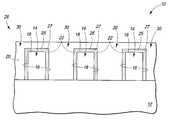
- a substrate fragmentis indicated generally with reference numeral 10 .
- Suchmay comprise a semiconductor or other substrate.
- the term “semiconductor substrate” or “semiconductive substrate”is defined to mean any construction comprising semiconductive material, including, but not limited to, bulk semiconductive materials such as a semiconductive wafer (either alone or in assemblies comprising other materials thereon), and semiconductive material layers (either alone or in assemblies comprising other materials).
- substraterefers to any supporting structure, including, but not limited to, the semiconductive substrates described above.
- Substrate fragment 10comprises substrate material 12 , for example which may be homogenous or non-homogenous and include any of conductive, semiconductive, and insulating materials. Such might, for example, be used in the fabrication of integrated circuitry.
- Spaced first features 14have been formed over substrate 12 , and may also be homogenous or non-homogenous. Such may be partially or wholly sacrificial, and accordingly may or may not comprise a part of a finished circuitry construction where circuitry is being fabricated.
- Spaced first features 14may be fabricated by any existing or yet-to-be developed technique. Examples include lithography, for example photolithography. Spaced first features 14 may be patterned at, greater than, or less than the minimum photolithographic resolution with which substrate 10 is fabricated.
- Spaced first features 14are shown as being of the same shape and spacing relative one another and as being generally rectangular in cross-section. Other shapes, differing shapes among the features, and two or more different spacings may be used. Individual of the spaced first features 14 may be considered as comprising opposing lateral sidewalls 16 and an elevationally outermost top wall or surface 18 . In one embodiment, sidewalls 16 are generally parallel one another. In one embodiment, sidewalls 16 are generally parallel one another and extend generally orthogonally relative to substrate 12 .
- material 20has been formed onto opposing lateral sidewalls 16 of spaced first features 14 , and over elevationally outermost surfaces/top walls 18 of spaced first features 14 .
- Material 20may or may not be homogenous, and regardless may or may not form a part of finished integrated circuitry construction where integrated circuitry is being fabricated. Regardless, that portion of material 20 which is received against each of opposing lateral sidewalls 16 is of different composition from composition of each of opposing lateral sidewalls 16 . Further, where material 20 is received over and against elevationally outermost surfaces/top walls 18 , that portion of material 20 which is received against a surface/wall 18 may be of different composition from composition of surface/wall 18 .
- material 20 and spaced first features 14may be considered as contacting against one another at respective interfaces 22 . Example compositions for those portions of material 20 and spaced first features 14 contacting at such interfaces 22 are described in more detail below.
- FIGS. 3 and 4at least one of the portion of material 20 received against lateral sidewalls 16 and the spaced first features 14 is densified to move at least one of such portion of material 20 or spaced first features 14 away from the other to form a void space 25 between each of opposing lateral sidewalls 16 and the portion of material 20 previously received there-against.
- FIGS. 3 and 4depict an example embodiment wherein both material 20 and spaced first features 14 have been densified such that material of each moves laterally away from interfaces 22 .
- FIG. 3also depicts densifying at least one of the portions of material 20 against top walls 18 or spaced features 14 such that void spaces 25 extend across and over top walls 18 of each spaced first feature 14 .
- substrate 10has been treated to form void space 25 to be of an upside-down generally U-shape (having a base 27 ), and received about each of spaced first features 14 in the example depicted cross-section.
- Composition of material 20 and/or composition of the material of spaced first features 14 after the densificationmay be the same or different from such compositions prior to densification of either.
- the void space which is formedmay be received only between one lateral sidewall 16 or both lateral sidewalls 16 and portion(s) of material 20 previously received there-against without being formed atop features 14 .
- FIG. 3depicts an example pattern 28 formed over substrate 12 .
- Pattern 28may be considered as comprising interconnected spaced second features 30 which comprise material 20 , with spaced second features 30 being spaced from and received between spaced first features 14 .
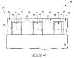
- FIGS. 5 and 6depict alternate example embodiment substrate fragments 10 a and 10 b .
- Like numerals from the first described embodimenthave been used where appropriate, with some construction differences being indicated with the suffix “a” and “b”, respectively.
- FIG. 5depicts an example wherein only that portion of material 20 previously received at interface 22 has moved laterally away from the other of spaced first feature material 14 a to form void space 25 a .
- FIG. 6depicts an example wherein only spaced first feature material 14 previously received at interface 22 has moved laterally away from interface 22 . Accordingly, the act of densifying and moving to form void space 25 a or 25 b results from densification and movement of only one material relative to the other, as opposed to both as shown in the embodiment of FIGS. 3 and 4 .
- FIG. 7depicts another example embodiment substrate fragment 10 c .
- material of spaced first features 14 chas actually expanded, thereby reducing its density, and moved toward the portion of material 20 which was previously received at interface 22 .
- the densification of material 20has been greater than the expansion of material of feature 14 c such that a void space 25 c forms.
- Suchmay of course be reversed, for example wherein material 20 is caused to expand and material 14 is caused to densify (not shown) at a greater rate than the expansion of material 20 to form a void space.
- Different compositionsmay be selected by the artisan for material 20 and that of spaced first features 14 to enable densification of one or both materials relative to the other such that a void space is created. Further, depending on the materials chosen, densification may be achieved in different manners. For example, one or both of the spaced first features 14 and material 20 may comprise different composition photoresists. Densification of one or both relative to the other to create a void space may, for example, occur by actinically irradiating the example substrate of FIG. 2 , and/or densification may occur by heating the substrate of FIG. 2 . Ideally, densification occurs in the absence of any etching of material of substrate 10 such that void formation occurs by densification alone.
- first features 14may comprise any suitable photoresist, with material 20 formed thereover comprising polymethylmethacrylate.
- heating the substrate of FIG. 2 comprised of polymethylmethacrylate 20 and photoresist 14 at a temperature of at least 50° C. (ideally from 100° C. to 130° C.) for approximately 60 seconds to 90 secondswill cause densification of either, and commensurate formation of void space 25 .
- first features 14are resist, or any polymer, such may or may not be treated prior to forming material 20 there-over such that the treatment renders first features 14 insoluble in the solvent from which material 20 is solvent (spin) cast, if material 20 is solvent cast.
- Example treatmentsinclude conventional resist “freezing” techniques used in double patterning, e.g. thermal cross-linking, photo cross-linking, thermal generation of acid followed by photo-induced acid catalyzed polymerization, or formation of a protective encapsulation layer over first features 14 , for example forming an insoluble chemical coating or forming a thin insoluble coating by atomic layer deposition of, for example, oxide.
- Densification with commensurate volume changemay also occur by reaction of certain materials, for example by thermolytic cleavage or acid hydrolysis of material, such as in transformation of polytert-butyl acrylate to polyacrylic acid.
- Other example materials which undergo densification and volume change upon reactioninclude thermally curable epoxy resins, for example vinyl esters, unsaturated polyesters, and blends thereof. Such may, for example, be cured with suitable elevated temperatures at or below 100° C. Other epoxy resins and blends thereof may be cured at, for example, higher temperatures from 120° C. to 500° C.
- first features 14may not comprise photoresist or other material not capable of being processed at such temperatures without melting. Accordingly in such instances, spaced first features 14 might be fabricated of any suitable, existing, or yet-to-be developed hardmask material which itself was previously patterned utilizing photolithography and/or in other manner.
- Densification and commensurate volume changemay also occur by actinic irradiation, such as by photo-polymerization of acrylate or epoxy monomers or prepolymers in the presence of photo-activated radicals or cationic initiators.
- actinic irradiationsuch as by photo-polymerization of acrylate or epoxy monomers or prepolymers in the presence of photo-activated radicals or cationic initiators.
- urethane dimethacrylateis photo-polymerized with visible light to impart a densification and volume shrinking of 5.3%.
- the monomers or prepolymersmay themselves be photosensitive and a separate initiator species may not be present. Examples include fully imidized, soluble, auto-photosensitive polyimides. Regardless, example such photoresists may be positive or negative.
- certain positive photoresistsmay be caused to shrink due to outgassing of byproducts of the photochemical process, including removal of protecting groups from the resist molecule.
- An exampleis deprotection of tert-butoxycarbonyl, acetal, or tert-butyl acrylate groups, including copolymers thereof, for example comprised of hydroxystyrene monomers.
- the photo or acid cleaved protecting groupmay outgas from the resist film during either exposure and/or post-exposure bake.
- Additional examples of densification of positive photoresist by out-gassinginclude formation of byproducts in the photoacid generation process in chemically amplified resists.
- Examplesinclude where the photoacid generator molecule is an onium salt, for example sulfonium perfluorosulfonate, and wherein the anion generated during photolysis and remains of the reacted cation may outgas from the resist film during either exposure and/or post-exposure bake.
- the photoacid generator moleculeis an onium salt, for example sulfonium perfluorosulfonate, and wherein the anion generated during photolysis and remains of the reacted cation may outgas from the resist film during either exposure and/or post-exposure bake.
- thermo-responsive polymer gelsfor example hydrogels such as poly (N-isopropylacrylamide).
- Thermo-responsive hydrogelsswell below and shrink above their lower critical solution temperature.
- poly(N-isopropylacrylamide)such occurs due to a reversible formation and cleavage of hydrogen bonds between NH or C ⁇ O groups and the surrounding water molecules with changing temperature.
- Other hydrogel trigger stimuliother than temperature for certain thermo-responsive hydrogels include electric field, pH, and/or third-body solute concentration.
- Additional example materialsinclude those which may be thermally shrunk, such as shrink-wrap materials. Such materials may be deposited with stretching provided via sheer thinning during film casting.
- Example materialsinclude linear molecules like polyvinylchloride or polyolefins such as polyethylene.
- Additional examplesinclude segmented block copolymers and elastomer-plastic blends, for example a copolymer of ethylene and vinyl acetate, including blends thereof. Densification and commensurate volume change to form voids may occur during a post-coat thermal bake where, for example, mobility is imparted to the stretched polymer molecules and they contract to an equilibrium coiled configuration.
- Additional example materials which may be treated to impart densification and thereby volume change to form a void spaceinclude reversibly doped conjugated polymers, for example polypyrrole. Such materials undergo reversible volume change during doping and undoping thereof.
- an electrically conducting reversibly doped conjugated polymersuch as polypyrrole may be submersed in an electrolyte solution.
- a suitable voltageelectric field
- ionsare exchanged between the polymer and electrolyte.
- the polymerundergoes a volume change by densification up to several percent.
- the volume changeis primarily due to physical separation of the chains due to dopant insertion or extraction. If ions are expelled from the polymer, it shrinks and increases in density.
- various of the above materials and techniquesmay be selected at least for those portions of spaced first features 14 and material 20 which come into contact relative to one another at interfaces 22 to result in desired formation of suitable void spaces 25 / 25 a / 25 b / 25 c .
- interface 22 where void formation nucleatesideally promotes dewetting or separation during the shrinking process, or at least does not encompass strong adhesion of one material relative to the other.
- interfaces where void formation nucleatesare ideally chemically specific so as to promote dewetting or separation of the different composition materials during the densification process.
- opposing lateral sidewalls 16 and/or top wall 18may be treated prior to or during deposition of material 20 thereover.
- Chemical tailoring of surfaces 16 / 18may include selective fluorocarbon polymer formation via fluorine plasma etching. Further, diffusion and surface migration of fluorinated components of many photoresist materials will inherently facilitate dewetting or separation. Additionally or alternately, functionalized self-assembled monomers may be selectively deposited onto the surfaces of spaced first features 14 prior to deposition of material 20 . Ideally, the interface between the shrinking material(s) and the underlying substrate is such that the contact angle between the shrinking material and the underlying substrate is approximately 90°, which may or may not be achieved through separate chemical functionalization of the material(s) which will be densified.
- FIG. 3depicts an example wherein void space 25 upon initial formation is sealed elevationally outward by material 22 in the depicted cross-section.
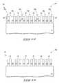
- FIG. 8some of material 20 has been removed to open void spaces 25 elevationally outward after their initial formation. Such forms a pattern 32 wherein spaced second features 30 are disconnected and spaced from and alternate with spaced first features 14 . Accordingly, FIG. 8 depicts modification of pattern 28 of FIG. 3 to form a pattern 32 on substrate 12 . Regardless, alternate processing may occur.
- FIGS. 2-4depict an embodiment wherein material 20 is received elevationally over outermost surfaces 18 of spaced first features 14 during the act of densification to form void spaces 25 .
- material 20may be removed from being received over elevationally outermost surfaces of spaced first features 14 during the densification.
- FIG. 9depicts a substrate fragment 10 d .
- Like numerals from the first-described embodimenthave been utilized where appropriate, with some construction differences being indicated with the suffix “d”. Such depicts subsequent processing to that depicted by FIG. 2 wherein material 20 has been chemically etched, polished, or otherwise removed inwardly at least to elevationally outermost surfaces 18 of spaced first features 14 . Densification of the FIG.
- void spaces 25 which are createdare open elevationally outward in cross-section upon initial formation, which for example would occur when no material is received over elevationally outermost surfaces 18 of spaced first features 14 during the densification.
- Pattern 32 formed over substrate 10may or may not comprise a part of the finished construction of substrate 10 . Further, pattern 32 may be subsequently modified, regardless. For example, one or both of spaced first features 14 and spaced second features 30 of FIG. 8 may be laterally trimmed to reduce their respective widths.
- FIG. 10depicts an example embodiment pattern 34 wherein the respective widths of each of spaced second features 30 and spaced first features 14 has been laterally trimmed (for example by suitable wet and/or dry chemical etching) to reduce their respective widths. Depending upon composition of spaced first features 14 and spaced second features 30 in FIG. 8 , the FIG. 10 lateral trimming may occur at the same time using a single chemistry.
- the lateral trimming of spaced first features 14 and spaced second features 30may occur at different times using different etching chemistries, with such act of lateral trimming occurring with respect to either before the other. Further, only one or neither of such spaced features may be trimmed. Further, spaced first features 14 of FIG. 1 may be laterally trimmed after formation and prior to deposition of material 20 thereover.
- Embodiments of the inventionmay also comprise processing the substrate through a mask pattern which comprises the spaced first features and the material from which the spaced second features are formed.
- FIG. 11depicts one such example wherein substrate 10 has been processed by etching through a mask pattern comprised of pattern 34 to etch into material 12 .
- Any alternate existing or yet-to-be developed processingmight also or alternately be conducted, for example doping, ion implanting, selective deposition, etc.
- a substrate 10 e in FIGS. 12-15is next described with respect to a substrate 10 e in FIGS. 12-15 .
- Like numerals from the first-described embodimenthave been utilized where appropriate, with some construction differences being indicated with the suffix “e” or with different numerals.
- a pattern 34 ehas been formed which comprises spaced first features 14 e and spaced second features 30 e . Such may be manufactured in accordance with any of the above-described techniques with respect to spaced first features 14 and spaced second features 30 .
- a spacer-forming layer 40has been deposited over features 14 e and 30 e .
- Suchmay comprise a material from which features 14 e and features 30 e may be selectively etched.
- a selective etchrequires removal of one material relative to another at a rate of at least 2:1.
- Spacer-forming layer 40has been deposited to a thickness which less than fills the space between immediately adjacent of spacers 14 e and 30 e.
- spacer-forming layer 40has been anisotropically etched to form spaced spacers 42 over lateral sidewalls of the materials of first features 14 e and second features 30 e.
- a pattern 44has been formed on substrate 12 . Such may or may not be used as a mask pattern in the subsequent processing of substrate 12 there-through.
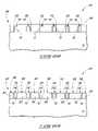
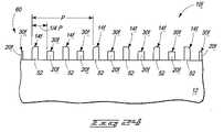
- FIG. 16depicts formation of spaced mask features 50 , for example comprising, consisting essentially of, or consisting of photoresist.
- Mask features 50have been fabricated over substrate 12 in a repeating pattern of a pitch “P”.
- Mask features 50may comprise material other than photoresist. Regardless, pitch P may be equal to, greater than, or less than the minimum photolithographic resolution with which substrate 10 f is fabricated.
- mask features 50have been laterally trimmed to reduce their respective widths.
- a spacer-forming layer 52has been deposited over substrate 12 , including over spaced features 50 .
- spacer-forming layer 52has been anisotropically etched to form spaced first features 14 f about sidewalls of spaced features 50 .
- spaced features 50(not shown) have been removed from the substrate selectively relative to spaced first features 14 f.
- material 20 fhas been formed.
- Material 52 of spaced first features 14 f and material 20 fcorrespond in composition to that of materials 14 and 20 as described above.
- At least one of the portion of material 20 f adjacent material 52 and spaced first features 14 fhave been densified to be moved laterally away from the interface thereof. Such forms a void space 25 f which is at least received between each of the opposing lateral sidewalls of spaced first features 14 f and material 20 f , and forms a pattern 28 f.
- material 20 fhas been laterally trimmed to reduce its respective widths.
- Spaced first features 14 fare shown as not having been laterally trimmed.
- a pattern 60is depicted as being formed over substrate 12 .
- Pattern 60is depicted as having a pitch which is one fourth (an integer factor of 4) that of pitch “P” of spaced mask features 50 in FIG. 16 .
- any degree of pitch reductionin any of the above-described embodiments, if occurring, will of course be in large part determined on the degree of any lateral trimming that may occur of the respective spaced features in combination with thickness of the deposited layers to produce the features and spaces between the features.
Landscapes
- Physics & Mathematics (AREA)
- General Physics & Mathematics (AREA)
- Engineering & Computer Science (AREA)
- Condensed Matter Physics & Semiconductors (AREA)
- Manufacturing & Machinery (AREA)
- Computer Hardware Design (AREA)
- Microelectronics & Electronic Packaging (AREA)
- Power Engineering (AREA)
- Internal Circuitry In Semiconductor Integrated Circuit Devices (AREA)
- Element Separation (AREA)
- Drying Of Semiconductors (AREA)
- Preparing Plates And Mask In Photomechanical Process (AREA)
- Micromachines (AREA)
- Manufacturing Of Printed Wiring (AREA)
- Shaping Of Tube Ends By Bending Or Straightening (AREA)
- Exposure Of Semiconductors, Excluding Electron Or Ion Beam Exposure (AREA)
Abstract
Description
Claims (35)
Priority Applications (8)
| Application Number | Priority Date | Filing Date | Title |
|---|---|---|---|
| US12/409,308US8268543B2 (en) | 2009-03-23 | 2009-03-23 | Methods of forming patterns on substrates |
| PCT/US2010/025495WO2010110987A2 (en) | 2009-03-23 | 2010-02-26 | Methods of forming patterns on substrates |
| KR1020117024878AKR101327577B1 (en) | 2009-03-23 | 2010-02-26 | Methods of forming patterns on substrates |
| EP10756541.8AEP2412004B1 (en) | 2009-03-23 | 2010-02-26 | Methods of forming patterns on substrates |
| CN201080013110.1ACN102362334B (en) | 2009-03-23 | 2010-02-26 | Method of forming a pattern on a substrate |
| JP2012502066AJP5516717B2 (en) | 2009-03-23 | 2010-02-26 | Method for forming a pattern on a substrate |
| TW099107690ATWI396227B (en) | 2009-03-23 | 2010-03-16 | Methods of forming patterns on substrates |
| US13/483,339US8563228B2 (en) | 2009-03-23 | 2012-05-30 | Methods of forming patterns on substrates |
Applications Claiming Priority (1)
| Application Number | Priority Date | Filing Date | Title |
|---|---|---|---|
| US12/409,308US8268543B2 (en) | 2009-03-23 | 2009-03-23 | Methods of forming patterns on substrates |
Related Child Applications (1)
| Application Number | Title | Priority Date | Filing Date |
|---|---|---|---|
| US13/483,339ContinuationUS8563228B2 (en) | 2009-03-23 | 2012-05-30 | Methods of forming patterns on substrates |
Publications (2)
| Publication Number | Publication Date |
|---|---|
| US20100239983A1 US20100239983A1 (en) | 2010-09-23 |
| US8268543B2true US8268543B2 (en) | 2012-09-18 |
Family
ID=42737962
Family Applications (2)
| Application Number | Title | Priority Date | Filing Date |
|---|---|---|---|
| US12/409,308Active2030-03-25US8268543B2 (en) | 2009-03-23 | 2009-03-23 | Methods of forming patterns on substrates |
| US13/483,339ActiveUS8563228B2 (en) | 2009-03-23 | 2012-05-30 | Methods of forming patterns on substrates |
Family Applications After (1)
| Application Number | Title | Priority Date | Filing Date |
|---|---|---|---|
| US13/483,339ActiveUS8563228B2 (en) | 2009-03-23 | 2012-05-30 | Methods of forming patterns on substrates |
Country Status (7)
| Country | Link |
|---|---|
| US (2) | US8268543B2 (en) |
| EP (1) | EP2412004B1 (en) |
| JP (1) | JP5516717B2 (en) |
| KR (1) | KR101327577B1 (en) |
| CN (1) | CN102362334B (en) |
| TW (1) | TWI396227B (en) |
| WO (1) | WO2010110987A2 (en) |
Families Citing this family (10)
| Publication number | Priority date | Publication date | Assignee | Title |
|---|---|---|---|---|
| US8791447B2 (en) | 2011-01-20 | 2014-07-29 | Micron Technology, Inc. | Arrays of nonvolatile memory cells and methods of forming arrays of nonvolatile memory cells |
| US20140110805A1 (en)* | 2012-10-18 | 2014-04-24 | Infineon Technologies Dresden Gmbh | Silicon light trap devices, systems and methods |
| US8956808B2 (en)* | 2012-12-04 | 2015-02-17 | Globalfoundries Inc. | Asymmetric templates for forming non-periodic patterns using directed self-assembly materials |
| US9213239B2 (en) | 2013-01-22 | 2015-12-15 | Micron Technology, Inc. | Methods of forming patterns for semiconductor device structures |
| US8790522B1 (en) | 2013-02-11 | 2014-07-29 | Globalfoundries Inc. | Chemical and physical templates for forming patterns using directed self-assembly materials |
| US8999623B2 (en) | 2013-03-14 | 2015-04-07 | Wiscousin Alumni Research Foundation | Degradable neutral layers for block copolymer lithography applications |
| US9583381B2 (en) | 2013-06-14 | 2017-02-28 | Micron Technology, Inc. | Methods for forming semiconductor devices and semiconductor device structures |
| KR102323456B1 (en)* | 2014-12-26 | 2021-11-10 | 삼성전자주식회사 | A semiconductor device and method for fabricating the semiconductor device |
| US10147611B1 (en)* | 2017-08-28 | 2018-12-04 | Nanya Technology Corporation | Method for preparing semiconductor structures |
| WO2023091734A1 (en)* | 2021-11-22 | 2023-05-25 | Meta Platforms Technologies, Llc | Tunable shrinkage and trim process for fabricating gratings |
Citations (179)
| Publication number | Priority date | Publication date | Assignee | Title |
|---|---|---|---|---|
| EP0171111A2 (en) | 1984-07-13 | 1986-02-12 | BELL TELEPHONE MANUFACTURING COMPANY Naamloze Vennootschap | Process to superpose two positive photoresist layers |
| US5047117A (en) | 1990-09-26 | 1991-09-10 | Micron Technology, Inc. | Method of forming a narrow self-aligned, annular opening in a masking layer |
| US5254218A (en) | 1992-04-22 | 1993-10-19 | Micron Technology, Inc. | Masking layer having narrow isolated spacings and the method for forming said masking layer and the method for forming narrow isolated trenches defined by said masking layer |
| US5328810A (en) | 1990-05-07 | 1994-07-12 | Micron Technology, Inc. | Method for reducing, by a factor or 2-N, the minimum masking pitch of a photolithographic process |
| US5372916A (en) | 1991-09-12 | 1994-12-13 | Hitachi, Ltd. | X-ray exposure method with an X-ray mask comprising phase shifter sidewalls |
| US5382315A (en) | 1991-02-11 | 1995-01-17 | Microelectronics And Computer Technology Corporation | Method of forming etch mask using particle beam deposition |
| US5420067A (en) | 1990-09-28 | 1995-05-30 | The United States Of America As Represented By The Secretary Of The Navy | Method of fabricatring sub-half-micron trenches and holes |
| US5429988A (en) | 1994-06-13 | 1995-07-04 | United Microelectronics Corporation | Process for producing high density conductive lines |
| US5573837A (en) | 1992-04-22 | 1996-11-12 | Micron Technology, Inc. | Masking layer having narrow isolated spacings and the method for forming said masking layer and the method for forming narrow isolated trenches defined by said masking layer |
| US5593813A (en) | 1994-07-14 | 1997-01-14 | Hyundai Electronics Industries Co. Ltd. | Method for forming submicroscopic patterns |
| US5905279A (en) | 1996-04-09 | 1999-05-18 | Kabushiki Kaisha Toshiba | Low resistant trench fill for a semiconductor device |
| US6063688A (en) | 1997-09-29 | 2000-05-16 | Intel Corporation | Fabrication of deep submicron structures and quantum wire transistors using hard-mask transistor width definition |
| US6087263A (en) | 1998-01-29 | 2000-07-11 | Micron Technology, Inc. | Methods of forming integrated circuitry and integrated circuitry structures |
| US6140217A (en) | 1998-07-16 | 2000-10-31 | International Business Machines Corporation | Technique for extending the limits of photolithography |
| US6207490B1 (en) | 1997-12-11 | 2001-03-27 | Samsung Electronics Co., Ltd. | Semiconductor device and method for fabricating the same |
| US6249335B1 (en) | 1992-01-17 | 2001-06-19 | Nikon Corporation | Photo-mask and method of exposing and projection-exposing apparatus |
| US20020037617A1 (en) | 2000-06-29 | 2002-03-28 | Kim Jun Dong | Method for forming gate electrodes in a semicoductor device using formed fine patterns |
| US6383952B1 (en) | 2001-02-28 | 2002-05-07 | Advanced Micro Devices, Inc. | RELACS process to double the frequency or pitch of small feature formation |
| US20020094688A1 (en) | 2001-01-16 | 2002-07-18 | Semiconductor Leading Edge Technologies, Inc. | Method of forming fine patterns |
| US6483136B1 (en) | 1997-06-20 | 2002-11-19 | Hitachi, Ltd. | Semiconductor integrated circuit and method of fabricating the same |
| US20030006410A1 (en)* | 2000-03-01 | 2003-01-09 | Brian Doyle | Quantum wire gate device and method of making same |
| US6545904B2 (en) | 2001-03-16 | 2003-04-08 | Micron Technology, Inc. | 6f2 dram array, a dram array formed on a semiconductive substrate, a method of forming memory cells in a 6f2 dram array and a method of isolating a single row of memory cells in a 6f2 dram array |
| US6548401B1 (en) | 2002-01-23 | 2003-04-15 | Micron Technology, Inc. | Semiconductor processing methods, and semiconductor constructions |
| US20030091936A1 (en) | 2001-08-31 | 2003-05-15 | Jorg Rottstegge | Process for sidewall amplification of resist structures and for the production of structures having reduced structure size |
| US6566280B1 (en) | 2002-08-26 | 2003-05-20 | Intel Corporation | Forming polymer features on a substrate |
| US6580136B2 (en) | 2001-01-30 | 2003-06-17 | International Business Machines Corporation | Method for delineation of eDRAM support device notched gate |
| KR20030049198A (en) | 2001-12-14 | 2003-06-25 | 주식회사 하이닉스반도체 | Forming method of photoresist pattern improving etching resistance by relacs material |
| KR20030056601A (en) | 2001-12-28 | 2003-07-04 | 주식회사 하이닉스반도체 | Method of forming a source line in flash memory device |
| US6599844B2 (en) | 2000-06-22 | 2003-07-29 | Hyundai Electronics Industries, Co., Ltd. | Method and forming fine patterns of semiconductor devices using passivation layers |
| US6605541B1 (en) | 1998-05-07 | 2003-08-12 | Advanced Micro Devices, Inc. | Pitch reduction using a set of offset masks |
| JP2003234279A (en) | 2002-02-08 | 2003-08-22 | Sony Corp | Forming method of resist pattern, manufacturing method of semiconductor device and forming device for resist pattern |
| US6627524B2 (en) | 2001-06-06 | 2003-09-30 | Micron Technology, Inc. | Methods of forming transistor gates; and methods of forming programmable read-only memory constructions |
| US6630379B2 (en) | 2000-06-23 | 2003-10-07 | International Business Machines Corporation | Method of manufacturing 6F2 trench capacitor DRAM cell having vertical MOSFET and 3F bitline pitch |
| US6638441B2 (en) | 2002-01-07 | 2003-10-28 | Macronix International Co., Ltd. | Method for pitch reduction |
| KR20030089063A (en) | 2002-05-16 | 2003-11-21 | 주식회사 하이닉스반도체 | Forming method of photoresist pattern |
| US6667502B1 (en) | 1999-08-31 | 2003-12-23 | Micron Technology, Inc. | Structurally-stabilized capacitors and method of making of same |
| US6703323B2 (en) | 2001-12-14 | 2004-03-09 | Hynix Semiconductor Inc | Method of inhibiting pattern collapse using a relacs material |
| US6710390B2 (en) | 1997-07-03 | 2004-03-23 | Micron Technology, Inc. | Capacitors and DRAM arrays |
| US6735132B2 (en) | 2001-07-23 | 2004-05-11 | Micron Technology, Inc. | 6F2 DRAM array with apparatus for stress testing an isolation gate and method |
| US6753220B2 (en) | 1996-11-01 | 2004-06-22 | Micron Technology, Inc. | Semiconductor processing methods of forming devices on a substrate, forming device arrays on a substrate, forming conductive lines on a substrate, and forming capacitor arrays on a substrate, and integrated circuitry |
| US6756619B2 (en) | 2002-08-26 | 2004-06-29 | Micron Technology, Inc. | Semiconductor constructions |
| KR20040057582A (en) | 2002-12-26 | 2004-07-02 | 주식회사 하이닉스반도체 | Method of forming a micro pattern having a dual damascene |
| JP2004247399A (en) | 2003-02-12 | 2004-09-02 | Renesas Technology Corp | Method for manufacturing semiconductor device |
| US20040198065A1 (en)* | 2003-04-04 | 2004-10-07 | Sung-Kwon Lee | Method for fabricating semiconductor device with fine patterns |
| US6826069B2 (en) | 2001-03-14 | 2004-11-30 | Atmos Corporation | Interleaved wordline architecture |
| US6864184B1 (en) | 2004-02-05 | 2005-03-08 | Advanced Micro Devices, Inc. | Method for reducing critical dimension attainable via the use of an organic conforming layer |
| US6872512B2 (en) | 2002-03-27 | 2005-03-29 | Nec Lcd Technologies, Ltd. | Method of forming resist pattern |
| US6905975B2 (en) | 2003-07-03 | 2005-06-14 | Micron Technology, Inc. | Methods of forming patterned compositions |
| US20050130068A1 (en) | 2003-11-21 | 2005-06-16 | Takehiro Kondoh | Pattern forming method and method for manufacturing a semiconductor device |
| US6916594B2 (en) | 2002-12-30 | 2005-07-12 | Hynix Semiconductor Inc. | Overcoating composition for photoresist and method for forming photoresist pattern using the same |
| US20050164478A1 (en) | 2004-01-26 | 2005-07-28 | Taiwan Semiconductor Manufacturing Co. | Novel method of trimming technology |
| US20050173740A1 (en) | 2004-02-07 | 2005-08-11 | You-Seung Jin | Multi-gate transistor formed with active patterns of uniform critical dimension |
| US6951822B2 (en) | 2001-09-28 | 2005-10-04 | Infineon Technologies North America Corp. | Method for forming inside nitride spacer for deep trench device DRAM cell |
| US20050255696A1 (en) | 2003-05-09 | 2005-11-17 | Fujitsu Limited | Method of processing resist, semiconductor device, and method of producing the same |
| US20050272220A1 (en) | 2004-06-07 | 2005-12-08 | Carlo Waldfried | Ultraviolet curing process for spin-on dielectric materials used in pre-metal and/or shallow trench isolation applications |
| US20060011947A1 (en) | 2004-05-26 | 2006-01-19 | Werner Juengling | Semiconductor structures and memory device constructions |
| US20060046484A1 (en) | 2004-09-02 | 2006-03-02 | Abatchev Mirzafer K | Method for integrated circuit fabrication using pitch multiplication |
| US20060046422A1 (en) | 2004-08-31 | 2006-03-02 | Micron Technology, Inc. | Methods for increasing photo alignment margins |
| US20060046200A1 (en) | 2004-09-01 | 2006-03-02 | Abatchev Mirzafer K | Mask material conversion |
| CN1761063A (en) | 2004-10-14 | 2006-04-19 | 茂德科技股份有限公司 | Structure of Dynamic Random Access Memory |
| US20060088788A1 (en) | 2004-10-26 | 2006-04-27 | Takanori Kudo | Composition for coating over a photoresist pattern |
| US7037840B2 (en) | 2004-01-26 | 2006-05-02 | Micron Technology, Inc. | Methods of forming planarized surfaces over semiconductor substrates |
| US7049652B2 (en) | 2003-12-10 | 2006-05-23 | Sandisk Corporation | Pillar cell flash memory technology |
| US20060115978A1 (en) | 2004-11-30 | 2006-06-01 | Michael Specht | Charge-trapping memory cell and method for production |
| US20060118785A1 (en) | 2003-09-12 | 2006-06-08 | International Business Machines Corporation | Techniques for patterning features in semiconductor devices |
| US7064376B2 (en) | 1996-05-24 | 2006-06-20 | Jeng-Jye Shau | High performance embedded semiconductor memory devices with multiple dimension first-level bit-lines |
| US7067385B2 (en) | 2003-09-04 | 2006-06-27 | Micron Technology, Inc. | Support for vertically oriented capacitors during the formation of a semiconductor device |
| US20060154182A1 (en) | 2005-01-12 | 2006-07-13 | International Business Machines Corporation | Method for post lithographic critical dimension shrinking using post overcoat planarization |
| JP2006245625A (en) | 1997-06-20 | 2006-09-14 | Hitachi Ltd | Semiconductor integrated circuit device and manufacturing method thereof |
| US7125781B2 (en) | 2003-09-04 | 2006-10-24 | Micron Technology, Inc. | Methods of forming capacitor devices |
| US20060240361A1 (en) | 2005-04-21 | 2006-10-26 | Ji-Young Lee | Method of forming small pitch pattern using double spacers |
| US20060273456A1 (en) | 2005-06-02 | 2006-12-07 | Micron Technology, Inc., A Corporation | Multiple spacer steps for pitch multiplication |
| US20060278911A1 (en) | 2005-06-14 | 2006-12-14 | Eppich Anton P | Relaxed-pitch method of aligning active area to digit line |
| US20060286795A1 (en) | 2005-06-21 | 2006-12-21 | Kabushiki Kaisha Toshiba | Method of manufacturing semiconductor device |
| US20070003878A1 (en) | 2005-03-23 | 2007-01-04 | Asml Netherlands B.V. | Reduced pitch multiple exposure process |
| US20070010058A1 (en) | 2005-07-08 | 2007-01-11 | Micron Technology, Inc. | Method and apparatus for a self-aligned recessed access device (RAD) transistor gate |
| US7166533B2 (en) | 2005-04-08 | 2007-01-23 | Infineon Technologies, Ag | Phase change memory cell defined by a pattern shrink material process |
| US20070020565A1 (en) | 2005-07-25 | 2007-01-25 | Samsung Electronics Co., Ltd. | Methods of fabricating a semiconductor device |
| US20070023805A1 (en) | 2005-07-26 | 2007-02-01 | Wells David H | Reverse construction memory cell |
| US20070026684A1 (en) | 2005-08-01 | 2007-02-01 | Stefano Parascandola | Method of producing pitch fractionizations in semiconductor technology |
| US20070037066A1 (en) | 2005-08-09 | 2007-02-15 | Li-Tung Hsiao | Method for correcting and configuring optical mask pattern |
| US20070049030A1 (en) | 2005-09-01 | 2007-03-01 | Sandhu Gurtej S | Pitch multiplication spacers and methods of forming the same |
| US20070048930A1 (en) | 2005-09-01 | 2007-03-01 | Figura Thomas A | Peripheral gate stacks and recessed array gates |
| US20070045712A1 (en) | 2005-09-01 | 2007-03-01 | Haller Gordon A | Memory cell layout and process flow |
| US20070049035A1 (en) | 2005-08-31 | 2007-03-01 | Tran Luan C | Method of forming pitch multipled contacts |
| US20070049011A1 (en) | 2005-09-01 | 2007-03-01 | Micron Technology, Inc., A Corporation | Method of forming isolated features using pitch multiplication |
| US20070049003A1 (en) | 2005-09-01 | 2007-03-01 | John Smythe | Semiconductor constructions and methods of forming layers |
| US20070048674A1 (en) | 2005-09-01 | 2007-03-01 | Wells David H | Methods for forming arrays of small, closely spaced features |
| US20070049040A1 (en) | 2005-03-15 | 2007-03-01 | Micron Technology, Inc., A Corporation | Multiple deposition for integration of spacers in pitch multiplication process |
| US7199005B2 (en) | 2005-08-02 | 2007-04-03 | Micron Technology, Inc. | Methods of forming pluralities of capacitors |
| US20070077743A1 (en) | 2005-09-30 | 2007-04-05 | Rao Rajesh A | Multiple fin formation |
| US20070077524A1 (en) | 2005-09-30 | 2007-04-05 | Samsung Electronics Co., Ltd. | Method for forming patterns of semiconductor device |
| US7202174B1 (en) | 2006-02-02 | 2007-04-10 | Hynix Semiconductor Inc. | Method of forming micro pattern in semiconductor device |
| US7202127B2 (en) | 2004-08-27 | 2007-04-10 | Micron Technology, Inc. | Methods of forming a plurality of capacitors |
| US20070085152A1 (en) | 2005-10-14 | 2007-04-19 | Promos Technologies Pte.Ltd. Singapore | Reduced area dynamic random access memory (DRAM) cell and method for fabricating the same |
| US20070096182A1 (en) | 2004-09-10 | 2007-05-03 | Infineon Technologies Ag | Transistor, meomory cell array and method of manufacturing a transistor |
| US20070099431A1 (en) | 2005-11-01 | 2007-05-03 | Micron Technology, Inc. | Process for increasing feature density during the manufacture of a semiconductor device |
| US20070105357A1 (en) | 2005-09-01 | 2007-05-10 | Micron Technology, Inc. | Silicided recessed silicon |
| US20070123015A1 (en) | 2005-11-30 | 2007-05-31 | International Business Machines Corporation | Passive components in the back end of integrated circuits |
| US7230292B2 (en) | 2003-08-05 | 2007-06-12 | Micron Technology, Inc. | Stud electrode and process for making same |
| US20070145464A1 (en) | 2002-08-29 | 2007-06-28 | Voshell Thomas W | Random access memory device utilizing a vertically oriented select transistor |
| US20070161251A1 (en) | 2005-03-15 | 2007-07-12 | Micron Technology, Inc. | Pitch reduced patterns relative to photolithography features |
| US20070181929A1 (en) | 2005-06-27 | 2007-08-09 | Micron Technology, Inc. | Semiconductor Constructions, Memory Cells, DRAM Arrays, Electronic Systems; Methods of Forming Semiconductor Constructions; and Methods of Forming DRAM Arrays |
| US20070190463A1 (en) | 2004-09-02 | 2007-08-16 | Micron Technology, Inc. | Method to align mask patterns |
| US20070197014A1 (en) | 2006-02-17 | 2007-08-23 | Samsung Electronics Co., Ltd. | Method of fabricating semiconductor device |
| US20070202671A1 (en) | 2006-02-24 | 2007-08-30 | Hynix Semiconductor Inc. | Method for forming fine pattern of semiconductor device |
| US20070202697A1 (en)* | 2006-02-24 | 2007-08-30 | Hynix Semiconductor Inc. | Method for forming fine pattern of semiconductor device |
| US20070205438A1 (en) | 2006-03-02 | 2007-09-06 | Werner Juengling | Masking process for simultaneously patterning separate regions |
| US20070205443A1 (en) | 2006-03-02 | 2007-09-06 | Werner Juengling | Vertical gated access transistor |
| US20070224537A1 (en) | 2006-03-24 | 2007-09-27 | Fujitsu Limited | Resist composition, method for forming resist pattern, and semiconductor device and method for manufacturing the same |
| US20070238299A1 (en) | 2006-04-07 | 2007-10-11 | Micron Technology, Inc. | Simplified pitch doubling process flow |
| US20070248916A1 (en) | 2006-04-21 | 2007-10-25 | Tdk Corporation | Resist pattern forming method, thin-film pattern forming method, and microdevice manufacturing method |
| US20070264830A1 (en) | 2006-05-10 | 2007-11-15 | Lam Research Corporation | Pitch reduction |
| US20070278183A1 (en) | 2006-06-02 | 2007-12-06 | Whonchee Lee | Wet etch suitable for creating square cuts in si and resulting structures |
| US20070281488A1 (en) | 2006-06-02 | 2007-12-06 | Wells David H | Methods of fabricating intermediate semiconductor structures by selectively etching pockets of implanted silicon |
| US20070281493A1 (en) | 2006-06-02 | 2007-12-06 | Janos Fucsko | Methods of shaping vertical single crystal silicon walls and resulting structures |
| US20070281219A1 (en) | 2006-06-01 | 2007-12-06 | Sandhu Gurtej S | Masking techniques and contact imprint reticles for dense semiconductor fabrication |
| KR100784062B1 (en) | 2006-01-20 | 2007-12-10 | 주식회사 하이닉스반도체 | Method of forming fine pattern of semiconductor device |
| US20080002475A1 (en) | 2006-06-29 | 2008-01-03 | Samsung Electronics Co., Ltd | Non-volatile memory devices having a vertical channel and methods of manufacturing such devices |
| US20080008969A1 (en) | 2006-07-10 | 2008-01-10 | Micron Technology, Inc. | Pitch reduction technology using alternating spacer depositions during the formation of a semiconductor device and systems including same |
| US7320911B2 (en) | 2004-12-06 | 2008-01-22 | Micron Technology, Inc. | Methods of forming pluralities of capacitors |
| US20080026327A1 (en) | 2006-07-14 | 2008-01-31 | Hynix Semiconductor Inc. | Method for forming fine pattern with a double exposure technology |
| US20080032508A1 (en) | 2006-08-07 | 2008-02-07 | Taiwan Semiconductor Manufacturing Company, Ltd. | Method and Material For Forming A Double Exposure Lithography Pattern |
| US20080032243A1 (en) | 2005-05-30 | 2008-02-07 | Hynix Semiconductor Inc. | Photoresist Coating Composition and Method for Forming Fine Contact of Semiconductor Device |
| US20080044770A1 (en) | 2006-08-17 | 2008-02-21 | Fujitsu Limited | Process for forming resist pattern, semiconductor device and manufacturing method for the same |
| US20080057692A1 (en) | 2006-08-30 | 2008-03-06 | Wells David H | Single spacer process for multiplying pitch by a factor greater than two and related intermediate IC structures |
| US20080064213A1 (en) | 2006-09-12 | 2008-03-13 | Hynix Semiconductor Inc. | Method for forming a fine pattern of a semiconductor device |
| US20080070165A1 (en) | 2006-09-14 | 2008-03-20 | Mark Fischer | Efficient pitch multiplication process |
| US20080076070A1 (en) | 2006-09-08 | 2008-03-27 | Samsung Electronics Co., Ltd. | Methods of Forming Fine Patterns In Integrated Circuits Using Atomic Layer Deposition |
| US20080085612A1 (en) | 2006-10-05 | 2008-04-10 | Micron Technology, Inc. | Method to deposit conformal low temperature SiO2 |
| US20080090416A1 (en) | 2006-10-11 | 2008-04-17 | Micro Technology, Inc. | Methods of etching polysilicon and methods of forming pluralities of capacitors |
| US20080113511A1 (en) | 2006-11-10 | 2008-05-15 | Sang-Joon Park | Method of forming fine patterns using double patterning process |
| US20080113483A1 (en) | 2006-11-15 | 2008-05-15 | Micron Technology, Inc. | Methods of etching a pattern layer to form staggered heights therein and intermediate semiconductor device structures |
| US20080122125A1 (en) | 2006-11-29 | 2008-05-29 | Micron Technology, Inc. | Methods to reduce the critical dimension of semiconductor devices and partially fabricated semiconductor devices having reduced critical dimensions |
| US7387939B2 (en) | 2004-07-19 | 2008-06-17 | Micron Technology, Inc. | Methods of forming semiconductor structures and capacitor devices |
| US7390750B1 (en) | 2004-03-23 | 2008-06-24 | Cypress Semiconductor Corp. | Method of patterning elements within a semiconductor topography |
| US7390749B2 (en) | 2005-11-30 | 2008-06-24 | Lam Research Corporation | Self-aligned pitch reduction |
| US7396781B2 (en) | 2005-06-09 | 2008-07-08 | Micron Technology, Inc. | Method and apparatus for adjusting feature size and position |
| US20080171446A1 (en) | 2007-01-12 | 2008-07-17 | Advanced Micro Devices, Inc. | Method of forming semiconductor device |
| US20080171438A1 (en) | 2007-01-11 | 2008-07-17 | Micron Technology, Inc. | Methods of uniformly removing silicon oxide, a method of removing a sacrifical oxide, and an intermediate semiconductor device structure |
| US20080176406A1 (en) | 2007-01-22 | 2008-07-24 | Shuji Ikeda | Methods for Fabricating Semiconductor Structures |
| US20080176152A1 (en) | 2004-09-23 | 2008-07-24 | Samsung Electronics Co., Ltd. | Mask Patterns for Semiconductor Device Fabrication and Related Methods and Structures |
| US20080199814A1 (en) | 2006-12-06 | 2008-08-21 | Fujifilm Electronic Materials, U.S.A., Inc. | Device manufacturing process utilizing a double patterning process |
| US20080199806A1 (en) | 2007-02-16 | 2008-08-21 | Shin-Etsu Chemical Co., Ltd. | Patterning process and resist composition |
| US20080206950A1 (en) | 2007-02-26 | 2008-08-28 | Micron Technology, Inc. | Methods of forming a plurality of capacitors |
| US20080210900A1 (en) | 2005-05-13 | 2008-09-04 | William Wojtczak | Selective Wet Etchings Of Oxides |
| US20080220600A1 (en) | 2007-03-05 | 2008-09-11 | Micron Technology, Inc. | Semiconductor constructions, methods of forming multiple lines, and methods of forming high density structures and low density structures with a single photomask |
| US7439152B2 (en) | 2004-08-27 | 2008-10-21 | Micron Technology, Inc. | Methods of forming a plurality of capacitors |
| US20080261349A1 (en) | 2005-09-01 | 2008-10-23 | Micron Technology, Inc. | Protective coating for planarization |
| US7442976B2 (en) | 2004-09-01 | 2008-10-28 | Micron Technology, Inc. | DRAM cells with vertical transistors |
| US20080292991A1 (en) | 2007-05-24 | 2008-11-27 | Advanced Micro Devices, Inc. | High fidelity multiple resist patterning |
| US20080296732A1 (en) | 2007-05-31 | 2008-12-04 | Micron Technology, Inc. | Methods of isolating array features during pitch doubling processes and semiconductor device structures having isolated array features |
| US20080305636A1 (en) | 2007-06-07 | 2008-12-11 | Samsung Electronics Co., Ltd. | Method of forming fine pattern employing self-aligned double patterning |
| US20090074958A1 (en) | 2007-09-13 | 2009-03-19 | Dequan Xiao | Polymeric nanocompositions comprising self-assembled organic quantum dots |
| US7517753B2 (en) | 2005-05-18 | 2009-04-14 | Micron Technology, Inc. | Methods of forming pluralities of capacitors |
| US7521371B2 (en) | 2006-08-21 | 2009-04-21 | Micron Technology, Inc. | Methods of forming semiconductor constructions having lines |
| US7521378B2 (en) | 2004-07-01 | 2009-04-21 | Micron Technology, Inc. | Low temperature process for polysilazane oxidation/densification |
| US20090117739A1 (en) | 2007-11-02 | 2009-05-07 | Hynix Semiconductor Inc. | Method for forming pattern in semiconductor device |
| US20090130612A1 (en)* | 2007-11-21 | 2009-05-21 | Macronix International Co., Ltd. | Patterning process |
| US20090130852A1 (en) | 2006-04-25 | 2009-05-21 | Micron Technology, Inc. | Process for improving critical dimension uniformity of integrated circuit arrays |
| US7537866B2 (en) | 2006-05-24 | 2009-05-26 | Synopsys, Inc. | Patterning a single integrated circuit layer using multiple masks and multiple masking layers |
| US7544563B2 (en) | 2005-05-18 | 2009-06-09 | Micron Technology, Inc. | Methods of forming a plurality of capacitors |
| US7553760B2 (en) | 2006-10-19 | 2009-06-30 | International Business Machines Corporation | Sub-lithographic nano interconnect structures, and method for forming same |
| US7557013B2 (en) | 2006-04-10 | 2009-07-07 | Micron Technology, Inc. | Methods of forming a plurality of capacitors |
| US7557015B2 (en) | 2005-03-18 | 2009-07-07 | Micron Technology, Inc. | Methods of forming pluralities of capacitors |
| US20090212016A1 (en)* | 2008-02-22 | 2009-08-27 | International Business Machines Corporation | Aligning polymer films |
| US20090291397A1 (en) | 2008-05-22 | 2009-11-26 | Devilliers Anton | Methods Of Forming Structures Supported By Semiconductor Substrates |
| US20100009512A1 (en) | 2008-07-09 | 2010-01-14 | Fred Fishburn | Methods of forming a plurality of capacitors |
| US20100068656A1 (en)* | 2008-09-15 | 2010-03-18 | Taiwan Semiconductor Manufacturing Co., Ltd. | High etch resistant material for double patterning |
| US7682924B2 (en) | 2007-08-13 | 2010-03-23 | Micron Technology, Inc. | Methods of forming a plurality of capacitors |
| US7713818B2 (en) | 2008-04-11 | 2010-05-11 | Sandisk 3D, Llc | Double patterning method |
| US20100130015A1 (en) | 2007-06-08 | 2010-05-27 | Tokyo Electron Limited | Patterning method |
| US20100130016A1 (en) | 2008-11-24 | 2010-05-27 | Micron Technology, Inc. | Methods of forming a masking pattern for integrated circuits |
| US20100144150A1 (en) | 2008-12-04 | 2010-06-10 | Micron Technology, Inc. | Methods of Fabricating Substrates |
| US20100144151A1 (en) | 2008-12-04 | 2010-06-10 | Scott Sills | Methods of Fabricating Substrates |
| US20100144153A1 (en) | 2008-12-04 | 2010-06-10 | Scott Sills | Methods of Fabricating Substrates |
| US7851135B2 (en) | 2007-11-30 | 2010-12-14 | Hynix Semiconductor Inc. | Method of forming an etching mask pattern from developed negative and positive photoresist layers |
| US8083953B2 (en) | 2007-03-06 | 2011-12-27 | Micron Technology, Inc. | Registered structure formation via the application of directed thermal energy to diblock copolymer films |
| US8083958B2 (en) | 2007-12-05 | 2011-12-27 | International Business Machines Corporation | Patterning method using a combination of photolithography and copolymer self-assemblying lithography techniques |
Family Cites Families (43)
| Publication number | Priority date | Publication date | Assignee | Title |
|---|---|---|---|---|
| JPH01292829A (en)* | 1988-05-19 | 1989-11-27 | Mitsubishi Electric Corp | Manufacturing method of semiconductor device |
| JPH02266517A (en)* | 1989-04-06 | 1990-10-31 | Rohm Co Ltd | Manufacture of semiconductor device |
| US5386132A (en) | 1992-11-02 | 1995-01-31 | Wong; Chun C. D. | Multimedia storage system with highly compact memory device |
| JP3270227B2 (en) | 1993-05-26 | 2002-04-02 | 富士写真フイルム株式会社 | Electric hoist |
| US6303272B1 (en) | 1998-11-13 | 2001-10-16 | International Business Machines Corporation | Process for self-alignment of sub-critical contacts to wiring |
| EP1039533A3 (en) | 1999-03-22 | 2001-04-04 | Infineon Technologies North America Corp. | High performance dram and method of manufacture |
| TW527592B (en)* | 2001-03-19 | 2003-04-11 | Matsushita Electric Industrial Co Ltd | Optical information recording media, and the manufacturing method and record regeneration method of the same |
| JP2002299202A (en)* | 2001-03-29 | 2002-10-11 | Sony Corp | Method for fabricating semiconductor device |
| US20030008968A1 (en) | 2001-07-05 | 2003-01-09 | Yoshiki Sugeta | Method for reducing pattern dimension in photoresist layer |
| US6760805B2 (en)* | 2001-09-05 | 2004-07-06 | M-Systems Flash Disk Pioneers Ltd. | Flash management system for large page size |
| US6734107B2 (en) | 2002-06-12 | 2004-05-11 | Macronix International Co., Ltd. | Pitch reduction in semiconductor fabrication |
| US6548385B1 (en) | 2002-06-12 | 2003-04-15 | Jiun-Ren Lai | Method for reducing pitch between conductive features, and structure formed using the method |
| US6774051B2 (en) | 2002-06-12 | 2004-08-10 | Macronix International Co., Ltd. | Method for reducing pitch |
| JP2004134574A (en) | 2002-10-10 | 2004-04-30 | Renesas Technology Corp | Manufacturing method of semiconductor device |
| JP2004177952A (en) | 2002-11-20 | 2004-06-24 | Rohm & Haas Electronic Materials Llc | Multi-layer photoresist system |
| US7033735B2 (en) | 2003-11-17 | 2006-04-25 | Taiwan Semiconductor Manufacturing Co., Ltd. | Water soluble negative tone photoresist |
| KR100554514B1 (en) | 2003-12-26 | 2006-03-03 | 삼성전자주식회사 | A pattern forming method and a gate forming method using the same in a semiconductor device. |
| JP2005243681A (en)* | 2004-02-24 | 2005-09-08 | Tokyo Electron Ltd | Film modifying method, film modifying apparatus and control method of amount of slimming |
| JP2005302748A (en)* | 2004-04-06 | 2005-10-27 | Matsushita Electric Ind Co Ltd | Manufacturing method of semiconductor device |
| US20060288795A1 (en) | 2005-06-27 | 2006-12-28 | Vishay Measurements Group, Inc. | Strain gage with off axis creep compensation feature |
| US7689918B2 (en)* | 2005-07-19 | 2010-03-30 | Cisco Technology, Inc. | Graphical indicator for the multiplexed display of line graph information |
| US7875464B2 (en)* | 2005-08-25 | 2011-01-25 | The University Of Wyoming Research Corporation | Processing and analysis techniques involving in-vessel material generation |
| US8158333B2 (en) | 2006-04-11 | 2012-04-17 | Kabushiki Kaisha Toshiba | Manufacturing method of semiconductor device |
| US7314810B2 (en) | 2006-05-09 | 2008-01-01 | Hynix Semiconductor Inc. | Method for forming fine pattern of semiconductor device |
| KR20070122049A (en)* | 2006-06-23 | 2007-12-28 | 주식회사 하이닉스반도체 | Micro pattern formation method using double exposure process |
| JP4319671B2 (en) | 2006-08-22 | 2009-08-26 | 富士通株式会社 | Resist pattern and method for manufacturing the same, and semiconductor device and method for manufacturing the same |
| US7790357B2 (en) | 2006-09-12 | 2010-09-07 | Hynix Semiconductor Inc. | Method of forming fine pattern of semiconductor device |
| KR100855845B1 (en) | 2006-09-12 | 2008-09-01 | 주식회사 하이닉스반도체 | Method for Forming Fine Patterns of Semiconductor Devices |
| KR20080023814A (en)* | 2006-09-12 | 2008-03-17 | 주식회사 하이닉스반도체 | Micro pattern formation method of semiconductor device |
| KR100913005B1 (en)* | 2006-10-31 | 2009-08-20 | 주식회사 하이닉스반도체 | How to form a mask pattern |
| KR20080038963A (en) | 2006-10-31 | 2008-05-07 | 주식회사 하이닉스반도체 | Method for manufacturing a semiconductor device having a contact |
| US8148052B2 (en) | 2006-11-14 | 2012-04-03 | Nxp B.V. | Double patterning for lithography to increase feature spatial density |
| US20080120900A1 (en)* | 2006-11-29 | 2008-05-29 | Femo Operations, Lp | Systems and Methods for Repelling and/or Killing Pests Using Mulch |
| KR100880323B1 (en) | 2007-05-11 | 2009-01-28 | 주식회사 하이닉스반도체 | Manufacturing Method of Flash Memory Device |
| US20080306636A1 (en) | 2007-06-06 | 2008-12-11 | Paccar Inc | Enhanced display for presenting tachometer information |
| JP2009049338A (en) | 2007-08-23 | 2009-03-05 | Toshiba Corp | Semiconductor device and manufacturing method thereof |
| DE102007052050B4 (en) | 2007-10-31 | 2010-04-08 | Advanced Micro Devices, Inc., Sunnyvale | A semiconductor device and method for increasing the etch selectivity during patterning a contact structure of the semiconductor device |
| KR20090050699A (en) | 2007-11-16 | 2009-05-20 | 주식회사 동부하이텍 | Fine Pattern Manufacturing Method and Semiconductor Device Manufacturing Method |
| JP2009194196A (en) | 2008-02-15 | 2009-08-27 | Nec Electronics Corp | Method of manufacturing semiconductor device and semiconductor device |
| JP2009252830A (en) | 2008-04-02 | 2009-10-29 | Toshiba Corp | Method of manufacturing semiconductor device |
| US8440576B2 (en) | 2008-04-25 | 2013-05-14 | Macronix International Co., Ltd. | Method for pitch reduction in integrated circuit fabrication |
| JP2009289974A (en) | 2008-05-29 | 2009-12-10 | Toshiba Corp | Method of manufacturing semiconductor device |
| JP2010087301A (en) | 2008-09-30 | 2010-04-15 | Toshiba Corp | Method for manufacturing semiconductor device |
- 2009
- 2009-03-23USUS12/409,308patent/US8268543B2/enactiveActive
- 2010
- 2010-02-26KRKR1020117024878Apatent/KR101327577B1/enactiveActive
- 2010-02-26WOPCT/US2010/025495patent/WO2010110987A2/enactiveApplication Filing
- 2010-02-26EPEP10756541.8Apatent/EP2412004B1/enactiveActive
- 2010-02-26CNCN201080013110.1Apatent/CN102362334B/enactiveActive
- 2010-02-26JPJP2012502066Apatent/JP5516717B2/enactiveActive
- 2010-03-16TWTW099107690Apatent/TWI396227B/enactive
- 2012
- 2012-05-30USUS13/483,339patent/US8563228B2/enactiveActive
Patent Citations (195)
| Publication number | Priority date | Publication date | Assignee | Title |
|---|---|---|---|---|
| EP0171111A2 (en) | 1984-07-13 | 1986-02-12 | BELL TELEPHONE MANUFACTURING COMPANY Naamloze Vennootschap | Process to superpose two positive photoresist layers |
| US5328810A (en) | 1990-05-07 | 1994-07-12 | Micron Technology, Inc. | Method for reducing, by a factor or 2-N, the minimum masking pitch of a photolithographic process |
| US5047117A (en) | 1990-09-26 | 1991-09-10 | Micron Technology, Inc. | Method of forming a narrow self-aligned, annular opening in a masking layer |
| US5420067A (en) | 1990-09-28 | 1995-05-30 | The United States Of America As Represented By The Secretary Of The Navy | Method of fabricatring sub-half-micron trenches and holes |
| US5382315A (en) | 1991-02-11 | 1995-01-17 | Microelectronics And Computer Technology Corporation | Method of forming etch mask using particle beam deposition |
| US5372916A (en) | 1991-09-12 | 1994-12-13 | Hitachi, Ltd. | X-ray exposure method with an X-ray mask comprising phase shifter sidewalls |
| US6249335B1 (en) | 1992-01-17 | 2001-06-19 | Nikon Corporation | Photo-mask and method of exposing and projection-exposing apparatus |
| US5573837A (en) | 1992-04-22 | 1996-11-12 | Micron Technology, Inc. | Masking layer having narrow isolated spacings and the method for forming said masking layer and the method for forming narrow isolated trenches defined by said masking layer |
| US5254218A (en) | 1992-04-22 | 1993-10-19 | Micron Technology, Inc. | Masking layer having narrow isolated spacings and the method for forming said masking layer and the method for forming narrow isolated trenches defined by said masking layer |
| US5429988A (en) | 1994-06-13 | 1995-07-04 | United Microelectronics Corporation | Process for producing high density conductive lines |
| US5593813A (en) | 1994-07-14 | 1997-01-14 | Hyundai Electronics Industries Co. Ltd. | Method for forming submicroscopic patterns |
| US5905279A (en) | 1996-04-09 | 1999-05-18 | Kabushiki Kaisha Toshiba | Low resistant trench fill for a semiconductor device |
| US7064376B2 (en) | 1996-05-24 | 2006-06-20 | Jeng-Jye Shau | High performance embedded semiconductor memory devices with multiple dimension first-level bit-lines |
| US6753220B2 (en) | 1996-11-01 | 2004-06-22 | Micron Technology, Inc. | Semiconductor processing methods of forming devices on a substrate, forming device arrays on a substrate, forming conductive lines on a substrate, and forming capacitor arrays on a substrate, and integrated circuitry |
| JP2006245625A (en) | 1997-06-20 | 2006-09-14 | Hitachi Ltd | Semiconductor integrated circuit device and manufacturing method thereof |
| US6483136B1 (en) | 1997-06-20 | 2002-11-19 | Hitachi, Ltd. | Semiconductor integrated circuit and method of fabricating the same |
| US20040043546A1 (en) | 1997-06-20 | 2004-03-04 | Makoto Yoshida | Semiconductor integrated circuit device and manufacturing method thereof |
| US6649956B2 (en) | 1997-06-20 | 2003-11-18 | Hitachi, Ltd. | Semiconductor integrated circuit device and manufacturing method thereof |
| US7042038B2 (en) | 1997-06-20 | 2006-05-09 | Hitachi, Ltd. | Semiconductor integrated circuit device and manufacturing method thereof |
| US20030001214A1 (en) | 1997-06-20 | 2003-01-02 | Makoto Yoshida | Semiconductor integrated circuit device and manufacturing method thereof |
| US6710390B2 (en) | 1997-07-03 | 2004-03-23 | Micron Technology, Inc. | Capacitors and DRAM arrays |
| US6063688A (en) | 1997-09-29 | 2000-05-16 | Intel Corporation | Fabrication of deep submicron structures and quantum wire transistors using hard-mask transistor width definition |
| US6207490B1 (en) | 1997-12-11 | 2001-03-27 | Samsung Electronics Co., Ltd. | Semiconductor device and method for fabricating the same |
| US6352932B1 (en) | 1998-01-29 | 2002-03-05 | Micron Technology, Inc. | Methods of forming integrated circuitry and integrated circuitry structures |
| US6087263A (en) | 1998-01-29 | 2000-07-11 | Micron Technology, Inc. | Methods of forming integrated circuitry and integrated circuitry structures |
| US6605541B1 (en) | 1998-05-07 | 2003-08-12 | Advanced Micro Devices, Inc. | Pitch reduction using a set of offset masks |
| US6140217A (en) | 1998-07-16 | 2000-10-31 | International Business Machines Corporation | Technique for extending the limits of photolithography |
| US6667502B1 (en) | 1999-08-31 | 2003-12-23 | Micron Technology, Inc. | Structurally-stabilized capacitors and method of making of same |
| US20030006410A1 (en)* | 2000-03-01 | 2003-01-09 | Brian Doyle | Quantum wire gate device and method of making same |
| US6599844B2 (en) | 2000-06-22 | 2003-07-29 | Hyundai Electronics Industries, Co., Ltd. | Method and forming fine patterns of semiconductor devices using passivation layers |
| US6630379B2 (en) | 2000-06-23 | 2003-10-07 | International Business Machines Corporation | Method of manufacturing 6F2 trench capacitor DRAM cell having vertical MOSFET and 3F bitline pitch |
| US20020037617A1 (en) | 2000-06-29 | 2002-03-28 | Kim Jun Dong | Method for forming gate electrodes in a semicoductor device using formed fine patterns |
| US20020094688A1 (en) | 2001-01-16 | 2002-07-18 | Semiconductor Leading Edge Technologies, Inc. | Method of forming fine patterns |
| JP2002217170A (en) | 2001-01-16 | 2002-08-02 | Semiconductor Leading Edge Technologies Inc | Method of forming fine pattern, method of fabricating semiconductor device and semiconductor device |
| US6580136B2 (en) | 2001-01-30 | 2003-06-17 | International Business Machines Corporation | Method for delineation of eDRAM support device notched gate |
| US6383952B1 (en) | 2001-02-28 | 2002-05-07 | Advanced Micro Devices, Inc. | RELACS process to double the frequency or pitch of small feature formation |
| US6826069B2 (en) | 2001-03-14 | 2004-11-30 | Atmos Corporation | Interleaved wordline architecture |
| US6545904B2 (en) | 2001-03-16 | 2003-04-08 | Micron Technology, Inc. | 6f2 dram array, a dram array formed on a semiconductive substrate, a method of forming memory cells in a 6f2 dram array and a method of isolating a single row of memory cells in a 6f2 dram array |
| US6627524B2 (en) | 2001-06-06 | 2003-09-30 | Micron Technology, Inc. | Methods of forming transistor gates; and methods of forming programmable read-only memory constructions |
| US6735132B2 (en) | 2001-07-23 | 2004-05-11 | Micron Technology, Inc. | 6F2 DRAM array with apparatus for stress testing an isolation gate and method |
| US20030091936A1 (en) | 2001-08-31 | 2003-05-15 | Jorg Rottstegge | Process for sidewall amplification of resist structures and for the production of structures having reduced structure size |
| US6951822B2 (en) | 2001-09-28 | 2005-10-04 | Infineon Technologies North America Corp. | Method for forming inside nitride spacer for deep trench device DRAM cell |
| US6703323B2 (en) | 2001-12-14 | 2004-03-09 | Hynix Semiconductor Inc | Method of inhibiting pattern collapse using a relacs material |
| KR20030049198A (en) | 2001-12-14 | 2003-06-25 | 주식회사 하이닉스반도체 | Forming method of photoresist pattern improving etching resistance by relacs material |
| KR20030056601A (en) | 2001-12-28 | 2003-07-04 | 주식회사 하이닉스반도체 | Method of forming a source line in flash memory device |
| US6638441B2 (en) | 2002-01-07 | 2003-10-28 | Macronix International Co., Ltd. | Method for pitch reduction |
| US6548401B1 (en) | 2002-01-23 | 2003-04-15 | Micron Technology, Inc. | Semiconductor processing methods, and semiconductor constructions |
| JP2003234279A (en) | 2002-02-08 | 2003-08-22 | Sony Corp | Forming method of resist pattern, manufacturing method of semiconductor device and forming device for resist pattern |
| US6872512B2 (en) | 2002-03-27 | 2005-03-29 | Nec Lcd Technologies, Ltd. | Method of forming resist pattern |
| KR20030089063A (en) | 2002-05-16 | 2003-11-21 | 주식회사 하이닉스반도체 | Forming method of photoresist pattern |
| US6566280B1 (en) | 2002-08-26 | 2003-05-20 | Intel Corporation | Forming polymer features on a substrate |
| US6756619B2 (en) | 2002-08-26 | 2004-06-29 | Micron Technology, Inc. | Semiconductor constructions |
| US20070145464A1 (en) | 2002-08-29 | 2007-06-28 | Voshell Thomas W | Random access memory device utilizing a vertically oriented select transistor |
| KR20040057582A (en) | 2002-12-26 | 2004-07-02 | 주식회사 하이닉스반도체 | Method of forming a micro pattern having a dual damascene |
| US6916594B2 (en) | 2002-12-30 | 2005-07-12 | Hynix Semiconductor Inc. | Overcoating composition for photoresist and method for forming photoresist pattern using the same |
| JP2004247399A (en) | 2003-02-12 | 2004-09-02 | Renesas Technology Corp | Method for manufacturing semiconductor device |
| US20040198065A1 (en)* | 2003-04-04 | 2004-10-07 | Sung-Kwon Lee | Method for fabricating semiconductor device with fine patterns |
| US20050255696A1 (en) | 2003-05-09 | 2005-11-17 | Fujitsu Limited | Method of processing resist, semiconductor device, and method of producing the same |
| US6905975B2 (en) | 2003-07-03 | 2005-06-14 | Micron Technology, Inc. | Methods of forming patterned compositions |
| US7230292B2 (en) | 2003-08-05 | 2007-06-12 | Micron Technology, Inc. | Stud electrode and process for making same |
| US7125781B2 (en) | 2003-09-04 | 2006-10-24 | Micron Technology, Inc. | Methods of forming capacitor devices |
| US7067385B2 (en) | 2003-09-04 | 2006-06-27 | Micron Technology, Inc. | Support for vertically oriented capacitors during the formation of a semiconductor device |
| US20060118785A1 (en) | 2003-09-12 | 2006-06-08 | International Business Machines Corporation | Techniques for patterning features in semiconductor devices |
| US20050130068A1 (en) | 2003-11-21 | 2005-06-16 | Takehiro Kondoh | Pattern forming method and method for manufacturing a semiconductor device |
| US7049652B2 (en) | 2003-12-10 | 2006-05-23 | Sandisk Corporation | Pillar cell flash memory technology |
| US20050164478A1 (en) | 2004-01-26 | 2005-07-28 | Taiwan Semiconductor Manufacturing Co. | Novel method of trimming technology |
| US7037840B2 (en) | 2004-01-26 | 2006-05-02 | Micron Technology, Inc. | Methods of forming planarized surfaces over semiconductor substrates |
| US6864184B1 (en) | 2004-02-05 | 2005-03-08 | Advanced Micro Devices, Inc. | Method for reducing critical dimension attainable via the use of an organic conforming layer |
| US20050173740A1 (en) | 2004-02-07 | 2005-08-11 | You-Seung Jin | Multi-gate transistor formed with active patterns of uniform critical dimension |
| US7390750B1 (en) | 2004-03-23 | 2008-06-24 | Cypress Semiconductor Corp. | Method of patterning elements within a semiconductor topography |
| US20060011947A1 (en) | 2004-05-26 | 2006-01-19 | Werner Juengling | Semiconductor structures and memory device constructions |
| US7098105B2 (en) | 2004-05-26 | 2006-08-29 | Micron Technology, Inc. | Methods for forming semiconductor structures |
| US20050272220A1 (en) | 2004-06-07 | 2005-12-08 | Carlo Waldfried | Ultraviolet curing process for spin-on dielectric materials used in pre-metal and/or shallow trench isolation applications |
| US7521378B2 (en) | 2004-07-01 | 2009-04-21 | Micron Technology, Inc. | Low temperature process for polysilazane oxidation/densification |
| US7387939B2 (en) | 2004-07-19 | 2008-06-17 | Micron Technology, Inc. | Methods of forming semiconductor structures and capacitor devices |
| US7439152B2 (en) | 2004-08-27 | 2008-10-21 | Micron Technology, Inc. | Methods of forming a plurality of capacitors |
| US7202127B2 (en) | 2004-08-27 | 2007-04-10 | Micron Technology, Inc. | Methods of forming a plurality of capacitors |
| US20060046422A1 (en) | 2004-08-31 | 2006-03-02 | Micron Technology, Inc. | Methods for increasing photo alignment margins |
| US7151040B2 (en) | 2004-08-31 | 2006-12-19 | Micron Technology, Inc. | Methods for increasing photo alignment margins |
| US20060046200A1 (en) | 2004-09-01 | 2006-03-02 | Abatchev Mirzafer K | Mask material conversion |
| US7442976B2 (en) | 2004-09-01 | 2008-10-28 | Micron Technology, Inc. | DRAM cells with vertical transistors |
| US20060262511A1 (en) | 2004-09-02 | 2006-11-23 | Abatchev Mirzafer K | Method for integrated circuit fabrication using pitch multiplication |
| US20060046484A1 (en) | 2004-09-02 | 2006-03-02 | Abatchev Mirzafer K | Method for integrated circuit fabrication using pitch multiplication |
| US20070190463A1 (en) | 2004-09-02 | 2007-08-16 | Micron Technology, Inc. | Method to align mask patterns |
| US7115525B2 (en) | 2004-09-02 | 2006-10-03 | Micron Technology, Inc. | Method for integrated circuit fabrication using pitch multiplication |
| US20070148984A1 (en) | 2004-09-02 | 2007-06-28 | Micron Technology, Inc. | Method for integrated circuit fabrication using pitch multiplication |
| US20070096182A1 (en) | 2004-09-10 | 2007-05-03 | Infineon Technologies Ag | Transistor, meomory cell array and method of manufacturing a transistor |
| US20080176152A1 (en) | 2004-09-23 | 2008-07-24 | Samsung Electronics Co., Ltd. | Mask Patterns for Semiconductor Device Fabrication and Related Methods and Structures |
| CN1761063A (en) | 2004-10-14 | 2006-04-19 | 茂德科技股份有限公司 | Structure of Dynamic Random Access Memory |
| US20060088788A1 (en) | 2004-10-26 | 2006-04-27 | Takanori Kudo | Composition for coating over a photoresist pattern |
| US20060115978A1 (en) | 2004-11-30 | 2006-06-01 | Michael Specht | Charge-trapping memory cell and method for production |
| US7320911B2 (en) | 2004-12-06 | 2008-01-22 | Micron Technology, Inc. | Methods of forming pluralities of capacitors |
| US20060154182A1 (en) | 2005-01-12 | 2006-07-13 | International Business Machines Corporation | Method for post lithographic critical dimension shrinking using post overcoat planarization |
| US20070049040A1 (en) | 2005-03-15 | 2007-03-01 | Micron Technology, Inc., A Corporation | Multiple deposition for integration of spacers in pitch multiplication process |
| US20070161251A1 (en) | 2005-03-15 | 2007-07-12 | Micron Technology, Inc. | Pitch reduced patterns relative to photolithography features |
| US7253118B2 (en) | 2005-03-15 | 2007-08-07 | Micron Technology, Inc. | Pitch reduced patterns relative to photolithography features |
| US7557015B2 (en) | 2005-03-18 | 2009-07-07 | Micron Technology, Inc. | Methods of forming pluralities of capacitors |
| US20070003878A1 (en) | 2005-03-23 | 2007-01-04 | Asml Netherlands B.V. | Reduced pitch multiple exposure process |
| US7166533B2 (en) | 2005-04-08 | 2007-01-23 | Infineon Technologies, Ag | Phase change memory cell defined by a pattern shrink material process |
| US7842601B2 (en) | 2005-04-21 | 2010-11-30 | Samsung Electronics Co., Ltd. | Method of forming small pitch pattern using double spacers |
| US20060240361A1 (en) | 2005-04-21 | 2006-10-26 | Ji-Young Lee | Method of forming small pitch pattern using double spacers |
| US20080210900A1 (en) | 2005-05-13 | 2008-09-04 | William Wojtczak | Selective Wet Etchings Of Oxides |
| US7517753B2 (en) | 2005-05-18 | 2009-04-14 | Micron Technology, Inc. | Methods of forming pluralities of capacitors |
| US7544563B2 (en) | 2005-05-18 | 2009-06-09 | Micron Technology, Inc. | Methods of forming a plurality of capacitors |
| US20080032243A1 (en) | 2005-05-30 | 2008-02-07 | Hynix Semiconductor Inc. | Photoresist Coating Composition and Method for Forming Fine Contact of Semiconductor Device |
| US20060273456A1 (en) | 2005-06-02 | 2006-12-07 | Micron Technology, Inc., A Corporation | Multiple spacer steps for pitch multiplication |
| US7396781B2 (en) | 2005-06-09 | 2008-07-08 | Micron Technology, Inc. | Method and apparatus for adjusting feature size and position |
| US20080254627A1 (en) | 2005-06-09 | 2008-10-16 | Micron Technology, Inc. | Method for adjusting feature size and position |
| US20060278911A1 (en) | 2005-06-14 | 2006-12-14 | Eppich Anton P | Relaxed-pitch method of aligning active area to digit line |
| US20060286795A1 (en) | 2005-06-21 | 2006-12-21 | Kabushiki Kaisha Toshiba | Method of manufacturing semiconductor device |
| US20070181929A1 (en) | 2005-06-27 | 2007-08-09 | Micron Technology, Inc. | Semiconductor Constructions, Memory Cells, DRAM Arrays, Electronic Systems; Methods of Forming Semiconductor Constructions; and Methods of Forming DRAM Arrays |
| US20070010058A1 (en) | 2005-07-08 | 2007-01-11 | Micron Technology, Inc. | Method and apparatus for a self-aligned recessed access device (RAD) transistor gate |
| US20070020565A1 (en) | 2005-07-25 | 2007-01-25 | Samsung Electronics Co., Ltd. | Methods of fabricating a semiconductor device |
| US20070023805A1 (en) | 2005-07-26 | 2007-02-01 | Wells David H | Reverse construction memory cell |
| US20070026684A1 (en) | 2005-08-01 | 2007-02-01 | Stefano Parascandola | Method of producing pitch fractionizations in semiconductor technology |
| US7199005B2 (en) | 2005-08-02 | 2007-04-03 | Micron Technology, Inc. | Methods of forming pluralities of capacitors |
| US20070037066A1 (en) | 2005-08-09 | 2007-02-15 | Li-Tung Hsiao | Method for correcting and configuring optical mask pattern |
| US20070049035A1 (en) | 2005-08-31 | 2007-03-01 | Tran Luan C | Method of forming pitch multipled contacts |
| US20070049003A1 (en) | 2005-09-01 | 2007-03-01 | John Smythe | Semiconductor constructions and methods of forming layers |
| US20070105357A1 (en) | 2005-09-01 | 2007-05-10 | Micron Technology, Inc. | Silicided recessed silicon |
| US20080261349A1 (en) | 2005-09-01 | 2008-10-23 | Micron Technology, Inc. | Protective coating for planarization |
| US20070048674A1 (en) | 2005-09-01 | 2007-03-01 | Wells David H | Methods for forming arrays of small, closely spaced features |
| US20070049011A1 (en) | 2005-09-01 | 2007-03-01 | Micron Technology, Inc., A Corporation | Method of forming isolated features using pitch multiplication |
| US20070045712A1 (en) | 2005-09-01 | 2007-03-01 | Haller Gordon A | Memory cell layout and process flow |
| US20070048930A1 (en) | 2005-09-01 | 2007-03-01 | Figura Thomas A | Peripheral gate stacks and recessed array gates |
| US20070049030A1 (en) | 2005-09-01 | 2007-03-01 | Sandhu Gurtej S | Pitch multiplication spacers and methods of forming the same |
| US20070077524A1 (en) | 2005-09-30 | 2007-04-05 | Samsung Electronics Co., Ltd. | Method for forming patterns of semiconductor device |
| US20070077743A1 (en) | 2005-09-30 | 2007-04-05 | Rao Rajesh A | Multiple fin formation |
| US20070085152A1 (en) | 2005-10-14 | 2007-04-19 | Promos Technologies Pte.Ltd. Singapore | Reduced area dynamic random access memory (DRAM) cell and method for fabricating the same |
| US20070099431A1 (en) | 2005-11-01 | 2007-05-03 | Micron Technology, Inc. | Process for increasing feature density during the manufacture of a semiconductor device |
| US20100203740A1 (en) | 2005-11-01 | 2010-08-12 | Mingtao Li | Process for Increasing Feature Density During the Manufacture of a Semiconductor Device |
| US20070123015A1 (en) | 2005-11-30 | 2007-05-31 | International Business Machines Corporation | Passive components in the back end of integrated circuits |
| US7390749B2 (en) | 2005-11-30 | 2008-06-24 | Lam Research Corporation | Self-aligned pitch reduction |
| KR100784062B1 (en) | 2006-01-20 | 2007-12-10 | 주식회사 하이닉스반도체 | Method of forming fine pattern of semiconductor device |
| US7202174B1 (en) | 2006-02-02 | 2007-04-10 | Hynix Semiconductor Inc. | Method of forming micro pattern in semiconductor device |
| US20070197014A1 (en) | 2006-02-17 | 2007-08-23 | Samsung Electronics Co., Ltd. | Method of fabricating semiconductor device |
| US20070202697A1 (en)* | 2006-02-24 | 2007-08-30 | Hynix Semiconductor Inc. | Method for forming fine pattern of semiconductor device |
| US20070202671A1 (en) | 2006-02-24 | 2007-08-30 | Hynix Semiconductor Inc. | Method for forming fine pattern of semiconductor device |
| US20070205443A1 (en) | 2006-03-02 | 2007-09-06 | Werner Juengling | Vertical gated access transistor |
| US20070205438A1 (en) | 2006-03-02 | 2007-09-06 | Werner Juengling | Masking process for simultaneously patterning separate regions |
| US20070224537A1 (en) | 2006-03-24 | 2007-09-27 | Fujitsu Limited | Resist composition, method for forming resist pattern, and semiconductor device and method for manufacturing the same |
| US20070238299A1 (en) | 2006-04-07 | 2007-10-11 | Micron Technology, Inc. | Simplified pitch doubling process flow |
| US7557013B2 (en) | 2006-04-10 | 2009-07-07 | Micron Technology, Inc. | Methods of forming a plurality of capacitors |
| US20070248916A1 (en) | 2006-04-21 | 2007-10-25 | Tdk Corporation | Resist pattern forming method, thin-film pattern forming method, and microdevice manufacturing method |
| US20090130852A1 (en) | 2006-04-25 | 2009-05-21 | Micron Technology, Inc. | Process for improving critical dimension uniformity of integrated circuit arrays |
| US20070264830A1 (en) | 2006-05-10 | 2007-11-15 | Lam Research Corporation | Pitch reduction |
| US7537866B2 (en) | 2006-05-24 | 2009-05-26 | Synopsys, Inc. | Patterning a single integrated circuit layer using multiple masks and multiple masking layers |
| US20070281219A1 (en) | 2006-06-01 | 2007-12-06 | Sandhu Gurtej S | Masking techniques and contact imprint reticles for dense semiconductor fabrication |
| US20070281488A1 (en) | 2006-06-02 | 2007-12-06 | Wells David H | Methods of fabricating intermediate semiconductor structures by selectively etching pockets of implanted silicon |
| US20070281493A1 (en) | 2006-06-02 | 2007-12-06 | Janos Fucsko | Methods of shaping vertical single crystal silicon walls and resulting structures |
| US20070278183A1 (en) | 2006-06-02 | 2007-12-06 | Whonchee Lee | Wet etch suitable for creating square cuts in si and resulting structures |
| US20080002475A1 (en) | 2006-06-29 | 2008-01-03 | Samsung Electronics Co., Ltd | Non-volatile memory devices having a vertical channel and methods of manufacturing such devices |
| US20080008969A1 (en) | 2006-07-10 | 2008-01-10 | Micron Technology, Inc. | Pitch reduction technology using alternating spacer depositions during the formation of a semiconductor device and systems including same |
| US20080026327A1 (en) | 2006-07-14 | 2008-01-31 | Hynix Semiconductor Inc. | Method for forming fine pattern with a double exposure technology |
| US20080032508A1 (en) | 2006-08-07 | 2008-02-07 | Taiwan Semiconductor Manufacturing Company, Ltd. | Method and Material For Forming A Double Exposure Lithography Pattern |
| US20080044770A1 (en) | 2006-08-17 | 2008-02-21 | Fujitsu Limited | Process for forming resist pattern, semiconductor device and manufacturing method for the same |
| US7521371B2 (en) | 2006-08-21 | 2009-04-21 | Micron Technology, Inc. | Methods of forming semiconductor constructions having lines |
| US20080057692A1 (en) | 2006-08-30 | 2008-03-06 | Wells David H | Single spacer process for multiplying pitch by a factor greater than two and related intermediate IC structures |
| US20080076070A1 (en) | 2006-09-08 | 2008-03-27 | Samsung Electronics Co., Ltd. | Methods of Forming Fine Patterns In Integrated Circuits Using Atomic Layer Deposition |
| US20080064213A1 (en) | 2006-09-12 | 2008-03-13 | Hynix Semiconductor Inc. | Method for forming a fine pattern of a semiconductor device |
| US20080070165A1 (en) | 2006-09-14 | 2008-03-20 | Mark Fischer | Efficient pitch multiplication process |
| US20080085612A1 (en) | 2006-10-05 | 2008-04-10 | Micron Technology, Inc. | Method to deposit conformal low temperature SiO2 |
| US20080090416A1 (en) | 2006-10-11 | 2008-04-17 | Micro Technology, Inc. | Methods of etching polysilicon and methods of forming pluralities of capacitors |
| US7553760B2 (en) | 2006-10-19 | 2009-06-30 | International Business Machines Corporation | Sub-lithographic nano interconnect structures, and method for forming same |
| US20080113511A1 (en) | 2006-11-10 | 2008-05-15 | Sang-Joon Park | Method of forming fine patterns using double patterning process |
| US20080113483A1 (en) | 2006-11-15 | 2008-05-15 | Micron Technology, Inc. | Methods of etching a pattern layer to form staggered heights therein and intermediate semiconductor device structures |
| US20080122125A1 (en) | 2006-11-29 | 2008-05-29 | Micron Technology, Inc. | Methods to reduce the critical dimension of semiconductor devices and partially fabricated semiconductor devices having reduced critical dimensions |
| US20080199814A1 (en) | 2006-12-06 | 2008-08-21 | Fujifilm Electronic Materials, U.S.A., Inc. | Device manufacturing process utilizing a double patterning process |
| US20080171438A1 (en) | 2007-01-11 | 2008-07-17 | Micron Technology, Inc. | Methods of uniformly removing silicon oxide, a method of removing a sacrifical oxide, and an intermediate semiconductor device structure |
| US20080171446A1 (en) | 2007-01-12 | 2008-07-17 | Advanced Micro Devices, Inc. | Method of forming semiconductor device |
| US20080176406A1 (en) | 2007-01-22 | 2008-07-24 | Shuji Ikeda | Methods for Fabricating Semiconductor Structures |
| US20080199806A1 (en) | 2007-02-16 | 2008-08-21 | Shin-Etsu Chemical Co., Ltd. | Patterning process and resist composition |
| US20080206950A1 (en) | 2007-02-26 | 2008-08-28 | Micron Technology, Inc. | Methods of forming a plurality of capacitors |
| US20080220600A1 (en) | 2007-03-05 | 2008-09-11 | Micron Technology, Inc. | Semiconductor constructions, methods of forming multiple lines, and methods of forming high density structures and low density structures with a single photomask |
| US7790360B2 (en) | 2007-03-05 | 2010-09-07 | Micron Technology, Inc. | Methods of forming multiple lines |
| US8083953B2 (en) | 2007-03-06 | 2011-12-27 | Micron Technology, Inc. | Registered structure formation via the application of directed thermal energy to diblock copolymer films |
| US20080292991A1 (en) | 2007-05-24 | 2008-11-27 | Advanced Micro Devices, Inc. | High fidelity multiple resist patterning |
| US20080296732A1 (en) | 2007-05-31 | 2008-12-04 | Micron Technology, Inc. | Methods of isolating array features during pitch doubling processes and semiconductor device structures having isolated array features |
| US20080305636A1 (en) | 2007-06-07 | 2008-12-11 | Samsung Electronics Co., Ltd. | Method of forming fine pattern employing self-aligned double patterning |
| US20100130015A1 (en) | 2007-06-08 | 2010-05-27 | Tokyo Electron Limited | Patterning method |
| US7682924B2 (en) | 2007-08-13 | 2010-03-23 | Micron Technology, Inc. | Methods of forming a plurality of capacitors |
| US20090074958A1 (en) | 2007-09-13 | 2009-03-19 | Dequan Xiao | Polymeric nanocompositions comprising self-assembled organic quantum dots |
| US20090117739A1 (en) | 2007-11-02 | 2009-05-07 | Hynix Semiconductor Inc. | Method for forming pattern in semiconductor device |
| US20090130612A1 (en)* | 2007-11-21 | 2009-05-21 | Macronix International Co., Ltd. | Patterning process |
| US7851135B2 (en) | 2007-11-30 | 2010-12-14 | Hynix Semiconductor Inc. | Method of forming an etching mask pattern from developed negative and positive photoresist layers |
| US8083958B2 (en) | 2007-12-05 | 2011-12-27 | International Business Machines Corporation | Patterning method using a combination of photolithography and copolymer self-assemblying lithography techniques |
| US20090212016A1 (en)* | 2008-02-22 | 2009-08-27 | International Business Machines Corporation | Aligning polymer films |
| US7713818B2 (en) | 2008-04-11 | 2010-05-11 | Sandisk 3D, Llc | Double patterning method |
| US20090291397A1 (en) | 2008-05-22 | 2009-11-26 | Devilliers Anton | Methods Of Forming Structures Supported By Semiconductor Substrates |
| US20100009512A1 (en) | 2008-07-09 | 2010-01-14 | Fred Fishburn | Methods of forming a plurality of capacitors |
| US20100068656A1 (en)* | 2008-09-15 | 2010-03-18 | Taiwan Semiconductor Manufacturing Co., Ltd. | High etch resistant material for double patterning |
| US20100130016A1 (en) | 2008-11-24 | 2010-05-27 | Micron Technology, Inc. | Methods of forming a masking pattern for integrated circuits |
| US20100144153A1 (en) | 2008-12-04 | 2010-06-10 | Scott Sills | Methods of Fabricating Substrates |
| US20100144151A1 (en) | 2008-12-04 | 2010-06-10 | Scott Sills | Methods of Fabricating Substrates |
| US20100144150A1 (en) | 2008-12-04 | 2010-06-10 | Micron Technology, Inc. | Methods of Fabricating Substrates |
Non-Patent Citations (41)
| Title |
|---|
| A Flexible Gate Array Architecture for High-speed and High-Density Applications; Mar. 1996 Gallia et al.; 430-436. |
| Advanced cell Structures for Dynamic RAMs; Jan. 1989; Lu; pp. 27-36. |
| Fritze et al., "Enhanced Resolution for Future Fabrication", IEEE Circuits & Devices Magazine, Jan. 2003, pp. 43-47. |
| Hori et al., "Sub-40nm Half-Pitch Double Patterning with Resist Freezing Process", Proc. of SPIE vol. 6923 (2008) pp. 69230H-1 through 69230H-8. |
| Innovative Solutions to Enhance the Legacy Equipments Towards "One Generation ahead" in Flip chip BGA 0.8mm Ball Pitch Technology; Sep. 2005; EE et al.; 4 pp. |
| Lee et al., "Double-Patterning Technique Using Plasma Treatment of Photoresist", Japanese Journal of applied Physics, vol. 46, No. 9B, 2007, pp. 6135-6139. |
| Liau et al., "Softbake and Post-exposure Bake Optimization for Process Window Improvement and Optical Proximity Effect Tuning", ICSE 2006 Proc. 2006, Kuala Lumpur, Malaysia, 7 pgs. |
| Ma, "Plasma Resist Image Stabilization Technique (PRIST)", IEEE 1980, pp. 574-575. |
| Owa et al., "Immersion Lithography Ready for 45nm Manufacturing and Beyond", 2007 IEEE/SEMI Advanced Semiconductor Manufacturing Conference, pp. 238-244. |
| PCT/US2007/015729; Search Report mailed Jan. 2, 2008; 3 pp. |
| PCT/US2007/015729; Written Opinion mailed Jan. 2, 2008; 7 pp. |
| PCT/US2009/039793; Search Report mailed Oct. 30, 2009; 4 pp. |
| PCT/US2009/039793; Written Opinion mailed Oct. 30, 2009; 5 pp. |
| PCT/US2009/041500; Search Report mailed Dec. 7, 2009; 3 pp. |
| PCT/US2009/041500; Written Opinion mailed Dec. 7, 2009; 3 pp. |
| Pease et al., "Lithography and Other Patterning Techniques for Future Electronics", Proceedings of teh IEEE/vol. 96, No. 2, Feb. 2008, pp. 248-270. |
| Polysilazane SODs Spinful 400 Series for STI/PMD Application; Clariant; At least as early as Oct. 19, 2009; 1 pp. |
| Tan et al., "Current Status of Nanonex Nanoimprint Solutions", website: www.nanonex.com/technology,htm 2004, 9 pgs. |
| Terai et al., "Newly developed RELACS process and materials for 65nm node device and beyond", sebsite: ieeexplore.ieee.org/iel5/10631/33565/01595193.pdf, pp. 20-21. |
| U.S. Appl. No. 11/714,378, filed Mar. 5, 2007, Preliminary Amendment. |
| U.S. Appl. No. 12/125,725, filed May 22, 2008, deVilliers. |
| U.S. Appl. No. 12/328,435, filed Dec. 4, 2008, Sills et al. |
| U.S. Appl. No. 12/328,448, filed Dec. 4, 2008, Sills et al. |
| U.S. Appl. No. 12/328,464, filed Dec. 4, 2008, Sills et al. |
| U.S. Appl. No. 13/101,485, filed May 5, 2011, Light et al. |
| WO PCT/US2009/036978, Jun. 16, 2011, IPRP. |
| WO PCT/US2009/039793, Nov. 9, 2010, IPRP. |
| WO PCT/US2009/041500, Dec. 2, 2010, IPRP. |
| WO PCT/US2009/063978, May 31, 2010, Search Report. |
| WO PCT/US2009/063978, May 31, 2010, Written Opinion. |
| WO PCT/US2009/063999, Jun. 16, 2011, IPRP. |
| WO PCT/US2009/063999, May 31, 2010, Search Report. |
| WO PCT/US2009/063999, May 31, 2010, Written Opinion. |
| WO PCT/US2009/064004, Jun. 16, 2011, IPRP. |
| WO PCT/US2009/064004, May 31, 2010, Search Report. |
| WO PCT/US2009/064004, May 31, 2010, Written Opinion. |
| WO PCT/US2010/025495, Sep. 27, 2011, IPRP. |
| WO PCT/US2010/025495, Sep. 29, 2010, Search Report. |
| WO PCT/US2010/025495, Sep. 29, 2010, Written Opinion. |
| WO PCT/US2010/055488, Jun. 27, 2011, Search Report. |
| WO PCT/US2010/055488, Jun. 27, 2011, Written Opinion. |
Also Published As
| Publication number | Publication date |
|---|---|
| WO2010110987A2 (en) | 2010-09-30 |
| JP2012521661A (en) | 2012-09-13 |
| JP5516717B2 (en) | 2014-06-11 |
| KR20120001770A (en) | 2012-01-04 |
| TW201113930A (en) | 2011-04-16 |
| CN102362334B (en) | 2014-07-16 |
| US20100239983A1 (en) | 2010-09-23 |
| WO2010110987A3 (en) | 2011-01-06 |
| US8563228B2 (en) | 2013-10-22 |
| EP2412004B1 (en) | 2018-01-10 |
| EP2412004A2 (en) | 2012-02-01 |
| US20120237880A1 (en) | 2012-09-20 |
| EP2412004A4 (en) | 2013-07-10 |
| KR101327577B1 (en) | 2013-11-12 |
| CN102362334A (en) | 2012-02-22 |
| TWI396227B (en) | 2013-05-11 |
Similar Documents
| Publication | Publication Date | Title |
|---|---|---|
| US8563228B2 (en) | Methods of forming patterns on substrates | |
| US8247302B2 (en) | Methods of fabricating substrates | |
| KR101350072B1 (en) | Methods using block copolymer self-assembly for sub-lithographic patterning | |
| US8273634B2 (en) | Methods of fabricating substrates | |
| US8796155B2 (en) | Methods of fabricating substrates | |
| US8173358B2 (en) | Method of forming fine patterns of a semiconductor device | |
| US8323451B2 (en) | System and method for self-aligned dual patterning | |
| KR20160063318A (en) | Exposure activated chemically amplified directed self-assembly(dsa) for back end of line(beol) pattern cutting and plugging | |
| CN106468859A (en) | Method for defining multiple layer patterns using double exposure |
Legal Events
| Date | Code | Title | Description |
|---|---|---|---|
| AS | Assignment | Owner name:MICRON TECHNOLOGY, INC., IDAHO Free format text:ASSIGNMENT OF ASSIGNORS INTEREST;ASSIGNORS:SILLS, SCOTT;SANDHU, GURTEJ S.;REEL/FRAME:022471/0757 Effective date:20090316 | |
| FEPP | Fee payment procedure | Free format text:PAYOR NUMBER ASSIGNED (ORIGINAL EVENT CODE: ASPN); ENTITY STATUS OF PATENT OWNER: LARGE ENTITY | |
| STCF | Information on status: patent grant | Free format text:PATENTED CASE | |
| FPAY | Fee payment | Year of fee payment:4 | |
| AS | Assignment | Owner name:U.S. BANK NATIONAL ASSOCIATION, AS COLLATERAL AGENT, CALIFORNIA Free format text:SECURITY INTEREST;ASSIGNOR:MICRON TECHNOLOGY, INC.;REEL/FRAME:038669/0001 Effective date:20160426 Owner name:U.S. BANK NATIONAL ASSOCIATION, AS COLLATERAL AGEN Free format text:SECURITY INTEREST;ASSIGNOR:MICRON TECHNOLOGY, INC.;REEL/FRAME:038669/0001 Effective date:20160426 | |
| AS | Assignment | Owner name:MORGAN STANLEY SENIOR FUNDING, INC., AS COLLATERAL AGENT, MARYLAND Free format text:PATENT SECURITY AGREEMENT;ASSIGNOR:MICRON TECHNOLOGY, INC.;REEL/FRAME:038954/0001 Effective date:20160426 Owner name:MORGAN STANLEY SENIOR FUNDING, INC., AS COLLATERAL Free format text:PATENT SECURITY AGREEMENT;ASSIGNOR:MICRON TECHNOLOGY, INC.;REEL/FRAME:038954/0001 Effective date:20160426 | |
| AS | Assignment | Owner name:U.S. BANK NATIONAL ASSOCIATION, AS COLLATERAL AGENT, CALIFORNIA Free format text:CORRECTIVE ASSIGNMENT TO CORRECT THE REPLACE ERRONEOUSLY FILED PATENT #7358718 WITH THE CORRECT PATENT #7358178 PREVIOUSLY RECORDED ON REEL 038669 FRAME 0001. ASSIGNOR(S) HEREBY CONFIRMS THE SECURITY INTEREST;ASSIGNOR:MICRON TECHNOLOGY, INC.;REEL/FRAME:043079/0001 Effective date:20160426 Owner name:U.S. BANK NATIONAL ASSOCIATION, AS COLLATERAL AGEN Free format text:CORRECTIVE ASSIGNMENT TO CORRECT THE REPLACE ERRONEOUSLY FILED PATENT #7358718 WITH THE CORRECT PATENT #7358178 PREVIOUSLY RECORDED ON REEL 038669 FRAME 0001. ASSIGNOR(S) HEREBY CONFIRMS THE SECURITY INTEREST;ASSIGNOR:MICRON TECHNOLOGY, INC.;REEL/FRAME:043079/0001 Effective date:20160426 | |
| AS | Assignment | Owner name:JPMORGAN CHASE BANK, N.A., AS COLLATERAL AGENT, ILLINOIS Free format text:SECURITY INTEREST;ASSIGNORS:MICRON TECHNOLOGY, INC.;MICRON SEMICONDUCTOR PRODUCTS, INC.;REEL/FRAME:047540/0001 Effective date:20180703 Owner name:JPMORGAN CHASE BANK, N.A., AS COLLATERAL AGENT, IL Free format text:SECURITY INTEREST;ASSIGNORS:MICRON TECHNOLOGY, INC.;MICRON SEMICONDUCTOR PRODUCTS, INC.;REEL/FRAME:047540/0001 Effective date:20180703 | |
| AS | Assignment | Owner name:MICRON TECHNOLOGY, INC., IDAHO Free format text:RELEASE BY SECURED PARTY;ASSIGNOR:U.S. BANK NATIONAL ASSOCIATION, AS COLLATERAL AGENT;REEL/FRAME:047243/0001 Effective date:20180629 | |
| AS | Assignment | Owner name:MICRON TECHNOLOGY, INC., IDAHO Free format text:RELEASE BY SECURED PARTY;ASSIGNOR:MORGAN STANLEY SENIOR FUNDING, INC., AS COLLATERAL AGENT;REEL/FRAME:050937/0001 Effective date:20190731 | |
| AS | Assignment | Owner name:MICRON SEMICONDUCTOR PRODUCTS, INC., IDAHO Free format text:RELEASE BY SECURED PARTY;ASSIGNOR:JPMORGAN CHASE BANK, N.A., AS COLLATERAL AGENT;REEL/FRAME:051028/0001 Effective date:20190731 Owner name:MICRON TECHNOLOGY, INC., IDAHO Free format text:RELEASE BY SECURED PARTY;ASSIGNOR:JPMORGAN CHASE BANK, N.A., AS COLLATERAL AGENT;REEL/FRAME:051028/0001 Effective date:20190731 | |
| MAFP | Maintenance fee payment | Free format text:PAYMENT OF MAINTENANCE FEE, 8TH YEAR, LARGE ENTITY (ORIGINAL EVENT CODE: M1552); ENTITY STATUS OF PATENT OWNER: LARGE ENTITY Year of fee payment:8 | |
| MAFP | Maintenance fee payment | Free format text:PAYMENT OF MAINTENANCE FEE, 12TH YEAR, LARGE ENTITY (ORIGINAL EVENT CODE: M1553); ENTITY STATUS OF PATENT OWNER: LARGE ENTITY Year of fee payment:12 |