US8264637B2 - Photonic crystal optical filter, reflective color filter, display apparatus using the reflective color filter, and method of manufacturing the reflective color filter - Google Patents
Photonic crystal optical filter, reflective color filter, display apparatus using the reflective color filter, and method of manufacturing the reflective color filterDownload PDFInfo
- Publication number
- US8264637B2 US8264637B2US12/461,455US46145509AUS8264637B2US 8264637 B2US8264637 B2US 8264637B2US 46145509 AUS46145509 AUS 46145509AUS 8264637 B2US8264637 B2US 8264637B2
- Authority
- US
- United States
- Prior art keywords
- layer
- photonic crystal
- color filter
- reflective color
- transparent substrate
- Prior art date
- Legal status (The legal status is an assumption and is not a legal conclusion. Google has not performed a legal analysis and makes no representation as to the accuracy of the status listed.)
- Active, expires
Links
Images


Classifications
- G—PHYSICS
- G02—OPTICS
- G02B—OPTICAL ELEMENTS, SYSTEMS OR APPARATUS
- G02B5/00—Optical elements other than lenses
- G02B5/20—Filters
- G02B5/201—Filters in the form of arrays
- G—PHYSICS
- G02—OPTICS
- G02B—OPTICAL ELEMENTS, SYSTEMS OR APPARATUS
- G02B5/00—Optical elements other than lenses
- G02B5/20—Filters
- G02B5/26—Reflecting filters
- G—PHYSICS
- G02—OPTICS
- G02F—OPTICAL DEVICES OR ARRANGEMENTS FOR THE CONTROL OF LIGHT BY MODIFICATION OF THE OPTICAL PROPERTIES OF THE MEDIA OF THE ELEMENTS INVOLVED THEREIN; NON-LINEAR OPTICS; FREQUENCY-CHANGING OF LIGHT; OPTICAL LOGIC ELEMENTS; OPTICAL ANALOGUE/DIGITAL CONVERTERS
- G02F1/00—Devices or arrangements for the control of the intensity, colour, phase, polarisation or direction of light arriving from an independent light source, e.g. switching, gating or modulating; Non-linear optics
- G02F1/01—Devices or arrangements for the control of the intensity, colour, phase, polarisation or direction of light arriving from an independent light source, e.g. switching, gating or modulating; Non-linear optics for the control of the intensity, phase, polarisation or colour
- G02F1/13—Devices or arrangements for the control of the intensity, colour, phase, polarisation or direction of light arriving from an independent light source, e.g. switching, gating or modulating; Non-linear optics for the control of the intensity, phase, polarisation or colour based on liquid crystals, e.g. single liquid crystal display cells
- G02F1/133—Constructional arrangements; Operation of liquid crystal cells; Circuit arrangements
- G02F1/1333—Constructional arrangements; Manufacturing methods
- G02F1/1335—Structural association of cells with optical devices, e.g. polarisers or reflectors
- G02F1/133509—Filters, e.g. light shielding masks
- G02F1/133514—Colour filters
Definitions
- Example embodimentsrelate to an optical filter, a color filter using the optical filter, a display apparatus including an optical f the color filter, and a method of manufacturing the color filter.
- Color filtersare conventionally manufactured using a pigment dispersion method in which a solution containing a dispersed pigment is coated on a photoresist and the photoresist is patterned. Because the pigment dispersion method uses a photolithography method, a relatively large-sized screen may be realized not only with thermal and chemical stabilities but also with color uniformity. However, because the color characteristics of such pigment-type color filters are determined by unique absorption spectrums of the dispersed pigment and the light transmissivity is decreased as the thickness of the pigment type color filters is increased, luminance is decreased with regard to higher color purity color filters.
- the photonic crystal color filtersuse nanostructures which are smaller than the wavelengths of light to control the reflection or absorption of light incident from the outside, to thereby reflect (or transmit) light of desired colors and transmit (or reflect) light of undesired colors.
- the photonic crystal color filtershave a structure in which nano-sized unit blocks are periodically arranged at predetermined intervals.
- the optical characteristics of the photonic crystal color filtersare determined by the size and periods of the nanostructures, and thus the photonic crystal color filters having improved wavelength selectivity and a color bandwidth that may be adjusted with relative ease may be manufactured by manufacturing predetermined nanostructures that are appropriate for a predetermined wavelength. Also, because of the optical characteristics of the photonic crystal color filters, the photonic crystal color filters may be applied with relative ease to reflective liquid crystal display apparatuses that use external light having a wider spectrum distribution.
- Example embodimentsrelate to a photonic crystal optical filter, a reflective color filter realizing higher color purity using the photonic crystal optical filter, a display apparatus including the reflective color filter, and a method of manufacturing the reflective color filter.
- a photonic crystal optical filtermay include a transparent substrate; a barrier layer on the transparent substrate; and a photonic crystal layer on the barrier layer, the photonic crystal layer having a first material periodically arranged within a second material and an optical cut-off layer on the first material, a refractive index of the first material being higher than a refractive index of the second material, the photonic crystal layer configured to reflect light having a wavelength band corresponding to a photonic band gap.
- the first materialmay be formed into island-shaped patterns.
- a difference between the real parts of the refractive indices of the first material and the second materialmay be about 2 or greater, and the imaginary parts of the refractive indices of the first material and the second material may be about 0.1 or smaller in a visible light wavelength band.
- An absorption layermay be further formed on a lower portion of the transparent substrate.
- the first materialmay be formed into island-shaped patterns, and the second material may be formed as a supporting layer that supports the island-shaped patterns formed of the first material.
- the barrier layermay be formed of a material that is the same as the second material.
- a reflective color filtermay include a transparent substrate; a barrier layer on the transparent substrate and including a plurality of pixel areas; and a plurality of photonic crystal units on the plurality of pixel areas, each photonic crystal unit having a first material periodically arranged within a second material and an optical cut-off layer on the first material, a refractive index of the first material being higher than a refractive index of the second material, the photonic crystal unit configured to reflect light having a wavelength band corresponding to a photonic band gap.
- the plurality of photonic crystal unitsmay include a plurality of red photonic crystal units reflecting red color light; a plurality of green photonic crystal units reflecting green color light; and a plurality of blue photonic crystal units reflecting blue color light.
- the plurality of red photonic crystal units, green photonic crystal units, and blue photonic crystal unitsmay be arranged in striped patterns, in mosaic patterns, or in delta patterns.
- the first materialmay be formed into island-shaped patterns.
- a difference between the real parts of refractive indices of the first material and the second materialmay be about 2 or greater, and the imaginary parts of the refractive indices of the first material and the second material may be about 0.1 or smaller in a visible light wavelength band.
- An absorption layermay be formed on a lower portion of the transparent substrate.
- the first materialmay be formed into island-shaped patterns, and the second material may be formed as a supporting layer that supports the island-shaped patterns formed of the first material.
- the barrier layermay be formed of a material that is the same as the second material.
- a display apparatusmay include a liquid crystal layer of which transmissivity with respect to incident light is electrically controlled; the reflective color filter according to example embodiments that reflects light having a wavelength band corresponding to a photonic band gap among light incident on the liquid crystal layer; an absorption layer formed on a lower portion of the transparent substrate; and a thin film transistor (TFT)-array layer including a plurality of TFTs that drive the liquid crystal layer according to image information.
- the plurality of TFTsmay be formed in each of the pixel areas adjacent to the plurality of photonic crystal units, wherein the plurality of TFTs and the plurality of photonic crystal units are formed on the transparent substrate.
- a method of manufacturing a reflective color filtermay include forming a barrier layer on a transparent substrate; and forming an photonic crystal layer on the barrier layer, the photonic crystal layer having a first material periodically arranged as island-shaped patterns within a second material and an optical cut-off layer formed on the first material, a refractive index of the first material being higher than a refractive index of the second material.
- FIG. 1is a perspective view of a photonic crystal optical filter according to example embodiments
- FIG. 2is a cross-sectional view of the photonic crystal optical filter of FIG. 1 ;
- FIG. 3is a cross-sectional view of a reflective color filter according to example embodiments.
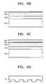
- FIG. 6A through 6Mare cross-sectional views of a method of manufacturing a reflective color filter according to example embodiments.
- spatially relative termse.g., “beneath,” “below,” “lower,” “above,” “upper,” and the like, may be used herein for ease of description to describe one element or feature's relationship to another element(s) or feature(s) as illustrated in the figures. It will be understood that the spatially relative terms are intended to encompass different orientations of the device in use or operation in addition to the orientation depicted in the figures. For example, if the device in the figures is turned over, elements described as “below” or “beneath” other elements or features would then be oriented “above” the other elements or features. Thus, the term “below” may encompass both an orientation of above and below. The device may be otherwise oriented (rotated 90 degrees or at other orientations) and the spatially relative descriptors used herein interpreted accordingly.
- Example embodimentsare described herein with reference to cross-sectional illustrations that are schematic illustrations of idealized embodiments (and intermediate structures) of example embodiments. As such, variations from the shapes of the illustrations as a result, for example, of manufacturing techniques and/or tolerances, are to be expected. Thus, example embodiments should not be construed as limited to the shapes of regions illustrated herein but are to include deviations in shapes that result, for example, from manufacturing. For example, an implanted region illustrated as a rectangle will, typically, have rounded or curved features and/or a gradient of implant concentration at its edges rather than a binary change from implanted to non-implanted region.
- FIG. 1is a perspective view of a photonic crystal optical filter 100 according to example embodiments.
- FIG. 2is a cross-sectional view of the photonic crystal optical filter 100 of FIG. 1 .
- the photonic crystal optical filter 100may include a transparent substrate 130 on which a barrier layer 150 is formed, and a photonic crystal layer 160 formed on the barrier layer 150 .
- An absorption layer 110may be further formed on a lower portion of the transparent substrate 130 .
- the photonic crystal layer 160may be formed to reflect light having a wavelength band corresponding to a photonic band gap according to a periodical distribution of the refractive indices of the photonic crystal layer 160 .
- the photonic crystal layer 160has a structure in which a first material 162 having a relatively high refractive index and a second material 166 having a relatively low refractive index are periodically arranged, and an optical cut-off layer 164 is formed on the first material 162 .
- the first material 162may be formed into island-shaped patterns.
- the island-shaped patterns in FIGS. 1 and 2are rectangular parallelepiped but may also be cylinder-shaped, polygonal pillar-shaped, or otherwise suitably shaped.
- the first material 162has a larger refractive index than the second material 166 .
- a difference between the real parts of the refractive index of the first material 162 and the second material 166may be about 2 or greater.
- a difference between the imaginary parts of the refractive indices of the first material 162 and the second material 166may be about 0.1 or smaller in wavelength bands of visible light.
- the first material 162may be one selected from the group consisting of mono-crystal silicon, poly silicon (poly Si), AlSb, AlAs, AlGaAs, AlGaInP, BP, ZnGeP 2 , and mixtures thereof.
- the second material 166may be one selected from the group consisting of Air, PC, PS, PMMA, Si 3 N 4 , SiO 2 and mixtures thereof.
- the second material 166may be formed as a supporting layer that supports island-shaped patterns of the first material 162 . As illustrated in FIGS. 1 and 2 , the second material 166 may be formed to cover spaces between the patterns of the first material 162 and upper portions of the first material 162 . For example, the above-described structure of the second material 166 may be used to protect patterns of the first material 162 which are formed using amorphous silicon and crystallized to mono-crystal silicon or poly Si.
- the optical cut-off layer 164may improve the cut-off characteristics of the photonic crystal optical filter 100 .
- the optical cut-off layer 164may be formed as a silicon oxide layer (SiO 2 ) or a silicon nitride layer (Si 3 N 4 ).
- the transparent substrate 130is formed to function as a waveguide. Only light having a predetermined wavelength is reflected by the crystalline structure of the photonic crystal layer 160 , and light other than the light having a predetermined wavelength is transmitted and confined in the transparent substrate 130 .
- the transparent substrate 130may be a glass substrate.
- the barrier layer 150may be formed between the transparent substrate 130 and the photonic crystal layer 160 , and has the function of preventing or decreasing reductions in crystalline purity of silicon as impurities inside a glass substrate used as the transparent substrate 130 may migrate into a silicon material used as the first material 162 of the photonic crystal layer 160 during a crystallization process.
- the barrier layer 150may be formed of a material having a similar refractive index to the refractive index of the transparent substrate 130 .
- the barrier layer 150may be formed of a material that is the same as the material that is selected as the second material 166 forming the supporting layer.
- the absorption layer 110may be further formed on a lower portion of the transparent substrate 130 , and may improve reflectivity characteristics of the photonic crystal optical filter 100 by absorbing light confined in the transparent substrate 130 .
- the photonic crystal optical filter 100 having the above-described structuremay reflect light having a predetermined wavelength band using the photonic crystalline structure having a periodical distribution of refractive indices. Because the range and width of the wavelength band are determined by the shape and periods of the patterns of the first material 162 , the wavelength bands of light may be selected with relative ease, and also, the photonic crystal optical filter 100 has an improved filtering performance and thus may be used in various technical fields.
- the photonic crystal optical filter 100may be applied to solar cells, quantum dot light emitting diodes (QD-LED), organic light-emitting diodes (OLED), etc.
- the photonic crystal optical filter 100may be applied as a color filter of a display apparatus.
- FIG. 3is a cross-sectional view of a reflective color filter 200 according to example embodiments.
- the reflective color filter 200may include a transparent substrate 230 , a barrier layer 250 formed on the transparent substrate 230 , and red, green, and blue photonic crystal units 270 , 280 , and 290 , respectively, formed on the barrier layer 250 and reflecting light having a predetermined wavelength band.
- a plurality of pixel areas PA 1 , PA 2 , and PA 3may be formed on the barrier layer 250 .
- the red photonic crystal unit 270 reflecting red color light L R among incident light Lis formed in the pixel area PA 1
- the green photonic crystal unit 280 reflecting green light L G among incident light Lis formed in the pixel area PA 2
- the blue photonic crystal unit 290 reflecting blue light L B among incident light Lis formed in the pixel area PA 3 .
- First materials 272 , 282 , and 292 having a relatively high refractive index and second materials 276 , 286 , and 296 having a relatively low refractive indexare periodically formed in the red photonic crystal unit 270 , the green photonic crystal unit 280 , and the blue photonic crystal unit 290 , respectively, and optical cut-off layer 274 , 284 , and 294 are formed on the first materials 272 , 282 , and 292 , respectively.
- the first materials 272 , 282 , and 292may be formed into island-shaped patterns.
- the materials of the first materials 272 , 282 , and 292 , the second materials 276 , 286 , and 296 , and the optical cut-off layers 274 , 284 , and 294 in the red photonic crystal unit 270 , the green photonic crystal unit 280 , and the blue photonic crystal unit 290may be selected from the various materials used to form the first material 162 , the second material 166 , and the optical cut-off layer 164 of the photonic crystal optical filter 100 .
- the materials of the first materials 272 , 282 , and 292 , the second materials 276 , 286 , and 296 , and the optical cut-off layers 274 , 284 , and 294may be identical or different, and the patterns and periods of the first materials 272 , 282 , and 292 may be selected differently such that each of red photonic crystal unit 270 , green photonic crystal unit 280 and blue photonic crystal unit has photonic band gap corresponding to red, green, and blue colors, respectively.
- the patterns formed with the first material 272 of the red photonic crystal unit 270may have a larger size and period than the patterns of the first material 282 of the green photonic crystal unit 280 or the patterns of the first material 292 of the blue photonic crystal unit 290 .
- the patterns of the first material 282 of the green photonic crystal unit 280may have a larger size and period than the patterns of the first material 292 of the blue photonic crystal unit 290 .
- An absorption layer 210may be further formed on a lower portion of the transparent substrate 230 .
- the absorption layer 210absorbs light confined in the transparent substrate 230 .
- the light of the colors that is not reflected on the red photonic crystal unit 270 , the green photonic crystal unit 280 , and the blue photonic crystal unit 290is confined in the transparent substrate 230 and is absorbed by the absorption layer 210 . Accordingly, color purity of the color filter 200 is increased.
- the red, green, and blue photonic crystal units 270 , 280 , and 290 forming a basic pixelare illustrated.
- the reflective color filter 200substantially has a structure in which the red, green, and blue photonic crystal units 270 , 280 , and 290 are repeatedly arranged.
- a transparent electrode 350is formed on a surface of the transparent substrate 360 facing the liquid crystal layer 330 , and a polarization plate 370 is formed on the other surface of the upper transparent substrate 360 .
- the polarization plate 370may not be used according to the type or the driving mode of the liquid crystal layer 330 , or an additional polarization plate (not shown) (having a polarization axis that is vertical to a polarization axis of the polarization plate 370 or a quarter wavelength plate (not shown) may be further included.
- the display apparatus 300has a structure in which the red, green, and blue photonic crystal units 270 , 280 , and 290 of the reflective color filter 200 and the plurality of TFTs 312 are formed on one substrate, e.g., the transparent substrate 230 . Accordingly, the reflective color filter 200 and the TFT-array layer 310 may be formed in one process.
- the above-described structure of the display apparatus 300may reduce manufacturing errors compared to a conventional liquid crystal display apparatus in which a color filter is formed on an upper substrate and a TFT array is formed on a lower substrate. For example, in a conventional liquid crystal display where the color filter and the TFT array are separately manufactured and coupled to each other, coupling in alignment based on units of pixels is required. Thus, alignment errors may occur. However, because the color filter 200 and the TFT array layer 310 according to example embodiments may be formed on one substrate, such errors may be reduced.
- the plurality of TFTs 312 and the red, green, and blue photonic crystal units 270 , 280 , and 290may be formed on one substrate, although example embodiments are not limited thereto.
- the reflective color filter 200 and the TFT-array layer 310may be formed as separate layers.
- a barrier layer 450 and a silicon layer 462 corresponding to the first materialmay be sequentially formed on a transparent substrate 430 .
- the transparent substrate 430may be a glass substrate.
- the silicon layer 462may be used because silicon has a relatively large refractive index in its real part and a relatively small refractive index in its imaginary part. Such characteristics are more evident in the case of mono-crystal silicon or poly silicon (poly Si).
- the silicon layer 462may be formed of amorphous silicon, and in such a case, the silicon layer 462 may undergo a recrystallization process, as will be described later.
- the barrier layer 450may be formed of various suitable materials, e.g., poly carbonate (PC), poly styrene (PS), poly methyl methacrylate (PMMA), Si 3 N 4 , SiO 2 , etc., or a material that has a refractive index having a small difference from that of the transparent substrate 430 .
- PCpoly carbonate
- PSpoly styrene
- PMMApoly methyl methacrylate
- Si 3 N 4SiO 2
- SiO 2SiO 2
- a hard mask layer 464may be formed on the silicon layer 462 .
- the hard mask layer 464functions as a hard mask for etching, and also provides etching selectivity.
- the hard mask layer 464may be formed as a silicon oxide layer (SiO 2 ) or a silicon nitride layer (Si 3 N 4 ). A portion of the hard mask layer 464 remains after the silicon layer 462 is patterned and improves the cut-off characteristics of the manufactured reflective color filter 400 , because the silicon oxide layer (SiO 2 ) or the silicon nitride layer (Si 3 N 4 ) has a lower refractive index than a silicon layer 462 .
- a resin layer 465 ′may be formed on the hard mask layer 464 for the subsequent formation of a resist pattern.
- a suitable material for the resin layer 465 ′may include a UV curing resin.
- a mold Mmay be prepared.
- the mold Mmay be prepared for a nano-imprinting process, and a detailed pattern of the mold M may be formed to correspond to the island-shaped patterns which are to be formed from the silicon layer 462 .
- the mold. Mmay have one of the arrangements among the pixel arrays described with reference to FIGS. 4A through 4C , and may have different patterns and periods respectively corresponding to colors.
- the resist pattern 465may be used as a mask to etch the hard mask layer 464 and expose the silicon layer 462 .
- the resist pattern 465 and the hard mask layer 464may be used as a mask to etch the silicon layer 462 and expose the barrier layer 450 . Accordingly, the silicon layer 462 may be formed as island-shaped patterns.
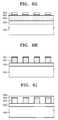
- a scanning direction during EL irradiationmay be parallel to an arrangement direction of patterns of the silicon layer 462 (flat leading end method).
- a scanning directionmay be at about 45° to the arrangement direction of the patterns of the silicon layer 462 (tapered leading end method).
- the silicon layer 462 which is formed of amorphous siliconmay be crystallized by the EL irradiation to a crystalline silicon layer 463 .
- one nucleusmay be formed at each of the corners of the crystalline silicon layer 463 , and thus crystallization may be performed with greater ease.
- the reflection wavelengths bands of a photonic crystal optical filter according to example embodimentsmay be determined with relative ease based on the shape and periods of relatively highly refractive patterns, and the photonic crystal optical filter may have improved filtering performance.
- the reflective color filter according to example embodimentshas beneficial color properties and may realize R, G, and B colors using one nano-imprinting process unlike a conventional photolithography process which needs to be performed three times to realize R, G, and B colors, thereby reducing the number of manufacturing processes.
- the display apparatus according to example embodimentshas improved quality, and a reflective color filter and a TFT array may be formed on one substrate, thereby reducing the number of manufacturing processes, the manufacturing errors, and manufacturing costs.
Landscapes
- Physics & Mathematics (AREA)
- General Physics & Mathematics (AREA)
- Optics & Photonics (AREA)
- Optical Filters (AREA)
Abstract
Description
Claims (28)
Applications Claiming Priority (4)
| Application Number | Priority Date | Filing Date | Title |
|---|---|---|---|
| KR20080099774 | 2008-10-10 | ||
| KR10-2008-0099774 | 2008-10-10 | ||
| KR10-2009-0011215 | 2009-02-11 | ||
| KR1020090011215AKR101557800B1 (en) | 2008-10-10 | 2009-02-11 | Photonic crystal optical filter, reflection type color filter using the same, and display device |
Publications (2)
| Publication Number | Publication Date |
|---|---|
| US20100091224A1 US20100091224A1 (en) | 2010-04-15 |
| US8264637B2true US8264637B2 (en) | 2012-09-11 |
Family
ID=42098542
Family Applications (1)
| Application Number | Title | Priority Date | Filing Date |
|---|---|---|---|
| US12/461,455Active2030-06-27US8264637B2 (en) | 2008-10-10 | 2009-08-12 | Photonic crystal optical filter, reflective color filter, display apparatus using the reflective color filter, and method of manufacturing the reflective color filter |
Country Status (1)
| Country | Link |
|---|---|
| US (1) | US8264637B2 (en) |
Cited By (11)
| Publication number | Priority date | Publication date | Assignee | Title |
|---|---|---|---|---|
| US9478713B2 (en) | 2014-05-27 | 2016-10-25 | Rohm And Haas Electronic Materials Llc | Nanostructure material methods and devices |
| US10649113B2 (en) | 2017-09-29 | 2020-05-12 | Nike, Inc. | Structurally-colored articles and methods for making and using structurally-colored articles |
| US11129444B1 (en) | 2020-08-07 | 2021-09-28 | Nike, Inc. | Footwear article having repurposed material with concealing layer |
| US11241062B1 (en) | 2020-08-07 | 2022-02-08 | Nike, Inc. | Footwear article having repurposed material with structural-color concealing layer |
| US11597996B2 (en) | 2019-06-26 | 2023-03-07 | Nike, Inc. | Structurally-colored articles and methods for making and using structurally-colored articles |
| US11612208B2 (en) | 2019-07-26 | 2023-03-28 | Nike, Inc. | Structurally-colored articles and methods for making and using structurally-colored articles |
| US11889894B2 (en) | 2020-08-07 | 2024-02-06 | Nike, Inc. | Footwear article having concealing layer |
| US11987074B2 (en) | 2020-05-29 | 2024-05-21 | Nike, Inc. | Structurally-colored articles having layers which taper in thickness |
| US11986042B2 (en) | 2019-10-21 | 2024-05-21 | Nike, Inc. | Structurally-colored articles and methods for making and using structurally-colored articles |
| US12409243B2 (en) | 2017-02-14 | 2025-09-09 | Nike, Inc. | Anti-odor compositions, structures having anti-odor characteristics, methods of making the anti-odor compositions and the structures |
| US12442955B2 (en) | 2022-11-29 | 2025-10-14 | Nike, Inc. | Structurally-colored articles and methods for making and using structurally-colored articles |
Families Citing this family (42)
| Publication number | Priority date | Publication date | Assignee | Title |
|---|---|---|---|---|
| KR101649696B1 (en)* | 2009-10-29 | 2016-08-22 | 엘지디스플레이 주식회사 | Fringe field switching liquid crystal display device and method of fabricating the same |
| KR20110083361A (en)* | 2010-01-14 | 2011-07-20 | 삼성전자주식회사 | Reflective color filter and display device including same |
| KR20110086363A (en)* | 2010-01-22 | 2011-07-28 | 삼성전자주식회사 | Thin films with nanostructures, surface light sources and display devices employing them |
| WO2012087269A1 (en)* | 2010-12-20 | 2012-06-28 | Hewlett-Packard Development Company, L.P. | Reflective display utilizing luminescence |
| CN102157643B (en)* | 2011-04-08 | 2012-09-26 | 华中科技大学 | Method for preparing GaN-based photonic crystal LED based on nanoimprint lithography |
| GB201117480D0 (en) | 2011-10-10 | 2011-11-23 | Palikaras George | Filter |
| CN102508375A (en)* | 2011-11-09 | 2012-06-20 | 南开大学 | Terahertz tunable filter of metal photonic crystal |
| EP2979133A4 (en) | 2013-03-26 | 2016-11-16 | Clearink Displays Inc | Displaced porous electrode for frustrating tir |
| CN103226259B (en)* | 2013-04-09 | 2015-07-01 | 北京京东方光电科技有限公司 | Liquid crystal display panel, display device, and manufacturing method of liquid crystal display panel |
| US9280029B2 (en) | 2013-05-13 | 2016-03-08 | Clearink Displays, Inc. | Registered reflective element for a brightness enhanced TIR display |
| EP2999989A4 (en) | 2013-05-22 | 2017-01-04 | Clearink Displays, Inc. | Method and apparatus for improved color filter saturation |
| EP3019911A4 (en) | 2013-07-08 | 2017-06-28 | Clearink Displays, Inc. | Tir-modulated wide viewing angle display |
| US10705404B2 (en) | 2013-07-08 | 2020-07-07 | Concord (Hk) International Education Limited | TIR-modulated wide viewing angle display |
| US9740075B2 (en) | 2013-09-10 | 2017-08-22 | Clearink Displays, Inc. | Method and system for perforated reflective film display device |
| JP6272621B2 (en) | 2013-09-30 | 2018-01-31 | クリアインク ディスプレイズ, インコーポレイテッドClearink Displays, Inc. | Method and apparatus for front illuminated semi-retroreflective display |
| CN104201188B (en)* | 2014-08-22 | 2017-07-25 | 京东方科技集团股份有限公司 | OLED pixel unit and its preparation method, display panel and display device |
| US9897890B2 (en) | 2014-10-07 | 2018-02-20 | Clearink Displays, Inc. | Reflective image display with threshold |
| CN107111016B (en) | 2014-10-08 | 2020-08-28 | 协和(香港)国际教育有限公司 | Color filter aligned reflective display |
| EP3224672A4 (en)* | 2014-11-24 | 2018-06-27 | Clearink Displays, Inc. | Dispersive periodic concentrator |
| US10386691B2 (en) | 2015-06-24 | 2019-08-20 | CLEARink Display, Inc. | Method and apparatus for a dry particle totally internally reflective image display |
| CN105044974B (en)* | 2015-08-28 | 2017-08-29 | 京东方科技集团股份有限公司 | Chromatic filter layer, display base plate and display device |
| US10261221B2 (en) | 2015-12-06 | 2019-04-16 | Clearink Displays, Inc. | Corner reflector reflective image display |
| US10386547B2 (en) | 2015-12-06 | 2019-08-20 | Clearink Displays, Inc. | Textured high refractive index surface for reflective image displays |
| CN105353556B (en)* | 2015-12-09 | 2017-12-29 | 深圳市华星光电技术有限公司 | Display device |
| US10489924B2 (en)* | 2016-03-30 | 2019-11-26 | Samsung Electronics Co., Ltd. | Structured light generator and object recognition apparatus including the same |
| CN106681046B (en)* | 2016-11-21 | 2020-03-17 | 京东方科技集团股份有限公司 | Color film substrate and display device |
| KR102587958B1 (en)* | 2017-02-03 | 2023-10-11 | 삼성전자주식회사 | Meta optical device and method of fabricating the same |
| CN106838849B (en) | 2017-02-23 | 2019-11-26 | 京东方科技集团股份有限公司 | Collimated light source component, display device and the method for manufacturing collimated light source component |
| CN106707626B (en)* | 2017-02-24 | 2019-11-15 | 深圳市华星光电半导体显示技术有限公司 | Liquid crystal display panel and liquid crystal display device |
| EP3676973A4 (en) | 2017-08-31 | 2021-05-05 | Metalenz, Inc. | TRANSMISSIVE METASURFACE LENS INTEGRATION |
| US11156753B2 (en) | 2017-12-18 | 2021-10-26 | Viavi Solutions Inc. | Optical filters |
| CN108594345B (en) | 2018-04-26 | 2021-09-24 | 京东方科技集团股份有限公司 | A photonic crystal, QLED device, display panel, glasses |
| EP3617757B1 (en)* | 2018-08-27 | 2021-02-24 | CSEM Centre Suisse d'Electronique et de Microtechnique SA - Recherche et Développement | Optical filter, optical filter system, spectrometer and method of fabrication thereof |
| US11784282B2 (en)* | 2018-10-26 | 2023-10-10 | Samsung Electronics Co., Ltd. | Quantum dot display device |
| CN114286953B (en) | 2019-07-26 | 2025-04-01 | 梅特兰兹股份有限公司 | Porosity-metasurface and hybrid refraction-metasurface imaging systems |
| KR102637109B1 (en)* | 2019-09-24 | 2024-02-15 | 삼성전자주식회사 | Optical thin film for metasurface and meta optical device including the same |
| FR3105748B1 (en)* | 2019-12-26 | 2022-09-02 | Aledia | Device for laser treatment and laser treatment method |
| CN111524946A (en)* | 2020-04-27 | 2020-08-11 | 武汉华星光电半导体显示技术有限公司 | OLED display panel, preparation method and display device |
| KR102801337B1 (en) | 2020-10-31 | 2025-04-30 | 후아웨이 테크놀러지 컴퍼니 리미티드 | Reflective display devices, display panels and display screens |
| CN116940866A (en)* | 2021-01-06 | 2023-10-24 | 梅特兰兹股份有限公司 | Self-aligned nanopillar coatings and methods of making the same |
| CN113138490A (en)* | 2021-04-23 | 2021-07-20 | 武汉华星光电技术有限公司 | Reflective display panel |
| CN120188073A (en) | 2022-03-31 | 2025-06-20 | 梅特兰兹股份有限公司 | Polarization-sorting metasurface microlens array device |
Citations (11)
| Publication number | Priority date | Publication date | Assignee | Title |
|---|---|---|---|---|
| US5998298A (en)* | 1998-04-28 | 1999-12-07 | Sandia Corporation | Use of chemical-mechanical polishing for fabricating photonic bandgap structures |
| US6064511A (en)* | 1998-03-31 | 2000-05-16 | The Research Foundation Of State University Of New York | Fabrication methods and structured materials for photonic devices |
| US20010026668A1 (en)* | 2000-03-29 | 2001-10-04 | Nec Corporation | Photonic crystal waveguide and directional coupler using the same |
| US20030025863A1 (en)* | 2001-07-27 | 2003-02-06 | Seiko Epson Corporation | Liquid crystal display device and electronic device |
| US20040264903A1 (en)* | 2001-10-19 | 2004-12-30 | Dridi Kim Hakim | Intergrated photonic crystal structure and method of producing same |
| US20050238310A1 (en)* | 2004-04-12 | 2005-10-27 | Canon Kabushiki Kaisha | Stacked three dimensional photonic crystal, light emitting device, and image display apparatus |
| US20060159411A1 (en)* | 2004-05-27 | 2006-07-20 | Miller Robert A | Photonic integrated circuit |
| US20070002438A1 (en)* | 2001-12-13 | 2007-01-04 | Sony Corporation | Screen, its manufacturing method and image display system |
| US7421179B1 (en)* | 2006-09-29 | 2008-09-02 | Wei Jiang | Apparatus and method for switching, modulation and dynamic control of light transmission using photonic crystals |
| US20090116029A1 (en)* | 2005-09-06 | 2009-05-07 | Yasuo Ohtera | Wavelength division image measuring device |
| US20100014821A1 (en)* | 2007-01-10 | 2010-01-21 | Masatoshi Tokushima | Optical control device |
- 2009
- 2009-08-12USUS12/461,455patent/US8264637B2/enactiveActive
Patent Citations (15)
| Publication number | Priority date | Publication date | Assignee | Title |
|---|---|---|---|---|
| US6064511A (en)* | 1998-03-31 | 2000-05-16 | The Research Foundation Of State University Of New York | Fabrication methods and structured materials for photonic devices |
| US5998298A (en)* | 1998-04-28 | 1999-12-07 | Sandia Corporation | Use of chemical-mechanical polishing for fabricating photonic bandgap structures |
| US20010026668A1 (en)* | 2000-03-29 | 2001-10-04 | Nec Corporation | Photonic crystal waveguide and directional coupler using the same |
| US6631236B2 (en)* | 2000-03-29 | 2003-10-07 | Nec Corporation | Photonic crystal waveguide and directional coupler using the same |
| US20030025863A1 (en)* | 2001-07-27 | 2003-02-06 | Seiko Epson Corporation | Liquid crystal display device and electronic device |
| US7194174B2 (en)* | 2001-10-19 | 2007-03-20 | Ignis Technologies As | Integrated photonic crystal structure and method of producing same |
| US20040264903A1 (en)* | 2001-10-19 | 2004-12-30 | Dridi Kim Hakim | Intergrated photonic crystal structure and method of producing same |
| US20070002438A1 (en)* | 2001-12-13 | 2007-01-04 | Sony Corporation | Screen, its manufacturing method and image display system |
| US7345818B2 (en)* | 2001-12-13 | 2008-03-18 | Sony Corporation | Screen, its manufacturing method and image display system |
| US20050238310A1 (en)* | 2004-04-12 | 2005-10-27 | Canon Kabushiki Kaisha | Stacked three dimensional photonic crystal, light emitting device, and image display apparatus |
| US20060159411A1 (en)* | 2004-05-27 | 2006-07-20 | Miller Robert A | Photonic integrated circuit |
| US7447404B2 (en)* | 2004-05-27 | 2008-11-04 | Energy Conversion Devices, Inc. | Photonic integrated circuit |
| US20090116029A1 (en)* | 2005-09-06 | 2009-05-07 | Yasuo Ohtera | Wavelength division image measuring device |
| US7421179B1 (en)* | 2006-09-29 | 2008-09-02 | Wei Jiang | Apparatus and method for switching, modulation and dynamic control of light transmission using photonic crystals |
| US20100014821A1 (en)* | 2007-01-10 | 2010-01-21 | Masatoshi Tokushima | Optical control device |
Cited By (34)
| Publication number | Priority date | Publication date | Assignee | Title |
|---|---|---|---|---|
| US9478713B2 (en) | 2014-05-27 | 2016-10-25 | Rohm And Haas Electronic Materials Llc | Nanostructure material methods and devices |
| US12409243B2 (en) | 2017-02-14 | 2025-09-09 | Nike, Inc. | Anti-odor compositions, structures having anti-odor characteristics, methods of making the anti-odor compositions and the structures |
| US11385382B2 (en) | 2017-09-29 | 2022-07-12 | Nike, Inc. | Structurally-colored articles and methods for making and using structurally-colored articles |
| US11391867B2 (en) | 2017-09-29 | 2022-07-19 | Nike, Inc. | Structurally-colored articles and methods for making and using structurally-colored articles |
| US10928552B2 (en) | 2017-09-29 | 2021-02-23 | Nike, Inc. | Structurally-colored articles and methods for making and using structurally-colored articles |
| US10955588B2 (en) | 2017-09-29 | 2021-03-23 | Nike, Inc. | Structurally-colored articles and methods for making and using structurally-colored articles |
| US11112537B2 (en) | 2017-09-29 | 2021-09-07 | Nike, Inc. | Structurally-colored articles and methods for making and using structurally-colored articles |
| US10732322B2 (en) | 2017-09-29 | 2020-08-04 | Nike, Inc. | Structurally-colored articles and methods for making and using structurally-colored articles |
| US11131791B2 (en) | 2017-09-29 | 2021-09-28 | Nike, Inc. | Structurally-colored articles and methods for making and using structurally-colored articles |
| US12360288B2 (en) | 2017-09-29 | 2025-07-15 | Nike, Inc. | Structurally-colored articles and methods of making and using structurally-colored articles |
| US10649113B2 (en) | 2017-09-29 | 2020-05-12 | Nike, Inc. | Structurally-colored articles and methods for making and using structurally-colored articles |
| US10928553B2 (en) | 2017-09-29 | 2021-02-23 | Nike, Inc. | Structurally-colored articles and methods for making and using structurally-colored articles |
| US11397283B2 (en) | 2017-09-29 | 2022-07-26 | Nike, Inc. | Structurally-colored articles and methods for making and using structurally-colored articles |
| US11402546B2 (en) | 2017-09-29 | 2022-08-02 | Nike, Inc. | Structurally-colored articles and methods for making and using structurally-colored articles |
| US11402545B2 (en) | 2017-09-29 | 2022-08-02 | Nike, Inc. | Structurally-colored articles and methods for making and using structurally-colored articles |
| US11402544B2 (en) | 2017-09-29 | 2022-08-02 | Nike, Inc. | Structurally-colored articles and methods for making and using structurally-colored articles |
| US12000977B2 (en) | 2017-09-29 | 2024-06-04 | Nike, Inc. | Structurally-colored articles and methods for making and using structurally-colored articles |
| US11994649B2 (en) | 2017-09-29 | 2024-05-28 | Nike, Inc. | Structurally-colored articles and methods for making and using structurally-colored articles |
| US11609359B2 (en) | 2017-09-29 | 2023-03-21 | Nike, Inc. | Structurally-colored articles and methods for making and using structurally-colored articles |
| US11614563B2 (en) | 2017-09-29 | 2023-03-28 | Nike, Inc. | Structurally-colored articles and methods for making and using structurally-colored articles |
| US11987873B2 (en) | 2019-06-26 | 2024-05-21 | Nike, Inc. | Structurally-colored articles and methods for making and using structurally-colored articles |
| US11840755B2 (en) | 2019-06-26 | 2023-12-12 | Nike, Inc. | Structurally-colored articles and methods for making and using structurally-colored articles |
| US11597996B2 (en) | 2019-06-26 | 2023-03-07 | Nike, Inc. | Structurally-colored articles and methods for making and using structurally-colored articles |
| US11612208B2 (en) | 2019-07-26 | 2023-03-28 | Nike, Inc. | Structurally-colored articles and methods for making and using structurally-colored articles |
| US11986042B2 (en) | 2019-10-21 | 2024-05-21 | Nike, Inc. | Structurally-colored articles and methods for making and using structurally-colored articles |
| US11987074B2 (en) | 2020-05-29 | 2024-05-21 | Nike, Inc. | Structurally-colored articles having layers which taper in thickness |
| US11987073B2 (en) | 2020-05-29 | 2024-05-21 | Nike, Inc. | Structurally-colored articles having layers which taper in thickness |
| US11889894B2 (en) | 2020-08-07 | 2024-02-06 | Nike, Inc. | Footwear article having concealing layer |
| US11412817B2 (en) | 2020-08-07 | 2022-08-16 | Nike, Inc. | Footwear article having repurposed material with concealing layer |
| US12150512B2 (en) | 2020-08-07 | 2024-11-26 | Nike, Inc. | Footwear article having repurposed material with structural-color concealing layer |
| US12167771B2 (en) | 2020-08-07 | 2024-12-17 | Nike, Inc. | Footwear article having repurposed material with concealing layer |
| US11241062B1 (en) | 2020-08-07 | 2022-02-08 | Nike, Inc. | Footwear article having repurposed material with structural-color concealing layer |
| US11129444B1 (en) | 2020-08-07 | 2021-09-28 | Nike, Inc. | Footwear article having repurposed material with concealing layer |
| US12442955B2 (en) | 2022-11-29 | 2025-10-14 | Nike, Inc. | Structurally-colored articles and methods for making and using structurally-colored articles |
Also Published As
| Publication number | Publication date |
|---|---|
| US20100091224A1 (en) | 2010-04-15 |
Similar Documents
| Publication | Publication Date | Title |
|---|---|---|
| US8264637B2 (en) | Photonic crystal optical filter, reflective color filter, display apparatus using the reflective color filter, and method of manufacturing the reflective color filter | |
| US8363185B2 (en) | Photonic crystal optical filter, transmissive color filter, transflective color filter, and display apparatus using the color filters | |
| US9019590B2 (en) | Spatial light modulator with integrated optical compensation structure | |
| TWI779020B (en) | Display apparatus | |
| US20090284696A1 (en) | Photonic crystal type color filter and reflective liquid crystal display device having the same | |
| US9703191B2 (en) | Method of manufacturing color conversion substrate | |
| US20140118656A1 (en) | Liquid crystal display and manufacturing method thereof | |
| KR101557800B1 (en) | Photonic crystal optical filter, reflection type color filter using the same, and display device | |
| KR20070010472A (en) | Hybrid polarizer, manufacturing method thereof and display device having same | |
| JP5692909B2 (en) | Reflective color filter and display device including the same | |
| US20090185120A1 (en) | Thin film transistor substrate and method for manufacturing the same | |
| JP2008191668A (en) | Photoresist forming method and display panel manufacturing method | |
| US20210041730A1 (en) | Display panel, manufacturing method thereof and display device | |
| KR102344911B1 (en) | Photoluminescence device, method of manufacturing the same and display apparatus having the same | |
| KR20110075537A (en) | Manufacturing Method of Color Filter and Liquid Crystal Display Using Surface Plasmon | |
| KR20040056666A (en) | method of fabricating of color filter panel for liquid crystal display | |
| KR20100040650A (en) | Photonic crystal type optical filter, reflective type color filter, transflective type color filter and display device using the same | |
| KR20100121943A (en) | Method of fabricatinf photonic crystal type color filter | |
| US7588866B2 (en) | Filter arrays for liquid crystal displays and methods of making the same | |
| US9019446B2 (en) | Liquid crystal display device and manufacturing method thereof | |
| WO2007077644A1 (en) | Liquid crystal display device | |
| TW201831930A (en) | Polarizing plate, manufacturing method of polarizing plate, and display device comprising a linear portion, and a plurality of linear regions for preventing light leakage | |
| US20070178390A1 (en) | Exposure mask, liquid crystal display device using the same, and method of manufacturing liquid crystal display device using the same | |
| RU2379725C2 (en) | Spatial light modulator with integrated optical compensation structure | |
| JP4393186B2 (en) | Photomask and method for producing pattern formed body using the same |
Legal Events
| Date | Code | Title | Description |
|---|---|---|---|
| AS | Assignment | Owner name:SAMSUNG ELECTRONICS CO., LTD.,KOREA, REPUBLIC OF Free format text:ASSIGNMENT OF ASSIGNORS INTEREST;ASSIGNORS:CHO, EUN-HYOUNG;SOHN, JIN-SEUNG;KANG, SEOCK-HWAN;AND OTHERS;REEL/FRAME:023127/0659 Effective date:20090723 Owner name:SAMSUNG ELECTRONICS CO., LTD., KOREA, REPUBLIC OF Free format text:ASSIGNMENT OF ASSIGNORS INTEREST;ASSIGNORS:CHO, EUN-HYOUNG;SOHN, JIN-SEUNG;KANG, SEOCK-HWAN;AND OTHERS;REEL/FRAME:023127/0659 Effective date:20090723 | |
| STCF | Information on status: patent grant | Free format text:PATENTED CASE | |
| FPAY | Fee payment | Year of fee payment:4 | |
| MAFP | Maintenance fee payment | Free format text:PAYMENT OF MAINTENANCE FEE, 8TH YEAR, LARGE ENTITY (ORIGINAL EVENT CODE: M1552); ENTITY STATUS OF PATENT OWNER: LARGE ENTITY Year of fee payment:8 | |
| MAFP | Maintenance fee payment | Free format text:PAYMENT OF MAINTENANCE FEE, 12TH YEAR, LARGE ENTITY (ORIGINAL EVENT CODE: M1553); ENTITY STATUS OF PATENT OWNER: LARGE ENTITY Year of fee payment:12 |