US8264357B2 - Wireless IC device - Google Patents
Wireless IC deviceDownload PDFInfo
- Publication number
- US8264357B2 US8264357B2US12/429,346US42934609AUS8264357B2US 8264357 B2US8264357 B2US 8264357B2US 42934609 AUS42934609 AUS 42934609AUS 8264357 B2US8264357 B2US 8264357B2
- Authority
- US
- United States
- Prior art keywords
- coupler
- wireless
- mount
- feeder circuit
- circuit board
- Prior art date
- Legal status (The legal status is an assumption and is not a legal conclusion. Google has not performed a legal analysis and makes no representation as to the accuracy of the status listed.)
- Active
Links
Images


Classifications
- H—ELECTRICITY
- H01—ELECTRIC ELEMENTS
- H01Q—ANTENNAS, i.e. RADIO AERIALS
- H01Q9/00—Electrically-short antennas having dimensions not more than twice the operating wavelength and consisting of conductive active radiating elements
- H01Q9/04—Resonant antennas
- H01Q9/16—Resonant antennas with feed intermediate between the extremities of the antenna, e.g. centre-fed dipole
- G—PHYSICS
- G06—COMPUTING OR CALCULATING; COUNTING
- G06K—GRAPHICAL DATA READING; PRESENTATION OF DATA; RECORD CARRIERS; HANDLING RECORD CARRIERS
- G06K19/00—Record carriers for use with machines and with at least a part designed to carry digital markings
- G06K19/06—Record carriers for use with machines and with at least a part designed to carry digital markings characterised by the kind of the digital marking, e.g. shape, nature, code
- G06K19/067—Record carriers with conductive marks, printed circuits or semiconductor circuit elements, e.g. credit or identity cards also with resonating or responding marks without active components
- G06K19/07—Record carriers with conductive marks, printed circuits or semiconductor circuit elements, e.g. credit or identity cards also with resonating or responding marks without active components with integrated circuit chips
- G06K19/077—Constructional details, e.g. mounting of circuits in the carrier
- G06K19/07749—Constructional details, e.g. mounting of circuits in the carrier the record carrier being capable of non-contact communication, e.g. constructional details of the antenna of a non-contact smart card
- G—PHYSICS
- G06—COMPUTING OR CALCULATING; COUNTING
- G06K—GRAPHICAL DATA READING; PRESENTATION OF DATA; RECORD CARRIERS; HANDLING RECORD CARRIERS
- G06K19/00—Record carriers for use with machines and with at least a part designed to carry digital markings
- G06K19/06—Record carriers for use with machines and with at least a part designed to carry digital markings characterised by the kind of the digital marking, e.g. shape, nature, code
- G06K19/067—Record carriers with conductive marks, printed circuits or semiconductor circuit elements, e.g. credit or identity cards also with resonating or responding marks without active components
- G06K19/07—Record carriers with conductive marks, printed circuits or semiconductor circuit elements, e.g. credit or identity cards also with resonating or responding marks without active components with integrated circuit chips
- G06K19/077—Constructional details, e.g. mounting of circuits in the carrier
- G06K19/07749—Constructional details, e.g. mounting of circuits in the carrier the record carrier being capable of non-contact communication, e.g. constructional details of the antenna of a non-contact smart card
- G06K19/0775—Constructional details, e.g. mounting of circuits in the carrier the record carrier being capable of non-contact communication, e.g. constructional details of the antenna of a non-contact smart card arrangements for connecting the integrated circuit to the antenna
- G06K19/07756—Constructional details, e.g. mounting of circuits in the carrier the record carrier being capable of non-contact communication, e.g. constructional details of the antenna of a non-contact smart card arrangements for connecting the integrated circuit to the antenna the connection being non-galvanic, e.g. capacitive
- H—ELECTRICITY
- H01—ELECTRIC ELEMENTS
- H01Q—ANTENNAS, i.e. RADIO AERIALS
- H01Q1/00—Details of, or arrangements associated with, antennas
- H01Q1/12—Supports; Mounting means
- H01Q1/22—Supports; Mounting means by structural association with other equipment or articles
- H01Q1/2208—Supports; Mounting means by structural association with other equipment or articles associated with components used in interrogation type services, i.e. in systems for information exchange between an interrogator/reader and a tag/transponder, e.g. in Radio Frequency Identification [RFID] systems
- H01Q1/2225—Supports; Mounting means by structural association with other equipment or articles associated with components used in interrogation type services, i.e. in systems for information exchange between an interrogator/reader and a tag/transponder, e.g. in Radio Frequency Identification [RFID] systems used in active tags, i.e. provided with its own power source or in passive tags, i.e. deriving power from RF signal
- H—ELECTRICITY
- H01—ELECTRIC ELEMENTS
- H01Q—ANTENNAS, i.e. RADIO AERIALS
- H01Q1/00—Details of, or arrangements associated with, antennas
- H01Q1/12—Supports; Mounting means
- H01Q1/22—Supports; Mounting means by structural association with other equipment or articles
- H01Q1/24—Supports; Mounting means by structural association with other equipment or articles with receiving set
- H—ELECTRICITY
- H01—ELECTRIC ELEMENTS
- H01Q—ANTENNAS, i.e. RADIO AERIALS
- H01Q1/00—Details of, or arrangements associated with, antennas
- H01Q1/36—Structural form of radiating elements, e.g. cone, spiral, umbrella; Particular materials used therewith
- H01Q1/38—Structural form of radiating elements, e.g. cone, spiral, umbrella; Particular materials used therewith formed by a conductive layer on an insulating support
- H—ELECTRICITY
- H01—ELECTRIC ELEMENTS
- H01Q—ANTENNAS, i.e. RADIO AERIALS
- H01Q7/00—Loop antennas with a substantially uniform current distribution around the loop and having a directional radiation pattern in a plane perpendicular to the plane of the loop
- H—ELECTRICITY
- H01—ELECTRIC ELEMENTS
- H01Q—ANTENNAS, i.e. RADIO AERIALS
- H01Q9/00—Electrically-short antennas having dimensions not more than twice the operating wavelength and consisting of conductive active radiating elements
- H01Q9/04—Resonant antennas
- H01Q9/16—Resonant antennas with feed intermediate between the extremities of the antenna, e.g. centre-fed dipole
- H01Q9/28—Conical, cylindrical, cage, strip, gauze, or like elements having an extended radiating surface; Elements comprising two conical surfaces having collinear axes and adjacent apices and fed by two-conductor transmission lines
Definitions
- the present inventionrelates to wireless IC devices and, in particular, to a wireless IC device including a wireless IC chip for use in an RFID (Radio Frequency Identification) system.
- RFIDRadio Frequency Identification
- RFID systems for transmitting informationhave recently been developed as a management system of goods.
- a reader/writer generating an induction electromagnetic fieldcommunicates in a contactless fashion with an IC chip (also referred to as an IC tag or a wireless IC chip) storing predetermined information attached to goods or a container.
- an IC chipalso referred to as an IC tag or a wireless IC chip
- a wireless tag known as a wireless IC deviceincludes an IC chip mounted thereon.
- the wireless tagincludes a dipole antenna (including a pair of main antenna elements and a matching unit) on a piezoelectric substrate and a tag IC electrically connected to ends of the dipole antenna.
- the matching unitarranged between the tag IC and the main antenna elements, has a function of matching impedances between the tag IC and the main antenna elements.
- the wireless taghas a problem discussed below.
- a connection terminal of a small tag ICneeds to be accurately positioned with respect to the dipole antenna and then mounted.
- a high precision mounting apparatusis thus required to avoid connection failures.
- Matching unitseach occupying a large area, need to be arranged for the pair of main antenna elements in a manner such that the matching units do not overlap the antennas.
- the size of the wireless tagmay be increased.
- preferred embodiments of the present inventionprovide a miniaturized wireless IC device without the need for high precision mounting and that is appropriate for use in an RFID system.
- a wireless IC deviceincludes a wireless IC chip having input and output terminals arranged to process transmission and reception signals, a feeder circuit board including a feeder circuit, the feeder circuit including at least one of a resonator circuit and a matching circuit, the feeder circuit including a first coupler and a second coupler, each coupler including an inductance element, and a first radiation plate including a first mount having the feeder circuit board mounted thereon, and a second radiation plate including a second mount having the feeder circuit board mounted thereon, each radiation plate being made of a metal.
- An electromagnetic coupler module having the feeder circuit board and the wireless IC chip mounted on the feeder circuit boardis arranged with the input and output terminals of the wireless IC chip electrically connected to the feeder circuit.
- the first coupleris electromagnetically coupled with the first mount and the second coupler is electromagnetically mounted with the second mount.
- the wireless IC chipis operated by the first and second couplers in response to a signal received by the first and second radiation plates, and a response signal from the wireless IC chip is radiated to the outside from the first and second radiation plates via the first and second couplers.
- the first and second radiation platesinclude the first and second mounts arranged to mount the feeder circuit board thereon.
- the feeder circuit including the first and second couplers electromagnetically coupled with the first and second mountsperforms impedance matching between the wireless IC chip and the first and second radiation plate and/or sets a resonance frequency of a signal.
- the wireless IC chipis not connected to the large radiation plate, but is electrically connected to and mounted on the small feeder circuit board. Thus, the mounting of the wireless IC chip is facilitated.
- the feeder circuitis not directly electrically connected to the first and second radiation plates, and the first and second couplers are electromagnetically coupled with the first and second mounts. The accuracy level required when the feeder circuit board is mounted on the radiation plate is reduced. Since a single feeder circuit is used, the feeder circuit board can be miniaturized. Since the feeder circuit is not directly connected to the radiation plate, the wireless IC chip is prevented from being broken even if an electrostatic charge enters via the radiation plate.
- An operating frequency of the wireless IC chipis determined by the feeder circuit (resonator circuit) arranged on the feeder circuit board, and does not depend on the length and size of the first and second mounts where the first and second radiation plates are coupled with the feeder circuit (resonator circuit). Operation error does not occur even if the mounting position of the feeder circuit board with respect to the first and second radiation plates is deviated to some degree on the feeder circuit board. The required mounting accuracy is thus reduced.
- the wireless IC chipmay have an information rewritable function in addition to the function of storing a variety of information related to the goods to which the wireless IC device is attached, and further may have an information processing function other than the function of the RFID system.
- the electromagnetic coupler moduleis constructed by arranging the feeder circuit, including the first coupler and the second coupler, on the feeder circuit board, and mounting the wireless IC chip on the feeder circuit board.
- the first and second couplersare thus electromagnetically coupled with the first and second mounts on the first and second radiation plates. This arrangement eliminates the need for mounting the wireless IC chip and the feeder circuit board with high accuracy, and the wireless IC device can be miniaturized.
- FIG. 1is a perspective view illustrating a wireless IC device in accordance with a first preferred embodiment of the present invention.
- FIG. 2is a plan view illustrating an electromagnetic coupler module in accordance with the first preferred embodiment of the present invention.
- FIG. 3is a perspective view illustrating a wireless IC chip.
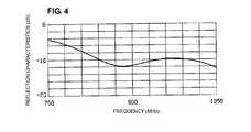
- FIG. 4is a graph representing reflection characteristics of the first preferred embodiment of the present invention.
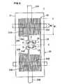
- FIG. 5is a plan view illustrating the electromagnetic coupler module in a wireless IC device in accordance with a second preferred embodiment of the present invention.
- FIG. 6is a plan view illustrating the electromagnetic coupler module in a wireless IC device in accordance with a third preferred embodiment of the present invention.
- FIG. 7is a plan view illustrating the electromagnetic coupler module in a wireless IC device in accordance with a fourth preferred embodiment of the present invention.
- FIG. 8is a plan view illustrating the electromagnetic coupler module in a wireless IC device in accordance with a fifth preferred embodiment of the present invention.
- FIG. 9is a plan view illustrating a wireless IC device in accordance with a sixth preferred embodiment of the present invention.
- FIG. 10is a plan view illustrating the electromagnetic coupler module of the sixth preferred embodiment of the present invention.
- FIG. 11is a perspective view illustrating a wireless IC device in accordance with a seventh preferred embodiment of the present invention.
- FIGS. 12A and 12Billustrate the electromagnetic coupler module of the seventh preferred embodiment, wherein FIG. 12A is a plan view of the module and FIG. 12B is a bottom view of the module.
- FIGS. 1 , 2 and 3illustrate a first preferred embodiment of the wireless IC device.
- the wireless IC deviceincludes a wireless IC chip 5 arranged to process transmission and reception signals at predetermined frequencies, a feeder circuit board 20 having a feeder circuit 22 including a first coupler 23 A and a second coupler 23 B and inductance elements including line electrodes 24 A and 24 B, and a first radiation plate 30 A and a second radiation plate 30 B defining an antenna and arranged on a board 31 preferably made of an PET film, for example.
- the wireless IC chip 5is mounted on the feeder circuit board 20 and both the wireless IC chip 5 and the feeder circuit board 20 define an electromagnetic coupler module 1 .
- the first and second radiation plates 30 A and 30 Bare preferably metal strips that are linearly arranged on the flexible film board 31 , and function as a dipole antenna. Ends of each of the first and second radiation plates 30 A and 30 B are provided with first and second mounts 30 A′ and 30 B′ which respectively support a feeder circuit board 20 .
- the feeder circuit board 20is glued on the first and second mounts 30 A′ and 30 B′ using an adhesive agent (not shown), and the first and second mounts 30 A′ and 30 B′ are electromagnetically coupled with first and second couplers 23 A and 23 B as described below.
- the feeder circuit board 20includes line electrodes 24 A and 24 B meandering on the board 21 preferably made of a PET film, for example. Ends of the line electrodes 24 A and 24 B respectively define connection electrodes 24 A′ and 24 B′, and the other ends thereof are shortcircuited to each other via an electrode 25 . Furthermore, floating electrodes 26 are provided on the flexible film board 21 .
- the line electrodes 24 A and 24 B and the radiation plates 30 A and 30 Bare preferably produced by gluing boards 21 and 31 on a metal thin film, made of an electrically conductive material, such as aluminum foil or copper foil, for example, or by forming a metal plate of Al, Cu, Ag, or other suitable metal, for example, or an electrically conductive paste on the boards 21 and 31 .
- a metal thin filmmade of an electrically conductive material, such as aluminum foil or copper foil, for example, or by forming a metal plate of Al, Cu, Ag, or other suitable metal, for example, or an electrically conductive paste on the boards 21 and 31 .
- the wireless IC chip 5includes a clock circuit, a logic circuit, and a memory circuit, and stores necessary information. As illustrated in FIG. 3 , input and output terminal electrodes 6 and mounting terminal electrodes 7 are arranged on the bottom surface of the wireless IC chip 5 . In the wireless IC chip 5 , the input and output terminal electrodes 6 are electrically connected to the connection electrodes 24 A′ and 24 B′ of the line electrodes 24 A and 24 B via metal bumps preferably made of solder or Au, for example. The mounting terminal electrodes 7 are electrically connected to electrodes 26 via metal bumps.
- the wireless IC deviceis glued on or otherwise affixed to a container of goods as a handling target of the RFID system.
- the wireless IC chip 5communicates with a reader/writer via the feeder circuit 22 and the first and second radiation plates 30 A and 30 B using a high frequency signal on the UHF frequency band. More specifically, the wireless IC chip 5 is operated by the feeder circuit 22 in response to the high frequency signal received by the first and second radiation plates 30 A and 30 B. A response signal from the wireless IC chip 5 is then emitted via the feeder circuit 22 from the radiation plates 30 A and 30 B.
- the first mount 30 A′ of the first radiation plate 30 Ais electromagnetically coupled with the first coupler 23 A and the second mount 30 B′ of the second radiation plate 30 B is electromagnetically coupled with the second coupler 23 B.
- Each of the line electrodes 24 A and 24 Bdefines a resonator circuit with the inductance thereof and a capacitance provided by the lines thereof.
- the resonator circuitis electromagnetically coupled with each of the first mount 30 A′ and the second mount 30 B′.
- the resonator circuitperforms impedance matching and determines a resonance frequency of a signal between the wireless IC chip 5 and each of the radiation plates 30 A and 30 B.
- FIG. 4illustrates reflection characteristics of the wireless IC device. Excellent reflection characteristics equal to or greater than about 10 dB are obtained in at approximately 900 MHz, for example.
- the infinitesimal wireless IC chip 5is electrically connected to and mounted on a small feeder circuit board 20 .
- the mounting of the wireless IC chip 5is easy.
- the feeder electrode 22is not directly electrically connected to the first and second radiation plates 30 A and 30 B, and the first and second couplers 23 A and 23 B are electromagnetically coupled with the first and second mounts 30 A′ and 30 B′.
- the required mounting accuracy with which the feeder circuit board 20 is mounted on (glued on with an adhesive agent) the first and second radiation plates 30 A and 30 Bis reduced.
- the feeder electrode 22can also be miniaturized.
- the operating frequency of the wireless IC deviceis determined by the resonator circuit included in the feeder circuit 22 and thus does not depend on the length of the radiation plates 30 A and 30 B. Even if the feeder circuit board 20 is mounted on the first and second mounts 30 A′ and 30 B′ with some degree of deviation, no operational malfunction occurs. In this sense, as well, the required mounting accuracy is reduced.
- the feeder circuit 22is not directly conductively connected to the first and second radiation plates 30 A and 30 B, the wireless IC chip 5 is prevented from being damaged by an electrostatic charge as an energy wave equal to or less than about 200 MHz entering via the radiation plates 30 A and 30 B.
- a width W 1 of the first coupler 23 A and the second coupler 23 Bis preferably set to be greater than a width W 2 of the first mount 30 A′ and the second mount 30 B′. In this manner, the first and second mounts 30 A′ and 30 B′ are easily aligned with the couplers 23 A and 23 B. The required mounting accuracy of the feeder circuit board 20 with respect to the radiation plates 30 A and 30 B is further reduced. This is also true of each of the preferred embodiments described below.
- the wireless IC deviceis further miniaturized. Furthermore, the first coupler 23 A and the first mount 30 A′ substantially perpendicularly cross each other and the second coupler 23 B and the second mount 30 B′ substantially perpendicularly cross each other. Magnetic fields generated at the couplers 23 A and 23 B and at the mounts 30 A′ and 30 B′ are substantially perpendicular to each other. With this arrangement, the magnetic fields are easily coupled with each other. A power transfer efficiency between the feeder circuit 22 and each of the radiation plates 30 A and 30 B is increased.
- the first coupler 23 A and the second coupler 23 Binclude the line electrodes 24 A and 24 B that are arranged to be axisymmetrical with each other with respect to an axis C centered on the wireless IC chip 5 .
- the first and second mounts 30 A′ and 30 B′are coupled with the feeder circuit 22 at the same constant, and the first radiation plate 30 A and the second radiation plate 30 B can have the same or substantially the same radiation characteristics and the same or substantially the same directivity characteristics. The same is true of the preferred embodiments described below.
- the feeder circuit 22Since the first coupler 23 A and the second coupler 23 B are defined by the meandering line electrodes 24 A and 24 B, the feeder circuit 22 has a compact arrangement.
- the feeder circuit board 20is also miniaturized.
- FIG. 5illustrates a wireless IC device of a second preferred embodiment of the present invention.
- the wireless IC deviceincludes the meandering line electrodes 24 A and 24 B defining the first coupler 23 A and the second coupler 23 B of the feeder circuit 22 arranged on the feeder circuit board 20 .
- the line electrodes 24 A and 24 Bare partially branched (branch points are denoted by reference numerals 27 ).
- the remainder of the structure of the second preferred embodimentis substantially the same as the structure of the first preferred embodiment of the present invention.
- the operation and advantages of the second preferred embodimentare substantially the same as those of the first preferred embodiment.
- the line electrodes 24 A and 24 Bare branched, and the branched portions have different lengths.
- the first coupler 23 A and the second coupler 23 Bprovide a plurality of different frequencies. Frequencies of peak gains of the first and second radiation plates 30 A and 30 B functioning as the antennas are varied. Wide-band gain characteristics are produced accordingly.
- the remainder of the operation and advantagesare substantially the same as the operation and advantages of the first preferred embodiment of the present invention.
- FIG. 6illustrates a wireless IC device of a third preferred embodiment of the present invention.
- the wireless IC deviceincludes the meandering line electrodes 24 A and 24 B including the first coupler 23 A and the second coupler 23 B of the feeder circuit 22 arranged on the feeder circuit board 20 .
- the line electrodes 24 A and 24 Bare bent to extend and meander within a rectangular shape along the longitudinal direction of the board 21 .
- the first mount 30 A′ of the first radiation plate 30 A and the second mount 30 B′ of the second radiation plate 30 Bhave a substantial T shape, and respectively substantially perpendicularly cross the first coupler 23 A and the second coupler 23 B in plan view.
- the remainder of the structure of the third preferred embodimentis substantially the same as that of first preferred embodiment, and the operation and advantages of the third preferred embodiment are substantially the same as the operation and advantages of the first preferred embodiment of the present invention.
- FIG. 7illustrates a wireless IC device of a fourth preferred embodiment of the present invention.
- the wireless IC deviceincludes the spiraling line electrodes 24 A and 24 B defining the first coupler 23 A and the second coupler 23 B of the feeder circuit 22 arranged on the feeder circuit board 20 .
- the first mount 30 A′ of the first radiation plate 30 A and the second mount 30 B′ of the second radiation plate 30 Bhave a substantial T shape.
- the remainder of the structure of the fourth preferred embodimentis substantially the same as the structure of the first preferred embodiment.
- the operation and advantages of the fourth preferred embodimentare substantially the same as the operation and advantages of the first preferred embodiment.
- the first and second spiraling couplers 23 A and 23 Benables the feeder circuit 22 to be designed in a compact arrangement and the feeder circuit board 20 to be miniaturized. Since areas in which the first and second couplers 23 A and 23 B substantially perpendicularly cross the first and second mounts 30 A′ and 30 B′ are increased, the degree of coupling between the magnetic fields generated by the couplers 23 A and 23 B and the mounts 30 A′ and 30 B′ is increased.
- FIG. 8illustrates a wireless IC device of a fifth preferred embodiment of the present invention.
- the wireless IC deviceincludes the line electrodes 24 A and 24 B defining doubly spiraling the feeder circuit 22 arranged on the feeder circuit board 20 .
- the line electrodes 24 A and 24 Bare folded back at electrodes 28 A and 28 B with the ends thereof shortcircuited to each other.
- the remainder of the structure of the fifth preferred embodimentis substantially the same as the structure of the first preferred embodiment, and the operation and advantages of the fifth preferred embodiment are substantially the same as the operation and advantages of the first preferred embodiment.
- the line lengths of the line electrodes 24 A and 24 Bare different from one another by doubling spiraling the line electrodes 24 A and 24 B or by branching the line electrodes 24 A and 24 B at predetermined locations as discussed with reference to the second preferred embodiment.
- the resonance frequencies thereofcan be made different by introducing a different line width or an inter-electrode capacitance.
- the inductance of each electrodecan be varied by changing the width of the electrode. More specifically, as the width of the electrode increases, the inductance of the electrode increases.
- the inter-electrode capacitancecan be varied by changing the spacing between the electrodes. More specifically, as the electrode spacing increases, the capacitance decreases.
- the resonance frequencycan be fine-adjusted by changing the line width and/or the electrode spacing.
- FIGS. 9 and 10illustrate a wireless IC device of a sixth preferred embodiment of the present invention.
- the wireless IC deviceincludes the electromagnetic coupler module 1 including the wireless IC chip 5 and the feeder circuit board 20 .
- the first mount 30 A′ of the first radiation plate 30 Ais electromagnetically coupled with the first coupler 23 A of the feeder circuit 22 and the second mount 30 B′ of the second radiation plate 30 B is electromagnetically coupled with the second coupler 23 B.
- the feeder electrode 22 provided on the feeder circuit board 20is substantially the same as that in the first preferred embodiment.
- the first and second radiation plates 30 A and 30 Bare constructed of meandering metal strips on the flexible board 31 .
- the first mount 30 A′ and the second mount 30 B′ provided on ends of the first and second radiation plates 30 A and 30 Boverlap and cross the first coupler 23 A and the second coupler 23 B defined by the line electrodes 24 A and 24 B for electromagnetic coupling, and the other ends of each the first and second radiation plates 30 A and 30 B are terminated with closed loops.
- the remainder of the structure of the sixth preferred embodimentis substantially the same as the structure of the first preferred embodiment.
- the operation and advantages of the sixth preferred embodimentsubstantially the same as the operation and advantages of the first preferred embodiment.
- the use of the first and second meandering radiation plates 30 A and 30 Benables the radiation plates 30 A and 30 B to have a compact arrangement.
- FIGS. 11 , 12 A and 12 Billustrate a wireless IC device of a seventh preferred embodiment of the present invention.
- the wireless IC deviceincludes the electromagnetic coupler module 1 including the wireless IC chip 5 and the feeder circuit board 20 .
- the feeder electrode 22is provided on the top surface and the bottom surface of the board 21 and the first and second mounts 30 A′ and 30 B′ arranged at ends of the first and second meandering radiation plates 30 A and 30 B are meshed.
- the first and second couplers 23 A and 23 B including the spiraling line electrodes 24 A and 24 Bare arranged on the top surface of the board 21
- the first and second couplers 23 A and 23 B including the spiraling line electrodes 24 A and 24 Bare arranged on the bottom surface of the board 21 .
- the first and second couplers 23 A and 23 B arranged on the top surface and the bottom surface of the board 21are respectively electromagnetically coupled.
- the bottom surface of the flexible film board 21is glued on the first and second mounts 30 A′ and 30 B′ of the first and second radiation plates 30 A and 30 B with an adhesive agent (note shown).
- the first coupler 23 Ais electromagnetically coupled with the first mount 30 A′
- the second coupler 23 Bis electromagnetically coupled with the second mount 30 B′.
- the operation and advantages of the seventh preferred embodimentare substantially the same as the operation and advantages of the first preferred embodiment. Since the first and second couplers 23 A and 23 B are arranged on both the top surface and the bottom surface, the design flexibility of the line electrodes 24 A and 24 B (inductance elements) defining the feeder circuit 22 is increased, and the feeder circuit 22 is thus miniaturized. Since the first and second mounts 30 A′ and 30 B′ of the first and second radiation plates 30 A and 30 B are meshed, the magnetic flux generated by the feeder circuit 22 passes through apertures of the mounts. A change (reduction) in the magnetic flux is reduced. Since more magnetic flux passes through the mounts 30 A′ and 30 B′, transfer efficiency of signal energy is increased.
- the line electrodes 24 A and 24 B of the first and second couplers 23 A and 23 Bare arranged on the top and bottom surfaces of the flexible film board 21 .
- One of the first and second couplers 23 A and 23 Bmay be arranged on both the top and bottom surfaces of the board 21 .
- one of the first and second mounts 30 A′ and 30 B′may be meshed.
- the width of the first coupler and the second coupleris preferably greater than the width of the first mount and the second mount. This arrangement facilitates the position alignment between the mount and the coupler. The required mounting accuracy of the feeder circuit board with respect to the mount is reduced.
- the first coupler and the first mountmay preferably partially overlap each other in plan view and the second coupler and the second mount may preferably partially overlap each other in plan view.
- the wireless IC devicecan be further miniaturized. If the two elements cross each other, the magnetic fields of the two elements are easily coupled and the transfer efficiency of power between the feeder circuit and the radiation plate is increased.
- At least one of the first mount and the second mountmay preferably be meshed. Since the magnetic flux generated by the feeder circuit passes through the apertures, a change (reduction) in the magnetic flux is reduced. Since more magnetic flux passes through the mounts, transfer efficiency of signal energy is increased.
- At least one of the first coupler and the second couplermay preferably be arranged on both the top and bottom surfaces of the feeder circuit board. With the coupler arranged on both the top and bottom surfaces of the feeder circuit board, the design flexibility of the inductance element defining the feeder circuit is increased. The feeder circuit is thus miniaturized.
- first coupler and the second couplermay preferably be axisymmetrical to each other with respect to the center of the wireless IC chip.
- the first and second radiation platesare preferably coupled with the feeder circuit with the same constant.
- the first and second radiation platescan have the same radiation characteristics and the same directivity characteristics, for example.
- Each of the first coupler and the second couplermay preferably be constructed of a continuous line electrode, or a line electrode meandering or spiraling, for example.
- the line electrodemay be branched at a predetermined position.
- the meandering structure or the spiraling structureenables the feeder circuit to be produced so as to have a compact arrangement, thereby contributing to the miniaturization of the feeder circuit board. If the lengths of the line electrodes are varied, a plurality of resonance frequencies are provided. The frequencies of the peak gains of the first and second radiation plates functioning the antenna are varied, and wide-band gain characteristics are obtained.
- the resonance frequency of the line electrodeis determined by the line length thereof. Even if the line lengths of the line electrodes are different, the resonance frequencies of the line electrodes can be made different by providing different the inter-electrode capacitances, for example. More specifically, the inductance of the electrode is varied by changing the line width of the line electrode. The capacitance of the inter-electrode is varied by changing the electrode spacing.
- the feeder circuit boardmay be a flexible board. Since the flexible board is typically thin, the wireless IC device may be produced in a low-profile structure.
- the wireless IC device of the present inventionis not limited to the above-described preferred embodiments, and a variety of modification may be implemented in the invention without departing from the scope of the invention.
- the materials of the line electrodes 24 A and 24 B, the radiation plates 30 A and 30 B, and the boards 21 and 31are described for exemplary purposes only. Any material can be used as long as the material has the required characteristics.
- the wireless IC chip 5may be connected to the feeder circuit 22 through another process different from the one using the metal bump, for example.
- preferred embodiments of the present inventionare useful for the wireless IC device, and are particularly advantageous in that miniaturization is achieved without the need for high-precision mounting.
Landscapes
- Engineering & Computer Science (AREA)
- Microelectronics & Electronic Packaging (AREA)
- Computer Hardware Design (AREA)
- Physics & Mathematics (AREA)
- General Physics & Mathematics (AREA)
- Theoretical Computer Science (AREA)
- Details Of Aerials (AREA)
- Variable-Direction Aerials And Aerial Arrays (AREA)
- Devices For Checking Fares Or Tickets At Control Points (AREA)
- Credit Cards Or The Like (AREA)
- Junction Field-Effect Transistors (AREA)
Abstract
Description
Claims (20)
Applications Claiming Priority (5)
| Application Number | Priority Date | Filing Date | Title |
|---|---|---|---|
| JP2007-168625 | 2007-06-27 | ||
| JP2007168625 | 2007-06-27 | ||
| JP2007-232844 | 2007-09-07 | ||
| JP2007232844 | 2007-09-07 | ||
| PCT/JP2008/061442WO2009001814A1 (en) | 2007-06-27 | 2008-06-24 | Wireless ic device |
Related Parent Applications (1)
| Application Number | Title | Priority Date | Filing Date |
|---|---|---|---|
| PCT/JP2008/061442ContinuationWO2009001814A1 (en) | 2007-06-27 | 2008-06-24 | Wireless ic device |
Publications (2)
| Publication Number | Publication Date |
|---|---|
| US20090201156A1 US20090201156A1 (en) | 2009-08-13 |
| US8264357B2true US8264357B2 (en) | 2012-09-11 |
Family
ID=40185628
Family Applications (1)
| Application Number | Title | Priority Date | Filing Date |
|---|---|---|---|
| US12/429,346ActiveUS8264357B2 (en) | 2007-06-27 | 2009-04-24 | Wireless IC device |
Country Status (7)
| Country | Link |
|---|---|
| US (1) | US8264357B2 (en) |
| EP (1) | EP2077602B1 (en) |
| JP (1) | JP4396785B2 (en) |
| KR (1) | KR101062124B1 (en) |
| CN (1) | CN101558530B (en) |
| AT (1) | ATE545174T1 (en) |
| WO (1) | WO2009001814A1 (en) |
Cited By (1)
| Publication number | Priority date | Publication date | Assignee | Title |
|---|---|---|---|---|
| US9887464B2 (en)* | 2015-10-22 | 2018-02-06 | Ajou University Industry-Academic Cooperation Foundation | Compact dipole antenna for RFID tag |
Families Citing this family (13)
| Publication number | Priority date | Publication date | Assignee | Title |
|---|---|---|---|---|
| CN102498617B (en)* | 2009-09-09 | 2015-04-01 | 株式会社村田制作所 | Antenna, manufacturing method thereof, and wireless IC device |
| JP2011182392A (en)* | 2010-02-08 | 2011-09-15 | Sinfonia Technology Co Ltd | Dipole-type ic tag antenna, antenna roll and method of using ic tag |
| CN102403570B (en)* | 2010-09-10 | 2013-09-25 | 航天信息股份有限公司 | Tag antenna and electronic tag |
| US9299021B2 (en)* | 2010-11-11 | 2016-03-29 | Avery Dennison Corporation | RFID devices and methods for manufacturing |
| WO2012093541A1 (en)* | 2011-01-05 | 2012-07-12 | 株式会社村田製作所 | Wireless communication device |
| WO2013035821A1 (en)* | 2011-09-09 | 2013-03-14 | 株式会社村田製作所 | Antenna device and wireless device |
| CN103606002A (en)* | 2013-11-30 | 2014-02-26 | 陈其晖 | RFID electronic tag and antenna thereof |
| US10268940B2 (en)* | 2014-10-01 | 2019-04-23 | Ohio State Innovation Foundation | Stretchable broad impedance bandwidth RFID devices |
| KR102175750B1 (en)* | 2014-10-29 | 2020-11-06 | 삼성전자주식회사 | Antenna device for electronic device with the same |
| CN104485508A (en)* | 2014-12-19 | 2015-04-01 | 夏景 | Complex impedance RFID (radio frequency identification) bow-tie-shaped printing antenna |
| FR3033436B1 (en)* | 2015-03-04 | 2018-05-25 | Smart Packaging Solutions | MICROELECTRONIC COMPONENT FOR NON-CONTACT OPERATING CHIP CARD |
| CN209913045U (en)* | 2017-07-21 | 2020-01-07 | 株式会社村田制作所 | wireless communication device |
| CN109728403B (en)* | 2018-12-28 | 2023-09-01 | 浙江中烟工业有限责任公司 | Single-port feed dual-polarized far-field/near-field antenna for forklift reader |
Citations (208)
| Publication number | Priority date | Publication date | Assignee | Title |
|---|---|---|---|---|
| US3364564A (en) | 1965-06-28 | 1968-01-23 | Gregory Ind Inc | Method of producing welding studs dischargeable in end-to-end relationship |
| JPS50143451A (en) | 1974-05-08 | 1975-11-18 | ||
| JPS62127140U (en) | 1986-02-03 | 1987-08-12 | ||
| US4794397A (en) | 1984-10-13 | 1988-12-27 | Toyota Jidosha Kabushiki Kaisha | Automobile antenna |
| JPH03262313A (en) | 1990-03-13 | 1991-11-22 | Murata Mfg Co Ltd | band pass filter |
| NL9100176A (en) | 1991-02-01 | 1992-03-02 | Nedap Nv | Antenna configuration for contactless identification label - forms part of tuned circuit of ID or credit card interrogated via inductive coupling |
| NL9100347A (en) | 1991-02-26 | 1992-03-02 | Nedap Nv | Integrated transformer circuit for ID or credit card - is interrogated via contactless inductive coupling using capacitor to form tuned circuit |
| JPH04150011A (en) | 1990-10-12 | 1992-05-22 | Tdk Corp | Composite electronic component |
| US5232765A (en) | 1990-07-25 | 1993-08-03 | Ngk Insulators, Ltd. | Distributed constant circuit board using ceramic substrate material |
| US5253969A (en) | 1989-03-10 | 1993-10-19 | Sms Schloemann-Siemag Aktiengesellschaft | Feeding system for strip material, particularly in treatment plants for metal strips |
| JPH05327331A (en) | 1992-05-15 | 1993-12-10 | Matsushita Electric Works Ltd | Printed antenna |
| JPH0653733A (en) | 1992-07-30 | 1994-02-25 | Murata Mfg Co Ltd | Resonator antenna |
| JPH0677729A (en) | 1992-08-25 | 1994-03-18 | Mitsubishi Electric Corp | Antenna integrated microwave circuit |
| JPH06177635A (en) | 1992-12-07 | 1994-06-24 | Mitsubishi Electric Corp | Cross dipole antenna system |
| US5337063A (en) | 1991-04-22 | 1994-08-09 | Mitsubishi Denki Kabushiki Kaisha | Antenna circuit for non-contact IC card and method of manufacturing the same |
| US5374937A (en) | 1991-07-08 | 1994-12-20 | Nippon Telegraph And Telephone Corporation | Retractable antenna system |
| JPH07183836A (en) | 1993-12-22 | 1995-07-21 | San'eisha Mfg Co Ltd | Coupling filter device for distribution line carrier communication |
| EP0694874A2 (en) | 1994-07-25 | 1996-01-31 | Toppan Printing Co., Ltd. | Biodegradable cards |
| US5491483A (en) | 1994-01-05 | 1996-02-13 | Texas Instruments Incorporated | Single loop transponder system and method |
| JPH0856113A (en) | 1994-08-11 | 1996-02-27 | Matsushita Electric Ind Co Ltd | Millimeter wave detector |
| JPH0887580A (en) | 1994-09-14 | 1996-04-02 | Omron Corp | Data carrier and ball game |
| JPH08176421A (en) | 1994-12-26 | 1996-07-09 | Toppan Printing Co Ltd | Biodegradable laminate and biodegradable card |
| JPH08279027A (en) | 1995-04-04 | 1996-10-22 | Toshiba Corp | Wireless communication card |
| JPH08307126A (en) | 1995-05-09 | 1996-11-22 | Kyocera Corp | Antenna storage structure |
| US5757074A (en) | 1995-07-07 | 1998-05-26 | Hughes Electronics Corporation | Microwave/millimeter wave circuit structure with discrete flip-chip mounted elements |
| JPH11149537A (en) | 1997-11-14 | 1999-06-02 | Toppan Printing Co Ltd | Composite IC card and composite IC module |
| US5936150A (en) | 1998-04-13 | 1999-08-10 | Rockwell Science Center, Llc | Thin film resonant chemical sensor with resonant acoustic isolator |
| US5955723A (en) | 1995-05-03 | 1999-09-21 | Siemens Aktiengesellschaft | Contactless chip card |
| US5995006A (en) | 1995-09-05 | 1999-11-30 | Intermec Ip Corp. | Radio frequency tag |
| JP2000021639A (en) | 1998-07-02 | 2000-01-21 | Sharp Corp | Inductor, resonance circuit, matching circuit, antenna circuit and oscillation circuit using the same |
| JP2000022421A (en) | 1998-07-03 | 2000-01-21 | Murata Mfg Co Ltd | Chip antenna and radio device mounted with it |
| EP0977145A2 (en) | 1998-07-28 | 2000-02-02 | Kabushiki Kaisha Toshiba | Radio IC card |
| WO2000010122A2 (en) | 1998-08-14 | 2000-02-24 | 3M Innovative Properties Company | Radio frequency identification systems applications |
| JP2000059260A (en) | 1998-08-04 | 2000-02-25 | Sony Corp | Storage device |
| JP2000085283A (en) | 1998-09-16 | 2000-03-28 | Dainippon Printing Co Ltd | Non-contact IC card and method of manufacturing the same |
| JP2000090207A (en) | 1998-09-08 | 2000-03-31 | Toppan Printing Co Ltd | Non-contact IC card inspection apparatus and inspection method |
| JP2000132643A (en) | 1998-10-23 | 2000-05-12 | Toppan Printing Co Ltd | Inspection apparatus and inspection method for non-contact IC card |
| JP2000137778A (en) | 1998-10-30 | 2000-05-16 | Denso Corp | Id tag for dish type article |
| JP2000148948A (en) | 1998-11-05 | 2000-05-30 | Sony Corp | Non-contact ic label and its manufacture |
| JP2000172812A (en) | 1998-12-08 | 2000-06-23 | Hitachi Maxell Ltd | Noncontact information medium |
| JP2000510271A (en) | 1997-01-28 | 2000-08-08 | アマテック アドヴァンスト マイクロメカニック アンド オートメーション テクノロジー ゲゼルシャフト ミット ベシュレンクテル ハフツング ウント コンパニー.コマンディト ゲゼルシャフト | Transmission module for transponder device, transponder device, and method of operating transponder device |
| US6104311A (en) | 1996-08-26 | 2000-08-15 | Addison Technologies | Information storage and identification tag |
| US6107920A (en) | 1998-06-09 | 2000-08-22 | Motorola, Inc. | Radio frequency identification tag having an article integrated antenna |
| JP2000276569A (en) | 1999-03-26 | 2000-10-06 | Dainippon Printing Co Ltd | IC chip and memory medium incorporating the same |
| JP2000286634A (en) | 1999-03-30 | 2000-10-13 | Ngk Insulators Ltd | Antenna system and its manufacture |
| JP2000286760A (en) | 1999-03-31 | 2000-10-13 | Toyota Autom Loom Works Ltd | Coupler for mobile communication, mobile object and communication method for mobile object |
| JP2000311226A (en) | 1998-07-28 | 2000-11-07 | Toshiba Corp | Wireless IC card, manufacturing method thereof, and wireless IC card read / write system |
| JP2000321984A (en) | 1999-05-12 | 2000-11-24 | Hitachi Ltd | Label with RF-ID tag |
| US6172608B1 (en) | 1996-06-19 | 2001-01-09 | Integrated Silicon Design Pty. Ltd. | Enhanced range transponder system |
| JP2001028036A (en) | 1999-07-14 | 2001-01-30 | Shinko Electric Ind Co Ltd | Semiconductor device and its manufacture |
| US6181287B1 (en)* | 1997-03-10 | 2001-01-30 | Precision Dynamics Corporation | Reactively coupled elements in circuits on flexible substrates |
| JP2001043340A (en) | 1999-07-29 | 2001-02-16 | Toppan Printing Co Ltd | Composite IC card |
| JP3075400U (en) | 2000-08-03 | 2001-02-16 | 昌栄印刷株式会社 | Non-contact IC card |
| US6190942B1 (en) | 1996-10-09 | 2001-02-20 | Pav Card Gmbh | Method and connection arrangement for producing a smart card |
| JP2001168628A (en) | 1999-12-06 | 2001-06-22 | Smart Card Technologies:Kk | Auxiliary antenna for IC card |
| US6259369B1 (en) | 1999-09-30 | 2001-07-10 | Moore North America, Inc. | Low cost long distance RFID reading |
| JP2001240046A (en) | 2000-02-25 | 2001-09-04 | Toppan Forms Co Ltd | Container and manufacturing method thereof |
| JP2001256457A (en) | 2000-03-13 | 2001-09-21 | Toshiba Corp | Semiconductor device, manufacturing method thereof, and IC card communication system |
| JP2001319380A (en) | 2000-05-11 | 2001-11-16 | Mitsubishi Materials Corp | Optical disk with rfid |
| JP2001331976A (en) | 2000-05-17 | 2001-11-30 | Casio Comput Co Ltd | Optical recording type recording medium |
| JP2001332923A (en) | 2000-05-19 | 2001-11-30 | Dx Antenna Co Ltd | Film antenna |
| JP2001344574A (en) | 2000-05-30 | 2001-12-14 | Mitsubishi Materials Corp | Antenna device for interrogator |
| JP2001351084A (en) | 2000-04-04 | 2001-12-21 | Dainippon Printing Co Ltd | Non-contact data carrier device and auxiliary antenna |
| JP2001352176A (en) | 2000-06-05 | 2001-12-21 | Fuji Xerox Co Ltd | Multilayer printed wiring board and manufacturing method of multilayer printed wiring board |
| US6335686B1 (en) | 1998-08-14 | 2002-01-01 | 3M Innovative Properties Company | Application for a radio frequency identification system |
| JP2002024776A (en) | 2000-07-07 | 2002-01-25 | Nippon Signal Co Ltd:The | Ic card reader/writer |
| JP2002042076A (en) | 2000-07-21 | 2002-02-08 | Dainippon Printing Co Ltd | Non-contact data carrier and booklet having non-contact data carrier |
| JP2002505645A (en) | 1998-04-14 | 2002-02-19 | リバティ・カートン・カンパニー−テキサス | Container for compressors and other goods |
| JP2002063557A (en) | 2000-08-21 | 2002-02-28 | Mitsubishi Materials Corp | Tag for rfid |
| US6362784B1 (en) | 1998-03-31 | 2002-03-26 | Matsuda Electric Industrial Co., Ltd. | Antenna unit and digital television receiver |
| US6367143B1 (en) | 1998-03-10 | 2002-04-09 | Smart Card Technologies Co. Ltd. | Coil element and method for manufacturing thereof |
| US20020044092A1 (en) | 2000-08-24 | 2002-04-18 | Yuichi Kushihi | Antenna device and radio equipment having the same |
| US6378774B1 (en) | 1997-11-14 | 2002-04-30 | Toppan Printing Co., Ltd. | IC module and smart card |
| JP2002150245A (en) | 2000-10-19 | 2002-05-24 | Samsung Sds Co Ltd | IC module for IC card and IC card using the same |
| US20020067316A1 (en) | 2000-10-27 | 2002-06-06 | Mitsubishi Materials Corporation | Antenna |
| US6406990B1 (en) | 1999-11-24 | 2002-06-18 | Omron Corporation | Method of mounting a semiconductor chip, circuit board for flip-chip connection and method of manufacturing the same, electromagnetic wave readable data carrier and method of manufacturing the same, and electronic component module for an electromagnetic wave readable data carrier |
| JP2002175508A (en) | 2000-12-07 | 2002-06-21 | Dainippon Printing Co Ltd | Non-contact data carrier device and wiring member for booster antenna |
| JP2002185358A (en) | 2000-11-24 | 2002-06-28 | Supersensor Pty Ltd | Method for fitting rf transponder to container |
| JP2002183690A (en) | 2000-12-11 | 2002-06-28 | Hitachi Maxell Ltd | Non-contact IC tag device |
| JP2002230128A (en) | 2001-02-05 | 2002-08-16 | Dainippon Printing Co Ltd | Article with coil-on-chip type semiconductor module and sales system |
| JP2002252117A (en) | 2000-12-19 | 2002-09-06 | Murata Mfg Co Ltd | Laminated coil component and its manufacturing method |
| US6448874B1 (en) | 1999-02-08 | 2002-09-10 | Alps Electric Co., Ltd. | Resonant line constructed by microstrip line which is easy to be trimmed |
| JP2002298109A (en) | 2001-03-30 | 2002-10-11 | Toppan Forms Co Ltd | Non-contact IC media and method of manufacturing the same |
| JP2002319008A (en) | 2001-04-23 | 2002-10-31 | Hanex Chuo Kenkyusho:Kk | Rfid tag structure and method of manufacturing it |
| US20020171591A1 (en)* | 2001-05-17 | 2002-11-21 | Paul Beard | Ball grid array antenna |
| JP2002362613A (en) | 2001-06-07 | 2002-12-18 | Toppan Printing Co Ltd | Laminated packaging material in which non-contact IC is laminated, packaging container using the same, and method for detecting opening of packaging container |
| JP2002373029A (en) | 2001-06-18 | 2002-12-26 | Hitachi Ltd | How to prevent unauthorized copying of software using IC tags |
| JP2002373323A (en) | 2001-06-18 | 2002-12-26 | Dainippon Printing Co Ltd | Card-integrated foam with non-contact IC chip |
| JP2002374139A (en) | 2001-06-13 | 2002-12-26 | Murata Mfg Co Ltd | Balance type lc filter |
| JP2003006599A (en) | 2001-06-19 | 2003-01-10 | Teraoka Seiko Co Ltd | Method for mounting ic tag on metal object and marker with built-in ic tag |
| JP2003016412A (en) | 2001-07-03 | 2003-01-17 | Hitachi Chem Co Ltd | Ic module, ic label, and ic card |
| US20030020661A1 (en) | 2001-07-27 | 2003-01-30 | Tdk Corporation | Antenna device capable of being commonly used at a plurality of frequencies and electronic equipment having the same |
| JP2003030612A (en) | 2001-07-19 | 2003-01-31 | Oji Paper Co Ltd | Ic chip mounting body |
| JP2003069335A (en) | 2001-08-28 | 2003-03-07 | Hitachi Kokusai Electric Inc | Auxiliary antenna |
| JP2003067711A (en) | 2001-08-29 | 2003-03-07 | Toppan Forms Co Ltd | Articles with IC chip mounting or antenna part |
| JP2003076947A (en) | 2001-09-05 | 2003-03-14 | Toppan Forms Co Ltd | RF-ID inspection system |
| JP2003085501A (en) | 2001-09-07 | 2003-03-20 | Dainippon Printing Co Ltd | Non-contact IC tag |
| JP2003085520A (en) | 2001-09-11 | 2003-03-20 | Oji Paper Co Ltd | IC card manufacturing method |
| US6542050B1 (en) | 1999-03-30 | 2003-04-01 | Ngk Insulators, Ltd. | Transmitter-receiver |
| JP2003099720A (en) | 2001-09-25 | 2003-04-04 | Toppan Forms Co Ltd | RF-ID inspection system |
| JP2003099721A (en) | 2001-09-25 | 2003-04-04 | Toppan Forms Co Ltd | RF-ID inspection system |
| JP2003110344A (en) | 2001-09-26 | 2003-04-11 | Hitachi Metals Ltd | Surface-mounting type antenna and antenna device mounting the same |
| JP2003132330A (en) | 2001-10-25 | 2003-05-09 | Sato Corp | RFID label printer |
| JP2003134007A (en) | 2001-10-30 | 2003-05-09 | Auto Network Gijutsu Kenkyusho:Kk | Signal transmission / reception system between vehicle-mounted devices and signal transmission / reception method between vehicle-mounted devices |
| JP2003155062A (en) | 2001-11-20 | 2003-05-27 | Dainippon Printing Co Ltd | Package with IC tag and method of manufacturing package with IC tag |
| JP2003158414A (en) | 2001-11-20 | 2003-05-30 | Dainippon Printing Co Ltd | Package with IC tag and method of manufacturing package with IC tag |
| JP2003188338A (en) | 2001-12-13 | 2003-07-04 | Sony Corp | Circuit board and its manufacturing method |
| JP2003187211A (en) | 2001-12-20 | 2003-07-04 | Dainippon Printing Co Ltd | Base material for paper IC card with non-contact communication function |
| JP2003187207A (en) | 2001-12-17 | 2003-07-04 | Mitsubishi Materials Corp | Electrode structure of tag for rfid and method for adjusting resonance frequency using the same electrode |
| JP2003198230A (en) | 2001-12-28 | 2003-07-11 | Ntn Corp | Integrated dielectric resin antenna |
| JP2003209421A (en) | 2002-01-17 | 2003-07-25 | Dainippon Printing Co Ltd | RFID tag having transparent antenna and method of manufacturing the same |
| JP2003218624A (en) | 2002-01-21 | 2003-07-31 | Fec Inc | Booster antenna for ic card |
| JP2003216919A (en) | 2002-01-23 | 2003-07-31 | Toppan Forms Co Ltd | RF-ID media |
| JP2003233780A (en) | 2002-02-06 | 2003-08-22 | Mitsubishi Electric Corp | Data communication device |
| JP2003242471A (en) | 2002-02-14 | 2003-08-29 | Dainippon Printing Co Ltd | Method of forming antenna pattern on IC chip mounted on web and package with IC tag |
| JP2003243918A (en) | 2002-02-18 | 2003-08-29 | Dainippon Printing Co Ltd | Non-contact IC tag antenna and non-contact IC tag |
| JP2003249813A (en) | 2002-02-25 | 2003-09-05 | Tecdia Kk | RFID tag with loop antenna |
| WO2003079305A1 (en) | 2002-03-13 | 2003-09-25 | Celis Semiconductor Corporation | Integrated circuit with enhanced coupling |
| JP2003288560A (en) | 2002-03-27 | 2003-10-10 | Toppan Forms Co Ltd | Interposer and inlet sheet having antistatic function |
| US6634564B2 (en) | 2000-10-24 | 2003-10-21 | Dai Nippon Printing Co., Ltd. | Contact/noncontact type data carrier module |
| JP2003309418A (en) | 2002-04-17 | 2003-10-31 | Alps Electric Co Ltd | Dipole antenna |
| JP2003332820A (en) | 2002-05-10 | 2003-11-21 | Fec Inc | Booster antenna for ic card |
| US20040001027A1 (en) | 2002-06-27 | 2004-01-01 | Killen William D. | Dipole arrangements using dielectric substrates of meta-materials |
| JP2004082775A (en) | 2002-08-23 | 2004-03-18 | Yokohama Rubber Co Ltd:The | Pneumatic tire |
| JP2004096566A (en) | 2002-09-02 | 2004-03-25 | Toenec Corp | Inductive communication equipment |
| US6763254B2 (en) | 2001-03-30 | 2004-07-13 | Matsushita Electric Industrial Co., Ltd. | Portable information terminal having wireless communication device |
| JP2004253858A (en) | 2003-02-18 | 2004-09-09 | Minerva:Kk | Booster antenna device for ic tag |
| JP2004287767A (en) | 2003-03-20 | 2004-10-14 | Hitachi Maxell Ltd | Non-contact communication information carrier |
| JP2004297249A (en) | 2003-03-26 | 2004-10-21 | Matsushita Electric Ind Co Ltd | Coupler between different phases and its mounting method, and coupling method between different phases |
| JP2004297681A (en) | 2003-03-28 | 2004-10-21 | Toppan Forms Co Ltd | Non-contact information recording medium |
| US20040219956A1 (en) | 2003-02-06 | 2004-11-04 | Hiroshi Iwai | Portable radio communication apparatus provided with a boom portion and a part of housing operating as an antenna |
| US20040217915A1 (en) | 2003-05-02 | 2004-11-04 | Tatsuya Imaizumi | Antenna matching circuit, mobile communication device including antenna matching circuit, and dielectric antenna including antenna matching circuit |
| JP2004326380A (en) | 2003-04-24 | 2004-11-18 | Dainippon Printing Co Ltd | RFID tag |
| JP2004334268A (en) | 2003-04-30 | 2004-11-25 | Dainippon Printing Co Ltd | Paper IC tags and books / magazines with paper IC tags, books with paper IC tags |
| JP2004343000A (en) | 2003-05-19 | 2004-12-02 | Fujikura Ltd | Semiconductor module, non-contact IC tag having the same, and method of manufacturing semiconductor module |
| US6828881B2 (en) | 2001-07-02 | 2004-12-07 | Ngk Insulators, Ltd. | Stacked dielectric filter |
| JP2004362190A (en) | 2003-06-04 | 2004-12-24 | Hitachi Ltd | Semiconductor device |
| JP2004362341A (en) | 2003-06-05 | 2004-12-24 | Toppan Printing Co Ltd | IC tag |
| JP2004362602A (en) | 2004-07-26 | 2004-12-24 | Hitachi Ltd | RFID tag |
| US20050092836A1 (en) | 2003-10-29 | 2005-05-05 | Kazuhiro Kudo | Loop coilantenna |
| US20050093677A1 (en)* | 2003-11-04 | 2005-05-05 | Forster Ian J. | RFID tag with enhanced readability |
| JP2005124061A (en) | 2003-10-20 | 2005-05-12 | Toyota Motor Corp | Loop antenna device |
| US20050099337A1 (en) | 2003-11-12 | 2005-05-12 | Hitachi, Ltd. | Antenna, method for manufacturing the antenna, and communication apparatus including the antenna |
| US20050125093A1 (en) | 2003-10-01 | 2005-06-09 | Sony Corporation | Relaying apparatus and communication system |
| JP2005167327A (en) | 2003-11-28 | 2005-06-23 | Sharp Corp | Small antenna and wireless tag provided with the same |
| JP2005165839A (en) | 2003-12-04 | 2005-06-23 | Nippon Signal Co Ltd:The | Reader/writer, ic tag, article control device, and optical disk device |
| US20050140512A1 (en) | 2003-12-25 | 2005-06-30 | Isao Sakama | Wireless IC tag, and method and apparatus for manufacturing the same |
| JP2005191705A (en) | 2003-12-24 | 2005-07-14 | Sharp Corp | Wireless tag and RFID system using the same |
| JP2005190417A (en) | 2003-12-26 | 2005-07-14 | Taketani Shoji:Kk | Fixed object management system and individual identifier for use therein |
| JP2005210680A (en) | 2003-12-25 | 2005-08-04 | Mitsubishi Materials Corp | Antenna device |
| US6927738B2 (en) | 2001-01-11 | 2005-08-09 | Hanex Co., Ltd. | Apparatus and method for a communication device |
| JP2005217822A (en) | 2004-01-30 | 2005-08-11 | Soshin Electric Co Ltd | Antenna device |
| JP2005229474A (en) | 2004-02-16 | 2005-08-25 | Olympus Corp | Information terminal device |
| JP2005236339A (en) | 2001-07-19 | 2005-09-02 | Oji Paper Co Ltd | IC chip assembly |
| JP2005244778A (en) | 2004-02-27 | 2005-09-08 | Sharp Corp | Small antenna and wireless tag provided with the same |
| JP2005275870A (en) | 2004-03-25 | 2005-10-06 | Matsushita Electric Ind Co Ltd | INSERTION TYPE WIRELESS COMMUNICATION MEDIUM DEVICE AND ELECTRONIC DEVICE |
| US20050232412A1 (en) | 2004-04-16 | 2005-10-20 | Matsushita Electric Industrial Co., Ltd. | Line state detecting apparatus and transmitting apparatus and receiving apparatus of balanced transmission system |
| JP2005295135A (en) | 2004-03-31 | 2005-10-20 | Sharp Corp | Television receiver |
| US20050236623A1 (en) | 2004-04-23 | 2005-10-27 | Nec Corporation | Semiconductor device |
| JP2005321305A (en) | 2004-05-10 | 2005-11-17 | Murata Mfg Co Ltd | Electronic component measurement jig |
| WO2005115849A1 (en) | 2004-05-26 | 2005-12-08 | Iwata Label Co., Ltd. | Rfid label attachment method and attachment device |
| JP2005346820A (en) | 2004-06-02 | 2005-12-15 | Funai Electric Co Ltd | Optical disk having radio ic tag and optical disk reproducing device |
| US20050275539A1 (en) | 2004-06-11 | 2005-12-15 | Isao Sakama | Radio frequency IC tag and method for manufacturing the same |
| JP2005352858A (en) | 2004-06-11 | 2005-12-22 | Hitachi Maxell Ltd | Communication record carrier |
| US20060001138A1 (en) | 2004-06-30 | 2006-01-05 | Hitachi, Ltd. | IC-tag-bearing wiring board and method of fabricating the same |
| JP2006031766A (en) | 2004-07-13 | 2006-02-02 | Fujitsu Ltd | RFID tag antenna structure for optical recording medium and optical recording medium storage case with RFID tag antenna |
| US20060038257A1 (en)* | 2004-08-19 | 2006-02-23 | Noritaka Anzai | Semiconductor device which includes an inductor therein and a manufacturing method thereof |
| US20060043198A1 (en)* | 2004-09-01 | 2006-03-02 | Forster Ian J | RFID device with combined reactive coupler |
| US20060044769A1 (en) | 2004-09-01 | 2006-03-02 | Forster Ian J | RFID device with magnetic coupling |
| US20060055601A1 (en) | 2002-07-05 | 2006-03-16 | Shozaburo Kameda | Antenna with built-in filter |
| US20060071084A1 (en) | 2000-12-15 | 2006-04-06 | Electrox Corporation | Process for manufacture of novel, inexpensive radio frequency identification devices |
| JP2006102953A (en) | 2004-09-30 | 2006-04-20 | Brother Ind Ltd | Print head and tag label producing apparatus |
| JP2006148518A (en) | 2004-11-19 | 2006-06-08 | Matsushita Electric Works Ltd | Adjuster and adjusting method of non-contact ic card |
| JP2006174151A (en) | 2004-12-16 | 2006-06-29 | Denso Corp | Ic tag and ic tag attaching structure |
| US20060158380A1 (en) | 2004-12-08 | 2006-07-20 | Hae-Won Son | Antenna using inductively coupled feeding method, RFID tag using the same and antenna impedence matching method thereof |
| JP2006195795A (en) | 2005-01-14 | 2006-07-27 | Hitachi Chem Co Ltd | Ic tag inlet, and manufacturing method for ic tag inlet |
| JP2006203187A (en) | 2004-12-24 | 2006-08-03 | Semiconductor Energy Lab Co Ltd | Semiconductor device |
| US20060170606A1 (en) | 2005-02-01 | 2006-08-03 | Fujitsu Limited | Meander line antenna |
| JP2006203852A (en) | 2004-12-24 | 2006-08-03 | Toppan Forms Co Ltd | Non-contact IC module |
| JP2006232292A (en) | 2005-02-22 | 2006-09-07 | Nippon Sheet Glass Co Ltd | Container with RFID tag and RFID system |
| US7112952B2 (en) | 2004-01-30 | 2006-09-26 | Semiconductor Energy Laboratory Co., Ltd. | Inspection system, inspection method, and method for manufacturing semiconductor device |
| JP2006270212A (en) | 2005-03-22 | 2006-10-05 | Nec Tokin Corp | Wireless tag |
| US7129834B2 (en) | 2002-03-28 | 2006-10-31 | Kabushiki Kaisha Toshiba | String wireless sensor and its manufacturing method |
| JP2006302219A (en) | 2005-04-25 | 2006-11-02 | Fujita Denki Seisakusho:Kk | RFID tag communication range setting device |
| JP2006309401A (en) | 2005-04-27 | 2006-11-09 | Hitachi Chem Co Ltd | Ic tag |
| US20060267138A1 (en) | 2005-05-30 | 2006-11-30 | Semiconductor Energy Laboratory Co., Ltd. | Semiconductor device |
| US20070004028A1 (en) | 2005-03-10 | 2007-01-04 | Gen-Probe Incorporated | Signal measuring system for conducting real-time amplification assays |
| JP2007043535A (en) | 2005-08-04 | 2007-02-15 | Matsushita Electric Ind Co Ltd | Antenna for RF-ID reader / writer device, RF-ID reader / writer device using the antenna, and RF-ID system |
| US20070040028A1 (en) | 2005-08-18 | 2007-02-22 | Fujitsu Limited | RFID tag |
| US20070052613A1 (en) | 2005-09-06 | 2007-03-08 | Sebastian Gallschuetz | Radio frequency identification transponder antenna |
| JP2007122542A (en) | 2005-10-31 | 2007-05-17 | Sato Corp | RFID label and RFID label attaching method |
| JP2007150868A (en) | 2005-11-29 | 2007-06-14 | Renesas Technology Corp | Electronic equipment and method of manufacturing the same |
| US20070164414A1 (en) | 2006-01-19 | 2007-07-19 | Murata Manufacturing Co., Ltd. | Wireless ic device and component for wireless ic device |
| WO2007083574A1 (en) | 2006-01-19 | 2007-07-26 | Murata Manufacturing Co., Ltd. | Radio ic device and radio ic device part |
| US7250910B2 (en) | 2003-02-03 | 2007-07-31 | Matsushita Electric Industrial Co., Ltd. | Antenna apparatus utilizing minute loop antenna and radio communication apparatus using the same antenna apparatus |
| US20070210923A1 (en)* | 2005-12-09 | 2007-09-13 | Butler Timothy P | Multiple radio frequency network node rfid tag |
| WO2007119304A1 (en) | 2006-04-14 | 2007-10-25 | Murata Manufacturing Co., Ltd. | Wireless ic device |
| US20070285335A1 (en) | 2003-12-25 | 2007-12-13 | Mitsubishi Materials Corporation | Antenna Device and Communication Apparatus |
| US7317396B2 (en) | 2004-05-26 | 2008-01-08 | Funai Electric Co., Ltd. | Optical disc having RFID tag, optical disc apparatus, and system for preventing unauthorized copying |
| US20080087990A1 (en) | 2004-12-24 | 2008-04-17 | Semiconductor Energy Laboratory Co., Ltd | Semiconductor Device |
| WO2008081699A1 (en) | 2006-12-28 | 2008-07-10 | Philtech Inc. | Base sheet |
| US20080169905A1 (en) | 2004-10-29 | 2008-07-17 | Hewlett-Packard Development Company, L.P. | Inductive Coupling in Documents |
| JP2008197714A (en) | 2007-02-08 | 2008-08-28 | Dainippon Printing Co Ltd | Non-contact data carrier device and auxiliary antenna for non-contact data carrier |
| US20080272885A1 (en) | 2004-01-22 | 2008-11-06 | Mikoh Corporation | Modular Radio Frequency Identification Tagging Method |
| US20090002130A1 (en) | 2006-04-10 | 2009-01-01 | Murata Manufacturing Co., Ltd. | Wireless ic device |
| US7500610B1 (en)* | 2004-11-08 | 2009-03-10 | Alien Technology Corporation | Assembly comprising a functional device and a resonator and method of making same |
| US20090108993A1 (en)* | 2004-12-01 | 2009-04-30 | Ian James Forster | Rfid tags with modifiable operating parameters |
| US7551141B1 (en)* | 2004-11-08 | 2009-06-23 | Alien Technology Corporation | RFID strap capacitively coupled and method of making same |
Family Cites Families (2)
| Publication number | Priority date | Publication date | Assignee | Title |
|---|---|---|---|---|
| US6104611A (en)* | 1995-10-05 | 2000-08-15 | Nortel Networks Corporation | Packaging system for thermally controlling the temperature of electronic equipment |
| JPH11220319A (en)* | 1998-01-30 | 1999-08-10 | Sharp Corp | Antenna device |
- 2008
- 2008-06-24ATAT08790581Tpatent/ATE545174T1/enactive
- 2008-06-24JPJP2009520589Apatent/JP4396785B2/enactiveActive
- 2008-06-24WOPCT/JP2008/061442patent/WO2009001814A1/enactiveApplication Filing
- 2008-06-24CNCN2008800011009Apatent/CN101558530B/enactiveActive
- 2008-06-24EPEP08790581Apatent/EP2077602B1/enactiveActive
- 2008-06-24KRKR1020097009891Apatent/KR101062124B1/enactiveActive
- 2009
- 2009-04-24USUS12/429,346patent/US8264357B2/enactiveActive
Patent Citations (241)
| Publication number | Priority date | Publication date | Assignee | Title |
|---|---|---|---|---|
| US3364564A (en) | 1965-06-28 | 1968-01-23 | Gregory Ind Inc | Method of producing welding studs dischargeable in end-to-end relationship |
| JPS50143451A (en) | 1974-05-08 | 1975-11-18 | ||
| US4794397A (en) | 1984-10-13 | 1988-12-27 | Toyota Jidosha Kabushiki Kaisha | Automobile antenna |
| JPS62127140U (en) | 1986-02-03 | 1987-08-12 | ||
| US5253969A (en) | 1989-03-10 | 1993-10-19 | Sms Schloemann-Siemag Aktiengesellschaft | Feeding system for strip material, particularly in treatment plants for metal strips |
| US5399060A (en) | 1989-03-10 | 1995-03-21 | Sms Schloemann-Siemag Aktiengesellschaft | Feeding system for strip material, particularly in treatment plants for metal strip |
| JPH03262313A (en) | 1990-03-13 | 1991-11-22 | Murata Mfg Co Ltd | band pass filter |
| US5232765A (en) | 1990-07-25 | 1993-08-03 | Ngk Insulators, Ltd. | Distributed constant circuit board using ceramic substrate material |
| JPH04150011A (en) | 1990-10-12 | 1992-05-22 | Tdk Corp | Composite electronic component |
| NL9100176A (en) | 1991-02-01 | 1992-03-02 | Nedap Nv | Antenna configuration for contactless identification label - forms part of tuned circuit of ID or credit card interrogated via inductive coupling |
| NL9100347A (en) | 1991-02-26 | 1992-03-02 | Nedap Nv | Integrated transformer circuit for ID or credit card - is interrogated via contactless inductive coupling using capacitor to form tuned circuit |
| US5337063A (en) | 1991-04-22 | 1994-08-09 | Mitsubishi Denki Kabushiki Kaisha | Antenna circuit for non-contact IC card and method of manufacturing the same |
| US5374937A (en) | 1991-07-08 | 1994-12-20 | Nippon Telegraph And Telephone Corporation | Retractable antenna system |
| JPH05327331A (en) | 1992-05-15 | 1993-12-10 | Matsushita Electric Works Ltd | Printed antenna |
| JPH0653733A (en) | 1992-07-30 | 1994-02-25 | Murata Mfg Co Ltd | Resonator antenna |
| JPH0677729A (en) | 1992-08-25 | 1994-03-18 | Mitsubishi Electric Corp | Antenna integrated microwave circuit |
| JPH06177635A (en) | 1992-12-07 | 1994-06-24 | Mitsubishi Electric Corp | Cross dipole antenna system |
| JPH07183836A (en) | 1993-12-22 | 1995-07-21 | San'eisha Mfg Co Ltd | Coupling filter device for distribution line carrier communication |
| US5491483A (en) | 1994-01-05 | 1996-02-13 | Texas Instruments Incorporated | Single loop transponder system and method |
| EP0694874A2 (en) | 1994-07-25 | 1996-01-31 | Toppan Printing Co., Ltd. | Biodegradable cards |
| JPH0856113A (en) | 1994-08-11 | 1996-02-27 | Matsushita Electric Ind Co Ltd | Millimeter wave detector |
| US5903239A (en) | 1994-08-11 | 1999-05-11 | Matsushita Electric Industrial Co., Ltd. | Micro-patch antenna connected to circuits chips |
| JPH0887580A (en) | 1994-09-14 | 1996-04-02 | Omron Corp | Data carrier and ball game |
| JPH08176421A (en) | 1994-12-26 | 1996-07-09 | Toppan Printing Co Ltd | Biodegradable laminate and biodegradable card |
| JPH08279027A (en) | 1995-04-04 | 1996-10-22 | Toshiba Corp | Wireless communication card |
| US5955723A (en) | 1995-05-03 | 1999-09-21 | Siemens Aktiengesellschaft | Contactless chip card |
| JPH08307126A (en) | 1995-05-09 | 1996-11-22 | Kyocera Corp | Antenna storage structure |
| US5757074A (en) | 1995-07-07 | 1998-05-26 | Hughes Electronics Corporation | Microwave/millimeter wave circuit structure with discrete flip-chip mounted elements |
| US5995006A (en) | 1995-09-05 | 1999-11-30 | Intermec Ip Corp. | Radio frequency tag |
| US6172608B1 (en) | 1996-06-19 | 2001-01-09 | Integrated Silicon Design Pty. Ltd. | Enhanced range transponder system |
| US6104311A (en) | 1996-08-26 | 2000-08-15 | Addison Technologies | Information storage and identification tag |
| US6190942B1 (en) | 1996-10-09 | 2001-02-20 | Pav Card Gmbh | Method and connection arrangement for producing a smart card |
| JP2001505682A (en) | 1996-10-09 | 2001-04-24 | ペーアーファウ カード ゲームベーハ | Smart card manufacturing method and connection arrangement for manufacturing |
| JP2000510271A (en) | 1997-01-28 | 2000-08-08 | アマテック アドヴァンスト マイクロメカニック アンド オートメーション テクノロジー ゲゼルシャフト ミット ベシュレンクテル ハフツング ウント コンパニー.コマンディト ゲゼルシャフト | Transmission module for transponder device, transponder device, and method of operating transponder device |
| JP2001514777A (en) | 1997-03-10 | 2001-09-11 | プレシジョン ダイナミクス コーポレイション | Reactively connected elements of a circuit provided on a flexible substrate |
| US6181287B1 (en)* | 1997-03-10 | 2001-01-30 | Precision Dynamics Corporation | Reactively coupled elements in circuits on flexible substrates |
| US6378774B1 (en) | 1997-11-14 | 2002-04-30 | Toppan Printing Co., Ltd. | IC module and smart card |
| JPH11149537A (en) | 1997-11-14 | 1999-06-02 | Toppan Printing Co Ltd | Composite IC card and composite IC module |
| US6367143B1 (en) | 1998-03-10 | 2002-04-09 | Smart Card Technologies Co. Ltd. | Coil element and method for manufacturing thereof |
| US6362784B1 (en) | 1998-03-31 | 2002-03-26 | Matsuda Electric Industrial Co., Ltd. | Antenna unit and digital television receiver |
| US5936150A (en) | 1998-04-13 | 1999-08-10 | Rockwell Science Center, Llc | Thin film resonant chemical sensor with resonant acoustic isolator |
| JP2002505645A (en) | 1998-04-14 | 2002-02-19 | リバティ・カートン・カンパニー−テキサス | Container for compressors and other goods |
| US6107920A (en) | 1998-06-09 | 2000-08-22 | Motorola, Inc. | Radio frequency identification tag having an article integrated antenna |
| JP2000021639A (en) | 1998-07-02 | 2000-01-21 | Sharp Corp | Inductor, resonance circuit, matching circuit, antenna circuit and oscillation circuit using the same |
| US6271803B1 (en) | 1998-07-03 | 2001-08-07 | Murata Manufacturing Co., Ltd. | Chip antenna and radio equipment including the same |
| JP2000022421A (en) | 1998-07-03 | 2000-01-21 | Murata Mfg Co Ltd | Chip antenna and radio device mounted with it |
| EP0977145A2 (en) | 1998-07-28 | 2000-02-02 | Kabushiki Kaisha Toshiba | Radio IC card |
| JP2000311226A (en) | 1998-07-28 | 2000-11-07 | Toshiba Corp | Wireless IC card, manufacturing method thereof, and wireless IC card read / write system |
| JP2000059260A (en) | 1998-08-04 | 2000-02-25 | Sony Corp | Storage device |
| WO2000010122A2 (en) | 1998-08-14 | 2000-02-24 | 3M Innovative Properties Company | Radio frequency identification systems applications |
| JP2002522849A (en) | 1998-08-14 | 2002-07-23 | スリーエム イノベイティブ プロパティズ カンパニー | Radio Frequency Identification System Applications |
| US6335686B1 (en) | 1998-08-14 | 2002-01-01 | 3M Innovative Properties Company | Application for a radio frequency identification system |
| US20020011967A1 (en) | 1998-08-14 | 2002-01-31 | 3M Innovative Properties Company | Application for a radio frequency identification system |
| JP2000090207A (en) | 1998-09-08 | 2000-03-31 | Toppan Printing Co Ltd | Non-contact IC card inspection apparatus and inspection method |
| JP2000085283A (en) | 1998-09-16 | 2000-03-28 | Dainippon Printing Co Ltd | Non-contact IC card and method of manufacturing the same |
| JP2000132643A (en) | 1998-10-23 | 2000-05-12 | Toppan Printing Co Ltd | Inspection apparatus and inspection method for non-contact IC card |
| JP2000137778A (en) | 1998-10-30 | 2000-05-16 | Denso Corp | Id tag for dish type article |
| JP2000148948A (en) | 1998-11-05 | 2000-05-30 | Sony Corp | Non-contact ic label and its manufacture |
| JP2000172812A (en) | 1998-12-08 | 2000-06-23 | Hitachi Maxell Ltd | Noncontact information medium |
| US6448874B1 (en) | 1999-02-08 | 2002-09-10 | Alps Electric Co., Ltd. | Resonant line constructed by microstrip line which is easy to be trimmed |
| JP2000276569A (en) | 1999-03-26 | 2000-10-06 | Dainippon Printing Co Ltd | IC chip and memory medium incorporating the same |
| JP2000286634A (en) | 1999-03-30 | 2000-10-13 | Ngk Insulators Ltd | Antenna system and its manufacture |
| US6542050B1 (en) | 1999-03-30 | 2003-04-01 | Ngk Insulators, Ltd. | Transmitter-receiver |
| JP2000286760A (en) | 1999-03-31 | 2000-10-13 | Toyota Autom Loom Works Ltd | Coupler for mobile communication, mobile object and communication method for mobile object |
| JP2000321984A (en) | 1999-05-12 | 2000-11-24 | Hitachi Ltd | Label with RF-ID tag |
| JP2001028036A (en) | 1999-07-14 | 2001-01-30 | Shinko Electric Ind Co Ltd | Semiconductor device and its manufacture |
| JP2001043340A (en) | 1999-07-29 | 2001-02-16 | Toppan Printing Co Ltd | Composite IC card |
| US6259369B1 (en) | 1999-09-30 | 2001-07-10 | Moore North America, Inc. | Low cost long distance RFID reading |
| US6406990B1 (en) | 1999-11-24 | 2002-06-18 | Omron Corporation | Method of mounting a semiconductor chip, circuit board for flip-chip connection and method of manufacturing the same, electromagnetic wave readable data carrier and method of manufacturing the same, and electronic component module for an electromagnetic wave readable data carrier |
| US6664645B2 (en) | 1999-11-24 | 2003-12-16 | Omron Corporation | Method of mounting a semiconductor chip, circuit board for flip-chip connection and method of manufacturing the same, electromagnetic wave readable data carrier and method of manufacturing the same, and electronic component module for an electromagnetic wave readable data carrier |
| JP2001168628A (en) | 1999-12-06 | 2001-06-22 | Smart Card Technologies:Kk | Auxiliary antenna for IC card |
| JP2001240046A (en) | 2000-02-25 | 2001-09-04 | Toppan Forms Co Ltd | Container and manufacturing method thereof |
| JP2001256457A (en) | 2000-03-13 | 2001-09-21 | Toshiba Corp | Semiconductor device, manufacturing method thereof, and IC card communication system |
| JP2001351084A (en) | 2000-04-04 | 2001-12-21 | Dainippon Printing Co Ltd | Non-contact data carrier device and auxiliary antenna |
| JP2001319380A (en) | 2000-05-11 | 2001-11-16 | Mitsubishi Materials Corp | Optical disk with rfid |
| JP2001331976A (en) | 2000-05-17 | 2001-11-30 | Casio Comput Co Ltd | Optical recording type recording medium |
| JP2001332923A (en) | 2000-05-19 | 2001-11-30 | Dx Antenna Co Ltd | Film antenna |
| US6963729B2 (en) | 2000-05-30 | 2005-11-08 | Mitsubishi Materials Corporation | Antenna device of interrogator |
| JP2001344574A (en) | 2000-05-30 | 2001-12-14 | Mitsubishi Materials Corp | Antenna device for interrogator |
| JP2001352176A (en) | 2000-06-05 | 2001-12-21 | Fuji Xerox Co Ltd | Multilayer printed wiring board and manufacturing method of multilayer printed wiring board |
| JP2002024776A (en) | 2000-07-07 | 2002-01-25 | Nippon Signal Co Ltd:The | Ic card reader/writer |
| JP2002042076A (en) | 2000-07-21 | 2002-02-08 | Dainippon Printing Co Ltd | Non-contact data carrier and booklet having non-contact data carrier |
| JP3075400U (en) | 2000-08-03 | 2001-02-16 | 昌栄印刷株式会社 | Non-contact IC card |
| JP2002063557A (en) | 2000-08-21 | 2002-02-28 | Mitsubishi Materials Corp | Tag for rfid |
| US20020044092A1 (en) | 2000-08-24 | 2002-04-18 | Yuichi Kushihi | Antenna device and radio equipment having the same |
| US6462716B1 (en) | 2000-08-24 | 2002-10-08 | Murata Manufacturing Co., Ltd. | Antenna device and radio equipment having the same |
| JP2002150245A (en) | 2000-10-19 | 2002-05-24 | Samsung Sds Co Ltd | IC module for IC card and IC card using the same |
| US6634564B2 (en) | 2000-10-24 | 2003-10-21 | Dai Nippon Printing Co., Ltd. | Contact/noncontact type data carrier module |
| US6600459B2 (en) | 2000-10-27 | 2003-07-29 | Mitsubishi Materials Corporation | Antenna |
| JP2002204117A (en) | 2000-10-27 | 2002-07-19 | Mitsubishi Materials Corp | antenna |
| US20020067316A1 (en) | 2000-10-27 | 2002-06-06 | Mitsubishi Materials Corporation | Antenna |
| JP2002185358A (en) | 2000-11-24 | 2002-06-28 | Supersensor Pty Ltd | Method for fitting rf transponder to container |
| JP2002175508A (en) | 2000-12-07 | 2002-06-21 | Dainippon Printing Co Ltd | Non-contact data carrier device and wiring member for booster antenna |
| JP2002183690A (en) | 2000-12-11 | 2002-06-28 | Hitachi Maxell Ltd | Non-contact IC tag device |
| US20060071084A1 (en) | 2000-12-15 | 2006-04-06 | Electrox Corporation | Process for manufacture of novel, inexpensive radio frequency identification devices |
| JP2002252117A (en) | 2000-12-19 | 2002-09-06 | Murata Mfg Co Ltd | Laminated coil component and its manufacturing method |
| US6927738B2 (en) | 2001-01-11 | 2005-08-09 | Hanex Co., Ltd. | Apparatus and method for a communication device |
| JP2002230128A (en) | 2001-02-05 | 2002-08-16 | Dainippon Printing Co Ltd | Article with coil-on-chip type semiconductor module and sales system |
| JP2002298109A (en) | 2001-03-30 | 2002-10-11 | Toppan Forms Co Ltd | Non-contact IC media and method of manufacturing the same |
| US6763254B2 (en) | 2001-03-30 | 2004-07-13 | Matsushita Electric Industrial Co., Ltd. | Portable information terminal having wireless communication device |
| JP2002319008A (en) | 2001-04-23 | 2002-10-31 | Hanex Chuo Kenkyusho:Kk | Rfid tag structure and method of manufacturing it |
| US20020171591A1 (en)* | 2001-05-17 | 2002-11-21 | Paul Beard | Ball grid array antenna |
| JP2002362613A (en) | 2001-06-07 | 2002-12-18 | Toppan Printing Co Ltd | Laminated packaging material in which non-contact IC is laminated, packaging container using the same, and method for detecting opening of packaging container |
| JP2002374139A (en) | 2001-06-13 | 2002-12-26 | Murata Mfg Co Ltd | Balance type lc filter |
| JP2002373029A (en) | 2001-06-18 | 2002-12-26 | Hitachi Ltd | How to prevent unauthorized copying of software using IC tags |
| JP2002373323A (en) | 2001-06-18 | 2002-12-26 | Dainippon Printing Co Ltd | Card-integrated foam with non-contact IC chip |
| JP2003006599A (en) | 2001-06-19 | 2003-01-10 | Teraoka Seiko Co Ltd | Method for mounting ic tag on metal object and marker with built-in ic tag |
| US6828881B2 (en) | 2001-07-02 | 2004-12-07 | Ngk Insulators, Ltd. | Stacked dielectric filter |
| JP2003016412A (en) | 2001-07-03 | 2003-01-17 | Hitachi Chem Co Ltd | Ic module, ic label, and ic card |
| JP2005236339A (en) | 2001-07-19 | 2005-09-02 | Oji Paper Co Ltd | IC chip assembly |
| JP2003030612A (en) | 2001-07-19 | 2003-01-31 | Oji Paper Co Ltd | Ic chip mounting body |
| JP2003046318A (en) | 2001-07-27 | 2003-02-14 | Tdk Corp | Antenna and electronic device with the same |
| US20030020661A1 (en) | 2001-07-27 | 2003-01-30 | Tdk Corporation | Antenna device capable of being commonly used at a plurality of frequencies and electronic equipment having the same |
| JP2003069335A (en) | 2001-08-28 | 2003-03-07 | Hitachi Kokusai Electric Inc | Auxiliary antenna |
| JP2003067711A (en) | 2001-08-29 | 2003-03-07 | Toppan Forms Co Ltd | Articles with IC chip mounting or antenna part |
| JP2003076947A (en) | 2001-09-05 | 2003-03-14 | Toppan Forms Co Ltd | RF-ID inspection system |
| JP2003085501A (en) | 2001-09-07 | 2003-03-20 | Dainippon Printing Co Ltd | Non-contact IC tag |
| JP2003085520A (en) | 2001-09-11 | 2003-03-20 | Oji Paper Co Ltd | IC card manufacturing method |
| JP2003099721A (en) | 2001-09-25 | 2003-04-04 | Toppan Forms Co Ltd | RF-ID inspection system |
| JP2003099720A (en) | 2001-09-25 | 2003-04-04 | Toppan Forms Co Ltd | RF-ID inspection system |
| JP2003110344A (en) | 2001-09-26 | 2003-04-11 | Hitachi Metals Ltd | Surface-mounting type antenna and antenna device mounting the same |
| JP2003132330A (en) | 2001-10-25 | 2003-05-09 | Sato Corp | RFID label printer |
| JP2003134007A (en) | 2001-10-30 | 2003-05-09 | Auto Network Gijutsu Kenkyusho:Kk | Signal transmission / reception system between vehicle-mounted devices and signal transmission / reception method between vehicle-mounted devices |
| JP2003158414A (en) | 2001-11-20 | 2003-05-30 | Dainippon Printing Co Ltd | Package with IC tag and method of manufacturing package with IC tag |
| JP2003155062A (en) | 2001-11-20 | 2003-05-27 | Dainippon Printing Co Ltd | Package with IC tag and method of manufacturing package with IC tag |
| JP2003188338A (en) | 2001-12-13 | 2003-07-04 | Sony Corp | Circuit board and its manufacturing method |
| US20040066617A1 (en) | 2001-12-13 | 2004-04-08 | Takayuki Hirabayashi | Circuit board device and its manufacturing method |
| JP2003187207A (en) | 2001-12-17 | 2003-07-04 | Mitsubishi Materials Corp | Electrode structure of tag for rfid and method for adjusting resonance frequency using the same electrode |
| JP2003187211A (en) | 2001-12-20 | 2003-07-04 | Dainippon Printing Co Ltd | Base material for paper IC card with non-contact communication function |
| JP2003198230A (en) | 2001-12-28 | 2003-07-11 | Ntn Corp | Integrated dielectric resin antenna |
| JP2003209421A (en) | 2002-01-17 | 2003-07-25 | Dainippon Printing Co Ltd | RFID tag having transparent antenna and method of manufacturing the same |
| JP2003218624A (en) | 2002-01-21 | 2003-07-31 | Fec Inc | Booster antenna for ic card |
| JP2003216919A (en) | 2002-01-23 | 2003-07-31 | Toppan Forms Co Ltd | RF-ID media |
| JP2003233780A (en) | 2002-02-06 | 2003-08-22 | Mitsubishi Electric Corp | Data communication device |
| JP2003242471A (en) | 2002-02-14 | 2003-08-29 | Dainippon Printing Co Ltd | Method of forming antenna pattern on IC chip mounted on web and package with IC tag |
| JP2003243918A (en) | 2002-02-18 | 2003-08-29 | Dainippon Printing Co Ltd | Non-contact IC tag antenna and non-contact IC tag |
| JP2003249813A (en) | 2002-02-25 | 2003-09-05 | Tecdia Kk | RFID tag with loop antenna |
| WO2003079305A1 (en) | 2002-03-13 | 2003-09-25 | Celis Semiconductor Corporation | Integrated circuit with enhanced coupling |
| US7119693B1 (en) | 2002-03-13 | 2006-10-10 | Celis Semiconductor Corp. | Integrated circuit with enhanced coupling |
| JP2003288560A (en) | 2002-03-27 | 2003-10-10 | Toppan Forms Co Ltd | Interposer and inlet sheet having antistatic function |
| US7129834B2 (en) | 2002-03-28 | 2006-10-31 | Kabushiki Kaisha Toshiba | String wireless sensor and its manufacturing method |
| JP2003309418A (en) | 2002-04-17 | 2003-10-31 | Alps Electric Co Ltd | Dipole antenna |
| JP2003332820A (en) | 2002-05-10 | 2003-11-21 | Fec Inc | Booster antenna for ic card |
| US20040001027A1 (en) | 2002-06-27 | 2004-01-01 | Killen William D. | Dipole arrangements using dielectric substrates of meta-materials |
| US20060055601A1 (en) | 2002-07-05 | 2006-03-16 | Shozaburo Kameda | Antenna with built-in filter |
| JP2004082775A (en) | 2002-08-23 | 2004-03-18 | Yokohama Rubber Co Ltd:The | Pneumatic tire |
| JP2004096566A (en) | 2002-09-02 | 2004-03-25 | Toenec Corp | Inductive communication equipment |
| US7250910B2 (en) | 2003-02-03 | 2007-07-31 | Matsushita Electric Industrial Co., Ltd. | Antenna apparatus utilizing minute loop antenna and radio communication apparatus using the same antenna apparatus |
| US20040227673A1 (en) | 2003-02-06 | 2004-11-18 | Hiroshi Iwai | Portable radio communication apparatus provided with a part of housing operating as an antenna |
| US20040219956A1 (en) | 2003-02-06 | 2004-11-04 | Hiroshi Iwai | Portable radio communication apparatus provided with a boom portion and a part of housing operating as an antenna |
| US20060109185A1 (en) | 2003-02-06 | 2006-05-25 | Hiroshi Iwai | Portable radio communication apparatus provided with a part of a housing operating as an antenna |
| JP2004253858A (en) | 2003-02-18 | 2004-09-09 | Minerva:Kk | Booster antenna device for ic tag |
| JP2004287767A (en) | 2003-03-20 | 2004-10-14 | Hitachi Maxell Ltd | Non-contact communication information carrier |
| JP2004297249A (en) | 2003-03-26 | 2004-10-21 | Matsushita Electric Ind Co Ltd | Coupler between different phases and its mounting method, and coupling method between different phases |
| JP2004297681A (en) | 2003-03-28 | 2004-10-21 | Toppan Forms Co Ltd | Non-contact information recording medium |
| JP2004326380A (en) | 2003-04-24 | 2004-11-18 | Dainippon Printing Co Ltd | RFID tag |
| JP2004334268A (en) | 2003-04-30 | 2004-11-25 | Dainippon Printing Co Ltd | Paper IC tags and books / magazines with paper IC tags, books with paper IC tags |
| US20040217915A1 (en) | 2003-05-02 | 2004-11-04 | Tatsuya Imaizumi | Antenna matching circuit, mobile communication device including antenna matching circuit, and dielectric antenna including antenna matching circuit |
| JP2004336250A (en) | 2003-05-02 | 2004-11-25 | Taiyo Yuden Co Ltd | Antenna matching circuit, and mobile communication apparatus and dielectric antenna having the same |
| US7088307B2 (en) | 2003-05-02 | 2006-08-08 | Taiyo Yuden Co., Ltd. | Antenna matching circuit, mobile communication device including antenna matching circuit, and dielectric antenna including antenna matching circuit |
| JP2004343000A (en) | 2003-05-19 | 2004-12-02 | Fujikura Ltd | Semiconductor module, non-contact IC tag having the same, and method of manufacturing semiconductor module |
| JP2004362190A (en) | 2003-06-04 | 2004-12-24 | Hitachi Ltd | Semiconductor device |
| JP2004362341A (en) | 2003-06-05 | 2004-12-24 | Toppan Printing Co Ltd | IC tag |
| US20050125093A1 (en) | 2003-10-01 | 2005-06-09 | Sony Corporation | Relaying apparatus and communication system |
| JP2005124061A (en) | 2003-10-20 | 2005-05-12 | Toyota Motor Corp | Loop antenna device |
| JP2005136528A (en) | 2003-10-29 | 2005-05-26 | Omron Corp | Loop coil antenna |
| US20050092836A1 (en) | 2003-10-29 | 2005-05-05 | Kazuhiro Kudo | Loop coilantenna |
| US20050093677A1 (en)* | 2003-11-04 | 2005-05-05 | Forster Ian J. | RFID tag with enhanced readability |
| US20050099337A1 (en) | 2003-11-12 | 2005-05-12 | Hitachi, Ltd. | Antenna, method for manufacturing the antenna, and communication apparatus including the antenna |
| JP2005167327A (en) | 2003-11-28 | 2005-06-23 | Sharp Corp | Small antenna and wireless tag provided with the same |
| JP2005165839A (en) | 2003-12-04 | 2005-06-23 | Nippon Signal Co Ltd:The | Reader/writer, ic tag, article control device, and optical disk device |
| JP2005191705A (en) | 2003-12-24 | 2005-07-14 | Sharp Corp | Wireless tag and RFID system using the same |
| JP2005210680A (en) | 2003-12-25 | 2005-08-04 | Mitsubishi Materials Corp | Antenna device |
| JP2005210676A (en) | 2003-12-25 | 2005-08-04 | Hitachi Ltd | Wireless IC tag, wireless IC tag manufacturing method, and wireless IC tag manufacturing apparatus |
| US20070285335A1 (en) | 2003-12-25 | 2007-12-13 | Mitsubishi Materials Corporation | Antenna Device and Communication Apparatus |
| US20050140512A1 (en) | 2003-12-25 | 2005-06-30 | Isao Sakama | Wireless IC tag, and method and apparatus for manufacturing the same |
| JP2005190417A (en) | 2003-12-26 | 2005-07-14 | Taketani Shoji:Kk | Fixed object management system and individual identifier for use therein |
| US20080272885A1 (en) | 2004-01-22 | 2008-11-06 | Mikoh Corporation | Modular Radio Frequency Identification Tagging Method |
| US7112952B2 (en) | 2004-01-30 | 2006-09-26 | Semiconductor Energy Laboratory Co., Ltd. | Inspection system, inspection method, and method for manufacturing semiconductor device |
| US7276929B2 (en) | 2004-01-30 | 2007-10-02 | Semiconductor Energy Laboratory Co., Ltd. | Inspection system, inspection method, and method for manufacturing semiconductor device |
| JP2005217822A (en) | 2004-01-30 | 2005-08-11 | Soshin Electric Co Ltd | Antenna device |
| US20080024156A1 (en) | 2004-01-30 | 2008-01-31 | Semiconductor Energy Laboratory Co., Ltd. | Inspection System, Inspection Method, and Method for Manufacturing Semiconductor Device |
| JP2005229474A (en) | 2004-02-16 | 2005-08-25 | Olympus Corp | Information terminal device |
| JP2005244778A (en) | 2004-02-27 | 2005-09-08 | Sharp Corp | Small antenna and wireless tag provided with the same |
| JP2005275870A (en) | 2004-03-25 | 2005-10-06 | Matsushita Electric Ind Co Ltd | INSERTION TYPE WIRELESS COMMUNICATION MEDIUM DEVICE AND ELECTRONIC DEVICE |
| JP2005295135A (en) | 2004-03-31 | 2005-10-20 | Sharp Corp | Television receiver |
| US20050232412A1 (en) | 2004-04-16 | 2005-10-20 | Matsushita Electric Industrial Co., Ltd. | Line state detecting apparatus and transmitting apparatus and receiving apparatus of balanced transmission system |
| JP2005311205A (en) | 2004-04-23 | 2005-11-04 | Nec Corp | Semiconductor device |
| US20050236623A1 (en) | 2004-04-23 | 2005-10-27 | Nec Corporation | Semiconductor device |
| JP2005321305A (en) | 2004-05-10 | 2005-11-17 | Murata Mfg Co Ltd | Electronic component measurement jig |
| US20070252700A1 (en) | 2004-05-26 | 2007-11-01 | Iwata Label Co., Ltd. | Affixing Method of Rfid Label and its Affixing Apparatus |
| US7317396B2 (en) | 2004-05-26 | 2008-01-08 | Funai Electric Co., Ltd. | Optical disc having RFID tag, optical disc apparatus, and system for preventing unauthorized copying |
| JP2005335755A (en) | 2004-05-26 | 2005-12-08 | Iwata Label Co Ltd | Method and device for attaching rfid label |
| WO2005115849A1 (en) | 2004-05-26 | 2005-12-08 | Iwata Label Co., Ltd. | Rfid label attachment method and attachment device |
| JP2005346820A (en) | 2004-06-02 | 2005-12-15 | Funai Electric Co Ltd | Optical disk having radio ic tag and optical disk reproducing device |
| US7405664B2 (en) | 2004-06-11 | 2008-07-29 | Hitachi, Ltd. | Radio frequency IC tag and method for manufacturing the same |
| JP2005352858A (en) | 2004-06-11 | 2005-12-22 | Hitachi Maxell Ltd | Communication record carrier |
| US20050275539A1 (en) | 2004-06-11 | 2005-12-15 | Isao Sakama | Radio frequency IC tag and method for manufacturing the same |
| US20060001138A1 (en) | 2004-06-30 | 2006-01-05 | Hitachi, Ltd. | IC-tag-bearing wiring board and method of fabricating the same |
| US20070018893A1 (en) | 2004-07-13 | 2007-01-25 | Manabu Kai | Radio tag antenna structure for an optical recording medium and a case for an optical recording medium with a radio tag antenna |
| US7248221B2 (en) | 2004-07-13 | 2007-07-24 | Fujitsu Limited | Radio tag antenna structure for an optical recording medium and a case for an optical recording medium with a radio tag antenna |
| JP2006031766A (en) | 2004-07-13 | 2006-02-02 | Fujitsu Ltd | RFID tag antenna structure for optical recording medium and optical recording medium storage case with RFID tag antenna |
| JP2004362602A (en) | 2004-07-26 | 2004-12-24 | Hitachi Ltd | RFID tag |
| US20060038257A1 (en)* | 2004-08-19 | 2006-02-23 | Noritaka Anzai | Semiconductor device which includes an inductor therein and a manufacturing method thereof |
| US20060044769A1 (en) | 2004-09-01 | 2006-03-02 | Forster Ian J | RFID device with magnetic coupling |
| US20060043198A1 (en)* | 2004-09-01 | 2006-03-02 | Forster Ian J | RFID device with combined reactive coupler |
| JP2006102953A (en) | 2004-09-30 | 2006-04-20 | Brother Ind Ltd | Print head and tag label producing apparatus |
| US20080169905A1 (en) | 2004-10-29 | 2008-07-17 | Hewlett-Packard Development Company, L.P. | Inductive Coupling in Documents |
| US7500610B1 (en)* | 2004-11-08 | 2009-03-10 | Alien Technology Corporation | Assembly comprising a functional device and a resonator and method of making same |
| US7551141B1 (en)* | 2004-11-08 | 2009-06-23 | Alien Technology Corporation | RFID strap capacitively coupled and method of making same |
| JP2006148518A (en) | 2004-11-19 | 2006-06-08 | Matsushita Electric Works Ltd | Adjuster and adjusting method of non-contact ic card |
| US20090108993A1 (en)* | 2004-12-01 | 2009-04-30 | Ian James Forster | Rfid tags with modifiable operating parameters |
| US20060158380A1 (en) | 2004-12-08 | 2006-07-20 | Hae-Won Son | Antenna using inductively coupled feeding method, RFID tag using the same and antenna impedence matching method thereof |
| US20060145872A1 (en) | 2004-12-16 | 2006-07-06 | Denso Corporation | IC tag and IC tag attachment structure |
| JP2006174151A (en) | 2004-12-16 | 2006-06-29 | Denso Corp | Ic tag and ic tag attaching structure |
| US20080087990A1 (en) | 2004-12-24 | 2008-04-17 | Semiconductor Energy Laboratory Co., Ltd | Semiconductor Device |
| JP2006203187A (en) | 2004-12-24 | 2006-08-03 | Semiconductor Energy Lab Co Ltd | Semiconductor device |
| JP2006203852A (en) | 2004-12-24 | 2006-08-03 | Toppan Forms Co Ltd | Non-contact IC module |
| JP2006195795A (en) | 2005-01-14 | 2006-07-27 | Hitachi Chem Co Ltd | Ic tag inlet, and manufacturing method for ic tag inlet |
| JP2006217000A (en) | 2005-02-01 | 2006-08-17 | Fujitsu Ltd | Meander line antenna |
| US20060170606A1 (en) | 2005-02-01 | 2006-08-03 | Fujitsu Limited | Meander line antenna |
| JP2006232292A (en) | 2005-02-22 | 2006-09-07 | Nippon Sheet Glass Co Ltd | Container with RFID tag and RFID system |
| US20070004028A1 (en) | 2005-03-10 | 2007-01-04 | Gen-Probe Incorporated | Signal measuring system for conducting real-time amplification assays |
| JP2006270212A (en) | 2005-03-22 | 2006-10-05 | Nec Tokin Corp | Wireless tag |
| JP2006302219A (en) | 2005-04-25 | 2006-11-02 | Fujita Denki Seisakusho:Kk | RFID tag communication range setting device |
| JP2006309401A (en) | 2005-04-27 | 2006-11-09 | Hitachi Chem Co Ltd | Ic tag |
| US20060267138A1 (en) | 2005-05-30 | 2006-11-30 | Semiconductor Energy Laboratory Co., Ltd. | Semiconductor device |
| JP2007043535A (en) | 2005-08-04 | 2007-02-15 | Matsushita Electric Ind Co Ltd | Antenna for RF-ID reader / writer device, RF-ID reader / writer device using the antenna, and RF-ID system |
| US20070040028A1 (en) | 2005-08-18 | 2007-02-22 | Fujitsu Limited | RFID tag |
| US20070052613A1 (en) | 2005-09-06 | 2007-03-08 | Sebastian Gallschuetz | Radio frequency identification transponder antenna |
| JP2007122542A (en) | 2005-10-31 | 2007-05-17 | Sato Corp | RFID label and RFID label attaching method |
| JP2007150868A (en) | 2005-11-29 | 2007-06-14 | Renesas Technology Corp | Electronic equipment and method of manufacturing the same |
| US20070210923A1 (en)* | 2005-12-09 | 2007-09-13 | Butler Timothy P | Multiple radio frequency network node rfid tag |
| WO2007083574A1 (en) | 2006-01-19 | 2007-07-26 | Murata Manufacturing Co., Ltd. | Radio ic device and radio ic device part |
| US20070164414A1 (en) | 2006-01-19 | 2007-07-19 | Murata Manufacturing Co., Ltd. | Wireless ic device and component for wireless ic device |
| US20090002130A1 (en) | 2006-04-10 | 2009-01-01 | Murata Manufacturing Co., Ltd. | Wireless ic device |
| US20080143630A1 (en) | 2006-04-14 | 2008-06-19 | Murata Manufacturing Co., Ltd. | Wireless ic device |
| WO2007119304A1 (en) | 2006-04-14 | 2007-10-25 | Murata Manufacturing Co., Ltd. | Wireless ic device |
| WO2008081699A1 (en) | 2006-12-28 | 2008-07-10 | Philtech Inc. | Base sheet |
| US20110063184A1 (en) | 2006-12-28 | 2011-03-17 | Yuji Furumura | Base sheet |
| JP2008197714A (en) | 2007-02-08 | 2008-08-28 | Dainippon Printing Co Ltd | Non-contact data carrier device and auxiliary antenna for non-contact data carrier |
Non-Patent Citations (42)
| Title |
|---|
| Dokai et al.: "Antenna and Radio IC Device"; U.S. Appl. No. 12/350,307, filed Jan. 8, 2009. |
| Dokai et al.: "Optical Disc"; U.S. Appl. No. 12/326,916, filed Dec. 3, 2008. |
| Dokai et al.: "System for Inspecting Electromagnetic Coupling Modules and Radio IC Devices and Method for Manufacturing Electromagnetic Coupling Modules and Radio IC Devices Using the System"; U.S. Appl. 12/274,400, filed Nov. 20, 2008. |
| Dokai et al.: "Test System for Radio Frequency IC Devices and Method of Manufacturing Radio Frequency IC Devices Using the Same"; U.S. Appl. No. 12/388,826, filed Feb. 19, 2009. |
| Dokai et al.: "Wireless IC Device and Component for Wireless IC Device"; U.S. Appl. No. 11/624,382, filed Jan. 18, 2007. |
| Dokai et al.: "Wireless IC Device and Component for Wireless IC Device"; U.S. Appl. No. 12/359,690, filed Jan. 26, 2009. |
| Dokai et al.: "Wireless IC Device, and Component for Wireless IC Device"; U.S. Appl. No. 11/930,818, filed Oct. 31, 2007. |
| English translation of NL9100176, published on Mar. 2, 1992. |
| English translation of NL9100347, published on Mar. 2, 1992. |
| Ikemoto et al.: "Wireless IC Device"; U.S. Appl. No. 11/851,651, filed Sep. 7, 2007. |
| Kataya et al.: "Wireless IC Device and Electronic Device"; U.S. Appl. No. 11/851,661, filed Sep. 7, 2007. |
| Kato et al.: "Antenna"; U.S. Appl. No. 11/688,290, filed Mar. 20, 2007. |
| Kato et al.: "Antenna"; U.S. Appl. No. 11/928,502, filed Oct. 30, 2007. |
| Kato et al.: "Article Having Electromagnetic Coupling Module Attached Thereto"; U.S. Appl. No. 12/401,767, filed Mar. 11, 2009. |
| Kato et al.: "Container With Electromagnetic Coupling Module"; U.S. Appl. No. 12/426,369, filed Apr. 20, 2009. |
| Kato et al.: "Data Coupler"; U.S. Appl. No. 12/252,475, filed Oct. 16, 2008. |
| Kato et al.: "Electromagnetic-Coupling-Module-Attached Article"; U.S. Appl. No. 11/740,509, filed Apr. 26, 2007. |
| Kato et al.: "Inductively Coupled Module and Item With Inductively Coupled Module"; U.S. Appl. No. 12/398,497, filed Mar. 5, 2009. |
| Kato et al.: "Product Including Power Supply Circuit Board"; U.S. Appl. No. 12/234,949, filed Sep. 22, 2008. |
| Kato et al.: "Radio Frequency IC Device"; U.S. Appl. No. 12/336,629, filed Dec. 17, 2008. |
| Kato et al.: "Wireless IC Device and Component for Wireless IC Device"; U.S. Appl. No. 12/339,198, filed Dec. 19, 2008. |
| Kato et al.: "Wireless IC Device and Wireless IC Device Composite Component"; U.S. Appl. No. 12/276,444, filed Nov. 24, 2008. |
| Kato et al.: "Wireless IC Device"; U.S. Appl. No. 12/042,399, filed Mar. 5, 2008. |
| Kato et al.: "Wireless IC Device"; U.S. Appl. No. 12/211,117, filed Sep. 16, 2008. |
| Kato et al.: "Wireless IC Device"; U.S. Appl. No. 12/390,556, filed Feb. 23, 2009. |
| Kato et al.; "Information Terminal Device"; U.S. Appl. No. 12/267,666, filed Nov. 10, 2008. |
| Kato: "Wireless IC Device"; U.S. Appl. No. 11/964,185, filed Dec. 26, 2007. |
| Mukku-Sha, "Musen IC Tagu Katsuyo-no Subete" "(All About Wireless IC Tags"), RFID, pp. 112-126. |
| Official Communication issued in corresponding European Patent Application No. 08790581.6, mailed on Jul. 20, 2010. |
| Official communication issued in European Application No. 07706650.4, mailed on Nov. 24, 2008. |
| Official Communication issued in International Application No. PCT/JP2007/066007, mailed on Nov. 27, 2007. |
| Official Communication issued in International Application No. PCT/JP2007/066721, mailed on Nov. 27, 2007. |
| Official Communication issued in International Application No. PCT/JP2007/070460, mailed on Dec. 11, 2007. |
| Official Communication issued in International Application No. PCT/JP2008/061955, mailed on Sep. 30, 2008. |
| Official Communication issued in International Patent Application No. PCT/JP2008/050945, mailed on May 1, 2008. |
| Official Communication issued in International Patent Application No. PCT/JP2008/061442, mailed on Jul. 22, 2008. |
| Official communication issued in Japanese Application No. 2007-531524, mailed on Dec. 12, 2007. |
| Official communication issued in Japanese Application No. 2007-531524, mailed on Sep. 11, 2007. |
| Official communication issued in Japanese Application No. 2007-531525, mailed on Sep. 25, 2007. |
| Official communication issued in related U.S. Appl. No. 12/042,399; mailed on Aug. 25, 2008. |
| Official Communications issued in corresponding Japanese Patent Application No. 2009-520589, mailed on Jul. 2, 2009. |
| Taniguchi et al.: "Antenna Device and Radio Frequency IC Device"; U.S. Appl. No. 12/326,117, filed Dec. 2, 2008. |
Cited By (1)
| Publication number | Priority date | Publication date | Assignee | Title |
|---|---|---|---|---|
| US9887464B2 (en)* | 2015-10-22 | 2018-02-06 | Ajou University Industry-Academic Cooperation Foundation | Compact dipole antenna for RFID tag |
Also Published As
| Publication number | Publication date |
|---|---|
| EP2077602A1 (en) | 2009-07-08 |
| JP4396785B2 (en) | 2010-01-13 |
| EP2077602A4 (en) | 2010-08-18 |
| CN101558530A (en) | 2009-10-14 |
| ATE545174T1 (en) | 2012-02-15 |
| KR20090080967A (en) | 2009-07-27 |
| KR101062124B1 (en) | 2011-09-02 |
| EP2077602B1 (en) | 2012-02-08 |
| US20090201156A1 (en) | 2009-08-13 |
| JPWO2009001814A1 (en) | 2010-08-26 |
| CN101558530B (en) | 2013-02-27 |
| WO2009001814A1 (en) | 2008-12-31 |
Similar Documents
| Publication | Publication Date | Title |
|---|---|---|
| US8264357B2 (en) | Wireless IC device | |
| US8081125B2 (en) | Antenna and radio IC device | |
| US7630685B2 (en) | Wireless IC device and component for wireless IC device | |
| US8179329B2 (en) | Composite antenna | |
| US8342416B2 (en) | Wireless IC device, wireless IC module and method of manufacturing wireless IC module | |
| JP5024372B2 (en) | Wireless IC device | |
| US7518558B2 (en) | Wireless IC device | |
| US8596545B2 (en) | Component of wireless IC device and wireless IC device | |
| JP2019030020A (en) | Wireless IC device | |
| US10396429B2 (en) | Wireless communication device | |
| JP4605318B2 (en) | Antenna and wireless IC device | |
| US8360324B2 (en) | Wireless IC device | |
| JP5076851B2 (en) | Wireless IC device |
Legal Events
| Date | Code | Title | Description |
|---|---|---|---|
| AS | Assignment | Owner name:MURATA MANUFACTURING CO., LTD., JAPAN Free format text:ASSIGNMENT OF ASSIGNORS INTEREST;ASSIGNOR:KATO, NOBORU;REEL/FRAME:022592/0936 Effective date:20090415 | |
| STCF | Information on status: patent grant | Free format text:PATENTED CASE | |
| FEPP | Fee payment procedure | Free format text:PAYOR NUMBER ASSIGNED (ORIGINAL EVENT CODE: ASPN); ENTITY STATUS OF PATENT OWNER: LARGE ENTITY | |
| FEPP | Fee payment procedure | Free format text:PAYER NUMBER DE-ASSIGNED (ORIGINAL EVENT CODE: RMPN); ENTITY STATUS OF PATENT OWNER: LARGE ENTITY Free format text:PAYOR NUMBER ASSIGNED (ORIGINAL EVENT CODE: ASPN); ENTITY STATUS OF PATENT OWNER: LARGE ENTITY | |
| FPAY | Fee payment | Year of fee payment:4 | |
| MAFP | Maintenance fee payment | Free format text:PAYMENT OF MAINTENANCE FEE, 8TH YEAR, LARGE ENTITY (ORIGINAL EVENT CODE: M1552); ENTITY STATUS OF PATENT OWNER: LARGE ENTITY Year of fee payment:8 | |
| MAFP | Maintenance fee payment | Free format text:PAYMENT OF MAINTENANCE FEE, 12TH YEAR, LARGE ENTITY (ORIGINAL EVENT CODE: M1553); ENTITY STATUS OF PATENT OWNER: LARGE ENTITY Year of fee payment:12 |