US8264021B2 - Finfets and methods for forming the same - Google Patents
Finfets and methods for forming the sameDownload PDFInfo
- Publication number
- US8264021B2 US8264021B2US12/761,686US76168610AUS8264021B2US 8264021 B2US8264021 B2US 8264021B2US 76168610 AUS76168610 AUS 76168610AUS 8264021 B2US8264021 B2US 8264021B2
- Authority
- US
- United States
- Prior art keywords
- region
- fin
- substrate
- channel body
- finfet
- Prior art date
- Legal status (The legal status is an assumption and is not a legal conclusion. Google has not performed a legal analysis and makes no representation as to the accuracy of the status listed.)
- Active, expires
Links
Images


Classifications
- H—ELECTRICITY
- H10—SEMICONDUCTOR DEVICES; ELECTRIC SOLID-STATE DEVICES NOT OTHERWISE PROVIDED FOR
- H10D—INORGANIC ELECTRIC SEMICONDUCTOR DEVICES
- H10D30/00—Field-effect transistors [FET]
- H10D30/60—Insulated-gate field-effect transistors [IGFET]
- H10D30/62—Fin field-effect transistors [FinFET]
- H—ELECTRICITY
- H10—SEMICONDUCTOR DEVICES; ELECTRIC SOLID-STATE DEVICES NOT OTHERWISE PROVIDED FOR
- H10D—INORGANIC ELECTRIC SEMICONDUCTOR DEVICES
- H10D30/00—Field-effect transistors [FET]
- H10D30/01—Manufacture or treatment
- H10D30/021—Manufacture or treatment of FETs having insulated gates [IGFET]
- H10D30/024—Manufacture or treatment of FETs having insulated gates [IGFET] of fin field-effect transistors [FinFET]
- H—ELECTRICITY
- H10—SEMICONDUCTOR DEVICES; ELECTRIC SOLID-STATE DEVICES NOT OTHERWISE PROVIDED FOR
- H10D—INORGANIC ELECTRIC SEMICONDUCTOR DEVICES
- H10D30/00—Field-effect transistors [FET]
- H10D30/60—Insulated-gate field-effect transistors [IGFET]
- H10D30/62—Fin field-effect transistors [FinFET]
- H10D30/6219—Fin field-effect transistors [FinFET] characterised by the source or drain electrodes
- H—ELECTRICITY
- H10—SEMICONDUCTOR DEVICES; ELECTRIC SOLID-STATE DEVICES NOT OTHERWISE PROVIDED FOR
- H10D—INORGANIC ELECTRIC SEMICONDUCTOR DEVICES
- H10D84/00—Integrated devices formed in or on semiconductor substrates that comprise only semiconducting layers, e.g. on Si wafers or on GaAs-on-Si wafers
- H10D84/01—Manufacture or treatment
- H10D84/0123—Integrating together multiple components covered by H10D12/00 or H10D30/00, e.g. integrating multiple IGBTs
- H10D84/0126—Integrating together multiple components covered by H10D12/00 or H10D30/00, e.g. integrating multiple IGBTs the components including insulated gates, e.g. IGFETs
- H10D84/0158—Integrating together multiple components covered by H10D12/00 or H10D30/00, e.g. integrating multiple IGBTs the components including insulated gates, e.g. IGFETs the components including FinFETs
Definitions
- the present applicationrelates generally to the field of semiconductor devices, and more particularly, to Fin field effect transistors (FinFETs) and methods for forming the FinFETs.
- FinFETsFin field effect transistors
- ICsemiconductor integrated circuit
- Technological advances in IC materials and designhave produced generations of ICs where each generation has smaller and more complex circuits than the previous generation.
- the semiconductor industryardently strives to decrease the size of memory cells.
- One strategy that has been employedincludes the use of multiple gate transistors, otherwise known as FinFETs.
- FIG. 1is a schematic drawing illustrating a top view of an exemplary FinFET of an integrated circuit.
- FIG. 2Ais a schematic cross-sectional view of the integrated circuit 100 shown in FIG. 1 taken along section line 2 A- 2 A.
- FIG. 2Bis a schematic cross-sectional view of the integrated circuit 100 shown in FIG. 1 taken along section line 2 B- 2 B.
- FIG. 2Cis a schematic cross-sectional view of the integrated circuit 100 shown in FIG. 1 taken along section line 2 C- 2 C.
- FIG. 3is a schematic drawing illustrating a simulation result of stress vs. distance (d) of an exemplary FinFET.
- FIG. 4is an enlarged schematic cross-sectional view of another exemplary FinFET including a portion of the substrate and isolation regions.
- FIGS. 5A-5Dare schematic cross-sectional views illustrating an exemplary method for forming the FinFET shown in FIG. 1 taken along section line 2 C- 2 C.
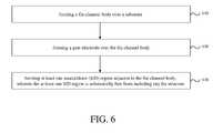
- FIG. 6is a schematic drawing illustrating an exemplary method of forming an exemplary FinFET.
- a conventional FinFET deviceis fabricated using a silicon fin raised from the semiconductor substrate.
- the channel of the deviceis formed in the fin, and a gate is provided over (e.g., surrounding) the fin—for example, in contact with the top and the sidewalls of the fin.
- the gate surrounding the channele.g., fin
- Source/drain regionsare formed at two ends of the fin.
- first and second featuresare formed in direct contact
- additional featuresmay be formed between the first and second features, such that the first and second features may not be in direct contact
- present disclosuremay repeat reference numerals and/or letters in the various examples. This repetition is for the purpose of simplicity and clarity and does not in itself dictate a relationship between the various embodiments and/or configurations discussed.
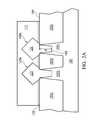
- FIG. 1is a schematic drawing illustrating a top view of an exemplary FinFET of an integrated circuit.
- an integrated circuit 100can include at least one FinFET, e.g., FinFETs 105 a and 105 b .
- Each of the FinFETs 105 a and 105 bcan include a fin-channel body, e.g., fin-channel bodies 110 a and 110 b , respectively, over a substrate 101 .
- a gate electrode 115can be disposed over the fin-channel bodies 110 a and 110 b .
- At least one source/drain (S/D) regione.g., S/D regions 120 a - 120 b and 125 a - 125 b , disposed adjacent to the fin-channel bodies 110 a and 110 b , respectively. At least one of the S/D regions 120 a and 120 b is substantially free from including any fin structure.
- S/Dsource/drain
- the fin-channel bodies 110 a and 110 bare below the gate electrode 115 .
- the fin-channel bodies 110 a and 110 bcannot be seen from the top view of the FinFET 105 and 105 b .
- the fin-channel bodies 110 a and 110 bare represented with dot lines in FIG. 1 to show their locations in the FinFET 105 a and 105 b.
- the fin-channel body 110 acan mean a body that has a fin structure and is merely used for providing a channel between the S/D regions 120 a and 120 b .
- the fin-channel body 110 acan include a fin body that is merely covered by the gate electrode 115 .
- the fin-channel body 110 acan include a fin body that is merely covered by the gate electrode 115 and spacers 107 a and 107 b on sidewalls of the gate electrode 115 .
- the substrate 101may include an elementary semiconductor including silicon or germanium in crystal, polycrystalline, or an amorphous structure; a compound semiconductor including silicon carbide, gallium arsenic, gallium phosphide, indium phosphide, indium arsenide, or indium antimonide; an alloy semiconductor including SiGe, GaAsP, AlInAs, AlGaAs, GaInAs, GaInP, or GaInAsP; any other suitable material; or combinations thereof.
- the alloy semiconductor substratemay have a gradient SiGe feature in which the Si and Ge composition change from one ratio at one location to another ratio at another location of the gradient SiGe feature.
- the alloy SiGeis formed over a silicon substrate.
- a SiGe substrateis strained.
- the semiconductor substratemay be a semiconductor on insulator, such as a silicon on insulator (SOI), or a thin film transistor (TFT).
- SOIsilicon on insulator
- TFTthin film transistor
- the semiconductor substratemay include a doped epi layer or a buried layer.
- the compound semiconductor substratemay have a multilayer structure, or the substrate may include a multilayer compound semiconductor structure.
- an isolation structure 103can include at least one isolation region, e.g., isolation regions 103 a - 103 c .
- the isolation structure 103can be disposed around the FinFETs 105 a and 105 b and electrically isolate the FinFET 105 a from the FinFET 105 b .
- the isolation structure 103can include a shallow trench isolation (STI) structure, a local oxidation of silicon (LOCOS) structure, other isolation structure, or any combination thereof.
- STIshallow trench isolation
- LOClocal oxidation of silicon
- the spacers 107 a and 107 bcan be disposed adjacent to the gate electrode 115 .
- the spacers 107 a and 107 bcan desirably space the S/D regions 120 a , 120 b , 125 a , and 125 b from the gate electrode 115 .
- Each of the spacers 107 a and 107 bcan include at least one material such as oxide, nitride, oxynitride, other dielectric material, or any combinations thereof.
- FIG. 2Ais a schematic cross-sectional view of the integrated circuit 100 shown in FIG. 1 taken along section line 2 A- 2 A.
- the substrate 101can include at least one portion, e.g., portions 102 a and 102 b .
- the portion 102 acan be disposed between the isolation regions 103 a and 103 b .
- a gate dielectric 130can be disposed below the gate electrode 115 .
- the fin-channel bodies 110 a and 110 b(shown in FIG. 1 ) are behind and blocked by the S/D regions 120 a and 125 a , respectively.
- the gate dielectric 130can be a single layer or a multi-layer structure. In some embodiments for multi-layer structures, the gate dielectric 130 can include an interfacial layer and a high-k dielectric layer.
- the interfacial layercan include dielectric material such as, silicon oxide, silicon nitride, silicon oxinitride, other dielectric material, and/or the combinations thereof.
- the high-k dielectric layercan include high-k dielectric materials such as HfO 2 , HfSiO, HfSiON, HfTaO, HfTiO, HfZrO, other suitable high-k dielectric materials, and/or combinations thereof.
- the high-k materialmay further be selected from metal oxides, metal nitrides, metal silicates, transition metal-oxides, transition metal-nitrides, transition metal-silicates, oxynitrides of metals, metal aluminates, zirconium silicate, zirconium aluminate, silicon oxide, silicon nitride, silicon oxynitride, zirconium oxide, titanium oxide, aluminum oxide, hafnium dioxide-alumina alloy, other suitable materials, and/or combinations thereof.
- the gate electrode 115can include polysilicon, silicon-germanium, a metallic material including metal compounds such as, Al, Mo, Cu, W, Ti, Ta, TiN, TaN, NiSi, CoSi, other suitable conductive materials known in the art, or any combination thereof.
- the gate electrode 115can include a polysilicon layer over a metallic layer.
- the gate electrode 115can include a work function metal layer such that it provides an N-metal work function or P-metal work function of a metal gate.
- P-type work function materialsinclude compositions such as ruthenium, palladium, platinum, cobalt, nickel, and conductive metal oxides, and/or other suitable materials.
- N-type metal materialsinclude compositions such as hafnium, zirconium, titanium, tantalum, aluminum, metal carbides (e.g., hafnium carbide, zirconium carbide, titanium carbide, aluminum carbide), aluminides, and/or other suitable materials.
- each of the S/D regions 120 a and 125 acan include an epitaxially-grown region, e.g., epitaxially-grown regions 121 and 123 , respectively.
- the epitaxially-grown region 121can be disposed over the portion 102 a of the substrate 101 .
- the epitaxially-grown region 121 and the portion 102 acan have an interface 104 .
- a central region of the interface 104can be substantially level with a surface 106 of the isolation region 103 a .
- the central region of the interface 104can be below the surface 106 of the isolation region 103 a .
- the central region of the interface 104can be spaced from the surface 106 of the isolation region 103 a by a distance “d”.
- the central region of the interface 104can be substantially flat.
- the epitaxially-grown regions 121 and 123can include dopants.
- the epitaxially-grown regions 121 and 123can have dopants such as Arsenic (As), Phosphorus (P), other group V element, or any combinations thereof.
- the epitaxially-grown regions 121 and 123can have dopants such as boron (B), other group III element, or any combinations thereof.
- the epitaxially-grown region 121 and 123can include a multi-layer structure, e.g., a bi-layer or tri-layer structure.
- a bi-layer structurecan include a SiGe layer below a Si cap layer.
- the FinFET 105 acan include a silicide structure (not shown) disposed over the epitaxially-grown regions 121 and 123 .
- the silicide structuremay comprise materials such as nickel silicide (NiSi), nickel-platinum silicide (NiPtSi), nickel-platinum-germanium silicide (NiPtGeSi), nickel-germanium silicide (NiGeSi), ytterbium silicide (YbSi), platinum silicide (PtSi), iridium silicide (IrSi), erbium silicide (ErSi), cobalt silicide (CoSi), other suitable materials, and/or combinations thereof.
- NiSinickel silicide
- NiPtSinickel-platinum silicide
- NiPtGeSinickel-platinum-germanium silicide
- NiGeSinickel-germanium silicide
- YbSiy
- FIG. 2Bis a schematic cross-sectional view of the integrated circuit 100 shown in FIG. 1 taken along section line 2 B- 2 B.
- the substrate 101can include at least one portion, e.g., portions 102 c and 102 d .
- the fin-channel body 110 acan be disposed over the portion 102 c .
- the fin-channel body 110 acan have a height “h”.
- the portion 102 ccan be disposed between the isolation regions 103 a and 103 b .
- the portion 102 ccan be in connection with the portion 102 a (shown in FIG. 2A ).
- the fin-channel body 110 a and the portion 102 ccan have the same material, e.g., silicon.
- the fin-channel body 110 a and the portion 102 ccan have different materials, e.g., SiGe and Si, respectively.
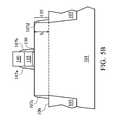
- FIG. 2Cis a schematic cross-sectional view of the integrated circuit 100 shown in FIG. 1 taken along section line 2 C- 2 C.
- the epitaxially-grown regions 121 and 123can be disposed over the portions 102 a and 102 e , respectively, of the substrate 101 .
- the fin-channel body 110 acan be disposed over the portion 102 c of the substrate 101 .
- the interface 104 and the surface 106 of the isolation 103can have a distance “d”.
- the fin-channel body 110 acan have a height “h”.
- a ratio (d/h) of the distance “d” to the height “h”can be about 10 or less. In at least one embodiment, the ratio (d/h) is about 1.
- the epitaxially-grown regions 121 and 123can provide a stress, e.g., compressive stress or tensile stress, to the fin-channel body 110 a .
- the compressed or tensed fin-channel body 110 acan provide a desired electron mobility or hole mobility for the FinFET 105 a .
- the fin-channel body 110 acan have a Si material and the epitaxially-grown regions 121 and 123 can have a SiGe material.
- the fin-channel body 110 a and the epitaxially-grown regions 121 and 123can have a SiGe material.
- the epitaxially-grown regions 121 and 123can have a germanium concentration higher than that of the fin-channel body 110 a.
- the fin-channel body 110 acan have a Si material and the epitaxially-grown regions 121 and 123 can have a SiC material. In other embodiments providing a tensile stress, the fin-channel body 110 a and the epitaxially-grown regions 121 and 123 can have a SiC material. The epitaxially-grown regions 121 and 123 can have a carbon concentration higher than that of the fin-channel body 110 a.
- FIG. 3is a schematic drawing illustrating a simulation result of stress vs. distance (d) of an exemplary FinFET according to some embodiments.
- the vertical axisrepresents a stress applied to a fin-channel body and the horizontal axis represents the distance “d”.
- the fin-channel body 110 ahas a height “h” of about 40 nm and has a Si material.
- the epitaxially-grown regions 121 and 123can have a SiGe material having a germanium concentration of about 36 atomic %.
- An epitaxial silicon layer(not shown) is formed on each of the epitaxially-grown regions 121 and 123 .
- the curve Arepresents that the FinFET 105 a is formed by a gate-first process.
- the curve Brepresents that the FinFET 105 a is formed by a gate-last process.
- the distance “d”is about 0.
- the central region of the interface 104is substantially level with the surface 106 of the isolation region 103 a .
- the stresses of about ⁇ 400 Mpa and ⁇ 700 Mpacan be applied to the fin-channel body 110 a for the FinFET 105 a formed by a gate-first process and a gate-last process, respectively.
- the stressis increased for the fin-channel body 110 a of the FinFET 105 a formed by a gate-first process or a gate-last process (as indicated by arrows A and B).
- the increase of the stress applied to the fin-channel body 110 a for the FinFET 105 acan become slow.
- the epitaxially-grown regions 121 and 123are free from including any fin structure. The amount of the epitaxially-grown regions 121 and 123 can provide a desired stress to the fin-channel body 110 a for the FinFET 105 a.
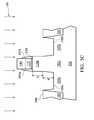
- FIG. 4is an enlarged schematic cross-sectional view of another exemplary FinFET including a portion of the substrate and isolation regions. Items of FIG. 4 that are the same items in FIG. 2A are indicated by the same reference numerals, increased by 300.
- an isolation region 403 acan have a corner 408 where a surface 406 of the isolation region 403 a and an interface 409 between the isolation region 403 a and the portion 402 a of the substrate 401 intersect.
- the portion 402 a of the substrate 401can have a tip 411 where a surface 404 of the portion 402 a of the substrate 401 and the interface 409 between the isolation region 403 a and the portion 402 a of the substrate 401 intersect.
- a process for forming the epitaxially-grown region 421can include a reflow process in a hydrogen-containing ambient.
- the reflow processcan flat the central portion of the surface 404 .
- a desired amount of the epitaxially-grown region 421can be formed from the portion 402 a of the substrate 401 .
- the desired amount of the epitaxially-grown region 421can provide a stress to the fin-channel body for the FinFET.
- the amount of the epitaxially-grown region 421may also reduce resistances of the source/drain regions.
- dopants added in the epitaxially-grown region 421 by an in-situ processcan further reduce the resistances of the source/drain regions.
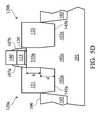
- FIGS. 5A-5Dare schematic cross-sectional views illustrating an exemplary method for forming the FinFET shown in FIG. 1 taken along section line 2 C- 2 C.
- the isolation structure 103can be formed within and/or over the substrate 101 .
- a fin 135can be formed over the substrate 101 .
- the fin 135can have a height “h”.
- the gate dielectric 130 and the gate electrode 115can be formed over the fin 135 .
- a hard-mask layer 140can be formed over the gate electrode 115 .
- a spacer layer 107can be formed substantially conformal over the fin 135 , the hard-mask layer 140 , and sidewalls of the gate electrode 115 and the gate dielectric 130 .
- the isolation structure 103 , the gate dielectric 130 , the gate electrode 115 , the spacer layer 107 , the fin 135 , and/or the hard-mask layer 140can be formed by processes including, for example, deposition process, etch processes, clean process, lithographic process, and/or any combinations thereof.
- portions of the spacer layer 107can be removed for forming the spacers 107 a - 107 d .
- the spacers 107 a and 107 bcan be formed on the sidewalls of the gate electrode 115 .
- Spacers 107 c and 107 dcan be formed on the sidewalls of the fin 135 .
- the spacers 107 a and 107 bcan cover the gate electrode 115 to avoid a mushroom effect resulting from an epitaxy-growth from the sidewalls of the gate electrode 115 .
- the isolation structure 103 , the gate dielectric 130 , the gate electrode 115 , the spacers 107 a and 107 b , the fin 135 , and/or the hard-mask layer 140can be formed by processes including, for example, deposition process, etch processes, clean process, lithographic process, and/or any combinations thereof.
- a removing process 145can remove at least a portion of the fin 135 to expose the surfaces 145 a of the portion 102 a and 145 b of the portion 102 e of the substrate 101 and to define the fin-channel body 110 a .
- the removing process 145can also remove the spacers 107 c and 107 d .
- the removing process 145can substantially remove the portion of the fin 135 such that a central region of the exposed surface 145 a can be substantially level with the surface 106 of the isolation structure 103 .
- the removing process 145can remove a portion of the substrate 101 such that the central region of the exposed surface 145 a can be below the surface 106 of the isolation structure 103 .
- the distance “d”can be defined between the exposed surface 145 a and the surface 106 of the isolation structure 103 .
- a ratio (d/h) of the distance “d” to the height “h”can be about 10 or less. In at least one embodiment, the ratio (d/h) can be about 1.
- the process steps described above in conjunction with FIGS. 5A-5Ccan be referred to as processes of forming the fin-channel body 145 a over the substrate 101 and forming the gate electrode 115 over the fin-channel body 145 a (processes 610 and 620 shown in FIG. 6 ).
- the process 610can include one or more known semiconductor processing steps for forming the fin-channel body 145 a .
- one or more step described above in conjunction with FIGS. 5A-5Ccan be saved for performing the processes 610 and 620 .
- At least one source/drain (S/D) regione.g., the S/D regions 120 a and 120 b can be formed adjacent to the fin-channel body 110 a .
- forming the S/D regions 120 a and 120 bcan include epitaxially growing the epitaxially grown-regions 121 and 123 , respectively, from the exposed surface 145 a of the portion 102 a and the exposed surface 145 b of the portion 102 e of the substrate 101 .
- each of the epitaxially grown-regions 121 and 123can have a (1 0 0) facet.
- the process steps described above in conjunction with FIG. 5A-5Dcan be referred to as a process of forming at least one source/drain (S/D) region adjacent to the fin-channel body, wherein the at least one S/D region is substantially free from including any fin structure (process 630 shown in FIG. 6 ).
- S/Dsource/drain
- the method for forming the FinFET 100can include implanting dopants within the S/D regions 120 a and 120 b .
- the S/D regions 120 a and 120 bcan have dopants such as Arsenic (As), Phosphorus (P), other group V element, or the combinations thereof.
- the method for forming the FinFET 100can include salicidating at least a portion of the epitaxially-grown regions 121 and 123 .
- the silicide of the epitaxially-grown regions 121 and 123can provide a desired conductivity.
- the silicidemay comprise materials such as nickel silicide (NiSi), nickel-platinum silicide (NiPtSi), nickel-platinum-germanium silicide (NiPtGeSi), nickel-germanium silicide (NiGeSi), ytterbium silicide (YbSi), platinum silicide (PtSi), iridium silicide (IrSi), erbium silicide (ErSi), cobalt silicide (CoSi), other suitable materials, and/or combinations thereof.
- NiSinickel silicide
- NiPtSinickel-platinum silicide
- NiPtGeSinickel-platinum-germanium silicide
- NiGeSinickel-germanium silicide
- YbSiytterbium silicide
- IrSiiridium silicide
- ErSierbium si
- the materials utilized to create the silicidemay be deposited using PVD such as sputtering and evaporation; plating; CVD such as plasma enhanced CVD (PECVD), atmospheric pressure CVD (APCVD), low pressure CVD (LPCVD), high density plasma CVD (HDPCVD) and atomic layer CVD (ALCVD); other suitable deposition processes; and/or combinations thereof.
- PECVDplasma enhanced CVD
- APCVDatmospheric pressure CVD
- LPCVDlow pressure CVD
- HDPCVDhigh density plasma CVD
- ACVDatomic layer CVD
- the salicidation processmay continue with a reaction between the deposited material and the doped regions at an elevated temperature that is selected based on the specific material or materials. This is also referred to as annealing, which may include a Rapid Thermal Process (RTP).
- RTPRapid Thermal Process
- the reacted silicidemay require a one step RTP or multiple step RTPs.
- the method for forming the FinFET 100can include forming an epitaxial layer (not shown), e.g., a silicon epitaxial layer, over each of the epitaxially-grown regions 121 and 123 .
- the methodcan include salicidating at least a portion of the epitaxial layer. It is found that the silicide formed from the silicon epitaxial layer can desirably reduce defects of the silicide. A desired conductivity of the silicide can be reached.
- the method for forming the FinFET 100can include an etch process (not shown) for removing a portion of the substrate 101 .
- the etch processcan include, for example, a dry etch, a wet etch, and/or any combinations thereof.
- the etch processcan be performed after the removing process 145 described above in conjunction with FIG. 2B and/or before the forming the epitaxially-grown regions 121 and 123 described above in conjunction with FIG. 2C .
- a top corner of the isolation structure 103may be higher than a tip of the portion 102 a of the substrate 101 .
- the etch processcan remove the portion of the substrate 101 such that a corner of the isolation structure 103 is substantially adjacent to a tip of the portion 102 a of the substrate 101 as described above in conjunction with FIG. 4 .
- the substantially-leveled corner and tipcan let a desired amount of the epitaxially-grown regions 121 and 123 formed from the exposed surfaces 145 a and 145 b , respectively.
- the desired amount of the epitaxially-grown regions 121 and 123can provide a desired stress to the fin-channel body 110 a.
- the method for forming the FinFET 100can include reflowing the exposed surfaces 145 a and 145 b of the substrate 101 such that the central region of the exposed surfaces 145 a and 145 b of the substrate are substantially flat.
- the substantially flat central regions of the exposed surfaces 145 a and 145 bcan let the epitaxially-grown regions 121 and 123 desirably formed from the exposed surfaces 145 a and 145 b , respectively.
- reflowing the exposed surfaces 145 a and 145 bcan be performed in a hydrogen-containing ambient and at a processing temperature between about 600° C. and about 800° C. for about 30 minutes.
- At least one dielectric structurecan be formed over the substrate.
- the dielectric structuremay include materials such as oxide, nitride, oxynitride, low-k dielectric material, ultra low-k dielectric material, or any combinations thereof.
- the dielectric structuremay be formed by, for example, a CVD process, a HDP CVD process, a HARP, a spin-coating process, other deposition process, and/or any combinations thereof.
- contact plugs, via plugs, metallic regions, and/or metallic linescan be formed within the dielectric structure for interconnection.
- the contact plugs, via plugs, metallic regions, and/or metallic linescan include materials such as tungsten, aluminum, copper, titanium, tantalum, titanium nitride, tantalum nitride, nickel silicide, cobalt silicide, other proper conductive materials, and/or combinations thereof.
- the contact plugs, via plugs, metallic regions, and/or metallic linescan be formed by any suitable processes, such as deposition, photolithography, and etching processes, and/or combinations thereof. It is noted that the method described above in conjunction with FIGS. 5A-5D are merely exemplary. The method can be a gate-first process or a gate-last process. The scope of the invention is not limited thereto.
- the FinFETs 105 a and/or 105 bcan be formed within a package which can be physically and electrically coupled with a printed wiring board or printed circuit board (PCB) to form an electronic assembly.
- the electronic assemblycan be part of an electronic system such as computers, wireless communication devices, computer-related peripherals, entertainment devices, or the like.
- the system including the integrated circuit 100can provides an entire system in one IC, so-called system on a chip (SOC) or system on integrated circuit (SOIC) devices.
- SOC devicesmay provide, for example, all of the circuitry needed to implement a cell phone, personal data assistant (PDA), digital VCR, digital camcorder, digital camera, MP3 player, or the like in a single integrated circuit.
- PDApersonal data assistant
- VCRdigital VCR
- digital camcorderdigital camera
- MP3 playeror the like in a single integrated circuit.
Landscapes
- Insulated Gate Type Field-Effect Transistor (AREA)
- Electrodes Of Semiconductors (AREA)
- Thin Film Transistor (AREA)
- Metal-Oxide And Bipolar Metal-Oxide Semiconductor Integrated Circuits (AREA)
Abstract
Description
The present application claims priority of U.S. Application Ser. No. 61/247,756, filed on Oct. 1, 2009, which is incorporated herein by reference in its entirety.
The present application is related to U.S. patent application Ser. No. 12/707,788, filed on Feb. 18, 2010, titled MEMORY POWER GATING CIRCUIT AND METHODS; Ser. No. 12/758,426, filed on Apr. 12, 2010, titled FINFETS AND METHODS FOR FORMING THE SAME; Ser. No. 12/731,325, filed on Mar. 25, 2010, titled ELECTRICAL FUSE AND RELATED APPLICATIONS; Ser. No. 12/724,556, filed on Mar. 16, 2010, titled ELECTRICAL ANTI-FUSE AND RELATED APPLICATIONS; Ser. No. 12/757,203, filed on Apr. 9, 2010, titled STI STRUCTURE AND METHOD OF FORMING BOTTOM VOID IN SAME; Ser. No. 12/797,839, filed on Jun. 10, 2010, titled FIN STRUCTURE FOR HIGH MOBILITY MULTIPLE-GATE TRANSISTOR; Ser. No. 12/831,842, filed on Jul. 7, 2010, titled METHOD FOR FORMING HIGH GERMANIUM CONCENTRATION SiGe STRESSOR; Ser. No. 12/761,686, filed on Apr. 16, 2010, titled FIN FIELD EFFECT TRANSISTOR; Ser. No. 12/757,271, filed on Apr. 9, 2010, titled ACCUMULATION TYPE FINFET, CIRCUITS AND FABRICATION METHOD THEREOF; Ser. No. 12/694,846, filed on Jan. 27, 2010, titled INTEGRATED CIRCUITS AND METHODS FOR FORMING THE SAME; Ser. No. 12/638,958, filed on Dec. 14, 2009, titled METHOD OF CONTROLLING GATE THICKNESS IN FORMING FINFET DEVICES; Ser. No. 12/768,884, filed on Apr. 28, 2010, titled METHODS FOR DOPING FIN FIELD-EFFECT TRANSISTORS; Ser. No. 12/731,411, filed on Mar. 25, 2010, titled INTEGRATED CIRCUIT INCLUDING FINFETS AND METHODS FOR FORMING THE SAME; Ser. No. 12/775,006, filed on May 6, 2010, titled METHOD FOR FABRICATING A STRAINED STRUCTURE; Ser. No. 12/886,713, filed Sep. 21, 2010, titled METHOD OF FORMING INTEGRATED CIRCUITS; Ser. No. 12/941,509, filed Nov. 8, 2010, titled MECHANISMS FOR FORMING ULTRA SHALLOW JUNCTION; Ser. No. 12/900,626, filed Oct. 8, 2010, titled TRANSISTOR HAVING NOTCHED FIN STRUCTURE AND METHOD OF MAKING THE SAME; Ser. No. 12/903,712, filed Oct. 13, 2010, titled FINFET AND METHOD OF FABRICATING THE SAME; 61/412,846, filed Nov. 12, 2010, 61/394,418, filed Oct. 19, 2010, titled METHODS OF FORMING GATE DIELECTRIC MATERIAL; 61/405,858, filed Oct. 22, 2010, titled METHODS OF FORMING SEMICONDUCTOR DEVICES; and Ser. No. 12/267,121, filed Nov. 7, 2008, titled FINFET PROCESS COMPATIBLE NATIVE TRANSISTOR.
The present application relates generally to the field of semiconductor devices, and more particularly, to Fin field effect transistors (FinFETs) and methods for forming the FinFETs.
The semiconductor integrated circuit (IC) industry has experienced rapid growth. Technological advances in IC materials and design have produced generations of ICs where each generation has smaller and more complex circuits than the previous generation. For example, the semiconductor industry ardently strives to decrease the size of memory cells. One strategy that has been employed includes the use of multiple gate transistors, otherwise known as FinFETs.
The present disclosure is best understood from the following detailed description when read with the accompanying figures. It is emphasized that, in accordance with the standard practice in the industry, various features are not drawn to scale and are used for illustration purposes only. In fact, the dimensions of the various features may be arbitrarily increased or reduced for clarity of discussion.
A conventional FinFET device is fabricated using a silicon fin raised from the semiconductor substrate. The channel of the device is formed in the fin, and a gate is provided over (e.g., surrounding) the fin—for example, in contact with the top and the sidewalls of the fin. The gate surrounding the channel (e.g., fin) is beneficial in that allows control of the channel from three sides. Source/drain regions are formed at two ends of the fin.
It is understood that the following disclosure provides many different embodiments, or examples, for implementing different features of the invention. Specific examples of components and arrangements are described below to simplify the present disclosure. These are, of course, merely examples and are not intended to be limiting. For example, the formation of a first feature over or on a second feature in the description that follows may include embodiments in which the first and second features are formed in direct contact, and may also include embodiments in which additional features may be formed between the first and second features, such that the first and second features may not be in direct contact. In addition, the present disclosure may repeat reference numerals and/or letters in the various examples. This repetition is for the purpose of simplicity and clarity and does not in itself dictate a relationship between the various embodiments and/or configurations discussed.
It is noted the fin-channel bodies gate electrode 115. The fin-channel bodies channel bodies FIG. 1 to show their locations in theFinFET
In some embodiments, the fin-channel body 110acan mean a body that has a fin structure and is merely used for providing a channel between the S/D regions channel body 110acan include a fin body that is merely covered by thegate electrode 115. In still other embodiments, the fin-channel body 110acan include a fin body that is merely covered by thegate electrode 115 andspacers gate electrode 115.
In some embodiments, thesubstrate 101 may include an elementary semiconductor including silicon or germanium in crystal, polycrystalline, or an amorphous structure; a compound semiconductor including silicon carbide, gallium arsenic, gallium phosphide, indium phosphide, indium arsenide, or indium antimonide; an alloy semiconductor including SiGe, GaAsP, AlInAs, AlGaAs, GaInAs, GaInP, or GaInAsP; any other suitable material; or combinations thereof. In one embodiment, the alloy semiconductor substrate may have a gradient SiGe feature in which the Si and Ge composition change from one ratio at one location to another ratio at another location of the gradient SiGe feature. In another embodiment, the alloy SiGe is formed over a silicon substrate. In yet another embodiment, a SiGe substrate is strained. Furthermore, the semiconductor substrate may be a semiconductor on insulator, such as a silicon on insulator (SOI), or a thin film transistor (TFT). In some examples, the semiconductor substrate may include a doped epi layer or a buried layer. In other examples, the compound semiconductor substrate may have a multilayer structure, or the substrate may include a multilayer compound semiconductor structure.
Referring toFIG. 1 , anisolation structure 103 can include at least one isolation region, e.g.,isolation regions 103a-103c. Theisolation structure 103 can be disposed around theFinFETs FinFET 105afrom theFinFET 105b. Theisolation structure 103 can include a shallow trench isolation (STI) structure, a local oxidation of silicon (LOCOS) structure, other isolation structure, or any combination thereof.
Referring toFIG. 1 , thespacers gate electrode 115. Thespacers D regions gate electrode 115. Each of thespacers
In some embodiments, thegate dielectric 130 can be a single layer or a multi-layer structure. In some embodiments for multi-layer structures, thegate dielectric 130 can include an interfacial layer and a high-k dielectric layer. The interfacial layer can include dielectric material such as, silicon oxide, silicon nitride, silicon oxinitride, other dielectric material, and/or the combinations thereof. The high-k dielectric layer can include high-k dielectric materials such as HfO2, HfSiO, HfSiON, HfTaO, HfTiO, HfZrO, other suitable high-k dielectric materials, and/or combinations thereof. The high-k material may further be selected from metal oxides, metal nitrides, metal silicates, transition metal-oxides, transition metal-nitrides, transition metal-silicates, oxynitrides of metals, metal aluminates, zirconium silicate, zirconium aluminate, silicon oxide, silicon nitride, silicon oxynitride, zirconium oxide, titanium oxide, aluminum oxide, hafnium dioxide-alumina alloy, other suitable materials, and/or combinations thereof.
In some embodiments, thegate electrode 115 can include polysilicon, silicon-germanium, a metallic material including metal compounds such as, Al, Mo, Cu, W, Ti, Ta, TiN, TaN, NiSi, CoSi, other suitable conductive materials known in the art, or any combination thereof. In other embodiments, thegate electrode 115 can include a polysilicon layer over a metallic layer. In still other embodiments, thegate electrode 115 can include a work function metal layer such that it provides an N-metal work function or P-metal work function of a metal gate. P-type work function materials include compositions such as ruthenium, palladium, platinum, cobalt, nickel, and conductive metal oxides, and/or other suitable materials. N-type metal materials include compositions such as hafnium, zirconium, titanium, tantalum, aluminum, metal carbides (e.g., hafnium carbide, zirconium carbide, titanium carbide, aluminum carbide), aluminides, and/or other suitable materials.
In some embodiments, each of the S/D regions regions region 121 can be disposed over theportion 102aof thesubstrate 101. The epitaxially-grownregion 121 and theportion 102acan have aninterface 104. In some embodiments, a central region of theinterface 104 can be substantially level with asurface 106 of theisolation region 103a. In other embodiments, the central region of theinterface 104 can be below thesurface 106 of theisolation region 103a. In still other embodiments, the central region of theinterface 104 can be spaced from thesurface 106 of theisolation region 103aby a distance “d”. In still other embodiments, the central region of theinterface 104 can be substantially flat.
In some embodiments, the epitaxially-grownregions regions regions region
In some embodiments, theFinFET 105acan include a silicide structure (not shown) disposed over the epitaxially-grownregions
Referring toFIG. 2C , the epitaxially-grownregions channel body 110a. The compressed or tensed fin-channel body 110acan provide a desired electron mobility or hole mobility for theFinFET 105a. In some embodiments providing a compressive stress, the fin-channel body 110acan have a Si material and the epitaxially-grownregions channel body 110aand the epitaxially-grownregions regions channel body 110a.
In some embodiments providing a tensile stress, the fin-channel body 110acan have a Si material and the epitaxially-grownregions channel body 110aand the epitaxially-grownregions regions channel body 110a.
Referring again toFIG. 3 , in some embodiments the distance “d” is about 0. The central region of theinterface 104 is substantially level with thesurface 106 of theisolation region 103a. The stresses of about −400 Mpa and −700 Mpa can be applied to the fin-channel body 110afor theFinFET 105aformed by a gate-first process and a gate-last process, respectively. By increasing the distances “d”, the stress is increased for the fin-channel body 110aof theFinFET 105aformed by a gate-first process or a gate-last process (as indicated by arrows A and B). In other embodiments, if the distance “d” is substantially equal to or larger than the height “h”, the increase of the stress applied to the fin-channel body 110afor theFinFET 105acan become slow. From the foregoing, the epitaxially-grownregions regions channel body 110afor theFinFET 105a.
It is found that if thecorner 408 is substantially adjacent to thetip 411, a desired amount of the epitaxially-grownregion 421 can be formed from theportion 402aof thesubstrate 401. The desired amount of the epitaxially-grownregion 421 can provide a stress to the fin-channel body for the FinFET. The amount of the epitaxially-grownregion 421 may also reduce resistances of the source/drain regions. In some embodiments, dopants added in the epitaxially-grownregion 421 by an in-situ process can further reduce the resistances of the source/drain regions.
Referring toFIG. 5B , portions of the spacer layer107 (shown inFIG. 5A ) can be removed for forming thespacers 107a-107d. Thespacers gate electrode 115.Spacers fin 135. In some embodiments, thespacers gate electrode 115 to avoid a mushroom effect resulting from an epitaxy-growth from the sidewalls of thegate electrode 115. Theisolation structure 103, thegate dielectric 130, thegate electrode 115, thespacers fin 135, and/or the hard-mask layer 140 can be formed by processes including, for example, deposition process, etch processes, clean process, lithographic process, and/or any combinations thereof.
ReferringFIG. 5C , a removingprocess 145 can remove at least a portion of thefin 135 to expose thesurfaces 145aof theportion portion 102eof thesubstrate 101 and to define the fin-channel body 110a. The removingprocess 145 can also remove thespacers process 145 can substantially remove the portion of thefin 135 such that a central region of the exposedsurface 145acan be substantially level with thesurface 106 of theisolation structure 103. In other embodiments, the removingprocess 145 can remove a portion of thesubstrate 101 such that the central region of the exposedsurface 145acan be below thesurface 106 of theisolation structure 103. The distance “d” can be defined between the exposedsurface 145aand thesurface 106 of theisolation structure 103. A ratio (d/h) of the distance “d” to the height “h” can be about 10 or less. In at least one embodiment, the ratio (d/h) can be about 1.
In some embodiments, the process steps described above in conjunction withFIGS. 5A-5C can be referred to as processes of forming the fin-channel body 145aover thesubstrate 101 and forming thegate electrode 115 over the fin-channel body 145a(processes610 and620 shown inFIG. 6 ). In other embodiments, theprocess 610 can include one or more known semiconductor processing steps for forming the fin-channel body 145a. In still other embodiments, one or more step described above in conjunction withFIGS. 5A-5C can be saved for performing theprocesses
Referring toFIG. 5D , at least one source/drain (S/D) region, e.g., the S/D regions channel body 110a. In some embodiments, forming the S/D regions regions surface 145aof theportion 102aand the exposedsurface 145bof theportion 102eof thesubstrate 101. In some embodiments, each of the epitaxially grown-regions
In some embodiments, the process steps described above in conjunction withFIG. 5A-5D can be referred to as a process of forming at least one source/drain (S/D) region adjacent to the fin-channel body, wherein the at least one S/D region is substantially free from including any fin structure (process 630 shown inFIG. 6 ).
In some embodiments, the method for forming theFinFET 100 can include implanting dopants within the S/D regions D regions
In other embodiments, the method for forming theFinFET 100 can include salicidating at least a portion of the epitaxially-grownregions regions
In some embodiments, the method for forming theFinFET 100 can include forming an epitaxial layer (not shown), e.g., a silicon epitaxial layer, over each of the epitaxially-grownregions
In other embodiments, the method for forming theFinFET 100 can include an etch process (not shown) for removing a portion of thesubstrate 101. The etch process can include, for example, a dry etch, a wet etch, and/or any combinations thereof. The etch process can be performed after the removingprocess 145 described above in conjunction withFIG. 2B and/or before the forming the epitaxially-grownregions FIG. 2C . In some embodiments, after the removingprocess 145, a top corner of theisolation structure 103 may be higher than a tip of theportion 102aof thesubstrate 101. The etch process can remove the portion of thesubstrate 101 such that a corner of theisolation structure 103 is substantially adjacent to a tip of theportion 102aof thesubstrate 101 as described above in conjunction withFIG. 4 . The substantially-leveled corner and tip can let a desired amount of the epitaxially-grownregions surfaces regions channel body 110a.
In still other embodiments, the method for forming theFinFET 100 can include reflowing the exposedsurfaces substrate 101 such that the central region of the exposedsurfaces surfaces regions surfaces surfaces
In some embodiments, at least one dielectric structure (not shown) can be formed over the substrate. The dielectric structure may include materials such as oxide, nitride, oxynitride, low-k dielectric material, ultra low-k dielectric material, or any combinations thereof. The dielectric structure may be formed by, for example, a CVD process, a HDP CVD process, a HARP, a spin-coating process, other deposition process, and/or any combinations thereof.
In some embodiments, contact plugs, via plugs, metallic regions, and/or metallic lines can be formed within the dielectric structure for interconnection. The contact plugs, via plugs, metallic regions, and/or metallic lines can include materials such as tungsten, aluminum, copper, titanium, tantalum, titanium nitride, tantalum nitride, nickel silicide, cobalt silicide, other proper conductive materials, and/or combinations thereof. The contact plugs, via plugs, metallic regions, and/or metallic lines can be formed by any suitable processes, such as deposition, photolithography, and etching processes, and/or combinations thereof. It is noted that the method described above in conjunction withFIGS. 5A-5D are merely exemplary. The method can be a gate-first process or a gate-last process. The scope of the invention is not limited thereto.
In some embodiments, theFinFETs 105aand/or105bcan be formed within a package which can be physically and electrically coupled with a printed wiring board or printed circuit board (PCB) to form an electronic assembly. The electronic assembly can be part of an electronic system such as computers, wireless communication devices, computer-related peripherals, entertainment devices, or the like.
In some embodiments, the system including the integratedcircuit 100 can provides an entire system in one IC, so-called system on a chip (SOC) or system on integrated circuit (SOIC) devices. These SOC devices may provide, for example, all of the circuitry needed to implement a cell phone, personal data assistant (PDA), digital VCR, digital camcorder, digital camera, MP3 player, or the like in a single integrated circuit.
The foregoing outlines features of several embodiments so that those skilled in the art may better understand the aspects of the present disclosure. Those skilled in the art should appreciate that they may readily use the present disclosure as a basis for designing or modifying other processes and structures for carrying out the same purposes and/or achieving the same advantages of the embodiments introduced herein. Those skilled in the art should also realize that such equivalent constructions do not depart from the spirit and scope of the present disclosure, and that they may make various changes, substitutions, and alterations herein without departing from the spirit and scope of the present disclosure.
Claims (15)
1. A Fin field effect transistor (FinFET) comprising:
a fin-channel body over a substrate;
a gate electrode disposed over the fin-channel body; and
at least one source/drain (S/D) region disposed adjacent to the fin-channel body, the at least one S/D region being substantially free from including any fin structure, wherein
the substrate has a portion between a first isolation region and a second isolation region, the at least one S/D region includes an epitaxially-grown region, and the epitaxially-grown region is disposed over the portion of the substrate, and
the first isolation region has a corner where a surface of the first isolation region and an interface between the first isolation region and the portion of the substrate intersect, the portion of the substrate has a tip where a surface of the portion of the substrate and the interface between the first isolation region and the portion of the substrate intersect, and the corner is substantially adjacent to the tip.
2. The FinFETclaim 1 , wherein the epitaxially-grown region and the portion of the substrate have an interface and a central region of the interface is below a surface of the first isolation region.
3. The FinFET ofclaim 2 , wherein a distance between the central region of the interface and the surface of the first isolation region is substantially equal to a height of the fin-channel body.
4. The FinFET ofclaim 2 , wherein the central region of the interface is substantially flat.
5. The FinFETclaim 1 , wherein the epitaxially-grown region is configured for providing a stress to the fin-channel body.
6. The FinFETclaim 1 , further comprising a silicide structure disposed over the epitaxially-grown region.
7. A Fin field effect transistor (FinFET) comprising:
a fin-channel body over a substrate, the substrate having a portion between a first isolation region and a second isolation region;
a gate electrode disposed over the fin-channel body; and
at least one source/drain (S/D) region disposed adjacent to the fin-channel body, the at least one S/D region comprising:
an epitaxially-grown region disposed over the portion of the substrate, wherein the epitaxially-grown region and the portion of the substrate has an interface and a central region of the interface is below a surface of the first isolation region; and
a silicide structure disposed over the epitaxially-grown region,
wherein the first isolation region has a corner where the surface of the first isolation region and a sidewall of the first isolation region intersect, the portion of the substrate has a tip where a surface of the portion of the substrate and a sidewall of the portion of the substrate intersect, and the corner is substantially adjacent to the tip.
8. The FinFET ofclaim 7 , wherein a distance between the central region of the interface and the surface of the first isolation region is substantially equal to a height of the fin-channel body.
9. The FinFET ofclaim 7 , wherein the central region of the interface is substantially flat.
10. The FinFET ofclaim 7 , wherein the epitaxially-grown region is capable of providing a stress to the fin-channel body.
11. A method for forming a Fin field effect transistor (FinFET), the method comprising:
forming a fin over a substrate, and removing at least one end portion of the fin to expose a surface of a portion of the substrate surrounded by first and second isolation regions to form a fin-channel body over the substrate, wherein the first isolation region has a corner where a surface of the first isolation region and a sidewall of the first isolation region intersect, the portion of the substrate has a tip where a surface of the portion of the substrate and a sidewall of the portion of the substrate intersect, and the corner is substantially adjacent to the tip;
forming a gate electrode over the fin-channel body; and
epitaxially growing at least one S/D region from the exposed surface of the portion of the substrate to form the at least one source/drain (S/D) region adjacent to the fin-channel body, the at least one S/D region being substantially free from including any fin structure.
12. The method ofclaim 11 , further comprising removing a portion of the substrate, wherein a central region of the exposed surface of the portion of the substrate is below a surface of the first isolation region.
13. The method ofclaim 12 , wherein a distance between the central region of the exposed surface of the substrate and the surface of the first isolation region is substantially equal to a height of the fin-channel body.
14. The method ofclaim 12 further comprising reflowing the exposed surface of the substrate such that the central region of the exposed surface of the substrate is substantially flat.
15. The method ofclaim 11 , further comprising:
forming an epitaxial layer over the at least one S/D region; and
salicidating at least one of the epitaxial layer.
Priority Applications (8)
| Application Number | Priority Date | Filing Date | Title |
|---|---|---|---|
| US12/761,686US8264021B2 (en) | 2009-10-01 | 2010-04-16 | Finfets and methods for forming the same |
| US12/766,233US9484462B2 (en) | 2009-09-24 | 2010-04-23 | Fin structure of fin field effect transistor |
| TW099132977ATWI456760B (en) | 2009-10-01 | 2010-09-29 | Fin field effect transistor and forming method thereof |
| KR1020100094454AKR101217327B1 (en) | 2009-10-01 | 2010-09-29 | FinFETS and methods for forming the same |
| CN201010501836.1ACN102034871B (en) | 2009-10-01 | 2010-09-30 | Fin field effect transistor and method of forming the same |
| JP2010221860AJP5595856B2 (en) | 2009-10-01 | 2010-09-30 | FINFETS and method for forming the same |
| US14/102,702US9660082B2 (en) | 2009-07-28 | 2013-12-11 | Integrated circuit transistor structure with high germanium concentration SiGe stressor |
| US15/339,258US10355108B2 (en) | 2009-09-24 | 2016-10-31 | Method of forming a fin field effect transistor comprising two etching steps to define a fin structure |
Applications Claiming Priority (2)
| Application Number | Priority Date | Filing Date | Title |
|---|---|---|---|
| US24775609P | 2009-10-01 | 2009-10-01 | |
| US12/761,686US8264021B2 (en) | 2009-10-01 | 2010-04-16 | Finfets and methods for forming the same |
Publications (2)
| Publication Number | Publication Date |
|---|---|
| US20110079829A1 US20110079829A1 (en) | 2011-04-07 |
| US8264021B2true US8264021B2 (en) | 2012-09-11 |
Family
ID=43822531
Family Applications (1)
| Application Number | Title | Priority Date | Filing Date |
|---|---|---|---|
| US12/761,686Active2030-09-10US8264021B2 (en) | 2009-07-28 | 2010-04-16 | Finfets and methods for forming the same |
Country Status (5)
| Country | Link |
|---|---|
| US (1) | US8264021B2 (en) |
| JP (1) | JP5595856B2 (en) |
| KR (1) | KR101217327B1 (en) |
| CN (1) | CN102034871B (en) |
| TW (1) | TWI456760B (en) |
Cited By (36)
| Publication number | Priority date | Publication date | Assignee | Title |
|---|---|---|---|---|
| US20110278676A1 (en)* | 2010-05-14 | 2011-11-17 | Taiwan Semiconductor Manufacturing Company, Ltd. | Method and apparatus for enhancing channel strain |
| US20120091538A1 (en)* | 2010-10-13 | 2012-04-19 | Taiwan Semiconductor Manufacturing Company, Ltd. | Finfet and method of fabricating the same |
| US20130109152A1 (en)* | 2010-02-09 | 2013-05-02 | Taiwan Semiconductor Manufacturing Co., Ltd. | Method of making lower parasitic capacitance finfet |
| US8679925B2 (en) | 2012-01-03 | 2014-03-25 | Taiwan Semiconductor Manufacturing Company, Ltd. | Methods of manufacturing semiconductor devices and transistors |
| US20140239414A1 (en)* | 2012-01-09 | 2014-08-28 | Taiwan Semiconductor Manufacturing Company, Ltd. | FinFETs and the Methods for Forming the Same |
| US20150024584A1 (en)* | 2013-07-17 | 2015-01-22 | Global Foundries, Inc. | Methods for forming integrated circuits with reduced replacement metal gate height variability |
| US9006066B2 (en) | 2013-04-26 | 2015-04-14 | Globalfoundries Inc. | FinFET with active region shaped structures and channel separation |
| US9034700B1 (en) | 2013-11-21 | 2015-05-19 | Samsung Electronics Co., Ltd. | Integrated circuit devices including finFETs and methods of forming the same |
| US20150214331A1 (en)* | 2014-01-30 | 2015-07-30 | Globalfoundries Inc. | Replacement metal gate including dielectric gate material |
| US9123633B2 (en) | 2013-02-01 | 2015-09-01 | Taiwan Semiconductor Manufacturing Company, Ltd. | Methods for forming semiconductor regions in trenches |
| US9293587B2 (en) | 2013-07-23 | 2016-03-22 | Globalfoundries Inc. | Forming embedded source and drain regions to prevent bottom leakage in a dielectrically isolated fin field effect transistor (FinFET) device |
| US9299811B2 (en) | 2013-11-27 | 2016-03-29 | Samsung Electronics Co., Ltd. | Methods of fabricating semiconductor devices |
| US9337031B2 (en) | 2014-01-28 | 2016-05-10 | Samsung Electronics Co., Ltd. | Semiconductor devices and methods of manufacturing the same |
| US9349798B1 (en) | 2015-06-29 | 2016-05-24 | International Business Machines Corporation | CMOS structures with selective tensile strained NFET fins and relaxed PFET fins |
| US9368388B2 (en) | 2012-04-13 | 2016-06-14 | Taiwan Semiconductor Manufacturing Company, Ltd. | Apparatus for FinFETs |
| US9379107B2 (en) | 2014-04-22 | 2016-06-28 | Samsung Electronics Co., Ltd. | FinFET semiconductor devices including dummy structures |
| US9397219B2 (en) | 2014-07-25 | 2016-07-19 | Samsung Electronics Co., Ltd. | Semiconductor devices having source/drain regions with strain-inducing layers and methods of manufacturing such semiconductor devices |
| US9466724B2 (en) | 2014-09-29 | 2016-10-11 | Samsung Electronics Co., Ltd. | Semiconductor devices having source/drain and method of fabricating the same |
| US9472470B2 (en) | 2014-12-09 | 2016-10-18 | GlobalFoundries, Inc. | Methods of forming FinFET with wide unmerged source drain EPI |
| US9536881B2 (en) | 2013-04-23 | 2017-01-03 | Samsung Electronics Co., Ltd. | Semiconductor devices having fin shaped channels |
| US9543167B2 (en) | 2014-07-15 | 2017-01-10 | Globalfoundries Inc. | FinFET source-drain merged by silicide-based material |
| US9553190B2 (en) | 2014-06-26 | 2017-01-24 | Samsung Electronics Co., Ltd. | Semiconductor devices including source/drain regions having multiple epitaxial patterns |
| US9577075B2 (en) | 2013-11-14 | 2017-02-21 | Samsung Electronics Co., Ltd. | Method of manufacturing semiconductor device using plasma doping process and semiconductor device manufactured by the method |
| US9595524B2 (en) | 2014-07-15 | 2017-03-14 | Globalfoundries Inc. | FinFET source-drain merged by silicide-based material |
| US9653605B2 (en) | 2014-10-17 | 2017-05-16 | Taiwan Semiconductor Manufacturing Company, Ltd. | Fin field effect transistor (FinFET) device and method for forming the same |
| US20170213892A1 (en)* | 2013-06-28 | 2017-07-27 | Intel Corporation | NANOSTRUCTURES AND NANOFEATURES WITH Si (111) PLANES ON Si (100) WAFERS FOR III-N EPITAXY |
| US9812574B2 (en) | 2011-12-28 | 2017-11-07 | Intel Corporation | Techniques and configurations for stacking transistors of an integrated circuit device |
| US9831345B2 (en) | 2013-03-11 | 2017-11-28 | Taiwan Semiconductor Manufacturing Company, Ltd. | FinFET with rounded source/drain profile |
| US9847224B2 (en) | 2014-02-03 | 2017-12-19 | Samsung Electronics Co., Ltd. | Semiconductor devices and methods of manufacturing the same |
| US9859432B2 (en) | 2015-11-27 | 2018-01-02 | Samsung Electronics, Inc. | Semiconductor devices having spacer protection pattern |
| US9922975B2 (en) | 2015-10-05 | 2018-03-20 | Taiwan Semiconductor Manufacturing Co., Ltd. | Integrated circuit having field-effect trasistors with dielectric fin sidewall structures and manufacturing method thereof |
| US9954107B2 (en)* | 2015-05-05 | 2018-04-24 | International Business Machines Corporation | Strained FinFET source drain isolation |
| US10062754B2 (en)* | 2014-01-27 | 2018-08-28 | Samsung Electronics Co., Ltd. | Semiconductor devices and methods of fabricating the same |
| US10269981B2 (en) | 2014-11-17 | 2019-04-23 | Taiwan Semiconductor Manufacturing Company, Ltd. | Multi-channel field effect transistors using 2D-material |
| US10714487B2 (en) | 2015-11-11 | 2020-07-14 | Taiwan Semiconductor Manufacturing Co., Ltd. | Semiconductor device and manufacturing method of a semiconductor device |
| US11342442B2 (en) | 2012-07-17 | 2022-05-24 | Unm Rainforest Innovations | Semiconductor product comprising a heteroepitaxial layer grown on a seed area of a nanostructured pedestal |
Families Citing this family (54)
| Publication number | Priority date | Publication date | Assignee | Title |
|---|---|---|---|---|
| US8653610B2 (en)* | 2010-04-21 | 2014-02-18 | International Business Machines Corporation | High performance non-planar semiconductor devices with metal filled inter-fin gaps |
| US8361853B2 (en) | 2010-10-12 | 2013-01-29 | International Business Machines Corporation | Graphene nanoribbons, method of fabrication and their use in electronic devices |
| US8642996B2 (en)* | 2011-04-18 | 2014-02-04 | International Business Machines Corporation | Graphene nanoribbons and carbon nanotubes fabricated from SiC fins or nanowire templates |
| CN103021854B (en)* | 2011-09-28 | 2015-09-16 | 中国科学院微电子研究所 | Method for manufacturing fin field effect transistor and semiconductor structure formed by method |
| US9893163B2 (en) | 2011-11-04 | 2018-02-13 | Taiwan Semiconductor Manufacturing Company, Ltd. | 3D capacitor and method of manufacturing same |
| US8603915B2 (en) | 2011-11-28 | 2013-12-10 | International Business Machines Corporation | Multi-stage silicidation process |
| KR101700213B1 (en)* | 2011-12-21 | 2017-01-26 | 인텔 코포레이션 | Methods for forming fins for metal oxide semiconductor device structures |
| WO2013095550A1 (en)* | 2011-12-22 | 2013-06-27 | Intel Corporation | Semiconductor device having a necked semiconductor body and method of forming semiconductor bodies of varying width |
| US8486770B1 (en) | 2011-12-30 | 2013-07-16 | Taiwan Semiconductor Manufacturing Company, Ltd. | Method of forming CMOS FinFET device |
| US8609499B2 (en) | 2012-01-09 | 2013-12-17 | Taiwan Semiconductor Manufacturing Company, Ltd. | FinFETs and the methods for forming the same |
| US8659032B2 (en)* | 2012-01-31 | 2014-02-25 | Taiwan Semiconductor Manufacturing Company, Ltd. | FinFET and method of fabricating the same |
| US8664060B2 (en) | 2012-02-07 | 2014-03-04 | United Microelectronics Corp. | Semiconductor structure and method of fabricating the same |
| KR101876793B1 (en)* | 2012-02-27 | 2018-07-11 | 삼성전자주식회사 | Field Effect Transistor and Method of fabricating the same |
| US9171929B2 (en) | 2012-04-25 | 2015-10-27 | Taiwan Semiconductor Manufacturing Company, Ltd. | Strained structure of semiconductor device and method of making the strained structure |
| US8669147B2 (en) | 2012-06-11 | 2014-03-11 | Globalfoundries Inc. | Methods of forming high mobility fin channels on three dimensional semiconductor devices |
| US8492228B1 (en) | 2012-07-12 | 2013-07-23 | International Business Machines Corporation | Field effect transistor devices having thick gate dielectric layers and thin gate dielectric layers |
| CN103579295B (en)* | 2012-07-25 | 2016-12-28 | 中国科学院微电子研究所 | Semiconductor device and method for manufacturing the same |
| US9136383B2 (en)* | 2012-08-09 | 2015-09-15 | Taiwan Semiconductor Manufacturing Company, Ltd. | Contact structure of semiconductor device |
| US9105490B2 (en)* | 2012-09-27 | 2015-08-11 | Taiwan Semiconductor Manufacturing Company, Ltd. | Contact structure of semiconductor device |
| US9287138B2 (en) | 2012-09-27 | 2016-03-15 | Taiwan Semiconductor Manufacturing Company, Ltd. | FinFET low resistivity contact formation method |
| US8823065B2 (en) | 2012-11-08 | 2014-09-02 | Taiwan Semiconductor Manufacturing Company, Ltd. | Contact structure of semiconductor device |
| US8716803B2 (en)* | 2012-10-04 | 2014-05-06 | Flashsilicon Incorporation | 3-D single floating gate non-volatile memory device |
| US8809139B2 (en) | 2012-11-29 | 2014-08-19 | Taiwan Semiconductor Manufacturing Company, Ltd. | Fin-last FinFET and methods of forming same |
| CN103928328B (en)* | 2013-01-10 | 2016-12-28 | 中芯国际集成电路制造(上海)有限公司 | The forming method of fin formula field effect transistor |
| KR102049774B1 (en) | 2013-01-24 | 2019-11-28 | 삼성전자 주식회사 | Semiconductor device and fabricated method thereof |
| TWI499044B (en)* | 2013-01-25 | 2015-09-01 | Flashsilicon Inc | 3-d single floating gate non-volatile memory device |
| US9196709B2 (en)* | 2013-02-01 | 2015-11-24 | Taiwan Semiconductor Manufacturing Company, Ltd. | Methods for forming semiconductor regions in trenches |
| US9166053B2 (en)* | 2013-02-22 | 2015-10-20 | Taiwan Semiconductor Manufacturing Company, Ltd. | FinFET device including a stepped profile structure |
| US9209066B2 (en)* | 2013-03-01 | 2015-12-08 | Taiwan Semiconductor Manufacturing Company, Ltd. | Isolation structure of semiconductor device |
| KR102042476B1 (en)* | 2013-03-14 | 2019-11-08 | 인텔 코포레이션 | Leakage reduction structures for nanowire transistors |
| US9059002B2 (en)* | 2013-08-27 | 2015-06-16 | International Business Machines Corporation | Non-merged epitaxially grown MOSFET devices |
| US9112030B2 (en)* | 2013-11-04 | 2015-08-18 | United Microelectronics Corp. | Epitaxial structure and process thereof for non-planar transistor |
| CN104733312B (en)* | 2013-12-18 | 2018-09-07 | 中芯国际集成电路制造(上海)有限公司 | The forming method of fin formula field effect transistor |
| US9472652B2 (en)* | 2013-12-20 | 2016-10-18 | Taiwan Semiconductor Manufacturing Company, Ltd. | Fin structure of semiconductor device |
| US9853154B2 (en) | 2014-01-24 | 2017-12-26 | Taiwan Semiconductor Manufacturing Company Ltd. | Embedded source or drain region of transistor with downward tapered region under facet region |
| US10164107B2 (en) | 2014-01-24 | 2018-12-25 | Taiwan Semiconductor Manufacturing Company Ltd. | Embedded source or drain region of transistor with laterally extended portion |
| JP6361180B2 (en)* | 2014-03-10 | 2018-07-25 | 富士通セミコンダクター株式会社 | Manufacturing method of semiconductor device |
| US9773869B2 (en)* | 2014-03-12 | 2017-09-26 | Samsung Electronics Co., Ltd. | Semiconductor device and method of fabricating the same |
| EP3123521A4 (en) | 2014-03-27 | 2017-10-25 | Intel Corporation | Confined epitaxial regions for semiconductor devices and methods of fabricating semiconductor devices having confined epitaxial regions |
| US10164115B2 (en) | 2014-06-27 | 2018-12-25 | Intel Corporation | Non-linear fin-based devices |
| TWI615976B (en)* | 2014-07-07 | 2018-02-21 | 聯華電子股份有限公司 | Fin field effect transistor and manufacturing method thereof |
| US10297673B2 (en)* | 2014-10-08 | 2019-05-21 | Samsung Electronics Co., Ltd. | Methods of forming semiconductor devices including conductive contacts on source/drains |
| US9484346B2 (en)* | 2014-10-15 | 2016-11-01 | Taiwan Semiconductor Manufacturing Company Ltd | Semiconductor structure and manufacturing method thereof |
| KR102217246B1 (en)* | 2014-11-12 | 2021-02-18 | 삼성전자주식회사 | Integrated circuit device and method of manufacturing the same |
| US9324623B1 (en)* | 2014-11-26 | 2016-04-26 | Samsung Electronics Co., Ltd. | Method of manufacturing semiconductor device having active fins |
| US9564489B2 (en)* | 2015-06-29 | 2017-02-07 | Taiwan Semiconductor Manufacturing Company, Ltd. | Multiple gate field-effect transistors having oxygen-scavenged gate stack |
| US9455331B1 (en) | 2015-07-10 | 2016-09-27 | International Business Machines Corporation | Method and structure of forming controllable unmerged epitaxial material |
| US10038095B2 (en) | 2016-01-28 | 2018-07-31 | Taiwan Semiconductor Manufacturing Co., Ltd. | V-shape recess profile for embedded source/drain epitaxy |
| US10157748B2 (en)* | 2016-02-08 | 2018-12-18 | Taiwan Semiconductor Manufacturing Co., Ltd. | Fin profile improvement for high performance transistor |
| US10304957B2 (en)* | 2016-09-13 | 2019-05-28 | Qualcomm Incorporated | FinFET with reduced series total resistance |
| KR102360410B1 (en)* | 2017-08-30 | 2022-02-08 | 삼성전자주식회사 | Semiconductor device |
| US10446669B2 (en)* | 2017-11-30 | 2019-10-15 | Taiwan Semiconductor Manufacturing Co., Ltd. | Source and drain surface treatment for multi-gate field effect transistors |
| US10825931B2 (en)* | 2018-02-13 | 2020-11-03 | Nanya Technology Corporation | Semiconductor device with undercutted-gate and method of fabricating the same |
| US11670675B2 (en) | 2020-12-04 | 2023-06-06 | United Semiconductor Japan Co., Ltd. | Semiconductor device |
Citations (135)
| Publication number | Priority date | Publication date | Assignee | Title |
|---|---|---|---|---|
| US5581202A (en) | 1993-11-08 | 1996-12-03 | Hitachi, Ltd. | Semiconductor integrated circuit device and production method thereof |
| US5658417A (en) | 1992-12-08 | 1997-08-19 | Nec Corporation | HF vapor selective etching method and apparatus |
| US5767732A (en) | 1995-06-26 | 1998-06-16 | Samsung Electronics Co., Ltd. | Circuit for permanently adjusting a circuit element value in a semiconductor integrated circuit using fuse elements |
| US5963789A (en) | 1996-07-08 | 1999-10-05 | Kabushiki Kaisha Toshiba | Method for silicon island formation |
| US6065481A (en) | 1997-03-26 | 2000-05-23 | Fsi International, Inc. | Direct vapor delivery of enabling chemical for enhanced HF etch process performance |
| US6121786A (en) | 1997-06-30 | 2000-09-19 | Matsushita Electric Industrial Co., Ltd. | Semiconductor integrated circuit |
| US6503794B1 (en) | 1997-04-10 | 2003-01-07 | Hitachi, Ltd. | Semiconductor integrated circuit device and method for manufacturing the same |
| US20030080361A1 (en) | 2001-11-01 | 2003-05-01 | Anand Murthy | Semiconductor transistor having a stressed channel |
| US6613634B2 (en) | 2000-08-15 | 2003-09-02 | Hitachi, Ltd. | Method of manufacturing a semiconductor device using oblique ion injection |
| US6622738B2 (en) | 2000-10-16 | 2003-09-23 | Micron Technology, Inc. | Apparatus and system for removing photoresist through the use of hot deionized water bath, water vapor and ozone gas |
| US6642090B1 (en) | 2002-06-03 | 2003-11-04 | International Business Machines Corporation | Fin FET devices from bulk semiconductor and method for forming |
| US20030234422A1 (en) | 2002-06-20 | 2003-12-25 | Micron Technology, Inc. | Methods of fabricating a dielectric plug in mosfets to suppress short-channel effects |
| US6706571B1 (en) | 2002-10-22 | 2004-03-16 | Advanced Micro Devices, Inc. | Method for forming multiple structures in a semiconductor device |
| US6727557B2 (en) | 2001-12-07 | 2004-04-27 | Fujitsu Limited | Semiconductor device having well tap provided in memory cell |
| US6740247B1 (en) | 1999-02-05 | 2004-05-25 | Massachusetts Institute Of Technology | HF vapor phase wafer cleaning and oxide etching |
| US6762448B1 (en)* | 2003-04-03 | 2004-07-13 | Advanced Micro Devices, Inc. | FinFET device with multiple fin structures |
| US20040192067A1 (en) | 2003-02-28 | 2004-09-30 | Bruno Ghyselen | Method for forming a relaxed or pseudo-relaxed useful layer on a substrate |
| US6828646B2 (en) | 2001-10-17 | 2004-12-07 | Stmicroelectronics Sa | Isolating trench and manufacturing process |
| US6830994B2 (en) | 2001-03-09 | 2004-12-14 | Semiconductor Energy Laboratory Co., Ltd. | Method of manufacturing a semiconductor device having a crystallized semiconductor film |
| US20040259315A1 (en) | 2003-06-09 | 2004-12-23 | Canon Kabushiki Kaisha | Semiconductor substrate, semiconductor device, and method of manufacturing the same |
| US20050020020A1 (en) | 2002-07-16 | 2005-01-27 | Nadine Collaert | Integrated semiconductor fin device and a method for manufacturing such device |
| US6858478B2 (en) | 2002-08-23 | 2005-02-22 | Intel Corporation | Tri-gate devices and methods of fabrication |
| US6872647B1 (en) | 2003-05-06 | 2005-03-29 | Advanced Micro Devices, Inc. | Method for forming multiple fins in a semiconductor device |
| US20050082616A1 (en) | 2003-10-20 | 2005-04-21 | Huajie Chen | High performance stress-enhanced MOSFETs using Si:C and SiGe epitaxial source/drain and method of manufacture |
| US20050153490A1 (en) | 2003-12-16 | 2005-07-14 | Jae-Man Yoon | Method of forming fin field effect transistor |
| US20050170593A1 (en) | 2004-02-02 | 2005-08-04 | Hee-Soo Kang | Method for forming a FinFET by a damascene process |
| US20050212080A1 (en) | 2004-03-23 | 2005-09-29 | Shien-Yang Wu | Diode junction poly fuse |
| US20050221591A1 (en) | 2004-04-06 | 2005-10-06 | International Business Machines Corporation | Method of forming high-quality relaxed SiGe alloy layers on bulk Si substrates |
| US20050224800A1 (en) | 2004-03-31 | 2005-10-13 | Nick Lindert | Bulk non-planar transistor having strained enhanced mobility and methods of fabrication |
| US6964832B2 (en) | 2002-06-06 | 2005-11-15 | Hitachi, Ltd. | Semiconductor device and manufacturing method thereof |
| US20050266698A1 (en) | 2004-05-26 | 2005-12-01 | International Business Machines Corporation | Exposed pore sealing post patterning |
| US20050280102A1 (en)* | 2004-06-16 | 2005-12-22 | Chang-Woo Oh | Field effect transistor and method for manufacturing the same |
| US20060038230A1 (en) | 2004-08-20 | 2006-02-23 | Samsung Electronics Co., Ltd. | Transistor and method of manufacturing the same |
| US7009273B2 (en) | 2002-09-19 | 2006-03-07 | Kabushiki Kaisha Toshiba | Semiconductor device with a cavity therein and a method of manufacturing the same |
| US7018901B1 (en) | 2004-09-29 | 2006-03-28 | Freescale Semiconductor, Inc. | Method for forming a semiconductor device having a strained channel and a heterojunction source/drain |
| US7026232B1 (en) | 2004-12-23 | 2006-04-11 | Texas Instruments Incorporated | Systems and methods for low leakage strained-channel transistor |
| US20060091937A1 (en) | 2004-11-04 | 2006-05-04 | Hynix Semiconductor Inc. | Internal voltage generator |
| US20060105557A1 (en) | 2004-11-12 | 2006-05-18 | Veit Klee | Method of making fully silicided gate electrode |
| US20060128071A1 (en) | 2002-12-20 | 2006-06-15 | Rankin Jed H | Integrated antifuse structure for finfet and cmos devices |
| US7067400B2 (en) | 2004-09-17 | 2006-06-27 | International Business Machines Corporation | Method for preventing sidewall consumption during oxidation of SGOI islands |
| US20060138572A1 (en) | 2003-08-29 | 2006-06-29 | Kabushiki Kaisha Toshiba | Semiconductor device and method for manufacturing the same |
| US20060151808A1 (en) | 2005-01-12 | 2006-07-13 | Chien-Hao Chen | MOSFET device with localized stressor |
| US20060166475A1 (en) | 2003-03-10 | 2006-07-27 | Siegfried Mantl | Method for the production of stree-relaxed layer structure on a non-lattice adapted substrate and utilization of said layer system in electronic and/or optoelectronic components |
| US7084079B2 (en) | 2001-08-10 | 2006-08-01 | International Business Machines Corporation | Method for low temperature chemical vapor deposition of low-k films using selected cyclosiloxane and ozone gases for semiconductor applications |
| US7084506B2 (en) | 2004-05-13 | 2006-08-01 | Fujitsu Limited | Semiconductor device |
| US7112495B2 (en) | 2003-08-15 | 2006-09-26 | Taiwan Semiconductor Manufacturing Company, Ltd. | Structure and method of a strained channel transistor and a second semiconductor component in an integrated circuit |
| US20060214212A1 (en) | 2005-03-23 | 2006-09-28 | Renesas Technology Corp. | Semiconductor device and method of manufacturing semiconductor device |
| US20060258156A1 (en) | 2005-05-16 | 2006-11-16 | Interuniversitair Microelektronica Centrum (Imec) | Method for forming fully silicided gates and devices obtained thereof |
| US7157351B2 (en) | 2004-05-20 | 2007-01-02 | Taiwan Semiconductor Manufacturing Co., Ltd. | Ozone vapor clean method |
| US20070001173A1 (en) | 2005-06-21 | 2007-01-04 | Brask Justin K | Semiconductor device structures and methods of forming semiconductor structures |
| US20070015334A1 (en) | 2005-07-11 | 2007-01-18 | Interuniversitair Microelektronica Centrum (Imec) | Method for forming a fully silicided gate and devices obtained thereof |
| US20070020827A1 (en) | 2005-07-22 | 2007-01-25 | Samsung Electronics Co., Ltd. | Methods of forming semiconductor device |
| US20070024349A1 (en) | 2005-07-27 | 2007-02-01 | Renesas Technology Corp. | Semiconductor device having internal power supply voltage generation circuit |
| US20070029576A1 (en) | 2005-08-03 | 2007-02-08 | International Business Machines Corporation | Programmable semiconductor device containing a vertically notched fusible link region and methods of making and using same |
| US20070048907A1 (en) | 2005-08-24 | 2007-03-01 | Ho Lee | Methods of forming NMOS/PMOS transistors with source/drains including strained materials and devices so formed |
| US7190050B2 (en) | 2005-07-01 | 2007-03-13 | Synopsys, Inc. | Integrated circuit on corrugated substrate |
| US7193399B2 (en) | 2005-07-21 | 2007-03-20 | Oki Electric Industry Co., Ltd. | Voltage regulator |
| US20070076477A1 (en) | 2005-10-05 | 2007-04-05 | Taiwan Semiconductor Manufacturing Company, Ltd. | SONOS type two-bit FinFET flash memory cell |
| US20070093010A1 (en) | 2005-10-25 | 2007-04-26 | Leo Mathew | Method of making an inverted-T channel transistor |
| US20070093036A1 (en) | 2005-10-26 | 2007-04-26 | International Business Machines Corporation | Methods for forming germanium-on-insulator semiconductor structures using a porous layer and semiconductor structures formed by these methods |
| US20070096148A1 (en) | 2005-10-31 | 2007-05-03 | Jan Hoentschel | Embedded strain layer in thin soi transistors and a method of forming the same |
| US20070122954A1 (en) | 2005-07-01 | 2007-05-31 | Synopsys, Inc. | Sequential Selective Epitaxial Growth |
| US20070122953A1 (en) | 2005-07-01 | 2007-05-31 | Synopsys, Inc. | Enhanced Segmented Channel MOS Transistor with High-Permittivity Dielectric Isolation Material |
| US20070120156A1 (en) | 2005-07-01 | 2007-05-31 | Synopsys, Inc. | Enhanced Segmented Channel MOS Transistor with Multi Layer Regions |
| US20070128782A1 (en) | 2005-07-01 | 2007-06-07 | Synopsys, Inc. | Enhanced Segmented Channel MOS Transistor with Narrowed Base Regions |
| US20070145487A1 (en)* | 2005-12-27 | 2007-06-28 | Intel Corporation | Multigate device with recessed strain regions |
| US20070152276A1 (en) | 2005-12-30 | 2007-07-05 | International Business Machines Corporation | High performance CMOS circuits, and methods for fabricating the same |
| US20070166929A1 (en) | 2006-01-18 | 2007-07-19 | Sumco Corporation | Method of producing semiconductor wafer |
| US7247887B2 (en) | 2005-07-01 | 2007-07-24 | Synopsys, Inc. | Segmented channel MOS transistor |
| US20070178637A1 (en) | 2006-01-31 | 2007-08-02 | Samsung Electronics Co., Ltd. | Method of fabricating gate of semiconductor device using oxygen-free ashing process |
| US7265008B2 (en) | 2005-07-01 | 2007-09-04 | Synopsys, Inc. | Method of IC production using corrugated substrate |
| US7265418B2 (en) | 2004-01-06 | 2007-09-04 | Samsung Electronics Co., Ltd. | Semiconductor devices having field effect transistors |
| US20070221956A1 (en) | 2006-03-23 | 2007-09-27 | Kabushiki Kaisha Toshiba | Semiconductor device and method of fabricating the same |
| US20070236278A1 (en) | 2006-04-06 | 2007-10-11 | Hynix Semiconductor Inc. | Internal voltage generator for semiconductor integrated circuit capable of compensating for change in voltage level |
| WO2007115585A1 (en) | 2006-04-11 | 2007-10-18 | Freescale Semiconductor, Inc. | Method of forming a semiconductor device and semiconductor device |
| US20070241414A1 (en) | 2004-06-10 | 2007-10-18 | Mitsuru Narihiro | Semiconductor Device and Manufacturing Process Therefor |
| US20070254440A1 (en) | 2005-02-24 | 2007-11-01 | Nicolas Daval | Thermal oxidation of a sige layer and applications thereof |
| US7297600B2 (en) | 2004-06-04 | 2007-11-20 | Samsung Electronics Co., Ltd. | Methods of forming fin field effect transistors using oxidation barrier layers |
| US7300837B2 (en) | 2004-04-30 | 2007-11-27 | Taiwan Semiconductor Manufacturing Co., Ltd | FinFET transistor device on SOI and method of fabrication |
| US7315994B2 (en) | 2003-12-22 | 2008-01-01 | International Business Machines Corporation | Method and device for automated layer generation for double-gate FinFET designs |
| US20080001171A1 (en) | 2006-06-30 | 2008-01-03 | Tsutomu Tezuka | Field effect transistor, integrated circuit element, and method for manufacturing the same |
| US7323375B2 (en) | 2004-05-04 | 2008-01-29 | Samsung Electronics Co., Ltd. | Fin field effect transistor device and method of fabricating the same |
| US20080042209A1 (en) | 2006-08-16 | 2008-02-21 | Chartered Semiconductor Manufacturing Ltd. | Semiconductor system using germanium condensation |
| US20080050882A1 (en) | 2003-05-13 | 2008-02-28 | Texas Instruments Incorporated | System and Method for Mitigating Oxide Growth in a Gate Dielectric |
| US7338614B2 (en) | 2005-04-05 | 2008-03-04 | Analog Devices, Inc. | Vapor HF etch process mask and method |
| US20080085580A1 (en) | 2006-09-29 | 2008-04-10 | Brian Doyle | Methods for uniform doping of non-planar transistor structures |
| US20080085590A1 (en) | 2006-10-05 | 2008-04-10 | Liang-Gi Yao | Method of making FUSI gate and resulting structure |
| US7358166B2 (en) | 2002-11-20 | 2008-04-15 | International Business Machines Corporation | Relaxed, low-defect SGOI for strained Si CMOS applications |
| US7361563B2 (en) | 2004-06-17 | 2008-04-22 | Samsung Electronics Co., Ltd. | Methods of fabricating a semiconductor device using a selective epitaxial growth technique |
| US20080095954A1 (en) | 2004-09-27 | 2008-04-24 | Gabelnick Aaron M | Multilayer Coatings By Plasma Enhanced Chemical Vapor Deposition |
| US20080102586A1 (en) | 2004-05-25 | 2008-05-01 | Samsung Electronics Co., Ltd. | Phosphorous doping methods of manufacturing field effect transistors having multiple stacked channels |
| CN101179046A (en) | 2006-11-06 | 2008-05-14 | 北京北方微电子基地设备工艺研究中心有限责任公司 | Silicon chip shallow plow groove isolation etching method |
| US7374986B2 (en) | 2004-09-07 | 2008-05-20 | Samsung Electronics Co., Ltd. | Method of fabricating field effect transistor (FET) having wire channels |
| US20080124878A1 (en) | 2006-11-28 | 2008-05-29 | Cook Ted E | Multi-component strain-inducing semiconductor regions |
| US7396710B2 (en) | 2005-01-17 | 2008-07-08 | Fujitsu Limited | Fin-type semiconductor device with low contact resistance and its manufacture method |
| US7407847B2 (en) | 2006-03-31 | 2008-08-05 | Intel Corporation | Stacked multi-gate transistor design and method of fabrication |
| US7410844B2 (en) | 2006-01-17 | 2008-08-12 | International Business Machines Corporation | Device fabrication by anisotropic wet etch |
| US7425740B2 (en) | 2005-10-07 | 2008-09-16 | Taiwan Semiconductor Manufacturing Company, Ltd. | Method and structure for a 1T-RAM bit cell and macro |
| US7442967B2 (en) | 2003-08-12 | 2008-10-28 | Taiwan Semiconductor Manufacturing Company, Ltd. | Strained channel complementary field-effect transistors |
| US20080265344A1 (en) | 2007-04-27 | 2008-10-30 | Texas Instruments Incorporated | Method of simultaneously siliciding a polysilicon gate and source/drain of a semiconductor device, and related device |
| US7456087B2 (en) | 2007-02-09 | 2008-11-25 | United Microelectronics Corp. | Semiconductor device and method of fabricating the same |
| US20080296632A1 (en) | 2007-05-30 | 2008-12-04 | Synopsys, Inc. | Stress-Enhanced Performance Of A FinFet Using Surface/Channel Orientations And Strained Capping Layers |
| US20090026540A1 (en) | 2007-07-27 | 2009-01-29 | Matsushita Electric Industrial, Ltd. | Semiconductor device and method for producing the same |
| US20090039388A1 (en) | 2007-08-07 | 2009-02-12 | Chartered Semiconductor Manufacturing Ltd. | Integrated circuit system employing a condensation process |
| US20090066763A1 (en) | 2007-09-12 | 2009-03-12 | Takamichi Fujii | Piezoelectric device, ink-jet head using the same, and process for producing the same |
| US7534689B2 (en) | 2006-11-21 | 2009-05-19 | Advanced Micro Devices, Inc. | Stress enhanced MOS transistor and methods for its fabrication |
| US7538387B2 (en) | 2006-12-29 | 2009-05-26 | Taiwan Semiconductor Manufacturing Company, Ltd. | Stack SiGe for short channel improvement |
| US20090155969A1 (en) | 2007-12-12 | 2009-06-18 | International Business Machines Corporation | Protection of sige during etch and clean operations |
| US7550332B2 (en) | 2003-11-24 | 2009-06-23 | Samsung Electronics Co., Ltd. | Non-planar transistor having germanium channel region and method of manufacturing the same |
| US20090166625A1 (en) | 2007-12-28 | 2009-07-02 | United Microelectronics Corp. | Mos device structure |
| US7598145B2 (en) | 2006-06-12 | 2009-10-06 | Commissariat A L 'energie Atomique | Method for producing Si1-yGey based zones with different contents in Ge on a same substrate by condensation of germanium |
| US20090321836A1 (en) | 2008-06-30 | 2009-12-31 | Andy Wei | Double gate and tri-gate transistor formed on a bulk substrate and method for forming the transistor |
| US7682911B2 (en) | 2007-03-16 | 2010-03-23 | Hynix Semiconductor Inc. | Semiconductor device having a fin transistor and method for fabricating the same |
| US20100155790A1 (en) | 2008-12-22 | 2010-06-24 | Jing-Cheng Lin | N-FET with a Highly Doped Source/Drain and Strain Booster |
| US20100163926A1 (en) | 2008-12-29 | 2010-07-01 | Hudait Mantu K | Modulation-doped multi-gate devices |
| US7759228B2 (en) | 2005-06-13 | 2010-07-20 | Kabushiki Kaisha Toshiba | Semiconductor device and method of manufacturing the same |
| US20100187613A1 (en) | 2007-08-24 | 2010-07-29 | Texas Instruments Incorporated | Method of Setting a Work Function of a Fully Silicided Semiconductor Device, and Related Device |
| US20100207211A1 (en) | 2008-05-29 | 2010-08-19 | Panasonic Corporation | Semiconductor device |
| US7798332B1 (en) | 2009-03-24 | 2010-09-21 | Sarah Mary Brunet | Nasal prong protector |
| US7820513B2 (en) | 2003-06-27 | 2010-10-26 | Intel Corporation | Nonplanar semiconductor device with partially or fully wrapped around gate electrode and methods of fabrication |
| US7851865B2 (en) | 2007-10-17 | 2010-12-14 | International Business Machines Corporation | Fin-type field effect transistor structure with merged source/drain silicide and method of forming the structure |
| US7868317B2 (en) | 2006-09-15 | 2011-01-11 | Taiwan Semiconductor Manufacturing Company, Ltd. | MOS devices with partial stressor channel |
| US20110018065A1 (en) | 2008-02-26 | 2011-01-27 | Nxp B.V. | Method for manufacturing semiconductor device and semiconductor device |
| US7898041B2 (en) | 2005-06-30 | 2011-03-01 | Intel Corporation | Block contact architectures for nanoscale channel transistors |
| US7923339B2 (en) | 2004-12-06 | 2011-04-12 | Nxp B.V. | Method of producing an epitaxial layer on semiconductor substrate and device produced with such a method |
| US20110108920A1 (en) | 2009-11-09 | 2011-05-12 | International Business Machines Corporation | High-k/metal gate cmos finfet with improved pfet threshold voltage |
| US20110129990A1 (en) | 2009-11-30 | 2011-06-02 | Applied Materials, Inc. | Method for doping non-planar transistors |
| US7960791B2 (en) | 2005-06-24 | 2011-06-14 | International Business Machines Corporation | Dense pitch bulk FinFET process by selective EPI and etch |
| US7989846B2 (en) | 2007-07-02 | 2011-08-02 | Renesas Electronics Corporation | Semiconductor device with three-dimensional field effect transistor structure |
| US20110195555A1 (en) | 2010-02-09 | 2011-08-11 | Taiwan Semiconductor Manufacturing Company, Ltd. | Techniques for FinFET Doping |
| US20110195570A1 (en) | 2010-02-09 | 2011-08-11 | Taiwan Semiconductor Manufacturing Company, Ltd. | Integration of bottom-up metal film deposition |
| US8003466B2 (en) | 2008-04-08 | 2011-08-23 | Advanced Micro Devices, Inc. | Method of forming multiple fins for a semiconductor device |
| US20110256682A1 (en) | 2010-04-15 | 2011-10-20 | Taiwan Semiconductor Manufacturing Company, Ltd. | Multiple Deposition, Multiple Treatment Dielectric Layer For A Semiconductor Device |
| US8043920B2 (en) | 2009-09-17 | 2011-10-25 | International Business Machines Corporation | finFETS and methods of making same |
| US20120086053A1 (en) | 2010-10-08 | 2012-04-12 | Taiwan Semiconductor Manufacturing Company, Ltd. | Transistor having notched fin structure and method of making the same |
Family Cites Families (5)
| Publication number | Priority date | Publication date | Assignee | Title |
|---|---|---|---|---|
| JP4037029B2 (en)* | 2000-02-21 | 2008-01-23 | 株式会社ルネサステクノロジ | Semiconductor integrated circuit device |
| JP2005064500A (en)* | 2003-08-14 | 2005-03-10 | Samsung Electronics Co Ltd | Multi-structure silicon fin and manufacturing method |
| US7351662B2 (en)* | 2005-01-07 | 2008-04-01 | Dupont Air Products Nanomaterials Llc | Composition and associated method for catalyzing removal rates of dielectric films during chemical mechanical planarization |
| US20080121932A1 (en)* | 2006-09-18 | 2008-05-29 | Pushkar Ranade | Active regions with compatible dielectric layers |
| KR100691006B1 (en)* | 2005-04-29 | 2007-03-09 | 주식회사 하이닉스반도체 | Structure of Cell Transistor of Memory Device and Manufacturing Method Thereof |
- 2010
- 2010-04-16USUS12/761,686patent/US8264021B2/enactiveActive
- 2010-09-29KRKR1020100094454Apatent/KR101217327B1/enactiveActive
- 2010-09-29TWTW099132977Apatent/TWI456760B/enactive
- 2010-09-30CNCN201010501836.1Apatent/CN102034871B/enactiveActive
- 2010-09-30JPJP2010221860Apatent/JP5595856B2/enactiveActive
Patent Citations (152)
| Publication number | Priority date | Publication date | Assignee | Title |
|---|---|---|---|---|
| US5658417A (en) | 1992-12-08 | 1997-08-19 | Nec Corporation | HF vapor selective etching method and apparatus |
| US5581202A (en) | 1993-11-08 | 1996-12-03 | Hitachi, Ltd. | Semiconductor integrated circuit device and production method thereof |
| US5767732A (en) | 1995-06-26 | 1998-06-16 | Samsung Electronics Co., Ltd. | Circuit for permanently adjusting a circuit element value in a semiconductor integrated circuit using fuse elements |
| US5963789A (en) | 1996-07-08 | 1999-10-05 | Kabushiki Kaisha Toshiba | Method for silicon island formation |
| US6065481A (en) | 1997-03-26 | 2000-05-23 | Fsi International, Inc. | Direct vapor delivery of enabling chemical for enhanced HF etch process performance |
| US6299724B1 (en) | 1997-03-26 | 2001-10-09 | Fsi International, Inc. | Direct vapor delivery of enabling chemical for enhanced HF etch process performance |
| US6503794B1 (en) | 1997-04-10 | 2003-01-07 | Hitachi, Ltd. | Semiconductor integrated circuit device and method for manufacturing the same |
| US6743673B2 (en) | 1997-04-10 | 2004-06-01 | Hitachi, Ltd. | Semiconductor integrated circuitry and method for manufacturing the circuitry |
| US6121786A (en) | 1997-06-30 | 2000-09-19 | Matsushita Electric Industrial Co., Ltd. | Semiconductor integrated circuit |
| US6740247B1 (en) | 1999-02-05 | 2004-05-25 | Massachusetts Institute Of Technology | HF vapor phase wafer cleaning and oxide etching |
| US6613634B2 (en) | 2000-08-15 | 2003-09-02 | Hitachi, Ltd. | Method of manufacturing a semiconductor device using oblique ion injection |
| US6622738B2 (en) | 2000-10-16 | 2003-09-23 | Micron Technology, Inc. | Apparatus and system for removing photoresist through the use of hot deionized water bath, water vapor and ozone gas |
| US6830994B2 (en) | 2001-03-09 | 2004-12-14 | Semiconductor Energy Laboratory Co., Ltd. | Method of manufacturing a semiconductor device having a crystallized semiconductor film |
| US7084079B2 (en) | 2001-08-10 | 2006-08-01 | International Business Machines Corporation | Method for low temperature chemical vapor deposition of low-k films using selected cyclosiloxane and ozone gases for semiconductor applications |
| US6828646B2 (en) | 2001-10-17 | 2004-12-07 | Stmicroelectronics Sa | Isolating trench and manufacturing process |
| US20030080361A1 (en) | 2001-11-01 | 2003-05-01 | Anand Murthy | Semiconductor transistor having a stressed channel |
| US6727557B2 (en) | 2001-12-07 | 2004-04-27 | Fujitsu Limited | Semiconductor device having well tap provided in memory cell |
| US6642090B1 (en) | 2002-06-03 | 2003-11-04 | International Business Machines Corporation | Fin FET devices from bulk semiconductor and method for forming |
| US6964832B2 (en) | 2002-06-06 | 2005-11-15 | Hitachi, Ltd. | Semiconductor device and manufacturing method thereof |
| US20030234422A1 (en) | 2002-06-20 | 2003-12-25 | Micron Technology, Inc. | Methods of fabricating a dielectric plug in mosfets to suppress short-channel effects |
| US20050020020A1 (en) | 2002-07-16 | 2005-01-27 | Nadine Collaert | Integrated semiconductor fin device and a method for manufacturing such device |
| US6858478B2 (en) | 2002-08-23 | 2005-02-22 | Intel Corporation | Tri-gate devices and methods of fabrication |
| US7009273B2 (en) | 2002-09-19 | 2006-03-07 | Kabushiki Kaisha Toshiba | Semiconductor device with a cavity therein and a method of manufacturing the same |
| US6706571B1 (en) | 2002-10-22 | 2004-03-16 | Advanced Micro Devices, Inc. | Method for forming multiple structures in a semiconductor device |
| US7358166B2 (en) | 2002-11-20 | 2008-04-15 | International Business Machines Corporation | Relaxed, low-defect SGOI for strained Si CMOS applications |
| US20060128071A1 (en) | 2002-12-20 | 2006-06-15 | Rankin Jed H | Integrated antifuse structure for finfet and cmos devices |
| US20040192067A1 (en) | 2003-02-28 | 2004-09-30 | Bruno Ghyselen | Method for forming a relaxed or pseudo-relaxed useful layer on a substrate |
| US20060166475A1 (en) | 2003-03-10 | 2006-07-27 | Siegfried Mantl | Method for the production of stree-relaxed layer structure on a non-lattice adapted substrate and utilization of said layer system in electronic and/or optoelectronic components |
| US6762448B1 (en)* | 2003-04-03 | 2004-07-13 | Advanced Micro Devices, Inc. | FinFET device with multiple fin structures |
| US6872647B1 (en) | 2003-05-06 | 2005-03-29 | Advanced Micro Devices, Inc. | Method for forming multiple fins in a semiconductor device |
| US20080050882A1 (en) | 2003-05-13 | 2008-02-28 | Texas Instruments Incorporated | System and Method for Mitigating Oxide Growth in a Gate Dielectric |
| US20040259315A1 (en) | 2003-06-09 | 2004-12-23 | Canon Kabushiki Kaisha | Semiconductor substrate, semiconductor device, and method of manufacturing the same |
| US7820513B2 (en) | 2003-06-27 | 2010-10-26 | Intel Corporation | Nonplanar semiconductor device with partially or fully wrapped around gate electrode and methods of fabrication |
| US7442967B2 (en) | 2003-08-12 | 2008-10-28 | Taiwan Semiconductor Manufacturing Company, Ltd. | Strained channel complementary field-effect transistors |
| US7112495B2 (en) | 2003-08-15 | 2006-09-26 | Taiwan Semiconductor Manufacturing Company, Ltd. | Structure and method of a strained channel transistor and a second semiconductor component in an integrated circuit |
| US20060138572A1 (en) | 2003-08-29 | 2006-06-29 | Kabushiki Kaisha Toshiba | Semiconductor device and method for manufacturing the same |
| US20050082616A1 (en) | 2003-10-20 | 2005-04-21 | Huajie Chen | High performance stress-enhanced MOSFETs using Si:C and SiGe epitaxial source/drain and method of manufacture |
| US7550332B2 (en) | 2003-11-24 | 2009-06-23 | Samsung Electronics Co., Ltd. | Non-planar transistor having germanium channel region and method of manufacturing the same |
| US20050153490A1 (en) | 2003-12-16 | 2005-07-14 | Jae-Man Yoon | Method of forming fin field effect transistor |
| US7315994B2 (en) | 2003-12-22 | 2008-01-01 | International Business Machines Corporation | Method and device for automated layer generation for double-gate FinFET designs |
| US20080036001A1 (en) | 2004-01-06 | 2008-02-14 | Samsung Electronics Co., Ltd. | Semiconductor devices having field effect transistors |
| US7265418B2 (en) | 2004-01-06 | 2007-09-04 | Samsung Electronics Co., Ltd. | Semiconductor devices having field effect transistors |
| US20050170593A1 (en) | 2004-02-02 | 2005-08-04 | Hee-Soo Kang | Method for forming a FinFET by a damascene process |
| US20050212080A1 (en) | 2004-03-23 | 2005-09-29 | Shien-Yang Wu | Diode junction poly fuse |
| US20050224800A1 (en) | 2004-03-31 | 2005-10-13 | Nick Lindert | Bulk non-planar transistor having strained enhanced mobility and methods of fabrication |
| US20050221591A1 (en) | 2004-04-06 | 2005-10-06 | International Business Machines Corporation | Method of forming high-quality relaxed SiGe alloy layers on bulk Si substrates |
| US7300837B2 (en) | 2004-04-30 | 2007-11-27 | Taiwan Semiconductor Manufacturing Co., Ltd | FinFET transistor device on SOI and method of fabrication |
| US7323375B2 (en) | 2004-05-04 | 2008-01-29 | Samsung Electronics Co., Ltd. | Fin field effect transistor device and method of fabricating the same |
| US7084506B2 (en) | 2004-05-13 | 2006-08-01 | Fujitsu Limited | Semiconductor device |
| US7157351B2 (en) | 2004-05-20 | 2007-01-02 | Taiwan Semiconductor Manufacturing Co., Ltd. | Ozone vapor clean method |
| US20080102586A1 (en) | 2004-05-25 | 2008-05-01 | Samsung Electronics Co., Ltd. | Phosphorous doping methods of manufacturing field effect transistors having multiple stacked channels |
| US20050266698A1 (en) | 2004-05-26 | 2005-12-01 | International Business Machines Corporation | Exposed pore sealing post patterning |
| US7297600B2 (en) | 2004-06-04 | 2007-11-20 | Samsung Electronics Co., Ltd. | Methods of forming fin field effect transistors using oxidation barrier layers |
| US20070241414A1 (en) | 2004-06-10 | 2007-10-18 | Mitsuru Narihiro | Semiconductor Device and Manufacturing Process Therefor |
| US7989855B2 (en) | 2004-06-10 | 2011-08-02 | Nec Corporation | Semiconductor device including a deflected part |
| US8101475B2 (en) | 2004-06-16 | 2012-01-24 | Samsung Electronics Co., Ltd. | Field effect transistor and method for manufacturing the same |
| US20050280102A1 (en)* | 2004-06-16 | 2005-12-22 | Chang-Woo Oh | Field effect transistor and method for manufacturing the same |
| US7361563B2 (en) | 2004-06-17 | 2008-04-22 | Samsung Electronics Co., Ltd. | Methods of fabricating a semiconductor device using a selective epitaxial growth technique |
| US20060038230A1 (en) | 2004-08-20 | 2006-02-23 | Samsung Electronics Co., Ltd. | Transistor and method of manufacturing the same |
| US7374986B2 (en) | 2004-09-07 | 2008-05-20 | Samsung Electronics Co., Ltd. | Method of fabricating field effect transistor (FET) having wire channels |
| US7067400B2 (en) | 2004-09-17 | 2006-06-27 | International Business Machines Corporation | Method for preventing sidewall consumption during oxidation of SGOI islands |
| US20080095954A1 (en) | 2004-09-27 | 2008-04-24 | Gabelnick Aaron M | Multilayer Coatings By Plasma Enhanced Chemical Vapor Deposition |
| US20060068553A1 (en) | 2004-09-29 | 2006-03-30 | Voon-Yew Thean | Method for forming a semiconductor device having a strained channel and a heterojunction source/drain |
| US7018901B1 (en) | 2004-09-29 | 2006-03-28 | Freescale Semiconductor, Inc. | Method for forming a semiconductor device having a strained channel and a heterojunction source/drain |
| US20060091937A1 (en) | 2004-11-04 | 2006-05-04 | Hynix Semiconductor Inc. | Internal voltage generator |
| US20060105557A1 (en) | 2004-11-12 | 2006-05-18 | Veit Klee | Method of making fully silicided gate electrode |
| US7923339B2 (en) | 2004-12-06 | 2011-04-12 | Nxp B.V. | Method of producing an epitaxial layer on semiconductor substrate and device produced with such a method |
| US7026232B1 (en) | 2004-12-23 | 2006-04-11 | Texas Instruments Incorporated | Systems and methods for low leakage strained-channel transistor |
| US20060151808A1 (en) | 2005-01-12 | 2006-07-13 | Chien-Hao Chen | MOSFET device with localized stressor |
| US7396710B2 (en) | 2005-01-17 | 2008-07-08 | Fujitsu Limited | Fin-type semiconductor device with low contact resistance and its manufacture method |
| US20070254440A1 (en) | 2005-02-24 | 2007-11-01 | Nicolas Daval | Thermal oxidation of a sige layer and applications thereof |
| US20060214212A1 (en) | 2005-03-23 | 2006-09-28 | Renesas Technology Corp. | Semiconductor device and method of manufacturing semiconductor device |
| US7338614B2 (en) | 2005-04-05 | 2008-03-04 | Analog Devices, Inc. | Vapor HF etch process mask and method |
| US20060258156A1 (en) | 2005-05-16 | 2006-11-16 | Interuniversitair Microelektronica Centrum (Imec) | Method for forming fully silicided gates and devices obtained thereof |
| US7759228B2 (en) | 2005-06-13 | 2010-07-20 | Kabushiki Kaisha Toshiba | Semiconductor device and method of manufacturing the same |
| US20070001173A1 (en) | 2005-06-21 | 2007-01-04 | Brask Justin K | Semiconductor device structures and methods of forming semiconductor structures |
| US7960791B2 (en) | 2005-06-24 | 2011-06-14 | International Business Machines Corporation | Dense pitch bulk FinFET process by selective EPI and etch |
| US7898041B2 (en) | 2005-06-30 | 2011-03-01 | Intel Corporation | Block contact architectures for nanoscale channel transistors |
| US7265008B2 (en) | 2005-07-01 | 2007-09-04 | Synopsys, Inc. | Method of IC production using corrugated substrate |
| US7528465B2 (en) | 2005-07-01 | 2009-05-05 | Synopsys, Inc. | Integrated circuit on corrugated substrate |
| US7190050B2 (en) | 2005-07-01 | 2007-03-13 | Synopsys, Inc. | Integrated circuit on corrugated substrate |
| US7605449B2 (en) | 2005-07-01 | 2009-10-20 | Synopsys, Inc. | Enhanced segmented channel MOS transistor with high-permittivity dielectric isolation material |
| US20090181477A1 (en) | 2005-07-01 | 2009-07-16 | Synopsys, Inc. | Integrated Circuit On Corrugated Substrate |
| US7508031B2 (en) | 2005-07-01 | 2009-03-24 | Synopsys, Inc. | Enhanced segmented channel MOS transistor with narrowed base regions |
| US7247887B2 (en) | 2005-07-01 | 2007-07-24 | Synopsys, Inc. | Segmented channel MOS transistor |
| US20080290470A1 (en) | 2005-07-01 | 2008-11-27 | Synopsys, Inc. | Integrated Circuit On Corrugated Substrate |
| US20070122954A1 (en) | 2005-07-01 | 2007-05-31 | Synopsys, Inc. | Sequential Selective Epitaxial Growth |
| US20070122953A1 (en) | 2005-07-01 | 2007-05-31 | Synopsys, Inc. | Enhanced Segmented Channel MOS Transistor with High-Permittivity Dielectric Isolation Material |
| US20070120156A1 (en) | 2005-07-01 | 2007-05-31 | Synopsys, Inc. | Enhanced Segmented Channel MOS Transistor with Multi Layer Regions |
| US20070128782A1 (en) | 2005-07-01 | 2007-06-07 | Synopsys, Inc. | Enhanced Segmented Channel MOS Transistor with Narrowed Base Regions |
| US20070132053A1 (en) | 2005-07-01 | 2007-06-14 | Synopsys Inc. | Integrated Circuit On Corrugated Substrate |
| US20070015334A1 (en) | 2005-07-11 | 2007-01-18 | Interuniversitair Microelektronica Centrum (Imec) | Method for forming a fully silicided gate and devices obtained thereof |
| US7193399B2 (en) | 2005-07-21 | 2007-03-20 | Oki Electric Industry Co., Ltd. | Voltage regulator |
| US20070020827A1 (en) | 2005-07-22 | 2007-01-25 | Samsung Electronics Co., Ltd. | Methods of forming semiconductor device |
| US7351622B2 (en) | 2005-07-22 | 2008-04-01 | Samsung Electronics Co., Ltd. | Methods of forming semiconductor device |
| US20070024349A1 (en) | 2005-07-27 | 2007-02-01 | Renesas Technology Corp. | Semiconductor device having internal power supply voltage generation circuit |
| US20070029576A1 (en) | 2005-08-03 | 2007-02-08 | International Business Machines Corporation | Programmable semiconductor device containing a vertically notched fusible link region and methods of making and using same |
| US20070048907A1 (en) | 2005-08-24 | 2007-03-01 | Ho Lee | Methods of forming NMOS/PMOS transistors with source/drains including strained materials and devices so formed |
| US20070076477A1 (en) | 2005-10-05 | 2007-04-05 | Taiwan Semiconductor Manufacturing Company, Ltd. | SONOS type two-bit FinFET flash memory cell |
| US7425740B2 (en) | 2005-10-07 | 2008-09-16 | Taiwan Semiconductor Manufacturing Company, Ltd. | Method and structure for a 1T-RAM bit cell and macro |
| US20070093010A1 (en) | 2005-10-25 | 2007-04-26 | Leo Mathew | Method of making an inverted-T channel transistor |
| US20070093036A1 (en) | 2005-10-26 | 2007-04-26 | International Business Machines Corporation | Methods for forming germanium-on-insulator semiconductor structures using a porous layer and semiconductor structures formed by these methods |
| US20070096148A1 (en) | 2005-10-31 | 2007-05-03 | Jan Hoentschel | Embedded strain layer in thin soi transistors and a method of forming the same |
| US20070145487A1 (en)* | 2005-12-27 | 2007-06-28 | Intel Corporation | Multigate device with recessed strain regions |
| US20070152276A1 (en) | 2005-12-30 | 2007-07-05 | International Business Machines Corporation | High performance CMOS circuits, and methods for fabricating the same |
| US7410844B2 (en) | 2006-01-17 | 2008-08-12 | International Business Machines Corporation | Device fabrication by anisotropic wet etch |
| US20070166929A1 (en) | 2006-01-18 | 2007-07-19 | Sumco Corporation | Method of producing semiconductor wafer |
| JP2007194336A (en) | 2006-01-18 | 2007-08-02 | Sumco Corp | Method for manufacturing semiconductor wafer |
| US20070178637A1 (en) | 2006-01-31 | 2007-08-02 | Samsung Electronics Co., Ltd. | Method of fabricating gate of semiconductor device using oxygen-free ashing process |
| US20070221956A1 (en) | 2006-03-23 | 2007-09-27 | Kabushiki Kaisha Toshiba | Semiconductor device and method of fabricating the same |
| US7407847B2 (en) | 2006-03-31 | 2008-08-05 | Intel Corporation | Stacked multi-gate transistor design and method of fabrication |
| US20070236278A1 (en) | 2006-04-06 | 2007-10-11 | Hynix Semiconductor Inc. | Internal voltage generator for semiconductor integrated circuit capable of compensating for change in voltage level |
| WO2007115585A1 (en) | 2006-04-11 | 2007-10-18 | Freescale Semiconductor, Inc. | Method of forming a semiconductor device and semiconductor device |
| US8076189B2 (en) | 2006-04-11 | 2011-12-13 | Freescale Semiconductor, Inc. | Method of forming a semiconductor device and semiconductor device |
| US7598145B2 (en) | 2006-06-12 | 2009-10-06 | Commissariat A L 'energie Atomique | Method for producing Si1-yGey based zones with different contents in Ge on a same substrate by condensation of germanium |
| US20080001171A1 (en) | 2006-06-30 | 2008-01-03 | Tsutomu Tezuka | Field effect transistor, integrated circuit element, and method for manufacturing the same |
| US20080042209A1 (en) | 2006-08-16 | 2008-02-21 | Chartered Semiconductor Manufacturing Ltd. | Semiconductor system using germanium condensation |
| US7868317B2 (en) | 2006-09-15 | 2011-01-11 | Taiwan Semiconductor Manufacturing Company, Ltd. | MOS devices with partial stressor channel |
| US20080085580A1 (en) | 2006-09-29 | 2008-04-10 | Brian Doyle | Methods for uniform doping of non-planar transistor structures |
| US7494862B2 (en) | 2006-09-29 | 2009-02-24 | Intel Corporation | Methods for uniform doping of non-planar transistor structures |
| US20080085590A1 (en) | 2006-10-05 | 2008-04-10 | Liang-Gi Yao | Method of making FUSI gate and resulting structure |
| CN101179046A (en) | 2006-11-06 | 2008-05-14 | 北京北方微电子基地设备工艺研究中心有限责任公司 | Silicon chip shallow plow groove isolation etching method |
| US7534689B2 (en) | 2006-11-21 | 2009-05-19 | Advanced Micro Devices, Inc. | Stress enhanced MOS transistor and methods for its fabrication |
| US20080124878A1 (en) | 2006-11-28 | 2008-05-29 | Cook Ted E | Multi-component strain-inducing semiconductor regions |
| US7538387B2 (en) | 2006-12-29 | 2009-05-26 | Taiwan Semiconductor Manufacturing Company, Ltd. | Stack SiGe for short channel improvement |
| US7456087B2 (en) | 2007-02-09 | 2008-11-25 | United Microelectronics Corp. | Semiconductor device and method of fabricating the same |
| US7682911B2 (en) | 2007-03-16 | 2010-03-23 | Hynix Semiconductor Inc. | Semiconductor device having a fin transistor and method for fabricating the same |
| US20080265344A1 (en) | 2007-04-27 | 2008-10-30 | Texas Instruments Incorporated | Method of simultaneously siliciding a polysilicon gate and source/drain of a semiconductor device, and related device |
| US20080296632A1 (en) | 2007-05-30 | 2008-12-04 | Synopsys, Inc. | Stress-Enhanced Performance Of A FinFet Using Surface/Channel Orientations And Strained Capping Layers |
| US7989846B2 (en) | 2007-07-02 | 2011-08-02 | Renesas Electronics Corporation | Semiconductor device with three-dimensional field effect transistor structure |
| US20090026540A1 (en) | 2007-07-27 | 2009-01-29 | Matsushita Electric Industrial, Ltd. | Semiconductor device and method for producing the same |
| US20090039388A1 (en) | 2007-08-07 | 2009-02-12 | Chartered Semiconductor Manufacturing Ltd. | Integrated circuit system employing a condensation process |
| US20100187613A1 (en) | 2007-08-24 | 2010-07-29 | Texas Instruments Incorporated | Method of Setting a Work Function of a Fully Silicided Semiconductor Device, and Related Device |
| US20090066763A1 (en) | 2007-09-12 | 2009-03-12 | Takamichi Fujii | Piezoelectric device, ink-jet head using the same, and process for producing the same |
| US7851865B2 (en) | 2007-10-17 | 2010-12-14 | International Business Machines Corporation | Fin-type field effect transistor structure with merged source/drain silicide and method of forming the structure |
| US20090155969A1 (en) | 2007-12-12 | 2009-06-18 | International Business Machines Corporation | Protection of sige during etch and clean operations |
| US20090166625A1 (en) | 2007-12-28 | 2009-07-02 | United Microelectronics Corp. | Mos device structure |
| US20090239347A1 (en) | 2007-12-28 | 2009-09-24 | United Microelectronics Corp. | Method of forming mos device |
| US20110018065A1 (en) | 2008-02-26 | 2011-01-27 | Nxp B.V. | Method for manufacturing semiconductor device and semiconductor device |
| US8003466B2 (en) | 2008-04-08 | 2011-08-23 | Advanced Micro Devices, Inc. | Method of forming multiple fins for a semiconductor device |
| US20100207211A1 (en) | 2008-05-29 | 2010-08-19 | Panasonic Corporation | Semiconductor device |
| US20090321836A1 (en) | 2008-06-30 | 2009-12-31 | Andy Wei | Double gate and tri-gate transistor formed on a bulk substrate and method for forming the transistor |
| US20100155790A1 (en) | 2008-12-22 | 2010-06-24 | Jing-Cheng Lin | N-FET with a Highly Doped Source/Drain and Strain Booster |
| US20100163926A1 (en) | 2008-12-29 | 2010-07-01 | Hudait Mantu K | Modulation-doped multi-gate devices |
| US7798332B1 (en) | 2009-03-24 | 2010-09-21 | Sarah Mary Brunet | Nasal prong protector |
| US8043920B2 (en) | 2009-09-17 | 2011-10-25 | International Business Machines Corporation | finFETS and methods of making same |
| US20110108920A1 (en) | 2009-11-09 | 2011-05-12 | International Business Machines Corporation | High-k/metal gate cmos finfet with improved pfet threshold voltage |
| US20110129990A1 (en) | 2009-11-30 | 2011-06-02 | Applied Materials, Inc. | Method for doping non-planar transistors |
| US20110195570A1 (en) | 2010-02-09 | 2011-08-11 | Taiwan Semiconductor Manufacturing Company, Ltd. | Integration of bottom-up metal film deposition |
| US20110195555A1 (en) | 2010-02-09 | 2011-08-11 | Taiwan Semiconductor Manufacturing Company, Ltd. | Techniques for FinFET Doping |
| US20110256682A1 (en) | 2010-04-15 | 2011-10-20 | Taiwan Semiconductor Manufacturing Company, Ltd. | Multiple Deposition, Multiple Treatment Dielectric Layer For A Semiconductor Device |
| US20120086053A1 (en) | 2010-10-08 | 2012-04-12 | Taiwan Semiconductor Manufacturing Company, Ltd. | Transistor having notched fin structure and method of making the same |
Non-Patent Citations (18)
| Title |
|---|
| 90 nm Technology. retrieved from the Internet <URL:http://tsmc.com/english/dedicatedFoundry/technology/90nm.htm. |
| Anathan, Hari, et al., "FinFet SRAM-Device and Circuit Design Considerations", Quality Electronic Design, 2004, Proceedings 5th International Symposium (2004); pp. 511-516. |
| Chui, King-Jien, et al., "Source/Drain Germanium Condensation for P-Channel Strained Ultra-Thin Body Transistors", Silicon Nano Device Lab, Dept. of Electrical and Computer Engineering, National University of Singapore; IEEE 2005. |
| Jha, Niraj, Low-Power FinFET Circuit Design, Dept. of Electrical Engineering, Princeton University n.d. |
| Kedzierski, J., et al., "Extension and Source/Drain Design for High-Performance FinFET Devices", IEEE Transactions on Electron Devices, vol. 50, No. 4, Apr. 2003, pp. 952-958. |
| Lenoble, Damien, STMicroelectronics, Crolles Cedex, France, "Plasma Doping as an Alternative Route for Ultra-Shallow Junction Integration to Standard CMOS Technologies", Semiconductor Fabtech-16th Edition, pp. 1-5. |
| Liow, Tsung-Yang et al., "Strained N-Channel FinFETs Featuring in Situ Doped Silicon-Carbon Si1-YCy Source Drain Stressors with High Carbon Content", IEEE Transactions on Electron Devices 55.9 (2008): 2475-483. |
| Liow, Tsung-Yang et al., "Strained N-Channel FinFETs with 25 nm Gate Length and Silicon-Carbon Source/Drain Regions for Performance Enhancement", VLSI Technology, 2006, Digest of Technical Papers, 2006 Symposium on VLSI Technology 2006; pp. 56-57. |
| McVittie, James P., et al., "SPEEDIE: A Profile Simulator for Etching and Deposition", Proc. SPIE 1392, 126 (1991). |
| Merriam Webster definition of substantially retrieved from the internet . |
| Merriam Webster definition of substantially retrieved from the internet <URL:http://www.merriam-webster.com/dictionary/substantial>. |
| Notice of Decision on Patent dated Mar. 12, 2012 from corresponding application No. 10-2010-0072103. |
| OA dated Mar. 27, 2012 from corresponding application No. KR10-2010-0094454. |
| OA dated Mar. 29, 2012 from corresponding application No. KR10-2010-0090264. |
| Office Action dated Mar. 28, 2012 from corresponding application No. CN 201010228334.6. |
| Quirk et al., Semiconductor Manufacturing Technology, Oct. 2001, Prentice Hall, Chapter 16. |
| Shikida, Mitsuhiro, et al., "Comparison of Anisotropic Etching Properties Between KOH and TMAH Solutions", IEEE Xplore, Jun. 30, 2010, pp. 315-320. |
| Smith, Casey Eben, Advanced Technology for Source Drain Resistance, Diss. University of North Texas, 2008. |
Cited By (79)
| Publication number | Priority date | Publication date | Assignee | Title |
|---|---|---|---|---|
| US20130109152A1 (en)* | 2010-02-09 | 2013-05-02 | Taiwan Semiconductor Manufacturing Co., Ltd. | Method of making lower parasitic capacitance finfet |
| US8697539B2 (en)* | 2010-02-09 | 2014-04-15 | Taiwan Semiconductor Manufacturing Co., Ltd. | Method of making lower parasitic capacitance FinFET |
| US9105664B2 (en) | 2010-05-14 | 2015-08-11 | Taiwan Semiconductor Manufacturing Company, Ltd. | Method for enhancing channel strain |
| US8729627B2 (en)* | 2010-05-14 | 2014-05-20 | Taiwan Semiconductor Manufacturing Company, Ltd. | Strained channel integrated circuit devices |
| US20110278676A1 (en)* | 2010-05-14 | 2011-11-17 | Taiwan Semiconductor Manufacturing Company, Ltd. | Method and apparatus for enhancing channel strain |
| US9768277B2 (en) | 2010-05-14 | 2017-09-19 | Taiwan Semiconductor Manufacturing Co., Ltd. | Method and apparatus of forming an integrated circuit with a strained channel region |
| US20120091538A1 (en)* | 2010-10-13 | 2012-04-19 | Taiwan Semiconductor Manufacturing Company, Ltd. | Finfet and method of fabricating the same |
| US8440517B2 (en)* | 2010-10-13 | 2013-05-14 | Taiwan Semiconductor Manufacturing Company, Ltd. | FinFET and method of fabricating the same |
| US9812574B2 (en) | 2011-12-28 | 2017-11-07 | Intel Corporation | Techniques and configurations for stacking transistors of an integrated circuit device |
| US8679925B2 (en) | 2012-01-03 | 2014-03-25 | Taiwan Semiconductor Manufacturing Company, Ltd. | Methods of manufacturing semiconductor devices and transistors |
| US9911850B2 (en)* | 2012-01-09 | 2018-03-06 | Taiwan Semiconductor Manufacturing Company, Ltd. | FinFETs and the methods for forming the same |
| US20140239414A1 (en)* | 2012-01-09 | 2014-08-28 | Taiwan Semiconductor Manufacturing Company, Ltd. | FinFETs and the Methods for Forming the Same |
| US9379217B2 (en)* | 2012-01-09 | 2016-06-28 | Taiwan Semiconductor Manufacturing Company, Ltd. | FinFETs and the methods for forming the same |
| US10068905B2 (en) | 2012-04-13 | 2018-09-04 | Taiwan Semiconductor Manufacturing Company, Ltd. | Apparatus for FinFETs |
| US9368388B2 (en) | 2012-04-13 | 2016-06-14 | Taiwan Semiconductor Manufacturing Company, Ltd. | Apparatus for FinFETs |
| US11456370B2 (en) | 2012-07-17 | 2022-09-27 | Unm Rainforest Innovations | Semiconductor product comprising a heteroepitaxial layer grown on a seed area of a nanostructured pedestal |
| US11342441B2 (en) | 2012-07-17 | 2022-05-24 | Unm Rainforest Innovations | Method of forming a seed area and growing a heteroepitaxial layer on the seed area |
| US11342442B2 (en) | 2012-07-17 | 2022-05-24 | Unm Rainforest Innovations | Semiconductor product comprising a heteroepitaxial layer grown on a seed area of a nanostructured pedestal |
| US11342438B1 (en) | 2012-07-17 | 2022-05-24 | Unm Rainforest Innovations | Device with heteroepitaxial structure made using a growth mask |
| US11374106B2 (en) | 2012-07-17 | 2022-06-28 | Unm Rainforest Innovations | Method of making heteroepitaxial structures and device formed by the method |
| US11349011B2 (en) | 2012-07-17 | 2022-05-31 | Unm Rainforest Innovations | Method of making heteroepitaxial structures and device formed by the method |
| US9123633B2 (en) | 2013-02-01 | 2015-09-01 | Taiwan Semiconductor Manufacturing Company, Ltd. | Methods for forming semiconductor regions in trenches |
| US9780174B2 (en) | 2013-02-01 | 2017-10-03 | Taiwan Semiconductor Manufacturing Company, Ltd. | Methods for forming semiconductor regions in trenches |
| DE102013104191B4 (en) | 2013-03-11 | 2021-12-02 | Taiwan Semiconductor Manufacturing Co., Ltd. | Process for the production of FinFETs with rounded source / drain profiles |
| US9831345B2 (en) | 2013-03-11 | 2017-11-28 | Taiwan Semiconductor Manufacturing Company, Ltd. | FinFET with rounded source/drain profile |
| US10861975B2 (en) | 2013-03-11 | 2020-12-08 | Taiwan Semiconductor Manufacturing Company, Ltd. | FinFET with rounded source/drain profile |
| US10388792B2 (en) | 2013-03-11 | 2019-08-20 | Taiwan Semiconductor Manufacturing Company, Ltd. | FinFET with rounded source/drain profile |
| US9536881B2 (en) | 2013-04-23 | 2017-01-03 | Samsung Electronics Co., Ltd. | Semiconductor devices having fin shaped channels |
| US9337340B2 (en) | 2013-04-26 | 2016-05-10 | Globalfoundries Inc. | FinFET with active region shaped structures and channel separation |
| US9006066B2 (en) | 2013-04-26 | 2015-04-14 | Globalfoundries Inc. | FinFET with active region shaped structures and channel separation |
| US20170213892A1 (en)* | 2013-06-28 | 2017-07-27 | Intel Corporation | NANOSTRUCTURES AND NANOFEATURES WITH Si (111) PLANES ON Si (100) WAFERS FOR III-N EPITAXY |
| US20150024584A1 (en)* | 2013-07-17 | 2015-01-22 | Global Foundries, Inc. | Methods for forming integrated circuits with reduced replacement metal gate height variability |
| US9293587B2 (en) | 2013-07-23 | 2016-03-22 | Globalfoundries Inc. | Forming embedded source and drain regions to prevent bottom leakage in a dielectrically isolated fin field effect transistor (FinFET) device |
| US9577075B2 (en) | 2013-11-14 | 2017-02-21 | Samsung Electronics Co., Ltd. | Method of manufacturing semiconductor device using plasma doping process and semiconductor device manufactured by the method |
| US9825153B2 (en) | 2013-11-14 | 2017-11-21 | Samsung Electronics Co., Ltd. | Method of manufacturing semiconductor device using plasma doping process and semiconductor device manufactured by the method |
| US9034700B1 (en) | 2013-11-21 | 2015-05-19 | Samsung Electronics Co., Ltd. | Integrated circuit devices including finFETs and methods of forming the same |
| US9263521B2 (en) | 2013-11-21 | 2016-02-16 | Samsung Electronics Co., Ltd. | Integrated circuit devices including finFETs and methods of forming the same |
| US9299811B2 (en) | 2013-11-27 | 2016-03-29 | Samsung Electronics Co., Ltd. | Methods of fabricating semiconductor devices |
| US10062754B2 (en)* | 2014-01-27 | 2018-08-28 | Samsung Electronics Co., Ltd. | Semiconductor devices and methods of fabricating the same |
| US9337031B2 (en) | 2014-01-28 | 2016-05-10 | Samsung Electronics Co., Ltd. | Semiconductor devices and methods of manufacturing the same |
| US9728645B2 (en) | 2014-01-28 | 2017-08-08 | Samsung Electronics Co., Ltd. | Semiconductor devices |
| US9653573B2 (en) | 2014-01-30 | 2017-05-16 | International Business Machines Corporation | Replacement metal gate including dielectric gate material |
| US20150214331A1 (en)* | 2014-01-30 | 2015-07-30 | Globalfoundries Inc. | Replacement metal gate including dielectric gate material |
| US9847224B2 (en) | 2014-02-03 | 2017-12-19 | Samsung Electronics Co., Ltd. | Semiconductor devices and methods of manufacturing the same |
| US9653363B2 (en) | 2014-04-22 | 2017-05-16 | Samsung Electronics Co., Ltd. | Methods of fabricating FinFET semiconductor devices including dummy structures |
| US9379107B2 (en) | 2014-04-22 | 2016-06-28 | Samsung Electronics Co., Ltd. | FinFET semiconductor devices including dummy structures |
| US9553190B2 (en) | 2014-06-26 | 2017-01-24 | Samsung Electronics Co., Ltd. | Semiconductor devices including source/drain regions having multiple epitaxial patterns |
| US10756211B2 (en) | 2014-06-26 | 2020-08-25 | Samsung Electronics Co., Ltd. | Semiconductor devices including source/drain regions having multiple epitaxial patterns |
| US9543167B2 (en) | 2014-07-15 | 2017-01-10 | Globalfoundries Inc. | FinFET source-drain merged by silicide-based material |
| US9595524B2 (en) | 2014-07-15 | 2017-03-14 | Globalfoundries Inc. | FinFET source-drain merged by silicide-based material |
| US9755076B2 (en) | 2014-07-25 | 2017-09-05 | Samsung Electronics Co., Ltd. | Semiconductor devices having source/drain regions with strain-inducing layers and methods of manufacturing such semiconductor devices |
| US9397219B2 (en) | 2014-07-25 | 2016-07-19 | Samsung Electronics Co., Ltd. | Semiconductor devices having source/drain regions with strain-inducing layers and methods of manufacturing such semiconductor devices |
| US9553192B2 (en) | 2014-07-25 | 2017-01-24 | Samsung Electronics Co., Ltd. | Semiconductor devices having source/drain regions with strain-inducing layers and methods of manufacturing such semiconductor devices |
| US9466724B2 (en) | 2014-09-29 | 2016-10-11 | Samsung Electronics Co., Ltd. | Semiconductor devices having source/drain and method of fabricating the same |
| US10686077B2 (en) | 2014-10-17 | 2020-06-16 | Taiwan Semiconductor Manufacturing Co., Ltd. | Fin field effect transistor (FinFET) device and method for forming the same |
| US10546956B2 (en) | 2014-10-17 | 2020-01-28 | Taiwan Semiconductor Manufacturing Co., Ltd. | Fin field effect transistor (FinFET) device and method for forming the same |
| US10164108B2 (en) | 2014-10-17 | 2018-12-25 | Taiwan Semiconductor Manufacturing Co., Ltd. | Fin field effect transistor (FinFET) device and method for forming the same |
| US10164109B2 (en) | 2014-10-17 | 2018-12-25 | Taiwan Semiconductor Manufacturing Co., Ltd. | Fin field effect transistor (FinFET) device and method for forming the same |
| US9653605B2 (en) | 2014-10-17 | 2017-05-16 | Taiwan Semiconductor Manufacturing Company, Ltd. | Fin field effect transistor (FinFET) device and method for forming the same |
| US11721762B2 (en) | 2014-10-17 | 2023-08-08 | Taiwan Semiconductor Manufacturing Co., Ltd. | Fin field effect transistor (FinFET) device and method for forming the same |
| US10840378B2 (en) | 2014-10-17 | 2020-11-17 | Taiwan Semiconductor Manufacturing Co., Ltd. | Fin field effect transistor (FinFET) device and method for forming the same |
| US10964819B2 (en) | 2014-10-17 | 2021-03-30 | Taiwan Semiconductor Manufacturing Co., Ltd. | Fin field effect transistor (FinFET) device and method for forming the same |
| US11158744B2 (en) | 2014-10-17 | 2021-10-26 | Taiwan Semiconductor Manufacturing Co., Ltd. | Fin field effect transistor (FinFET) device and method for forming the same |
| US10269981B2 (en) | 2014-11-17 | 2019-04-23 | Taiwan Semiconductor Manufacturing Company, Ltd. | Multi-channel field effect transistors using 2D-material |
| US10879404B2 (en) | 2014-11-17 | 2020-12-29 | Taiwan Semiconductor Manufacturing Company, Ltd. | Multi-channel field effect transistors using 2D-material |
| US9472470B2 (en) | 2014-12-09 | 2016-10-18 | GlobalFoundries, Inc. | Methods of forming FinFET with wide unmerged source drain EPI |
| US9954107B2 (en)* | 2015-05-05 | 2018-04-24 | International Business Machines Corporation | Strained FinFET source drain isolation |
| US10586867B2 (en) | 2015-05-05 | 2020-03-10 | International Business Machines Corporation | Strained FinFET source drain isloation |
| US9349798B1 (en) | 2015-06-29 | 2016-05-24 | International Business Machines Corporation | CMOS structures with selective tensile strained NFET fins and relaxed PFET fins |
| US10510753B2 (en) | 2015-10-05 | 2019-12-17 | Taiwan Semiconductor Manufacturing Co., Ltd. | Integrated circuit and manufacturing method thereof |
| US11276692B2 (en) | 2015-10-05 | 2022-03-15 | Taiwan Semiconductor Manufacturing Co., Ltd. | Manufacturing method of integrated circuit |
| US9922975B2 (en) | 2015-10-05 | 2018-03-20 | Taiwan Semiconductor Manufacturing Co., Ltd. | Integrated circuit having field-effect trasistors with dielectric fin sidewall structures and manufacturing method thereof |
| US11916071B2 (en) | 2015-10-05 | 2024-02-27 | Taiwan Semiconductor Manufacturing Co., Ltd. | Semiconductor device having epitaxy source/drain regions |
| US12426358B2 (en) | 2015-10-05 | 2025-09-23 | Taiwan Semiconductor Manufacturing Co., Ltd. | Semiconductor device having epitaxy source/drain regions |
| US11355500B2 (en) | 2015-11-11 | 2022-06-07 | Taiwan Semiconductor Manufacturing Co., Ltd. | Static random access memory cell and manufacturing method thereof |
| US10714487B2 (en) | 2015-11-11 | 2020-07-14 | Taiwan Semiconductor Manufacturing Co., Ltd. | Semiconductor device and manufacturing method of a semiconductor device |
| US11574916B2 (en) | 2015-11-11 | 2023-02-07 | Taiwan Semiconductor Manufacturing Co., Ltd. | Semiconductor device and manufacturing method thereof |
| US12075607B2 (en) | 2015-11-11 | 2024-08-27 | Taiwan Semiconductor Manufacturing Co., Ltd. | Semiconductor device |
| US9859432B2 (en) | 2015-11-27 | 2018-01-02 | Samsung Electronics, Inc. | Semiconductor devices having spacer protection pattern |
Also Published As
| Publication number | Publication date |
|---|---|
| JP2011103450A (en) | 2011-05-26 |
| JP5595856B2 (en) | 2014-09-24 |
| TW201114039A (en) | 2011-04-16 |
| CN102034871B (en) | 2013-10-02 |
| TWI456760B (en) | 2014-10-11 |
| KR20110036505A (en) | 2011-04-07 |
| KR101217327B1 (en) | 2012-12-31 |
| US20110079829A1 (en) | 2011-04-07 |
| CN102034871A (en) | 2011-04-27 |
Similar Documents
| Publication | Publication Date | Title |
|---|---|---|
| US8264021B2 (en) | Finfets and methods for forming the same | |
| US8482073B2 (en) | Integrated circuit including FINFETs and methods for forming the same | |
| US8617946B2 (en) | Integrated circuits including metal gates and fabrication methods thereof | |
| US9356109B2 (en) | Metal gate transistor and integrated circuits | |
| US8304841B2 (en) | Metal gate transistor, integrated circuits, systems, and fabrication methods thereof | |
| CN104934474B (en) | Combine FinFET and forming method thereof | |
| US8912602B2 (en) | FinFETs and methods for forming the same | |
| US8507988B2 (en) | High voltage devices, systems, and methods for forming the high voltage devices | |
| US8558289B2 (en) | Transistors having a composite strain structure, integrated circuits, and fabrication methods thereof | |
| US12094880B2 (en) | Integrated circuits and manufacturing methods thereof | |
| US20150270177A1 (en) | Semiconductor device and method for fabricating the same | |
| US9385213B2 (en) | Integrated circuits and manufacturing methods thereof | |
| US20140197488A1 (en) | Method of forming high voltage device | |
| CN107833910A (en) | Deep gate all around semiconductor device with germanium or III-V active layer | |
| CN103066124A (en) | Semiconductor device with multiple stress structures and method of forming the same | |
| US9153484B2 (en) | Methods of forming integrated circuits | |
| US9646958B2 (en) | Integrated circuits including dummy structures and methods of forming the same | |
| EP3440706B1 (en) | Transistor with thermal performance boost | |
| CN119730362A (en) | Protection of gate dielectrics using a layer of molybdenum-containing material | |
| CN120730790A (en) | Backside patterned fin isolation structure between semiconductor devices |
Legal Events
| Date | Code | Title | Description |
|---|---|---|---|
| AS | Assignment | Owner name:TAIWAN SEMICONDUCTOR MANUFACTURING COMPANY, LTD., Free format text:ASSIGNMENT OF ASSIGNORS INTEREST;ASSIGNORS:LAI, LI-SHYUE;KWOK, TSZ-MEI;YEH, CHIH CHIEH;AND OTHERS;SIGNING DATES FROM 20100406 TO 20100414;REEL/FRAME:024245/0795 | |
| STCF | Information on status: patent grant | Free format text:PATENTED CASE | |
| FPAY | Fee payment | Year of fee payment:4 | |
| MAFP | Maintenance fee payment | Free format text:PAYMENT OF MAINTENANCE FEE, 8TH YEAR, LARGE ENTITY (ORIGINAL EVENT CODE: M1552); ENTITY STATUS OF PATENT OWNER: LARGE ENTITY Year of fee payment:8 | |
| MAFP | Maintenance fee payment | Free format text:PAYMENT OF MAINTENANCE FEE, 12TH YEAR, LARGE ENTITY (ORIGINAL EVENT CODE: M1553); ENTITY STATUS OF PATENT OWNER: LARGE ENTITY Year of fee payment:12 |