US8263853B2 - Wafer level interconnection of inverted metamorphic multijunction solar cells - Google Patents
Wafer level interconnection of inverted metamorphic multijunction solar cellsDownload PDFInfo
- Publication number
- US8263853B2 US8263853B2US12/187,477US18747708AUS8263853B2US 8263853 B2US8263853 B2US 8263853B2US 18747708 AUS18747708 AUS 18747708AUS 8263853 B2US8263853 B2US 8263853B2
- Authority
- US
- United States
- Prior art keywords
- solar
- solar cell
- carrier
- subcell
- band gap
- Prior art date
- Legal status (The legal status is an assumption and is not a legal conclusion. Google has not performed a legal analysis and makes no representation as to the accuracy of the status listed.)
- Active, expires
Links
Images


Classifications
- H—ELECTRICITY
- H10—SEMICONDUCTOR DEVICES; ELECTRIC SOLID-STATE DEVICES NOT OTHERWISE PROVIDED FOR
- H10F—INORGANIC SEMICONDUCTOR DEVICES SENSITIVE TO INFRARED RADIATION, LIGHT, ELECTROMAGNETIC RADIATION OF SHORTER WAVELENGTH OR CORPUSCULAR RADIATION
- H10F10/00—Individual photovoltaic cells, e.g. solar cells
- H10F10/10—Individual photovoltaic cells, e.g. solar cells having potential barriers
- H10F10/19—Photovoltaic cells having multiple potential barriers of different types, e.g. tandem cells having both PN and PIN junctions
- H—ELECTRICITY
- H10—SEMICONDUCTOR DEVICES; ELECTRIC SOLID-STATE DEVICES NOT OTHERWISE PROVIDED FOR
- H10F—INORGANIC SEMICONDUCTOR DEVICES SENSITIVE TO INFRARED RADIATION, LIGHT, ELECTROMAGNETIC RADIATION OF SHORTER WAVELENGTH OR CORPUSCULAR RADIATION
- H10F10/00—Individual photovoltaic cells, e.g. solar cells
- H10F10/10—Individual photovoltaic cells, e.g. solar cells having potential barriers
- H10F10/14—Photovoltaic cells having only PN homojunction potential barriers
- H10F10/142—Photovoltaic cells having only PN homojunction potential barriers comprising multiple PN homojunctions, e.g. tandem cells
- H10F10/1425—Inverted metamorphic multi-junction [IMM] photovoltaic cells
- H—ELECTRICITY
- H10—SEMICONDUCTOR DEVICES; ELECTRIC SOLID-STATE DEVICES NOT OTHERWISE PROVIDED FOR
- H10F—INORGANIC SEMICONDUCTOR DEVICES SENSITIVE TO INFRARED RADIATION, LIGHT, ELECTROMAGNETIC RADIATION OF SHORTER WAVELENGTH OR CORPUSCULAR RADIATION
- H10F19/00—Integrated devices, or assemblies of multiple devices, comprising at least one photovoltaic cell covered by group H10F10/00, e.g. photovoltaic modules
- H10F19/20—Integrated devices, or assemblies of multiple devices, comprising at least one photovoltaic cell covered by group H10F10/00, e.g. photovoltaic modules comprising photovoltaic cells in arrays in or on a single semiconductor substrate, the photovoltaic cells having planar junctions
- H—ELECTRICITY
- H10—SEMICONDUCTOR DEVICES; ELECTRIC SOLID-STATE DEVICES NOT OTHERWISE PROVIDED FOR
- H10F—INORGANIC SEMICONDUCTOR DEVICES SENSITIVE TO INFRARED RADIATION, LIGHT, ELECTROMAGNETIC RADIATION OF SHORTER WAVELENGTH OR CORPUSCULAR RADIATION
- H10F19/00—Integrated devices, or assemblies of multiple devices, comprising at least one photovoltaic cell covered by group H10F10/00, e.g. photovoltaic modules
- H10F19/70—Integrated devices, or assemblies of multiple devices, comprising at least one photovoltaic cell covered by group H10F10/00, e.g. photovoltaic modules comprising bypass diodes
- H10F19/75—Integrated devices, or assemblies of multiple devices, comprising at least one photovoltaic cell covered by group H10F10/00, e.g. photovoltaic modules comprising bypass diodes the bypass diodes being integrated or directly associated with the photovoltaic cells, e.g. formed in or on the same substrate
- H—ELECTRICITY
- H10—SEMICONDUCTOR DEVICES; ELECTRIC SOLID-STATE DEVICES NOT OTHERWISE PROVIDED FOR
- H10F—INORGANIC SEMICONDUCTOR DEVICES SENSITIVE TO INFRARED RADIATION, LIGHT, ELECTROMAGNETIC RADIATION OF SHORTER WAVELENGTH OR CORPUSCULAR RADIATION
- H10F19/00—Integrated devices, or assemblies of multiple devices, comprising at least one photovoltaic cell covered by group H10F10/00, e.g. photovoltaic modules
- H10F19/80—Encapsulations or containers for integrated devices, or assemblies of multiple devices, having photovoltaic cells
- H—ELECTRICITY
- H10—SEMICONDUCTOR DEVICES; ELECTRIC SOLID-STATE DEVICES NOT OTHERWISE PROVIDED FOR
- H10F—INORGANIC SEMICONDUCTOR DEVICES SENSITIVE TO INFRARED RADIATION, LIGHT, ELECTROMAGNETIC RADIATION OF SHORTER WAVELENGTH OR CORPUSCULAR RADIATION
- H10F19/00—Integrated devices, or assemblies of multiple devices, comprising at least one photovoltaic cell covered by group H10F10/00, e.g. photovoltaic modules
- H10F19/90—Structures for connecting between photovoltaic cells, e.g. interconnections or insulating spacers
- H10F19/902—Structures for connecting between photovoltaic cells, e.g. interconnections or insulating spacers for series or parallel connection of photovoltaic cells
- H10F19/904—Structures for connecting between photovoltaic cells, e.g. interconnections or insulating spacers for series or parallel connection of photovoltaic cells characterised by the shapes of the structures
- H—ELECTRICITY
- H10—SEMICONDUCTOR DEVICES; ELECTRIC SOLID-STATE DEVICES NOT OTHERWISE PROVIDED FOR
- H10F—INORGANIC SEMICONDUCTOR DEVICES SENSITIVE TO INFRARED RADIATION, LIGHT, ELECTROMAGNETIC RADIATION OF SHORTER WAVELENGTH OR CORPUSCULAR RADIATION
- H10F71/00—Manufacture or treatment of devices covered by this subclass
- H10F71/139—Manufacture or treatment of devices covered by this subclass using temporary substrates
- Y—GENERAL TAGGING OF NEW TECHNOLOGICAL DEVELOPMENTS; GENERAL TAGGING OF CROSS-SECTIONAL TECHNOLOGIES SPANNING OVER SEVERAL SECTIONS OF THE IPC; TECHNICAL SUBJECTS COVERED BY FORMER USPC CROSS-REFERENCE ART COLLECTIONS [XRACs] AND DIGESTS
- Y02—TECHNOLOGIES OR APPLICATIONS FOR MITIGATION OR ADAPTATION AGAINST CLIMATE CHANGE
- Y02E—REDUCTION OF GREENHOUSE GAS [GHG] EMISSIONS, RELATED TO ENERGY GENERATION, TRANSMISSION OR DISTRIBUTION
- Y02E10/00—Energy generation through renewable energy sources
- Y02E10/50—Photovoltaic [PV] energy
- Y02E10/544—Solar cells from Group III-V materials
Definitions
- the present inventionrelates to the field of solar cell semiconductor devices, and to multijunction solar cells based on III-V semiconductor compounds including a metamorphic layer. More particularly, the invention relates to the interconnection of discrete solar cells such as in an array or matrix of cells mounted on an integral carrier, and in particular to fabrication processes associated with inverted metamorphic multijunction solar cells.
- Photovoltaic cellsalso called solar cells
- solar cellsare one of the most important new energy sources that have become available in the past several years. Considerable effort has gone into solar cell development. As a result, solar cells are currently being used in a number of commercial and consumer-oriented applications. While significant progress has been made in this area, the requirement for solar cells to meet the needs of more sophisticated applications has not kept pace with demand. Applications such as concentrator terrestrial power systems and satellites used in data communications have dramatically increased the demand for solar cells with improved power and energy conversion characteristics.
- the size, mass and cost of a satellite power systemare dependent on the power and energy conversion efficiency of the solar cells used. Putting it another way, the size of the payload and the availability of on-board services are proportional to the amount of power provided.
- solar cellswhich act as the power conversion devices for the on-board power systems, become increasingly more important.
- Inverted metamorphic solar cell structuressuch as described in M. W. Wanlass et al., Lattice Mismatched Approaches for High Performance, III-V Photovoltaic Energy Converters (Conference Proceedings of the 31 st IEEE Photovoltaic Specialists Conference, Jan. 3-7, 2005, IEEE Press, 2005) present an important conceptual starting point for the development of future commercial high efficiency solar cells.
- the structures described in such referencepresent a number of practical difficulties relating to the appropriate choice of materials and fabrication steps, for a number of different layers of the cell.
- Solar cellsare often fabricated in vertical, multijunction structures, and the individual cells or die are disposed in horizontal arrays, with the individual solar cells connected together in a series.
- the shape and structure of an array, as well as the number of cells it contains,are determined in part by the desired output voltage and current.
- arrays of solar cellsare assembled from individual solar cells.
- the individual solar cellsare fabricated on a wafer, diced up, and then the individual die are bonded onto a platform, for example on a ceramic receiver substrate, and the individual receivers interconnected after this operation.
- Such interconnection techniquespresent issues of assembly costs, yield losses, and possibly less than ideal packing density.
- the present inventionprovides a method of forming a plurality of solar cells mounted on a carrier by providing a first semiconductor substrate; depositing on the first substrate a sequence of layers of semiconductor material forming a solar cell structure; forming a metal back contact layer over the solar cell structure; mounting a carrier on top of the metal back contact; lithographically patterning and etching said solar cell structure to form a plurality of discrete solar cells mounted on the carrier; and removing the first substrate.
- the present inventionprovides a method of manufacturing a solar cell array comprising; providing a first semiconductor substrate for the epitaxial growth of semiconductor material; forming a first subcell layer on said substrate comprising a first semiconductor material with a first band gap and a first lattice constant; forming a second subcell layer comprising a second semiconductor material with a second band gap and a second lattice constant, wherein the second band gap is less than the first band gap and the second lattice constant is greater than the first lattice constant; forming a lattice constant transition material positioned between the first subcell layer and the second subcell layer, said lattice constant transition material having a lattice constant that changes gradually from the first lattice constant to the second lattice constant; mounting said first and second subcell layers on a carrier; removing said first semiconductor substrate; and etching the first and second subcell layers to the carrier so as to form a plurality of discrete solar cells mounted on the carrier.
- the present inventionprovides a method of manufacturing an array of interconnected solar cells comprising providing a first semiconductor substrate; depositing on the first substrate a sequence of layers of semiconductor material forming a solar cell; mounting a carrier on top of the sequence of layers; and forming a plurality of discrete solar cells from the sequence of layers; and electrically interconnecting the solar cells.
- the present inventionprovides a multijunction solar cell array comprising a plurality of solar cells mounted on a carrier, each solar cell including (i) a first solar subcell having a first band gap, (ii) a second solar subcell disposed over the first solar subcell having a second band gap smaller than the first band gap, (iii) a graded interlayer disposed over the second subcell having a third band gap greater than the second band gap, and (iv) a third solar subcell disposed over the graded interlayer having a fourth band gap smaller than the second band gap such that the third subcell is lattice mismatched with respect to the second subcell; and an electrical interconnect extending between respective pairs of the solar cells to connect the cells in an electrical circuit.
- FIG. 1is a graph representing the band gap of certain binary materials and their lattice constants
- FIG. 2is a cross-sectional view of the solar cell of the invention after the deposition of semiconductor layers on the growth substrate;
- FIG. 3is a cross-sectional view of the solar cell of FIG. 2 after the next process step
- FIG. 5Ais a cross-sectional view of the solar cell of FIG. 4 after the next process step in which a surrogate substrate is attached;
- FIG. 5Bis a cross-sectional view of the solar cell of FIG. 5A after the next process step in which the original substrate is removed;
- FIG. 5Cis another cross-sectional view of the solar cell of FIG. 5B with the surrogate substrate on the bottom of the Figure;
- FIG. 6is a simplified cross-sectional view of the solar cell of FIG. 5C after the next process step
- FIG. 7is a cross-sectional view of the solar cell of FIG. 6 after the next process step
- FIG. 8is a cross-sectional view of the solar cell of FIG. 7 after the next process step
- FIG. 9is a cross-sectional view of the solar cell of FIG. 8 after the next process step
- FIG. 10Ais a top plan view of a wafer in which the solar cells are fabricated
- FIG. 10Bis a bottom plan view of a wafer in which the solar cells are fabricated.
- FIG. 10Cis a top plan view of a wafer in which the solar cells are interconnected according to a first embodiment of the present invention
- FIG. 10Dis a top plan view of a wafer in which the solar cells are interconnected according to a second embodiment of the present invention.
- FIG. 11is a cross-sectional view of the solar cell of FIG. 9 after the next process step
- FIG. 12is a cross-sectional view of the solar cell of FIG. 11 after the next process step
- FIG. 13is a top plan view of the wafer of FIG. 12 depicting the surface view of the trench etched around a cell;
- FIG. 14Ais an enlarged cross-sectional view of the solar cell of FIG. 10C after the next process step in a first embodiment of the present invention
- FIG. 14Bis a cross-sectional view of the solar cell of FIG. 12 after the next process step in a second embodiment of the present invention.
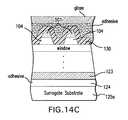
- FIG. 14Cis a cross-sectional view of the solar cell of FIG. 14B after the next process step
- FIG. 15is a cross-sectional view of the solar cell of FIG. 14B after the next process step in a third embodiment of the present invention.
- FIG. 16is a graph of the doping profile in a base layer in the metamorphic solar cell according to the present invention.
- FIG. 17is a cross-sectional view of an interconnection scheme of an array of solar cells according to the prior art.
- FIG. 18is a cross-sectional view of an interconnection scheme of an array of solar cells according to a first embodiment of present invention.
- FIG. 19is a cross-sectional view of an interconnection scheme of an array of solar cells according to a second embodiment of the present invention.
- the basic concept of fabricating an inverted metamorphic multijunction (IMM) solar cellis to grow the subcells of the solar cell on a substrate in a “reverse” sequence. That is, the high band gap subcells (i.e. subcells with band gaps in the range of 1.8 to 2.1 eV), which would normally be the “top” subcells facing the solar radiation, are grown epitaxially on a semiconductor growth substrate, such as for example GaAs or Ge, and such subcells are therefore lattice-matched to such substrate.
- a semiconductor growth substratesuch as for example GaAs or Ge
- One or more lower band gap middle subcellsi.e. with band gaps in the range of 1.2 to 1.8 eV
- At least one lower subcellis formed over the middle subcell such that the at least one lower subcell is substantially lattice mismatched with respect to the growth substrate and such that the at least one lower subcell has a third lower band gap (i.e. a band gap in the range of 0.7 to 1.2 eV).
- a surrogate substrate or support structureis provided over the “bottom” or substantially lattice mismatched lower subcell, and the growth semiconductor substrate is subsequently removed. (The growth substrate may then subsequently be re-used for the growth of a second and subsequent solar cells).
- the present inventionis directed to a method of utilizing the surrogate substrate as a carrier for subsequently forming individual, spaced apart solar cells, and interconnecting such cells in an electrical circuit. More specifically the method includes bonding an inverted photovoltaic cell wafer (i.e. with the top or sunward facing subcell at the top) on a carrier wafer, such as silicon (Si) or germanium (Ge), using an appropriate permanent adhesive, thinning the growth substrate (by grinding/lapping and etching) until the device layers are reached, and then further processing the wafer to make individual solar cells or die, with the top subcell of each solar cell having gridlines, a bus bar, and a top contact.
- a carrier wafersuch as silicon (Si) or germanium (Ge)
- One optional step of the processingwould be to make a backcontact for each solar cell accessible from the front side of the wafer, which enables testing on-wafer.
- the backmetalis etched away in-between the individual solar cells, electrically isolating them, but enabling electrical interconnection of the cells on the wafer by welding, soldering or wire bonding, leaving a minimum of two outside terminals or bond pads to the whole wafer.
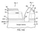
- FIG. 2depicts the multijunction solar cell according to the present invention after the sequential formation of the three subcells A, B and C on a GaAs growth substrate. More particularly, there is shown a substrate 101 , which is preferably gallium arsenide (GaAs), but may also be germanium (Ge) or other suitable material.
- the substrateis preferably a 15° off-cut substrate, that is to say, its surface is orientated 15° off the (100) plane towards the (111)A plane, as more fully described in U.S. patent application Ser. No. 12/047,944, filed Mar. 13, 2008.
- the subcell Aconsisting of an n+ emitter layer 106 and a p-type base layer 107 , is then epitaxially deposited on the window layer 105 .
- the subcell Ais generally lattice matched to the growth substrate 101 .
- the multijunction solar cell structurecould be formed by any suitable combination of group III to V elements listed in the periodic table subject to lattice constant and the band gap requirements, wherein the group III includes boron (B), aluminum (Al), gallium (Ga), indium (In), and thallium (Tl).
- the group IVincludes carbon (C), silicon (Si), germanium (Ge), and tin (Sn).
- the group Vincludes nitrogen (N), phosphorus (P), arsenic (As), antimony (Sb), and bismuth (Bi).
- the emitter layer 106is composed of InGa(Al)P and the base layer 107 is composed of InGa(Al)P.
- the aluminum or Al term in parenthesis in the preceding formulameans that Al is an optional constituent, and in this instance may be used in an amount ranging from 0% to 30%.
- the doping profile of the emitter and base layers 106 and 107 according to the present inventionwill be discussed in conjunction with FIG. 16 .
- Subcell Awill ultimately become the “top” subcell of the inverted metamorphic structure after completion of the process steps according to the present invention to be described hereinafter.
- a back surface field (“BSF”) layer 108is deposited and used to reduce recombination loss, preferably p+ AlGaInP.
- the BSF layer 108drives minority carriers from the region near the base/BSF interface surface to minimize the effect of recombination loss. In other words, the BSF layer 108 reduces recombination loss at the backside of the solar subcell A and thereby reduces the recombination in the base.
- a sequence of heavily doped p-type and n-type layers 109which forms a tunnel diode which is an ohmic circuit element to connect subcell A to subcell B.
- These layersare preferably composed of p++ AlGaAs, and n++ InGaP.
- subcell BOn top of the window layer 110 the layers of subcell B are deposited: the n-type emitter layer 111 and the p-type base layer 112 . These layers are preferably composed of InGaP and In 0.015 GaAs respectively (for a Ge substrate or growth template), or InGaP and GaAs respectively (for a GaAs substrate), although any other suitable materials consistent with lattice constant and band gap requirements may be used as well.
- subcell Bmay be composed of a GaAs, GaInP, GaInAs, GaAsSb, or GaInAsN emitter region and a GaAs, GaInAs, GaAsSb, or GaInAsN base region.
- the doping profile of layers 111 and 112 according to the present inventionwill be discussed in conjunction with FIG. 16 .
- a BSF layer 113which performs the same function as the BSF layer 109 .
- a p++/n++ tunnel diode 114is deposited over the BSF layer 113 similar to the layers 109 , again forming an ohmic circuit element to connect subcell B to subcell C.
- These layers 114are preferably composed of p++ AlGaAs and n++ InGaP.
- a barrier layer 115preferably composed of n-type InGa(Al)P, is deposited over the tunnel diode 114 , to a thickness of about 1.0 micron.
- Such barrier layeris intended to prevent threading dislocations from propagating, either opposite to the direction of growth into the middle and top subcells B and C, or in the direction of growth into the bottom subcell A, and is more particularly described in copending U.S. patent application Ser. No. 11/860,183, filed Sep. 24, 2007.
- a metamorphic layer (or graded interlayer) 116is deposited over the barrier layer 115 using a surfactant.
- Layer 116is preferably a compositionally step-graded series of InGaAlAs layers, preferably with monotonically changing lattice constant, so as to achieve a gradual transition in lattice constant in the semiconductor structure from subcell B to subcell C while minimizing threading dislocations from occurring.
- the band gap of layer 116is constant throughout its thickness, preferably approximately 1.5 eV or otherwise consistent with a value slightly greater than the band gap of the middle subcell B.
- the preferred embodiment of the graded interlayermay also be expressed as being composed of (In x Ga 1-x ) y Al 1-y As, with x and y selected such that the band gap of the interlayer remains constant at approximately 1.50 eV.
- a suitable chemical elementis introduced into the reactor during the growth of layer 116 to improve the surface characteristics of the layer.
- such elementmay be a dopant or donor atom such as selenium (Se) or tellurium (Te). Small amounts of Se or Te are therefore incorporated in the metamorphic layer 116 at the end of the growth process, and remain in the finished solar cell.
- Se or Teare the preferred n-type dopant atoms, other non-isoelectronic surfactants may be used as well.
- isoelectronic surfactantAs an alternative to the use of non-isoelectronic surfactants one may use an isoelectronic surfactant.
- isoelectronicrefers to surfactants such as antimony (Sb) or bismuth (Bi), since such elements have the same number of valence electrons as the P of InGaP, or as in InGaAlAs, in the metamorphic buffer layer.
- Sb or Bi surfactantswill not typically be incorporated into the metamorphic layer 116 .
- the “middle” cell Bis the uppermost or top subcell in the final solar cell, wherein the “top” subcell B would typically have a band gap of 1.8 to 1.9 eV, then the band gap of the interlayer would remain constant at 1.9 eV.
- the metamorphic layerconsists of nine compositionally graded InGaP steps, with each step layer having a thickness of 0.25 micron.
- each layer of Wanlass et al.has a different band gap.
- the layer 116is composed of a plurality of layers of InGaAlAs, with monotonically changing lattice constant, each layer having the same band gap, approximately 1.5 eV.
- one embodiment of the present inventionutilizes a plurality of layers of InGaAlAs for the metamorphic layer 116 for reasons of manufacturability and radiation transparency
- other embodiments of the present inventionmay utilize different material systems to achieve a change in lattice constant from subcell B to subcell C.
- the system of Wanlass using compositionally graded InGaPis a second embodiment of the present invention.
- Other embodiments of the present inventionmay utilize continuously graded, as opposed to step graded, materials.
- the graded interlayermay be composed of any of the As, P, N, Sb based III-V compound semiconductors subject to the constraints of having the in-plane lattice parameter greater or equal to that of the second solar cell and less than or equal to that of the third solar cell, and having a band gap energy greater than that of the second solar cell.
- an optional second barrier layer 117may be deposited over the InGaAlAs metamorphic layer 116 .
- the second barrier layer 117will typically have a different composition than that of barrier layer 115 , and performs essentially the same function of preventing threading dislocations from propagating.
- barrier layer 117is n+ type GaInP.
- a window layer 118 preferably composed of n+ type GaInPis then deposited over the barrier layer 117 (or directly over layer 116 , in the absence of a second barrier layer). This window layer operates to reduce the recombination loss in subcell “C”. It should be apparent to one skilled in the art that additional layers may be added or deleted in the cell structure without departing from the scope of the present invention.
- the layers of cell Care deposited: the n+ emitter layer 119 , and the p-type base layer 120 .
- These layersare preferably composed of n type InGaAs and p type InGaAs respectively, or n type InGaP and p type InGaAs for a heterojunction subcell, although other suitable materials consistent with lattice constant and band gap requirements may be used as well.
- the doping profile of layers 119 and 120will be discussed in connection with FIG. 16 .
- a BSF layer 121preferably composed of InGaAlAs, is then deposited on top of the cell C, the BSF layer performing the same function as the BSF layers 108 and 113 .
- a high band gap contact layer 122preferably composed of InGaAlAs, is deposited on the BSF layer 121 .
- FIG. 3is a cross-sectional view of the solar cell of FIG. 2 after the next process step in which a metal contact layer 123 is deposited over the p+ semiconductor contact layer 122 .
- the metalis preferably the sequence of metal layers Ti/Au/Ag/Au.
- the metal contact scheme chosenis one that has a planar interface with the semiconductor, after heat treatment to activate the ohmic contact. This is done so that (1) a dielectric layer separating the metal from the semiconductor doesn't have to be deposited and selectively etched in the metal contact areas; and (2) the contact layer is specularly reflective over the wavelength range of interest.
- FIG. 4is a cross-sectional view of the solar cell of FIG. 3 after the next process step in which an adhesive layer 124 is deposited over the metal layer 123 .
- the adhesiveis preferably Wafer Bond (manufactured by Brewer Science, Inc. of Rolla, Mo.).
- FIG. 5Ais a cross-sectional view of the solar cell of FIG. 4 after the next process step in which a surrogate substrate 125 , preferably sapphire, is attached.
- the surrogate substratemay be GaAs, Ge or Si, or other suitable material.
- the surrogate substrateis about 40 mils in thickness, and is perforated with holes about 1 mm in diameter, spaced 4 mm apart, to aid in subsequent removal of the adhesive and the substrate.
- a suitable substratee.g., GaAs
- FIG. 6is a simplified cross-sectional view of the solar cell of FIG. 5B depicting just a few of the top layers and lower layers over the surrogate substrate 125 .
- FIG. 7is a cross-sectional view of the solar cell of FIG. 6 after the next process step in which the etch stop layer 103 is removed by a HCl/H 2 O solution.
- FIG. 8is a cross-sectional view of the solar cell of FIG. 7 after the next sequence of process steps in which a photoresist mask (not shown) is placed over the contact layer 104 to form the grid lines 501 .
- the grid lines 501are deposited via evaporation and lithographically patterned and deposited over the contact layer 104 .
- the maskis subsequently lifted off to form the finished metal grid lines 501 as depicted in the Figures.
- the grid lines 501are formed as follows. Prior to the metal deposition, of the n-contact, residual oxide is removed by soaking the wafer in a solution of 15H 2 0:1NH 4 OH for one minute and spin dried in N 2 . The wafer is loaded in the deposition chamber within 30 minutes to preclude excessive oxide growth.
- the metallizationin the preferred embodiment, the sequence of layers of (50 nm Pd/100 nm Ge/30 nm Ti/30 nm Pd/5 ⁇ m Ag/100 nm Au) is e-beam evaporated during one vacuum cycle.
- the background chamber pressure at the beginning of depositionis 5 ⁇ 10 ⁇ 7 torr.
- the grid lines 501 and bus barare defined by liftoff.
- the contact sinteringis performed in lab ambient atmosphere on a hot plate.
- the waferis placed grid side down on a clean silicon wafer on a hot plate set at 120° C.
- the wafer and silicon carrierare allowed to equilibrate for 5 min.
- the hot plateis then set at the sintering temperature (set point 215 ). Ten minutes is allowed for the wafer to attain the sintering temperature.
- the contactthen sinters for 40 min.
- the hot plate temperatureis then dropped in ten minutes to 120° C.
- the Si carrier and waferare removed from the hot plate.
- FIG. 9is a cross-sectional view of the solar cell of FIG. 8 after the next process step in which the grid lines are used as a mask to etch down the surface to the window layer 105 using a citric acid/peroxide etching mixture.
- FIG. 10Ais a top plan view of a wafer in which four solar cells are implemented.
- the depiction of four cellsis for illustration purposes only, and the present invention is not limited to any specific number of cells per wafer.
- each cellthere are grid lines 501 (more particularly shown in cross-section in FIG. 9 ), an interconnecting bus line 502 , and a contact pad 503 electrically connected to the bus line 502 .
- the geometry and number of grid and bus linesis illustrative and the present invention is not limited to the illustrated embodiment.
- a portion of the top surface of each of the cellsis etched down to the metal layer 123 to form a contact pad 504 to the metal layer 123 that is accessible from the front side of the wafer.
- FIG. 10Bis a bottom plan view of the wafer with four solar cells shown in FIG. 10A .
- the metal contact layer 123as shown in the cross-sectional view of FIG. 15 is depicted.
- FIG. 10Cis a top plan view of a wafer in which the solar cells are interconnected according to a first embodiment of the present invention in which wire bonds are used as the electrical interconnects. More specifically, wire bond 708 electrically connects the bottom contact pad 702 of cell 3 with the front contact pad 707 of cell 4 . Similarly wire bond 709 connects bottom contact pad 705 of cell 4 and front contact pad 720 of cell 2 , and wire bond 710 connects bottom contact pad 721 with front contact pad 503 of cell 1 . The cross-sectional view of this wafer through the B-B plane is shown in FIG. 18 .
- FIG. 10Dis a top plan view of a wafer in which the solar cells are interconnected according to a second embodiment of the present invention by a thin film metal interconnects.
- the Figuredepicts the embodiment in which thin film interconnect 722 connects the bottom contact pad 702 of cell 3 with front contact pad 707 of cell 4 .
- thin film interconnect 723connects bottom pad 705 of cell 4 with front contact part 720 of cell 2 .
- Thin film interconnect 724connects bottom pad 724 of cell 2 with front contact pad 503 of cell 1 .
- the cross-sectional view of the wafer through the C-C planeis shown in FIG. 19 .
- FIG. 11is a cross-sectional view of the solar cell of FIG. 9 after the next process step in which an antireflective (ARC) dielectric coating layer 130 is applied over the entire surface of the “bottom” side of the wafer with the grid lines 501 .
- ARCantireflective
- FIG. 12is a cross-sectional view of the solar cell of FIG. 11 after the next process step according to the present invention in which a channel 510 or portion of the semiconductor structure is etched down to the metal layer 123 using phosphide and arsenide etchants defining a peripheral boundary and leaving a mesa structure which constitutes the solar cell.
- the cross-section depicted in FIG. 12is that as seen from the A-A plane shown in FIG. 13 .
- the same etching process which forms the channel 510is used to form the contact pad 504 to metal layer 123 . Reference may be made to FIG. 14A described below.
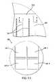
- FIG. 13is a top plan view of the wafer of FIG. 12 depicting the channel 510 etched around the periphery of each cell using phosphide and arsenide etchants.
- FIG. 14Ais an enlarged cross-sectional view of the solar cell of FIG. 10C between cell 3 and cell 4 showing a wire bond 708 electrically interconnecting bottom contact pad 702 and front contact pad 707 of adjacent solar cells mounted on surrogate substrate or support 124 .
- FIG. 14Bis a cross-sectional view of the solar cell of FIG. 12 after the next process step in a first embodiment of the present invention in which the surrogate substrate 125 is appropriately thinned to a relatively thin layer 125 a , by grinding, lapping, or etching.
- FIG. 14Cis a cross-sectional view of the solar cell of FIG. 14B after the next process step in a second embodiment of the present invention in which a cover glass is secured to the top of the cell by an adhesive.
- FIG. 15is a cross-sectional view of the solar cell of FIG. 14C after the next process step in a third embodiment of the present invention in which a cover glass is secured to the top of the cell and the surrogate substrate 125 is entirely removed, leaving only the metal contact layer 123 which forms the backside contact of the solar cell.
- the surrogate substratemay be reused in subsequent wafer processing operations.
- FIG. 16is a graph of a doping profile in the emitter and base layers in one or more subcells of the inverted metamorphic multifunction solar cell of the present invention.
- the various doping profiles within the scope of the present invention, and the advantages of such doping profilesare more particularly described in copending U.S. patent application Ser. No. 11/956,069 filed Dec. 13, 2007, herein incorporated by reference.
- the doping profiles depicted hereinare merely illustrative, and other more complex profiles may be utilized as would be apparent to those skilled in the art without departing from the scope of the present invention.
- FIG. 17is a cross-sectional view of an interconnection scheme of an array of thermophotovoltaic cells known in the prior art.
- the Figuredepicts an InP wafer 600 which forms a semi-insulating substrate on which a number of discrete thermophotovoltaic devices are formed. More particularly, the wafer or substrate 600 is used as a growth substrate on which a lateral conduction layer 601 , and active layers 602 of semiconductor material are grown. After growth of the active layers 602 , a photolithographic process is used to pattern the layers 601 , 602 into spaced apart discrete devices 610 , 620 , 630 , 640 and 650 .
- the lateral conduction layer 601 associated with device 610extends peripherally beyond the edges of the active layer 602 of device 610 to form a contact pad or area to allow a wire bond or other electrical interconnect 651 (such as a thin film interconnect) to be made to the bottom or first terminal of device 610 .
- Such devicesare sometimes referred to as a MIM (Monolithic Interconnected Module).
- a top contact layer 603(such as a metal bond pad) is formed on the top of the active layers of device 610 , to allow a wire bond or other electrical interconnect to be made to the top, or second terminal, of device 610 .
- Similar terminal pad structures and electrical interconnectsare associated with respective devices 620 , 630 , 640 and 650 as depicted in the Figure.
- wire bonds 651 , 652 , 653 , and 654interconnect the devices. More specifically, wire bond 651 extends from layer 601 of device 610 to layer 603 of device 620 . Similar interconnections are made from 620 to 630 , etc. In MIMs, thin film metal interconnects are utilized.
- FIG. 18is a cross-sectional view of an interconnection scheme of an array of photovoltaic cells according to a first embodiment of the present invention, depicting the cross-section through the B-B plane of FIG. 10C .
- the Figuredepicts the carrier wafer 700 with two discrete photovoltaic devices 703 and 706 shown in cross-section. More particularly, the wafer or substrate 700 is adhesively attached by adhesive 701 to back metal contact 123 of the wafer 500 (as shown in FIG. 10B ), and a photolithographic process is used to pattern the wafer into spaced apart discrete devices 703 , 706 , etc.
- a further photolithographic processpatterns and etches down to the back metal contact layer 123 associated with each device so that a contact pad 702 , 705 extends peripherally beyond the edges of the devices 703 , 706 to form a contact pad or area to allow a wire bond or other electrical interconnect to be made to the bottom or first terminal of device 703 , 706 respectively.
- a top contact layer 704 and 707(such as metal bond pad) is formed on the top of the active layers of devices 703 and 706 respectively, to allow a wire bond or other electrical interconnect to be made to the top, or second terminal, of device, 703 and 706 .
- the present inventionis comprised of the following sequence of steps: (1) attaching inverted (i.e., high band gap cells grown first), metalized, photovoltaic cell wafers onto a rigid carrier (semi-insulating Ge or Si, for example, or thermally conductive carriers if needed, such as AlN), metalized face down, with a permanent adhesive; (2) thinning the wafers; (3) processing the devices, (4) separating the individual devices by mesa etching, during which a backcontact is also made; (5) etching through the backmetal to completely separate the devices; (6) interconnecting the individual devices by thin film conductors; and (7) optionally thinning the carrier by grinding, lapping and/or etching (if need be, to reduce weight).
- the front (device) sideshould be protected during the thinning step. Etchants can be prevented from getting to the front side, either with protective coatings, or by meniscus etching, where etchants do not come into contact with the front side.
- the final thickness of the carrier wafermay be chosen for the optimum combination of strength, rigidity, low weight, and thermal conductance.
- the adhesivecan also be chosen to have good thermal conductivity, if required, for example for solar cells used in terrestrial concentrator photovoltaic applications.
- Another adhesive or bondcan be an eutectic bond between gold on the device wafer and the Si or Ge carrier wafer, in which case the backmetal would also serve as part of the bond.
- the backcontact metalcan be accessed as before, by etching down to the metal, from the front side.
- the front side backcontacti.e., the backcontact as accessed from the front side of the wafer
- the front side backcontactcan be also used to interconnect the cells together, by connecting the backcontact of one cell to the front contact of the next, and so on, in different string combinations (series and parallel connections may be defined for different voltage and current specifications for the wafer as a whole).
- the interconnection of individual solar cells according to the present inventioncan be done by welding, soldering or wire bonding, and since such interconnections will be done on one wafer at a time, the set-up costs are much less than if individual discrete cells are to be aligned and die-bonded onto a platform and then interconnected.
- the packing density of cells on the wafer according to the present inventioncan be potentially higher than if individual cells were bonded close together, as on the wafer the separation between cells is defined lithographically, and not by physical/visual alignment as in the individual die case.
- the wafercan be cut into shapes that would allow close packing onto a receiver board, for example for a concentrator system where the whole board gets uniform concentrated light from a mirror or lens.
- bypass diodesfor cell protection, if needed, can also be processed on the wafer in the same way.
- the extra bypass diode layershave to be grown first (below the top cell), and etched off selectively at the start of the device processing, after the device wafer is thinned.
- the bypass diodewill be grounded to the backside contact of each cell in the array.
- the present inventioncan apply to stacks with fewer or greater number of subcells, i.e. two junction cells, four junction cells, five junction cells, etc. In the case of four or more junction cells, the use of more than one metamorphic grading interlayer may also be utilized.
- the subcellsmay alternatively be contacted by means of metal contacts to laterally conductive semiconductor layers between the subcells. Such arrangements may be used to form 3-terminal, 4-terminal, and in general, n-terminal devices.
- the subcellscan be interconnected in circuits using these additional terminals such that most of the available photogenerated current density in each subcell can be used effectively, leading to high efficiency for the multijunction cell, notwithstanding that the photogenerated current densities are typically different in the various subcells.
- the present inventionmay utilize an arrangement of one or more, or all, homojunction cells or subcells, i.e., a cell or subcell in which the p-n junction is formed between a p-type semiconductor and an n-type semiconductor both of which have the same chemical composition and the same band gap, differing only in the dopant species and types, and one or more heterojunction cells or subcells.
- Subcell Awith p-type and n-type InGaP is one example of a homojunction subcell.
- the present inventionmay utilize one or more, or all, heterojunction cells or subcells, i.e., a cell or subcell in which the p-n junction is formed between a p-type semiconductor and an n-type semiconductor having different chemical compositions of the semiconductor material in the n-type regions, and/or different band gap energies in the p-type regions, in addition to utilizing different dopant species and type in the p-type and n-type regions that form the p-n junction.
- heterojunction cells or subcellsi.e., a cell or subcell in which the p-n junction is formed between a p-type semiconductor and an n-type semiconductor having different chemical compositions of the semiconductor material in the n-type regions, and/or different band gap energies in the p-type regions, in addition to utilizing different dopant species and type in the p-type and n-type regions that form the p-n junction.
- the composition of the window or BSF layersmay utilize other semiconductor compounds, subject to lattice constant and band gap requirements, and may include AlInP, AlAs, AlP, AlGaInP, AlGaAsP, AlGaInAs, AlGaInPAs, GaInP, GaInAs, GaInPAs, AlGaAs, AlInAs, AlInPAs, GaAsSb, AlAsSb, GaAlAsSb, AlInSb, GaInSb, AlGaInSb, AlN, GaN, InN, GaInN, AlGaInN, GaInNAs, AlGaInNAs, ZnSSe, CdSSe, and similar materials, and still fall within the spirit of the present invention.
Landscapes
- Photovoltaic Devices (AREA)
Abstract
Description
Claims (44)
Priority Applications (2)
| Application Number | Priority Date | Filing Date | Title |
|---|---|---|---|
| US12/187,477US8263853B2 (en) | 2008-08-07 | 2008-08-07 | Wafer level interconnection of inverted metamorphic multijunction solar cells |
| US13/560,663US8586859B2 (en) | 2008-08-07 | 2012-07-27 | Wafer level interconnection of inverted metamorphic multijunction solar cells |
Applications Claiming Priority (1)
| Application Number | Priority Date | Filing Date | Title |
|---|---|---|---|
| US12/187,477US8263853B2 (en) | 2008-08-07 | 2008-08-07 | Wafer level interconnection of inverted metamorphic multijunction solar cells |
Related Child Applications (1)
| Application Number | Title | Priority Date | Filing Date |
|---|---|---|---|
| US13/560,663DivisionUS8586859B2 (en) | 2008-08-07 | 2012-07-27 | Wafer level interconnection of inverted metamorphic multijunction solar cells |
Publications (2)
| Publication Number | Publication Date |
|---|---|
| US20100031994A1 US20100031994A1 (en) | 2010-02-11 |
| US8263853B2true US8263853B2 (en) | 2012-09-11 |
Family
ID=41651785
Family Applications (2)
| Application Number | Title | Priority Date | Filing Date |
|---|---|---|---|
| US12/187,477Active2031-06-12US8263853B2 (en) | 2008-08-07 | 2008-08-07 | Wafer level interconnection of inverted metamorphic multijunction solar cells |
| US13/560,663ActiveUS8586859B2 (en) | 2008-08-07 | 2012-07-27 | Wafer level interconnection of inverted metamorphic multijunction solar cells |
Family Applications After (1)
| Application Number | Title | Priority Date | Filing Date |
|---|---|---|---|
| US13/560,663ActiveUS8586859B2 (en) | 2008-08-07 | 2012-07-27 | Wafer level interconnection of inverted metamorphic multijunction solar cells |
Country Status (1)
| Country | Link |
|---|---|
| US (2) | US8263853B2 (en) |
Cited By (25)
| Publication number | Priority date | Publication date | Assignee | Title |
|---|---|---|---|---|
| US20110132447A1 (en)* | 2009-12-07 | 2011-06-09 | Epistar Corporation | Solar cell devices and apparatus comprising the same |
| US8586859B2 (en) | 2008-08-07 | 2013-11-19 | Emcore Solar Power, Inc. | Wafer level interconnection of inverted metamorphic multijunction solar cells |
| US8778199B2 (en) | 2009-02-09 | 2014-07-15 | Emoore Solar Power, Inc. | Epitaxial lift off in inverted metamorphic multijunction solar cells |
| US8895342B2 (en) | 2007-09-24 | 2014-11-25 | Emcore Solar Power, Inc. | Heterojunction subcells in inverted metamorphic multijunction solar cells |
| US20150040971A1 (en)* | 2013-08-07 | 2015-02-12 | Emcore Solar Power, Inc. | Fabrication of solar cells with electrically conductive polyimide adhesive |
| US20150053248A1 (en)* | 2013-08-21 | 2015-02-26 | Sunpower Corporation | Interconnection of solar cells in a solar cell module |
| US8969712B2 (en) | 2009-03-10 | 2015-03-03 | Solaero Technologies Corp. | Four junction inverted metamorphic multijunction solar cell with a single metamorphic layer |
| US9018519B1 (en) | 2009-03-10 | 2015-04-28 | Solaero Technologies Corp. | Inverted metamorphic multijunction solar cells having a permanent supporting substrate |
| US20150340528A1 (en)* | 2012-12-10 | 2015-11-26 | Alliance For Sustainable Energy, Llc | Monolithic tandem voltage-matched multijuntion solar cells |
| US9287438B1 (en) | 2008-07-16 | 2016-03-15 | Solaero Technologies Corp. | Method for forming ohmic N-contacts at low temperature in inverted metamorphic multijunction solar cells with contaminant isolation |
| US9758261B1 (en) | 2015-01-15 | 2017-09-12 | Solaero Technologies Corp. | Inverted metamorphic multijunction solar cell with lightweight laminate substrate |
| US9768326B1 (en) | 2013-08-07 | 2017-09-19 | Solaero Technologies Corp. | Fabrication of solar cells with electrically conductive polyimide adhesive |
| US9929300B2 (en) | 2015-11-13 | 2018-03-27 | Solaero Technologies Corp. | Multijunction solar cells with electrically conductive polyimide adhesive |
| US9935209B2 (en) | 2016-01-28 | 2018-04-03 | Solaero Technologies Corp. | Multijunction metamorphic solar cell for space applications |
| US9985161B2 (en) | 2016-08-26 | 2018-05-29 | Solaero Technologies Corp. | Multijunction metamorphic solar cell for space applications |
| US10153388B1 (en) | 2013-03-15 | 2018-12-11 | Solaero Technologies Corp. | Emissivity coating for space solar cell arrays |
| US10170656B2 (en) | 2009-03-10 | 2019-01-01 | Solaero Technologies Corp. | Inverted metamorphic multijunction solar cell with a single metamorphic layer |
| US10256359B2 (en) | 2015-10-19 | 2019-04-09 | Solaero Technologies Corp. | Lattice matched multijunction solar cell assemblies for space applications |
| US10263134B1 (en) | 2016-05-25 | 2019-04-16 | Solaero Technologies Corp. | Multijunction solar cells having an indirect high band gap semiconductor emitter layer in the upper solar subcell |
| US10270000B2 (en) | 2015-10-19 | 2019-04-23 | Solaero Technologies Corp. | Multijunction metamorphic solar cell assembly for space applications |
| US10361330B2 (en) | 2015-10-19 | 2019-07-23 | Solaero Technologies Corp. | Multijunction solar cell assemblies for space applications |
| US10403778B2 (en) | 2015-10-19 | 2019-09-03 | Solaero Technologies Corp. | Multijunction solar cell assembly for space applications |
| US10541349B1 (en) | 2008-12-17 | 2020-01-21 | Solaero Technologies Corp. | Methods of forming inverted multijunction solar cells with distributed Bragg reflector |
| US10636926B1 (en) | 2016-12-12 | 2020-04-28 | Solaero Technologies Corp. | Distributed BRAGG reflector structures in multijunction solar cells |
| US12336305B1 (en) | 2023-10-13 | 2025-06-17 | Tandem PV | Photovoltaic cells with bypass diodes |
Families Citing this family (45)
| Publication number | Priority date | Publication date | Assignee | Title |
|---|---|---|---|---|
| US20090078310A1 (en)* | 2007-09-24 | 2009-03-26 | Emcore Corporation | Heterojunction Subcells In Inverted Metamorphic Multijunction Solar Cells |
| US20100229913A1 (en)* | 2009-01-29 | 2010-09-16 | Emcore Solar Power, Inc. | Contact Layout and String Interconnection of Inverted Metamorphic Multijunction Solar Cells |
| US9117966B2 (en) | 2007-09-24 | 2015-08-25 | Solaero Technologies Corp. | Inverted metamorphic multijunction solar cell with two metamorphic layers and homojunction top cell |
| US9634172B1 (en) | 2007-09-24 | 2017-04-25 | Solaero Technologies Corp. | Inverted metamorphic multijunction solar cell with multiple metamorphic layers |
| US20090078309A1 (en)* | 2007-09-24 | 2009-03-26 | Emcore Corporation | Barrier Layers In Inverted Metamorphic Multijunction Solar Cells |
| US20100122724A1 (en) | 2008-11-14 | 2010-05-20 | Emcore Solar Power, Inc. | Four Junction Inverted Metamorphic Multijunction Solar Cell with Two Metamorphic Layers |
| US10381501B2 (en) | 2006-06-02 | 2019-08-13 | Solaero Technologies Corp. | Inverted metamorphic multijunction solar cell with multiple metamorphic layers |
| US20100203730A1 (en)* | 2009-02-09 | 2010-08-12 | Emcore Solar Power, Inc. | Epitaxial Lift Off in Inverted Metamorphic Multijunction Solar Cells |
| US20100093127A1 (en)* | 2006-12-27 | 2010-04-15 | Emcore Solar Power, Inc. | Inverted Metamorphic Multijunction Solar Cell Mounted on Metallized Flexible Film |
| US20110041898A1 (en)* | 2009-08-19 | 2011-02-24 | Emcore Solar Power, Inc. | Back Metal Layers in Inverted Metamorphic Multijunction Solar Cells |
| US10381505B2 (en) | 2007-09-24 | 2019-08-13 | Solaero Technologies Corp. | Inverted metamorphic multijunction solar cells including metamorphic layers |
| US20090155952A1 (en)* | 2007-12-13 | 2009-06-18 | Emcore Corporation | Exponentially Doped Layers In Inverted Metamorphic Multijunction Solar Cells |
| US20100012175A1 (en) | 2008-07-16 | 2010-01-21 | Emcore Solar Power, Inc. | Ohmic n-contact formed at low temperature in inverted metamorphic multijunction solar cells |
| US20090272430A1 (en)* | 2008-04-30 | 2009-11-05 | Emcore Solar Power, Inc. | Refractive Index Matching in Inverted Metamorphic Multijunction Solar Cells |
| US20090272438A1 (en)* | 2008-05-05 | 2009-11-05 | Emcore Corporation | Strain Balanced Multiple Quantum Well Subcell In Inverted Metamorphic Multijunction Solar Cell |
| US20100012174A1 (en)* | 2008-07-16 | 2010-01-21 | Emcore Corporation | High band gap contact layer in inverted metamorphic multijunction solar cells |
| US8236600B2 (en)* | 2008-11-10 | 2012-08-07 | Emcore Solar Power, Inc. | Joining method for preparing an inverted metamorphic multijunction solar cell |
| US20100122764A1 (en)* | 2008-11-14 | 2010-05-20 | Emcore Solar Power, Inc. | Surrogate Substrates for Inverted Metamorphic Multijunction Solar Cells |
| US9018521B1 (en) | 2008-12-17 | 2015-04-28 | Solaero Technologies Corp. | Inverted metamorphic multijunction solar cell with DBR layer adjacent to the top subcell |
| US7960201B2 (en)* | 2009-01-29 | 2011-06-14 | Emcore Solar Power, Inc. | String interconnection and fabrication of inverted metamorphic multijunction solar cells |
| US20100206365A1 (en)* | 2009-02-19 | 2010-08-19 | Emcore Solar Power, Inc. | Inverted Metamorphic Multijunction Solar Cells on Low Density Carriers |
| US20100229933A1 (en)* | 2009-03-10 | 2010-09-16 | Emcore Solar Power, Inc. | Inverted Metamorphic Multijunction Solar Cells with a Supporting Coating |
| US8283558B2 (en)* | 2009-03-27 | 2012-10-09 | The Boeing Company | Solar cell assembly with combined handle substrate and bypass diode and method |
| US20100282288A1 (en)* | 2009-05-06 | 2010-11-11 | Emcore Solar Power, Inc. | Solar Cell Interconnection on a Flexible Substrate |
| US8263856B2 (en)* | 2009-08-07 | 2012-09-11 | Emcore Solar Power, Inc. | Inverted metamorphic multijunction solar cells with back contacts |
| US8187907B1 (en) | 2010-05-07 | 2012-05-29 | Emcore Solar Power, Inc. | Solder structures for fabrication of inverted metamorphic multijunction solar cells |
| WO2012034993A1 (en)* | 2010-09-13 | 2012-03-22 | Imec | Method for fabricating thin photovoltaic cells |
| US9818901B2 (en)* | 2011-05-13 | 2017-11-14 | International Business Machines Corporation | Wafer bonded solar cells and fabrication methods |
| DE102011115659A1 (en)* | 2011-09-28 | 2013-03-28 | Osram Opto Semiconductors Gmbh | Photovoltaic semiconductor chip |
| US20130240009A1 (en)* | 2012-03-18 | 2013-09-19 | The Boeing Company | Metal Dendrite-free Solar Cell |
| TW201344924A (en)* | 2012-04-23 | 2013-11-01 | Advanced Wireless Semiconductor Company | Negative electrode structure of concentrator photovoltaic |
| US8765578B2 (en)* | 2012-06-06 | 2014-07-01 | International Business Machines Corporation | Edge protection of bonded wafers during wafer thinning |
| US9102422B2 (en) | 2012-06-28 | 2015-08-11 | Solaero Technologies Corp. | Solar cell assembly, solar cell panel, and method for manufacturing the same |
| US9287431B2 (en) | 2012-12-10 | 2016-03-15 | Alliance For Sustainable Energy, Llc | Superstrate sub-cell voltage-matched multijunction solar cells |
| JP6300442B2 (en)* | 2013-01-18 | 2018-03-28 | オリンパス株式会社 | Optical transmission module and imaging device |
| US20160013344A1 (en)* | 2014-07-09 | 2016-01-14 | Emcore Solar Power, Inc. | Method to assemble a rectangular cic from a circular wafer |
| US11316053B2 (en)* | 2016-08-26 | 2022-04-26 | Sol Aero Technologies Corp. | Multijunction solar cell assembly |
| US12249667B2 (en) | 2017-08-18 | 2025-03-11 | Solaero Technologies Corp. | Space vehicles including multijunction metamorphic solar cells |
| US11502213B2 (en)* | 2016-12-30 | 2022-11-15 | Sunpower Corporation | Solar cell having a plurality of sub-cells coupled by cell level interconnection |
| US11955574B2 (en)* | 2017-10-05 | 2024-04-09 | International Business Machines Corporation | Photovoltaic cell form ultra-small IOT device with multi-level voltage output |
| US20190181289A1 (en) | 2017-12-11 | 2019-06-13 | Solaero Technologies Corp. | Multijunction solar cells |
| CN112740425A (en)* | 2018-07-13 | 2021-04-30 | 阵列光子学公司 | Dual-depth via device and process for large back-contact solar cells |
| CN109545898B (en)* | 2018-11-26 | 2025-03-07 | 南昌凯迅光电股份有限公司 | A method for manufacturing radiation-resistant enhanced space GaInP/GaInAs/Ge battery epitaxial wafer |
| US12424965B2 (en) | 2022-06-02 | 2025-09-23 | Antora Energy, Inc. | Layered window in thermophotovoltaic devices |
| WO2024258865A1 (en)* | 2023-06-12 | 2024-12-19 | Antora Energy, Inc. | Monolithic interconnected modules (mims) thin-film photovoltaic (pv) cells |
Citations (89)
| Publication number | Priority date | Publication date | Assignee | Title |
|---|---|---|---|---|
| US3488834A (en) | 1965-10-20 | 1970-01-13 | Texas Instruments Inc | Microelectronic circuit formed in an insulating substrate and method of making same |
| US3964155A (en) | 1972-02-23 | 1976-06-22 | The United States Of America As Represented By The Secretary Of The Navy | Method of planar mounting of silicon solar cells |
| US4001864A (en) | 1976-01-30 | 1977-01-04 | Gibbons James F | Semiconductor p-n junction solar cell and method of manufacture |
| US4255211A (en) | 1979-12-31 | 1981-03-10 | Chevron Research Company | Multilayer photovoltaic solar cell with semiconductor layer at shorting junction interface |
| US4338480A (en) | 1980-12-29 | 1982-07-06 | Varian Associates, Inc. | Stacked multijunction photovoltaic converters |
| US4393576A (en) | 1980-09-26 | 1983-07-19 | Licenta Patent-Verwaltungs-Gmbh | Method of producing electrical contacts on a silicon solar cell |
| US4612408A (en) | 1984-10-22 | 1986-09-16 | Sera Solar Corporation | Electrically isolated semiconductor integrated photodiode circuits and method |
| US4881979A (en) | 1984-08-29 | 1989-11-21 | Varian Associates, Inc. | Junctions for monolithic cascade solar cells and methods |
| US5019177A (en) | 1989-11-03 | 1991-05-28 | The United States Of America As Represented By The United States Department Of Energy | Monolithic tandem solar cell |
| US5021360A (en) | 1989-09-25 | 1991-06-04 | Gte Laboratories Incorporated | Method of farbicating highly lattice mismatched quantum well structures |
| US5053083A (en) | 1989-05-08 | 1991-10-01 | The Board Of Trustees Of The Leland Stanford Junior University | Bilevel contact solar cells |
| US5217539A (en) | 1991-09-05 | 1993-06-08 | The Boeing Company | III-V solar cells and doping processes |
| US5322572A (en) | 1989-11-03 | 1994-06-21 | The United States Of America As Represented By The United States Department Of Energy | Monolithic tandem solar cell |
| US5342453A (en) | 1992-11-13 | 1994-08-30 | Midwest Research Institute | Heterojunction solar cell |
| US5376185A (en) | 1993-05-12 | 1994-12-27 | Midwest Research Institute | Single-junction solar cells with the optimum band gap for terrestrial concentrator applications |
| EP0658944A2 (en) | 1993-12-14 | 1995-06-21 | Spectrolab, Inc. | Thin semiconductor device and method of fabrication |
| US5479032A (en) | 1994-07-21 | 1995-12-26 | Trustees Of Princeton University | Multiwavelength infrared focal plane array detector |
| US5510272A (en) | 1993-12-24 | 1996-04-23 | Mitsubishi Denki Kabushiki Kaisha | Method for fabricating solar cell |
| US5944913A (en) | 1997-11-26 | 1999-08-31 | Sandia Corporation | High-efficiency solar cell and method for fabrication |
| US6165873A (en) | 1998-11-27 | 2000-12-26 | Nec Corporation | Process for manufacturing a semiconductor integrated circuit device |
| US6180432B1 (en) | 1998-03-03 | 2001-01-30 | Interface Studies, Inc. | Fabrication of single absorber layer radiated energy conversion device |
| US6218606B1 (en)* | 1998-09-24 | 2001-04-17 | Sanyo Electric Co., Ltd. | Solar cell module for preventing reverse voltage to solar cells |
| US6239354B1 (en) | 1998-10-09 | 2001-05-29 | Midwest Research Institute | Electrical isolation of component cells in monolithically interconnected modules |
| EP1109230A2 (en) | 1999-12-02 | 2001-06-20 | The Boeing Company | Multijunction photovoltaic cell using a silicon or silicon-germanium substrate |
| US6252287B1 (en) | 1999-05-19 | 2001-06-26 | Sandia Corporation | InGaAsN/GaAs heterojunction for multi-junction solar cells |
| US6281426B1 (en) | 1997-10-01 | 2001-08-28 | Midwest Research Institute | Multi-junction, monolithic solar cell using low-band-gap materials lattice matched to GaAs or Ge |
| US6300557B1 (en) | 1998-10-09 | 2001-10-09 | Midwest Research Institute | Low-bandgap double-heterostructure InAsP/GaInAs photovoltaic converters |
| US6300558B1 (en) | 1999-04-27 | 2001-10-09 | Japan Energy Corporation | Lattice matched solar cell and method for manufacturing the same |
| US6388187B1 (en)* | 1997-12-26 | 2002-05-14 | Canon Kabushiki Kaisha | Photovoltaic element module and its production method, and non-contact treatment method |
| US20020117675A1 (en) | 2001-02-09 | 2002-08-29 | Angelo Mascarenhas | Isoelectronic co-doping |
| US6482672B1 (en) | 1997-11-06 | 2002-11-19 | Essential Research, Inc. | Using a critical composition grading technique to deposit InGaAs epitaxial layers on InP substrates |
| US6660928B1 (en) | 2002-04-02 | 2003-12-09 | Essential Research, Inc. | Multi-junction photovoltaic cell |
| US20030226952A1 (en) | 2002-06-07 | 2003-12-11 | Clark William R. | Three-terminal avalanche photodiode |
| US6690041B2 (en) | 2002-05-14 | 2004-02-10 | Global Solar Energy, Inc. | Monolithically integrated diodes in thin-film photovoltaic devices |
| US20040079408A1 (en) | 2002-10-23 | 2004-04-29 | The Boeing Company | Isoelectronic surfactant suppression of threading dislocations in metamorphic epitaxial layers |
| US20040200523A1 (en) | 2003-04-14 | 2004-10-14 | The Boeing Company | Multijunction photovoltaic cell grown on high-miscut-angle substrate |
| WO2005015638A1 (en) | 2003-07-22 | 2005-02-17 | Akzo Nobel N.V. | Process for manufacturing a solar cell foil using a temporary substrate |
| US20050211291A1 (en) | 2004-03-23 | 2005-09-29 | The Boeing Company | Solar cell assembly |
| US6951819B2 (en) | 2002-12-05 | 2005-10-04 | Blue Photonics, Inc. | High efficiency, monolithic multijunction solar cells containing lattice-mismatched materials and methods of forming same |
| US20050274411A1 (en) | 2004-06-15 | 2005-12-15 | King Richard R | Solar cells having a transparent composition-graded buffer layer |
| US20060021565A1 (en) | 2004-07-30 | 2006-02-02 | Aonex Technologies, Inc. | GaInP / GaAs / Si triple junction solar cell enabled by wafer bonding and layer transfer |
| FR2878076A1 (en) | 2004-11-17 | 2006-05-19 | St Microelectronics Sa | SLIMMING A SEMICONDUCTOR WAFER |
| US20060112986A1 (en) | 2004-10-21 | 2006-06-01 | Aonex Technologies, Inc. | Multi-junction solar cells and methods of making same using layer transfer and bonding techniques |
| US7071407B2 (en) | 2002-10-31 | 2006-07-04 | Emcore Corporation | Method and apparatus of multiplejunction solar cell structure with high band gap heterojunction middle cell |
| US20060144435A1 (en) | 2002-05-21 | 2006-07-06 | Wanlass Mark W | High-efficiency, monolithic, multi-bandgap, tandem photovoltaic energy converters |
| US20060162768A1 (en) | 2002-05-21 | 2006-07-27 | Wanlass Mark W | Low bandgap, monolithic, multi-bandgap, optoelectronic devices |
| US20060185582A1 (en) | 2005-02-18 | 2006-08-24 | Atwater Harry A Jr | High efficiency solar cells utilizing wafer bonding and layer transfer to integrate non-lattice matched materials |
| US7166520B1 (en) | 2005-08-08 | 2007-01-23 | Silicon Genesis Corporation | Thin handle substrate method and structure for fabricating devices using one or more films provided by a layer transfer process |
| US20070137694A1 (en) | 2005-12-16 | 2007-06-21 | The Boeing Company | Notch filter for triple junction solar cells |
| EP1863099A2 (en) | 2006-06-02 | 2007-12-05 | Emcore Corporation | Metamorphic layers in multijunction solar cells |
| US20080029151A1 (en) | 2006-08-07 | 2008-02-07 | Mcglynn Daniel | Terrestrial solar power system using III-V semiconductor solar cells |
| US20080149173A1 (en)* | 2006-12-21 | 2008-06-26 | Sharps Paul R | Inverted metamorphic solar cell with bypass diode |
| US20080185038A1 (en) | 2007-02-02 | 2008-08-07 | Emcore Corporation | Inverted metamorphic solar cell with via for backside contacts |
| US20080190886A1 (en)* | 2007-02-08 | 2008-08-14 | Soo Young Choi | Differential etch rate control of layers deposited by chemical vapor deposition |
| US20080245409A1 (en) | 2006-12-27 | 2008-10-09 | Emcore Corporation | Inverted Metamorphic Solar Cell Mounted on Flexible Film |
| US20090038679A1 (en) | 2007-08-09 | 2009-02-12 | Emcore Corporation | Thin Multijunction Solar Cells With Plated Metal OHMIC Contact and Support |
| US20090078310A1 (en) | 2007-09-24 | 2009-03-26 | Emcore Corporation | Heterojunction Subcells In Inverted Metamorphic Multijunction Solar Cells |
| US20090078309A1 (en) | 2007-09-24 | 2009-03-26 | Emcore Corporation | Barrier Layers In Inverted Metamorphic Multijunction Solar Cells |
| US20090078311A1 (en)* | 2007-09-24 | 2009-03-26 | Emcore Corporation | Surfactant Assisted Growth in Barrier Layers In Inverted Metamorphic Multijunction Solar Cells |
| US20090078308A1 (en)* | 2007-09-24 | 2009-03-26 | Emcore Corporation | Thin Inverted Metamorphic Multijunction Solar Cells with Rigid Support |
| US20090155952A1 (en) | 2007-12-13 | 2009-06-18 | Emcore Corporation | Exponentially Doped Layers In Inverted Metamorphic Multijunction Solar Cells |
| US20090223554A1 (en) | 2008-03-05 | 2009-09-10 | Emcore Corporation | Dual Sided Photovoltaic Package |
| US20090229658A1 (en) | 2008-03-13 | 2009-09-17 | Emcore Corporation | Non-Isoelectronic Surfactant Assisted Growth In Inverted Metamorphic Multijunction Solar Cells |
| US20090229662A1 (en) | 2008-03-13 | 2009-09-17 | Emcore Corporation | Off-Cut Substrates In Inverted Metamorphic Multijunction Solar Cells |
| US20090272430A1 (en) | 2008-04-30 | 2009-11-05 | Emcore Solar Power, Inc. | Refractive Index Matching in Inverted Metamorphic Multijunction Solar Cells |
| US20090272438A1 (en) | 2008-05-05 | 2009-11-05 | Emcore Corporation | Strain Balanced Multiple Quantum Well Subcell In Inverted Metamorphic Multijunction Solar Cell |
| US20090288703A1 (en) | 2008-05-20 | 2009-11-26 | Emcore Corporation | Wide Band Gap Window Layers In Inverted Metamorphic Multijunction Solar Cells |
| US20100012174A1 (en) | 2008-07-16 | 2010-01-21 | Emcore Corporation | High band gap contact layer in inverted metamorphic multijunction solar cells |
| US20100012175A1 (en) | 2008-07-16 | 2010-01-21 | Emcore Solar Power, Inc. | Ohmic n-contact formed at low temperature in inverted metamorphic multijunction solar cells |
| US20100047959A1 (en) | 2006-08-07 | 2010-02-25 | Emcore Solar Power, Inc. | Epitaxial Lift Off on Film Mounted Inverted Metamorphic Multijunction Solar Cells |
| US20100093127A1 (en) | 2006-12-27 | 2010-04-15 | Emcore Solar Power, Inc. | Inverted Metamorphic Multijunction Solar Cell Mounted on Metallized Flexible Film |
| US20100116327A1 (en) | 2008-11-10 | 2010-05-13 | Emcore Corporation | Four junction inverted metamorphic multijunction solar cell |
| US20100122764A1 (en) | 2008-11-14 | 2010-05-20 | Emcore Solar Power, Inc. | Surrogate Substrates for Inverted Metamorphic Multijunction Solar Cells |
| US20100122724A1 (en) | 2008-11-14 | 2010-05-20 | Emcore Solar Power, Inc. | Four Junction Inverted Metamorphic Multijunction Solar Cell with Two Metamorphic Layers |
| US20100147366A1 (en) | 2008-12-17 | 2010-06-17 | Emcore Solar Power, Inc. | Inverted Metamorphic Multijunction Solar Cells with Distributed Bragg Reflector |
| US7741146B2 (en)* | 2008-08-12 | 2010-06-22 | Emcore Solar Power, Inc. | Demounting of inverted metamorphic multijunction solar cells |
| US20100186804A1 (en) | 2009-01-29 | 2010-07-29 | Emcore Solar Power, Inc. | String Interconnection of Inverted Metamorphic Multijunction Solar Cells on Flexible Perforated Carriers |
| US20100203730A1 (en) | 2009-02-09 | 2010-08-12 | Emcore Solar Power, Inc. | Epitaxial Lift Off in Inverted Metamorphic Multijunction Solar Cells |
| US20100206365A1 (en) | 2009-02-19 | 2010-08-19 | Emcore Solar Power, Inc. | Inverted Metamorphic Multijunction Solar Cells on Low Density Carriers |
| US7785989B2 (en) | 2008-12-17 | 2010-08-31 | Emcore Solar Power, Inc. | Growth substrates for inverted metamorphic multijunction solar cells |
| US20100229913A1 (en) | 2009-01-29 | 2010-09-16 | Emcore Solar Power, Inc. | Contact Layout and String Interconnection of Inverted Metamorphic Multijunction Solar Cells |
| US20100229926A1 (en) | 2009-03-10 | 2010-09-16 | Emcore Solar Power, Inc. | Four Junction Inverted Metamorphic Multijunction Solar Cell with a Single Metamorphic Layer |
| US20100229933A1 (en) | 2009-03-10 | 2010-09-16 | Emcore Solar Power, Inc. | Inverted Metamorphic Multijunction Solar Cells with a Supporting Coating |
| US20100233839A1 (en) | 2009-01-29 | 2010-09-16 | Emcore Solar Power, Inc. | String Interconnection and Fabrication of Inverted Metamorphic Multijunction Solar Cells |
| US20100233838A1 (en) | 2009-03-10 | 2010-09-16 | Emcore Solar Power, Inc. | Mounting of Solar Cells on a Flexible Substrate |
| US20100282288A1 (en) | 2009-05-06 | 2010-11-11 | Emcore Solar Power, Inc. | Solar Cell Interconnection on a Flexible Substrate |
| US7842881B2 (en) | 2006-10-19 | 2010-11-30 | Emcore Solar Power, Inc. | Solar cell structure with localized doping in cap layer |
| US20110030774A1 (en) | 2009-08-07 | 2011-02-10 | Emcore Solar Power, Inc. | Inverted Metamorphic Multijunction Solar Cells with Back Contacts |
| US20110041898A1 (en) | 2009-08-19 | 2011-02-24 | Emcore Solar Power, Inc. | Back Metal Layers in Inverted Metamorphic Multijunction Solar Cells |
Family Cites Families (2)
| Publication number | Priority date | Publication date | Assignee | Title |
|---|---|---|---|---|
| US8263853B2 (en) | 2008-08-07 | 2012-09-11 | Emcore Solar Power, Inc. | Wafer level interconnection of inverted metamorphic multijunction solar cells |
| US8187907B1 (en) | 2010-05-07 | 2012-05-29 | Emcore Solar Power, Inc. | Solder structures for fabrication of inverted metamorphic multijunction solar cells |
- 2008
- 2008-08-07USUS12/187,477patent/US8263853B2/enactiveActive
- 2012
- 2012-07-27USUS13/560,663patent/US8586859B2/enactiveActive
Patent Citations (99)
| Publication number | Priority date | Publication date | Assignee | Title |
|---|---|---|---|---|
| US3488834A (en) | 1965-10-20 | 1970-01-13 | Texas Instruments Inc | Microelectronic circuit formed in an insulating substrate and method of making same |
| US3964155A (en) | 1972-02-23 | 1976-06-22 | The United States Of America As Represented By The Secretary Of The Navy | Method of planar mounting of silicon solar cells |
| US4001864A (en) | 1976-01-30 | 1977-01-04 | Gibbons James F | Semiconductor p-n junction solar cell and method of manufacture |
| US4255211A (en) | 1979-12-31 | 1981-03-10 | Chevron Research Company | Multilayer photovoltaic solar cell with semiconductor layer at shorting junction interface |
| US4393576A (en) | 1980-09-26 | 1983-07-19 | Licenta Patent-Verwaltungs-Gmbh | Method of producing electrical contacts on a silicon solar cell |
| US4338480A (en) | 1980-12-29 | 1982-07-06 | Varian Associates, Inc. | Stacked multijunction photovoltaic converters |
| US4881979A (en) | 1984-08-29 | 1989-11-21 | Varian Associates, Inc. | Junctions for monolithic cascade solar cells and methods |
| US4612408A (en) | 1984-10-22 | 1986-09-16 | Sera Solar Corporation | Electrically isolated semiconductor integrated photodiode circuits and method |
| US5053083A (en) | 1989-05-08 | 1991-10-01 | The Board Of Trustees Of The Leland Stanford Junior University | Bilevel contact solar cells |
| US5021360A (en) | 1989-09-25 | 1991-06-04 | Gte Laboratories Incorporated | Method of farbicating highly lattice mismatched quantum well structures |
| US5019177A (en) | 1989-11-03 | 1991-05-28 | The United States Of America As Represented By The United States Department Of Energy | Monolithic tandem solar cell |
| US5322572A (en) | 1989-11-03 | 1994-06-21 | The United States Of America As Represented By The United States Department Of Energy | Monolithic tandem solar cell |
| US5217539A (en) | 1991-09-05 | 1993-06-08 | The Boeing Company | III-V solar cells and doping processes |
| US5342453A (en) | 1992-11-13 | 1994-08-30 | Midwest Research Institute | Heterojunction solar cell |
| US5376185A (en) | 1993-05-12 | 1994-12-27 | Midwest Research Institute | Single-junction solar cells with the optimum band gap for terrestrial concentrator applications |
| EP0658944A2 (en) | 1993-12-14 | 1995-06-21 | Spectrolab, Inc. | Thin semiconductor device and method of fabrication |
| US5510272A (en) | 1993-12-24 | 1996-04-23 | Mitsubishi Denki Kabushiki Kaisha | Method for fabricating solar cell |
| US5479032A (en) | 1994-07-21 | 1995-12-26 | Trustees Of Princeton University | Multiwavelength infrared focal plane array detector |
| US6281426B1 (en) | 1997-10-01 | 2001-08-28 | Midwest Research Institute | Multi-junction, monolithic solar cell using low-band-gap materials lattice matched to GaAs or Ge |
| US6482672B1 (en) | 1997-11-06 | 2002-11-19 | Essential Research, Inc. | Using a critical composition grading technique to deposit InGaAs epitaxial layers on InP substrates |
| US5944913A (en) | 1997-11-26 | 1999-08-31 | Sandia Corporation | High-efficiency solar cell and method for fabrication |
| US6388187B1 (en)* | 1997-12-26 | 2002-05-14 | Canon Kabushiki Kaisha | Photovoltaic element module and its production method, and non-contact treatment method |
| US6180432B1 (en) | 1998-03-03 | 2001-01-30 | Interface Studies, Inc. | Fabrication of single absorber layer radiated energy conversion device |
| US6218606B1 (en)* | 1998-09-24 | 2001-04-17 | Sanyo Electric Co., Ltd. | Solar cell module for preventing reverse voltage to solar cells |
| US6239354B1 (en) | 1998-10-09 | 2001-05-29 | Midwest Research Institute | Electrical isolation of component cells in monolithically interconnected modules |
| US6300557B1 (en) | 1998-10-09 | 2001-10-09 | Midwest Research Institute | Low-bandgap double-heterostructure InAsP/GaInAs photovoltaic converters |
| US6165873A (en) | 1998-11-27 | 2000-12-26 | Nec Corporation | Process for manufacturing a semiconductor integrated circuit device |
| US6300558B1 (en) | 1999-04-27 | 2001-10-09 | Japan Energy Corporation | Lattice matched solar cell and method for manufacturing the same |
| US6252287B1 (en) | 1999-05-19 | 2001-06-26 | Sandia Corporation | InGaAsN/GaAs heterojunction for multi-junction solar cells |
| US6340788B1 (en) | 1999-12-02 | 2002-01-22 | Hughes Electronics Corporation | Multijunction photovoltaic cells and panels using a silicon or silicon-germanium active substrate cell for space and terrestrial applications |
| EP1109230A2 (en) | 1999-12-02 | 2001-06-20 | The Boeing Company | Multijunction photovoltaic cell using a silicon or silicon-germanium substrate |
| US20020117675A1 (en) | 2001-02-09 | 2002-08-29 | Angelo Mascarenhas | Isoelectronic co-doping |
| US6660928B1 (en) | 2002-04-02 | 2003-12-09 | Essential Research, Inc. | Multi-junction photovoltaic cell |
| US6690041B2 (en) | 2002-05-14 | 2004-02-10 | Global Solar Energy, Inc. | Monolithically integrated diodes in thin-film photovoltaic devices |
| US20060162768A1 (en) | 2002-05-21 | 2006-07-27 | Wanlass Mark W | Low bandgap, monolithic, multi-bandgap, optoelectronic devices |
| US20060144435A1 (en) | 2002-05-21 | 2006-07-06 | Wanlass Mark W | High-efficiency, monolithic, multi-bandgap, tandem photovoltaic energy converters |
| US20030226952A1 (en) | 2002-06-07 | 2003-12-11 | Clark William R. | Three-terminal avalanche photodiode |
| US20040079408A1 (en) | 2002-10-23 | 2004-04-29 | The Boeing Company | Isoelectronic surfactant suppression of threading dislocations in metamorphic epitaxial layers |
| US7071407B2 (en) | 2002-10-31 | 2006-07-04 | Emcore Corporation | Method and apparatus of multiplejunction solar cell structure with high band gap heterojunction middle cell |
| US6951819B2 (en) | 2002-12-05 | 2005-10-04 | Blue Photonics, Inc. | High efficiency, monolithic multijunction solar cells containing lattice-mismatched materials and methods of forming same |
| US20040200523A1 (en) | 2003-04-14 | 2004-10-14 | The Boeing Company | Multijunction photovoltaic cell grown on high-miscut-angle substrate |
| WO2005015638A1 (en) | 2003-07-22 | 2005-02-17 | Akzo Nobel N.V. | Process for manufacturing a solar cell foil using a temporary substrate |
| US20050211291A1 (en) | 2004-03-23 | 2005-09-29 | The Boeing Company | Solar cell assembly |
| US20050274411A1 (en) | 2004-06-15 | 2005-12-15 | King Richard R | Solar cells having a transparent composition-graded buffer layer |
| US20060021565A1 (en) | 2004-07-30 | 2006-02-02 | Aonex Technologies, Inc. | GaInP / GaAs / Si triple junction solar cell enabled by wafer bonding and layer transfer |
| US20060112986A1 (en) | 2004-10-21 | 2006-06-01 | Aonex Technologies, Inc. | Multi-junction solar cells and methods of making same using layer transfer and bonding techniques |
| FR2878076A1 (en) | 2004-11-17 | 2006-05-19 | St Microelectronics Sa | SLIMMING A SEMICONDUCTOR WAFER |
| US20070218649A1 (en) | 2004-11-17 | 2007-09-20 | Stmicroelectronics Sa | Semiconductor wafer thinning |
| US20060185582A1 (en) | 2005-02-18 | 2006-08-24 | Atwater Harry A Jr | High efficiency solar cells utilizing wafer bonding and layer transfer to integrate non-lattice matched materials |
| US7166520B1 (en) | 2005-08-08 | 2007-01-23 | Silicon Genesis Corporation | Thin handle substrate method and structure for fabricating devices using one or more films provided by a layer transfer process |
| US20070137694A1 (en) | 2005-12-16 | 2007-06-21 | The Boeing Company | Notch filter for triple junction solar cells |
| EP1863099A2 (en) | 2006-06-02 | 2007-12-05 | Emcore Corporation | Metamorphic layers in multijunction solar cells |
| US20070277873A1 (en) | 2006-06-02 | 2007-12-06 | Emcore Corporation | Metamorphic layers in multijunction solar cells |
| US20100229932A1 (en) | 2006-06-02 | 2010-09-16 | Emcore Solar Power, Inc. | Inverted Metamorphic Multijunction Solar Cells |
| US20080029151A1 (en) | 2006-08-07 | 2008-02-07 | Mcglynn Daniel | Terrestrial solar power system using III-V semiconductor solar cells |
| US20090314348A1 (en) | 2006-08-07 | 2009-12-24 | Mcglynn Daniel | Terrestrial solar power system using iii-v semiconductor solar cells |
| US20100047959A1 (en) | 2006-08-07 | 2010-02-25 | Emcore Solar Power, Inc. | Epitaxial Lift Off on Film Mounted Inverted Metamorphic Multijunction Solar Cells |
| US20090188546A1 (en) | 2006-08-07 | 2009-07-30 | Mcglynn Daniel | Terrestrial solar power system using iii-v semiconductor solar cells |
| US7842881B2 (en) | 2006-10-19 | 2010-11-30 | Emcore Solar Power, Inc. | Solar cell structure with localized doping in cap layer |
| US20080149173A1 (en)* | 2006-12-21 | 2008-06-26 | Sharps Paul R | Inverted metamorphic solar cell with bypass diode |
| US20100236615A1 (en) | 2006-12-21 | 2010-09-23 | Emcore Solar Power, Inc. | Integrated Semiconductor Structure with a Solar Cell and a Bypass Diode |
| US20080245409A1 (en) | 2006-12-27 | 2008-10-09 | Emcore Corporation | Inverted Metamorphic Solar Cell Mounted on Flexible Film |
| US20100093127A1 (en) | 2006-12-27 | 2010-04-15 | Emcore Solar Power, Inc. | Inverted Metamorphic Multijunction Solar Cell Mounted on Metallized Flexible Film |
| US20080185038A1 (en) | 2007-02-02 | 2008-08-07 | Emcore Corporation | Inverted metamorphic solar cell with via for backside contacts |
| US20080190886A1 (en)* | 2007-02-08 | 2008-08-14 | Soo Young Choi | Differential etch rate control of layers deposited by chemical vapor deposition |
| US20090038679A1 (en) | 2007-08-09 | 2009-02-12 | Emcore Corporation | Thin Multijunction Solar Cells With Plated Metal OHMIC Contact and Support |
| US20090078308A1 (en)* | 2007-09-24 | 2009-03-26 | Emcore Corporation | Thin Inverted Metamorphic Multijunction Solar Cells with Rigid Support |
| US20090078311A1 (en)* | 2007-09-24 | 2009-03-26 | Emcore Corporation | Surfactant Assisted Growth in Barrier Layers In Inverted Metamorphic Multijunction Solar Cells |
| US20090078309A1 (en) | 2007-09-24 | 2009-03-26 | Emcore Corporation | Barrier Layers In Inverted Metamorphic Multijunction Solar Cells |
| US20090078310A1 (en) | 2007-09-24 | 2009-03-26 | Emcore Corporation | Heterojunction Subcells In Inverted Metamorphic Multijunction Solar Cells |
| US7727795B2 (en) | 2007-12-13 | 2010-06-01 | Encore Solar Power, Inc. | Exponentially doped layers in inverted metamorphic multijunction solar cells |
| US20090155952A1 (en) | 2007-12-13 | 2009-06-18 | Emcore Corporation | Exponentially Doped Layers In Inverted Metamorphic Multijunction Solar Cells |
| US20090223554A1 (en) | 2008-03-05 | 2009-09-10 | Emcore Corporation | Dual Sided Photovoltaic Package |
| US20090229658A1 (en) | 2008-03-13 | 2009-09-17 | Emcore Corporation | Non-Isoelectronic Surfactant Assisted Growth In Inverted Metamorphic Multijunction Solar Cells |
| US20090229662A1 (en) | 2008-03-13 | 2009-09-17 | Emcore Corporation | Off-Cut Substrates In Inverted Metamorphic Multijunction Solar Cells |
| US20090272430A1 (en) | 2008-04-30 | 2009-11-05 | Emcore Solar Power, Inc. | Refractive Index Matching in Inverted Metamorphic Multijunction Solar Cells |
| US20090272438A1 (en) | 2008-05-05 | 2009-11-05 | Emcore Corporation | Strain Balanced Multiple Quantum Well Subcell In Inverted Metamorphic Multijunction Solar Cell |
| US20090288703A1 (en) | 2008-05-20 | 2009-11-26 | Emcore Corporation | Wide Band Gap Window Layers In Inverted Metamorphic Multijunction Solar Cells |
| US20100012175A1 (en) | 2008-07-16 | 2010-01-21 | Emcore Solar Power, Inc. | Ohmic n-contact formed at low temperature in inverted metamorphic multijunction solar cells |
| US20100012174A1 (en) | 2008-07-16 | 2010-01-21 | Emcore Corporation | High band gap contact layer in inverted metamorphic multijunction solar cells |
| US7741146B2 (en)* | 2008-08-12 | 2010-06-22 | Emcore Solar Power, Inc. | Demounting of inverted metamorphic multijunction solar cells |
| US20100248411A1 (en) | 2008-08-12 | 2010-09-30 | Emcore Solar Power, Inc. | Demounting of Inverted Metamorphic Multijunction Solar Cells |
| US20100116327A1 (en) | 2008-11-10 | 2010-05-13 | Emcore Corporation | Four junction inverted metamorphic multijunction solar cell |
| US20100122724A1 (en) | 2008-11-14 | 2010-05-20 | Emcore Solar Power, Inc. | Four Junction Inverted Metamorphic Multijunction Solar Cell with Two Metamorphic Layers |
| US20100122764A1 (en) | 2008-11-14 | 2010-05-20 | Emcore Solar Power, Inc. | Surrogate Substrates for Inverted Metamorphic Multijunction Solar Cells |
| US20100147366A1 (en) | 2008-12-17 | 2010-06-17 | Emcore Solar Power, Inc. | Inverted Metamorphic Multijunction Solar Cells with Distributed Bragg Reflector |
| US7785989B2 (en) | 2008-12-17 | 2010-08-31 | Emcore Solar Power, Inc. | Growth substrates for inverted metamorphic multijunction solar cells |
| US20100186804A1 (en) | 2009-01-29 | 2010-07-29 | Emcore Solar Power, Inc. | String Interconnection of Inverted Metamorphic Multijunction Solar Cells on Flexible Perforated Carriers |
| US7960201B2 (en)* | 2009-01-29 | 2011-06-14 | Emcore Solar Power, Inc. | String interconnection and fabrication of inverted metamorphic multijunction solar cells |
| US20100229913A1 (en) | 2009-01-29 | 2010-09-16 | Emcore Solar Power, Inc. | Contact Layout and String Interconnection of Inverted Metamorphic Multijunction Solar Cells |
| US20100233839A1 (en) | 2009-01-29 | 2010-09-16 | Emcore Solar Power, Inc. | String Interconnection and Fabrication of Inverted Metamorphic Multijunction Solar Cells |
| US20100203730A1 (en) | 2009-02-09 | 2010-08-12 | Emcore Solar Power, Inc. | Epitaxial Lift Off in Inverted Metamorphic Multijunction Solar Cells |
| US20100206365A1 (en) | 2009-02-19 | 2010-08-19 | Emcore Solar Power, Inc. | Inverted Metamorphic Multijunction Solar Cells on Low Density Carriers |
| US20100233838A1 (en) | 2009-03-10 | 2010-09-16 | Emcore Solar Power, Inc. | Mounting of Solar Cells on a Flexible Substrate |
| US20100229933A1 (en) | 2009-03-10 | 2010-09-16 | Emcore Solar Power, Inc. | Inverted Metamorphic Multijunction Solar Cells with a Supporting Coating |
| US20100229926A1 (en) | 2009-03-10 | 2010-09-16 | Emcore Solar Power, Inc. | Four Junction Inverted Metamorphic Multijunction Solar Cell with a Single Metamorphic Layer |
| US20100282288A1 (en) | 2009-05-06 | 2010-11-11 | Emcore Solar Power, Inc. | Solar Cell Interconnection on a Flexible Substrate |
| US20110030774A1 (en) | 2009-08-07 | 2011-02-10 | Emcore Solar Power, Inc. | Inverted Metamorphic Multijunction Solar Cells with Back Contacts |
| US20110041898A1 (en) | 2009-08-19 | 2011-02-24 | Emcore Solar Power, Inc. | Back Metal Layers in Inverted Metamorphic Multijunction Solar Cells |
Non-Patent Citations (33)
| Title |
|---|
| "Partial European Search Report," Application No. EP 08 01 3466. Feb. 12, 2009. European Patent Office, Berlin, Germany. |
| A. Cornfeld, et al., "Advances in the Performance of Inverted Metamorphic Multi-junction Solar Cells." 23rd European Photovoltaic Energy Conference, Sep. 1-5, 2008, Valencia, Spain. |
| A. Cornfeld, et al., "Development of a Large Area Inverted Metamorphic Multi-junction (IMM) Highly Efficient AM0 Solar Cell." 33rd IEEE Photovoltaic Specialists Conference, May 11-16, 2008, San Diego, CA, USA. |
| A. Cornfeld, et al., "Development of a Large Area Inverted Metamorphic Multi-junction Highly Efficient AM0 Solar Cell." Conference paper presented at the 33rd IEEE Photovoltaic Specialists Conference (May 11-16, 2008) on May 12, 2008. San Diego, CA, USA. 17 pages. |
| Advisory Action mailed Mar. 15, 2011. U.S. Appl. No. 11/445,793. |
| D.J. Friedman, et al., "0.7-eV GaInAs Junction for a GaInP/GaAs/GaInAs(1eV)/GaInAs(0.7eV) Four-Junction Solar Cell." 2006 IEEE 4th World Conference on Photovoltaic Energy Conversion, May 7-12, 2006, Waikoloa, Hawaii, USA. |
| H. Yoon, et al., "Progress of Inverted Metamorphic III-V Solar Cell Development at Spectrolab." 33rd IEEE Photovoltaic Specialists Conference, May 11-16, 2008, San Diego, CA, USA. |
| J.F. Geisz, et al., "High-efficiency GaInP/GaAs/InGaAs triple-junction solar cells grown inverted with a metamorphic bottom junction." Applied Physics Letters 91, 023502 (2007), pp. 023502-1-023502-3. Online publication Jul. 10, 2007. American Institute of Physics, Melville, NY, USA. |
| J.F. Geisz, et al., "Inverted GaInP / (In)GaAs / InGaAs Triple-Junction Solar Cells with Low-Stress Metamorphic Bottom Junctions." 33rd IEEE Photovoltaic Specialists Conference, May 11-16, 2008, San Diego, CA, USA. |
| M. Stan, et al., "Very High Efficiency Triple Junction Solar Cells by MOVPE." 14th International Conference of Metalorganic Vapor Phase Epitaxy. Jun. 1-6, 2008, Metz, France. |
| M. Yamaguchi, "Physics and Technologies of Superhigh-Efficiency Tandem Solar Cells." Semiconductors, vol. 33, No. 9, Spe. 1999, pp. 961-964. Toyota Technological Institute, Nagoya, Japan. © 1999, American Institute of Physics. |
| M.W. Wanlass et al., "Lattice-Mismatched Approaches for High-Performance, III-V Photovoltaic Energy Converters." Proceedings of the 31st IEEE PVSC, Jan. 3-7, 2005, Lake Buena Vista, FL, USA. |
| M.W. Wanlass et al., "Monolithic, Ultra-Thin GaInP/GaAs/GaInAs Tandem Solar Cells." 2006 IEEE 4th World Conference on Photovoltaic Energy Conversion, May 7-12, 2006, Waikoloa, Hawaii, USA. |
| Office Action mailed Jan. 4, 2011. U.S. Appl. No. 11/445,793. (Sexl reference, double patenting rejection). |
| P. Sharps, et al., "Inverting the triple junction improves efficiency and flexibility." Compound Semiconductor. Oct. 2007, pp. 25-28. IOP Publishing, Ltd., Bristol, England. |
| R. Venkatasubramanian, et al., "An Inverted-Growth Approach to Development of an IR-Transparent, High-Efficiency AlGaAs/GaAs Cascade Solar Cell." 22nd IEEE Photovoltaic Specialists Conference, Oct. 7-11, 1991, Las Vegas, NV, USA. |
| R.R. King, et al., "High-Efficiency Space and Terrestrial Multijunction Solar Cells Through Bandgap Control in Cell Structures." 2002 Photovoltaic Specialists Conference, Conference Record of the 29th IEEE, May 19-24, 2002, pp. 776-781. New Orleans, LA, USA. |
| R.R. King, et al., "Next-Generation, High-Efficiency III-V Multijunction Solar Cells." 28th IEEE Photovoltaic Specialists Conference, Sep. 15-22, 2000, Anchorage, AK, USA. |
| S. Sinharoy, et al., "Progress in the Development of Metamorphic Multi-junction III-V Space Solar Cells." Progress in Photovoltaics: Research and Applications, vol. 10, Feb. 2002, pp. 427-432. John Wiley & Sons, Ltd. Hoboken, NJ, USA. |
| Sexl, M., et al., "MBE Growth of Metamorphic In(Ga)AlAs Buffers." 1997 IEEE International Symposium on Compound Semiconductors. Sep. 1997, pp. 49-52. IEEE, Piscataway, NJ. |
| Stan, M., et al., "High-efficiency quadruple junction solar cells using OMVPE with inverted metamorphic device structures." Journal of Crystal Growth 312 (2010), pp. 1370-1374. Elsevier, Amsterdam, Netherlands. |
| Takamoto, T., et al., "Future Development of InGaP/(In)GaAs Based Multijunction Solar Cells." Proceedings of the 31st IEEE PVSC, Jan. 3-7, 2005, pp. 519-524. Lake Buena Vista, FL. |
| Takamoto, T., et al., "InGaP/GaAs-based Multijunction Solar cells." Progress in Photovoltaics: Research and Applications, 2005; vol. 13, pp. 495-511, Wiley InterScience, John Wiley & Sons, Ltd., Hoboken, NJ. |
| U.S. Appl. No. 12/265,113, filed Nov. 5, 2008, Varghese. |
| U.S. Appl. No. 12/708,361, filed Feb. 18, 2010, Cornfeld. |
| U.S. Appl. No. 12/716,814, filed Mar. 3, 2010, Cornfeld. |
| U.S. Appl. No. 12/730,018, filed Mar. 23, 2010, Cornfeld. |
| U.S. Appl. No. 12/756,926, filed Apr. 8, 2010, Cornfeld. |
| U.S. Appl. No. 12/775,946, filed May 7, 2010, Newman. |
| U.S. Appl. No. 12/813,408, filed Jun. 10, 2010, Patel. |
| U.S. Appl. No. 12/844,673, filed Jul. 27, 2010, Stan. |
| Venkatasubramanian, R., et al., "High-quality eutectic-metal-bonded AlGaAs-GaAs thin films on Si substrates." Applied Physics Letters, vol. 60, No. 7, pp. 886-888. Feb. 17, 1992. American Institute of Physics, Melville, NY. |
| Wurfel, P., ed. Physics of Solar Cells: from Basic Principles to Advanced Concepts. 2nd, Updated and Expanded Edition. 2009. Sections 6.4, 6.5 and 6.8. 20 pages. Wiley-VCH, Weinheim, Germany. |
Cited By (34)
| Publication number | Priority date | Publication date | Assignee | Title |
|---|---|---|---|---|
| US9231147B2 (en) | 2007-09-24 | 2016-01-05 | Solaero Technologies Corp. | Heterojunction subcells in inverted metamorphic multijunction solar cells |
| US8895342B2 (en) | 2007-09-24 | 2014-11-25 | Emcore Solar Power, Inc. | Heterojunction subcells in inverted metamorphic multijunction solar cells |
| US9287438B1 (en) | 2008-07-16 | 2016-03-15 | Solaero Technologies Corp. | Method for forming ohmic N-contacts at low temperature in inverted metamorphic multijunction solar cells with contaminant isolation |
| US8586859B2 (en) | 2008-08-07 | 2013-11-19 | Emcore Solar Power, Inc. | Wafer level interconnection of inverted metamorphic multijunction solar cells |
| US10541349B1 (en) | 2008-12-17 | 2020-01-21 | Solaero Technologies Corp. | Methods of forming inverted multijunction solar cells with distributed Bragg reflector |
| US8778199B2 (en) | 2009-02-09 | 2014-07-15 | Emoore Solar Power, Inc. | Epitaxial lift off in inverted metamorphic multijunction solar cells |
| US8969712B2 (en) | 2009-03-10 | 2015-03-03 | Solaero Technologies Corp. | Four junction inverted metamorphic multijunction solar cell with a single metamorphic layer |
| US9018519B1 (en) | 2009-03-10 | 2015-04-28 | Solaero Technologies Corp. | Inverted metamorphic multijunction solar cells having a permanent supporting substrate |
| US10008623B2 (en) | 2009-03-10 | 2018-06-26 | Solaero Technologies Corp. | Inverted metamorphic multijunction solar cells having a permanent supporting substrate |
| US10170656B2 (en) | 2009-03-10 | 2019-01-01 | Solaero Technologies Corp. | Inverted metamorphic multijunction solar cell with a single metamorphic layer |
| US11961931B2 (en) | 2009-03-10 | 2024-04-16 | Solaero Technologies Corp | Inverted metamorphic multijunction solar cells having a permanent supporting substrate |
| US9048376B2 (en)* | 2009-12-07 | 2015-06-02 | Epistar Corporation | Solar cell devices and apparatus comprising the same |
| US20110132447A1 (en)* | 2009-12-07 | 2011-06-09 | Epistar Corporation | Solar cell devices and apparatus comprising the same |
| US20150340528A1 (en)* | 2012-12-10 | 2015-11-26 | Alliance For Sustainable Energy, Llc | Monolithic tandem voltage-matched multijuntion solar cells |
| US10153388B1 (en) | 2013-03-15 | 2018-12-11 | Solaero Technologies Corp. | Emissivity coating for space solar cell arrays |
| US9768326B1 (en) | 2013-08-07 | 2017-09-19 | Solaero Technologies Corp. | Fabrication of solar cells with electrically conductive polyimide adhesive |
| US9691930B2 (en) | 2013-08-07 | 2017-06-27 | Solaero Technologies Corp. | Fabrication of solar cells with electrically conductive polyimide adhesive |
| US9214594B2 (en)* | 2013-08-07 | 2015-12-15 | Solaero Technologies Corp. | Fabrication of solar cells with electrically conductive polyimide adhesive |
| US20150040971A1 (en)* | 2013-08-07 | 2015-02-12 | Emcore Solar Power, Inc. | Fabrication of solar cells with electrically conductive polyimide adhesive |
| US10553738B2 (en)* | 2013-08-21 | 2020-02-04 | Sunpower Corporation | Interconnection of solar cells in a solar cell module |
| US20150053248A1 (en)* | 2013-08-21 | 2015-02-26 | Sunpower Corporation | Interconnection of solar cells in a solar cell module |
| US9758261B1 (en) | 2015-01-15 | 2017-09-12 | Solaero Technologies Corp. | Inverted metamorphic multijunction solar cell with lightweight laminate substrate |
| US10270000B2 (en) | 2015-10-19 | 2019-04-23 | Solaero Technologies Corp. | Multijunction metamorphic solar cell assembly for space applications |
| US10256359B2 (en) | 2015-10-19 | 2019-04-09 | Solaero Technologies Corp. | Lattice matched multijunction solar cell assemblies for space applications |
| US10361330B2 (en) | 2015-10-19 | 2019-07-23 | Solaero Technologies Corp. | Multijunction solar cell assemblies for space applications |
| US10403778B2 (en) | 2015-10-19 | 2019-09-03 | Solaero Technologies Corp. | Multijunction solar cell assembly for space applications |
| US10818812B2 (en)* | 2015-10-19 | 2020-10-27 | Solaero Technologies Corp. | Method of fabricating multijunction solar cell assembly for space applications |
| US11387377B2 (en)* | 2015-10-19 | 2022-07-12 | Solaero Technologies Corp. | Multijunction solar cell assembly for space applications |
| US9929300B2 (en) | 2015-11-13 | 2018-03-27 | Solaero Technologies Corp. | Multijunction solar cells with electrically conductive polyimide adhesive |
| US9935209B2 (en) | 2016-01-28 | 2018-04-03 | Solaero Technologies Corp. | Multijunction metamorphic solar cell for space applications |
| US10263134B1 (en) | 2016-05-25 | 2019-04-16 | Solaero Technologies Corp. | Multijunction solar cells having an indirect high band gap semiconductor emitter layer in the upper solar subcell |
| US9985161B2 (en) | 2016-08-26 | 2018-05-29 | Solaero Technologies Corp. | Multijunction metamorphic solar cell for space applications |
| US10636926B1 (en) | 2016-12-12 | 2020-04-28 | Solaero Technologies Corp. | Distributed BRAGG reflector structures in multijunction solar cells |
| US12336305B1 (en) | 2023-10-13 | 2025-06-17 | Tandem PV | Photovoltaic cells with bypass diodes |
Also Published As
| Publication number | Publication date |
|---|---|
| US20130014803A1 (en) | 2013-01-17 |
| US8586859B2 (en) | 2013-11-19 |
| US20100031994A1 (en) | 2010-02-11 |
Similar Documents
| Publication | Publication Date | Title |
|---|---|---|
| US8263853B2 (en) | Wafer level interconnection of inverted metamorphic multijunction solar cells | |
| US9601652B2 (en) | Ohmic N-contact formed at low temperature in inverted metamorphic multijunction solar cells | |
| US7741146B2 (en) | Demounting of inverted metamorphic multijunction solar cells | |
| US8236600B2 (en) | Joining method for preparing an inverted metamorphic multijunction solar cell | |
| US7960201B2 (en) | String interconnection and fabrication of inverted metamorphic multijunction solar cells | |
| US9018521B1 (en) | Inverted metamorphic multijunction solar cell with DBR layer adjacent to the top subcell | |
| US7785989B2 (en) | Growth substrates for inverted metamorphic multijunction solar cells | |
| US8187907B1 (en) | Solder structures for fabrication of inverted metamorphic multijunction solar cells | |
| US20100012174A1 (en) | High band gap contact layer in inverted metamorphic multijunction solar cells | |
| US20150340530A1 (en) | Back metal layers in inverted metamorphic multijunction solar cells | |
| US20100122764A1 (en) | Surrogate Substrates for Inverted Metamorphic Multijunction Solar Cells | |
| US20090078311A1 (en) | Surfactant Assisted Growth in Barrier Layers In Inverted Metamorphic Multijunction Solar Cells | |
| US20100186804A1 (en) | String Interconnection of Inverted Metamorphic Multijunction Solar Cells on Flexible Perforated Carriers | |
| US20100093127A1 (en) | Inverted Metamorphic Multijunction Solar Cell Mounted on Metallized Flexible Film | |
| US20090229658A1 (en) | Non-Isoelectronic Surfactant Assisted Growth In Inverted Metamorphic Multijunction Solar Cells | |
| US20090288703A1 (en) | Wide Band Gap Window Layers In Inverted Metamorphic Multijunction Solar Cells | |
| US20100147366A1 (en) | Inverted Metamorphic Multijunction Solar Cells with Distributed Bragg Reflector | |
| US20090272438A1 (en) | Strain Balanced Multiple Quantum Well Subcell In Inverted Metamorphic Multijunction Solar Cell | |
| US20100229913A1 (en) | Contact Layout and String Interconnection of Inverted Metamorphic Multijunction Solar Cells | |
| US20090078310A1 (en) | Heterojunction Subcells In Inverted Metamorphic Multijunction Solar Cells | |
| US20090272430A1 (en) | Refractive Index Matching in Inverted Metamorphic Multijunction Solar Cells | |
| US20100206365A1 (en) | Inverted Metamorphic Multijunction Solar Cells on Low Density Carriers | |
| EP2040309A2 (en) | Thin inverted metamorphic multijunction solar cells with rigid support | |
| US20100229933A1 (en) | Inverted Metamorphic Multijunction Solar Cells with a Supporting Coating | |
| US9691930B2 (en) | Fabrication of solar cells with electrically conductive polyimide adhesive |
Legal Events
| Date | Code | Title | Description |
|---|---|---|---|
| AS | Assignment | Owner name:EMCORE CORPORATION,NEW MEXICO Free format text:ASSIGNMENT OF ASSIGNORS INTEREST;ASSIGNOR:VARGHESE, TANSEN;REEL/FRAME:021353/0526 Effective date:20060728 Owner name:EMCORE CORPORATION, NEW MEXICO Free format text:ASSIGNMENT OF ASSIGNORS INTEREST;ASSIGNOR:VARGHESE, TANSEN;REEL/FRAME:021353/0526 Effective date:20060728 | |
| AS | Assignment | Owner name:EMCORE SOLAR POWER, INC.,NEW MEXICO Free format text:ASSIGNMENT OF ASSIGNORS INTEREST;ASSIGNOR:EMCORE CORPORATION;REEL/FRAME:021817/0929 Effective date:20081106 Owner name:BANK OF AMERICA, N.A.,ILLINOIS Free format text:SECURITY AGREEMENT;ASSIGNOR:EMCORE CORPORATION;REEL/FRAME:021824/0019 Effective date:20080926 Owner name:EMCORE SOLAR POWER, INC., NEW MEXICO Free format text:ASSIGNMENT OF ASSIGNORS INTEREST;ASSIGNOR:EMCORE CORPORATION;REEL/FRAME:021817/0929 Effective date:20081106 Owner name:BANK OF AMERICA, N.A., ILLINOIS Free format text:SECURITY AGREEMENT;ASSIGNOR:EMCORE CORPORATION;REEL/FRAME:021824/0019 Effective date:20080926 | |
| AS | Assignment | Owner name:WELLS FARGO BANK, NATIONAL ASSOCIATION, ARIZONA Free format text:SECURITY AGREEMENT;ASSIGNORS:EMCORE CORPORATION;EMCORE SOLAR POWER, INC.;REEL/FRAME:026304/0142 Effective date:20101111 | |
| AS | Assignment | Owner name:EMCORE CORPORATION, NEW MEXICO Free format text:RELEASE BY SECURED PARTY;ASSIGNOR:BANK OF AMERICA, N.A.;REEL/FRAME:027050/0880 Effective date:20110831 Owner name:EMCORE SOLAR POWER, INC., NEW MEXICO Free format text:RELEASE BY SECURED PARTY;ASSIGNOR:BANK OF AMERICA, N.A.;REEL/FRAME:027050/0880 Effective date:20110831 | |
| STCF | Information on status: patent grant | Free format text:PATENTED CASE | |
| AS | Assignment | Owner name:EMCORE SOLAR POWER, INC., NEW MEXICO Free format text:RELEASE BY SECURED PARTY;ASSIGNOR:WELLS FARGO BANK, N.A.;REEL/FRAME:034590/0761 Effective date:20141210 | |
| AS | Assignment | Owner name:CITIZENS BANK OF PENNSYLVANIA, AS ADMINISTRATIVE AGENT, VIRGINIA Free format text:SECURITY INTEREST;ASSIGNOR:EMCORE SOLAR POWER, INC.;REEL/FRAME:034612/0961 Effective date:20141210 Owner name:CITIZENS BANK OF PENNSYLVANIA, AS ADMINISTRATIVE A Free format text:SECURITY INTEREST;ASSIGNOR:EMCORE SOLAR POWER, INC.;REEL/FRAME:034612/0961 Effective date:20141210 | |
| AS | Assignment | Owner name:SOLAERO TECHNOLOGIES CORP., NEW MEXICO Free format text:ASSIGNMENT OF ASSIGNORS INTEREST;ASSIGNOR:EMCORE SOLAR POWER, INC.;REEL/FRAME:034750/0211 Effective date:20150108 | |
| FPAY | Fee payment | Year of fee payment:4 | |
| AS | Assignment | Owner name:CITIZENS BANK OF PENNSYLVANIA, AS ADMINISTRATIVE A Free format text:SECURITY INTEREST;ASSIGNOR:SOLAERO TECHNOLOGIES CORP.;REEL/FRAME:047246/0418 Effective date:20181016 | |
| AS | Assignment | Owner name:SOLAERO TECHNOLOGIES CORP., NEW MEXICO Free format text:NOTICE OF RELEASE OF SECURITY INTEREST IN PATENTS;ASSIGNOR:CITIZENS BANK, N.A. (SUCCESSOR BY MERGER TO CITIZENS BANK OF PENNSYLVANIA), AS ADMINISTRATIVE AGENT;REEL/FRAME:048877/0802 Effective date:20190412 Owner name:SOLAERO SOLAR POWER INC. (F/K/A EMCORE SOLAR POWER Free format text:NOTICE OF RELEASE OF SECURITY INTEREST IN PATENTS;ASSIGNOR:CITIZENS BANK, N.A. (SUCCESSOR BY MERGER TO CITIZENS BANK OF PENNSYLVANIA), AS ADMINISTRATIVE AGENT;REEL/FRAME:049455/0179 Effective date:20190412 Owner name:SOLAERO SOLAR POWER INC. (F/K/A EMCORE SOLAR POWER, INC), NEW MEXICO Free format text:NOTICE OF RELEASE OF SECURITY INTEREST IN PATENTS;ASSIGNOR:CITIZENS BANK, N.A. (SUCCESSOR BY MERGER TO CITIZENS BANK OF PENNSYLVANIA), AS ADMINISTRATIVE AGENT;REEL/FRAME:049455/0179 Effective date:20190412 | |
| AS | Assignment | Owner name:CITIZENS BANK, N.A., AS ADMINISTRATIVE AGENT, MASS Free format text:SECURITY INTEREST;ASSIGNOR:SOLAERO TECHNOLOGIES CORP.;REEL/FRAME:048930/0952 Effective date:20190412 | |
| MAFP | Maintenance fee payment | Free format text:PAYMENT OF MAINTENANCE FEE, 8TH YEAR, LARGE ENTITY (ORIGINAL EVENT CODE: M1552); ENTITY STATUS OF PATENT OWNER: LARGE ENTITY Year of fee payment:8 | |
| MAFP | Maintenance fee payment | Free format text:PAYMENT OF MAINTENANCE FEE, 12TH YEAR, LARGE ENTITY (ORIGINAL EVENT CODE: M1553); ENTITY STATUS OF PATENT OWNER: LARGE ENTITY Year of fee payment:12 |