US8263494B2 - Method for improved patterning accuracy for thin film photovoltaic panels - Google Patents
Method for improved patterning accuracy for thin film photovoltaic panelsDownload PDFInfo
- Publication number
- US8263494B2 US8263494B2US13/006,710US201113006710AUS8263494B2US 8263494 B2US8263494 B2US 8263494B2US 201113006710 AUS201113006710 AUS 201113006710AUS 8263494 B2US8263494 B2US 8263494B2
- Authority
- US
- United States
- Prior art keywords
- substrate
- patterns
- inter
- compaction
- pattern spacing
- Prior art date
- Legal status (The legal status is an assumption and is not a legal conclusion. Google has not performed a legal analysis and makes no representation as to the accuracy of the status listed.)
- Expired - Fee Related
Links
Images


Classifications
- H—ELECTRICITY
- H10—SEMICONDUCTOR DEVICES; ELECTRIC SOLID-STATE DEVICES NOT OTHERWISE PROVIDED FOR
- H10F—INORGANIC SEMICONDUCTOR DEVICES SENSITIVE TO INFRARED RADIATION, LIGHT, ELECTROMAGNETIC RADIATION OF SHORTER WAVELENGTH OR CORPUSCULAR RADIATION
- H10F77/00—Constructional details of devices covered by this subclass
- H10F77/10—Semiconductor bodies
- H10F77/12—Active materials
- H10F77/126—Active materials comprising only Group I-III-VI chalcopyrite materials, e.g. CuInSe2, CuGaSe2 or CuInGaSe2 [CIGS]
- H—ELECTRICITY
- H10—SEMICONDUCTOR DEVICES; ELECTRIC SOLID-STATE DEVICES NOT OTHERWISE PROVIDED FOR
- H10F—INORGANIC SEMICONDUCTOR DEVICES SENSITIVE TO INFRARED RADIATION, LIGHT, ELECTROMAGNETIC RADIATION OF SHORTER WAVELENGTH OR CORPUSCULAR RADIATION
- H10F19/00—Integrated devices, or assemblies of multiple devices, comprising at least one photovoltaic cell covered by group H10F10/00, e.g. photovoltaic modules
- H10F19/30—Integrated devices, or assemblies of multiple devices, comprising at least one photovoltaic cell covered by group H10F10/00, e.g. photovoltaic modules comprising thin-film photovoltaic cells
- H10F19/31—Integrated devices, or assemblies of multiple devices, comprising at least one photovoltaic cell covered by group H10F10/00, e.g. photovoltaic modules comprising thin-film photovoltaic cells having multiple laterally adjacent thin-film photovoltaic cells deposited on the same substrate
- H10F19/33—Patterning processes to connect the photovoltaic cells, e.g. laser cutting of conductive or active layers
- Y—GENERAL TAGGING OF NEW TECHNOLOGICAL DEVELOPMENTS; GENERAL TAGGING OF CROSS-SECTIONAL TECHNOLOGIES SPANNING OVER SEVERAL SECTIONS OF THE IPC; TECHNICAL SUBJECTS COVERED BY FORMER USPC CROSS-REFERENCE ART COLLECTIONS [XRACs] AND DIGESTS
- Y02—TECHNOLOGIES OR APPLICATIONS FOR MITIGATION OR ADAPTATION AGAINST CLIMATE CHANGE
- Y02E—REDUCTION OF GREENHOUSE GAS [GHG] EMISSIONS, RELATED TO ENERGY GENERATION, TRANSMISSION OR DISTRIBUTION
- Y02E10/00—Energy generation through renewable energy sources
- Y02E10/50—Photovoltaic [PV] energy
- Y02E10/541—CuInSe2 material PV cells
Definitions
- the present inventionrelates generally to photovoltaic materials and manufacturing method. More particularly, the present invention provides a method and structure for patterning thin film photovoltaic panels with improved accuracy.
- the present method and structureinclude forming a first series of patterns with pre-compensated inter-pattern spacing followed by additional series of patterns after substrate compaction in thermal processing. The method is applied to a thin-film stack for manufacturing copper indium diselenide based thin film photovoltaic devices, but it would be recognized that the invention may have other configurations.
- Petrochemical energyincludes gas and oil.
- Gasincludes lighter forms such as butane and propane, commonly used to heat homes and serve as fuel for cooking.
- Gasalso includes gasoline, diesel, and jet fuel, commonly used for transportation purposes. Heavier forms of petrochemicals can also be used to heat homes in some places.
- the supply of petrochemical fuelis limited and essentially fixed based upon the amount available on the planet Earth. Additionally, as more people use petroleum products in growing amounts, it is rapidly becoming a scarce resource, which will eventually become depleted over time.
- hydroelectric poweris derived from electric generators driven by the flow of water produced by dams such as the Hoover Dam in Nevada. The electric power generated is used to power a large portion of the city of Los Angeles in Calif. Clean and renewable sources of energy also include wind, waves, biomass, and the like. That is, windmills convert wind energy into more useful forms of energy such as electricity. Still other types of clean energy include solar energy. Specific details of solar energy can be found throughout the present background and more particularly below.
- Solar energy technologygenerally converts electromagnetic radiation from the sun to other useful forms of energy. These other forms of energy include thermal energy and electrical power.
- solar cellsare often used. Although solar energy is environmentally clean and has been successful to a point, many limitations remain to be resolved before it becomes widely used throughout the world.
- one type of solar celluses crystalline materials, which are derived from semiconductor material ingots. These crystalline materials can be used to fabricate optoelectronic devices that include photovoltaic and photodiode devices that convert electromagnetic radiation into electrical power.
- crystalline materialsare often costly and difficult to make on a large scale.
- Other types of solar cellsuse “thin film” technology to form a thin film of photosensitive material to be used to convert electromagnetic radiation into electrical power. Similar limitations exist with the use of thin film technology in making solar cells. That is, efficiencies are often poor. Additionally, film reliability is often poor and cannot be used for extensive periods of time in conventional environmental applications. Often, thin films are difficult to mechanically integrate with each other.
- Embodiments according to the present inventionrelate to photovoltaic materials and manufacturing methods. More particularly, the present invention provides a method and structure for patterning thin film photovoltaic panels with improved accuracy.
- the present method and structureinclude forming a first series of patterns with pre-compensated inter-pattern spacing followed by forming a second series of patterns after substrate compaction in thermal processing.
- the methodis applied to a thin-film stack for manufacturing copper indium diselenide based thin film photovoltaic panel devices, but it would be recognized that the invention may have other configurations.
- a method for patterning a thin film photovoltaic panelincludes providing a substrate having a first edge opposing to a second edge.
- the substrateis characterized by a compaction parameter.
- the methodfurther includes forming a molybdenum material overlying the substrate.
- the methodincludes forming a first plurality of patterns in the molybdenum material configured in a spatial configuration having a first inter-pattern spacing from the first edge to the second edge to form a first patterned structure overlying the substrate.
- the methodfurther includes forming a precursor material comprising at least copper bearing species and indium bearing species overlying the first patterned structure.
- the methodincludes subjecting the substrate including the first patterned structure overlaid by the precursor material to one or more thermal processes to form at least an absorber structure and cause the substrate to change in dimension associated with the compaction parameter and subsequently to change the first inter-pattern spacing with respect to a second inter-pattern spacing formed after the afore-mentioned thermal process.
- the methodfurther includes forming a window material overlying the absorber structure.
- the methodincludes scribing at least through one or more portions of the window material and the absorber structure at a position on the substrate shifted by a predetermined distance from one of the first plurality of patterns to cause formation of a second plurality of patterns characterized by a third inter-pattern spacing.
- a methodfor pre-compensating patterns on thin film panels.
- the methodincludes providing a glass substrate characterized by a compaction ratio depended on one or more thermal cycles.
- the methodfurther includes forming a first film overlying the glass substrate and forming a first patterned structure in the first film characterized by a first plurality of patterns having a first inter-pattern spacing pre-compensated by the compaction ratio.
- the methodincludes forming at least a second film overlying the first patterned structure.
- the methodfurther includes processing the second film through the one or more thermal cycles.
- the one or more thermal cyclestransform the first inter-pattern spacing to a second inter-pattern spacing as the substrate is subjected to a compaction based on the compaction ratio.
- the methodincludes scribing at least two or more portions of the second film to form a second plurality of patterns using a scribe device including two or more mechanical tips having a pre-determined tip-tip separation substantially equal to the second inter-pattern spacing.
- a scribe deviceincluding two or more mechanical tips having a pre-determined tip-tip separation substantially equal to the second inter-pattern spacing.
- Each of the second plurality of patternsis respectively shifted a distance from one of the first plurality of patterns.
- the methodprovides a method for patterning a thin film photovoltaic panel device with improved cell-spacing accuracy.
- a physical compaction of the substrate due to a predetermined thermal processpatterning of the thin film on the substrate before the thermal process can be transformed in a controlled fashion after going through the thermal process.
- Patterning of the thin film panel after the thermal processthen can then be simplified using a mechanical scriber with multiple fixed tips. Each tip can be pivoted and applied a desired force to scribe a predetermined depth through a window layer and/or the absorber layer of the photovoltaic film stack for patterning each of a plurality of photovoltaic cells on the substrate.
- the first series of patternsare performed using laser scribing with predetermined positioning to make proportional expanded inter-pattern spacing based on a compaction parameter of the substrate.
- the proportional expansion of the inter-pattern spacingthen is substantially compensated following the thermal process for absorber layer to provide uniformly spaced patterns.
- the second (or more) series of patternscan be, formed by mechanical scribing, for example, four or more equally spaced pivoted tips.
- FIGS. 1A , 1 B, and 1 Care simplified diagrams showing undesired pattern shifting due to substrate thermal compaction in prior arts.
- FIG. 1Dis an exemplary diagram illustrating a plot of first pattern to second pattern displacement versus position on a substrate panel according to an embodiment of the present invention.
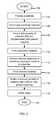
- FIG. 2is a simplified process flow diagram illustrating a method of patterning a thin film photovoltaic panel according to an embodiment of the present invention.
- FIG. 3-10are simplified diagrams illustrating a method of patterning a thin film photovoltaic panel according to an embodiment of the present invention.
- Embodiments according to the present inventionrelates to photovoltaic materials and manufacturing method. More particularly, the present invention provides a method and structure for patterning thin film photovoltaic panels with improved accuracy.
- the present method and structureinclude forming a first series of patterns with pre-compensated inter-pattern spacing followed by a second series of patterns after substrate compaction in thermal processing. The method is applied to a thin-film stack for manufacturing copper indium diselenide based thin film photovoltaic devices, but it would be recognized that the invention may have other configurations.
- FIG. 1Ashows a top view of a portion of a substrate from a first edge region 10 to a second edge region 30 on which a series of line patterns P 1 is formed.
- the inter-pattern spacing S between any neighboring patterns P 1is substantially the same.
- the patterns P 1are scribed into an electrode layer, for example, a molybdenum material to form a patterned structure. Over the patterned structure a photovoltaic absorber will be added.
- a typical method for forming the absorberincludes adding a precursor material and performing one or more thermal treatment processes during or after adding the precursor material.
- FIG. 1Bshows the same portion of patterned substrate panel after the one or more thermal treatment processes which may need to anneal the substrate up to a temperature approaching the glass strain point.
- the anneal pointmay be near 530 Degree Celsius.
- a thermally caused substrate compactionoccurs. For example, using the second edge region as a reference point, the first edge region of the substrate is shifted to from position 10 to position 20 .
- each of the series of line patterns P 1 within the patterned structureis shifted in position to a series of line patterns P′ 1 with a changed inter-pattern spacing (typically shrinks)
- the P 1 -P 1 spacing Sis changed to P′ 1 -P′ 1 spacing S′ after the one or more thermal process causing the substrate compaction.
- the glass materialfor example soda lime glass used for making a thin film photovoltaic panel, usually has isotropic physical properties so that the compaction may be substantially uniform throughout the substrate.
- the compaction parameterwhich is defined as a percentage change in dimension in this case is substantially a position independent constant.
- FIG. 1Cshows another series of line patterns P 2 are formed by the scribe device mentioned above.
- a pattern P 2is supposed to be scribed by disposing a tip to a location that shifts a lateral distance D away from a first pattern P 1 .
- the P 1 -P 1 spacing Schanges to P′ 1 -P′ 1 spacing S′, and S′ is smaller now than P 2 -P 2 spacing L.
- P 1 -P 2 spacing DFor example, using a pattern P 1 next to the first edge region 20 as a reference point a pattern P 2 is scribed at a distance D away from P 1 .
- Other P 2 patternsare multiple of L spaced away this pattern P 2 .
- the P 1 -P 2 spacingbecomes larger and larger (D′′>D′>D), causing extra spatial regions between those P 1 and P 2 which are wasted since they are not beneficial for photovoltaic function and correspondingly poor efficiency of the photovoltaic device.
- the changed P 1 -P 1 inter-pattern spacingmay result in a smaller and smaller P 1 -P 2 spacing, which increases possibility of electrical shorting of the electrical link and device failure.
- FIG. 2Bprovides an exemplary plot of P 1 -P 2 displacement versus its relative position on a sample substrate. All patterns are included across the substrate from left, middle, to right and the result shows a substantial linear relationship. The slope of the fitted line gives a value of the compaction parameter for this sample substrate panel, or eventually used as a reference parameter for all substrate panels from a same manufacture lot.
- the specific value of the compaction parameterdepends on the particular substrate material and its thermal history. For example, a typical soda lime glass substrate may be associated with a compaction parameter of about 500 ppm when the glass substrate has experienced a thermal annealing that approaches an anneal point of about 530 Degrees Celsius.
- FIG. 2Ais a simplified process flow diagram illustrating a method for patterning a thin film photovoltaic cell according to an embodiment of the present invention. As shown the method begins with a Start step (Step 102 ). The method includes providing a substrate (Step 104 ).
- the substratecan be a transparent material such as a glass. In a specific embodiment, a soda lime glass substrate is used. In particular, the substrate may be just one of many substrates from a same manufacturing lot having substantially the same thermal history.
- one or more sample substratescan be selected from the manufacturing lot to measure their geometric dimension before/after the one or more predetermined thermal processes, from which a compaction parameter associated with the substrate compaction can be determined. It is found that for soda lime glass the compaction parameter is substantially a constant for a particular manufacturing lot which is independent of position on the substrate. This means that the substrate compaction is substantially a uniform deformation where its dimension changes linearly.
- the amount of compactioncan be measured by a Dilatometer before/after it is subjected to the one or more thermal processes.
- the resultsindicate that a compaction parameter of a soda lime glass is between 500 ppm to 600 ppm for an anneal point of about 530° C.
- the compaction parametermay be position dependent so that the substrate changes non-linearly in dimension from a first edge to a second edge.
- the compaction parameter as a function of relative position on the substratecan be still pre-determined using a sample substrate subjecting to the corresponding thermal process.
- embodiments of the present methodfurther include forming a back electrode material overlying the substrate (Step 106 ).
- the back electrode materialcan be provided by a conductive material including metal and transparent conductive oxide. In a specific embodiment a molybdenum film is formed. Other metal materials may also be used, depending on the application.
- the methodincludes forming a first plurality of patterns (Step 108 ) into the back electrode material with a pre-compensated inter-pattern spacing. The compaction parameter deduced earlier is used to determine a pattern position.
- the next patternis determined to be positioned at a standard distance (e.g., a predetermined cell dimension) away from the first pattern plus a pre-compensated shift proportional to the compaction parameter.
- a standard distancee.g., a predetermined cell dimension
- the above procedureis simply repeated.
- a first patterned structureis formed in the back electrode material overlying the substrate and is configured to have an inter-pattern spacing set to be bigger than a standard cell dimension as a compensation for upcoming substrate compaction.
- the pre-compensated inter-pattern spacingis still substantially uniform provided that the compaction parameter is a position-independent constant. If the compaction parameter is position dependent, the inter-pattern spacing may be adjusted for each pattern accordingly.
- focused laser beamis employed to perform the patterning for forming a first plurality of patterns with pre-compensated inter-pattern spacing, because the focused laser beam can be accurately positioned spatially so as to accomplish the spatial pre-compensation of the patterning process throughout the whole substrate panel.
- a precursor materialcan be formed overlying the back electrode material (Step 110 ), after the first plurality of patterns are formed in parallel having a first inter-pattern spacing proportionally expanded based on the compaction parameter from the first edge or the second edge of the substrate.
- the precursor materialincludes all materials needed for forming a photovoltaic absorber structure.
- the precursor materialincludes copper species, indium species, and/or gallium species. These precursor material species can be deposited at relative low temperature using sputtering technique or other thin film deposition method to form a composite film ready for being transformed into a photovoltaic absorber by additionally processes.
- the methodthen includes performing one or more thermal treatment processes to transform the precursor material to a absorber structure (Step 112 ).
- thisincludes a SAS (selenization and sulfurization) process by subjecting the substrate with the precursor material overlying the first patterned structure to an environment comprising selenium gaseous species and sulfur species. In that environment, the precursor material reacts with the selenium work gas under a predetermined temperature ramping profile.
- the resulted photovoltaic absorber structurecomprises a p-type copper-indium-diselenide compound semiconductor with multi-grain chalcopyrite structure.
- a window materialcan be added overlying the absorber structure (Step 114 ).
- the window materialincludes cadmium sulfide material.
- the window materialcan be made of transparent oxide with desired n-type doping levels. More details about the formation of the absorber structure by applying the SAS thermal treatment process to a precursor material under a predetermined temperature profile and subsequent window material formation can be found in U.S. Patent application No. 61/101,635, titled “LARGE SCALE METHOD AND FURNACE SYSTEM FOR SELENIZATION OF THIN FILM PHOTOVOLTAIC MATERIALS” filed on Sep. 30, 2008 by Robert Wieting, commonly assigned and incorporated for references for all purposes.
- embodiments of present inventionprovide a self-compensation mechanism for the first plurality of patterns after the SAS process. Since the first plurality of patterns has been pre-compensated in each of their positions when scribed using a properly positioned focused laser beam before the SAS process, the substrate compaction effect during the SAS thermal process causes the inter-pattern spacing to return to substantially the standard cell dimension predetermined for the thin film photovoltaic device on the substrate panel. Furthermore, the method for patterning the thin film photovoltaic device includes forming a second plurality of patterns (Step 116 ) through the window material and absorber structure.
- Each of the second plurality of patternsis one-to-one associated with each of the first plurality of patterns formed in Step 108 for each strip shaped cell designed with a standard cell spatial dimension on the substrate panel.
- the second plurality of patternscan be conveniently formed using a scribe device having multiple mechanical tips. For example four or more tips with equal tip-tip spacing can be installed to the scribe device.
- a pivoted armcan be configured to apply controllable pressure force to each tip for scribing and removing a portion of film material.
- the tipis composed of a proper material that is capable to remove a certain amount of film material when a proper force and a proper scanning speed are applied to the scribe device.
- the tip-tip spacingis chosen for making the desired inter-pattern spacing for the second plurality of patterns.
- the scribe deviceis disposed so that each tip is in a desired location above the film (of window material and absorber structure). Specifically, the desired tip location is set to be shifted a predetermined distance away from a position of a particular one of the first plurality of patterns.
- one of the first patternssuch as the one located near the first edge, can be chosen as a reference point to dispose tips of the scribe device.
- the second plurality of patternscan be scribed conveniently in multiplication with each pattern having a predetermined displacement from any one of the first plurality of patterns. Additionally, the P 1 -P 2 displacement is substantially uniform across the whole substrate.
- a top electrode materialcan also be formed overlying the window material and filling the recessed portion of the second patterns.
- the methodfurther performs other steps to complete the photovoltaic device (Step 116 ). These other steps may include providing interconnect elements, ribbon elements, lamination, and framing among others to complete the photovoltaic panel device.
- the methodends with an end step (Step 118 ). Of course there can be other variations, modifications, and alternatives.
- the above sequence of stepsprovides a method of patterning and forming a photovoltaic device according to an embodiment of the present invention.
- the methodincludes a step of patterning an absorber structure and a window material using a scribe device according to a specific embodiment.
- one or more stepsmay be added, one or more steps may be eliminated, and one or more steps may be performed in a different sequence without departing from the scope of the claims herein.
- a third plurality of patternsmay be performed using substantially the same scribe device having multiple mechanical tips.
- the tip-tip spacingcan be substantially the same as that set for scribing the second plurality of patterns because it still represents a standard cell spatial dimension.
- each of the third plurality of patternscan be shifted a (different) predetermined distance away from a corresponding one of the second plurality of patterns.
- each cellcontains a set of three patterns that respectively serves as a structural element for forming the electric contact of the particular photovoltaic cell.
- a plurality of those cellsis in stripe shape distributed from the first edge to the second edge.
- FIGS. 3-10are simplified diagrams illustrating a method for patterning a thin film photovoltaic panel according to an embodiment of the present invention. These diagrams are merely examples and should not unduly limit the claims herein. One skilled in the art would recognize other variations, modifications, and alternatives.
- a substrate panel 100is provided and overlaid by a back electrode layer 101 .
- the substrate panel 100can be a glass material such as soda lime glass in an embodiment. Soda lime glass is a cost effective option for a transparent substrate for manufacturing thin film photovoltaic devices. Other suitable transparent substrates such as quartz, fused silica or solar glass can also be used.
- the substrate panel 100has been characterized by a compaction parameter associated with a specific substrate material subjected to a specific thermal annealing point and can be determined using one or more sample substrates selected from a group of substrates out of a same manufacturing lot with similar thermal history.
- the sample substrateis subjected to one or more thermal processes having at least an anneal approaching its glass strain point.
- a dilatometercan be used for measuring a series of length scale of the substrate panel to determine the degree of compaction characterized by a compaction parameter.
- the substrate compactionis expected to be substantially linear or uniform.
- the compaction parameteris a substrate deformation ratio, a substantially position-independent constant.
- a value of about 500 to 600 ppmis obtained for typical soda lime glass in a process with substrate temperature approaching 530° C.
- a spatial contractionwould be subjected to the same compaction parameter.
- the compaction parametermay be either different in value or be a function of position of the substrate. For latter situation, the spatial deformation becomes position-dependent based on the function.
- the back electrode material 101 overlying the transparent substrate panel 100may be selected from a transparent conductor oxide (TCO) such as indium tin oxide (commonly called ITO), fluorine doped tin oxide, and a metal material including molybdenum material in a specific embodiment.
- TCOtransparent conductor oxide
- ITOindium tin oxide
- fluorine doped tin oxidefluorine doped tin oxide
- metal material including molybdenum materialin a specific embodiment.
- the molybdenum materialcan be formed using deposition techniques such as sputtering, plating, physical vapor deposition (including evaporation, sublimation), chemical vapor deposition (including plasma enhanced processes) following by a patterning process.
- Molybdenum materialprovides certain advantage over other electrode material for copper indium diselenide (CIS) or copper indium gallium diselenide (CIGS) based thin film photovoltaic cells.
- molybdenum materialprovides a low contact resistance for CIGS film and stability over subsequent process steps.
- molybdenum materialis formed by depositing a first molybdenum layer overlying the transparent substrate member.
- the first molybdenum layerhas a first thickness and a tensile characteristic in a specific embodiment.
- a second molybdenum layer having a compression characteristics and a second thicknessis formed overlying the first molybdenum layer.
- the first electrode layer comprising the molybdenum materialcan be further patterned as shown. Further details of deposition and patterning of the molybdenum material can be found at least in U.S. Provision Application No. 61/101,646 filed Sep. 30, 2008 and U.S. Provision Application No. 61/101,650 filed Sep. 30, 2008, commonly assigned, and hereby incorporate by reference.
- the methodincludes forming a first plurality of patterns P 1 into the back electrode material 101 overlying a portion of the substrate 100 from a first edge region 10 to a second edge region 30 .
- the positioning of each of the first plurality of patterns P 1is pre-compensated using the compaction parameter obtained earlier for this (type of) substrate.
- the inter-pattern spacing S 0 of P 1is intentionally expanded from a base (standard) spacing plus an extra distance based on the compaction parameter. For example, if a standard cell dimension is 6.1 mm, it is expected to be equal to the inter-pattern spacing.
- This inter-pattern spacing precompensationis executed through out all first plurality of patterns P 1 from the first edge region 10 to the second edge region 30 . In the end, a first patterned structure P 1 s is formed overlying the substrate panel.
- the compaction parameteris more complicated (depending on substrate material) and may be a function of position on the substrate.
- the precompensation of the first plurality of patterns P 1needs to be adjusted accordingly so that the inter-pattern spacing may not be a constant but a changed value from the first edge region to the second edge region one after another.
- the patterning of the first plurality of patterns P 1can be performed using a focused laser beam which can be positioned to a desired position with high accuracy and easily controlled in spot re-positioning and beam scanning.
- the first plurality of patterns P 1comprises a recessed region for each pattern and will be used form back electrode contact for the photovoltaic cells. Over the back electrode material a photovoltaic absorber is to be formed.
- a precursor material 103is added overlying the electrode material 101 . As shown in the cross-sectional view of FIG. 5 , the precursor material 103 has fully covered the first patterned structure P 1 s, which comprises the first plurality of patterns P 1 embedded within the back electrode material 101 .
- the precursor materialin an embodiment, comprises copper species, indium species, and optionally gallium species deposited via sputtering techniques.
- Embodiments of the methodprovides one or more thermal treatment processes to transform the precursor material into an absorber structure.
- the substrate 100 covered with the precursor material 103 and embedded first plurality of patterns in the back electrode material 101can be loaded to a chamber comprising a gaseous environment of selenium species and/or sulfur species and/or one or more inert work gases.
- the substratethen is subjected to one or more thermal processes 200 having a predetermined temperature profile comprising one or more ramping-up, holding, ramping-down stages to induce a reactive annealing of the precursor material 103 at desired temperatures for certain periods. At least in a certain stage the substrate temperature may approach the glass strain point of about 530° C.
- the precursor material 103 with copper, indium, or gallium speciesis reacted with selenium species at elevated temperatures and subsequently annealed through temperatures ramping up and down and finally transformed to an absorber 105 comprising a copper-indium-gallium-diselenide compound semiconductor with chalcopyrite structure grains.
- the temperature profile associated with the one or more reactive thermal treatment processes 200is substantially the same experienced by the bare sample substrate (similar to substrate 100 ) for determining the compaction parameter. Therefore, after the one or more thermal treatment processes the precursor material is transformed to absorber structure and at the same time the first plurality of patterns P 1 is relatively re-positioned due to a compaction of the substrate 100 . Shown in FIG.
- the substrate compactioncauses the first edge region of the substrate 100 to shift from position 10 to position 20 during the one or more thermal processes 200 . Accordingly, since the line patterns P 1 have been pre-compensated by proportionally expanding each inter-pattern spacing from a base value, the compaction process re-positions each of the patterns P 1 to yield a second patterned structure with a second inter-pattern spacing S 1 substantially throughout the first plurality of patterns.
- FIG. 7shows a top view of the panel wherein the second patterned P 1 structure formed after the one or more thermal treatment processes is embedded within the back electrode material 103 . Now the second patterned structure comprises the first plurality of patterns P 1 but with the inter-pattern spacing S 1 . For example, after going through the processes 200 the inter-pattern spacing S 1 is substantially equal to about 6.1 mm designed for each strip shaped cell on a CIGS thin film photovoltaic panel.
- the methodfurther includes forming a window material 107 overlying the absorber structure 105 to form a light conversion function film for photovoltaic cells on the substrate panel, shown in FIG. 8 .
- the window material 107is often provided using a wide bandgap n-type semiconductor material for a p-type absorber structure 105 in a specific embodiment.
- the window materialuses a cadmium sulfide overlying absorber structure comprising CIGS, CIS and related materials.
- the window materialcan be deposited using techniques such as sputtering, vacuum evaporation, chemical bath deposition, among others.
- the methodfurther includes patterning the photovoltaic function film for each cell.
- a mechanical scribing devicecan be applied to perform the patterning process.
- the mechanical scribing device 300can include multiple tips 301 or scribe head having an equal spacing L so that one scribing action can provide patterning for multiple cells, wherein the spacing L is simply the designed standard cell spatial dimension, for example, 6.1 mm.
- each tip 301can be made of material such as diamond, tungsten carbide, or silicon carbide, and the like. Other materials having sufficient hardness may also be used for the tip depending on the application.
- the tip 301is also characterized by a radius ranging from about 20 microns to about 40 microns and preferably 25 microns and more.
- the scribe device 300can be a pivot device in a specific embodiment which also connects to a control device to positioning the tips and applying the desired force to the tips in a certain range of angles to form recessed patterns into the film (including window material 107 and absorber structure 105 ).
- FIG. 9shows a side view of a portion of the substrate panel with a second plurality of patterns P 2 (one for each cell) scribed by the mechanical scribe device 300 using equally spaced multiple tips.
- the depth of the recessed patternis substantially equal or slightly greater than the thickness of combined window material and absorber structure.
- the recessed regionis not surpassed 200 Angstrom into the molybdenum material under the absorber structure.
- each of the second plurality of patterns P 2is designated to be a predetermined distance D away from corresponding one of the first plurality of patterns P 1 for each cell.
- FIG. 10a top view to see relative positions across the portion of the substrate from the first edge region 20 to the second edge region 30 .
- the first plurality of patterns P 1created with pre-compensated positions, have been re-positioned after the thermal treatment process to give an inter-pattern spacing S 1 substantially equal to the standard cell dimension.
- the tip-tip spacing L of the scribe deviceis configured to form second plurality of patterns P 2 for fitting each cell in the designed cell spatial dimension. Therefore, L is substantially the same as S 1 .
- the shifted distance D of P 2 relative to P 1 , or the P 1 -P 2 spacingwould be also substantially a constant for all cells throughout the panel.
- Embodiments of the present invention using a precompensated P 1substantially help to reduce the occurrence of an enlarged P 1 -P 2 spacing after the thermal treatment processes for forming absorber structure.
- the region between patterns P 1 and P 2essentially cannot be used for directly converting photons to electrons, it needs to be kept small but a constant.
- Embodiments of the present inventionthus prevent any un-desired enlargement of P 1 -P 2 area. This directly translates to an enhancement in cell efficiency for the photovoltaic panel.
- embodiments of the present inventionalso reduce the potential risk of un-desired P 1 -P 2 shorting due to the substrate compaction, enhancing the device reliability.
- Embodiments of the present inventioncan be applied further for patterning additional series of patterns P 3 or others using the same scribe device 300 having multiple mechanical tips.
- another transparent conductive materialsuch as TZO material or ITO material can be added using techniques such as sputtering, physical vapor deposition, solution based deposition, MOCVD and others.
- a third plurality of patterns P 3can be formed with each pattern P 3 at a proper lateral distance away from P 2 (and of course, some lateral distance away from P 1 ) for each cell on the whole panel.
- the inter-pattern spacing of the third plurality of patterns P 3can be substantially the same value L or S 1 , i.e., the same as the standard cell dimension.
- FIG. 10shows an exemplary top view of the panel with many cells and each with three sets of patterns respectively with a proper position and spacing.
- the present methodcan also be applied to silicon based photovoltaic devices. It is understood that the examples and embodiments described herein are for illustrative purposes only and that various modifications or changes in light thereof will be suggested to persons skilled in the art and are to be included within the spirit and purview of this application and scope of the appended claims.
Landscapes
- Photovoltaic Devices (AREA)
Abstract
Description
Claims (18)
Priority Applications (1)
| Application Number | Priority Date | Filing Date | Title |
|---|---|---|---|
| US13/006,710US8263494B2 (en) | 2010-01-25 | 2011-01-14 | Method for improved patterning accuracy for thin film photovoltaic panels |
Applications Claiming Priority (2)
| Application Number | Priority Date | Filing Date | Title |
|---|---|---|---|
| US29818510P | 2010-01-25 | 2010-01-25 | |
| US13/006,710US8263494B2 (en) | 2010-01-25 | 2011-01-14 | Method for improved patterning accuracy for thin film photovoltaic panels |
Publications (2)
| Publication Number | Publication Date |
|---|---|
| US20110256661A1 US20110256661A1 (en) | 2011-10-20 |
| US8263494B2true US8263494B2 (en) | 2012-09-11 |
Family
ID=44788493
Family Applications (1)
| Application Number | Title | Priority Date | Filing Date |
|---|---|---|---|
| US13/006,710Expired - Fee RelatedUS8263494B2 (en) | 2010-01-25 | 2011-01-14 | Method for improved patterning accuracy for thin film photovoltaic panels |
Country Status (1)
| Country | Link |
|---|---|
| US (1) | US8263494B2 (en) |
Cited By (17)
| Publication number | Priority date | Publication date | Assignee | Title |
|---|---|---|---|---|
| US20100180927A1 (en)* | 2008-08-27 | 2010-07-22 | Stion Corporation | Affixing method and solar decal device using a thin film photovoltaic and interconnect structures |
| US20110020564A1 (en)* | 2008-06-11 | 2011-01-27 | Stion Corporation | Processing method for cleaning sulfur entities of contact regions |
| US8425739B1 (en) | 2008-09-30 | 2013-04-23 | Stion Corporation | In chamber sodium doping process and system for large scale cigs based thin film photovoltaic materials |
| US8435822B2 (en) | 2008-09-30 | 2013-05-07 | Stion Corporation | Patterning electrode materials free from berm structures for thin film photovoltaic cells |
| US8461061B2 (en) | 2010-07-23 | 2013-06-11 | Stion Corporation | Quartz boat method and apparatus for thin film thermal treatment |
| US8512528B2 (en) | 2007-11-14 | 2013-08-20 | Stion Corporation | Method and system for large scale manufacture of thin film photovoltaic devices using single-chamber configuration |
| US8617917B2 (en) | 2008-06-25 | 2013-12-31 | Stion Corporation | Consumable adhesive layer for thin film photovoltaic material |
| US8628997B2 (en) | 2010-10-01 | 2014-01-14 | Stion Corporation | Method and device for cadmium-free solar cells |
| US8673675B2 (en) | 2008-09-30 | 2014-03-18 | Stion Corporation | Humidity control and method for thin film photovoltaic materials |
| US8809096B1 (en) | 2009-10-22 | 2014-08-19 | Stion Corporation | Bell jar extraction tool method and apparatus for thin film photovoltaic materials |
| US8859880B2 (en) | 2010-01-22 | 2014-10-14 | Stion Corporation | Method and structure for tiling industrial thin-film solar devices |
| US8871305B2 (en) | 2007-06-29 | 2014-10-28 | Stion Corporation | Methods for infusing one or more materials into nano-voids of nanoporous or nanostructured materials |
| US8928105B2 (en) | 2010-05-28 | 2015-01-06 | Flisom Ag | Method and apparatus for thin film module with dotted interconnects and vias |
| US8941132B2 (en) | 2008-09-10 | 2015-01-27 | Stion Corporation | Application specific solar cell and method for manufacture using thin film photovoltaic materials |
| US9096930B2 (en) | 2010-03-29 | 2015-08-04 | Stion Corporation | Apparatus for manufacturing thin film photovoltaic devices |
| US10096731B2 (en) | 2014-01-31 | 2018-10-09 | Flisom Ag | Method for thin-film via segments in photovoltaic device |
| WO2023082016A1 (en)* | 2021-11-15 | 2023-05-19 | Necula Robert | Thin film photovoltaic devices and manufacturing methods |
Citations (198)
| Publication number | Priority date | Publication date | Assignee | Title |
|---|---|---|---|---|
| US3520732A (en) | 1965-10-22 | 1970-07-14 | Matsushita Electric Industrial Co Ltd | Photovoltaic cell and process of preparation of same |
| US3975211A (en) | 1975-03-28 | 1976-08-17 | Westinghouse Electric Corporation | Solar cells and method for making same |
| US4062038A (en) | 1976-01-28 | 1977-12-06 | International Business Machines Corporation | Radiation responsive device |
| US4332974A (en) | 1979-06-28 | 1982-06-01 | Chevron Research Company | Multilayer photovoltaic cell |
| US4335266A (en) | 1980-12-31 | 1982-06-15 | The Boeing Company | Methods for forming thin-film heterojunction solar cells from I-III-VI.sub.2 |
| DE3314197A1 (en) | 1982-04-28 | 1983-11-03 | Energy Conversion Devices, Inc., 48084 Troy, Mich. | P-CONDUCTING AMORPHOUS SILICON ALLOY WITH A LARGE BAND GAP AND MANUFACTURING PROCESS THEREFOR |
| US4441113A (en) | 1981-02-13 | 1984-04-03 | Energy Conversion Devices, Inc. | P-Type semiconductor material having a wide band gap |
| US4442310A (en) | 1982-07-15 | 1984-04-10 | Rca Corporation | Photodetector having enhanced back reflection |
| US4461922A (en) | 1983-02-14 | 1984-07-24 | Atlantic Richfield Company | Solar cell module |
| US4465575A (en) | 1981-09-21 | 1984-08-14 | Atlantic Richfield Company | Method for forming photovoltaic cells employing multinary semiconductor films |
| US4471155A (en) | 1983-04-15 | 1984-09-11 | Energy Conversion Devices, Inc. | Narrow band gap photovoltaic devices with enhanced open circuit voltage |
| US4499658A (en) | 1983-09-06 | 1985-02-19 | Atlantic Richfield Company | Solar cell laminates |
| US4507181A (en) | 1984-02-17 | 1985-03-26 | Energy Conversion Devices, Inc. | Method of electro-coating a semiconductor device |
| US4517403A (en) | 1983-05-16 | 1985-05-14 | Atlantic Richfield Company | Series connected solar cells and method of formation |
| US4518855A (en) | 1982-09-30 | 1985-05-21 | Spring-Mornne, Inc. | Method and apparatus for statically aligning shafts and monitoring shaft alignment |
| US4532372A (en) | 1983-12-23 | 1985-07-30 | Energy Conversion Devices, Inc. | Barrier layer for photovoltaic devices |
| US4542255A (en) | 1984-01-03 | 1985-09-17 | Atlantic Richfield Company | Gridded thin film solar cell |
| US4581108A (en) | 1984-01-06 | 1986-04-08 | Atlantic Richfield Company | Process of forming a compound semiconductive material |
| US4589194A (en) | 1983-12-29 | 1986-05-20 | Atlantic Richfield Company | Ultrasonic scribing of thin film solar cells |
| US4598306A (en) | 1983-07-28 | 1986-07-01 | Energy Conversion Devices, Inc. | Barrier layer for photovoltaic devices |
| US4599154A (en) | 1985-03-15 | 1986-07-08 | Atlantic Richfield Company | Electrically enhanced liquid jet processing |
| US4611091A (en) | 1984-12-06 | 1986-09-09 | Atlantic Richfield Company | CuInSe2 thin film solar cell with thin CdS and transparent window layer |
| US4623601A (en) | 1985-06-04 | 1986-11-18 | Atlantic Richfield Company | Photoconductive device containing zinc oxide transparent conductive layer |
| US4625070A (en) | 1985-08-30 | 1986-11-25 | Atlantic Richfield Company | Laminated thin film solar module |
| US4638111A (en) | 1985-06-04 | 1987-01-20 | Atlantic Richfield Company | Thin film solar cell module |
| US4661370A (en) | 1984-02-08 | 1987-04-28 | Atlantic Richfield Company | Electric discharge processing of thin films |
| US4663495A (en) | 1985-06-04 | 1987-05-05 | Atlantic Richfield Company | Transparent photovoltaic module |
| US4705912A (en) | 1985-09-27 | 1987-11-10 | Sanyo Electric Co., Ltd. | Photovoltaic device |
| US4724011A (en) | 1983-05-16 | 1988-02-09 | Atlantic Richfield Company | Solar cell interconnection by discrete conductive regions |
| US4727047A (en) | 1980-04-10 | 1988-02-23 | Massachusetts Institute Of Technology | Method of producing sheets of crystalline material |
| US4751149A (en) | 1985-06-04 | 1988-06-14 | Atlantic Richfield Company | Chemical vapor deposition of zinc oxide films and products |
| US4775425A (en) | 1987-07-27 | 1988-10-04 | Energy Conversion Devices, Inc. | P and n-type microcrystalline semiconductor alloy material including band gap widening elements, devices utilizing same |
| US4798660A (en) | 1985-07-16 | 1989-01-17 | Atlantic Richfield Company | Method for forming Cu In Se2 films |
| US4816082A (en) | 1987-08-19 | 1989-03-28 | Energy Conversion Devices, Inc. | Thin film solar cell including a spatially modulated intrinsic layer |
| US4873118A (en) | 1988-11-18 | 1989-10-10 | Atlantic Richfield Company | Oxygen glow treating of ZnO electrode for thin film silicon solar cell |
| US4915745A (en) | 1988-09-22 | 1990-04-10 | Atlantic Richfield Company | Thin film solar cell and method of making |
| US4950615A (en) | 1989-02-06 | 1990-08-21 | International Solar Electric Technology, Inc. | Method and making group IIB metal - telluride films and solar cells |
| US4968354A (en) | 1987-11-09 | 1990-11-06 | Fuji Electric Co., Ltd. | Thin film solar cell array |
| US4996108A (en) | 1989-01-17 | 1991-02-26 | Simon Fraser University | Sheets of transition metal dichalcogenides |
| US5008062A (en) | 1988-01-20 | 1991-04-16 | Siemens Solar Industries, L.P. | Method of fabricating photovoltaic module |
| US5011565A (en) | 1989-12-06 | 1991-04-30 | Mobil Solar Energy Corporation | Dotted contact solar cell and method of making same |
| US5028274A (en) | 1989-06-07 | 1991-07-02 | International Solar Electric Technology, Inc. | Group I-III-VI2 semiconductor films for solar cell application |
| US5039353A (en) | 1989-04-27 | 1991-08-13 | Societe Dite: Solems (Societe Anonyme) | Process for improving the spectral response of a photoconductive structure, and improved solar cell and photoreceptive structure |
| US5045409A (en) | 1987-11-27 | 1991-09-03 | Atlantic Richfield Company | Process for making thin film solar cell |
| US5078803A (en) | 1989-09-22 | 1992-01-07 | Siemens Solar Industries L.P. | Solar cells incorporating transparent electrodes comprising hazy zinc oxide |
| US5125984A (en) | 1990-05-31 | 1992-06-30 | Siemens Aktiengesellschaft | Induced junction chalcopyrite solar cell |
| US5133809A (en) | 1989-10-07 | 1992-07-28 | Showa Shell Sekiyu K.K. | Photovoltaic device and process for manufacturing the same |
| US5137835A (en) | 1990-07-24 | 1992-08-11 | Siemens Aktiengesellschaft | Method for manufacturing a chalcopyrite solar cell |
| US5154777A (en) | 1990-02-26 | 1992-10-13 | Mcdonnell Douglas Corporation | Advanced survivable space solar power system |
| US5180686A (en) | 1988-10-31 | 1993-01-19 | Energy Conversion Devices, Inc. | Method for continuously deposting a transparent oxide material by chemical pyrolysis |
| US5211824A (en) | 1991-10-31 | 1993-05-18 | Siemens Solar Industries L.P. | Method and apparatus for sputtering of a liquid |
| US5217564A (en) | 1980-04-10 | 1993-06-08 | Massachusetts Institute Of Technology | Method of producing sheets of crystalline material and devices made therefrom |
| US5231047A (en) | 1991-12-19 | 1993-07-27 | Energy Conversion Devices, Inc. | High quality photovoltaic semiconductor material and laser ablation method of fabrication same |
| US5248345A (en) | 1990-10-17 | 1993-09-28 | Showa Shell Sekiyu K.K. | Integrated photovoltaic device |
| US5261968A (en) | 1992-01-13 | 1993-11-16 | Photon Energy, Inc. | Photovoltaic cell and method |
| US5298086A (en) | 1992-05-15 | 1994-03-29 | United Solar Systems Corporation | Method for the manufacture of improved efficiency tandem photovoltaic device and device manufactured thereby |
| US5336623A (en) | 1992-03-02 | 1994-08-09 | Showa Shell Sekiyu K.K. | Process for producing integrated solar cell |
| US5346853A (en) | 1992-06-29 | 1994-09-13 | United Solar Systems Corporation | Microwave energized deposition process with substrate temperature control for the fabrication of P-I-N photovoltaic devices |
| US5397401A (en) | 1992-06-29 | 1995-03-14 | Canon Kabushiki Kaisha | Semiconductor apparatus covered with a sealing resin composition |
| US5445847A (en) | 1992-05-19 | 1995-08-29 | Matsushita Electric Industrial Co., Ltd. | Method for preparing chalcopyrite-type compound |
| US5474939A (en) | 1992-12-30 | 1995-12-12 | Siemens Solar Industries International | Method of making thin film heterojunction solar cell |
| US5501744A (en) | 1992-01-13 | 1996-03-26 | Photon Energy, Inc. | Photovoltaic cell having a p-type polycrystalline layer with large crystals |
| US5512107A (en) | 1992-03-19 | 1996-04-30 | Siemens Solar Gmbh | Environmentally stable thin-film solar module |
| US5528397A (en) | 1991-12-03 | 1996-06-18 | Kopin Corporation | Single crystal silicon transistors for display panels |
| US5536333A (en) | 1992-05-12 | 1996-07-16 | Solar Cells, Inc. | Process for making photovoltaic devices and resultant product |
| US5578103A (en) | 1994-08-17 | 1996-11-26 | Corning Incorporated | Alkali metal ion migration control |
| US5578503A (en) | 1992-09-22 | 1996-11-26 | Siemens Aktiengesellschaft | Rapid process for producing a chalcopyrite semiconductor on a substrate |
| US5622634A (en) | 1993-12-17 | 1997-04-22 | Canon Kabushiki Kaisha | Method of manufacturing electron-emitting device, electron source and image-forming apparatus |
| US5626688A (en) | 1994-12-01 | 1997-05-06 | Siemens Aktiengesellschaft | Solar cell with chalcopyrite absorber layer |
| US5665175A (en) | 1990-05-30 | 1997-09-09 | Safir; Yakov | Bifacial solar cell |
| US5676766A (en) | 1993-09-30 | 1997-10-14 | Siemens Aktiengesellschaft | Solar cell having a chalcopyrite absorber layer |
| US5726065A (en) | 1995-02-21 | 1998-03-10 | Imec Vzw | Method of preparing solar cell front contacts |
| US5738731A (en) | 1993-11-19 | 1998-04-14 | Mega Chips Corporation | Photovoltaic device |
| US5868869A (en) | 1995-06-07 | 1999-02-09 | Photon Energy, Inc. | Thin film photovoltaic device and process of manufacture |
| US5977476A (en) | 1996-10-16 | 1999-11-02 | United Solar Systems Corporation | High efficiency photovoltaic device |
| US5981868A (en) | 1996-10-25 | 1999-11-09 | Showa Shell Sekiyu K.K. | Thin-film solar cell comprising thin-film light absorbing layer of chalcopyrite multi-element compound semiconductor |
| US5985691A (en) | 1997-05-16 | 1999-11-16 | International Solar Electric Technology, Inc. | Method of making compound semiconductor films and making related electronic devices |
| US6040521A (en) | 1996-11-08 | 2000-03-21 | Showa Shell Sekiyu K.K. | N-type window layer for a thin film solar cell and method of making |
| US6048442A (en) | 1996-10-25 | 2000-04-11 | Showa Shell Sekiyu K.K. | Method for producing thin-film solar cell and equipment for producing the same |
| JP2000173969A (en) | 1998-12-03 | 2000-06-23 | Canon Inc | Rinse method and photovoltaic device |
| JP2000219512A (en) | 1998-11-24 | 2000-08-08 | Canon Inc | Method for manufacturing zinc oxide thin film, method for manufacturing photovoltaic device using the same, and photovoltaic device |
| US6107562A (en) | 1998-03-24 | 2000-08-22 | Matsushita Electric Industrial Co., Ltd. | Semiconductor thin film, method for manufacturing the same, and solar cell using the same |
| US6127202A (en) | 1998-07-02 | 2000-10-03 | International Solar Electronic Technology, Inc. | Oxide-based method of making compound semiconductor films and making related electronic devices |
| US6166319A (en) | 1997-08-01 | 2000-12-26 | Canon Kabushiki Kaisha | Multi-junction photovoltaic device with microcrystalline I-layer |
| US6172297B1 (en) | 1997-09-23 | 2001-01-09 | Institut Fur Solarenergieforschung Gmbh | Solar cell and method for fabrication of a solar cell |
| US6258620B1 (en) | 1997-10-15 | 2001-07-10 | University Of South Florida | Method of manufacturing CIGS photovoltaic devices |
| WO2001057932A1 (en) | 2000-02-07 | 2001-08-09 | Cis Solartechnik Gmbh | Flexible metal substrate for cis solar cells, and method for producing the same |
| US6294274B1 (en) | 1998-11-16 | 2001-09-25 | Tdk Corporation | Oxide thin film |
| US6307148B1 (en) | 1999-03-29 | 2001-10-23 | Shinko Electric Industries Co., Ltd. | Compound semiconductor solar cell and production method thereof |
| US6328871B1 (en) | 1999-08-16 | 2001-12-11 | Applied Materials, Inc. | Barrier layer for electroplating processes |
| US20020004302A1 (en) | 1995-09-14 | 2002-01-10 | Yoshihiko Fukumoto | Method for fabricating semiconductor device |
| US20020002992A1 (en) | 1998-06-30 | 2002-01-10 | Toshimitsu Kariya | Photovoltaic element |
| US6361718B1 (en) | 1998-02-05 | 2002-03-26 | Nippon Sheet Glass Co., Ltd. | Article having uneven surface, production process for the article, and composition for the process |
| US6372538B1 (en) | 2000-03-16 | 2002-04-16 | University Of Delaware | Fabrication of thin-film, flexible photovoltaic module |
| US20020061361A1 (en) | 2000-09-06 | 2002-05-23 | Hiroki Nakahara | Method and apparatus for fabricating electro-optical device and method and apparatus for fabricating liquid crystal panel |
| US20020063065A1 (en) | 2000-09-19 | 2002-05-30 | Yuichi Sonoda | Method of forming zinc oxide film and process for producing photovoltaic device using it |
| JP2002167695A (en) | 2000-09-19 | 2002-06-11 | Canon Inc | Method for forming zinc oxide film and method for manufacturing photovoltaic element using the same |
| US6423565B1 (en) | 2000-05-30 | 2002-07-23 | Kurt L. Barth | Apparatus and processes for the massproduction of photovotaic modules |
| DE10104726A1 (en) | 2001-02-02 | 2002-08-08 | Siemens Solar Gmbh | Process for structuring an oxide layer applied to a carrier material |
| JP2002270871A (en) | 2001-03-12 | 2002-09-20 | Canon Inc | Semiconductor element and method of forming silicon-based thin film |
| JP2002299670A (en) | 2001-04-03 | 2002-10-11 | Canon Inc | Silicon based thin film and photovoltaic device |
| US20030075717A1 (en) | 2001-03-12 | 2003-04-24 | Takaharu Kondo | Semiconductor element, and method of forming silicon-based film |
| US20030089899A1 (en) | 2000-08-22 | 2003-05-15 | Lieber Charles M. | Nanoscale wires and related devices |
| US6632113B1 (en) | 1998-09-09 | 2003-10-14 | Canon Kabushiki Kaisha | Image display apparatus, disassembly processing method therefor, and component recovery method |
| US6635307B2 (en) | 2001-12-12 | 2003-10-21 | Nanotek Instruments, Inc. | Manufacturing method for thin-film solar cells |
| US6653701B1 (en) | 1999-03-09 | 2003-11-25 | Fuji Xerox Co., Ltd. | Semiconductor device and production method thereof |
| US6667492B1 (en) | 1997-11-10 | 2003-12-23 | Don L. Kendall | Quantum ridges and tips |
| US6690041B2 (en) | 2002-05-14 | 2004-02-10 | Global Solar Energy, Inc. | Monolithically integrated diodes in thin-film photovoltaic devices |
| US6692820B2 (en) | 1998-08-19 | 2004-02-17 | The Trustees Of Princeton University | Organic photosensitive optoelectronic device with a charge blocking layer |
| US20040063320A1 (en) | 2002-09-30 | 2004-04-01 | Hollars Dennis R. | Manufacturing apparatus and method for large-scale production of thin-film solar cells |
| US20040084080A1 (en) | 2002-06-22 | 2004-05-06 | Nanosolar, Inc. | Optoelectronic device and fabrication method |
| US20040095658A1 (en) | 2002-09-05 | 2004-05-20 | Nanosys, Inc. | Nanocomposites |
| US6784492B1 (en) | 1991-03-18 | 2004-08-31 | Canon Kabushiki Kaisha | Semiconductor device including a gate-insulated transistor |
| US20040187917A1 (en) | 2003-03-29 | 2004-09-30 | Nanosolar, Inc. | Transparent electrode, optoelectronic apparatus and devices |
| JP2004332043A (en) | 2003-05-07 | 2004-11-25 | Canon Inc | Method and apparatus for forming zinc oxide thin film, and method for forming photovoltaic element |
| US20040245912A1 (en) | 2003-04-01 | 2004-12-09 | Innovalight | Phosphor materials and illumination devices made therefrom |
| US20040252488A1 (en) | 2003-04-01 | 2004-12-16 | Innovalight | Light-emitting ceiling tile |
| US20040256001A1 (en) | 2002-12-17 | 2004-12-23 | General Electric Company | Photovoltaic cell using stable cu2o nanocrystals and conductive polymers |
| WO2005011002A1 (en) | 2003-07-24 | 2005-02-03 | Kaneka Corporation | Silicon based thin film solar cell |
| US6852920B2 (en) | 2002-06-22 | 2005-02-08 | Nanosolar, Inc. | Nano-architected/assembled solar electricity cell |
| US20050074915A1 (en) | 2001-07-13 | 2005-04-07 | Tuttle John R. | Thin-film solar cell fabricated on a flexible metallic substrate |
| US6878871B2 (en) | 2002-09-05 | 2005-04-12 | Nanosys, Inc. | Nanostructure and nanocomposite based compositions and photovoltaic devices |
| US20050098205A1 (en) | 2003-05-21 | 2005-05-12 | Nanosolar, Inc. | Photovoltaic devices fabricated from insulating nanostructured template |
| US20050164432A1 (en) | 2000-08-22 | 2005-07-28 | President And Fellows Of Harvard College | Doped elongated semiconductors, growing such semiconductors, devices including such semiconductors and fabricating such devices |
| US20050194036A1 (en) | 2004-03-01 | 2005-09-08 | Basol Bulent M. | Low cost and high throughput deposition methods and apparatus for high density semiconductor film growth |
| JP2005311292A (en) | 2004-03-25 | 2005-11-04 | Kaneka Corp | Substrate for thin film solar cell, manufacturing method therefor, and thin film solar cell using the same |
| US20050287717A1 (en) | 2004-06-08 | 2005-12-29 | Nanosys, Inc. | Methods and devices for forming nanostructure monolayers and devices including such monolayers |
| US20060034065A1 (en) | 2004-08-10 | 2006-02-16 | Innovalight, Inc. | Light strips for lighting and backlighting applications |
| US20060040103A1 (en) | 2004-06-08 | 2006-02-23 | Nanosys, Inc. | Post-deposition encapsulation of nanostructures: compositions, devices and systems incorporating same |
| US20060051505A1 (en) | 2004-06-18 | 2006-03-09 | Uwe Kortshagen | Process and apparatus for forming nanoparticles using radiofrequency plasmas |
| US20060096635A1 (en) | 2004-11-10 | 2006-05-11 | Daystar Technologies, Inc. | Pallet based system for forming thin-film solar cells |
| US20060096536A1 (en) | 2004-11-10 | 2006-05-11 | Daystar Technologies, Inc. | Pressure control system in a photovoltaic substrate deposition apparatus |
| US20060096537A1 (en) | 2004-11-10 | 2006-05-11 | Daystar Technologies, Inc. | Method and apparatus for forming a thin-film solar cell using a continuous process |
| US20060112983A1 (en) | 2004-11-17 | 2006-06-01 | Nanosys, Inc. | Photoactive devices and components with enhanced efficiency |
| US20060130890A1 (en) | 2004-12-20 | 2006-06-22 | Palo Alto Research Center Incorporated. | Heterojunction photovoltaic cell |
| US20060160261A1 (en) | 2005-01-20 | 2006-07-20 | Nanosolar, Inc. | Series interconnected optoelectronic device module assembly |
| US20060174932A1 (en) | 2003-07-14 | 2006-08-10 | Hiroki Usui | Electrolyte compositon, photoelectric converter and dye-sensitized solar cell using same |
| US20060219288A1 (en) | 2004-11-10 | 2006-10-05 | Daystar Technologies, Inc. | Process and photovoltaic device using an akali-containing layer |
| US20060220059A1 (en) | 2003-04-09 | 2006-10-05 | Matsushita Electric Industrial Co., Ltd | Solar cell |
| US20060219547A1 (en) | 2004-11-10 | 2006-10-05 | Daystar Technologies, Inc. | Vertical production of photovoltaic devices |
| US7122398B1 (en) | 2004-03-25 | 2006-10-17 | Nanosolar, Inc. | Manufacturing of optoelectronic devices |
| US20060249202A1 (en) | 2004-09-20 | 2006-11-09 | Seunghyup Yoo | Photovoltaic cell |
| US20060267054A1 (en) | 2002-02-05 | 2006-11-30 | Peter Martin | Image sensor with microcrystalline germanium photodiode layer |
| WO2006126598A1 (en) | 2005-05-27 | 2006-11-30 | Showa Shell Sekiyu K.K. | Method for continuously depositing high resistance buffer layer/window layer (transparent conductive film) of cis based thin film solar cell and continuous film deposition equipment for carrying out that method |
| US20070006914A1 (en) | 2004-06-18 | 2007-01-11 | Lee Howard W | Nanostructured materials and photovoltaic devices including nanostructured materials |
| US7179677B2 (en) | 2003-09-03 | 2007-02-20 | Midwest Research Institute | ZnO/Cu(InGa)Se2 solar cells prepared by vapor phase Zn doping |
| WO2007022221A2 (en) | 2005-08-16 | 2007-02-22 | Nanosolar, Inc. | Photovolatic devices with conductive barrier layers and foil substrates |
| US7194197B1 (en) | 2000-03-16 | 2007-03-20 | Global Solar Energy, Inc. | Nozzle-based, vapor-phase, plume delivery structure for use in production of thin-film deposition layer |
| US20070089782A1 (en) | 2003-10-02 | 2007-04-26 | Scheuten Glasgroep | Spherical or grain-shaped semiconductor element for use in solar cells and method for producing the same; method for producing a solar cell comprising said semiconductor element and solar cell |
| US7235736B1 (en)* | 2006-03-18 | 2007-06-26 | Solyndra, Inc. | Monolithic integration of cylindrical solar cells |
| US20070151596A1 (en) | 2004-02-20 | 2007-07-05 | Sharp Kabushiki Kaisha | Substrate for photoelectric conversion device, photoelectric conversion device, and stacked photoelectric conversion device |
| WO2007077171A2 (en) | 2005-12-28 | 2007-07-12 | Sulfurcell Solartechnik Gmbh | Method and device for converting metallic precursors into chalcopyrite layers of cigss solar cells |
| US20070163643A1 (en) | 2004-02-19 | 2007-07-19 | Nanosolar, Inc. | High-throughput printing of chalcogen layer and the use of an inter-metallic material |
| US20070169810A1 (en) | 2004-02-19 | 2007-07-26 | Nanosolar, Inc. | High-throughput printing of semiconductor precursor layer by use of chalcogen-containing vapor |
| US7252923B2 (en) | 2001-10-16 | 2007-08-07 | Dai Nippon Printing Co., Ltd. | Methods for producing pattern-forming body |
| US7265037B2 (en) | 2003-06-20 | 2007-09-04 | The Regents Of The University Of California | Nanowire array and nanowire solar cells and methods for forming the same |
| US20070209700A1 (en) | 2004-04-28 | 2007-09-13 | Honda Motor Co., Ltd. | Chalcopyrite Type Solar Cell |
| US20080029154A1 (en) | 2006-08-04 | 2008-02-07 | Erel Milshtein | System and method for creating electric isolation between layers comprising solar cells |
| US20080041446A1 (en) | 2006-08-09 | 2008-02-21 | Industrial Technology Research Institute | Dye-sensitized solar cells and method for fabricating same |
| WO2008025326A2 (en) | 2006-09-01 | 2008-03-06 | Cis Solartechnik Gmbh & Co. Kg | Solar cell, method for manufacturing solar cells and electric conductor track |
| US20080092945A1 (en) | 2006-10-24 | 2008-04-24 | Applied Quantum Technology Llc | Semiconductor Grain and Oxide Layer for Photovoltaic Cells |
| US20080092953A1 (en) | 2006-05-15 | 2008-04-24 | Stion Corporation | Method and structure for thin film photovoltaic materials using bulk semiconductor materials |
| US7364808B2 (en) | 2001-10-19 | 2008-04-29 | Asahi Glass Company, Limited | Substrate with transparent conductive oxide film, process for its production and photoelectric conversion element |
| US20080121264A1 (en) | 2006-11-28 | 2008-05-29 | Industrial Technology Research Institute | Thin film solar module and method of fabricating the same |
| US20080121277A1 (en) | 2004-02-19 | 2008-05-29 | Robinson Matthew R | High-throughput printing of semiconductor precursor layer from chalcogenide microflake particles |
| US20080204696A1 (en)* | 2007-02-28 | 2008-08-28 | Tdk Corporation | Method of alignment |
| US20080210303A1 (en) | 2006-11-02 | 2008-09-04 | Guardian Industries Corp. | Front electrode for use in photovoltaic device and method of making same |
| US7442413B2 (en) | 2005-11-18 | 2008-10-28 | Daystar Technologies, Inc. | Methods and apparatus for treating a work piece with a vaporous element |
| US20080280030A1 (en) | 2007-01-31 | 2008-11-13 | Van Duren Jeoren K J | Solar cell absorber layer formed from metal ion precursors |
| US20090021157A1 (en) | 2007-07-18 | 2009-01-22 | Tae-Woong Kim | Organic light emitting display and method of manufacturing the same |
| US20090087942A1 (en) | 2005-08-05 | 2009-04-02 | Meyers Peter V | Manufacture of Photovoltaic Devices |
| US20090217969A1 (en) | 2005-10-31 | 2009-09-03 | Rohm Co., Ltd. | Method for Manufacturing Photoelectric Converter and Photoelectric Converter |
| US20090234987A1 (en) | 2008-03-12 | 2009-09-17 | Mips Technologies, Inc. | Efficient, Scalable and High Performance Mechanism for Handling IO Requests |
| US20090235983A1 (en) | 2008-03-18 | 2009-09-24 | Applied Quantum Technology, Llc | Interlayer Design for Epitaxial Growth of Semiconductor Layers |
| US20090235987A1 (en) | 2008-03-24 | 2009-09-24 | Epv Solar, Inc. | Chemical Treatments to Enhance Photovoltaic Performance of CIGS |
| US20090293945A1 (en) | 2008-06-02 | 2009-12-03 | Saint Gobain Glass France | Photovoltaic cell and photovoltaic cell substrate |
| US20100081230A1 (en) | 2008-09-30 | 2010-04-01 | Stion Corporation | Method and structure for adhesion of absorber material for thin film photovoltaic cell |
| US20100087016A1 (en) | 2008-04-15 | 2010-04-08 | Global Solar Energy, Inc. | Apparatus and methods for manufacturing thin-film solar cells |
| US20100087026A1 (en) | 2006-12-21 | 2010-04-08 | Helianthos B.V. | Method for making solar sub-cells from a solar cell |
| US20100096007A1 (en) | 2007-07-27 | 2010-04-22 | Saint-Gobain Glass France | Photovoltaic cell front face substrate and use of a substrate for a photovoltaic cell front face |
| US20100101648A1 (en) | 2007-10-19 | 2010-04-29 | Sony Corporation | Dye-sensitized photoelectric conversion device and method of manufacturing the same |
| US20100101649A1 (en) | 2006-11-14 | 2010-04-29 | Saint-Gobain Glass France | Porous layer, its manufacturing process and its applications |
| US20100122726A1 (en) | 2008-11-20 | 2010-05-20 | Stion Corporation | Method and structure for thin film photovoltaic cell using similar material junction |
| US7736755B2 (en) | 2005-04-25 | 2010-06-15 | Fujifilm Corporation | Organic electroluminescent device |
| US7741560B2 (en) | 2005-07-22 | 2010-06-22 | Honda Motor Co., Ltd. | Chalcopyrite solar cell |
| US20100197051A1 (en) | 2009-02-04 | 2010-08-05 | Applied Materials, Inc. | Metrology and inspection suite for a solar production line |
| US20100210064A1 (en) | 2008-05-19 | 2010-08-19 | Showa Shell Sekiyu K.K. | Method for manufacturing cis-based thin film solar cell |
| US20100233386A1 (en)* | 2009-03-12 | 2010-09-16 | International Business Machines Corporation | Precision separation of pv thin film stacks |
| US20100267190A1 (en) | 2007-11-30 | 2010-10-21 | Hideki Hakuma | Laminated structure for cis based solar cell, and integrated structure and manufacturing method for cis based thin-film solar cell |
| US7855089B2 (en) | 2008-09-10 | 2010-12-21 | Stion Corporation | Application specific solar cell and method for manufacture using thin film photovoltaic materials |
| US7863074B2 (en) | 2008-09-30 | 2011-01-04 | Stion Corporation | Patterning electrode materials free from berm structures for thin film photovoltaic cells |
| US7910399B1 (en) | 2008-09-30 | 2011-03-22 | Stion Corporation | Thermal management and method for large scale processing of CIS and/or CIGS based thin films overlying glass substrates |
| US7998762B1 (en) | 2007-11-14 | 2011-08-16 | Stion Corporation | Method and system for large scale manufacture of thin film photovoltaic devices using multi-chamber configuration |
| US8003430B1 (en) | 2008-10-06 | 2011-08-23 | Stion Corporation | Sulfide species treatment of thin film photovoltaic cell and manufacturing method |
| US8008111B1 (en) | 2008-09-29 | 2011-08-30 | Stion Corporation | Bulk copper species treatment of thin film photovoltaic cell and manufacturing method |
| US8008112B1 (en) | 2008-09-29 | 2011-08-30 | Stion Corporation | Bulk chloride species treatment of thin film photovoltaic cell and manufacturing method |
| US8008110B1 (en) | 2008-09-29 | 2011-08-30 | Stion Corporation | Bulk sodium species treatment of thin film photovoltaic cell and manufacturing method |
| US8142521B2 (en) | 2010-03-29 | 2012-03-27 | Stion Corporation | Large scale MOCVD system for thin film photovoltaic devices |
- 2011
- 2011-01-14USUS13/006,710patent/US8263494B2/ennot_activeExpired - Fee Related
Patent Citations (230)
| Publication number | Priority date | Publication date | Assignee | Title |
|---|---|---|---|---|
| US3520732A (en) | 1965-10-22 | 1970-07-14 | Matsushita Electric Industrial Co Ltd | Photovoltaic cell and process of preparation of same |
| US3975211A (en) | 1975-03-28 | 1976-08-17 | Westinghouse Electric Corporation | Solar cells and method for making same |
| US4062038A (en) | 1976-01-28 | 1977-12-06 | International Business Machines Corporation | Radiation responsive device |
| US4332974A (en) | 1979-06-28 | 1982-06-01 | Chevron Research Company | Multilayer photovoltaic cell |
| US4727047A (en) | 1980-04-10 | 1988-02-23 | Massachusetts Institute Of Technology | Method of producing sheets of crystalline material |
| US5217564A (en) | 1980-04-10 | 1993-06-08 | Massachusetts Institute Of Technology | Method of producing sheets of crystalline material and devices made therefrom |
| US4837182A (en) | 1980-04-10 | 1989-06-06 | Massachusetts Institute Of Technology | Method of producing sheets of crystalline material |
| US4816420A (en) | 1980-04-10 | 1989-03-28 | Massachusetts Institute Of Technology | Method of producing tandem solar cell devices from sheets of crystalline material |
| US4335266A (en) | 1980-12-31 | 1982-06-15 | The Boeing Company | Methods for forming thin-film heterojunction solar cells from I-III-VI.sub.2 |
| US4441113A (en) | 1981-02-13 | 1984-04-03 | Energy Conversion Devices, Inc. | P-Type semiconductor material having a wide band gap |
| US4465575A (en) | 1981-09-21 | 1984-08-14 | Atlantic Richfield Company | Method for forming photovoltaic cells employing multinary semiconductor films |
| GB2124826A (en) | 1982-04-28 | 1984-02-22 | Energy Conversion Devices Inc | Amorphous semiconductor materials |
| DE3314197A1 (en) | 1982-04-28 | 1983-11-03 | Energy Conversion Devices, Inc., 48084 Troy, Mich. | P-CONDUCTING AMORPHOUS SILICON ALLOY WITH A LARGE BAND GAP AND MANUFACTURING PROCESS THEREFOR |
| US4442310A (en) | 1982-07-15 | 1984-04-10 | Rca Corporation | Photodetector having enhanced back reflection |
| US4518855A (en) | 1982-09-30 | 1985-05-21 | Spring-Mornne, Inc. | Method and apparatus for statically aligning shafts and monitoring shaft alignment |
| US4461922A (en) | 1983-02-14 | 1984-07-24 | Atlantic Richfield Company | Solar cell module |
| US4471155A (en) | 1983-04-15 | 1984-09-11 | Energy Conversion Devices, Inc. | Narrow band gap photovoltaic devices with enhanced open circuit voltage |
| US4517403A (en) | 1983-05-16 | 1985-05-14 | Atlantic Richfield Company | Series connected solar cells and method of formation |
| US4724011A (en) | 1983-05-16 | 1988-02-09 | Atlantic Richfield Company | Solar cell interconnection by discrete conductive regions |
| US4598306A (en) | 1983-07-28 | 1986-07-01 | Energy Conversion Devices, Inc. | Barrier layer for photovoltaic devices |
| US4499658A (en) | 1983-09-06 | 1985-02-19 | Atlantic Richfield Company | Solar cell laminates |
| US4532372A (en) | 1983-12-23 | 1985-07-30 | Energy Conversion Devices, Inc. | Barrier layer for photovoltaic devices |
| US4589194A (en) | 1983-12-29 | 1986-05-20 | Atlantic Richfield Company | Ultrasonic scribing of thin film solar cells |
| US4542255A (en) | 1984-01-03 | 1985-09-17 | Atlantic Richfield Company | Gridded thin film solar cell |
| US4581108A (en) | 1984-01-06 | 1986-04-08 | Atlantic Richfield Company | Process of forming a compound semiconductive material |
| US4661370A (en) | 1984-02-08 | 1987-04-28 | Atlantic Richfield Company | Electric discharge processing of thin films |
| US4507181A (en) | 1984-02-17 | 1985-03-26 | Energy Conversion Devices, Inc. | Method of electro-coating a semiconductor device |
| US4611091A (en) | 1984-12-06 | 1986-09-09 | Atlantic Richfield Company | CuInSe2 thin film solar cell with thin CdS and transparent window layer |
| US4599154A (en) | 1985-03-15 | 1986-07-08 | Atlantic Richfield Company | Electrically enhanced liquid jet processing |
| US4638111A (en) | 1985-06-04 | 1987-01-20 | Atlantic Richfield Company | Thin film solar cell module |
| US4751149A (en) | 1985-06-04 | 1988-06-14 | Atlantic Richfield Company | Chemical vapor deposition of zinc oxide films and products |
| US4663495A (en) | 1985-06-04 | 1987-05-05 | Atlantic Richfield Company | Transparent photovoltaic module |
| US4623601A (en) | 1985-06-04 | 1986-11-18 | Atlantic Richfield Company | Photoconductive device containing zinc oxide transparent conductive layer |
| US4798660A (en) | 1985-07-16 | 1989-01-17 | Atlantic Richfield Company | Method for forming Cu In Se2 films |
| US4625070A (en) | 1985-08-30 | 1986-11-25 | Atlantic Richfield Company | Laminated thin film solar module |
| US4705912A (en) | 1985-09-27 | 1987-11-10 | Sanyo Electric Co., Ltd. | Photovoltaic device |
| US4775425A (en) | 1987-07-27 | 1988-10-04 | Energy Conversion Devices, Inc. | P and n-type microcrystalline semiconductor alloy material including band gap widening elements, devices utilizing same |
| US4816082A (en) | 1987-08-19 | 1989-03-28 | Energy Conversion Devices, Inc. | Thin film solar cell including a spatially modulated intrinsic layer |
| US4968354A (en) | 1987-11-09 | 1990-11-06 | Fuji Electric Co., Ltd. | Thin film solar cell array |
| US5045409A (en) | 1987-11-27 | 1991-09-03 | Atlantic Richfield Company | Process for making thin film solar cell |
| US5008062A (en) | 1988-01-20 | 1991-04-16 | Siemens Solar Industries, L.P. | Method of fabricating photovoltaic module |
| US4915745A (en) | 1988-09-22 | 1990-04-10 | Atlantic Richfield Company | Thin film solar cell and method of making |
| US4915745B1 (en) | 1988-09-22 | 1992-04-07 | A Pollock Gary | |
| US5180686A (en) | 1988-10-31 | 1993-01-19 | Energy Conversion Devices, Inc. | Method for continuously deposting a transparent oxide material by chemical pyrolysis |
| US4873118A (en) | 1988-11-18 | 1989-10-10 | Atlantic Richfield Company | Oxygen glow treating of ZnO electrode for thin film silicon solar cell |
| US4996108A (en) | 1989-01-17 | 1991-02-26 | Simon Fraser University | Sheets of transition metal dichalcogenides |
| US4950615A (en) | 1989-02-06 | 1990-08-21 | International Solar Electric Technology, Inc. | Method and making group IIB metal - telluride films and solar cells |
| US5039353A (en) | 1989-04-27 | 1991-08-13 | Societe Dite: Solems (Societe Anonyme) | Process for improving the spectral response of a photoconductive structure, and improved solar cell and photoreceptive structure |
| FR2646560B1 (en) | 1989-04-27 | 1994-01-14 | Solems Sa | METHOD FOR IMPROVING THE SPECTRAL RESPONSE OF AN IMPROVED PHOTOCONDUCTOR STRUCTURE, SOLAR CELL AND PHOTORECEPTIVE STRUCTURE |
| US5028274A (en) | 1989-06-07 | 1991-07-02 | International Solar Electric Technology, Inc. | Group I-III-VI2 semiconductor films for solar cell application |
| US5078803A (en) | 1989-09-22 | 1992-01-07 | Siemens Solar Industries L.P. | Solar cells incorporating transparent electrodes comprising hazy zinc oxide |
| US5133809A (en) | 1989-10-07 | 1992-07-28 | Showa Shell Sekiyu K.K. | Photovoltaic device and process for manufacturing the same |
| US5011565A (en) | 1989-12-06 | 1991-04-30 | Mobil Solar Energy Corporation | Dotted contact solar cell and method of making same |
| US5154777A (en) | 1990-02-26 | 1992-10-13 | Mcdonnell Douglas Corporation | Advanced survivable space solar power system |
| US5665175A (en) | 1990-05-30 | 1997-09-09 | Safir; Yakov | Bifacial solar cell |
| US5125984A (en) | 1990-05-31 | 1992-06-30 | Siemens Aktiengesellschaft | Induced junction chalcopyrite solar cell |
| US5137835A (en) | 1990-07-24 | 1992-08-11 | Siemens Aktiengesellschaft | Method for manufacturing a chalcopyrite solar cell |
| US5248345A (en) | 1990-10-17 | 1993-09-28 | Showa Shell Sekiyu K.K. | Integrated photovoltaic device |
| US6784492B1 (en) | 1991-03-18 | 2004-08-31 | Canon Kabushiki Kaisha | Semiconductor device including a gate-insulated transistor |
| US5211824A (en) | 1991-10-31 | 1993-05-18 | Siemens Solar Industries L.P. | Method and apparatus for sputtering of a liquid |
| US5528397A (en) | 1991-12-03 | 1996-06-18 | Kopin Corporation | Single crystal silicon transistors for display panels |
| US5231047A (en) | 1991-12-19 | 1993-07-27 | Energy Conversion Devices, Inc. | High quality photovoltaic semiconductor material and laser ablation method of fabrication same |
| US5261968A (en) | 1992-01-13 | 1993-11-16 | Photon Energy, Inc. | Photovoltaic cell and method |
| US5501744A (en) | 1992-01-13 | 1996-03-26 | Photon Energy, Inc. | Photovoltaic cell having a p-type polycrystalline layer with large crystals |
| US5336623A (en) | 1992-03-02 | 1994-08-09 | Showa Shell Sekiyu K.K. | Process for producing integrated solar cell |
| US5512107A (en) | 1992-03-19 | 1996-04-30 | Siemens Solar Gmbh | Environmentally stable thin-film solar module |
| US5536333A (en) | 1992-05-12 | 1996-07-16 | Solar Cells, Inc. | Process for making photovoltaic devices and resultant product |
| US5298086A (en) | 1992-05-15 | 1994-03-29 | United Solar Systems Corporation | Method for the manufacture of improved efficiency tandem photovoltaic device and device manufactured thereby |
| US5445847A (en) | 1992-05-19 | 1995-08-29 | Matsushita Electric Industrial Co., Ltd. | Method for preparing chalcopyrite-type compound |
| US5346853A (en) | 1992-06-29 | 1994-09-13 | United Solar Systems Corporation | Microwave energized deposition process with substrate temperature control for the fabrication of P-I-N photovoltaic devices |
| US5397401A (en) | 1992-06-29 | 1995-03-14 | Canon Kabushiki Kaisha | Semiconductor apparatus covered with a sealing resin composition |
| US5578503A (en) | 1992-09-22 | 1996-11-26 | Siemens Aktiengesellschaft | Rapid process for producing a chalcopyrite semiconductor on a substrate |
| US5474939A (en) | 1992-12-30 | 1995-12-12 | Siemens Solar Industries International | Method of making thin film heterojunction solar cell |
| US5676766A (en) | 1993-09-30 | 1997-10-14 | Siemens Aktiengesellschaft | Solar cell having a chalcopyrite absorber layer |
| US5738731A (en) | 1993-11-19 | 1998-04-14 | Mega Chips Corporation | Photovoltaic device |
| US5622634A (en) | 1993-12-17 | 1997-04-22 | Canon Kabushiki Kaisha | Method of manufacturing electron-emitting device, electron source and image-forming apparatus |
| US5578103A (en) | 1994-08-17 | 1996-11-26 | Corning Incorporated | Alkali metal ion migration control |
| US5626688A (en) | 1994-12-01 | 1997-05-06 | Siemens Aktiengesellschaft | Solar cell with chalcopyrite absorber layer |
| US5726065A (en) | 1995-02-21 | 1998-03-10 | Imec Vzw | Method of preparing solar cell front contacts |
| USRE37512E1 (en) | 1995-02-21 | 2002-01-15 | Interuniversitair Microelektronica Centrum (Imec) Vzw | Method of preparing solar cell front contacts |
| US5868869A (en) | 1995-06-07 | 1999-02-09 | Photon Energy, Inc. | Thin film photovoltaic device and process of manufacture |
| US20020004302A1 (en) | 1995-09-14 | 2002-01-10 | Yoshihiko Fukumoto | Method for fabricating semiconductor device |
| US5977476A (en) | 1996-10-16 | 1999-11-02 | United Solar Systems Corporation | High efficiency photovoltaic device |
| US5981868A (en) | 1996-10-25 | 1999-11-09 | Showa Shell Sekiyu K.K. | Thin-film solar cell comprising thin-film light absorbing layer of chalcopyrite multi-element compound semiconductor |
| US6048442A (en) | 1996-10-25 | 2000-04-11 | Showa Shell Sekiyu K.K. | Method for producing thin-film solar cell and equipment for producing the same |
| US6092669A (en) | 1996-10-25 | 2000-07-25 | Showa Shell Sekiyu K.K. | Equipment for producing thin-film solar cell |
| US6040521A (en) | 1996-11-08 | 2000-03-21 | Showa Shell Sekiyu K.K. | N-type window layer for a thin film solar cell and method of making |
| US5985691A (en) | 1997-05-16 | 1999-11-16 | International Solar Electric Technology, Inc. | Method of making compound semiconductor films and making related electronic devices |
| US6166319A (en) | 1997-08-01 | 2000-12-26 | Canon Kabushiki Kaisha | Multi-junction photovoltaic device with microcrystalline I-layer |
| US6172297B1 (en) | 1997-09-23 | 2001-01-09 | Institut Fur Solarenergieforschung Gmbh | Solar cell and method for fabrication of a solar cell |
| US6258620B1 (en) | 1997-10-15 | 2001-07-10 | University Of South Florida | Method of manufacturing CIGS photovoltaic devices |
| US6667492B1 (en) | 1997-11-10 | 2003-12-23 | Don L. Kendall | Quantum ridges and tips |
| US6361718B1 (en) | 1998-02-05 | 2002-03-26 | Nippon Sheet Glass Co., Ltd. | Article having uneven surface, production process for the article, and composition for the process |
| US6107562A (en) | 1998-03-24 | 2000-08-22 | Matsushita Electric Industrial Co., Ltd. | Semiconductor thin film, method for manufacturing the same, and solar cell using the same |
| US20020002992A1 (en) | 1998-06-30 | 2002-01-10 | Toshimitsu Kariya | Photovoltaic element |
| US6127202A (en) | 1998-07-02 | 2000-10-03 | International Solar Electronic Technology, Inc. | Oxide-based method of making compound semiconductor films and making related electronic devices |
| US6692820B2 (en) | 1998-08-19 | 2004-02-17 | The Trustees Of Princeton University | Organic photosensitive optoelectronic device with a charge blocking layer |
| US6632113B1 (en) | 1998-09-09 | 2003-10-14 | Canon Kabushiki Kaisha | Image display apparatus, disassembly processing method therefor, and component recovery method |
| US6294274B1 (en) | 1998-11-16 | 2001-09-25 | Tdk Corporation | Oxide thin film |
| JP2000219512A (en) | 1998-11-24 | 2000-08-08 | Canon Inc | Method for manufacturing zinc oxide thin film, method for manufacturing photovoltaic device using the same, and photovoltaic device |
| JP2000173969A (en) | 1998-12-03 | 2000-06-23 | Canon Inc | Rinse method and photovoltaic device |
| US6653701B1 (en) | 1999-03-09 | 2003-11-25 | Fuji Xerox Co., Ltd. | Semiconductor device and production method thereof |
| US6307148B1 (en) | 1999-03-29 | 2001-10-23 | Shinko Electric Industries Co., Ltd. | Compound semiconductor solar cell and production method thereof |
| US6328871B1 (en) | 1999-08-16 | 2001-12-11 | Applied Materials, Inc. | Barrier layer for electroplating processes |
| WO2001057932A1 (en) | 2000-02-07 | 2001-08-09 | Cis Solartechnik Gmbh | Flexible metal substrate for cis solar cells, and method for producing the same |
| US7194197B1 (en) | 2000-03-16 | 2007-03-20 | Global Solar Energy, Inc. | Nozzle-based, vapor-phase, plume delivery structure for use in production of thin-film deposition layer |
| US6372538B1 (en) | 2000-03-16 | 2002-04-16 | University Of Delaware | Fabrication of thin-film, flexible photovoltaic module |
| US7220321B2 (en) | 2000-05-30 | 2007-05-22 | Barth Kurt L | Apparatus and processes for the mass production of photovoltaic modules |
| US6423565B1 (en) | 2000-05-30 | 2002-07-23 | Kurt L. Barth | Apparatus and processes for the massproduction of photovotaic modules |
| US20030089899A1 (en) | 2000-08-22 | 2003-05-15 | Lieber Charles M. | Nanoscale wires and related devices |
| US20050164432A1 (en) | 2000-08-22 | 2005-07-28 | President And Fellows Of Harvard College | Doped elongated semiconductors, growing such semiconductors, devices including such semiconductors and fabricating such devices |
| US20020061361A1 (en) | 2000-09-06 | 2002-05-23 | Hiroki Nakahara | Method and apparatus for fabricating electro-optical device and method and apparatus for fabricating liquid crystal panel |
| JP2002167695A (en) | 2000-09-19 | 2002-06-11 | Canon Inc | Method for forming zinc oxide film and method for manufacturing photovoltaic element using the same |
| US20020063065A1 (en) | 2000-09-19 | 2002-05-30 | Yuichi Sonoda | Method of forming zinc oxide film and process for producing photovoltaic device using it |
| DE10104726A1 (en) | 2001-02-02 | 2002-08-08 | Siemens Solar Gmbh | Process for structuring an oxide layer applied to a carrier material |
| US20040110393A1 (en) | 2001-02-02 | 2004-06-10 | Adolf Munzer | Method for structuring an oxide layer applied to a substrate material |
| US20030075717A1 (en) | 2001-03-12 | 2003-04-24 | Takaharu Kondo | Semiconductor element, and method of forming silicon-based film |
| JP2002270871A (en) | 2001-03-12 | 2002-09-20 | Canon Inc | Semiconductor element and method of forming silicon-based thin film |
| JP2002299670A (en) | 2001-04-03 | 2002-10-11 | Canon Inc | Silicon based thin film and photovoltaic device |
| US20050074915A1 (en) | 2001-07-13 | 2005-04-07 | Tuttle John R. | Thin-film solar cell fabricated on a flexible metallic substrate |
| US7252923B2 (en) | 2001-10-16 | 2007-08-07 | Dai Nippon Printing Co., Ltd. | Methods for producing pattern-forming body |
| US7364808B2 (en) | 2001-10-19 | 2008-04-29 | Asahi Glass Company, Limited | Substrate with transparent conductive oxide film, process for its production and photoelectric conversion element |
| US6635307B2 (en) | 2001-12-12 | 2003-10-21 | Nanotek Instruments, Inc. | Manufacturing method for thin-film solar cells |
| US20060267054A1 (en) | 2002-02-05 | 2006-11-30 | Peter Martin | Image sensor with microcrystalline germanium photodiode layer |
| US6690041B2 (en) | 2002-05-14 | 2004-02-10 | Global Solar Energy, Inc. | Monolithically integrated diodes in thin-film photovoltaic devices |
| US20040084080A1 (en) | 2002-06-22 | 2004-05-06 | Nanosolar, Inc. | Optoelectronic device and fabrication method |
| US6852920B2 (en) | 2002-06-22 | 2005-02-08 | Nanosolar, Inc. | Nano-architected/assembled solar electricity cell |
| US6878871B2 (en) | 2002-09-05 | 2005-04-12 | Nanosys, Inc. | Nanostructure and nanocomposite based compositions and photovoltaic devices |
| US20040095658A1 (en) | 2002-09-05 | 2004-05-20 | Nanosys, Inc. | Nanocomposites |
| US6974976B2 (en) | 2002-09-30 | 2005-12-13 | Miasole | Thin-film solar cells |
| US20050109392A1 (en) | 2002-09-30 | 2005-05-26 | Hollars Dennis R. | Manufacturing apparatus and method for large-scale production of thin-film solar cells |
| US20040063320A1 (en) | 2002-09-30 | 2004-04-01 | Hollars Dennis R. | Manufacturing apparatus and method for large-scale production of thin-film solar cells |
| US20090145746A1 (en) | 2002-09-30 | 2009-06-11 | Miasole | Manufacturing apparatus and method for large-scale production of thin-film solar cells |
| US7544884B2 (en) | 2002-09-30 | 2009-06-09 | Miasole | Manufacturing method for large-scale production of thin-film solar cells |
| US20040256001A1 (en) | 2002-12-17 | 2004-12-23 | General Electric Company | Photovoltaic cell using stable cu2o nanocrystals and conductive polymers |
| US20040187917A1 (en) | 2003-03-29 | 2004-09-30 | Nanosolar, Inc. | Transparent electrode, optoelectronic apparatus and devices |
| US20040245912A1 (en) | 2003-04-01 | 2004-12-09 | Innovalight | Phosphor materials and illumination devices made therefrom |
| US20040252488A1 (en) | 2003-04-01 | 2004-12-16 | Innovalight | Light-emitting ceiling tile |
| US20060220059A1 (en) | 2003-04-09 | 2006-10-05 | Matsushita Electric Industrial Co., Ltd | Solar cell |
| JP2004332043A (en) | 2003-05-07 | 2004-11-25 | Canon Inc | Method and apparatus for forming zinc oxide thin film, and method for forming photovoltaic element |
| US20050098205A1 (en) | 2003-05-21 | 2005-05-12 | Nanosolar, Inc. | Photovoltaic devices fabricated from insulating nanostructured template |
| US7265037B2 (en) | 2003-06-20 | 2007-09-04 | The Regents Of The University Of California | Nanowire array and nanowire solar cells and methods for forming the same |
| US20060174932A1 (en) | 2003-07-14 | 2006-08-10 | Hiroki Usui | Electrolyte compositon, photoelectric converter and dye-sensitized solar cell using same |
| WO2005011002A1 (en) | 2003-07-24 | 2005-02-03 | Kaneka Corporation | Silicon based thin film solar cell |
| US7179677B2 (en) | 2003-09-03 | 2007-02-20 | Midwest Research Institute | ZnO/Cu(InGa)Se2 solar cells prepared by vapor phase Zn doping |
| US20070089782A1 (en) | 2003-10-02 | 2007-04-26 | Scheuten Glasgroep | Spherical or grain-shaped semiconductor element for use in solar cells and method for producing the same; method for producing a solar cell comprising said semiconductor element and solar cell |
| US20080121277A1 (en) | 2004-02-19 | 2008-05-29 | Robinson Matthew R | High-throughput printing of semiconductor precursor layer from chalcogenide microflake particles |
| US20070169810A1 (en) | 2004-02-19 | 2007-07-26 | Nanosolar, Inc. | High-throughput printing of semiconductor precursor layer by use of chalcogen-containing vapor |
| US20070163643A1 (en) | 2004-02-19 | 2007-07-19 | Nanosolar, Inc. | High-throughput printing of chalcogen layer and the use of an inter-metallic material |
| US20070151596A1 (en) | 2004-02-20 | 2007-07-05 | Sharp Kabushiki Kaisha | Substrate for photoelectric conversion device, photoelectric conversion device, and stacked photoelectric conversion device |
| US20050194036A1 (en) | 2004-03-01 | 2005-09-08 | Basol Bulent M. | Low cost and high throughput deposition methods and apparatus for high density semiconductor film growth |
| US7122398B1 (en) | 2004-03-25 | 2006-10-17 | Nanosolar, Inc. | Manufacturing of optoelectronic devices |
| JP2005311292A (en) | 2004-03-25 | 2005-11-04 | Kaneka Corp | Substrate for thin film solar cell, manufacturing method therefor, and thin film solar cell using the same |
| US20070209700A1 (en) | 2004-04-28 | 2007-09-13 | Honda Motor Co., Ltd. | Chalcopyrite Type Solar Cell |
| US20050287717A1 (en) | 2004-06-08 | 2005-12-29 | Nanosys, Inc. | Methods and devices for forming nanostructure monolayers and devices including such monolayers |
| US20060040103A1 (en) | 2004-06-08 | 2006-02-23 | Nanosys, Inc. | Post-deposition encapsulation of nanostructures: compositions, devices and systems incorporating same |
| US20060051505A1 (en) | 2004-06-18 | 2006-03-09 | Uwe Kortshagen | Process and apparatus for forming nanoparticles using radiofrequency plasmas |
| US20070006914A1 (en) | 2004-06-18 | 2007-01-11 | Lee Howard W | Nanostructured materials and photovoltaic devices including nanostructured materials |
| US20060034065A1 (en) | 2004-08-10 | 2006-02-16 | Innovalight, Inc. | Light strips for lighting and backlighting applications |
| US20060249202A1 (en) | 2004-09-20 | 2006-11-09 | Seunghyup Yoo | Photovoltaic cell |
| US20060096537A1 (en) | 2004-11-10 | 2006-05-11 | Daystar Technologies, Inc. | Method and apparatus for forming a thin-film solar cell using a continuous process |
| US7319190B2 (en) | 2004-11-10 | 2008-01-15 | Daystar Technologies, Inc. | Thermal process for creation of an in-situ junction layer in CIGS |
| US20060219288A1 (en) | 2004-11-10 | 2006-10-05 | Daystar Technologies, Inc. | Process and photovoltaic device using an akali-containing layer |
| US20060219547A1 (en) | 2004-11-10 | 2006-10-05 | Daystar Technologies, Inc. | Vertical production of photovoltaic devices |
| US20060096536A1 (en) | 2004-11-10 | 2006-05-11 | Daystar Technologies, Inc. | Pressure control system in a photovoltaic substrate deposition apparatus |
| US20060096635A1 (en) | 2004-11-10 | 2006-05-11 | Daystar Technologies, Inc. | Pallet based system for forming thin-film solar cells |
| US20060102230A1 (en) | 2004-11-10 | 2006-05-18 | Daystar Technologies, Inc. | Thermal process for creation of an in-situ junction layer in CIGS |
| US20060112983A1 (en) | 2004-11-17 | 2006-06-01 | Nanosys, Inc. | Photoactive devices and components with enhanced efficiency |
| US20060130890A1 (en) | 2004-12-20 | 2006-06-22 | Palo Alto Research Center Incorporated. | Heterojunction photovoltaic cell |
| US20060160261A1 (en) | 2005-01-20 | 2006-07-20 | Nanosolar, Inc. | Series interconnected optoelectronic device module assembly |
| US7736755B2 (en) | 2005-04-25 | 2010-06-15 | Fujifilm Corporation | Organic electroluminescent device |
| WO2006126598A1 (en) | 2005-05-27 | 2006-11-30 | Showa Shell Sekiyu K.K. | Method for continuously depositing high resistance buffer layer/window layer (transparent conductive film) of cis based thin film solar cell and continuous film deposition equipment for carrying out that method |
| US20090087940A1 (en) | 2005-05-27 | 2009-04-02 | Showa Shell Sekiyu K.K. | Method of Successive High-Resistance Buffer Layer/Window Layer (Transparent Conductive Film) Formation for CIS Based Thin-Film Solar Cell and Apparatus for Successive Film Formation for Practicing the Method of Successive Film Formation |
| US7741560B2 (en) | 2005-07-22 | 2010-06-22 | Honda Motor Co., Ltd. | Chalcopyrite solar cell |
| US20090087942A1 (en) | 2005-08-05 | 2009-04-02 | Meyers Peter V | Manufacture of Photovoltaic Devices |
| WO2007022221A2 (en) | 2005-08-16 | 2007-02-22 | Nanosolar, Inc. | Photovolatic devices with conductive barrier layers and foil substrates |
| US20090217969A1 (en) | 2005-10-31 | 2009-09-03 | Rohm Co., Ltd. | Method for Manufacturing Photoelectric Converter and Photoelectric Converter |
| US7442413B2 (en) | 2005-11-18 | 2008-10-28 | Daystar Technologies, Inc. | Methods and apparatus for treating a work piece with a vaporous element |
| DE102005062977B3 (en) | 2005-12-28 | 2007-09-13 | Sulfurcell Solartechnik Gmbh | Method and apparatus for converting metallic precursor layers to chalcopyrite layers of CIGSS solar cells |
| WO2007077171A2 (en) | 2005-12-28 | 2007-07-12 | Sulfurcell Solartechnik Gmbh | Method and device for converting metallic precursors into chalcopyrite layers of cigss solar cells |
| US7235736B1 (en)* | 2006-03-18 | 2007-06-26 | Solyndra, Inc. | Monolithic integration of cylindrical solar cells |
| US20080092953A1 (en) | 2006-05-15 | 2008-04-24 | Stion Corporation | Method and structure for thin film photovoltaic materials using bulk semiconductor materials |
| US8017860B2 (en) | 2006-05-15 | 2011-09-13 | Stion Corporation | Method and structure for thin film photovoltaic materials using bulk semiconductor materials |
| US20080029154A1 (en) | 2006-08-04 | 2008-02-07 | Erel Milshtein | System and method for creating electric isolation between layers comprising solar cells |
| US20080041446A1 (en) | 2006-08-09 | 2008-02-21 | Industrial Technology Research Institute | Dye-sensitized solar cells and method for fabricating same |
| WO2008025326A2 (en) | 2006-09-01 | 2008-03-06 | Cis Solartechnik Gmbh & Co. Kg | Solar cell, method for manufacturing solar cells and electric conductor track |
| US20080092945A1 (en) | 2006-10-24 | 2008-04-24 | Applied Quantum Technology Llc | Semiconductor Grain and Oxide Layer for Photovoltaic Cells |
| US20080210303A1 (en) | 2006-11-02 | 2008-09-04 | Guardian Industries Corp. | Front electrode for use in photovoltaic device and method of making same |
| US20100101649A1 (en) | 2006-11-14 | 2010-04-29 | Saint-Gobain Glass France | Porous layer, its manufacturing process and its applications |
| US20080121264A1 (en) | 2006-11-28 | 2008-05-29 | Industrial Technology Research Institute | Thin film solar module and method of fabricating the same |
| US20100087026A1 (en) | 2006-12-21 | 2010-04-08 | Helianthos B.V. | Method for making solar sub-cells from a solar cell |
| US20080280030A1 (en) | 2007-01-31 | 2008-11-13 | Van Duren Jeoren K J | Solar cell absorber layer formed from metal ion precursors |
| US20080204696A1 (en)* | 2007-02-28 | 2008-08-28 | Tdk Corporation | Method of alignment |
| US20090021157A1 (en) | 2007-07-18 | 2009-01-22 | Tae-Woong Kim | Organic light emitting display and method of manufacturing the same |
| US20100096007A1 (en) | 2007-07-27 | 2010-04-22 | Saint-Gobain Glass France | Photovoltaic cell front face substrate and use of a substrate for a photovoltaic cell front face |
| US20100101648A1 (en) | 2007-10-19 | 2010-04-29 | Sony Corporation | Dye-sensitized photoelectric conversion device and method of manufacturing the same |
| US7998762B1 (en) | 2007-11-14 | 2011-08-16 | Stion Corporation | Method and system for large scale manufacture of thin film photovoltaic devices using multi-chamber configuration |
| US20100267190A1 (en) | 2007-11-30 | 2010-10-21 | Hideki Hakuma | Laminated structure for cis based solar cell, and integrated structure and manufacturing method for cis based thin-film solar cell |
| US20090234987A1 (en) | 2008-03-12 | 2009-09-17 | Mips Technologies, Inc. | Efficient, Scalable and High Performance Mechanism for Handling IO Requests |
| US20090235983A1 (en) | 2008-03-18 | 2009-09-24 | Applied Quantum Technology, Llc | Interlayer Design for Epitaxial Growth of Semiconductor Layers |
| US20090235987A1 (en) | 2008-03-24 | 2009-09-24 | Epv Solar, Inc. | Chemical Treatments to Enhance Photovoltaic Performance of CIGS |
| US20100087016A1 (en) | 2008-04-15 | 2010-04-08 | Global Solar Energy, Inc. | Apparatus and methods for manufacturing thin-film solar cells |
| US20100210064A1 (en) | 2008-05-19 | 2010-08-19 | Showa Shell Sekiyu K.K. | Method for manufacturing cis-based thin film solar cell |
| US20090293945A1 (en) | 2008-06-02 | 2009-12-03 | Saint Gobain Glass France | Photovoltaic cell and photovoltaic cell substrate |
| US7855089B2 (en) | 2008-09-10 | 2010-12-21 | Stion Corporation | Application specific solar cell and method for manufacture using thin film photovoltaic materials |
| US8008110B1 (en) | 2008-09-29 | 2011-08-30 | Stion Corporation | Bulk sodium species treatment of thin film photovoltaic cell and manufacturing method |
| US8008112B1 (en) | 2008-09-29 | 2011-08-30 | Stion Corporation | Bulk chloride species treatment of thin film photovoltaic cell and manufacturing method |
| US8008111B1 (en) | 2008-09-29 | 2011-08-30 | Stion Corporation | Bulk copper species treatment of thin film photovoltaic cell and manufacturing method |
| US20110070690A1 (en) | 2008-09-30 | 2011-03-24 | Stion Corporation | Thermal management and method for large scale processing of cis and/or cigs based thin films overlying glass substrates |
| US20110070687A1 (en) | 2008-09-30 | 2011-03-24 | Stion Corporation | Thermal management and method for large scale processing of cis and/or cigs based thin films overlying glass substrates |
| US20110070683A1 (en) | 2008-09-30 | 2011-03-24 | Stion Corporation | Thermal management and method for large scale processing of cis and/or cigs based thin films overlying glass substrates |
| US20110070686A1 (en) | 2008-09-30 | 2011-03-24 | Stion Corporation | Thermal management and method for large scale processing of cis and/or cigs based thin films overlying glass substrates |
| US20110070684A1 (en) | 2008-09-30 | 2011-03-24 | Stion Corporation | Thermal management and method for large scale processing of cis and/or cigs based thin films overlying glass substrates |
| US20110070682A1 (en) | 2008-09-30 | 2011-03-24 | Stion Corporation | Thermal management and method for large scale processing of cis and/or cigs based thin films overlying glass substrates |
| US20100081230A1 (en) | 2008-09-30 | 2010-04-01 | Stion Corporation | Method and structure for adhesion of absorber material for thin film photovoltaic cell |
| US20110070688A1 (en) | 2008-09-30 | 2011-03-24 | Stion Corporation | Thermal management and method for large scale processing of cis and/or cigs based thin films overlying glass substrates |
| US20110070685A1 (en) | 2008-09-30 | 2011-03-24 | Stion Corporation | Thermal management and method for large scale processing of cis and/or cigs based thin films overlying glass substrates |
| US7863074B2 (en) | 2008-09-30 | 2011-01-04 | Stion Corporation | Patterning electrode materials free from berm structures for thin film photovoltaic cells |
| US20110073181A1 (en) | 2008-09-30 | 2011-03-31 | Stion Corporation | Patterning electrode materials free from berm structures for thin film photovoltaic cells |
| US7955891B2 (en) | 2008-09-30 | 2011-06-07 | Stion Corporation | Thermal management and method for large scale processing of CIS and /or CIGS based thin films overlying glass substrates |
| US7960204B2 (en) | 2008-09-30 | 2011-06-14 | Stion Corporation | Method and structure for adhesion of absorber material for thin film photovoltaic cell |
| US7993954B2 (en) | 2008-09-30 | 2011-08-09 | Stion Corporation | Thermal management and method for large scale processing of CIS and/or CIGS based thin films overlying glass substrates |
| US7993955B2 (en) | 2008-09-30 | 2011-08-09 | Stion Corporation | Thermal management and method for large scale processing of CIS and/or CIGS based thin films overlying glass substrates |
| US7910399B1 (en) | 2008-09-30 | 2011-03-22 | Stion Corporation | Thermal management and method for large scale processing of CIS and/or CIGS based thin films overlying glass substrates |
| US20110070689A1 (en) | 2008-09-30 | 2011-03-24 | Stion Corporation | Thermal management and method for large scale processing of cis and/or cigs based thin films overlying glass substrates |
| US8003430B1 (en) | 2008-10-06 | 2011-08-23 | Stion Corporation | Sulfide species treatment of thin film photovoltaic cell and manufacturing method |
| US20100122726A1 (en) | 2008-11-20 | 2010-05-20 | Stion Corporation | Method and structure for thin film photovoltaic cell using similar material junction |
| US20100197051A1 (en) | 2009-02-04 | 2010-08-05 | Applied Materials, Inc. | Metrology and inspection suite for a solar production line |
| US20100233386A1 (en)* | 2009-03-12 | 2010-09-16 | International Business Machines Corporation | Precision separation of pv thin film stacks |
| US8142521B2 (en) | 2010-03-29 | 2012-03-27 | Stion Corporation | Large scale MOCVD system for thin film photovoltaic devices |
Non-Patent Citations (19)
| Title |
|---|
| Baumann, A., et al., Photovoltaic Technology Review, presentation Dec. 6, 2004, 18 pages. |
| Chopra et al., "Thin-Film Solar Cells: An Overview", 2004, Progress in Photovoltaics: Research and Applications, 2004, vol. 12, pp. 69-92. |
| Ellmer et al., Copper Indium Disulfide Solar Cell Absorbers Prepared in a One-Step Process by Reactive Magnetron Sputtering from Copper and Indium Targets; Elsevier Science B.V; Thin Solid Films 413 (2002) pp. 92-97. |
| Guillen C., "CulnS2 Thin Films Grown Sequentially from Binary Sulfides as Compared to Layers Evaporated Directly from the Elements", Semiconductor Science and Technology, vol. 21, No. 5, May 2006, pp. 709-712. |
| Huang et al., Photoluminescence and Electroluminescence of ZnS:Cu Nanocrystals in Polymeric Networks, Applied Physics, Lett. 70 (18), May 5, 1997, pp. 2335-2337. |
| Huang et al., Preparation of ZnxCd1-xS Nanocomposites in Polymer Matrices and their Photophysical Properties, Langmuir 1998, 14, pp. 4342-4344. |
| International Solar Electric Technology, Inc. (ISET) "Thin Film CIGS", Retrieved from http://www.isetinc.com/cigs.html on Oct. 1, 2008, 4 pages. |
| Kapur et al., "Fabrication of CIGS Solar Cells via Printing of Nanoparticle Precursor Inks", DOE Solar Program Review Meeting 2004, DOE/GO-102005-2067, p. 135-136. |
| Kapur et al., "Fabrication of Light Weight Flexible CIGS Solar Cells for Space Power Applications", Materials Research Society, Proceedings vol. 668, (2001) pp. H3.5.1-H3.5.6. |
| Kapur et al., "Nanoparticle Oxides Precursor Inks for Thin Film Copper Indium Gallium Selenide (CIGS) Solar Cells", Materials Research Society Proceedings, vol. 668, (2001) pp. H2.6.1-H2.6.7. |
| Kapur et al., "Non-Vacuum Printing Process for CIGS Solar Cells on Rigid and Flexible Substrates", 29th IEEE Photovoltaic Specialists Conf., New Orleans, LA, IEEE, 2002, pp. 688-691. |
| Kapur et al., "Non-Vacuum Processing of CIGS Solar Cells on Flexible Polymer Substrates", Proceedings of the Third World Conference on Photovoltaic Energy Conversion, Osaka, Japan, 2P-D3-43, 2003. |
| Kapur et al., "Non-Vacuum Processing of Culn1-xGaxSe2 Solar Cells on Rigid and Flexible Substrates using Nanoparticle Precursor Inks", Thin Solid Films, 2003, vol. 431-432, pp. 53-57. |
| Metha et al., "A graded diameter and oriented nanorod-thin film structure for solar cell application: a device proposal", Solar Energy Materials & Solar Cells, 2005, vol. 85, pp. 107-113. |
| Onuma et al., Preparation and Characterization of CulnS2 Thin Films Solar Cells with Large Grain, Elsevier Science B.V; Solar Energy Materials & Solar Cells 69 (2001) pp. 261-269. |
| Srikant V., et al., "On the Optical Band Gap of Zinc Oxide", Journal of Applied Physics, vol. 83, No. 10, May 15, 1998, pp. 5447-5451. |
| Yang et al., "Electroluminescence from ZnS/CdS Nanocrystals/Polymer Composite", Synthetic Metals 1997, vol. 91, pp. 347-349. |
| Yang et al., "Fabrication and Characteristics of ZnS Nanocrystals/Polymer Composite Doped with Tetraphenylbenzidine Single Layer Structure Light-emitting Diode", Applied Physics Letters, vol. 69, No. 3, Jul. 15, 1996, pp. 377-379. |
| Yang et al., "Preparation, Characterization and Electroluminescence of ZnS Nanocrystals in a Polymer Matrix", Journal Material Chem., 1997, vol. 7, No. 1, pp. 131-133. |
Cited By (20)
| Publication number | Priority date | Publication date | Assignee | Title |
|---|---|---|---|---|
| US8871305B2 (en) | 2007-06-29 | 2014-10-28 | Stion Corporation | Methods for infusing one or more materials into nano-voids of nanoporous or nanostructured materials |
| US8642361B2 (en) | 2007-11-14 | 2014-02-04 | Stion Corporation | Method and system for large scale manufacture of thin film photovoltaic devices using multi-chamber configuration |
| US8512528B2 (en) | 2007-11-14 | 2013-08-20 | Stion Corporation | Method and system for large scale manufacture of thin film photovoltaic devices using single-chamber configuration |
| US20110020564A1 (en)* | 2008-06-11 | 2011-01-27 | Stion Corporation | Processing method for cleaning sulfur entities of contact regions |
| US8642138B2 (en) | 2008-06-11 | 2014-02-04 | Stion Corporation | Processing method for cleaning sulfur entities of contact regions |
| US8617917B2 (en) | 2008-06-25 | 2013-12-31 | Stion Corporation | Consumable adhesive layer for thin film photovoltaic material |
| US20100180927A1 (en)* | 2008-08-27 | 2010-07-22 | Stion Corporation | Affixing method and solar decal device using a thin film photovoltaic and interconnect structures |
| US8941132B2 (en) | 2008-09-10 | 2015-01-27 | Stion Corporation | Application specific solar cell and method for manufacture using thin film photovoltaic materials |
| US8673675B2 (en) | 2008-09-30 | 2014-03-18 | Stion Corporation | Humidity control and method for thin film photovoltaic materials |
| US8435822B2 (en) | 2008-09-30 | 2013-05-07 | Stion Corporation | Patterning electrode materials free from berm structures for thin film photovoltaic cells |
| US8425739B1 (en) | 2008-09-30 | 2013-04-23 | Stion Corporation | In chamber sodium doping process and system for large scale cigs based thin film photovoltaic materials |
| US8809096B1 (en) | 2009-10-22 | 2014-08-19 | Stion Corporation | Bell jar extraction tool method and apparatus for thin film photovoltaic materials |
| US8859880B2 (en) | 2010-01-22 | 2014-10-14 | Stion Corporation | Method and structure for tiling industrial thin-film solar devices |
| US9096930B2 (en) | 2010-03-29 | 2015-08-04 | Stion Corporation | Apparatus for manufacturing thin film photovoltaic devices |
| US8928105B2 (en) | 2010-05-28 | 2015-01-06 | Flisom Ag | Method and apparatus for thin film module with dotted interconnects and vias |
| US8461061B2 (en) | 2010-07-23 | 2013-06-11 | Stion Corporation | Quartz boat method and apparatus for thin film thermal treatment |
| US8628997B2 (en) | 2010-10-01 | 2014-01-14 | Stion Corporation | Method and device for cadmium-free solar cells |
| US10096731B2 (en) | 2014-01-31 | 2018-10-09 | Flisom Ag | Method for thin-film via segments in photovoltaic device |
| US10566479B2 (en) | 2014-01-31 | 2020-02-18 | Flisom Ag | Method for thin-film via segments in photovoltaic device |
| WO2023082016A1 (en)* | 2021-11-15 | 2023-05-19 | Necula Robert | Thin film photovoltaic devices and manufacturing methods |
Also Published As
| Publication number | Publication date |
|---|---|
| US20110256661A1 (en) | 2011-10-20 |
Similar Documents
| Publication | Publication Date | Title |
|---|---|---|
| US8263494B2 (en) | Method for improved patterning accuracy for thin film photovoltaic panels | |
| US9087955B1 (en) | Humidity control and method for thin film photovoltaic materials | |
| US8168463B2 (en) | Zinc oxide film method and structure for CIGS cell | |
| US8889468B2 (en) | Method and structure for thin film tandem photovoltaic cell | |
| US8003432B2 (en) | Consumable adhesive layer for thin film photovoltaic material | |
| CN102150276B (en) | Thin-film sodium species barrier method and structure for CIGS-based thin-film photovoltaic cells | |
| US7960204B2 (en) | Method and structure for adhesion of absorber material for thin film photovoltaic cell | |
| US20110259395A1 (en) | Single Junction CIGS/CIS Solar Module | |
| US20130089943A1 (en) | Method of manufacturing a solar cell | |
| US20090301562A1 (en) | High efficiency photovoltaic cell and manufacturing method | |
| US7964434B2 (en) | Sodium doping method and system of CIGS based materials using large scale batch processing | |
| CN202405277U (en) | Thin film solar device employing strained AZO layer on anode - absorbent interface | |
| CN102067278B (en) | High-efficiency photovoltaic cells and methods of fabrication without metal disulfide barrier materials | |
| US8082672B2 (en) | Mechanical patterning of thin film photovoltaic materials and structure | |
| KR101160487B1 (en) | Thick film typed cigs solar cell and manufacturing method thereof | |
| KR101493926B1 (en) | A thin film solar cell | |
| US7939454B1 (en) | Module and lamination process for multijunction cells | |
| Chanda | Copper doped window layer for CdSe solar cells |
Legal Events
| Date | Code | Title | Description |
|---|---|---|---|
| AS | Assignment | Owner name:STION CORPORATION, CALIFORNIA Free format text:ASSIGNMENT OF ASSIGNORS INTEREST;ASSIGNOR:PATTERSON, FRANK;REEL/FRAME:026533/0085 Effective date:20110603 | |
| AS | Assignment | Owner name:CM MANUFACTURING, INC., CALIFORNIA Free format text:CHANGE OF NAME;ASSIGNOR:STION CORPORATION;REEL/FRAME:032144/0774 Effective date:20131011 | |
| AS | Assignment | Owner name:HETF SOLAR INC., CALIFORNIA Free format text:SECURITY AGREEMENT;ASSIGNOR:DEVELOPMENT SPECIALIST, INC., SOLELY IN ITS CAPACITY AS THE ASSIGNEE FOR THE BENEFIT OF THE CREDITORS OF CM MANUFACTURING, INC. (F/K/A STION CORPORATION), AND CM MANUFACTURING (F/K/A STION CORPORATION);REEL/FRAME:032209/0879 Effective date:20131022 | |
| AS | Assignment | Owner name:STION CORPORATION, CALIFORNIA Free format text:CHANGE OF NAME;ASSIGNOR:HETF SOLAR INC.;REEL/FRAME:032324/0402 Effective date:20131025 | |
| REMI | Maintenance fee reminder mailed | ||
| LAPS | Lapse for failure to pay maintenance fees | ||
| STCH | Information on status: patent discontinuation | Free format text:PATENT EXPIRED DUE TO NONPAYMENT OF MAINTENANCE FEES UNDER 37 CFR 1.362 | |
| FP | Lapsed due to failure to pay maintenance fee | Effective date:20160911 |