US8263443B2 - Semiconductor device and method of manufacturing the same - Google Patents
Semiconductor device and method of manufacturing the sameDownload PDFInfo
- Publication number
- US8263443B2 US8263443B2US12/901,055US90105510AUS8263443B2US 8263443 B2US8263443 B2US 8263443B2US 90105510 AUS90105510 AUS 90105510AUS 8263443 B2US8263443 B2US 8263443B2
- Authority
- US
- United States
- Prior art keywords
- conductivity
- type
- impurity
- forming
- region
- Prior art date
- Legal status (The legal status is an assumption and is not a legal conclusion. Google has not performed a legal analysis and makes no representation as to the accuracy of the status listed.)
- Expired - Fee Related, expires
Links
Images


Classifications
- H—ELECTRICITY
- H10—SEMICONDUCTOR DEVICES; ELECTRIC SOLID-STATE DEVICES NOT OTHERWISE PROVIDED FOR
- H10D—INORGANIC ELECTRIC SEMICONDUCTOR DEVICES
- H10D30/00—Field-effect transistors [FET]
- H10D30/60—Insulated-gate field-effect transistors [IGFET]
- H10D30/67—Thin-film transistors [TFT]
- H10D30/6729—Thin-film transistors [TFT] characterised by the electrodes
- H10D30/673—Thin-film transistors [TFT] characterised by the electrodes characterised by the shapes, relative sizes or dispositions of the gate electrodes
- H—ELECTRICITY
- H01—ELECTRIC ELEMENTS
- H01L—SEMICONDUCTOR DEVICES NOT COVERED BY CLASS H10
- H01L21/00—Processes or apparatus adapted for the manufacture or treatment of semiconductor or solid state devices or of parts thereof
- H01L21/70—Manufacture or treatment of devices consisting of a plurality of solid state components formed in or on a common substrate or of parts thereof; Manufacture of integrated circuit devices or of parts thereof
- H01L21/71—Manufacture of specific parts of devices defined in group H01L21/70
- H01L21/76—Making of isolation regions between components
- H01L21/762—Dielectric regions, e.g. EPIC dielectric isolation, LOCOS; Trench refilling techniques, SOI technology, use of channel stoppers
- H01L21/76202—Dielectric regions, e.g. EPIC dielectric isolation, LOCOS; Trench refilling techniques, SOI technology, use of channel stoppers using a local oxidation of silicon, e.g. LOCOS, SWAMI, SILO
- H—ELECTRICITY
- H01—ELECTRIC ELEMENTS
- H01L—SEMICONDUCTOR DEVICES NOT COVERED BY CLASS H10
- H01L21/00—Processes or apparatus adapted for the manufacture or treatment of semiconductor or solid state devices or of parts thereof
- H01L21/70—Manufacture or treatment of devices consisting of a plurality of solid state components formed in or on a common substrate or of parts thereof; Manufacture of integrated circuit devices or of parts thereof
- H01L21/71—Manufacture of specific parts of devices defined in group H01L21/70
- H01L21/76—Making of isolation regions between components
- H01L21/762—Dielectric regions, e.g. EPIC dielectric isolation, LOCOS; Trench refilling techniques, SOI technology, use of channel stoppers
- H01L21/7624—Dielectric regions, e.g. EPIC dielectric isolation, LOCOS; Trench refilling techniques, SOI technology, use of channel stoppers using semiconductor on insulator [SOI] technology
- H—ELECTRICITY
- H10—SEMICONDUCTOR DEVICES; ELECTRIC SOLID-STATE DEVICES NOT OTHERWISE PROVIDED FOR
- H10D—INORGANIC ELECTRIC SEMICONDUCTOR DEVICES
- H10D30/00—Field-effect transistors [FET]
- H10D30/01—Manufacture or treatment
- H10D30/021—Manufacture or treatment of FETs having insulated gates [IGFET]
- H10D30/031—Manufacture or treatment of FETs having insulated gates [IGFET] of thin-film transistors [TFT]
- H10D30/0321—Manufacture or treatment of FETs having insulated gates [IGFET] of thin-film transistors [TFT] comprising silicon, e.g. amorphous silicon or polysilicon
- H10D30/0323—Manufacture or treatment of FETs having insulated gates [IGFET] of thin-film transistors [TFT] comprising silicon, e.g. amorphous silicon or polysilicon comprising monocrystalline silicon
- H—ELECTRICITY
- H10—SEMICONDUCTOR DEVICES; ELECTRIC SOLID-STATE DEVICES NOT OTHERWISE PROVIDED FOR
- H10D—INORGANIC ELECTRIC SEMICONDUCTOR DEVICES
- H10D30/00—Field-effect transistors [FET]
- H10D30/60—Insulated-gate field-effect transistors [IGFET]
- H10D30/67—Thin-film transistors [TFT]
- H10D30/6704—Thin-film transistors [TFT] having supplementary regions or layers in the thin films or in the insulated bulk substrates for controlling properties of the device
- H10D30/6713—Thin-film transistors [TFT] having supplementary regions or layers in the thin films or in the insulated bulk substrates for controlling properties of the device characterised by the properties of the source or drain regions, e.g. compositions or sectional shapes
- H—ELECTRICITY
- H10—SEMICONDUCTOR DEVICES; ELECTRIC SOLID-STATE DEVICES NOT OTHERWISE PROVIDED FOR
- H10D—INORGANIC ELECTRIC SEMICONDUCTOR DEVICES
- H10D30/00—Field-effect transistors [FET]
- H10D30/60—Insulated-gate field-effect transistors [IGFET]
- H10D30/67—Thin-film transistors [TFT]
- H10D30/6729—Thin-film transistors [TFT] characterised by the electrodes
- H10D30/6737—Thin-film transistors [TFT] characterised by the electrodes characterised by the electrode materials
- H10D30/6739—Conductor-insulator-semiconductor electrodes
- H—ELECTRICITY
- H10—SEMICONDUCTOR DEVICES; ELECTRIC SOLID-STATE DEVICES NOT OTHERWISE PROVIDED FOR
- H10D—INORGANIC ELECTRIC SEMICONDUCTOR DEVICES
- H10D30/00—Field-effect transistors [FET]
- H10D30/60—Insulated-gate field-effect transistors [IGFET]
- H10D30/67—Thin-film transistors [TFT]
- H10D30/674—Thin-film transistors [TFT] characterised by the active materials
- H10D30/6741—Group IV materials, e.g. germanium or silicon carbide
- H10D30/6743—Silicon
- H10D30/6744—Monocrystalline silicon
- H—ELECTRICITY
- H01—ELECTRIC ELEMENTS
- H01L—SEMICONDUCTOR DEVICES NOT COVERED BY CLASS H10
- H01L2924/00—Indexing scheme for arrangements or methods for connecting or disconnecting semiconductor or solid-state bodies as covered by H01L24/00
- H01L2924/0001—Technical content checked by a classifier
- H01L2924/0002—Not covered by any one of groups H01L24/00, H01L24/00 and H01L2224/00
Definitions
- the present inventionrelates to a MOS field-effect transistor having silicon on insulator (SOI) structure.
- SOIsilicon on insulator
- an SOI deviceAs a device technique for meeting the demand, an SOI device has been focused.
- a MOS transistorWhen a MOS transistor is formed on a semiconductor substrate having an SOI structure, as compared with a conventional bulk Si device, it is advantageous in terms of reduction in a parasitic capacitance such as a junction capacitance and a wiring capacitance, a low substrate bias effect, suppress of a short channel effect, perfect device isolation, a steep subthreshold characteristic, and the like. As a result, a large effect of low power consumption and high performance of the LSI can be exerted.
- JP 08-181316 Aproposes a method of forming a high concentration impurity on a substrate provided immediately below the LOCOS isolation edge or on the entire surface of the substrate
- JP 2000-306994 Aproposes a method of changing a shape of the LOCOS isolation edge.
- JP 2001-148481 Adiscloses a method of lowering a temperature to 800° C. in an atmosphere of oxygen after LOCOS oxidation and then taking out a wafer from an oxidation furnace, thereby suppressing the generation of the hump with a greater use of fixed charges.
- the present inventionhas been made to solve the above-mentioned problems, and an object of the present invention is to provide an SOI type MOS transistor capable of suppressing a parasitic MOS transistor which causes a trouble, and driving the MOS transistor with a low consumption current while using an element isolation technique by a conventional LOCOS process.
- the present inventionprovides the following means.
- a semiconductor devicehaving a structure including: an SOI semiconductor substrate including a semiconductor supporting substrate, a buried insulating film formed on the semiconductor supporting substrate, and a silicon active layer formed on the buried insulating film; a first conductivity type MOS transistor which is formed to the silicon active layer and has a gate electrode; and an element isolation insulating film having a thickness to reach the buried insulating film in a depth direction by a LOCOS process and surrounding the MOS transistor, in which the gate electrode of the MOS transistor includes: a first conductivity type polysilicon region corresponding to a region of the silicon active layer which is to become a channel; and second conductivity type polysilicon regions corresponding to LOCOS isolation edges.
- the gate electrode of the MOS transistorhas a laminated structure in which a polysilicon layer having a first conductive region and a second conductive region is laminated with a refractory metal silicide layer.
- the MOS transistorhas an impurity diffusion layer which is changed between the first conductivity type and the second conductivity in a source region.
- a method of manufacturing a semiconductor device including a MOS transistor formed on a silicon active layer of an SOI substrateincluding the steps of: forming an element isolation insulating film with a thickness to reach a buried insulating film by thermal oxidation to form the MOS transistor above the silicon active layer; forming a gate insulating film having a thickness of about 5 to 30 nm by thermal oxidation; a step of forming a polysilicon layer having a thickness of 200 to 400 nm on the gate insulating film; imparting a first conductivity type selectively to a part of the polysilicon layer by doping a first conductive impurity by ion implantation with an impurity concentration of 1 ⁇ 10 18 atoms/cm 3 or more after application of a photo resist onto the polysilicon layer and patterning; imparting a second conductivity type selectively to a part of the polysilicon layer by doping a second conductive impurity by ion implantation with an impurity concentration of 1 ⁇
- the method of manufacturing a semiconductor devicefurther includes the steps of: forming, after the deposition of the polysilicon, an oxide film with a thickness of about 300 to 400 nm to form a hard mask by heat treatment; patterning with a photo resist to etch the oxide film; imparting one of a first conductivity type and a second conductivity type selectively to a part of the polysilicon layer by performing pre-deposition of corresponding one of a first conductivity type impurity and a second conductivity type impurity with an impurity concentration of 1 ⁇ 10 18 atoms/cm 3 or more; and imparting a reverse conductivity type selectively to a part of the polysilicon layer by removing the oxide film and doping a reverse conductive impurity by ion plantation on an entire region with an impurity concentration of 1 ⁇ 10 18 atoms/cm 3 or more.
- the method of manufacturing a semiconductor deviceincludes the steps of: forming, after the deposition of the polysilicon, an oxide film with a film thickness of about 300 to 400 nm to form a hard mask by heat treatment; patterning with a photo resist to etch the oxide film; imparting one of a first conductivity type and a second conductivity type selectively to a part of the polysilicon layer by performing pre-deposition of corresponding one of a first conductivity type impurity and a second conductivity type impurity with an impurity concentration of 1 ⁇ 10 18 atoms/cm 3 or more; further forming an oxide film with a film thickness of about 300 to 400 nm to form a hard mask by heat treatment; patterning with a photo resist to etch the oxide film; and imparting a reverse conductivity type selectively to a part of the polysilicon layer by pre-deposition of a reverse conductive impurity.
- the method of manufacturing a semiconductor devicefurther includes the steps of: forming, after the step of imparting the first and second conductivity types to the polysilicon layer, an element isolation insulating film with a thickness to reach a buried insulating film by thermal oxidation to form the MOS transistor above the silicon active layer; and forming a gate insulating film having a thickness of about 5 to 30 nm by thermal oxidation;
- the method of manufacturing a semiconductor devicefurther includes the steps of: patterning, after the step of forming the gate electrode, regions of the MOS transistor to become a source and a drain with a photo resist and partially and selectively doping a first conductive impurity in the silicon active layer; and partially and selectively doping a second conductive impurity in the source region through patterning with a photo resist.
- the conductivity type of the gate electrodeis divided into two such that a polysilicon gate electrode of the MOS transistor has a high threshold voltage at the LOCOS isolation edge, and has a low threshold voltage in a channel region of the center of the gate.
- a MOS transistorcapable of suppressing generation of a parasitic MOS transistor which generates at the LOCOS isolation edge, and driving with a low consumption current.
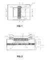
- FIG. 1is a plan view showing a main part of a semiconductor device according to a first embodiment of the present invention
- FIG. 2is a sectional view of the semiconductor device taken along the line A-A′ of FIG. 1 according to the first embodiment of the present invention
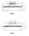
- FIG. 3is a sectional view of the semiconductor device taken along the line B-B′ of FIG. 1 according to the first embodiment of the present invention
- FIG. 4is a sectional view of the semiconductor device taken along the line C-C′ of FIG. 1 according to the first embodiment of the present invention
- FIGS. 5A and 5Bare sectional views each showing the semiconductor device taken along the line A-A′ of FIG. 1 and further showing a manufacturing process thereof according to the first embodiment of the present invention
- FIGS. 6A and 6Bare sectional views each showing the semiconductor device taken along the line A-A′ of FIG. 1 and further showing the manufacturing process thereof according to the first embodiment of the present invention
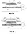
- FIGS. 7A and 7Bare sectional views each showing the semiconductor device taken along the line A-A′ of FIG. 1 and further showing the manufacturing process thereof according to the first embodiment of the present invention
- FIGS. 8A and 8Bare sectional views each showing a semiconductor device taken along the line B-B′ of FIG. 1 and further showing a manufacturing process thereof according to the first embodiment of the present invention
- FIGS. 9A and 9Bare sectional views each showing the semiconductor device taken along the line B-B′ of FIG. 1 and further showing the manufacturing process thereof according to the first embodiment of the present invention
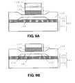
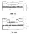
- FIGS. 10A and 10Bare sectional views each showing a semiconductor device taken along the line C-C′ of FIG. 1 and further showing a manufacturing process thereof according to the first embodiment of the present invention
- FIGS. 11A and 11Bare sectional views each showing the semiconductor device taken along the line C-C′ of FIG. 1 and further showing the manufacturing process thereof according to the first embodiment of the present invention.
- FIG. 12Ais a plan view of an n-type MOS transistor having a body contact region formed therein according to another embodiment of the present invention
- FIG. 12Bis a sectional view of the n-type MOS transistor taken along the line D-D′ of FIG. 12A .
- FIGS. 1 to 4are plan views and sectional views each showing a main part of a semiconductor device according to an embodiment of the present invention.
- FIG. 2is a sectional view of the semiconductor device taken along the line A-A′ of FIG. 1 .
- FIG. 3is a sectional view of the semiconductor device taken along the line B-B′ of FIG. 1 .
- FIG. 4is a sectional view of the semiconductor device taken along the line C-C′ of FIG. 1 .
- a semiconductor substrate 101is a p-type bonded silicon on insulator (SOI) substrate which has, for example, a three-layered structure of a p-type single crystal semiconductor substrate 102 , a buried insulating film 103 having a film thickness of about 50 to 400 nm, and a p-type silicon active layer 104 having a thickness of about 50 to 200 nm.
- SOIsilicon on insulator
- the buried insulating film 103insulates the single crystal semiconductor supporting substrate 102 and the p-type silicon active layer 104 from each other.
- Each concentration of the p-type single crystal semiconductor supporting substrate 102 and the p-type silicon active layer 104is generally in about a range from 1 ⁇ 10 14 cm ⁇ 3 to 1 ⁇ 10 15 cm ⁇ 3 .
- the p-type bonded substrateis used as the SOI substrate 101 .
- An n-type MOS transistoris formed on the silicon active layer 104 formed on the buried insulating layer 103 .
- the MOS transistoris electrically insulated from the periphery by a field insulating film 105 which is formed by a local oxidation of silicon (LOCOS) process with a thickness of about 100 to 500 nm and is in contact with the buried insulating film 103 .
- LOCOSlocal oxidation of silicon
- a gate electrode 111which is composed of an n-type impurity region 108 and p-type impurity regions 109 which are formed of polysilicon having a thickness of about 200 to 300 nm, and a refractory metal silicide 110 deposited on the polysilicon.
- the n-type impurity region 108 and the p-type impurity regions 109 of the gate electrodeare formed through ion implantation in the polysilicon by changing an ion species so that a channel region becomes an n-type region and the LOCOS isolation edge becomes a p-type region.
- a sheet resistance of the gate electrode 111is reduced.
- a source region 112 and a drain region 113are configured respectively.
- N-type conductive polysilicon in the channel region and p-type conductive polysilicon at the LOCOS isolation edgeenables to lower the threshold voltage in the channel region of the NMOS, and to increase the threshold voltage at the LOCOS isolation edge due to a difference between work functions of each of a p-type gate and a p-type silicon active layer. As a result, it is possible to suppress generation of the parasitic MOS transistor at the LOCOS isolation edge while driving the transistor at a low drive voltage in the channel region of the NMOS transistor.
- the SOI substrate 101 having the three-layered structure of the p-type single crystal semiconductor supporting substrate 102 , the buried insulating film 103 having the film thickness of about 50 to 400 nm, and the p-type silicon active layer 104 having the thickness about 50 to 200 nm as shown in FIG. 5Athe filed insulating film 106 having the film thickness of about 100 to 500 nm as shown in FIG. 5B is formed by the LOCOS process.
- a silicon oxide film having a film thickness of about 5 to 30 nmis formed as the gate insulating film 106 by thermal oxidation.
- the polysilicon layer 107 which serves as the gate electrode of the MOS transistoris deposited with a thickness of about 200 to 400 nm.
- the surface of the polysilicon layer 107is subjected to patterning with a photo resist 114 , and is partially implanted with an n-type impurity such as arsenic by ion implantation.
- the portionbecomes thereafter the n-type region 108 for the channel region of the gate electrode 111 .
- a dosage thereofis 5 ⁇ 1015 cm ⁇ 2.
- the patterningis performed with the photo resist 114 , and the ion implantation is partially performed with the p-type impurity such as BF2.
- the portionbecomes thereafter the p-type region 109 for the LOCOS isolation edge of the gate electrode 111 .
- the ion implantationis performed with a dosage thereof is about 8 ⁇ 10 15 cm ⁇ 2 .
- the semiconductor substrate 101is subjected to thermal treatment at a temperature of about 850° C. to diffuse the impurity provided in the gate electrode 111 .
- the refractory metal silicide 110is deposited with a thickness of about 100 nm, and is subjected to patterning of the photo resist and etching, to thereby form the gate electrode 111 having the n-type region 108 and the p-type regions 109 .
- the ion implantation methodis employed to form the n-type region 108 and the p-type regions 109 , but phosphorus pre-deposition may be employed to form the n-type region and boron pre-deposition may be employed to form the p-type region.
- the pre-depositionis performed after patterning is performed with an oxide film as a hard mask to form the gate electrode.
- the pre-depositionmay be employed to form the n-type region, and the ion implantation may be employed to form the p-type region.
- the pre-depositionmay be employed to form the p-type region, and the ion implantation may be employed to form the n-type region.
- the pre-depositionis performed first, the hard mask is removed, and then the ion implantation is performed on the entire surface, thereby making it possible to suppress, for example, penetration of the boron.
- FIGS. 8A , 8 B, 9 A, and 9 Bare sectional views each showing the semiconductor device taken along the line B-B′ of FIG. 1
- FIGS. 10A , 10 B, 11 A, and 11 Bare sectional views each showing the semiconductor device taken along the line C-C′ of FIG. 1 .
- Those figuresfurther show processes following the process shown in FIGS. 7A and 7B . As shown in FIGS.
- ion implantationis performed with a high concentration n-type impurity such as an arsenic with the formed gate electrode 111 and the filed insulating film 105 being used as masks, to thereby form the source region 112 and the drain region 113 .
- a concentration of the source and drain regionsis generally about 5 ⁇ 10 19 cm ⁇ 3 to 1 ⁇ 10 21 cm ⁇ 3 .
- an interlayer insulation film(not shown) is deposited thereon so as to electrically connect the source region 112 and the drain region 113 , and the gate electrode 111 to one another.
- FIG. 12shows a second embodiment of the present invention.
- FIG. 12Ais a plan view of an n-type MOS transistor using the SOI substrate 101
- FIG. 12Bis a sectional view of the n-type MOS transistor taken along the line D-D′ of FIG. 12A .
- the NMOS transistorhas a structure in which a p+ body contact region 115 is formed in the source region 112 .
- the polysilicon gate electrode 111has a structure in which the channel region becomes n-type and the LOCOS isolation edge regions become p-type in the same manner as in the first embodiment by impurity doping. As a result, it is possible to suppress generation of the parasitic MOS transistor at the LOCOS isolation edge. In addition, formation of the p+ body contact region 115 thereby enables to fix a potential of the substrate and suppress a substrate floating effect.
- n-type MOS transistoris described in this embodiment, but a p-type MOS transistor may be employed to obtain the similar structure.
Landscapes
- Engineering & Computer Science (AREA)
- Physics & Mathematics (AREA)
- Condensed Matter Physics & Semiconductors (AREA)
- General Physics & Mathematics (AREA)
- Manufacturing & Machinery (AREA)
- Computer Hardware Design (AREA)
- Microelectronics & Electronic Packaging (AREA)
- Power Engineering (AREA)
- Thin Film Transistor (AREA)
- Electrodes Of Semiconductors (AREA)
Abstract
Description
Claims (7)
Priority Applications (1)
| Application Number | Priority Date | Filing Date | Title |
|---|---|---|---|
| US12/901,055US8263443B2 (en) | 2006-02-07 | 2010-10-08 | Semiconductor device and method of manufacturing the same |
Applications Claiming Priority (8)
| Application Number | Priority Date | Filing Date | Title |
|---|---|---|---|
| JP2006029853 | 2006-02-07 | ||
| JPJP2006-029853 | 2006-02-07 | ||
| JP2006-029853 | 2006-02-07 | ||
| JP2007006234AJP5567247B2 (en) | 2006-02-07 | 2007-01-15 | Semiconductor device and manufacturing method thereof |
| JP2007-006234 | 2007-01-15 | ||
| JPJP2007-006234 | 2007-01-15 | ||
| US11/703,258US7851858B2 (en) | 2006-02-07 | 2007-02-07 | MOSFET having SOI and method |
| US12/901,055US8263443B2 (en) | 2006-02-07 | 2010-10-08 | Semiconductor device and method of manufacturing the same |
Related Parent Applications (1)
| Application Number | Title | Priority Date | Filing Date |
|---|---|---|---|
| US11/703,258DivisionUS7851858B2 (en) | 2006-02-07 | 2007-02-07 | MOSFET having SOI and method |
Publications (2)
| Publication Number | Publication Date |
|---|---|
| US20110027949A1 US20110027949A1 (en) | 2011-02-03 |
| US8263443B2true US8263443B2 (en) | 2012-09-11 |
Family
ID=38478072
Family Applications (2)
| Application Number | Title | Priority Date | Filing Date |
|---|---|---|---|
| US11/703,258Expired - Fee RelatedUS7851858B2 (en) | 2006-02-07 | 2007-02-07 | MOSFET having SOI and method |
| US12/901,055Expired - Fee RelatedUS8263443B2 (en) | 2006-02-07 | 2010-10-08 | Semiconductor device and method of manufacturing the same |
Family Applications Before (1)
| Application Number | Title | Priority Date | Filing Date |
|---|---|---|---|
| US11/703,258Expired - Fee RelatedUS7851858B2 (en) | 2006-02-07 | 2007-02-07 | MOSFET having SOI and method |
Country Status (5)
| Country | Link |
|---|---|
| US (2) | US7851858B2 (en) |
| JP (1) | JP5567247B2 (en) |
| KR (1) | KR101355282B1 (en) |
| CN (1) | CN101017851B (en) |
| TW (1) | TWI412130B (en) |
Cited By (1)
| Publication number | Priority date | Publication date | Assignee | Title |
|---|---|---|---|---|
| US9698167B2 (en) | 2014-07-15 | 2017-07-04 | Samsung Display Co., Ltd. | Film transistor array panel and manufacturing method thereof |
Families Citing this family (11)
| Publication number | Priority date | Publication date | Assignee | Title |
|---|---|---|---|---|
| JP4560100B2 (en)* | 2008-03-24 | 2010-10-13 | 株式会社東芝 | Semiconductor device |
| JP2012129348A (en)* | 2010-12-15 | 2012-07-05 | Sanken Electric Co Ltd | Semiconductor device and method of manufacturing semiconductor device |
| CN108022970A (en)* | 2016-11-03 | 2018-05-11 | 中芯国际集成电路制造(上海)有限公司 | Semiconductor devices and forming method thereof |
| US10115787B1 (en)* | 2017-06-07 | 2018-10-30 | Psemi Corporation | Low leakage FET |
| CN107452755B (en)* | 2017-07-27 | 2020-01-21 | 武汉天马微电子有限公司 | Array substrate, manufacturing method thereof and display panel |
| US10468410B2 (en)* | 2017-11-15 | 2019-11-05 | Taiwan Semiconductor Manufacturing Co., Ltd. | Metal gate modulation to improve kink effect |
| CN108447904B (en)* | 2018-03-14 | 2020-09-29 | 电子科技大学 | Manufacturing method of transverse IGBT |
| CN111092112B (en)* | 2018-10-23 | 2020-11-13 | 合肥晶合集成电路有限公司 | MOS field effect transistor and method of making the same |
| TWI670491B (en) | 2018-12-10 | 2019-09-01 | 財團法人工業技術研究院 | Electrochemical processing device and method for operating electrochemical processing device |
| US12089412B2 (en) | 2020-03-26 | 2024-09-10 | Intel NDTM US LLC | Vertical string driver with extended gate junction structure |
| US12148802B2 (en)* | 2020-03-26 | 2024-11-19 | Intel NDTM US LLC | Vertical string driver with channel field management structure |
Citations (19)
| Publication number | Priority date | Publication date | Assignee | Title |
|---|---|---|---|---|
| US4178674A (en)* | 1978-03-27 | 1979-12-18 | Intel Corporation | Process for forming a contact region between layers of polysilicon with an integral polysilicon resistor |
| US4282648A (en) | 1980-03-24 | 1981-08-11 | Intel Corporation | CMOS process |
| US4466174A (en) | 1981-12-28 | 1984-08-21 | Texas Instruments Incorporated | Method for fabricating MESFET device using a double LOCOS process |
| US4700461A (en) | 1986-09-29 | 1987-10-20 | Massachusetts Institute Of Technology | Process for making junction field-effect transistors |
| US4700454A (en) | 1985-11-04 | 1987-10-20 | Intel Corporation | Process for forming MOS transistor with buried oxide regions for insulation |
| JPH08181316A (en) | 1994-12-22 | 1996-07-12 | Mitsubishi Electric Corp | Semiconductor device and manufacturing method thereof |
| US5686347A (en)* | 1994-12-27 | 1997-11-11 | United Microelectronics Corporation | Self isolation manufacturing method |
| US5893729A (en) | 1995-06-28 | 1999-04-13 | Honeywell Inc. | Method of making SOI circuit for higher temperature and higher voltage applications |
| JP2000306994A (en) | 1999-04-26 | 2000-11-02 | Oki Electric Ind Co Ltd | Semiconductor device of soi structure and fabrication thereof |
| US6214657B1 (en) | 1997-07-31 | 2001-04-10 | Hyundai Electronics Industries Co., Ltd. | Semiconductor device isolation structure and fabrication method of semiconductor device using the same |
| JP2001148481A (en) | 1999-11-19 | 2001-05-29 | Sumitomo Metal Ind Ltd | Semiconductor device and method of manufacturing the same |
| US6303441B1 (en) | 1998-05-14 | 2001-10-16 | Hyundai Electronics Industries Co., Ltd. | Semiconductor device and method for fabricating the same |
| US20030068870A1 (en) | 2001-10-10 | 2003-04-10 | Hirotaka Komatsubara | Method of manufacturing semiconductor element |
| US6768174B2 (en) | 2001-09-07 | 2004-07-27 | Seiko Instruments Inc. | Complementary MOS transistors having p-type gate electrodes |
| US6849887B2 (en)* | 1997-06-24 | 2005-02-01 | Matsushita Electric Industrial Co., Ltd. | Semiconductor device and method for fabricating the same |
| US6911694B2 (en)* | 2001-06-27 | 2005-06-28 | Ricoh Company, Ltd. | Semiconductor device and method for fabricating such device |
| US6987065B2 (en) | 2003-01-10 | 2006-01-17 | Matsushita Electric Industrial Co., Ltd. | Method of manufacturing self aligned electrode with field insulation |
| US7473947B2 (en) | 2002-07-12 | 2009-01-06 | Intel Corporation | Process for ultra-thin body SOI devices that incorporate EPI silicon tips and article made thereby |
| US20110108919A1 (en)* | 2006-02-22 | 2011-05-12 | International Business Machines Corporation | Method of fabricating a precision buried resistor |
Family Cites Families (9)
| Publication number | Priority date | Publication date | Assignee | Title |
|---|---|---|---|---|
| JPS59134878A (en)* | 1983-01-21 | 1984-08-02 | Toshiba Corp | Semiconductor device |
| KR970052023A (en)* | 1995-12-30 | 1997-07-29 | 김주용 | S-O I device and its manufacturing method |
| JP3648015B2 (en)* | 1997-05-14 | 2005-05-18 | 株式会社ルネサステクノロジ | Semiconductor device |
| JP2002270614A (en)* | 2001-03-12 | 2002-09-20 | Canon Inc | SOI substrate, heat treatment method thereof, semiconductor device having the same, and method of manufacturing the same |
| JP4044446B2 (en)* | 2002-02-19 | 2008-02-06 | セイコーインスツル株式会社 | Semiconductor device and manufacturing method thereof |
| JP4083507B2 (en)* | 2002-08-28 | 2008-04-30 | セイコーインスツル株式会社 | Manufacturing method of semiconductor device |
| KR101025917B1 (en)* | 2003-06-26 | 2011-03-30 | 매그나칩 반도체 유한회사 | MOOS transistor and its manufacturing method |
| JP4700268B2 (en)* | 2003-09-19 | 2011-06-15 | セイコーエプソン株式会社 | Semiconductor device and manufacturing method of semiconductor device |
| JP2007123519A (en)* | 2005-10-27 | 2007-05-17 | Seiko Epson Corp | Semiconductor device manufacturing method and semiconductor device |
- 2007
- 2007-01-15JPJP2007006234Apatent/JP5567247B2/ennot_activeExpired - Fee Related
- 2007-02-05TWTW096104125Apatent/TWI412130B/ennot_activeIP Right Cessation
- 2007-02-07CNCN2007100879502Apatent/CN101017851B/ennot_activeExpired - Fee Related
- 2007-02-07USUS11/703,258patent/US7851858B2/ennot_activeExpired - Fee Related
- 2007-02-07KRKR1020070012669Apatent/KR101355282B1/ennot_activeExpired - Fee Related
- 2010
- 2010-10-08USUS12/901,055patent/US8263443B2/ennot_activeExpired - Fee Related
Patent Citations (21)
| Publication number | Priority date | Publication date | Assignee | Title |
|---|---|---|---|---|
| US4178674A (en)* | 1978-03-27 | 1979-12-18 | Intel Corporation | Process for forming a contact region between layers of polysilicon with an integral polysilicon resistor |
| US4282648A (en) | 1980-03-24 | 1981-08-11 | Intel Corporation | CMOS process |
| US4466174A (en) | 1981-12-28 | 1984-08-21 | Texas Instruments Incorporated | Method for fabricating MESFET device using a double LOCOS process |
| US4700454A (en) | 1985-11-04 | 1987-10-20 | Intel Corporation | Process for forming MOS transistor with buried oxide regions for insulation |
| US4700461A (en) | 1986-09-29 | 1987-10-20 | Massachusetts Institute Of Technology | Process for making junction field-effect transistors |
| JPH08181316A (en) | 1994-12-22 | 1996-07-12 | Mitsubishi Electric Corp | Semiconductor device and manufacturing method thereof |
| US5686347A (en)* | 1994-12-27 | 1997-11-11 | United Microelectronics Corporation | Self isolation manufacturing method |
| US5893729A (en) | 1995-06-28 | 1999-04-13 | Honeywell Inc. | Method of making SOI circuit for higher temperature and higher voltage applications |
| US6849887B2 (en)* | 1997-06-24 | 2005-02-01 | Matsushita Electric Industrial Co., Ltd. | Semiconductor device and method for fabricating the same |
| US6214657B1 (en) | 1997-07-31 | 2001-04-10 | Hyundai Electronics Industries Co., Ltd. | Semiconductor device isolation structure and fabrication method of semiconductor device using the same |
| US6303441B1 (en) | 1998-05-14 | 2001-10-16 | Hyundai Electronics Industries Co., Ltd. | Semiconductor device and method for fabricating the same |
| JP2000306994A (en) | 1999-04-26 | 2000-11-02 | Oki Electric Ind Co Ltd | Semiconductor device of soi structure and fabrication thereof |
| JP2001148481A (en) | 1999-11-19 | 2001-05-29 | Sumitomo Metal Ind Ltd | Semiconductor device and method of manufacturing the same |
| US6911694B2 (en)* | 2001-06-27 | 2005-06-28 | Ricoh Company, Ltd. | Semiconductor device and method for fabricating such device |
| US6768174B2 (en) | 2001-09-07 | 2004-07-27 | Seiko Instruments Inc. | Complementary MOS transistors having p-type gate electrodes |
| US20030068870A1 (en) | 2001-10-10 | 2003-04-10 | Hirotaka Komatsubara | Method of manufacturing semiconductor element |
| US6673660B2 (en) | 2001-10-10 | 2004-01-06 | Oki Electric Industry Co, Ltd. | Method of manufacturing semiconductor element |
| US7473947B2 (en) | 2002-07-12 | 2009-01-06 | Intel Corporation | Process for ultra-thin body SOI devices that incorporate EPI silicon tips and article made thereby |
| US6987065B2 (en) | 2003-01-10 | 2006-01-17 | Matsushita Electric Industrial Co., Ltd. | Method of manufacturing self aligned electrode with field insulation |
| US7235830B2 (en) | 2003-01-10 | 2007-06-26 | Matsushita Electric Industrial Co., Ltd. | Semiconductor device and process for manufacturing the same |
| US20110108919A1 (en)* | 2006-02-22 | 2011-05-12 | International Business Machines Corporation | Method of fabricating a precision buried resistor |
Cited By (1)
| Publication number | Priority date | Publication date | Assignee | Title |
|---|---|---|---|---|
| US9698167B2 (en) | 2014-07-15 | 2017-07-04 | Samsung Display Co., Ltd. | Film transistor array panel and manufacturing method thereof |
Also Published As
| Publication number | Publication date |
|---|---|
| JP2007243156A (en) | 2007-09-20 |
| TW200805654A (en) | 2008-01-16 |
| US7851858B2 (en) | 2010-12-14 |
| CN101017851B (en) | 2010-06-23 |
| KR20070080583A (en) | 2007-08-10 |
| TWI412130B (en) | 2013-10-11 |
| KR101355282B1 (en) | 2014-01-27 |
| US20070210382A1 (en) | 2007-09-13 |
| US20110027949A1 (en) | 2011-02-03 |
| JP5567247B2 (en) | 2014-08-06 |
| CN101017851A (en) | 2007-08-15 |
Similar Documents
| Publication | Publication Date | Title |
|---|---|---|
| US8263443B2 (en) | Semiconductor device and method of manufacturing the same | |
| JP2940880B2 (en) | Semiconductor device and manufacturing method thereof | |
| JP3337953B2 (en) | SOI MOSFET and manufacturing method thereof | |
| JP2707977B2 (en) | MOS type semiconductor device and method of manufacturing the same | |
| US6825528B2 (en) | Semiconductor device, method of manufacture thereof, and information processing device | |
| JP2701762B2 (en) | Semiconductor device and manufacturing method thereof | |
| US6352872B1 (en) | SOI device with double gate and method for fabricating the same | |
| JP2001156290A (en) | Semiconductor device | |
| US6995055B2 (en) | Structure of a semiconductor integrated circuit and method of manufacturing the same | |
| US6172405B1 (en) | Semiconductor device and production process therefore | |
| JP2007005575A (en) | Semiconductor device and manufacturing method thereof | |
| JP2000332250A (en) | Semiconductor device and manufacturing method thereof | |
| US20040169224A1 (en) | Semiconductor device and manufacturing method therefor | |
| JPH07211902A (en) | Mis type transistor and its manufacture | |
| JPH1154758A (en) | Semiconductor integrated circuit device and method of manufacturing the same | |
| JP2729422B2 (en) | Semiconductor device | |
| JPH11354785A (en) | Field effect transistor, semiconductor integrated circuit device having the same, and method of manufacturing the same | |
| JPH09135029A (en) | MIS type semiconductor device and manufacturing method thereof | |
| JP2006186180A (en) | Semiconductor device and manufacturing method thereof | |
| JP2796655B2 (en) | Semiconductor device and manufacturing method thereof | |
| JPH0851198A (en) | Semiconductor device | |
| KR100305625B1 (en) | Semiconductor device and method of manufacturing the same | |
| JP2013258432A (en) | Semiconductor device, and method for manufacturing the same | |
| JP2004207528A (en) | Semiconductor device and manufacturing method thereof | |
| JP2004207529A (en) | Semiconductor device and manufacturing method thereof |
Legal Events
| Date | Code | Title | Description |
|---|---|---|---|
| ZAAA | Notice of allowance and fees due | Free format text:ORIGINAL CODE: NOA | |
| ZAAB | Notice of allowance mailed | Free format text:ORIGINAL CODE: MN/=. | |
| STCF | Information on status: patent grant | Free format text:PATENTED CASE | |
| FEPP | Fee payment procedure | Free format text:PAYOR NUMBER ASSIGNED (ORIGINAL EVENT CODE: ASPN); ENTITY STATUS OF PATENT OWNER: LARGE ENTITY | |
| AS | Assignment | Owner name:SII SEMICONDUCTOR CORPORATION ., JAPAN Free format text:ASSIGNMENT OF ASSIGNORS INTEREST;ASSIGNOR:SEIKO INSTRUMENTS INC;REEL/FRAME:037783/0166 Effective date:20160209 | |
| AS | Assignment | Owner name:SII SEMICONDUCTOR CORPORATION, JAPAN Free format text:CORRECTIVE ASSIGNMENT TO CORRECT THE EXECUTION DATE PREVIOUSLY RECORDED AT REEL: 037783 FRAME: 0166. ASSIGNOR(S) HEREBY CONFIRMS THE ASSIGNMENT;ASSIGNOR:SEIKO INSTRUMENTS INC;REEL/FRAME:037903/0928 Effective date:20160201 | |
| FPAY | Fee payment | Year of fee payment:4 | |
| AS | Assignment | Owner name:ABLIC INC., JAPAN Free format text:CHANGE OF NAME;ASSIGNOR:SII SEMICONDUCTOR CORPORATION;REEL/FRAME:045567/0927 Effective date:20180105 | |
| MAFP | Maintenance fee payment | Free format text:PAYMENT OF MAINTENANCE FEE, 8TH YEAR, LARGE ENTITY (ORIGINAL EVENT CODE: M1552); ENTITY STATUS OF PATENT OWNER: LARGE ENTITY Year of fee payment:8 | |
| AS | Assignment | Owner name:ABLIC INC., JAPAN Free format text:CHANGE OF ADDRESS;ASSIGNOR:ABLIC INC.;REEL/FRAME:064021/0575 Effective date:20230424 | |
| FEPP | Fee payment procedure | Free format text:MAINTENANCE FEE REMINDER MAILED (ORIGINAL EVENT CODE: REM.); ENTITY STATUS OF PATENT OWNER: LARGE ENTITY | |
| LAPS | Lapse for failure to pay maintenance fees | Free format text:PATENT EXPIRED FOR FAILURE TO PAY MAINTENANCE FEES (ORIGINAL EVENT CODE: EXP.); ENTITY STATUS OF PATENT OWNER: LARGE ENTITY | |
| STCH | Information on status: patent discontinuation | Free format text:PATENT EXPIRED DUE TO NONPAYMENT OF MAINTENANCE FEES UNDER 37 CFR 1.362 | |
| FP | Lapsed due to failure to pay maintenance fee | Effective date:20240911 |