US8260378B2 - Mobile phone - Google Patents
Mobile phoneDownload PDFInfo
- Publication number
- US8260378B2 US8260378B2US12/583,158US58315809AUS8260378B2US 8260378 B2US8260378 B2US 8260378B2US 58315809 AUS58315809 AUS 58315809AUS 8260378 B2US8260378 B2US 8260378B2
- Authority
- US
- United States
- Prior art keywords
- carbon nanotube
- nanotube film
- mobile phone
- touch panel
- conductive layer
- Prior art date
- Legal status (The legal status is an assumption and is not a legal conclusion. Google has not performed a legal analysis and makes no representation as to the accuracy of the status listed.)
- Active, expires
Links
- 239000002238carbon nanotube filmSubstances0.000claimsabstractdescription119
- OKTJSMMVPCPJKN-UHFFFAOYSA-NCarbonChemical compound[C]OKTJSMMVPCPJKN-UHFFFAOYSA-N0.000claimsabstractdescription81
- 239000002041carbon nanotubeSubstances0.000claimsabstractdescription80
- 229910021393carbon nanotubeInorganic materials0.000claimsabstractdescription80
- 239000010410layerSubstances0.000claimsdescription95
- 239000000758substrateSubstances0.000claimsdescription33
- 238000002161passivationMethods0.000claimsdescription7
- 125000006850spacer groupChemical group0.000claimsdescription5
- 239000002048multi walled nanotubeSubstances0.000claimsdescription3
- 239000002079double walled nanotubeSubstances0.000claimsdescription2
- VNWKTOKETHGBQD-UHFFFAOYSA-NmethaneChemical compoundCVNWKTOKETHGBQD-UHFFFAOYSA-N0.000claimsdescription2
- 239000011241protective layerSubstances0.000claimsdescription2
- 239000002109single walled nanotubeSubstances0.000claimsdescription2
- 238000005411Van der Waals forceMethods0.000claims1
- 239000010408filmSubstances0.000description26
- 230000001681protective effectEffects0.000description13
- 230000006870functionEffects0.000description7
- 239000000463materialSubstances0.000description7
- 238000000034methodMethods0.000description6
- 229920005989resinPolymers0.000description6
- 239000011347resinSubstances0.000description6
- VYPSYNLAJGMNEJ-UHFFFAOYSA-Nsilicon dioxideInorganic materialsO=[Si]=OVYPSYNLAJGMNEJ-UHFFFAOYSA-N0.000description6
- 239000005020polyethylene terephthalateSubstances0.000description5
- 229920000139polyethylene terephthalatePolymers0.000description5
- -1polyethylene terephthalatePolymers0.000description4
- UMVBXBACMIOFDO-UHFFFAOYSA-N[N].[Si]Chemical compound[N].[Si]UMVBXBACMIOFDO-UHFFFAOYSA-N0.000description3
- 239000011521glassSubstances0.000description3
- 239000004033plasticSubstances0.000description3
- 229920003023plasticPolymers0.000description3
- 229920003229poly(methyl methacrylate)Polymers0.000description3
- 239000004926polymethyl methacrylateSubstances0.000description3
- 238000003825pressingMethods0.000description3
- 229910052814silicon oxideInorganic materials0.000description3
- 230000005236sound signalEffects0.000description3
- UMIVXZPTRXBADB-UHFFFAOYSA-NbenzocyclobuteneChemical classC1=CC=C2CCC2=C1UMIVXZPTRXBADB-UHFFFAOYSA-N0.000description2
- 230000003247decreasing effectEffects0.000description2
- 239000010432diamondSubstances0.000description2
- 229910003460diamondInorganic materials0.000description2
- 238000006056electrooxidation reactionMethods0.000description2
- 230000004313glareEffects0.000description2
- AMGQUBHHOARCQH-UHFFFAOYSA-Nindium;oxotinChemical compound[In].[Sn]=OAMGQUBHHOARCQH-UHFFFAOYSA-N0.000description2
- 239000004973liquid crystal related substanceSubstances0.000description2
- 229910052751metalInorganic materials0.000description2
- 239000002184metalSubstances0.000description2
- 229920002492poly(sulfone)Polymers0.000description2
- 230000035945sensitivityEffects0.000description2
- 235000012239silicon dioxideNutrition0.000description2
- 229920000178Acrylic resinPolymers0.000description1
- 239000004925Acrylic resinSubstances0.000description1
- RYGMFSIKBFXOCR-UHFFFAOYSA-NCopperChemical compound[Cu]RYGMFSIKBFXOCR-UHFFFAOYSA-N0.000description1
- 239000004721Polyphenylene oxideSubstances0.000description1
- 238000007550Rockwell hardness testMethods0.000description1
- NIXOWILDQLNWCW-UHFFFAOYSA-Nacrylic acid groupChemical groupC(C=C)(=O)ONIXOWILDQLNWCW-UHFFFAOYSA-N0.000description1
- 229910052787antimonyInorganic materials0.000description1
- WATWJIUSRGPENY-UHFFFAOYSA-Nantimony atomChemical compound[Sb]WATWJIUSRGPENY-UHFFFAOYSA-N0.000description1
- 229910052802copperInorganic materials0.000description1
- 239000010949copperSubstances0.000description1
- 238000010586diagramMethods0.000description1
- 239000011888foilSubstances0.000description1
- 238000001659ion-beam spectroscopyMethods0.000description1
- 238000001000micrographMethods0.000description1
- 239000003960organic solventSubstances0.000description1
- 239000004417polycarbonateSubstances0.000description1
- 229920000515polycarbonatePolymers0.000description1
- 229920000728polyesterPolymers0.000description1
- 229920000570polyetherPolymers0.000description1
- 229920000642polymerPolymers0.000description1
- 239000002952polymeric resinSubstances0.000description1
- 230000001737promoting effectEffects0.000description1
- 239000010453quartzSubstances0.000description1
- 239000010703siliconSubstances0.000description1
- 229910052710siliconInorganic materials0.000description1
- 239000000377silicon dioxideSubstances0.000description1
- 229910052709silverInorganic materials0.000description1
- 239000004332silverSubstances0.000description1
- 239000000126substanceSubstances0.000description1
- 229920003002synthetic resinPolymers0.000description1
- 239000010409thin filmSubstances0.000description1
- XOLBLPGZBRYERU-UHFFFAOYSA-Ntin dioxideChemical compoundO=[Sn]=OXOLBLPGZBRYERU-UHFFFAOYSA-N0.000description1
- 229910001887tin oxideInorganic materials0.000description1
- 229920002554vinyl polymerPolymers0.000description1
Images


Classifications
- H—ELECTRICITY
- H04—ELECTRIC COMMUNICATION TECHNIQUE
- H04M—TELEPHONIC COMMUNICATION
- H04M1/00—Substation equipment, e.g. for use by subscribers
- H04M1/02—Constructional features of telephone sets
- H04M1/0202—Portable telephone sets, e.g. cordless phones, mobile phones or bar type handsets
- H04M1/026—Details of the structure or mounting of specific components
- H04M1/0266—Details of the structure or mounting of specific components for a display module assembly
- H—ELECTRICITY
- H04—ELECTRIC COMMUNICATION TECHNIQUE
- H04M—TELEPHONIC COMMUNICATION
- H04M2250/00—Details of telephonic subscriber devices
- H04M2250/22—Details of telephonic subscriber devices including a touch pad, a touch sensor or a touch detector
Definitions
- the present disclosurerelates to mobile phones, and, in particular, to a mobile phone employed with a touch panel based on carbon nanotubes.
- mobile phonesinclude a body, a display panel disposed on a surface of the body, and an input device, such as a keyboard mounted on the surface of the body.
- an input devicesuch as a keyboard mounted on the surface of the body.
- a resistance-typea capacitance-type
- an infrared-typea capacitance-type
- a surface sound wave-typea capacitance-type
- the resistance-type and capacitance-type touch panelshave been widely used in mobile phones because of higher accuracy and resolution.
- a typical capacitance-type touch panelincludes a glass substrate, a transparent conductive layer, and four electrodes. It is well known that a layer of an indium tin oxide (ITO) is adopted to function as the transparent conductive layer.
- ITOindium tin oxide
- the ITO layer of the touch panelhas poor mechanical durability, low chemical endurance, and uneven resistance over the entire area of the touch panel.
- the ITO layerhas relatively low transparency in humid environments. All the above-mentioned problems of the ITO layer tend to yield a touch panel with relatively low sensitivity, accuracy, and brightness.
- the ITO layeris generally formed by means of ion-beam sputtering, a relatively complicated method.
- FIG. 1is a schematic, partially exploded view of a first embodiment of a mobile phone having one embodiment of a resistive touch panel;
- FIG. 2is a block diagram of the mobile phone of FIG. 1 ;
- FIG. 3is an isometric, partially exploded view of the resistive touch panel of FIG. 1 ;
- FIG. 4is a schematic, cross-sectional view of the resistive touch panel of FIG. 1 ;
- FIG. 5is a scanning electron microscope image of the orderly carbon nanotube films used in the resistive touch panel of FIG. 1 ;
- FIG. 6is a schematic view of the resistive touch panel of FIG. 1 when in use
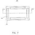
- FIG. 7is a top-view of one embodiment of a capacitive touch panel of a second embodiment of a mobile phone
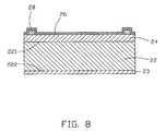
- FIG. 8is a schematic, cross-sectional view of the capacitive touch panel of FIG. 7 , taken alone line VII-VII;
- FIG. 9is a schematic, cross-sectional view of the capacitive touch panel of FIG. 7 when in use.
- first embodiment of a mobile phone 100includes a body 102 and a touch panel 10 .
- the body 102defines a display panel 104 .
- the touch panel 10is disposed on the display panel 104 .
- the body 102may further include a housing 190 , a communicating system, a central processing unit (CPU) 160 , a controlling unit 150 , and a memory unit 170 .
- the communicating systemincludes an antenna 192 , a microphone 194 , and a speaker 196 .
- the CPU 160 , the controlling unit 150 , the memory unit 170 , the microphone 194 , the speaker 196 , and the display panel 104are received in the housing 190 .
- the antenna 192may be received in the housing 190 or extend out of the surface of the housing 190 .
- the CPU 160 , the controlling unit 150 , and the memory unit 170may be mounted on an integrated circuit board.
- the memory unit 170 and the controlling unit 150are electrically connected to the CPU 160 via wires of the integrated circuit board.
- the speaker 196 , the microphone 194 , the antenna 192 , the display panel 104 , and the touch panel 10are electrically connected to the controlling unit 150 .
- the controlling unit 150includes a touch-panel controller, a display controller, and a communicating controller. These controllers are used for controlling the touch panel 10 , the display panel 104 , the speaker 196 , the microphone 194 , and the antenna 192 .
- the memory unit 170includes a random access memory and a read only memory and is configured to store instructions that can be dealt with and executed by the CPU 160 , and signals which are displayed via the display panel 104 .
- the antenna 192receives and sends radio frequency signals.
- the radio frequency signalsare transported to a processor and transformed into audio signals. Accordingly, the speaker 196 works under the control of the controlling unit 150 .
- the microphone 194receives sounds and transforms the sounds into audio signals. Then, the audio signals are transported to the CPU 160 and transformed into radio frequency signals and sent out via the antenna 192 under the control of the controlling unit 150 .
- the display panel 104may be a liquid crystal display panel, a field emission display panel, a plasma display panel, an electroluminescent display panel, or a vacuum fluorescent display panel.
- the display panel 104is used for displaying dates or views from the body 102 .
- the display panel 104is a liquid crystal display panel.
- the touch panel 10may be spaced apart from the display panel 104 or integrated with the display panel 104 .
- the touch panel 10When the touch panel 10 is integrated with the display panel 104 , it may be directly adhered onto a surface of the display panel 104 via paste or share a common substrate with the display panel 104 (that is to say, the second substrate 140 of the touch panel 10 functions as an emission plate of the display panel 104 ).
- Userscan input instructions for the body 102 via touching or pressing the touch panel 10 by using an input device, such as keyboard, pen, or finger.
- the touch panel 10is a resistive touch panel and includes a first electrode plate 12 , a second electrode plate 14 , and a plurality of transparent dot spacers 16 .
- the second electrode plate 14is directly adhered to the display panel 104 .
- the first electrode plate 12includes a first substrate 120 , a first conductive layer 122 , and two first electrodes 124 .
- the first substrate 120has a planar structure, and includes a first surface.
- the first conductive layer 122 and the two first electrodes 124are mounted on the first surface of the first substrate 120 .
- the two first electrodes 124are respectively disposed on the two ends of the first substrate 120 along a first direction and electrically connected to the first conductive layer 122 .
- the first directionis marked as the X-direction.
- the second electrode plate 14includes a second substrate 140 , a second conductive layer 142 and two electrodes 144 .
- the second substrate 140has a planar structure, and includes a second surface.
- the second surface of the second substrate 140is faced to the first surface of the first substrate 120 .
- the second conductive layer 142 and the two electrodes 144are disposed on the second surface of the second substrate 140 .
- the two electrodes 144are respectively disposed on the two ends of the second ends of the second substrate 140 along a second direction and electrically connected to the second conductive layer 142 .
- the second directionis marked as the Y direction.
- the X directionis substantially perpendicular to the Y direction, namely, the two first electrodes 124 are substantially orthogonal to the two second electrodes 144 .
- the first substrate 120can be a transparent and flexible film or plate made of polymer, resin, or any other suitable flexible material.
- the second substrate 140can be a rigid and transparent board made of glass, diamond, quartz, plastic or any other suitable material, or can be a transparent flexible film or plate similar to the first substrate 120 , if the touch panel 10 is flexible.
- a material of the flexible film or platecan be one or more of polycarbonate (PC), polymethyl methacrylate acrylic (PMMA), polyethylene terephthalate (PET), polyether polysulfones (PES), polyvinyl polychloride (PVC), benzocyclobutenes (BCB), polyesters, and acrylic resins.
- the thickness of the first substrate 120 and the second substrate 140can be in the range from about 5 millimeters to about 1 centimeter.
- an insulating pad 18is disposed on the periphery of the second surface of the second electrode plate 14 .
- the first electrode plate 12is disposed on the insulating pad 18 .
- the first conductive layer 122 of the first electrode plate 12is faced to the second conductive layer 142 of the second electrode plate 14 .
- the plurality of transparent dot spacer 16are spaced apart from one another and disposed on the second conductive layer 142 of the second electrode plate 14 .
- a distance between the first and second electrode plates 12 , 14is in a range of about 2 mm to about 100 mm.
- the insulating pad 18 and the dot spacers 16are made of transparent resin or the like and are used for insulating the first electrode plate 12 with the second electrode plate 14 . Understandably, if the resistive touch panel 10 is small enough, the dot spacers 16 may be omitted.
- a transparent protective film 126may be disposed on the top surface of the first electrode plate 12 .
- the transparent protective film 126may be directly adhered on the first electrode plate 12 via paste, or combined with the first electrode plate 12 via a heat-press method.
- the transparent protective film 126may be a plastic layer or a resin layer, which are treated via surface rigid treating.
- the resin layermay be made of benzo cyclo butene, polymethyl methacrylate, polymer resin, polyethylene terephthalate, or the like.
- the transparent protective film 126is made of polyethylene terephthalate, and configured for protecting the first electrode plate 12 by improving wearability thereof.
- the transparent protective film 126may provide some additional function, such as decreasing glare and reflection.
- At least one of the first and second conductive layers 122 , 142includes a carbon nanotube layer.
- the carbon nanotube layerincludes one or more carbon nanotube films.
- the carbon nanotube filmis formed by a plurality of carbon nanotubes, ordered or otherwise, and has a uniform thickness.
- the carbon nanotube filmcan be an ordered film or a disordered film.
- the ordered carbon nanotube filmconsists of ordered carbon nanotubes.
- Ordered carbon nanotube filmsinclude films where the carbon nanotubes are arranged along a primary direction. Examples include films where the carbon nanotubes are arranged approximately along a same direction or have two or more sections within each of which the carbon nanotubes are arranged approximately along a same direction (different sections can have different directions).
- the carbon nanotubescan be primarily oriented along a same direction.
- the ordered carbon nanotube filmcan also have sections of carbon nanotubes aligned in a common direction.
- the ordered carbon nanotube filmcan have two or more sections, and the sections can have different alignments.
- the ordered carbon nanotube filmmay have a free-standing structure.
- the free-standing carbon nanotube filmmay include two types. One type is that the carbon nanotube film needs no substrate to support the carbon nanotubes thereof. Another type is that the carbon nanotube film only needs one or more supporting dots (not shown) to support one or more points thereof. Thus, left parts of the carbon nanotube film are hung.
- the carbon nanotubesare oriented along a same preferred orientation and approximately parallel to each other.
- the term “approximately” as used hereinmeans that it is impossible and unnecessary that each of carbon nanotubes in the carbon nanotube films be exactly parallel to one another, namely that every carbon nanotubes is parallel to each other, because in the course of fabricating the carbon nanotube film, some factor, such as the change of drawing speed, affects the non-uniform drawing force on the carbon nanotube film as the carbon nanotube film is drawn from a carbon nanotube array.
- a filmcan be drawn from a carbon nanotube array, to form the ordered carbon nanotube film, namely a drawn carbon nanotube film.
- drawn carbon nanotube filmexamples include US 20080170982 to Zhang et al.
- the drawn carbon nanotube filmincludes a plurality of successive and oriented carbon nanotubes joined end-to-end by van der Waals attractive force therebetween.
- the drawn carbon nanotube filmis a free-standing film.
- the carbon nanotube filmcan be treated with an organic solvent to increase the mechanical strength and toughness of the carbon nanotube film and reduce the coefficient of friction of the carbon nanotube film.
- a thickness of the carbon nanotube filmcan range from about 0.5 nanometers to about 100 micrometers.
- the disordered carbon nanotube filmconsists of disordered carbon nanotubes.
- Disordered carbon nanotube filmsinclude randomly aligned carbon nanotubes. When the disordered carbon nanotube film has a number of the carbon nanotubes aligned in every direction that are substantially equal, the disordered carbon nanotube film can be isotropic. The disordered carbon nanotubes can be entangled with each other and/or are approximately parallel to a surface of the disordered carbon nanotube film.
- the disordered carbon nanotube filmmay be a flocculated carbon nanotube film.
- the flocculated carbon nanotube filmcan include a plurality of long, curved, disordered carbon nanotubes entangled with each other.
- the carbon nanotubes in the flocculated carbon nanotube filmcan be isotropic.
- the carbon nanotubescan be substantially uniformly dispersed in the carbon nanotube film. Adjacent carbon nanotubes are attracted by van der Waals attractive force to form an entangled structure with micropores defined therein. It is understood that the flocculated carbon nanotube film is very porous. Sizes of the micropores can be less than 10 micrometers. The porous nature of the flocculated carbon nanotube film will increase specific surface area of the carbon nanotube structure.
- the touch panel 10 employing the flocculated carbon nanotube filmhas excellent durability, and can be fashioned into desired shapes with a low risk to the integrity of the flocculated carbon nanotube film.
- the thickness of the flocculated carbon nanotube filmcan range from about 0.5 nanometers to about 1 millimeter.
- the pressed carbon nanotube filmcan be a free-standing carbon nanotube film.
- the carbon nanotubes in the pressed carbon nanotube filmmay be arranged along a same direction or arranged along different directions.
- the pressed carbon nanotube filmis a ordered carbon nanotube film.
- the pressed carbon nanotube filmis a disordered carbon nanotube film.
- the carbon nanotubes in the pressed carbon nanotube filmcan rest upon each other. Adjacent carbon nanotubes are attracted to each other and combined by van der Waals attractive force.
- An angle between a primary alignment direction of the carbon nanotubes and a surface of the pressed carbon nanotube filmis approximately 0 degrees to approximately 15 degrees. The greater the pressure applied, the smaller the angle formed.
- the pressed carbon nanotube filmcan be isotropic.
- the thickness of the pressed carbon nanotube filmranges from about 0.5 nm to about 1 mm. Examples of pressed carbon nanotube film are taught by US application 20080299031A1 to Liu et al.
- a length and a width of the carbon nanotube filmcan be arbitrarily set as desired.
- a thickness of the carbon nanotube filmis in a range from about 0.5 nanometers to about 100 micrometers.
- the carbon nanotubes in the carbon nanotube filmcan be selected from the group consisting of single-walled, double-walled, multi-walled carbon nanotubes, and combinations thereof. Diameters of the single-walled carbon nanotubes, the double-walled carbon nanotubes, and the multi-walled carbon nanotubes can, respectively, be in the approximate range from about 0.5 nanometers to about 50 nanometers, about 1 nanometer to about 50 nanometers, and about 1.5 nanometers to about 50 nanometers.
- the first conductive layer 122 and the second conductive layer 124each include a carbon nanotube layer.
- the carbon nanotube layeris an ordered carbon nanotube film.
- the carbon nanotube layermay include a number of carbon nanotube films stacked with each other.
- the carbon nanotubes of each of the carbon nanotube filmsare arranged alone a preferred orientation.
- the carbon nanotube filmincludes a number of carbon nanotube segments joined end by end via van der Waals attractive forces.
- the carbon nanotube segmentshave a substantially same length and composed of a number of approximately parallel arranged carbon nanotubes.
- the carbon nanotube films of the first conductive layer 122are overlapped alone the first direction, and the carbon nanotube films of the second conductive layer 124 are overlapped along the second direction.
- the carbon nanotube filmshave thickness of about 0.5 nm to 100 mm and width of 0.01 cm to about 10 cm.
- the mobile phone 100may further include a shielding layer 19 disposed on the bottom surface of the touch panel 10 .
- the material of the shielding layer 19can be a conductive resin film, a carbon nanotube film, or another kind of flexible and conductive film.
- the shielding layer 19is a carbon nanotube film.
- the carbon nanotube filmincludes a plurality of carbon nanotubes, and the orientation of the carbon nanotubes therein can be arbitrarily determined. Understandably, the carbon nanotubes in the carbon nanotube film of the shielding layer 19 can be arranged along a same direction.
- the carbon nanotube filmis connected to ground and acts as shielding, thus enabling the touch panel 10 to operate without interference (e.g., electromagnetic interference).
- the mobile phone 100may further include a passivation layer 13 interposed between the display panel 104 and the touch panel 10 .
- the passivation layer 13is used for preventing crosstalk, electrochemical corrosion, and so on, or reducing power consumption.
- the passivation layer 13may be made of silicon nitrogen, silicon oxide, or the like.
- a voltage of about 5 voltsis applied to the first and second electrodes 124 , 144 .
- Equipotential lines parallel to the first and second electrodesare formed in the first and second transparent conductive layers 122 , 142 .
- a useroperates the mobile phone 100 by pressing or touching the touch panel 10 with a touch tool 180 , such as a finger, or a pen/stylus, while visually observing the display panel 104 through the touch panel 10 .
- An input position 182can be determined from X-Y coordinates based on the X Y directions and corresponding to the potential of the input position 182 developed from the press or touch of the touch panel 10 .
- the controlling unit 150detects coordinates of the touch point on the touch panel 10 according to change of currents of the first and second electrodes 124 , 144 . Then the touch panel 10 sends the coordinates of the touch point to the CPU 160 .
- the CPU 160reads an instruction, according to the coordinates of the touch point, in the memory unit 170 , and sends the instruction to the controlling unit 150 .
- the controlling unit 150controls the display panel 104 , the antenna 192 , the microphone 194 , and the speaker 196 to operate according to the instruction.
- a second embodiment of a mobile phone 200includes a body (not shown) and a touch panel 20 .
- the bodydefines a display panel 204 thereon.
- the touch panel 20is disposed on the touch panel far away from the body.
- the touch panel 20is a capacitive touch panel.
- the touch panel 20includes a substrate 22 , a transparent conductive layer 24 , at least two electrodes 28 , and a transparent protective film 26 .
- the substrate 22is adjacent to the display panel 204 . It is appreciated that the substrate 22 may function as the top substrate of the display panel 204 , namely, the touch panel 20 shares a common substrate with the display panel 204 .
- the substrate 22includes a first surface 221 and a second surface 222 opposite to the first surface 221 .
- the first surface 221is far away from the display panel 204 .
- the transparent conductive layer 24is mounted on the first surface 221 of the substrate 22 .
- At least two electrodes 28are disposed at the periphery of the transparent conductive layer 24 , spaced from each other, and electrically connected to the transparent conductive layer 24 to form equipotential lines thereon.
- the transparent protective layer 26can be directly disposed on the transparent conductive layer 24 and the electrodes 28 .
- the touch panel 20has four electrodes 28 respectively disposed on the four sides of the transparent conductive layer 24 . Understandably, the four electrodes 28 can be disposed on the different surfaces of the transparent conductive layer 24 as long as equipotential lines can be formed on the transparent conductive layer 24 .
- the four electrodes 28can be disposed between the transparent conductive layer 24 and the substrate 22 and electrically connected to the transparent conductive layer 24 .
- the substrate 22has a curved structure or a planar structure and functions as a supporter for the touch panel 20 .
- the supporteris sandwiched between the touch panel 20 and the display panel 204 .
- the substrate 22is made of a rigid material or a flexible material, such as glass, silicon, diamond, plastic, or the like.
- the transparent conductive layer 24includes a carbon nanotube layer.
- the carbon nanotube layerincludes a number of uniformly arranged carbon nanotubes, and the carbon nanotubes are orderly, or disorderly arranged.
- the carbon nanotube layer of the transparent conductive layer 24has the same configuration as the first and second conductive layer 122 , 124 of the first embodiment of the mobile phone 100 .
- the four electrodes 28are made of metal, a carbon nanotube thin film, or the like.
- the four electrodes 28are layers of silver, copper, or foils of metal and have strip-shaped structures.
- a transparent protective film 26is disposed on the transparent conductive layer 24 and the electrodes 28 .
- the transparent protective film 26is made of polyethylene terephthalate, silicon nitrogen, silicon oxide or the like, and configured for protecting the transparent conductive layer 24 by improving wearability thereof.
- the transparent protective film 26may provide some additional function, such as decreasing glare and reflection after special treating.
- the transparent protective film 26which is made of silicon dioxide, is disposed on the transparent conductive layer 24 on which the electrodes 28 is mounted.
- the transparent protective film 26has a hardness of 7H (H established according to Rockwell hardness test). Understandably, the hardness and the thickness of the transparent protective film 26 may be varied in practice as desired.
- the transparent protective film 26is directly adhered on the transparent conductive layer 24 via paste.
- the mobile phone 200further includes a shielding layer 23 disposed on the second surface 222 of the touch panel 10 when the touch panel 20 is integrated with the display panel 204 .
- the material of the shielding layer 23can be a conductive resin film, indium tin oxide, antimony doped tin oxide, a carbon nanotube film, or another kind of flexible and conductive film.
- the shielding layer 23is a carbon nanotube film.
- the carbon nanotube filmincludes a plurality of carbon nanotubes, and the orientation of the carbon nanotubes therein can be arbitrarily determined. Understandably, the carbon nanotubes in the carbon nanotube film of the shielding layer can be arranged along a same direction.
- the carbon nanotube filmis connected to ground and acts as shielding, thus enabling the touch panel 20 to operate without interference (e.g., electromagnetic interference).
- the mobile phone 200further include a passivation layer 25 interposed between the display panel 204 and the touch panel 20 .
- the passivation layer 25is used for preventing crosstalk, electrochemical corrosion, and so on, or reducing power consumption.
- the passivation layer 25may be made of silicon nitrogen, silicon oxide, or the like.
- the capacitance at the touch pointchanges, which results in a change in frequency of an oscillator (not shown).
- a touch toolsuch as a finger, or a pen/stylus
- the coordinates of the input pointare detected.
- the controlling unit 250calculates the proportion of the four supplied currents of the four transparent electrodes 28 , thereby detecting coordinates of the touch point on the touch panel 20 .
- the controlling unit 250sends the coordinates of the touch point to the CPU 260 .
- the CPU 260reads an instruction according to the coordinates of the touch point in the memory unit 270 and sends the instruction to the controlling unit 250 .
- the controlling unit 250controls the display panel 204 , the antenna, the microphone, and the speaker to operate according to the instruction.
- the carbon nanotube films employed in the touch panelhas superior properties, such as excellent toughness, high mechanical strength, and uniform conductivity.
- the touch panel and the mobile phone using the sameare durable and highly conductive.
- Each of the carbon nanotube filmsincludes a number of successively oriented carbon nanotubes joined end to end by the van der Waals attractive force therebetween.
- the carbon nanotube filmsare flexible, and suitable for using as the conductive layer in a flexible touch panel.
- the carbon nanotube filmshave high transparency, thereby promoting improved brightness of the touch panel and the mobile phone using the same.
- the carbon nanotubeshave excellent electrical conductivity properties, the carbon nanotube films have a uniform resistance distribution.
- the touch panel and the mobile phone adopting the carbon nanotube filmshave improved sensitivity and accuracy.
Landscapes
- Engineering & Computer Science (AREA)
- Signal Processing (AREA)
- Position Input By Displaying (AREA)
- Telephone Set Structure (AREA)
Abstract
Description
Claims (20)
Applications Claiming Priority (3)
| Application Number | Priority Date | Filing Date | Title |
|---|---|---|---|
| CN200810142021 | 2008-08-22 | ||
| CN200810142021.1 | 2008-08-22 | ||
| CN200810142021ACN101656769B (en) | 2008-08-22 | 2008-08-22 | Mobile telephone |
Publications (2)
| Publication Number | Publication Date |
|---|---|
| US20100048254A1 US20100048254A1 (en) | 2010-02-25 |
| US8260378B2true US8260378B2 (en) | 2012-09-04 |
Family
ID=41696872
Family Applications (1)
| Application Number | Title | Priority Date | Filing Date |
|---|---|---|---|
| US12/583,158Active2030-11-10US8260378B2 (en) | 2008-08-22 | 2009-08-13 | Mobile phone |
Country Status (3)
| Country | Link |
|---|---|
| US (1) | US8260378B2 (en) |
| JP (1) | JP5237225B2 (en) |
| CN (1) | CN101656769B (en) |
Cited By (5)
| Publication number | Priority date | Publication date | Assignee | Title |
|---|---|---|---|---|
| US20100007619A1 (en)* | 2008-07-09 | 2010-01-14 | Tsinghua University | Touch panel, liquid crystal display screen using the same, and methods for making the touch panel and the liquid crystal display screen |
| US20140022497A1 (en)* | 2012-07-23 | 2014-01-23 | Tianjin Funayuanchuang Technology Co.,Ltd. | Liquid crystal display module |
| US20140022464A1 (en)* | 2012-07-23 | 2014-01-23 | Tianjin Funayuanchuang Technology Co.,Ltd. | Liquid crystal display module |
| US8982301B2 (en)* | 2012-07-23 | 2015-03-17 | Tianjin Funayuanchuang Technology Co., Ltd. | Method for making liquid crystal display module |
| US9557846B2 (en) | 2012-10-04 | 2017-01-31 | Corning Incorporated | Pressure-sensing touch system utilizing optical and capacitive systems |
Families Citing this family (14)
| Publication number | Priority date | Publication date | Assignee | Title |
|---|---|---|---|---|
| CN101620454A (en)* | 2008-07-04 | 2010-01-06 | 清华大学 | Potable computer |
| WO2009078283A1 (en)* | 2007-12-14 | 2009-06-25 | Ulvac, Inc. | Touch panel and method for manufacturing touch panel |
| TW201203041A (en) | 2010-03-05 | 2012-01-16 | Canatu Oy | A touch sensitive film and a touch sensing device |
| CN102262467A (en)* | 2010-05-28 | 2011-11-30 | 深圳富泰宏精密工业有限公司 | Touch transparent keyboard |
| CN201773379U (en)* | 2010-05-28 | 2011-03-23 | 深圳富泰宏精密工业有限公司 | Touch control type transparent keyboard |
| CN102262466A (en)* | 2010-05-28 | 2011-11-30 | 深圳富泰宏精密工业有限公司 | Touch transparent keyboard |
| CN102262446A (en)* | 2010-05-28 | 2011-11-30 | 深圳富泰宏精密工业有限公司 | Touch transparent keyboard |
| CN102262445A (en)* | 2010-05-28 | 2011-11-30 | 深圳富泰宏精密工业有限公司 | Touch transparent keyboard |
| CN101880035A (en) | 2010-06-29 | 2010-11-10 | 清华大学 | carbon nanotube structure |
| KR101167418B1 (en)* | 2010-09-20 | 2012-07-19 | 삼성전기주식회사 | Touch Screen |
| CN102289323A (en)* | 2011-08-31 | 2011-12-21 | 清华大学 | Display and display system |
| US9253892B2 (en)* | 2012-04-13 | 2016-02-02 | Wistron Corporation | Peripheral circuit of touch panel and manufacturing method thereof |
| US9351083B2 (en)* | 2013-10-17 | 2016-05-24 | Turtle Beach Corporation | Transparent parametric emitter |
| US9769573B2 (en)* | 2013-10-17 | 2017-09-19 | Turtle Beach Corporation | Transparent parametric transducer and related methods |
Citations (181)
| Publication number | Priority date | Publication date | Assignee | Title |
|---|---|---|---|---|
| JPS61231626A (en) | 1985-04-05 | 1986-10-15 | Asahi Chem Ind Co Ltd | Conductive sheet for position detection |
| JPS6263332U (en) | 1985-10-11 | 1987-04-20 | ||
| US4659873A (en) | 1985-07-19 | 1987-04-21 | Elographics, Inc. | Fabric touch sensor and method of manufacture |
| JPS62182916U (en) | 1986-05-08 | 1987-11-20 | ||
| JPS62190524U (en) | 1986-05-26 | 1987-12-04 | ||
| US4922061A (en) | 1988-06-13 | 1990-05-01 | Tektronix, Inc. | Capacitive touch panel system with randomly modulated position measurement signal |
| US4933660A (en) | 1989-10-27 | 1990-06-12 | Elographics, Inc. | Touch sensor with touch pressure capability |
| US5181030A (en) | 1989-12-28 | 1993-01-19 | Gunze Limited | Input system including resistance film touch panel and pushed position detecting device |
| JPH0628090Y2 (en) | 1992-06-03 | 1994-08-03 | 健一 古谷 | Electrode structure in used needle processing equipment |
| TW242732B (en) | 1993-06-29 | 1995-03-11 | Victor Company Of Japan | Digital chrominance signal processing circuit |
| TW284963B (en) | 1995-02-17 | 1996-09-01 | Nippon Tobacco Sangyo Kk | |
| TW284927B (en) | 1993-05-27 | 1996-09-01 | Mabuchi Motor Co | |
| JPH1063404A (en) | 1996-08-27 | 1998-03-06 | Matsushita Electric Ind Co Ltd | Coordinate position input device |
| TW341684B (en) | 1996-07-15 | 1998-10-01 | Synaptics Inc | Object position detector |
| US5853877A (en) | 1996-05-31 | 1998-12-29 | Hyperion Catalysis International, Inc. | Method for disentangling hollow carbon microfibers, electrically conductive transparent carbon microfibers aggregation film amd coating for forming such film |
| US5861583A (en) | 1992-06-08 | 1999-01-19 | Synaptics, Incorporated | Object position detector |
| JP2001267782A (en) | 2000-03-21 | 2001-09-28 | Shimadzu Corp | Electromagnetic wave absorption shielding material |
| US6373472B1 (en) | 1995-10-13 | 2002-04-16 | Silviu Palalau | Driver control interface system |
| US20020089492A1 (en) | 2001-01-11 | 2002-07-11 | Young-Soo Ahn | Flat panel display with input device |
| US6423583B1 (en) | 2001-01-03 | 2002-07-23 | International Business Machines Corporation | Methodology for electrically induced selective breakdown of nanotubes |
| TW498266B (en) | 2000-08-03 | 2002-08-11 | Hantouch Com | Resistive film type transparent analog touch panel |
| JP2002278701A (en) | 2001-03-21 | 2002-09-27 | Nissha Printing Co Ltd | Touch panel |
| WO2002076724A1 (en) | 2001-03-26 | 2002-10-03 | Eikos, Inc. | Coatings containing carbon nanotubes |
| TW508652B (en) | 2001-10-03 | 2002-11-01 | Taiwan Semiconductor Mfg | Device and method for wafer drying |
| TW521227B (en) | 2000-03-31 | 2003-02-21 | Sharp Kk | Electrode substrate, method for producing the same and display device including the same |
| CN2539375Y (en) | 2002-04-15 | 2003-03-05 | 湖南三才光电信息材料有限公司 | High-stable flexible transparent conducting composite film |
| US20030122800A1 (en) | 2001-12-27 | 2003-07-03 | Lg, Philips Lcd Co., Ltd. | Touch panel liquid crystal display device and method of fabricating the same |
| US20030147041A1 (en) | 2001-12-27 | 2003-08-07 | Lg.Philips Lcd Co., Ltd | Method of fabricating liquid crystal display apparatus integrated with film type touch panel |
| US6628269B2 (en) | 2000-02-10 | 2003-09-30 | Nec Corporation | Touch panel input device capable of sensing input operation using a pen and a fingertip and method therefore |
| US6629833B1 (en) | 1998-05-15 | 2003-10-07 | Toyo Boseki Kabushiki Kaisha | Transparent conductive film and touch panel |
| CN1447279A (en) | 2003-03-18 | 2003-10-08 | 中国电子科技集团公司第五十五研究所 | High reliable touch screen and manufacturing technique |
| US20030189235A1 (en) | 2002-04-09 | 2003-10-09 | Hiroyuki Watanabe | Photoelectric conversion element and photoelectric conversion device |
| TW200403498A (en) | 2002-08-20 | 2004-03-01 | Samsung Electronics Co Ltd | Light guide plate and liquid crystal display having the same |
| US20040047038A1 (en) | 2002-09-10 | 2004-03-11 | Kai-Li Jiang | Optical polarizer and method for fabricating such optical polarizer |
| US20040053780A1 (en) | 2002-09-16 | 2004-03-18 | Jiang Kaili | Method for fabricating carbon nanotube yarn |
| US20040099438A1 (en) | 2002-05-21 | 2004-05-27 | Arthur David J. | Method for patterning carbon nanotube coating and carbon nanotube wiring |
| CN1501317A (en) | 2002-11-14 | 2004-06-02 | Lg.������Lcd����˾ | display device touch screen |
| CN1503195A (en) | 2002-11-20 | 2004-06-09 | Lg.������Lcd��ʽ���� | Digital Resistive Touch Panel |
| CN1509982A (en) | 2002-12-21 | 2004-07-07 | �廪��ѧ | A carbon nanotube array structure and its growth method |
| JP2004189573A (en) | 2002-12-13 | 2004-07-08 | Jfe Engineering Kk | Aggregate of carbon nanotubes and carbon nanotube installation device having the same |
| CN1519196A (en) | 2003-01-23 | 2004-08-11 | 南昌大学 | Fabrication method of aligned carbon nanotube film on soft substrate |
| CN2638143Y (en) | 2003-05-24 | 2004-09-01 | 江阴市华丽计算机网络工程有限公司 | Multifunctional PDA |
| JP2004253796A (en) | 2003-01-31 | 2004-09-09 | Takiron Co Ltd | Electromagnetic wave shielding structure |
| JP2004266272A (en) | 2003-02-14 | 2004-09-24 | Toray Ind Inc | Field effect transistor and liquid crystal display device using the same |
| US20040191157A1 (en) | 2003-03-31 | 2004-09-30 | Avetik Harutyunyan | Method for selective enrichment of carbon nanotubes |
| US20040251504A1 (en) | 2003-05-07 | 2004-12-16 | Sony Corporation | Field effect transistor and method for manufacturing the same |
| US20050110720A1 (en) | 2003-11-21 | 2005-05-26 | Hitachi Displays, Ltd. | Image display device |
| CN2706973Y (en) | 2004-06-30 | 2005-06-29 | 陈凯 | Fingers-nipping gloves cell phone |
| JP2005176428A (en) | 2003-12-08 | 2005-06-30 | Japan Science & Technology Agency | Actuator element |
| TW200522366A (en) | 2003-11-19 | 2005-07-01 | Seiko Epson Corp | Method of manufacturing a thin film transistor, thin film transistor, thin film transistor circuit, electronic device, and electronic apparatus |
| JP2005182339A (en) | 2003-12-18 | 2005-07-07 | Kawaguchiko Seimitsu Co Ltd | Touch panel and screen input type display device therewith |
| JP2005222182A (en) | 2004-02-04 | 2005-08-18 | Citizen Watch Co Ltd | Position inputting device |
| US6947203B2 (en) | 2003-06-24 | 2005-09-20 | Seiko Epson Corporation | Electrophoretic dispersion, electrophoretic display device, method of manufacturing electrophoretic display device, and electronic system |
| US20050209392A1 (en) | 2003-12-17 | 2005-09-22 | Jiazhong Luo | Polymer binders for flexible and transparent conductive coatings containing carbon nanotubes |
| JP2005286158A (en) | 2004-03-30 | 2005-10-13 | Seiko Epson Corp | PATTERN FORMING METHOD, ELECTRONIC DEVICE, ITS MANUFACTURING METHOD, AND ELECTRONIC DEVICE |
| US6957993B2 (en)* | 2002-09-16 | 2005-10-25 | Tsinghua University | Method of manufacturing a light filament from carbon nanotubes |
| CN1690915A (en) | 2004-04-28 | 2005-11-02 | 秦建忠 | Double screen notebook computer |
| WO2005104141A1 (en) | 2004-04-20 | 2005-11-03 | Takiron Co., Ltd. | Touch panel-use transparent conductive molded product and touch panel |
| WO2005102924A1 (en) | 2004-04-19 | 2005-11-03 | Japan Science And Technology Agency | Carbon-based fine structure group, aggregate of carbon based fine structures, use thereof and method for preparation thereof |
| WO2006003245A1 (en) | 2004-07-06 | 2006-01-12 | Upm-Kymmene Corporation | Sensor product for electric field sensing |
| US20060010996A1 (en) | 2004-07-13 | 2006-01-19 | United States Of America As Represented By The Administrator Of The Nasa | Carbon nanotube-based sensor and method for continually sensing changes in a structure |
| US20060022221A1 (en) | 2004-07-29 | 2006-02-02 | International Business Machines Corporation | Integrated circuit chip utilizing oriented carbon nanotube conductive layers |
| CN1738018A (en) | 2005-08-18 | 2006-02-22 | 上海交通大学 | Method for Bonding Nanomaterials to Metal Electrodes |
| US20060044284A1 (en) | 2004-09-02 | 2006-03-02 | Koji Tanabe | Touch panel and the manufacturing method |
| CN1745302A (en) | 2003-01-30 | 2006-03-08 | 艾考斯公司 | Articles with dispersed conductive coatings |
| WO2006030981A1 (en) | 2004-09-17 | 2006-03-23 | National Institute Of Advanced Industrial Scienceand Technology | Transparent conductive carbon nanotube film and method for producing same |
| US20060077147A1 (en) | 2004-09-27 | 2006-04-13 | Lauren Palmateer | System and method for protecting micro-structure of display array using spacers in gap within display device |
| TWI253846B (en) | 2005-03-28 | 2006-04-21 | Ind Tech Res Inst | Photo-sensing display unit |
| US20060097991A1 (en) | 2004-05-06 | 2006-05-11 | Apple Computer, Inc. | Multipoint touchscreen |
| JP2006171336A (en) | 2004-12-15 | 2006-06-29 | Takiron Co Ltd | Transparent electrode member for image display, and the image display device |
| TW200622432A (en) | 2004-12-31 | 2006-07-01 | Hon Hai Prec Ind Co Ltd | Liquid crystal display device |
| US7071927B2 (en) | 1999-11-17 | 2006-07-04 | L-3 Communications Corporation | Resistive touch panel using removable, tensioned top layer |
| CN1803594A (en) | 2005-11-25 | 2006-07-19 | 清华大学 | Large-area ultra-thin carbon nanotube film and its preparation process |
| TWI258708B (en) | 2005-01-27 | 2006-07-21 | Apex Material Technology Corp | Resistive touch panel, and it manufacturing method |
| US20060171032A1 (en) | 2005-01-07 | 2006-08-03 | Kimihiko Nishioka | Medium exhibiting negative refraction, optical element, and optical system |
| CN1823320A (en) | 2003-06-14 | 2006-08-23 | 罗纳德·P·宾斯蒂德 | Improvements in touch technology |
| US20060187213A1 (en) | 2005-02-21 | 2006-08-24 | Au Optronics Corp. | Electroluminescence display with touch panel |
| US20060188721A1 (en) | 2005-02-22 | 2006-08-24 | Eastman Kodak Company | Adhesive transfer method of carbon nanotube layer |
| US20060187369A1 (en) | 2004-05-13 | 2006-08-24 | Quanta Display Inc. | Liquid crystal display without storage capacitance electrode lines |
| JP2006228818A (en) | 2005-02-15 | 2006-08-31 | Fujitsu Ltd | Method for forming carbon nanotube and method for manufacturing electronic device |
| JP2006243455A (en) | 2005-03-04 | 2006-09-14 | C's Lab Ltd | Map display method, map display program, and map display device |
| US20060213251A1 (en) | 2005-03-24 | 2006-09-28 | University Of Florida Research Foundation, Inc. | Carbon nanotube films for hydrogen sensing |
| JP2006269311A (en) | 2005-03-25 | 2006-10-05 | Toray Ind Inc | Transparent conductive film containing carbon nano-tube obtained by making metal-carrying carrier contact with carbon-containing organic compound |
| JP2006285068A (en) | 2005-04-04 | 2006-10-19 | Nikkiso Co Ltd | Conductive polarizing film |
| US20060240605A1 (en) | 2005-04-22 | 2006-10-26 | Hee-Sung Moon | Organic thin film transistor and method of fabricating the same |
| WO2006120803A1 (en) | 2005-05-10 | 2006-11-16 | Sumitomo Precision Products Co., Ltd | Highly thermally conductive composite material |
| US20060262055A1 (en) | 2005-01-26 | 2006-11-23 | Toshiba Matsushita Display Technology | Plane display device |
| US20060263588A1 (en) | 2005-04-28 | 2006-11-23 | Bussan Nanotech Research Institute Inc. | Transparent conductive film and coating composition therefor |
| WO2006126604A1 (en) | 2005-05-26 | 2006-11-30 | Gunze Limited | Transparent planar body and transparent touch switch |
| CN2844974Y (en) | 2005-12-08 | 2006-12-06 | 比亚迪股份有限公司 | Contact style liquid crystal display device |
| JP2006330883A (en) | 2005-05-24 | 2006-12-07 | Gunze Ltd | Haze adjusting film and touch panel using it |
| US20060274049A1 (en) | 2005-06-02 | 2006-12-07 | Eastman Kodak Company | Multi-layer conductor with carbon nanotubes |
| US20060274048A1 (en) | 2005-06-02 | 2006-12-07 | Eastman Kodak Company | Touchscreen with conductive layer comprising carbon nanotubes |
| US20060274047A1 (en) | 2005-06-02 | 2006-12-07 | Eastman Kodak Company | Touchscreen with one carbon nanotube conductive layer |
| US20060275956A1 (en) | 2005-06-04 | 2006-12-07 | Gregory Konesky | Cross-linked carbon nanotubes |
| KR20060129977A (en) | 2006-09-08 | 2006-12-18 | 아이티엠 주식회사 | Highly durable resistive touch screen panel and its manufacturing method |
| CN1903793A (en) | 2005-07-26 | 2007-01-31 | 中国科学院物理研究所 | Carbon silicon composite material, its preparation method and use |
| WO2007012899A1 (en) | 2005-07-25 | 2007-02-01 | Plastic Logic Limited | Flexible touch screen display |
| TWM306694U (en) | 2006-03-15 | 2007-02-21 | Ushine Photonics Corp | Durable resistive touch screen |
| TW200710493A (en) | 2005-05-23 | 2007-03-16 | Ran-Hong Wang | Controlling polarization for liquid crystal displays |
| US7196463B2 (en) | 2003-08-06 | 2007-03-27 | Hitachi Displays, Ltd. | Emissive flat panel display having electron sources with high current density and low electric field strength |
| TW200713337A (en) | 2005-07-07 | 2007-04-01 | 3M Innovative Properties Co | Touch panel sensor |
| US20070075619A1 (en) | 2005-09-30 | 2007-04-05 | Tsinghua University | Field emission device and method for making the same |
| US20070081681A1 (en) | 2005-10-03 | 2007-04-12 | Xun Yu | Thin film transparent acoustic transducer |
| CN1948144A (en) | 2006-11-10 | 2007-04-18 | 清华大学 | Ultralong orientational carbon nano-tube filament/film and its preparation method |
| US20070085838A1 (en) | 2005-10-17 | 2007-04-19 | Ricks Theodore K | Method for making a display with integrated touchscreen |
| TW200717083A (en) | 2005-10-28 | 2007-05-01 | Hon Hai Prec Ind Co Ltd | Liquid crystal display and its manufacturing method |
| US20070099333A1 (en) | 2003-07-17 | 2007-05-03 | Seiko Epson Corporation | Thin-film transistor, method of producing thin-film transistor, electronic circuit, display, and electronic device |
| US7215329B2 (en) | 2001-10-10 | 2007-05-08 | Smk Corporation | Touch panel input device |
| CN1315362C (en) | 2003-06-27 | 2007-05-09 | 中国科学院上海硅酸盐研究所 | Carbon nano-pipe/ceramic composite material possessing microwave absorption function and its preparation method |
| JP2007112133A (en) | 2003-01-30 | 2007-05-10 | Takiron Co Ltd | Electroconductive shaped article |
| TW200719198A (en) | 2005-06-16 | 2007-05-16 | Nissha Printing | Housing component with illuminated switch and method of producing the same |
| JP2007123870A (en) | 2005-09-29 | 2007-05-17 | Matsushita Electric Ind Co Ltd | Flat panel display device and manufacturing method thereof |
| WO2007063751A1 (en) | 2005-11-29 | 2007-06-07 | Seiko Instruments Inc. | Process for producing display and method of laminating |
| WO2007066649A1 (en) | 2005-12-06 | 2007-06-14 | Mitsubishi Rayon Co., Ltd. | Carbon nanotube-containing composition, composite body, and their production methods |
| TW200722559A (en) | 2005-12-06 | 2007-06-16 | Ind Tech Res Inst | Metal nanodot arrays and fabrication methods thereof |
| CN1982209A (en) | 2005-12-16 | 2007-06-20 | 清华大学 | Carbon nano-tube filament and its production |
| WO2007022226A3 (en) | 2005-08-12 | 2007-06-21 | Cambrios Technologies Corp | Nanowires-based transparent conductors |
| JP2007161576A (en) | 2005-12-09 | 2007-06-28 | Kofukin Seimitsu Kogyo (Shenzhen) Yugenkoshi | Method for producing carbon nanotube array |
| US7242136B2 (en) | 2003-03-11 | 2007-07-10 | Lg Electronics Inc. | Front filter, and plasma display apparatus having the same |
| CN1996620A (en) | 2006-12-29 | 2007-07-11 | 清华大学 | Carbon nano tube film-based solar energy battery and its preparing method |
| TW200727163A (en) | 2006-01-06 | 2007-07-16 | Pan Jit Internat Inc | Antibacterial touch display device |
| US20070165004A1 (en) | 2006-01-17 | 2007-07-19 | World Properties, Inc. | Capacitive touch sensor with integral EL backlight |
| JP2007182357A (en) | 2006-01-10 | 2007-07-19 | Nok Corp | Aftertreatment method of carbon material thin film |
| JP2007182546A (en) | 2005-12-06 | 2007-07-19 | Mitsubishi Rayon Co Ltd | Carbon nanotube-containing composition, composite, and production method thereof |
| US20070182720A1 (en) | 2006-02-07 | 2007-08-09 | Shoji Fujii | Touch panel |
| KR20070081902A (en) | 2006-02-14 | 2007-08-20 | 삼성전자주식회사 | Liquid crystal display |
| DE202007006407U1 (en) | 2006-05-05 | 2007-09-06 | Philipp, Harald | Touch screen element |
| WO2007099975A1 (en) | 2006-02-28 | 2007-09-07 | Toyo Boseki Kabushiki Kaisha | Carbon nanotube assembly, carbon nanotube fiber and process for producing carbon nanotube fiber |
| JP2007229989A (en) | 2006-02-28 | 2007-09-13 | Takiron Co Ltd | Conductive molded body and its manufacturing method |
| US20070215841A1 (en) | 2004-05-14 | 2007-09-20 | Sonydeutschland Gmbh | Composite Materials Comprising Carbon Nanotubes and Metal Carbonates |
| TW200736979A (en) | 2006-03-17 | 2007-10-01 | Innolux Display Corp | Touch panel |
| TW200737414A (en) | 2006-03-23 | 2007-10-01 | Unimicron Technology Corp | Carbon nanotube field emitting display |
| TW200738558A (en) | 2006-01-03 | 2007-10-16 | Nano Proprietary Inc | Curing binder material for carbon nanotube electron emission cathodes |
| CN101059738A (en) | 2006-04-20 | 2007-10-24 | 铼宝科技股份有限公司 | Transparent touch screen with upward-emitting organic light-emitting diodes |
| JP2007310869A (en) | 2006-04-17 | 2007-11-29 | Matsushita Electric Ind Co Ltd | Input device control method and input device used therefor |
| US20070279556A1 (en) | 2005-05-23 | 2007-12-06 | Wang Ran-Hong R | Controlling polarization for liquid crystal displays |
| US20070296897A1 (en) | 2006-06-23 | 2007-12-27 | Tsinghua University | Liquid crystal cell assembly for liquid crystal display |
| US7336261B2 (en) | 2001-12-28 | 2008-02-26 | Lg.Philips Lcd Co., Ltd. | Touch panel display apparatus and method of fabricating the same |
| US20080048996A1 (en) | 2006-08-11 | 2008-02-28 | Unidym, Inc. | Touch screen devices employing nanostructure networks |
| US7355592B2 (en) | 2002-12-24 | 2008-04-08 | Lg.Philips Lcd Co., Ltd. | Digital resistive type touch panel and fabrication method thereof |
| US20080088219A1 (en) | 2006-10-17 | 2008-04-17 | Samsung Electronics Co., Ltd. | Transparent carbon nanotube electrode using conductive dispersant and production method thereof |
| JP2008102968A (en) | 2007-12-28 | 2008-05-01 | Fujitsu Component Ltd | Touch panel |
| US20080129666A1 (en) | 2006-12-05 | 2008-06-05 | Susumu Shimotono | Method and Apparatus for Changing a Display Direction of a Screen of a Portable Electronic Device |
| US20080170982A1 (en) | 2004-11-09 | 2008-07-17 | Board Of Regents, The University Of Texas System | Fabrication and Application of Nanofiber Ribbons and Sheets and Twisted and Non-Twisted Nanofiber Yarns |
| US20080192014A1 (en) | 2007-02-08 | 2008-08-14 | Tyco Electronics Corporation | Touch screen using carbon nanotube electrodes |
| US20080238882A1 (en) | 2007-02-21 | 2008-10-02 | Ramesh Sivarajan | Symmetric touch screen system with carbon nanotube-based transparent conductive electrode pairs |
| US20080248235A1 (en) | 2007-02-09 | 2008-10-09 | Tsinghua University | Carbon nanotube film structure and method for fabricating the same |
| US20080266273A1 (en)* | 2007-04-24 | 2008-10-30 | White Electronic Designs Corp. | Interactive display system |
| US20080299031A1 (en) | 2007-06-01 | 2008-12-04 | Tsinghua University | Method for making a carbon nanotube film |
| US20080316182A1 (en)* | 2007-06-21 | 2008-12-25 | Mika Antila | Touch Sensor and Method for Operating a Touch Sensor |
| US20090002590A1 (en)* | 2007-06-29 | 2009-01-01 | Semiconductor Energy Laboratory Co., Ltd. | Semiconductor device |
| US20090032777A1 (en) | 2005-06-07 | 2009-02-05 | Kuraray Co., Ltd. | Carbon nanotube dispersion liquid and transparent conductive film using same |
| US20090056854A1 (en) | 2006-04-04 | 2009-03-05 | Top-Nanosis, Inc. | Method for manufacturing conductive composite material |
| US20090059151A1 (en) | 2007-09-03 | 2009-03-05 | Samsung Electronics Co., Ltd. | Liquid crystal display panel and manufacturintg method therreof |
| US20090101488A1 (en) | 2007-10-23 | 2009-04-23 | Tsinghua University | Touch panel |
| JP2009104577A (en) | 2007-10-23 | 2009-05-14 | Kofukin Seimitsu Kogyo (Shenzhen) Yugenkoshi | Touch panel |
| US20090153511A1 (en) | 2007-12-12 | 2009-06-18 | Tsinghua University | Touch panel and display device using the same |
| US20090153513A1 (en) | 2007-12-14 | 2009-06-18 | Tsinghua University | Touch panel, method for making the same, and display device adopting the same |
| US20090153516A1 (en) | 2007-12-12 | 2009-06-18 | Tsinghua University | Touch panel, method for making the same, and display device adopting the same |
| TW200929638A (en) | 2007-12-21 | 2009-07-01 | Hon Hai Prec Ind Co Ltd | Touch panel, method for making the same, and displaying device adopting the same |
| TW200928914A (en) | 2007-12-31 | 2009-07-01 | Hon Hai Prec Ind Co Ltd | Touch panel and displaying device using the same |
| TW200929643A (en) | 2007-12-21 | 2009-07-01 | Hon Hai Prec Ind Co Ltd | Touch panel, method for making the same, and displaying device adopting the same |
| US20090167709A1 (en) | 2007-12-27 | 2009-07-02 | Tsinghua University | Touch panel and display device using the same |
| US20090293631A1 (en) | 2008-05-29 | 2009-12-03 | Zoran Radivojevic | Flexural deformation sensing device and a user interface using the same |
| US20090295738A1 (en)* | 2007-04-24 | 2009-12-03 | Kuo-Ching Chiang | Method of controlling an object by user motion for electronic device |
| US7630040B2 (en) | 2005-10-27 | 2009-12-08 | Tsinghua University | Liquid crystal display and manufacturing method therefor comprising alignment films of oriented carbon nanotubes |
| US20100001976A1 (en) | 2008-07-04 | 2010-01-07 | Tsinghua University | Liquid crystal display screen |
| US20100001975A1 (en) | 2008-07-04 | 2010-01-07 | Tsinghua University | Portable computer |
| US20100007624A1 (en) | 2008-07-09 | 2010-01-14 | Tsinghua University | Liquid Crystal Display Screen |
| TW201005612A (en) | 2008-07-25 | 2010-02-01 | Hon Hai Prec Ind Co Ltd | Portable computer |
| US7662732B2 (en) | 2006-05-26 | 2010-02-16 | Samsung Electronics Co., Ltd. | Method of preparing patterned carbon nanotube array and patterned carbon nanotube array prepared thereby |
| US7710649B2 (en) | 2007-03-30 | 2010-05-04 | Tsinghua University | Optical polarizer and method for fabricating the same |
| US7744793B2 (en)* | 2005-09-06 | 2010-06-29 | Lemaire Alexander B | Apparatus and method for growing fullerene nanotube forests, and forming nanotube films, threads and composite structures therefrom |
| US20100171099A1 (en) | 2004-09-16 | 2010-07-08 | Atomate Corporation | Carbon Nanotube Transistor Structure |
| CN1998067B (en) | 2004-07-06 | 2010-07-14 | 毫微-专卖股份有限公司 | Activation of carbon nanotubes in field emission applications |
| US7796123B1 (en) | 2006-06-20 | 2010-09-14 | Eastman Kodak Company | Touchscreen with carbon nanotube conductive layers |
| US7825911B2 (en) | 2006-03-27 | 2010-11-02 | Sanyo Electric Co., Ltd. | Touch sensor, touch pad and input device |
| US7854992B2 (en) | 2007-04-06 | 2010-12-21 | Tsinghua University | Conductive tape and method for making the same |
| US20110032196A1 (en) | 2009-08-07 | 2011-02-10 | Tsinghua University | Touch panel and display device using the same |
| US7947977B2 (en) | 2008-05-14 | 2011-05-24 | Tsinghua University | Thin film transistor |
Family Cites Families (2)
| Publication number | Priority date | Publication date | Assignee | Title |
|---|---|---|---|---|
| WO2006068417A1 (en)* | 2004-12-21 | 2006-06-29 | Samsung Electronics Co., Ltd. | Method and system for providing private voice call service to mobile subscriber and wireless soft switch apparatus therefor |
| JP2007011997A (en)* | 2005-07-04 | 2007-01-18 | Fujitsu Component Ltd | Touch panel |
- 2008
- 2008-08-22CNCN200810142021Apatent/CN101656769B/ennot_activeExpired - Fee Related
- 2009
- 2009-08-13USUS12/583,158patent/US8260378B2/enactiveActive
- 2009-08-24JPJP2009193179Apatent/JP5237225B2/enactiveActive
Patent Citations (245)
| Publication number | Priority date | Publication date | Assignee | Title |
|---|---|---|---|---|
| JPS61231626A (en) | 1985-04-05 | 1986-10-15 | Asahi Chem Ind Co Ltd | Conductive sheet for position detection |
| US4659873A (en) | 1985-07-19 | 1987-04-21 | Elographics, Inc. | Fabric touch sensor and method of manufacture |
| JPS6263332U (en) | 1985-10-11 | 1987-04-20 | ||
| JPS62182916U (en) | 1986-05-08 | 1987-11-20 | ||
| JPS62190524U (en) | 1986-05-26 | 1987-12-04 | ||
| US4922061A (en) | 1988-06-13 | 1990-05-01 | Tektronix, Inc. | Capacitive touch panel system with randomly modulated position measurement signal |
| US4933660A (en) | 1989-10-27 | 1990-06-12 | Elographics, Inc. | Touch sensor with touch pressure capability |
| US5181030A (en) | 1989-12-28 | 1993-01-19 | Gunze Limited | Input system including resistance film touch panel and pushed position detecting device |
| JPH0628090Y2 (en) | 1992-06-03 | 1994-08-03 | 健一 古谷 | Electrode structure in used needle processing equipment |
| US5861583A (en) | 1992-06-08 | 1999-01-19 | Synaptics, Incorporated | Object position detector |
| TW284927B (en) | 1993-05-27 | 1996-09-01 | Mabuchi Motor Co | |
| TW242732B (en) | 1993-06-29 | 1995-03-11 | Victor Company Of Japan | Digital chrominance signal processing circuit |
| TW284963B (en) | 1995-02-17 | 1996-09-01 | Nippon Tobacco Sangyo Kk | |
| US6373472B1 (en) | 1995-10-13 | 2002-04-16 | Silviu Palalau | Driver control interface system |
| US5853877A (en) | 1996-05-31 | 1998-12-29 | Hyperion Catalysis International, Inc. | Method for disentangling hollow carbon microfibers, electrically conductive transparent carbon microfibers aggregation film amd coating for forming such film |
| TW341684B (en) | 1996-07-15 | 1998-10-01 | Synaptics Inc | Object position detector |
| JPH1063404A (en) | 1996-08-27 | 1998-03-06 | Matsushita Electric Ind Co Ltd | Coordinate position input device |
| US6629833B1 (en) | 1998-05-15 | 2003-10-07 | Toyo Boseki Kabushiki Kaisha | Transparent conductive film and touch panel |
| US7071927B2 (en) | 1999-11-17 | 2006-07-04 | L-3 Communications Corporation | Resistive touch panel using removable, tensioned top layer |
| US6628269B2 (en) | 2000-02-10 | 2003-09-30 | Nec Corporation | Touch panel input device capable of sensing input operation using a pen and a fingertip and method therefore |
| JP2001267782A (en) | 2000-03-21 | 2001-09-28 | Shimadzu Corp | Electromagnetic wave absorption shielding material |
| TW521227B (en) | 2000-03-31 | 2003-02-21 | Sharp Kk | Electrode substrate, method for producing the same and display device including the same |
| TW498266B (en) | 2000-08-03 | 2002-08-11 | Hantouch Com | Resistive film type transparent analog touch panel |
| CN1484865A (en) | 2001-01-03 | 2004-03-24 | �Ҵ���˾ | Systems and methods for electrically induced breakdown of nanostructures |
| US6423583B1 (en) | 2001-01-03 | 2002-07-23 | International Business Machines Corporation | Methodology for electrically induced selective breakdown of nanotubes |
| US20020089492A1 (en) | 2001-01-11 | 2002-07-11 | Young-Soo Ahn | Flat panel display with input device |
| JP2002278701A (en) | 2001-03-21 | 2002-09-27 | Nissha Printing Co Ltd | Touch panel |
| CN1543399B (en) | 2001-03-26 | 2011-02-23 | 艾考斯公司 | Coatings containing carbon nanotubes |
| US7060241B2 (en) | 2001-03-26 | 2006-06-13 | Eikos, Inc. | Coatings comprising carbon nanotubes and methods for forming same |
| WO2002076724A1 (en) | 2001-03-26 | 2002-10-03 | Eikos, Inc. | Coatings containing carbon nanotubes |
| CN1543399A (en) | 2001-03-26 | 2004-11-03 | Coatings containing carbon nanotubes | |
| TW508652B (en) | 2001-10-03 | 2002-11-01 | Taiwan Semiconductor Mfg | Device and method for wafer drying |
| US7215329B2 (en) | 2001-10-10 | 2007-05-08 | Smk Corporation | Touch panel input device |
| JP2003288164A (en) | 2001-12-27 | 2003-10-10 | Lg Phillips Lcd Co Ltd | Manufacturing method of integrated liquid crystal display device with film type touch panel |
| TWI234676B (en) | 2001-12-27 | 2005-06-21 | Lg Philips Lcd Co Ltd | Touch panel liquid crystal display device and method of fabricating the same |
| CN1292292C (en) | 2001-12-27 | 2006-12-27 | Lg.飞利浦Lcd有限公司 | Touch plate liquid crystal display device and its mfg. method |
| US6914640B2 (en) | 2001-12-27 | 2005-07-05 | Lg. Philips Lcd Co., Ltd. | Touch panel liquid crystal display device and method of fabricating the same |
| US20030147041A1 (en) | 2001-12-27 | 2003-08-07 | Lg.Philips Lcd Co., Ltd | Method of fabricating liquid crystal display apparatus integrated with film type touch panel |
| US20030122800A1 (en) | 2001-12-27 | 2003-07-03 | Lg, Philips Lcd Co., Ltd. | Touch panel liquid crystal display device and method of fabricating the same |
| US7336261B2 (en) | 2001-12-28 | 2008-02-26 | Lg.Philips Lcd Co., Ltd. | Touch panel display apparatus and method of fabricating the same |
| JP2003303978A (en) | 2002-04-09 | 2003-10-24 | Fuji Xerox Co Ltd | Photoelectric conversion element and photoelectric conversion device |
| US20030189235A1 (en) | 2002-04-09 | 2003-10-09 | Hiroyuki Watanabe | Photoelectric conversion element and photoelectric conversion device |
| CN2539375Y (en) | 2002-04-15 | 2003-03-05 | 湖南三才光电信息材料有限公司 | High-stable flexible transparent conducting composite film |
| US20040099438A1 (en) | 2002-05-21 | 2004-05-27 | Arthur David J. | Method for patterning carbon nanotube coating and carbon nanotube wiring |
| CN1671481A (en) | 2002-05-21 | 2005-09-21 | 艾考斯公司 | Method of patterning carbon nanotube coating and carbon nanotube wiring |
| CN1675580A (en) | 2002-08-20 | 2005-09-28 | 三星电子株式会社 | Light guide plate and liquid crystal display having the same |
| TW200403498A (en) | 2002-08-20 | 2004-03-01 | Samsung Electronics Co Ltd | Light guide plate and liquid crystal display having the same |
| WO2004019119A1 (en) | 2002-08-20 | 2004-03-04 | Samsung Electronics Co., Ltd. | Light guide plate and liquid crystal display having the same |
| JP2004102217A (en) | 2002-09-10 | 2004-04-02 | Kofukin Seimitsu Kogyo (Shenzhen) Yugenkoshi | Polarizing element and method of manufacturing the same |
| US7054064B2 (en) | 2002-09-10 | 2006-05-30 | Tsinghua University | Optical polarizer and method for fabricating such optical polarizer |
| CN1482472A (en) | 2002-09-10 | 2004-03-17 | �廪��ѧ | A kind of polarizing element and its manufacturing method |
| US20040047038A1 (en) | 2002-09-10 | 2004-03-11 | Kai-Li Jiang | Optical polarizer and method for fabricating such optical polarizer |
| CN1483667A (en) | 2002-09-16 | 2004-03-24 | �廪��ѧ | A carbon nanotube rope and its manufacturing method |
| US20040053780A1 (en) | 2002-09-16 | 2004-03-18 | Jiang Kaili | Method for fabricating carbon nanotube yarn |
| US6957993B2 (en)* | 2002-09-16 | 2005-10-25 | Tsinghua University | Method of manufacturing a light filament from carbon nanotubes |
| US20040105040A1 (en) | 2002-11-14 | 2004-06-03 | Oh Eui Yeol | Touch panel for display device |
| US7084933B2 (en) | 2002-11-14 | 2006-08-01 | Lg.Philips Lcd Co., Ltd. | Touch panel for display device |
| CN1501317A (en) | 2002-11-14 | 2004-06-02 | Lg.������Lcd����˾ | display device touch screen |
| US7348966B2 (en) | 2002-11-20 | 2008-03-25 | Lg.Philips Lcd Co., Ltd. | Digital resistive-type touch panel |
| CN1503195A (en) | 2002-11-20 | 2004-06-09 | Lg.������Lcd��ʽ���� | Digital Resistive Touch Panel |
| JP2004189573A (en) | 2002-12-13 | 2004-07-08 | Jfe Engineering Kk | Aggregate of carbon nanotubes and carbon nanotube installation device having the same |
| CN1509982A (en) | 2002-12-21 | 2004-07-07 | �廪��ѧ | A carbon nanotube array structure and its growth method |
| US20040136896A1 (en) | 2002-12-21 | 2004-07-15 | Liang Liu | Carbon annotate-based device and method for making carbon nanotube based device |
| US7355592B2 (en) | 2002-12-24 | 2008-04-08 | Lg.Philips Lcd Co., Ltd. | Digital resistive type touch panel and fabrication method thereof |
| CN1519196A (en) | 2003-01-23 | 2004-08-11 | 南昌大学 | Fabrication method of aligned carbon nanotube film on soft substrate |
| US20070065651A1 (en) | 2003-01-30 | 2007-03-22 | Glatkowski Paul J | Articles with protruding conductive coatings |
| CN1745302A (en) | 2003-01-30 | 2006-03-08 | 艾考斯公司 | Articles with dispersed conductive coatings |
| JP2007112133A (en) | 2003-01-30 | 2007-05-10 | Takiron Co Ltd | Electroconductive shaped article |
| JP2004253796A (en) | 2003-01-31 | 2004-09-09 | Takiron Co Ltd | Electromagnetic wave shielding structure |
| JP2004266272A (en) | 2003-02-14 | 2004-09-24 | Toray Ind Inc | Field effect transistor and liquid crystal display device using the same |
| US7242136B2 (en) | 2003-03-11 | 2007-07-10 | Lg Electronics Inc. | Front filter, and plasma display apparatus having the same |
| CN1447279A (en) | 2003-03-18 | 2003-10-08 | 中国电子科技集团公司第五十五研究所 | High reliable touch screen and manufacturing technique |
| JP2006521998A (en) | 2003-03-31 | 2006-09-28 | 本田技研工業株式会社 | Method for selective concentration of carbon nanotubes |
| US20040191157A1 (en) | 2003-03-31 | 2004-09-30 | Avetik Harutyunyan | Method for selective enrichment of carbon nanotubes |
| US20040251504A1 (en) | 2003-05-07 | 2004-12-16 | Sony Corporation | Field effect transistor and method for manufacturing the same |
| CN2638143Y (en) | 2003-05-24 | 2004-09-01 | 江阴市华丽计算机网络工程有限公司 | Multifunctional PDA |
| CN1823320A (en) | 2003-06-14 | 2006-08-23 | 罗纳德·P·宾斯蒂德 | Improvements in touch technology |
| US20060278444A1 (en) | 2003-06-14 | 2006-12-14 | Binstead Ronald P | Touch technology |
| US6947203B2 (en) | 2003-06-24 | 2005-09-20 | Seiko Epson Corporation | Electrophoretic dispersion, electrophoretic display device, method of manufacturing electrophoretic display device, and electronic system |
| TWI251710B (en) | 2003-06-24 | 2006-03-21 | Seiko Epson Corp | Electrophoretic dispersion, electrophoresis display device, method for manufacturing electrophoresis display device, and electronic appliance |
| CN1315362C (en) | 2003-06-27 | 2007-05-09 | 中国科学院上海硅酸盐研究所 | Carbon nano-pipe/ceramic composite material possessing microwave absorption function and its preparation method |
| US20070099333A1 (en) | 2003-07-17 | 2007-05-03 | Seiko Epson Corporation | Thin-film transistor, method of producing thin-film transistor, electronic circuit, display, and electronic device |
| US7196463B2 (en) | 2003-08-06 | 2007-03-27 | Hitachi Displays, Ltd. | Emissive flat panel display having electron sources with high current density and low electric field strength |
| TW200522366A (en) | 2003-11-19 | 2005-07-01 | Seiko Epson Corp | Method of manufacturing a thin film transistor, thin film transistor, thin film transistor circuit, electronic device, and electronic apparatus |
| US20050151195A1 (en) | 2003-11-19 | 2005-07-14 | Seiko Epson Corporation | Method of manufacturing a thin film transistor, thin film transistor, thin film transistor circuit, electronic device, and electronic apparatus |
| TW200518195A (en) | 2003-11-21 | 2005-06-01 | Hitachi Displays Ltd | Image display device |
| US20050110720A1 (en) | 2003-11-21 | 2005-05-26 | Hitachi Displays, Ltd. | Image display device |
| JP2005176428A (en) | 2003-12-08 | 2005-06-30 | Japan Science & Technology Agency | Actuator element |
| US20050209392A1 (en) | 2003-12-17 | 2005-09-22 | Jiazhong Luo | Polymer binders for flexible and transparent conductive coatings containing carbon nanotubes |
| JP2005182339A (en) | 2003-12-18 | 2005-07-07 | Kawaguchiko Seimitsu Co Ltd | Touch panel and screen input type display device therewith |
| JP2005222182A (en) | 2004-02-04 | 2005-08-18 | Citizen Watch Co Ltd | Position inputting device |
| JP2005286158A (en) | 2004-03-30 | 2005-10-13 | Seiko Epson Corp | PATTERN FORMING METHOD, ELECTRONIC DEVICE, ITS MANUFACTURING METHOD, AND ELECTRONIC DEVICE |
| WO2005102924A1 (en) | 2004-04-19 | 2005-11-03 | Japan Science And Technology Agency | Carbon-based fine structure group, aggregate of carbon based fine structures, use thereof and method for preparation thereof |
| US20080095694A1 (en) | 2004-04-19 | 2008-04-24 | Japan Science And Technology Agency | Carbon-Based Fine Structure Array, Aggregate of Carbon-Based Fine Structures, Use Thereof and Method for Preparation Thereof |
| KR20070012414A (en) | 2004-04-20 | 2007-01-25 | 타키론 가부시기가이샤 | Transparent Conductive Molded Body for Touch Panel and Touch Panel |
| WO2005104141A1 (en) | 2004-04-20 | 2005-11-03 | Takiron Co., Ltd. | Touch panel-use transparent conductive molded product and touch panel |
| CN1947203A (en) | 2004-04-20 | 2007-04-11 | 他喜龙株式会社 | Touch panel-use transparent conductive molded product and touch panel |
| US20080029292A1 (en)* | 2004-04-20 | 2008-02-07 | Ryuji Takayama | Transparent Conductive Formed Article for a Touch Panel and Touch Panel |
| EP1739692A4 (en) | 2004-04-20 | 2008-03-05 | Takiron Co | Touch panel-use transparent conductive molded product and touch panel |
| CN1690915A (en) | 2004-04-28 | 2005-11-02 | 秦建忠 | Double screen notebook computer |
| CN1942853B (en) | 2004-05-06 | 2011-06-08 | 苹果公司 | Touch panel with transparent capacitive sensing medium, corresponding display device and computer system |
| US7663607B2 (en) | 2004-05-06 | 2010-02-16 | Apple Inc. | Multipoint touchscreen |
| US20060097991A1 (en) | 2004-05-06 | 2006-05-11 | Apple Computer, Inc. | Multipoint touchscreen |
| TWI261716B (en) | 2004-05-13 | 2006-09-11 | Quanta Display Inc | Liquid crystal display apparatus and fabrication thereof |
| US20060187369A1 (en) | 2004-05-13 | 2006-08-24 | Quanta Display Inc. | Liquid crystal display without storage capacitance electrode lines |
| US20070215841A1 (en) | 2004-05-14 | 2007-09-20 | Sonydeutschland Gmbh | Composite Materials Comprising Carbon Nanotubes and Metal Carbonates |
| CN2706973Y (en) | 2004-06-30 | 2005-06-29 | 陈凯 | Fingers-nipping gloves cell phone |
| WO2006003245A1 (en) | 2004-07-06 | 2006-01-12 | Upm-Kymmene Corporation | Sensor product for electric field sensing |
| CN1998067B (en) | 2004-07-06 | 2010-07-14 | 毫微-专卖股份有限公司 | Activation of carbon nanotubes in field emission applications |
| US20060010996A1 (en) | 2004-07-13 | 2006-01-19 | United States Of America As Represented By The Administrator Of The Nasa | Carbon nanotube-based sensor and method for continually sensing changes in a structure |
| US20060022221A1 (en) | 2004-07-29 | 2006-02-02 | International Business Machines Corporation | Integrated circuit chip utilizing oriented carbon nanotube conductive layers |
| CN1744021A (en) | 2004-09-02 | 2006-03-08 | 松下电器产业株式会社 | Touch screen and manufacturing method thereof |
| US20060044284A1 (en) | 2004-09-02 | 2006-03-02 | Koji Tanabe | Touch panel and the manufacturing method |
| US20100171099A1 (en) | 2004-09-16 | 2010-07-08 | Atomate Corporation | Carbon Nanotube Transistor Structure |
| WO2006030981A1 (en) | 2004-09-17 | 2006-03-23 | National Institute Of Advanced Industrial Scienceand Technology | Transparent conductive carbon nanotube film and method for producing same |
| US20070298253A1 (en) | 2004-09-17 | 2007-12-27 | Kenji Hata | Transparent Conductive Carbon Nanotube Film and a Method for Producing the Same |
| US20060077147A1 (en) | 2004-09-27 | 2006-04-13 | Lauren Palmateer | System and method for protecting micro-structure of display array using spacers in gap within display device |
| US20080170982A1 (en) | 2004-11-09 | 2008-07-17 | Board Of Regents, The University Of Texas System | Fabrication and Application of Nanofiber Ribbons and Sheets and Twisted and Non-Twisted Nanofiber Yarns |
| JP2006171336A (en) | 2004-12-15 | 2006-06-29 | Takiron Co Ltd | Transparent electrode member for image display, and the image display device |
| TW200622432A (en) | 2004-12-31 | 2006-07-01 | Hon Hai Prec Ind Co Ltd | Liquid crystal display device |
| US20060171032A1 (en) | 2005-01-07 | 2006-08-03 | Kimihiko Nishioka | Medium exhibiting negative refraction, optical element, and optical system |
| US20060262055A1 (en) | 2005-01-26 | 2006-11-23 | Toshiba Matsushita Display Technology | Plane display device |
| TWI258708B (en) | 2005-01-27 | 2006-07-21 | Apex Material Technology Corp | Resistive touch panel, and it manufacturing method |
| JP2006228818A (en) | 2005-02-15 | 2006-08-31 | Fujitsu Ltd | Method for forming carbon nanotube and method for manufacturing electronic device |
| US20060187213A1 (en) | 2005-02-21 | 2006-08-24 | Au Optronics Corp. | Electroluminescence display with touch panel |
| TWI267014B (en) | 2005-02-21 | 2006-11-21 | Au Optronics Corp | Organic light emitting diode display |
| JP2008536710A (en) | 2005-02-22 | 2008-09-11 | イーストマン コダック カンパニー | Method for adhesion transfer of carbon nanotube layer |
| US20060188721A1 (en) | 2005-02-22 | 2006-08-24 | Eastman Kodak Company | Adhesive transfer method of carbon nanotube layer |
| JP2006243455A (en) | 2005-03-04 | 2006-09-14 | C's Lab Ltd | Map display method, map display program, and map display device |
| US20060213251A1 (en) | 2005-03-24 | 2006-09-28 | University Of Florida Research Foundation, Inc. | Carbon nanotube films for hydrogen sensing |
| JP2006269311A (en) | 2005-03-25 | 2006-10-05 | Toray Ind Inc | Transparent conductive film containing carbon nano-tube obtained by making metal-carrying carrier contact with carbon-containing organic compound |
| US7532182B2 (en) | 2005-03-28 | 2009-05-12 | Industrial Technology Research Institute | Image display with photo sensor |
| TWI253846B (en) | 2005-03-28 | 2006-04-21 | Ind Tech Res Inst | Photo-sensing display unit |
| JP2006285068A (en) | 2005-04-04 | 2006-10-19 | Nikkiso Co Ltd | Conductive polarizing film |
| US20060240605A1 (en) | 2005-04-22 | 2006-10-26 | Hee-Sung Moon | Organic thin film transistor and method of fabricating the same |
| US20060263588A1 (en) | 2005-04-28 | 2006-11-23 | Bussan Nanotech Research Institute Inc. | Transparent conductive film and coating composition therefor |
| WO2006120803A1 (en) | 2005-05-10 | 2006-11-16 | Sumitomo Precision Products Co., Ltd | Highly thermally conductive composite material |
| US20070279556A1 (en) | 2005-05-23 | 2007-12-06 | Wang Ran-Hong R | Controlling polarization for liquid crystal displays |
| TW200710493A (en) | 2005-05-23 | 2007-03-16 | Ran-Hong Wang | Controlling polarization for liquid crystal displays |
| JP2006330883A (en) | 2005-05-24 | 2006-12-07 | Gunze Ltd | Haze adjusting film and touch panel using it |
| US20080138589A1 (en) | 2005-05-26 | 2008-06-12 | Gunze Limited | Transparent Planar Body and Transparent Touch Switch |
| WO2006126604A1 (en) | 2005-05-26 | 2006-11-30 | Gunze Limited | Transparent planar body and transparent touch switch |
| US7593004B2 (en) | 2005-06-02 | 2009-09-22 | Eastman Kodak Company | Touchscreen with conductive layer comprising carbon nanotubes |
| US20060274048A1 (en) | 2005-06-02 | 2006-12-07 | Eastman Kodak Company | Touchscreen with conductive layer comprising carbon nanotubes |
| JP2008542953A (en) | 2005-06-02 | 2008-11-27 | イーストマン コダック カンパニー | Touch screen having a conductive layer containing carbon nanotubes |
| US20060274049A1 (en) | 2005-06-02 | 2006-12-07 | Eastman Kodak Company | Multi-layer conductor with carbon nanotubes |
| US20060274047A1 (en) | 2005-06-02 | 2006-12-07 | Eastman Kodak Company | Touchscreen with one carbon nanotube conductive layer |
| US20060275956A1 (en) | 2005-06-04 | 2006-12-07 | Gregory Konesky | Cross-linked carbon nanotubes |
| US20090032777A1 (en) | 2005-06-07 | 2009-02-05 | Kuraray Co., Ltd. | Carbon nanotube dispersion liquid and transparent conductive film using same |
| TW200719198A (en) | 2005-06-16 | 2007-05-16 | Nissha Printing | Housing component with illuminated switch and method of producing the same |
| TW200713337A (en) | 2005-07-07 | 2007-04-01 | 3M Innovative Properties Co | Touch panel sensor |
| WO2007012899A1 (en) | 2005-07-25 | 2007-02-01 | Plastic Logic Limited | Flexible touch screen display |
| CN1903793A (en) | 2005-07-26 | 2007-01-31 | 中国科学院物理研究所 | Carbon silicon composite material, its preparation method and use |
| TW200729241A (en) | 2005-08-12 | 2007-08-01 | Cambrios Technologies Corp | Nanowires-based transparent conductors |
| WO2007022226A3 (en) | 2005-08-12 | 2007-06-21 | Cambrios Technologies Corp | Nanowires-based transparent conductors |
| CN1738018A (en) | 2005-08-18 | 2006-02-22 | 上海交通大学 | Method for Bonding Nanomaterials to Metal Electrodes |
| US7744793B2 (en)* | 2005-09-06 | 2010-06-29 | Lemaire Alexander B | Apparatus and method for growing fullerene nanotube forests, and forming nanotube films, threads and composite structures therefrom |
| JP2007123870A (en) | 2005-09-29 | 2007-05-17 | Matsushita Electric Ind Co Ltd | Flat panel display device and manufacturing method thereof |
| US20070075619A1 (en) | 2005-09-30 | 2007-04-05 | Tsinghua University | Field emission device and method for making the same |
| US20070081681A1 (en) | 2005-10-03 | 2007-04-12 | Xun Yu | Thin film transparent acoustic transducer |
| CN101248411B (en) | 2005-10-17 | 2011-05-25 | 财团法人工业技术研究院 | Method for manufacturing display with integrated touch screen |
| US20070085838A1 (en) | 2005-10-17 | 2007-04-19 | Ricks Theodore K | Method for making a display with integrated touchscreen |
| US7630040B2 (en) | 2005-10-27 | 2009-12-08 | Tsinghua University | Liquid crystal display and manufacturing method therefor comprising alignment films of oriented carbon nanotubes |
| TW200717083A (en) | 2005-10-28 | 2007-05-01 | Hon Hai Prec Ind Co Ltd | Liquid crystal display and its manufacturing method |
| CN1803594A (en) | 2005-11-25 | 2006-07-19 | 清华大学 | Large-area ultra-thin carbon nanotube film and its preparation process |
| WO2007063751A1 (en) | 2005-11-29 | 2007-06-07 | Seiko Instruments Inc. | Process for producing display and method of laminating |
| US20090283211A1 (en) | 2005-11-29 | 2009-11-19 | Tsutomu Matsuhira | Method of Manufacturing a Display Device and Bonding Method |
| WO2007066649A1 (en) | 2005-12-06 | 2007-06-14 | Mitsubishi Rayon Co., Ltd. | Carbon nanotube-containing composition, composite body, and their production methods |
| JP2007182546A (en) | 2005-12-06 | 2007-07-19 | Mitsubishi Rayon Co Ltd | Carbon nanotube-containing composition, composite, and production method thereof |
| TW200722559A (en) | 2005-12-06 | 2007-06-16 | Ind Tech Res Inst | Metal nanodot arrays and fabrication methods thereof |
| US20100065788A1 (en) | 2005-12-06 | 2010-03-18 | Mitsubishi Rayon Co., Ltd. | Carbon nanotube-containing composition, composite, and methods for producing them |
| CN2844974Y (en) | 2005-12-08 | 2006-12-06 | 比亚迪股份有限公司 | Contact style liquid crystal display device |
| JP2007161576A (en) | 2005-12-09 | 2007-06-28 | Kofukin Seimitsu Kogyo (Shenzhen) Yugenkoshi | Method for producing carbon nanotube array |
| US7704480B2 (en) | 2005-12-16 | 2010-04-27 | Tsinghua University | Method for making carbon nanotube yarn |
| JP2007161563A (en) | 2005-12-16 | 2007-06-28 | Kofukin Seimitsu Kogyo (Shenzhen) Yugenkoshi | Carbon nanotube muscle and method for producing the same |
| CN1982209A (en) | 2005-12-16 | 2007-06-20 | 清华大学 | Carbon nano-tube filament and its production |
| TW200738558A (en) | 2006-01-03 | 2007-10-16 | Nano Proprietary Inc | Curing binder material for carbon nanotube electron emission cathodes |
| US20070262687A1 (en) | 2006-01-03 | 2007-11-15 | Nano-Proprietary, Inc. | Curing binder material for carbon nanotube electron emission cathodes |
| TW200727163A (en) | 2006-01-06 | 2007-07-16 | Pan Jit Internat Inc | Antibacterial touch display device |
| JP2007182357A (en) | 2006-01-10 | 2007-07-19 | Nok Corp | Aftertreatment method of carbon material thin film |
| US20070165004A1 (en) | 2006-01-17 | 2007-07-19 | World Properties, Inc. | Capacitive touch sensor with integral EL backlight |
| CN101017417A (en) | 2006-02-07 | 2007-08-15 | 松下电器产业株式会社 | Touch panel |
| US20070182720A1 (en) | 2006-02-07 | 2007-08-09 | Shoji Fujii | Touch panel |
| KR20070081902A (en) | 2006-02-14 | 2007-08-20 | 삼성전자주식회사 | Liquid crystal display |
| WO2007099975A1 (en) | 2006-02-28 | 2007-09-07 | Toyo Boseki Kabushiki Kaisha | Carbon nanotube assembly, carbon nanotube fiber and process for producing carbon nanotube fiber |
| JP2007229989A (en) | 2006-02-28 | 2007-09-13 | Takiron Co Ltd | Conductive molded body and its manufacturing method |
| TWM306694U (en) | 2006-03-15 | 2007-02-21 | Ushine Photonics Corp | Durable resistive touch screen |
| TW200736979A (en) | 2006-03-17 | 2007-10-01 | Innolux Display Corp | Touch panel |
| US20080007535A1 (en) | 2006-03-17 | 2008-01-10 | Innolux Display Corp. | Touch panel having only two voltage input terminals |
| TW200737414A (en) | 2006-03-23 | 2007-10-01 | Unimicron Technology Corp | Carbon nanotube field emitting display |
| US7825911B2 (en) | 2006-03-27 | 2010-11-02 | Sanyo Electric Co., Ltd. | Touch sensor, touch pad and input device |
| US20090056854A1 (en) | 2006-04-04 | 2009-03-05 | Top-Nanosis, Inc. | Method for manufacturing conductive composite material |
| JP2007310869A (en) | 2006-04-17 | 2007-11-29 | Matsushita Electric Ind Co Ltd | Input device control method and input device used therefor |
| CN101059738A (en) | 2006-04-20 | 2007-10-24 | 铼宝科技股份有限公司 | Transparent touch screen with upward-emitting organic light-emitting diodes |
| US20070257894A1 (en) | 2006-05-05 | 2007-11-08 | Harald Philipp | Touch Screen Element |
| JP2007299409A (en) | 2006-05-05 | 2007-11-15 | Philipp Harald | Touch screen element |
| KR20070108077A (en) | 2006-05-05 | 2007-11-08 | 해럴드 필립 | Touch screen element |
| US20100271330A1 (en) | 2006-05-05 | 2010-10-28 | Atmel Corporation | Touch screen element |
| DE202007006407U1 (en) | 2006-05-05 | 2007-09-06 | Philipp, Harald | Touch screen element |
| US7662732B2 (en) | 2006-05-26 | 2010-02-16 | Samsung Electronics Co., Ltd. | Method of preparing patterned carbon nanotube array and patterned carbon nanotube array prepared thereby |
| US7796123B1 (en) | 2006-06-20 | 2010-09-14 | Eastman Kodak Company | Touchscreen with carbon nanotube conductive layers |
| US20070296897A1 (en) | 2006-06-23 | 2007-12-27 | Tsinghua University | Liquid crystal cell assembly for liquid crystal display |
| US20080048996A1 (en) | 2006-08-11 | 2008-02-28 | Unidym, Inc. | Touch screen devices employing nanostructure networks |
| KR20060129977A (en) | 2006-09-08 | 2006-12-18 | 아이티엠 주식회사 | Highly durable resistive touch screen panel and its manufacturing method |
| US20080088219A1 (en) | 2006-10-17 | 2008-04-17 | Samsung Electronics Co., Ltd. | Transparent carbon nanotube electrode using conductive dispersant and production method thereof |
| CN101165883B (en) | 2006-10-17 | 2010-11-10 | 三星电子株式会社 | Transparent carbon nanotube electrode using conductive dispersant and production method thereof |
| US20090208708A1 (en) | 2006-11-10 | 2009-08-20 | Fei Wei | Carbon-nanotube arrays, yarns, films and composites, and the methods for preparing the same |
| CN1948144A (en) | 2006-11-10 | 2007-04-18 | 清华大学 | Ultralong orientational carbon nano-tube filament/film and its preparation method |
| JP2008139711A (en) | 2006-12-05 | 2008-06-19 | Lenovo Singapore Pte Ltd | Portable electronic device, method for changing display direction of screen, program, and storage medium |
| US20080129666A1 (en) | 2006-12-05 | 2008-06-05 | Susumu Shimotono | Method and Apparatus for Changing a Display Direction of a Screen of a Portable Electronic Device |
| US20100078067A1 (en) | 2006-12-29 | 2010-04-01 | Yi Jia | Carbon nanotube film based solar cell and fabricating method thereof |
| CN1996620A (en) | 2006-12-29 | 2007-07-11 | 清华大学 | Carbon nano tube film-based solar energy battery and its preparing method |
| US20080192014A1 (en) | 2007-02-08 | 2008-08-14 | Tyco Electronics Corporation | Touch screen using carbon nanotube electrodes |
| US20080248235A1 (en) | 2007-02-09 | 2008-10-09 | Tsinghua University | Carbon nanotube film structure and method for fabricating the same |
| CN101239712B (en) | 2007-02-09 | 2010-05-26 | 清华大学 | Carbon nanotube film structure and preparation method thereof |
| US20080238882A1 (en) | 2007-02-21 | 2008-10-02 | Ramesh Sivarajan | Symmetric touch screen system with carbon nanotube-based transparent conductive electrode pairs |
| US7710649B2 (en) | 2007-03-30 | 2010-05-04 | Tsinghua University | Optical polarizer and method for fabricating the same |
| US7854992B2 (en) | 2007-04-06 | 2010-12-21 | Tsinghua University | Conductive tape and method for making the same |
| US20090295738A1 (en)* | 2007-04-24 | 2009-12-03 | Kuo-Ching Chiang | Method of controlling an object by user motion for electronic device |
| US20080266273A1 (en)* | 2007-04-24 | 2008-10-30 | White Electronic Designs Corp. | Interactive display system |
| US20080299031A1 (en) | 2007-06-01 | 2008-12-04 | Tsinghua University | Method for making a carbon nanotube film |
| US20080316182A1 (en)* | 2007-06-21 | 2008-12-25 | Mika Antila | Touch Sensor and Method for Operating a Touch Sensor |
| US20090002590A1 (en)* | 2007-06-29 | 2009-01-01 | Semiconductor Energy Laboratory Co., Ltd. | Semiconductor device |
| US20090059151A1 (en) | 2007-09-03 | 2009-03-05 | Samsung Electronics Co., Ltd. | Liquid crystal display panel and manufacturintg method therreof |
| US20090101488A1 (en) | 2007-10-23 | 2009-04-23 | Tsinghua University | Touch panel |
| JP2009104577A (en) | 2007-10-23 | 2009-05-14 | Kofukin Seimitsu Kogyo (Shenzhen) Yugenkoshi | Touch panel |
| US20090153511A1 (en) | 2007-12-12 | 2009-06-18 | Tsinghua University | Touch panel and display device using the same |
| US20090153516A1 (en) | 2007-12-12 | 2009-06-18 | Tsinghua University | Touch panel, method for making the same, and display device adopting the same |
| US20090153513A1 (en) | 2007-12-14 | 2009-06-18 | Tsinghua University | Touch panel, method for making the same, and display device adopting the same |
| TW200929638A (en) | 2007-12-21 | 2009-07-01 | Hon Hai Prec Ind Co Ltd | Touch panel, method for making the same, and displaying device adopting the same |
| TW200929643A (en) | 2007-12-21 | 2009-07-01 | Hon Hai Prec Ind Co Ltd | Touch panel, method for making the same, and displaying device adopting the same |
| US20090167709A1 (en) | 2007-12-27 | 2009-07-02 | Tsinghua University | Touch panel and display device using the same |
| JP2008102968A (en) | 2007-12-28 | 2008-05-01 | Fujitsu Component Ltd | Touch panel |
| TW200928914A (en) | 2007-12-31 | 2009-07-01 | Hon Hai Prec Ind Co Ltd | Touch panel and displaying device using the same |
| US7947977B2 (en) | 2008-05-14 | 2011-05-24 | Tsinghua University | Thin film transistor |
| US20090293631A1 (en) | 2008-05-29 | 2009-12-03 | Zoran Radivojevic | Flexural deformation sensing device and a user interface using the same |
| US20100001975A1 (en) | 2008-07-04 | 2010-01-07 | Tsinghua University | Portable computer |
| US20100001972A1 (en) | 2008-07-04 | 2010-01-07 | Tsinghua University | Touch Panel |
| US20100001976A1 (en) | 2008-07-04 | 2010-01-07 | Tsinghua University | Liquid crystal display screen |
| US20100093247A1 (en) | 2008-07-04 | 2010-04-15 | Tsinghua University | Method for fabricating touch panel |
| US20100007624A1 (en) | 2008-07-09 | 2010-01-14 | Tsinghua University | Liquid Crystal Display Screen |
| US20100007625A1 (en) | 2008-07-09 | 2010-01-14 | Tsinghua University | Touch panel, liquid crystal display screen using the same, and methods for making the touch panel and the liquid crystal display screen |
| US20100007619A1 (en) | 2008-07-09 | 2010-01-14 | Tsinghua University | Touch panel, liquid crystal display screen using the same, and methods for making the touch panel and the liquid crystal display screen |
| TW201005612A (en) | 2008-07-25 | 2010-02-01 | Hon Hai Prec Ind Co Ltd | Portable computer |
| US20110032196A1 (en) | 2009-08-07 | 2011-02-10 | Tsinghua University | Touch panel and display device using the same |
Non-Patent Citations (14)
| Title |
|---|
| ASM Handbook."vol. 2 Properties and Selection: Nonferrous Alloys and Special-Purpose Materials".Apr. 2007; pp. 840-853. |
| Fan et al. "Self-Oriented Regular Arrays of Carbon Nanotubes and Their Field Emission Properties". Science, vol. 283, (1999);pp. 512-514. |
| George Gruner, "Carbon Nanonets Spark New Electronics", Scientific American, pp. 76-83, May, 2007. |
| K. Noda et al. Production of Transparent Conductive Films with Inserted SiO2 Anchor Layer, and Application to a Resistive Touch Panel, Electronics and Communications, Jul. 2001, pp. 39-45, vol. 84, Japan. |
| Kai-Li Jiang, Qun-Qing Li, Shou-Shan Fan, "Continuous carbon nanotube yarns and their applications", Physics, China, pp. 506-510,Aug. 31, 2003,32(8)(lines from the 4th line to 35th line in the right column of p. 507 may be relevant). |
| Mei Zhang etal., "Strong Transparent, Multifunctional, Carbon Nanotube Sheets", Science, America, AAAS, vol. 309, pp. 1215-1219, Aug. 19, 2005. |
| R Colin Johnson, "Carbon nanotubes aim for cheap, durable touch screens",2007.08 http://psroc.phys.ntu.edu.tw/bimonth/v27/615.pdf. |
| Ri Kurosawa, "Technology Trends of Capacitive Touch Panel", Technology and Development of Touch Panel, AMC, First Impression, pp. 54-64, Dec. 27, 2004(the 6th paragraph on p. 55 may be relevant). |
| Susuki et al."Investigation of physical and electric properties of silver pastes as binder for thermoelectric materials". Review of Scientific Instruments,76,(2005);pp. 023907-1-023907-5. |
| Wu et al."Transparent, Conductive Carbon Nanotube Films".Science,vol. 305,(2004);pp. 1273-1276. |
| Xianglin Liu, "strong, transparent, multifunctional carbon nanotube sheets", pp. 720-721, 2005.10 http://www.eettaiwan.com/articleLogin.do?artld=8800474428&fromWhere=/ART-8800474428-480502-NT-95e7014f.HTM&catld=480502&newsType=NT&pageNo=null&encode=95e7014f. |
| Yagasaki Takuya, Nakanishi Rou, "Resistance Film Type Touch Panel", Technologies and Developments of Touch Panels, Amc, First Impression, pp. 80-93, Dec. 27, 2004(the 2nd Paragraph on p. 81 and the 2nd Paragraph on p. 91 may be relevant). |
| Yoshikazu Nakayama, "Technology Development of CNT Long Yarns and CNT Sheets", Nano Carbon Handbook, Japan TSN Inc, pp. 261-266, Jul. 17, 2007(the First 6 Sentences of 2nd, 3rd,4th Paragraphs and the first 3 sentences of 5th paragraph on p. 262,the 4th paragraph on p. 264 and the 5th sentence of 3rd paragraph on p. 265 may be relevant). |
| Yu Xiang, Technique of Touch Panel & the Production of Resistance-type Touch Panel Insulation Dot, Journal of Longyan Teachers College, p. 25-26, vol. 22, No. 6, 2004. |
Cited By (12)
| Publication number | Priority date | Publication date | Assignee | Title |
|---|---|---|---|---|
| US20100007619A1 (en)* | 2008-07-09 | 2010-01-14 | Tsinghua University | Touch panel, liquid crystal display screen using the same, and methods for making the touch panel and the liquid crystal display screen |
| US20100007625A1 (en)* | 2008-07-09 | 2010-01-14 | Tsinghua University | Touch panel, liquid crystal display screen using the same, and methods for making the touch panel and the liquid crystal display screen |
| US20100007624A1 (en)* | 2008-07-09 | 2010-01-14 | Tsinghua University | Liquid Crystal Display Screen |
| US8390580B2 (en)* | 2008-07-09 | 2013-03-05 | Tsinghua University | Touch panel, liquid crystal display screen using the same, and methods for making the touch panel and the liquid crystal display screen |
| US8411052B2 (en)* | 2008-07-09 | 2013-04-02 | Tsinghua University | Touch panel, liquid crystal display screen using the same, and methods for making the touch panel and the liquid crystal display screen |
| US8411051B2 (en)* | 2008-07-09 | 2013-04-02 | Tsinghua University | Liquid crystal display screen |
| US20140022497A1 (en)* | 2012-07-23 | 2014-01-23 | Tianjin Funayuanchuang Technology Co.,Ltd. | Liquid crystal display module |
| US20140022464A1 (en)* | 2012-07-23 | 2014-01-23 | Tianjin Funayuanchuang Technology Co.,Ltd. | Liquid crystal display module |
| US8982301B2 (en)* | 2012-07-23 | 2015-03-17 | Tianjin Funayuanchuang Technology Co., Ltd. | Method for making liquid crystal display module |
| US9036115B2 (en)* | 2012-07-23 | 2015-05-19 | Tianjin Funayuanchuang Technology Co., Ltd. | Liquid crystal display module |
| US9057904B2 (en)* | 2012-07-23 | 2015-06-16 | Tianjin Funayuanchuang Technology Co., Ltd. | Liquid crystal display module |
| US9557846B2 (en) | 2012-10-04 | 2017-01-31 | Corning Incorporated | Pressure-sensing touch system utilizing optical and capacitive systems |
Also Published As
| Publication number | Publication date |
|---|---|
| JP5237225B2 (en) | 2013-07-17 |
| CN101656769A (en) | 2010-02-24 |
| CN101656769B (en) | 2012-10-10 |
| US20100048254A1 (en) | 2010-02-25 |
| JP2010049692A (en) | 2010-03-04 |
Similar Documents
| Publication | Publication Date | Title |
|---|---|---|
| US8260378B2 (en) | Mobile phone | |
| US9983710B2 (en) | Carbon nanotube based flexible mobile phone | |
| US10901565B2 (en) | Portable computer | |
| US8346316B2 (en) | Personal digital assistant | |
| US9304630B2 (en) | Touch panel | |
| US8899851B2 (en) | Carbon nanotube based keyboard | |
| CN101676832B (en) | Desktop PC | |
| US8766927B2 (en) | Touch panel and display device using the same | |
| CN101625617B (en) | Touch screen and display device | |
| US8519976B2 (en) | Display device and touch panel | |
| US20110115727A1 (en) | Display device and touch panel thereof | |
| CN102236195A (en) | Display device having capacitive touch screen | |
| KR20110001924A (en) | Touch panel and its driving method | |
| US8686309B2 (en) | Touch panel having conductive zone for avoiding false operation | |
| JP5415849B2 (en) | LCD panel using touch panel | |
| TW201403173A (en) | Hybrid touch panel | |
| US20140320756A1 (en) | Touch panel | |
| TWI408940B (en) | Flexible mobile phone | |
| CN101930305B (en) | Touch-screen and display device | |
| TWI391853B (en) | Liquid crystal display with touch panel | |
| TWI481922B (en) | Personal digital assistant | |
| TWI441504B (en) | Mobile phone | |
| TWI516991B (en) | Display device using touch panel |
Legal Events
| Date | Code | Title | Description |
|---|---|---|---|
| AS | Assignment | Owner name:TSINGHUA UNIVERSITY,CHINA Free format text:ASSIGNMENT OF ASSIGNORS INTEREST;ASSIGNORS:JIANG, KAI-LI;LI, QUN-QING;LIU, LIANG;AND OTHERS;REEL/FRAME:023137/0488 Effective date:20090715 Owner name:HON HAI PRECISION INDUSTRY CO., LTD,TAIWAN Free format text:ASSIGNMENT OF ASSIGNORS INTEREST;ASSIGNORS:JIANG, KAI-LI;LI, QUN-QING;LIU, LIANG;AND OTHERS;REEL/FRAME:023137/0488 Effective date:20090715 Owner name:TSINGHUA UNIVERSITY, CHINA Free format text:ASSIGNMENT OF ASSIGNORS INTEREST;ASSIGNORS:JIANG, KAI-LI;LI, QUN-QING;LIU, LIANG;AND OTHERS;REEL/FRAME:023137/0488 Effective date:20090715 Owner name:HON HAI PRECISION INDUSTRY CO., LTD, TAIWAN Free format text:ASSIGNMENT OF ASSIGNORS INTEREST;ASSIGNORS:JIANG, KAI-LI;LI, QUN-QING;LIU, LIANG;AND OTHERS;REEL/FRAME:023137/0488 Effective date:20090715 | |
| STCF | Information on status: patent grant | Free format text:PATENTED CASE | |
| FPAY | Fee payment | Year of fee payment:4 | |
| MAFP | Maintenance fee payment | Free format text:PAYMENT OF MAINTENANCE FEE, 8TH YEAR, LARGE ENTITY (ORIGINAL EVENT CODE: M1552); ENTITY STATUS OF PATENT OWNER: LARGE ENTITY Year of fee payment:8 | |
| MAFP | Maintenance fee payment | Free format text:PAYMENT OF MAINTENANCE FEE, 12TH YEAR, LARGE ENTITY (ORIGINAL EVENT CODE: M1553); ENTITY STATUS OF PATENT OWNER: LARGE ENTITY Year of fee payment:12 |