US8258056B2 - Method and material for forming a double exposure lithography pattern - Google Patents
Method and material for forming a double exposure lithography patternDownload PDFInfo
- Publication number
- US8258056B2 US8258056B2US12/814,172US81417210AUS8258056B2US 8258056 B2US8258056 B2US 8258056B2US 81417210 AUS81417210 AUS 81417210AUS 8258056 B2US8258056 B2US 8258056B2
- Authority
- US
- United States
- Prior art keywords
- forming
- layer
- patterned resist
- material layer
- resist layer
- Prior art date
- Legal status (The legal status is an assumption and is not a legal conclusion. Google has not performed a legal analysis and makes no representation as to the accuracy of the status listed.)
- Expired - Fee Related
Links
- 239000000463materialSubstances0.000titleclaimsabstractdescription206
- 238000000034methodMethods0.000titleclaimsabstractdescription111
- 238000001459lithographyMethods0.000titleclaimsabstractdescription23
- 238000005530etchingMethods0.000claimsabstractdescription60
- 239000000758substrateSubstances0.000claimsabstractdescription45
- 238000000059patterningMethods0.000claimsabstractdescription25
- 229910052710siliconInorganic materials0.000claimsdescription45
- 239000010703siliconSubstances0.000claimsdescription42
- XUIMIQQOPSSXEZ-UHFFFAOYSA-NSiliconChemical compound[Si]XUIMIQQOPSSXEZ-UHFFFAOYSA-N0.000claimsdescription40
- 239000002904solventSubstances0.000claimsdescription28
- 229920000620organic polymerPolymers0.000claimsdescription21
- 229910052751metalInorganic materials0.000claimsdescription20
- 239000002184metalSubstances0.000claimsdescription20
- IJGRMHOSHXDMSA-UHFFFAOYSA-NAtomic nitrogenChemical compoundN#NIJGRMHOSHXDMSA-UHFFFAOYSA-N0.000claimsdescription8
- 229910052782aluminiumInorganic materials0.000claimsdescription8
- 238000004132cross linkingMethods0.000claimsdescription8
- 229910052715tantalumInorganic materials0.000claimsdescription8
- 229910052719titaniumInorganic materials0.000claimsdescription8
- QVGXLLKOCUKJST-UHFFFAOYSA-Natomic oxygenChemical compound[O]QVGXLLKOCUKJST-UHFFFAOYSA-N0.000claimsdescription7
- 239000001301oxygenSubstances0.000claimsdescription7
- 229910052760oxygenInorganic materials0.000claimsdescription7
- 238000010521absorption reactionMethods0.000claimsdescription6
- 239000001257hydrogenSubstances0.000claimsdescription6
- 229910052739hydrogenInorganic materials0.000claimsdescription6
- 125000004435hydrogen atomChemical class[H]*0.000claimsdescription6
- 239000000126substanceSubstances0.000claimsdescription5
- ATJFFYVFTNAWJD-UHFFFAOYSA-NTinChemical compound[Sn]ATJFFYVFTNAWJD-UHFFFAOYSA-N0.000claimsdescription4
- 229910052757nitrogenInorganic materials0.000claimsdescription4
- 229910052718tinInorganic materials0.000claimsdescription4
- 150000004696coordination complexChemical class0.000claimsdescription3
- 229910021645metal ionInorganic materials0.000claimsdescription3
- 150000001350alkyl halidesChemical class0.000claimsdescription2
- 239000010410layerSubstances0.000description340
- 230000008569processEffects0.000description46
- VYPSYNLAJGMNEJ-UHFFFAOYSA-NSilicium dioxideChemical compoundO=[Si]=OVYPSYNLAJGMNEJ-UHFFFAOYSA-N0.000description23
- 229920000642polymerPolymers0.000description21
- 229910052814silicon oxideInorganic materials0.000description18
- LRHPLDYGYMQRHN-UHFFFAOYSA-NN-ButanolChemical compoundCCCCOLRHPLDYGYMQRHN-UHFFFAOYSA-N0.000description12
- ZXEKIIBDNHEJCQ-UHFFFAOYSA-NisobutanolChemical compoundCC(C)COZXEKIIBDNHEJCQ-UHFFFAOYSA-N0.000description12
- 125000000217alkyl groupChemical group0.000description11
- 239000004065semiconductorSubstances0.000description11
- 238000004519manufacturing processMethods0.000description10
- 238000006243chemical reactionMethods0.000description9
- 239000010936titaniumSubstances0.000description8
- 239000004971Cross linkerSubstances0.000description7
- 229910052581Si3N4Inorganic materials0.000description7
- 230000005855radiationEffects0.000description7
- HQVNEWCFYHHQES-UHFFFAOYSA-Nsilicon nitrideChemical compoundN12[Si]34N5[Si]62N3[Si]51N64HQVNEWCFYHHQES-UHFFFAOYSA-N0.000description7
- KRHYYFGTRYWZRS-UHFFFAOYSA-NFluoraneChemical compoundFKRHYYFGTRYWZRS-UHFFFAOYSA-N0.000description6
- 125000003178carboxy groupChemical group[H]OC(*)=O0.000description6
- 238000005516engineering processMethods0.000description6
- 229920000592inorganic polymerPolymers0.000description6
- PHTQWCKDNZKARW-UHFFFAOYSA-NisoamylolChemical compoundCC(C)CCOPHTQWCKDNZKARW-UHFFFAOYSA-N0.000description6
- 125000000123silicon containing inorganic groupChemical group0.000description6
- RTAQQCXQSZGOHL-UHFFFAOYSA-NTitaniumChemical compound[Ti]RTAQQCXQSZGOHL-UHFFFAOYSA-N0.000description5
- NRTOMJZYCJJWKI-UHFFFAOYSA-NTitanium nitrideChemical compound[Ti]#NNRTOMJZYCJJWKI-UHFFFAOYSA-N0.000description5
- XAGFODPZIPBFFR-UHFFFAOYSA-NaluminiumChemical compound[Al]XAGFODPZIPBFFR-UHFFFAOYSA-N0.000description5
- 239000011521glassSubstances0.000description5
- 229910021420polycrystalline siliconInorganic materials0.000description5
- 239000002861polymer materialSubstances0.000description5
- GUVRBAGPIYLISA-UHFFFAOYSA-Ntantalum atomChemical compound[Ta]GUVRBAGPIYLISA-UHFFFAOYSA-N0.000description5
- 239000002253acidSubstances0.000description4
- 150000008064anhydridesChemical class0.000description4
- 230000015572biosynthetic processEffects0.000description4
- 125000000524functional groupChemical group0.000description4
- 239000000203mixtureSubstances0.000description4
- TXEYQDLBPFQVAA-UHFFFAOYSA-NtetrafluoromethaneChemical compoundFC(F)(F)FTXEYQDLBPFQVAA-UHFFFAOYSA-N0.000description4
- OKTJSMMVPCPJKN-UHFFFAOYSA-NCarbonChemical group[C]OKTJSMMVPCPJKN-UHFFFAOYSA-N0.000description3
- NBIIXXVUZAFLBC-UHFFFAOYSA-NPhosphoric acidChemical compoundOP(O)(O)=ONBIIXXVUZAFLBC-UHFFFAOYSA-N0.000description3
- 230000008901benefitEffects0.000description3
- 125000001797benzyl groupChemical group[H]C1=C([H])C([H])=C(C([H])=C1[H])C([H])([H])*0.000description3
- 238000010894electron beam technologyMethods0.000description3
- 229920002120photoresistant polymerPolymers0.000description3
- 239000000377silicon dioxideSubstances0.000description3
- 235000012239silicon dioxideNutrition0.000description3
- ARXJGSRGQADJSQ-UHFFFAOYSA-N1-methoxypropan-2-olChemical compoundCOCC(C)OARXJGSRGQADJSQ-UHFFFAOYSA-N0.000description2
- JBRZTFJDHDCESZ-UHFFFAOYSA-NAsGaChemical compound[As]#[Ga]JBRZTFJDHDCESZ-UHFFFAOYSA-N0.000description2
- GPXJNWSHGFTCBW-UHFFFAOYSA-NIndium phosphideChemical compound[In]#PGPXJNWSHGFTCBW-UHFFFAOYSA-N0.000description2
- AMQJEAYHLZJPGS-UHFFFAOYSA-NN-PentanolChemical compoundCCCCCOAMQJEAYHLZJPGS-UHFFFAOYSA-N0.000description2
- 229910008045Si-SiInorganic materials0.000description2
- 229910000577Silicon-germaniumInorganic materials0.000description2
- 229910006411Si—SiInorganic materials0.000description2
- VZPPHXVFMVZRTE-UHFFFAOYSA-N[Kr]FChemical compound[Kr]FVZPPHXVFMVZRTE-UHFFFAOYSA-N0.000description2
- 239000005456alcohol based solventSubstances0.000description2
- 230000004075alterationEffects0.000description2
- ISQINHMJILFLAQ-UHFFFAOYSA-Nargon hydrofluorideChemical compoundF.[Ar]ISQINHMJILFLAQ-UHFFFAOYSA-N0.000description2
- 125000004429atomChemical group0.000description2
- 230000008033biological extinctionEffects0.000description2
- 238000005229chemical vapour depositionMethods0.000description2
- 239000011248coating agentSubstances0.000description2
- 238000000576coating methodMethods0.000description2
- 230000000295complement effectEffects0.000description2
- 230000002708enhancing effectEffects0.000description2
- 150000004820halidesChemical group0.000description2
- 125000002887hydroxy groupChemical group[H]O*0.000description2
- 238000003384imaging methodMethods0.000description2
- 125000001997phenyl groupChemical group[H]C1=C([H])C([H])=C(*)C([H])=C1[H]0.000description2
- 238000009832plasma treatmentMethods0.000description2
- 238000005498polishingMethods0.000description2
- LLHKCFNBLRBOGN-UHFFFAOYSA-Npropylene glycol methyl ether acetateChemical compoundCOCC(C)OC(C)=OLLHKCFNBLRBOGN-UHFFFAOYSA-N0.000description2
- 239000011241protective layerSubstances0.000description2
- 238000006467substitution reactionMethods0.000description2
- -1t-ButyloxycarbonylChemical group0.000description2
- 229910017107AlOxInorganic materials0.000description1
- LFQSCWFLJHTTHZ-UHFFFAOYSA-NEthanolChemical compoundCCOLFQSCWFLJHTTHZ-UHFFFAOYSA-N0.000description1
- XPDWGBQVDMORPB-UHFFFAOYSA-NFluoroformChemical compoundFC(F)FXPDWGBQVDMORPB-UHFFFAOYSA-N0.000description1
- GYHNNYVSQQEPJS-UHFFFAOYSA-NGalliumChemical compound[Ga]GYHNNYVSQQEPJS-UHFFFAOYSA-N0.000description1
- 229910001218Gallium arsenideInorganic materials0.000description1
- 229910000673Indium arsenideInorganic materials0.000description1
- 229910018557Si OInorganic materials0.000description1
- 229910002808Si–O–SiInorganic materials0.000description1
- 238000003848UV Light-CuringMethods0.000description1
- LEVVHYCKPQWKOP-UHFFFAOYSA-N[Si].[Ge]Chemical compound[Si].[Ge]LEVVHYCKPQWKOP-UHFFFAOYSA-N0.000description1
- DHKHKXVYLBGOIT-UHFFFAOYSA-Nacetaldehyde Diethyl AcetalNatural productsCCOC(C)OCCDHKHKXVYLBGOIT-UHFFFAOYSA-N0.000description1
- 125000002777acetyl groupChemical class[H]C([H])([H])C(*)=O0.000description1
- 238000007792additionMethods0.000description1
- 229910045601alloyInorganic materials0.000description1
- 239000000956alloySubstances0.000description1
- 229910000147aluminium phosphateInorganic materials0.000description1
- 230000003321amplificationEffects0.000description1
- 239000006117anti-reflective coatingSubstances0.000description1
- WUKWITHWXAAZEY-UHFFFAOYSA-Lcalcium difluorideChemical compound[F-].[F-].[Ca+2]WUKWITHWXAAZEY-UHFFFAOYSA-L0.000description1
- 229910001634calcium fluorideInorganic materials0.000description1
- 230000015556catabolic processEffects0.000description1
- 150000001875compoundsChemical class0.000description1
- 238000010276constructionMethods0.000description1
- 238000001723curingMethods0.000description1
- 230000003247decreasing effectEffects0.000description1
- 238000006731degradation reactionMethods0.000description1
- 239000010432diamondSubstances0.000description1
- 229910003460diamondInorganic materials0.000description1
- RWRIWBAIICGTTQ-UHFFFAOYSA-NdifluoromethaneChemical compoundFCFRWRIWBAIICGTTQ-UHFFFAOYSA-N0.000description1
- 238000001312dry etchingMethods0.000description1
- 230000000694effectsEffects0.000description1
- 229910052731fluorineInorganic materials0.000description1
- 125000001153fluoro groupChemical groupF*0.000description1
- 239000005350fused silica glassSubstances0.000description1
- 229910052733galliumInorganic materials0.000description1
- 239000007943implantSubstances0.000description1
- RPQDHPTXJYYUPQ-UHFFFAOYSA-Nindium arsenideChemical compound[In]#[As]RPQDHPTXJYYUPQ-UHFFFAOYSA-N0.000description1
- 229910010272inorganic materialInorganic materials0.000description1
- 239000011147inorganic materialSubstances0.000description1
- 230000003993interactionEffects0.000description1
- 238000005468ion implantationMethods0.000description1
- 238000010884ion-beam techniqueMethods0.000description1
- 150000002500ionsChemical class0.000description1
- 239000004973liquid crystal related substanceSubstances0.000description1
- 229910044991metal oxideInorganic materials0.000description1
- 150000004706metal oxidesChemical class0.000description1
- 238000002156mixingMethods0.000description1
- 238000012986modificationMethods0.000description1
- 230000004048modificationEffects0.000description1
- 150000004767nitridesChemical class0.000description1
- 238000003199nucleic acid amplification methodMethods0.000description1
- 230000003287optical effectEffects0.000description1
- 239000011368organic materialSubstances0.000description1
- 239000003960organic solventSubstances0.000description1
- 238000000206photolithographyMethods0.000description1
- 238000001020plasma etchingMethods0.000description1
- 230000002250progressing effectEffects0.000description1
- 229910010271silicon carbideInorganic materials0.000description1
- HBMJWWWQQXIZIP-UHFFFAOYSA-Nsilicon carbideChemical compound[Si+]#[C-]HBMJWWWQQXIZIP-UHFFFAOYSA-N0.000description1
- LIVNPJMFVYWSIS-UHFFFAOYSA-Nsilicon monoxideInorganic materials[Si-]#[O+]LIVNPJMFVYWSIS-UHFFFAOYSA-N0.000description1
- 239000002210silicon-based materialSubstances0.000description1
- HJUGFYREWKUQJT-UHFFFAOYSA-NtetrabromomethaneChemical compoundBrC(Br)(Br)BrHJUGFYREWKUQJT-UHFFFAOYSA-N0.000description1
- 238000009966trimmingMethods0.000description1
- 238000001039wet etchingMethods0.000description1
Images


Classifications
- H—ELECTRICITY
- H01—ELECTRIC ELEMENTS
- H01L—SEMICONDUCTOR DEVICES NOT COVERED BY CLASS H10
- H01L21/00—Processes or apparatus adapted for the manufacture or treatment of semiconductor or solid state devices or of parts thereof
- H01L21/70—Manufacture or treatment of devices consisting of a plurality of solid state components formed in or on a common substrate or of parts thereof; Manufacture of integrated circuit devices or of parts thereof
- H01L21/71—Manufacture of specific parts of devices defined in group H01L21/70
- H01L21/768—Applying interconnections to be used for carrying current between separate components within a device comprising conductors and dielectrics
- H01L21/76801—Applying interconnections to be used for carrying current between separate components within a device comprising conductors and dielectrics characterised by the formation and the after-treatment of the dielectrics, e.g. smoothing
- H01L21/76802—Applying interconnections to be used for carrying current between separate components within a device comprising conductors and dielectrics characterised by the formation and the after-treatment of the dielectrics, e.g. smoothing by forming openings in dielectrics
- H01L21/76807—Applying interconnections to be used for carrying current between separate components within a device comprising conductors and dielectrics characterised by the formation and the after-treatment of the dielectrics, e.g. smoothing by forming openings in dielectrics for dual damascene structures
- H01L21/76811—Applying interconnections to be used for carrying current between separate components within a device comprising conductors and dielectrics characterised by the formation and the after-treatment of the dielectrics, e.g. smoothing by forming openings in dielectrics for dual damascene structures involving multiple stacked pre-patterned masks
- H—ELECTRICITY
- H01—ELECTRIC ELEMENTS
- H01L—SEMICONDUCTOR DEVICES NOT COVERED BY CLASS H10
- H01L21/00—Processes or apparatus adapted for the manufacture or treatment of semiconductor or solid state devices or of parts thereof
- H01L21/70—Manufacture or treatment of devices consisting of a plurality of solid state components formed in or on a common substrate or of parts thereof; Manufacture of integrated circuit devices or of parts thereof
- H01L21/71—Manufacture of specific parts of devices defined in group H01L21/70
- H01L21/768—Applying interconnections to be used for carrying current between separate components within a device comprising conductors and dielectrics
- H01L21/76801—Applying interconnections to be used for carrying current between separate components within a device comprising conductors and dielectrics characterised by the formation and the after-treatment of the dielectrics, e.g. smoothing
- H01L21/76802—Applying interconnections to be used for carrying current between separate components within a device comprising conductors and dielectrics characterised by the formation and the after-treatment of the dielectrics, e.g. smoothing by forming openings in dielectrics
- H01L21/76807—Applying interconnections to be used for carrying current between separate components within a device comprising conductors and dielectrics characterised by the formation and the after-treatment of the dielectrics, e.g. smoothing by forming openings in dielectrics for dual damascene structures
- H01L21/76813—Applying interconnections to be used for carrying current between separate components within a device comprising conductors and dielectrics characterised by the formation and the after-treatment of the dielectrics, e.g. smoothing by forming openings in dielectrics for dual damascene structures involving a partial via etch
- H—ELECTRICITY
- H01—ELECTRIC ELEMENTS
- H01L—SEMICONDUCTOR DEVICES NOT COVERED BY CLASS H10
- H01L21/00—Processes or apparatus adapted for the manufacture or treatment of semiconductor or solid state devices or of parts thereof
- H01L21/70—Manufacture or treatment of devices consisting of a plurality of solid state components formed in or on a common substrate or of parts thereof; Manufacture of integrated circuit devices or of parts thereof
- H01L21/71—Manufacture of specific parts of devices defined in group H01L21/70
- H01L21/768—Applying interconnections to be used for carrying current between separate components within a device comprising conductors and dielectrics
- H01L21/76838—Applying interconnections to be used for carrying current between separate components within a device comprising conductors and dielectrics characterised by the formation and the after-treatment of the conductors
- H01L21/7684—Smoothing; Planarisation
- H—ELECTRICITY
- H01—ELECTRIC ELEMENTS
- H01L—SEMICONDUCTOR DEVICES NOT COVERED BY CLASS H10
- H01L23/00—Details of semiconductor or other solid state devices
- H01L23/52—Arrangements for conducting electric current within the device in operation from one component to another, i.e. interconnections, e.g. wires, lead frames
- H01L23/522—Arrangements for conducting electric current within the device in operation from one component to another, i.e. interconnections, e.g. wires, lead frames including external interconnections consisting of a multilayer structure of conductive and insulating layers inseparably formed on the semiconductor body
- H01L23/5226—Via connections in a multilevel interconnection structure
- H—ELECTRICITY
- H01—ELECTRIC ELEMENTS
- H01L—SEMICONDUCTOR DEVICES NOT COVERED BY CLASS H10
- H01L2924/00—Indexing scheme for arrangements or methods for connecting or disconnecting semiconductor or solid-state bodies as covered by H01L24/00
- H01L2924/0001—Technical content checked by a classifier
- H01L2924/0002—Not covered by any one of groups H01L24/00, H01L24/00 and H01L2224/00
Definitions
- a patterned photoresist (resist) layer used to produce such small feature sizestypically has a high aspect ratio. Maintaining a desired critical dimension (CD) can be very difficult for various reasons. For example, a resist layer may experience pattern collapse and CD degradation during a lithography patterning process. When double patterning techniques are utilized, additional issues may be brought out, such as profile scum, high manufacturing cost, and round corners.
- FIGS. 1 through 7are sectional views of one embodiment of a device during various fabrication stages.
- FIGS. 8 a through 13 a and FIGS. 8 b through 13 bare top views and sectional views, respectively, of another embodiment of a device during various fabrication stages.
- FIGS. 14 a through 19 a and FIGS. 14 b through 19 bare top views and sectional views, respectively, of yet another embodiment of a device during various fabrication stages.
- FIG. 20is a schematic view of a top layer utilized in the embodiment of FIGS. 1 through 7 .
- FIGS. 21 a and 21 bare schematic views showing different embodiments of part of the top layer of FIG. 20 .
- FIG. 22is a flowchart showing one embodiment of a method of lithography patterning.
- FIGS. 23 through 34are sectional views of another embodiment of a device during various fabrication stages.
- FIG. 35is a flowchart showing another embodiment of a method of lithography patterning.
- first and second featuresare formed in direct contact
- additional featuresmay be formed between the first and second features, such that the first and second features may not be in direct contact
- present disclosuremay repeat reference numerals and/or letters in the various examples. This repetition is for the purpose of simplicity and clarity and does not in itself dictate a relationship between the various embodiments and/or configurations discussed.
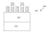
- FIGS. 1-7are sectional views showing one embodiment of a device 100 during various fabrication stages. With reference to FIGS. 1-7 , a method for lithography patterning is described.
- FIG. 1shows a semiconductor device 100 having a silicon substrate 110 .
- the substrate 110may alternatively be made of some other suitable semiconductor material, including Ge, SiGe, or GaAs. Further, the substrate 110 may alternatively be made of some other suitable elementary semiconductor such as diamond; a suitable compound semiconductor such as silicon carbide, indium arsenide, or indium phosphide; or a suitable alloy semiconductor such as silicon germanium carbide, gallium arsenic phosphide, or gallium indium phosphide.
- the substrate 110may include various doped regions, dielectric features, and multilevel interconnects.
- the substrate 110may alternatively be a non-semiconductor material, such as a glass substrate for thin-film-transistor liquid crystal display (TFT-LCD) devices, or fused quartz or calcium fluoride for a photomask (mask or reticle).
- the substrate 110may include a layer to be patterned such as a dielectric layer, a semiconductor layer, or a poly-silicon layer.
- An underlying material layer(also referred to as an “under-material” layer or simply “material” layer) 120 is formed on the substrate 110 .
- the material layer 120may function as a hard mask and/or a bottom anti-reflective coating (BARC).
- BARCbottom anti-reflective coating
- the material layerhas a thickness ranging between about 50 angstroms and 9000 angstroms in one embodiment.
- the thickness of the under-material layer 120can be about 500 angstroms.
- the material layer 120has a thickness ranging between about 1000 angstroms and 3500 angstroms.
- the material layer 120may have other parameters that fall within selected ranges.
- the material layer 120has a refractive index in a range between about 1 and 3, and an extinction coefficient (absorption value) ⁇ in a range between about 0.01 and 1.0.
- the material layer 120may have a refractive index of about 1.75 and an extinction coefficient of about 0.5.
- the material layer 120includes an organic polymer.
- the material layer 120may be substantially free of silicon and/or substantially free of hydroxyl groups and carboxyl groups.
- the material layer 120may include a photoresist (or resist) that is either a positive-type or negative-type, with or without photosensitive material.
- the material layer 120may include a proper BARC material and may further have a top layer to cover the BARC material.
- the top layermay be about 50 angstroms thick, and substantially free of hydroxyl groups and carboxyl groups.
- the material layer 120may include conventional polymer material or resist material.
- the material layermay be one of t-Butyloxycarbonyl (t-BOC) resist, acetal resist, and environmentally stabilized chemically amplified photoresist (ESCAP) that are known in the art.
- the material layer 120 made of polymeric materialthe polymeric material may be cross-linked.
- the polymeric materialcan be spin-on coated to the substrate 110 and then cross-linked using a baking process with temperature ranging between about 90° C. and 300° C. Alternatively, this temperature range could be about 100° C. to 180° C.
- the polymeric materialmay not be cross-linked, and in that case the material layer 120 may use a solvent that is not capable of dissolving a resist layer or not dissolved by the resist layer formed above the material layer 120 .
- the material layer 120may use butanol as a solvent.
- the material layer 120may use other suitable materials that are different from a protective layer that is to be formed above the material layer 120 to protect a resist pattern on the material layer 120 .
- the material layer 120may include silicon nitride or silicon oxynitride in order to be different from a protective layer containing silicon oxide, in which the two layers have substantially different etching rates during an etching process.
- a middle layer 130is formed on the material layer 120 .
- the middle layer 130includes a silicon-containing organic polymer, which may use a solvent different from that of the resist layer.
- the solvent of the middle layeris not capable of dissolving a resist layer.
- the middle layercan use butanol, isobutanol, isopentanol and/or IPA as a solvent.
- the polymeric materialmay be cross-linked.
- the middle layer 130may include a silicon-containing inorganic polymer.
- the inorganic polymeric materialmay include silicon oxide.
- the middle layer 130may include a metal-containing organic polymer material that contains metal such as titanium, titanium nitride, aluminum, and tantalum.
- the middle layer 130may include silicon nitride or silicon oxynitride.
- the middle layer 130may include pure silicon such as polycrystalline silicon or silicon oxide.
- the middle layer 130may include spin-on glass (SOG) known in the art.
- SOGspin-on glass
- the middle layer 130may be thermally baked for cross-linking, thus without further requiring the solvent.
- the middle layer 130may have a thickness ranging between about 500 and 2000 angstroms, or alternatively a range between about 800 and 900 angstroms.
- a patterned resist layer 140is then formed on the middle layer 130 .
- Resist layer 140includes a plurality of openings, such that portions of the middle layer 130 are uncovered within the openings.
- the openings of the resist layer 140are configured according to a predetermined pattern.
- the resist layer 140may have a thickness ranging between about 50 angstroms and 5000 angstroms. Alternatively, the resist layer 140 may have a thickness ranging between about 500 angstroms and 3000 angstroms, or ranging between about 1000 angstroms and 1500 angstroms.
- the resist layer 140can be a positive-type resist or a negative-type resist.
- the resist layer 140may use a chemical amplification (CA) resist.
- CAchemical amplification
- the patterned resist layer 140is formed by a lithography process that may include processing steps of resist coating, soft baking, mask aligning, exposing, post-exposure baking, developing, and hard baking.
- the exposing processmay be carried out by exposing the semiconductor device 100 under a radiation beam through a mask having a predefined pattern (or a reversed pattern).
- the radiation beammay be ultraviolet (UV) or EUV, such as a 248 nm beam from a Krypton Fluoride (KrF) excimer laser, or a 193 nm beam from an Argon Fluoride (ArF) excimer laser.
- the lithography processmay utilize other exposing modes or technologies, such as on-axis, off-axis, quadripole, or dipole exposure technologies.
- the lithography patterningmay alternatively be implemented or replaced by other proper methods such as maskless lithography, electron-beam writing, ion-beam writing, and molecular imprint techniques.
- the patterned resist layer 140may include acid molecular or radiation-sensitive acid generator, such that acid can be generated when a radiation beam is applied.
- the patterned resist layer 140may be further processed using a hardening process.
- the hardening processmay include plasma treatment, ultraviolet (UV) curing, ion implant bombard, e-beam treatment, or combinations thereof.
- a top layer 150is formed on the patterned resist layer 140 and in the openings thereof.
- the top layersubstantially fills the openings in the patterned resist layer 140 .
- the top layer 150substantially covers portions of the middle layer 130 that are exposed within the openings in the patterned resist layer 140 .
- the top layer 150may include a silicon-containing organic polymer, which may use a solvent different from that of the resist layer.
- the solvent of the top layeris not capable of dissolving the resist layer 140 .
- the top layermay utilize an alcohol based solvent.
- the top layercan use butanol, isobutanol, isopentanol and/or IPA as a solvent.
- the polymeric materialmay be cross-linked.
- the top layer 150may include a silicon-containing inorganic polymer.
- the inorganic polymeric materialmay include silicon oxide.
- the top layer 150may alternatively include a metal-containing organic polymer material that contains metal such as titanium, titanium nitride, aluminum, and tantalum.
- the metal-containing material used for the top layermay include Ti, TiN, Al, AlOx, W, WSi, or WOx.
- the top layer 150may include silicon nitride or silicon oxynitride.
- the top layer 150may include pure silicon such as polycrystalline silicon or silicon oxide.
- the top layer 150may include spin-on glass (SOG) known in the art.
- Resist layer 160includes a plurality of openings, such that portions of the top layer 150 are exposed within the openings.
- the patterned resist layer 160may be substantially similar to the resist layer 140 discussed above, in terms of function, formation, and composition.
- the openings in the patterned resist layer 160may be configured relative to the openings of the patterned resist layer 140 so that a double patterning technique can be utilized.
- the openings in the patterned resist layers 140 and 160may be configured to achieve pitch splitting.
- the openings in the patterned resist layers 140 and 160may be configured to form various contact holes.
- an etching processis applied to remove material of the middle layer 130 and the top layer 150 within the openings of the patterned resist layers 140 and 160 .
- the etch processmay use a CF 4 , C 3 F 8 , C 4 F 8 , CHF 3 , or CH 2 F 2 dry etch, or a buffered hydrofluoric acid (BHF) wet etch to etch silicon dioxide in various examples.
- BHFbuffered hydrofluoric acid
- an etching processis applied to the material layer 120 .
- the etching processis chosen so that the material layer 120 has a higher etch rate than the middle layer 130 and the top layer 150 .
- oxygenmay be chosen as the etchant in order to remove the under layer 120 during a plasma etching.
- the patterned resist layers 140 and 160may also be consumed during etching of the material layer 120 .
- the silicon material inside the middle and top layers 130 and 150may react under the oxygen plasma to form silicon oxide, which has a high etching resistance during the etching process.
- the middle layerincludes silicon oxide
- the silicon oxidewould provide an etching resistance.
- the middle and top layersinclude titanium, titanium nitride, tantalum, aluminum, metal ion, metal complex, organic metal, or a combination thereof, then metal oxide may be formed and provide an etching resistance.
- the etching processmay alternatively be implemented using a nitrogen plasma or a mixture of oxygen, hydrogen, carbon fluoride, carbon bromide and nitrogen plasma, during which silicon-containing material in the middle and/or top layers will be transformed into an associated nitride or oxynitride.
- the substrate 110is etched through the patterned material layer 120 to form a plurality of trenches, using a suitable etching process including a dry etch or a wet etch. At least some of the material layer 120 may be consumed during the etching process. The remainder of the material layer 120 is thereafter removed, as illustrated in FIG. 7 .
- the method described above with reference to FIGS. 1 to 7provides a double patterning process. This process achieves double exposure and single etch to the middle and top layers. This can reduce manufacturing cost and minimize CD variation.
- the processmay be utilized in various applications.
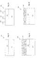
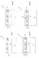
- a plurality of contact holesmay be formed, as illustrated in various fabrication stages in the top views of FIGS. 8 a to 13 a , and the corresponding sectional views of FIGS. 8 b to 13 b .
- a plurality of line features with split pitchmay be formed, as illustrated in various fabrication stages in the top views of FIGS. 14 a to 19 a , and the corresponding sectional views of FIGS. 14 b to 19 b.
- the top layer 150 used in the above-described processis further explained in association with FIG. 20 .
- the top layer 150may have a refractive index ranging from about 1.1 to 1.9 and a absorption value ranging from about 0.001 to 0.8. In one example, the refractive index is about 1.8, and the absorption value is about 0.2.
- the top layer 150may have a silicon content that is more than about 20% by weight.
- the top layer 150may also have a cure temperature that is less than about 150° C.
- the top layer 150includes a first polymer 152 .
- the first polymer 152further includes a functional unit “f” capable of enhancing etching resistance during an etching process.
- This functional unit fmay include a tertiary carbon structure, a double bond, a triple bond, or combinations thereof.
- the first polymer 152also includes a reaction unit “c” that is capable of reacting to a cross-linker.
- the reaction unit cmay include a functional group such as OH, COOH, anhydride, or combinations thereof.
- the first polymer 152may include a backbone unit such as those illustrated in FIGS. 21 a and 21 b .
- the backbone units Si—O or Si—Sican be repeated and/or combined.
- FIG. 21 a and 21 bThe backbone units Si—O or Si—Si can be repeated and/or combined.
- R1 to R6may each be hydrogen, a halide atom, a straight alkyl, a branched alkyl, a cyclic alkyl, a fluorinated alkyl group, a silicon oxide alkyl, or a silicon alkyl of about 1 to 10000 atom unit.
- R1 to R6may each be hydrogen, a fluorine atom, a straight alkyl, a branched alkyl, cyclic alkyl, a fluorinated alkyl group, a silicon oxide alkyl, or a silicon alkyl of about 1 to 10000 atom unit.
- the top layer 150further includes a cross-linker 154 with various reaction units “d” capable of reacting with the first polymer 152 and other polymers if present.
- the reaction unit dmay include a functional group such as OH, COOH, anhydride, or combinations thereof.
- the cross-linking temperature(cure temperature) ranges between about 100° C. and 250° C.
- the baking temperaturemay be about 150° C., for example.
- the cross-linker 154may include N((CH 2 )xOH)y where the parameter x has a range from 1 to 10 and parameter y has a range from 1 to 4.
- Exemplary interactions between the polymer and the cross-linkermay include R1OCH3+R2OH—>R1OR2+HOCH3 or R1OH+R2OH—>R1OR2+H2O.
- the top layer 150may include a second polymer 156 .
- the second polymer 156includes a functional unit “e” capable of absorbing imaging light during an etching process.
- the functional unit emay include a double bond, a triple bond, or combinations thereof.
- the functional unit eincludes a benzyl group, phenyl group, or substitute benzyl group.
- the second polymer 156also includes a reaction unit “c” capable of reacting to the cross-linker 154 .
- the second polymer 156includes a backbone unit similar to those illustrated in FIGS. 21 a and 21 b and described above.
- FIG. 22is a flowchart showing an embodiment of a method 200 of lithography patterning, which is the lithography patterning described above in association with FIGS. 1-7 .
- the method 200begins at step 202 by forming an underlying material layer on a substrate, and then continues at step 204 by forming a middle layer on the under material layer.
- a first patterned resist layeris formed on the middle layer.
- a top layeris formed on the first patterned resist layer, and at step 210 a second patterned resist layer is formed on the top layer.
- the top and middle layersare etched using the first and second patterned resist layers as a mask.
- the underlying material layeris etched using the patterned top and middle layers as a mask.
- the substrateis etched using the underlying material layer as a hard mask.
- FIGS. 23 to 34are sectional views showing a further device 300 at respective different stages of fabrication, where the device 300 is an alternative embodiment of the device 100 shown in FIGS. 1-7 .
- a method for lithography patterningis disclosed.
- FIG. 23shows that the semiconductor device 300 includes a silicon substrate 310 .
- the substrate 310may alternatively be made of some other suitable material, for example as described above in association with the substrate 110 .
- An underlying material layer 320is formed on the substrate 310 .
- the material layer 320is chosen so that it is substantially different from a hard mask layer subsequently formed above it in terms of etching rate.
- the material layer 320may be made of a material substantially similar to that described above for the material layer 120 .
- the material layer 320may alternatively include a multilayer structure.
- the material layer 320may include a first polymer layer and a second polymer layer disposed on the first polymer layer.
- the second polymer layermay include a radiation-sensitive material sensitive to the radiation beam of an exposure system such as an ultraviolet, extreme ultraviolet (EUV), or electron-beam system.
- EUVextreme ultraviolet
- a patterned resist layer 330is formed on the underlying material layer 320 .
- the resist layer 330has a plurality of openings, such that portions of the material layer 320 are exposed within the openings.
- the patterned resist layer 330may be substantially similar to the resist layer 130 described above, in terms of function, formation, configuration, and composition.
- a hard mask layer 340is formed on the patterned resist layer 330 , and in the openings thereof.
- the hard mask layersubstantially fills the openings of the patterned resist layer 330 , and thus substantially covers the portions of the underlying material layer 320 exposed within the openings of the patterned resist layer 330 .
- the hard mask layer 340includes a silicon-containing organic polymer, which may use a solvent different from that of the resist layer.
- the solvent of the hard mask layeris not capable of dissolving the resist layer 330 .
- the hard mask layermay use an alcohol based solvent.
- the hard maskcan use butanol, isobutanol, isopentanol and/or IPA as a solvent.
- the silicon-containing organic polymermay include silsesquioxane (SSQ).
- the polymeric materialmay be cross-linked.
- the hard mask layer 340may include a silicon-containing inorganic polymer.
- the inorganic polymeric materialmay include silicon oxide.
- the hard mask layermay alternatively include a metal-containing organic polymer material that contains metal such as titanium, titanium nitride, aluminum, and tantalum.
- the hard mask layer 340may include silicon nitride or silicon oxynitride.
- the hard mask layer 340may include pure silicon, such as polycrystalline silicon or silicon oxide.
- the hard mask layer 340may include spin-on glass (SOG), known in the art.
- the hard mask layer 340may be similar to the top layer 150 of FIG. 2 or FIG. 20 .
- an etching processis applied to etch back the hard mask layer sufficiently so that the top surfaces of the patterned resist layer 330 are substantially exposed.
- the etch back processmay use a CF 4 dry etch, or a buffered hydrofluoric acid (BHF) wet etch to etch silicon dioxide.
- BHFbuffered hydrofluoric acid
- Some other proper etchants or processesmay be utilized to achieve the etching back, such as chemical mechanical polishing (CMP) process.
- the patterned resist layer 330is removed, for example by a conventional process that can include wet stripping or oxygen plasma stripping.
- a reversed hard mask patternis formed, in which the openings within the hard mask layer 340 are covered by the patterned resist layer 330 before the removal of the resist layer 330 .
- the methodcan continue by etching the under layer 320 through the openings in the hard mask layer 340 , and then etching the substrate 310 using the under layer 320 as a mask.
- a procedure similar to that discussed abovecan be used to form another reverse pattern, as will now be described.
- another patterned resist layer 350is formed on the patterned hard mask layer 340 , and on the portions of the material layer 320 exposed within the openings of the hard mask layer 340 .
- the resist layer 350includes a plurality of openings that expose portions of the material layer 320 .
- the patterned resist layer 350may be substantially similar to the resist layer 330 discussed above, in terms of function, formation, and composition.
- another hard mask layer 360is formed on the patterned resist layer 350 , and substantially fills the openings in the patterned resist layer 350 .
- the hard mask layer 360substantially covers portions of the underlying material layer 320 that are exposed within the openings of the patterned resist layer 350 .
- the hard mask layer 360includes a silicon-containing organic polymer, which may use a solvent different from that of the resist layer.
- the solvent of the hard mask layeris not capable of dissolving the resist layer 350 .
- the hard maskcan use butanol, isobutanol, isopentanol and/or IPA as a solvent.
- the polymeric materialmay be cross-linked.
- the hard mask layer 360may include a silicon-containing inorganic polymer.
- the inorganic polymeric materialmay include silicon oxide.
- the hard mask layermay alternatively include a metal-containing organic polymer material that contains a metal such as titanium, titanium nitride, aluminum, or tantalum.
- the hard mask layer 360may include silicon nitride or silicon oxynitride.
- the hard mask layer 360may include pure silicon such as polycrystalline silicon or silicon oxide.
- the hard mask layer 360may include spin-on glass (SOG), known in the art.
- SOGspin-on glass
- the hard mask layer 360may be similar to the hard mask layer 340 .
- an etching processis applied to etch back the hard mask layer 360 sufficiently so that the top surfaces of the patterned resist layer 350 are substantially exposed.
- the etch back processmay, for example, use a CF 4 dry etch, or a buffered hydrofluoric acid (BHF) wet etch to etch silicon dioxide.
- BHFbuffered hydrofluoric acid
- Other proper processmay be utilized to implement the etch back, such as chemical mechanical polishing (CMP).
- the patterned resist layer 350is removed, for example by a conventional process that includes wet stripping or oxygen plasma stripping.
- a reversed hard mask patternis formed, in which the under layer 320 is exposed within the openings of the patterned hard mask layers 340 and 360 .
- the reversed hard mask patterncan be trimmed to reduce the widths of the hard mask islands, for realizing small feature sizes.
- another resist layermay be applied and patterned such that a trimming process may be performed to modify the hard mask pattern within particular regions. For example, isolated trenches may be thus modified to eliminate an etching load effect.
- Such a reversed hard mask patterncan be incorporated into lithography patterning technologies.
- the reversed hard mask patternmay be integrated with chromeless phase lithography.
- the chromeless phase lithographyhas high optical contrast.
- the chromeless maskcan print better images than PSM or a binary mask.
- a chromeless maskcan print an island pattern by using a positive resist.
- the reverse hard mask patternis capable of transferring the island pattern to a hole pattern with improved resolution.
- the methodnot only reverses the image pattern, but also improves the etch resistance.
- a silicon-containing layercan be used as a hard mask in transferring the reversed pattern to the under layer.
- the good etching selectivity of the silicon-containing layer with respect to the under layerenables the under layer to have a high aspect ratio.
- the under layer with a high thicknesscan achieve substrate patterning while eliminating pattern collapse and other issues.
- the reversed hard mask pattern utilized with double patterning techniquescan be used in various applications. For example, if a line pattern can be achieved with better quality through the reversed pattern with the double patterning technique, then various contact holes can be formed with enhanced resolution.
- an etching processis applied to open the underlying material layer 320 if it is formed on the substrate 310 .
- An etching processis chosen such that the underlying material layer 320 has a higher etch rate relative to the etch rate of the hard mask layers 340 and 360 .
- a hot phosphoric acidH 3 PO 4
- H 3 PO 4can be used to selectively remove the underlying material layer 320 .
- another etching processis applied to etch the substrate 310 under the patterned underlying material layer 320 .
- This etching processis chosen so that the substrate 310 is selectively etched.
- the hard mask layer 340 and 360is removed before the etching of the substrate 310 .
- the hard mask layer 340 and 360may be removed along with the material layer 320 after the etching of the substrate 310 .
- the etching processis chosen so that the etchant has a higher etch rate for the substrate 310 than for the hard mask layer 340 and 360 .
- the under layer 320may be subsequently removed by an etching process, as illustrated in FIG. 34 .
- FIG. 35is a flowchart of a method 400 for lithography patterning, where the method 400 implements the lithography patterning technique described above with respect to FIGS. 23-34 .
- the method 400begins at step 402 by forming an under material layer on a substrate, and then continues in step 404 by forming a first patterned resist layer on the underlying material layer.
- step 406a first hard mask layer is formed on the first patterned resist layer, and in step 408 , the first hard mask layer is etched back to expose the top surfaces of the first patterned resist layer.
- the first patterned resist layeris removed.
- step 412a second patterned resist layer is formed on the first patterned hard mask layer and on portions of the underlying material layer exposed within the openings of the first patterned hard mask layer.
- step 414a second hard mask layer is formed on the second patterned resist layer.
- step 416the second hard mask layer is etched back to expose the top surfaces of the second patterned resist layer, and then in step 418 the second patterned resist layer is removed.
- step 420the under material layer exposed within the openings of the hard mask layers is etched.
- step 422the substrate exposed within the openings of the under material layer is etched.
- the hard mask layers, the patterned resist layer, and the underlying material layerare removed, as described in association with FIGS. 23-34 .
- the under material layermay be alternatively avoided.
- a lithography patterning method and a top layer materialhave been introduced and described. Other modifications, variations, additions, and extensions may be used without departing from the scope of the disclosure.
- a hardening processmay be applied to one resist layer using a plasma treatment, UV curing, ion implantation, or e-beam treatment.
- a top layer, a middle layer, or an under layermay be cross-linked (or cured) if necessary.
- a resist layer and a silicon-containing (or metal-containing) materialmay use a different solvent to avoid mixing or interdiffusion.
- a resist layermay use an organic solvent such as propylene glycol monomethyl ether (PGME) or propylene glycol monomethyl ether acetate (PGMEA), while the top layer may use an alcohol solvent such as butanol, isobutanol, pentanol, isopentanol, and/or IPA. All of the above techniques that include hardening, cross-linking, and utilizing different solvents may be alternatively implemented, or combined, depending on the configuration and the processing procedure.
- organic solventsuch as propylene glycol monomethyl ether (PGME) or propylene glycol monomethyl ether acetate (PGMEA)
- PGMEpropylene glycol monomethyl ether acetate
- IPAIPA
- the present disclosureprovides a method of lithography patterning.
- the method of lithography double patterningincludes forming a first material layer on a substrate; forming a first patterned resist layer including at least one opening therein on the first material layer; forming a second material layer on the first patterned resist layer and the first material layer; forming a second patterned resist layer including at least one opening therein on the second material layer; and etching the first and second material layers uncovered by the first and second patterned resist layers.
- the first and second material layerseach may include one of a silicon-containing material and a metal-containing material.
- the first and second material layerseach may include a chemical unit selected from the group consisting of Si, Ti, TiN, Ta, Al, a metal ion, a metal complex, an organic metal, and combinations thereof.
- the methodmay further include forming a third material on the substrate before the forming of the first material layer.
- the forming of the third material layermay include forming a polymeric material selected from the group consisting of organic polymer, resist, BARC, and combinations thereof.
- the methodmay further include etching the third material layer uncovered by the first and second material layers after the etching of the first and second material layers.
- the methodmay further include etching the substrate using the third material layer as a hard mask after the etching of the third material layer.
- the etching of the third material layermay include using a plasma etchant selected from the group consisting of oxygen plasma, nitrogen plasma, hydrogen, alkyl halide, and combinations thereof.
- the forming of the first material layermay include forming a material having a refractive index ranging between about 1.1 and 1.9, and an absorption value ranging between about 0.01 and 0.8.
- the forming of the patterned resist layermay include exposing the patterned resist layer utilizing a means selected from a group consisting of a Krypton Fluoride (KrF) excimer laser, an Argon Fluoride (ArF) excimer laser, extreme ultraviolet (EUV) technology, imprint technology, electron-beam technology, and combinations thereof.
- the forming of each of the first and second material layersmay include providing a cross-linking polymeric material.
- the providing of the cross-linking polymeric materialmay include diffusing acid from the patterned resist layer to the second material layer or a baking process with a temperature in the range between about 25° C. and 150° C.
- the forming of one of the first and second material layersmay include utilizing a hardening process.
- the present disclosurealso provides another method of lithography patterning.
- the methodincludes forming a first material layer on a substrate; forming a first patterned resist layer including at least one opening therein on the first material layer; forming a second material layer within the patterned resist layer, the second material layer being different from the first material layer; and removing the first patterned resist layer to form a pattern of the second material layer being complementary to the first patterned resist layer.
- the disclosed methodmay further include opening the first material layer using the pattern of the second material layer as a mask, and may further include etching the substrate within openings of the first material layer.
- the first materialmay be substantially free of silicon and the second material may contain silicon.
- the first materialmay be substantially free of metal and the second material may contain metal.
- the second material layermay include a component selected from the group consisting of an organic polymer, an inorganic material, and a solvent system different from that of the first patterned resist layer.
- the second materialmay include cross-linkers.
- the methodmay further include cross-linking the second material by a thermal baking.
- the methodmay further include hardening the first patterned resist layer before the forming of the second material layer.
- the methodmay further include implementing an etch-back process to the second material layer before the removing of the first patterned resist layer.
- the methodmay further include forming a second patterned resist layer including at least one opening therein on the pattern of the second material and the substrate; forming a third material layer within the at least one opening of the second patterned resist layer; and removing the second patterned resist layer to form a pattern of the third material being complementary to the second patterned resist layer.
- the third material layermay be substantially similar to the first material layer.
- the methodmay further include opening the first material layer using the second and the third material layers as a mask.
- the forming of the first material layermay include forming a material having a refractive index ranging between about 1.1 and 1.9, and an absorption value ranging between about 0.001 and 0.8.
- the present disclosurealso provides another method including: forming a first patterned resist layer including at least one opening therein on a substrate; forming a first hard mask layer on the first patterned resist layer; etching back the first hard mask layer to expose the first patterned resist layer; removing the first patterned resist layer; forming a second patterned resist layer including at least one opening therein on the first hard mask layer and the substrate; forming a second hard mask layer on the second patterned resist layer and the substrate; etching back the second hard mask layer to expose the second patterned resist layer; and removing the second patterned resist layer.
- the disclosed methodmay further include etching the substrate uncovered by the first and second hard mask layers.
- the etching back one of the first and second hard mask layersmay include a process selected from a dry etching, a wet etching, or a combination thereof.
- the first and second hard mask layerseach may include at least one of Si, Ti, TiN, Al, and Ta.
- the forming of one of the first and second hard mask layersmay include forming a material selected from the group consisting of silicon, silicon oxide, silicon nitride, silicon oxynitride, and combinations thereof.
- the forming one of the first and second hard mask layersmay include forming a silicon-containing organic polymer.
- the forming of the silicon-containing organic polymermay include cross-linking the silicon-containing organic polymer.
- the forming one of the first and second hard mask layersmay include forming a silicon-containing inorganic polymer.
- the silicon-containing inorganic polymermay include silicon oxide.
- the forming one of the first and second hard mask layersmay include a process selected from spin-on coating and chemical vapor deposition (CVD).
- the methodmay further include an etching process to trim the hard mask layer.
- the present disclosurealso provides a material utilized in photolithography patterning.
- the materialincludes: a solvent consisting of one of isobutanol and isopentanol; and a first polymer that has a first functional unit capable of enhancing etching resistance and at least one of silicon and a metal.
- the disclosed materialmay further include a cross-linker with a plurality of first reaction units.
- Each first reaction unitmay include a functional group selected from the group consisting of OH, COOH, anhydride, and combinations thereof.
- the first polymermay further include a second reaction unit.
- the second reaction unitmay include a functional group selected from the group consisting of OH, COOH, anhydride, and combinations thereof.
- the materialmay further include a second polymer having a second functional unit capable of absorbing imaging light.
- the second functional unitmay include at least one of a double bond, a triple bond, a tertiary carbon structure, and combinations thereof.
- the second functional unitmay include one of a benzyl group, a phenyl group, and combinations thereof.
- the second polymermay further include at least one of silicon and a metal.
- the first and second polymerseach may include a backbone unit selected from the group consisting of Si—O—Si, Si—Si, and combinations thereof.
- the first and second polymerseach may further include various units selected from the group consisting of hydrogen, halide, a straight alkyl, a branched alkyl, a cyclic alkyl, fluorinated alkyl, silicon contain alkyl, silicon oxide contain alkyl, and combinations thereof, each being attached to the backbone unit.
- the first functional unitmay include at least one of a double bond, a triple bond, tertiary carbon structure, and combinations thereof.
Landscapes
- Engineering & Computer Science (AREA)
- Physics & Mathematics (AREA)
- Condensed Matter Physics & Semiconductors (AREA)
- General Physics & Mathematics (AREA)
- Computer Hardware Design (AREA)
- Microelectronics & Electronic Packaging (AREA)
- Power Engineering (AREA)
- Manufacturing & Machinery (AREA)
- Internal Circuitry In Semiconductor Integrated Circuit Devices (AREA)
- Drying Of Semiconductors (AREA)
- Photosensitive Polymer And Photoresist Processing (AREA)
Abstract
Description
Claims (20)
Priority Applications (2)
| Application Number | Priority Date | Filing Date | Title |
|---|---|---|---|
| US12/814,172US8258056B2 (en) | 2006-03-22 | 2010-06-11 | Method and material for forming a double exposure lithography pattern |
| US13/599,143US8658532B2 (en) | 2006-03-22 | 2012-08-30 | Method and material for forming a double exposure lithography pattern |
Applications Claiming Priority (3)
| Application Number | Priority Date | Filing Date | Title |
|---|---|---|---|
| US78466006P | 2006-03-22 | 2006-03-22 | |
| US11/457,032US7767570B2 (en) | 2006-03-22 | 2006-07-12 | Dummy vias for damascene process |
| US12/814,172US8258056B2 (en) | 2006-03-22 | 2010-06-11 | Method and material for forming a double exposure lithography pattern |
Related Parent Applications (3)
| Application Number | Title | Priority Date | Filing Date |
|---|---|---|---|
| US11/457,032DivisionUS7767570B2 (en) | 2006-03-22 | 2006-07-12 | Dummy vias for damascene process |
| US11/563,805DivisionUS7759253B2 (en) | 2006-03-22 | 2006-11-28 | Method and material for forming a double exposure lithography pattern |
| US12/563,805DivisionUS8398594B2 (en) | 2007-03-22 | 2009-09-21 | Spring arrangement in an injection device |
Related Child Applications (1)
| Application Number | Title | Priority Date | Filing Date |
|---|---|---|---|
| US13/599,143ContinuationUS8658532B2 (en) | 2006-03-22 | 2012-08-30 | Method and material for forming a double exposure lithography pattern |
Publications (2)
| Publication Number | Publication Date |
|---|---|
| US20110008968A1 US20110008968A1 (en) | 2011-01-13 |
| US8258056B2true US8258056B2 (en) | 2012-09-04 |
Family
ID=38534031
Family Applications (4)
| Application Number | Title | Priority Date | Filing Date |
|---|---|---|---|
| US11/457,032Active2026-12-18US7767570B2 (en) | 2006-03-22 | 2006-07-12 | Dummy vias for damascene process |
| US12/716,980Expired - Fee RelatedUS7960821B2 (en) | 2006-03-22 | 2010-03-03 | Dummy vias for damascene process |
| US12/814,172Expired - Fee RelatedUS8258056B2 (en) | 2006-03-22 | 2010-06-11 | Method and material for forming a double exposure lithography pattern |
| US13/599,143ActiveUS8658532B2 (en) | 2006-03-22 | 2012-08-30 | Method and material for forming a double exposure lithography pattern |
Family Applications Before (2)
| Application Number | Title | Priority Date | Filing Date |
|---|---|---|---|
| US11/457,032Active2026-12-18US7767570B2 (en) | 2006-03-22 | 2006-07-12 | Dummy vias for damascene process |
| US12/716,980Expired - Fee RelatedUS7960821B2 (en) | 2006-03-22 | 2010-03-03 | Dummy vias for damascene process |
Family Applications After (1)
| Application Number | Title | Priority Date | Filing Date |
|---|---|---|---|
| US13/599,143ActiveUS8658532B2 (en) | 2006-03-22 | 2012-08-30 | Method and material for forming a double exposure lithography pattern |
Country Status (2)
| Country | Link |
|---|---|
| US (4) | US7767570B2 (en) |
| TW (1) | TWI329908B (en) |
Cited By (3)
| Publication number | Priority date | Publication date | Assignee | Title |
|---|---|---|---|---|
| US20120329282A1 (en)* | 2006-03-22 | 2012-12-27 | Taiwan Semiconductor Manufacturing Company, Ltd. | Method and material for forming a double exposure lithography pattern |
| US9123656B1 (en) | 2014-05-13 | 2015-09-01 | Taiwan Semiconductor Manufacturing Co., Ltd. | Organosilicate polymer mandrel for self-aligned double patterning process |
| US12022645B2 (en) | 2020-10-20 | 2024-06-25 | Samsung Electronics Co., Ltd. | Methods of manufacturing semiconductor device |
Families Citing this family (51)
| Publication number | Priority date | Publication date | Assignee | Title |
|---|---|---|---|---|
| JP2008159608A (en)* | 2006-12-20 | 2008-07-10 | Fujitsu Ltd | Semiconductor device, semiconductor device manufacturing method, and semiconductor device design apparatus |
| KR100877096B1 (en)* | 2006-12-29 | 2009-01-09 | 주식회사 하이닉스반도체 | Semiconductor device having dummy pattern and method for forming same |
| US7470624B2 (en)* | 2007-01-08 | 2008-12-30 | Freescale Semiconductor, Inc. | Integrated assist features for epitaxial growth bulk/SOI hybrid tiles with compensation |
| JP2009060034A (en)* | 2007-09-03 | 2009-03-19 | Rohm Co Ltd | Semiconductor device |
| KR20100006756A (en)* | 2008-07-10 | 2010-01-21 | 삼성전자주식회사 | Semiconductor device and method of fabricating the same |
| US8822347B2 (en)* | 2009-04-27 | 2014-09-02 | Taiwan Semiconductor Manufacturing Company, Ltd. | Wet soluble lithography |
| US8304179B2 (en)* | 2009-05-11 | 2012-11-06 | Taiwan Semiconductor Manufacturing Company, Ltd. | Method for manufacturing a semiconductor device using a modified photosensitive layer |
| US8470711B2 (en)* | 2010-11-23 | 2013-06-25 | International Business Machines Corporation | Tone inversion with partial underlayer etch for semiconductor device formation |
| US8835217B2 (en)* | 2010-12-22 | 2014-09-16 | Intel Corporation | Device packaging with substrates having embedded lines and metal defined pads |
| JP6039886B2 (en)* | 2011-04-08 | 2016-12-07 | 富士通株式会社 | Manufacturing method of semiconductor device |
| CN102969269A (en)* | 2011-08-31 | 2013-03-13 | 上海华力微电子有限公司 | Semiconductor device and production method thereof |
| KR20130046664A (en)* | 2011-10-28 | 2013-05-08 | 삼성전자주식회사 | Methods of forming a pattern and methods of manufacturing a semiconductor device using the same |
| CN102446845A (en)* | 2011-11-28 | 2012-05-09 | 上海华力微电子有限公司 | Method for improving wafer warpage deformation induced by super-thick top metal |
| CN102437107A (en)* | 2011-11-29 | 2012-05-02 | 上海华力微电子有限公司 | Method for manufacturing integrated circuit with super-thick top-layer metal and integrated circuit |
| KR101841199B1 (en) | 2011-12-07 | 2018-03-23 | 삼성전자주식회사 | Method of forming semiconductor device and the device formed by the method |
| WO2013101028A1 (en)* | 2011-12-29 | 2013-07-04 | Intel Corporation | Avd hardmask for damascene patterning |
| TWI550713B (en)* | 2012-01-18 | 2016-09-21 | 聯華電子股份有限公司 | Method for manufacturing damascene structure |
| US8883638B2 (en)* | 2012-01-18 | 2014-11-11 | United Microelectronics Corp. | Method for manufacturing damascene structure involving dummy via holes |
| JP5870833B2 (en)* | 2012-04-24 | 2016-03-01 | 富士通セミコンダクター株式会社 | Manufacturing method of semiconductor device |
| CN102738076B (en)* | 2012-07-27 | 2014-10-22 | 上海华力微电子有限公司 | Through hole propriety copper interconnection manufacturing method |
| CN102810509A (en)* | 2012-08-16 | 2012-12-05 | 上海华力微电子有限公司 | Preparation process of dual-damascene shallow-redundancy metal |
| FR3003962B1 (en)* | 2013-03-29 | 2016-07-22 | St Microelectronics Rousset | METHOD FOR PRODUCING A PHOTOLITOGRAPHY MASK FOR THE FORMATION OF CORRESPONDING CONTACTS, MASK AND INTEGRATED CIRCUIT |
| US20150171008A1 (en)* | 2013-12-17 | 2015-06-18 | GLOBAL FOUNDRIES Singapore Ptd. Ltd. | Integrated circuits with dummy contacts and methods for producing such integrated circuits |
| US9196583B1 (en)* | 2014-05-09 | 2015-11-24 | Qualcomm Incorporated | Via material selection and processing |
| US9570341B2 (en)* | 2014-05-15 | 2017-02-14 | Taiwan Semiconductor Manufacturing Company, Ltd. | Semiconductor device having air gap structures and method of fabricating thereof |
| US9496224B2 (en) | 2014-05-15 | 2016-11-15 | Taiwan Semiconductor Manufacturing Company, Ltd. | Semiconductor device having air gap structures and method of fabricating thereof |
| US9791779B2 (en) | 2014-10-16 | 2017-10-17 | Tokyo Electron Limited | EUV resist etch durability improvement and pattern collapse mitigation |
| JP6521263B2 (en)* | 2014-10-21 | 2019-05-29 | 日産化学株式会社 | Resist underlayer film forming composition |
| US9379327B1 (en) | 2014-12-16 | 2016-06-28 | Carbonics Inc. | Photolithography based fabrication of 3D structures |
| US9543165B2 (en)* | 2015-02-13 | 2017-01-10 | Taiwan Semiconductor Manufacturing Company, Ltd. | Method of fabricating semiconductor device |
| KR102325201B1 (en)* | 2015-04-22 | 2021-11-11 | 삼성전자주식회사 | Methods of manufacturing semiconductor devices |
| US9685507B2 (en) | 2015-06-25 | 2017-06-20 | International Business Machines Corporation | FinFET devices |
| CN105374746B (en)* | 2015-12-03 | 2018-05-29 | 上海集成电路研发中心有限公司 | A kind of method for promoting via layer process window |
| US10627720B2 (en)* | 2017-08-18 | 2020-04-21 | Globalfoundries Inc. | Overlay mark structures |
| DE102018104644A1 (en)* | 2017-08-30 | 2019-02-28 | Taiwan Semiconductor Manufacturing Co., Ltd. | SEMICONDUCTOR COMPONENT AND ITS MANUFACTURING METHOD |
| US10573519B2 (en)* | 2017-09-08 | 2020-02-25 | Taiwan Semiconductor Manufacturing Co., Ltd. | Method for performing a photolithography process |
| US10990013B2 (en)* | 2017-09-22 | 2021-04-27 | Taiwan Semiconductor Manufacturing Co., Ltd. | Method for forming semiconductor structure |
| US11009796B2 (en)* | 2017-09-22 | 2021-05-18 | Taiwan Semiconductor Manufacturing Co., Ltd. | Method for forming semiconductor structure |
| US10727045B2 (en)* | 2017-09-29 | 2020-07-28 | Taiwan Semiconductor Manufacturing Company, Ltd. | Method for manufacturing a semiconductor device |
| US10741391B2 (en)* | 2017-10-25 | 2020-08-11 | Taiwan Semiconductor Manufacturing Co., Ltd. | Method for forming semiconductor structure by patterning resist layer having inorganic material |
| US10684545B2 (en)* | 2017-11-17 | 2020-06-16 | Taiwan Semiconductor Manufacturing Co., Ltd. | Method for forming semiconductor structure by patterning assist layer having polymer |
| CN110707044B (en) | 2018-09-27 | 2022-03-29 | 联华电子股份有限公司 | Method for forming semiconductor device layout |
| CN110707004B (en)* | 2018-10-11 | 2022-02-18 | 联华电子股份有限公司 | Semiconductor device and method of forming the same |
| US11694984B2 (en) | 2019-08-30 | 2023-07-04 | Advanced Semiconductor Engineering, Inc. | Package structure including pillars and method for manufacturing the same |
| US11158572B2 (en) | 2019-08-30 | 2021-10-26 | Advanced Semiconductor Engineering, Inc. | Package structure including a first electronic device, a second electronic device and a plurality of dummy pillars |
| KR20220111245A (en)* | 2019-12-12 | 2022-08-09 | 인텔 코포레이션 | Dummy wordline contacts to improve the etch margin of semi-isolated wordlines in step structures |
| US11049764B1 (en) | 2019-12-12 | 2021-06-29 | United Microelectronics Corp. | Method for fabricating a semiconductor device |
| US11742309B2 (en)* | 2020-08-21 | 2023-08-29 | Micron Technology, Inc. | Bump coplanarity for semiconductor device assembly and methods of manufacturing the same |
| CN116936464A (en) | 2022-04-08 | 2023-10-24 | 联华电子股份有限公司 | Semiconductor components and manufacturing methods |
| TWI885271B (en) | 2022-06-21 | 2025-06-01 | 聯華電子股份有限公司 | Semiconductor structure |
| US20250125253A1 (en)* | 2023-10-16 | 2025-04-17 | Samsung Electronics Co., Ltd. | Bridge-free and cmp-friendly interconnect structure in semiconductor device |
Citations (44)
| Publication number | Priority date | Publication date | Assignee | Title |
|---|---|---|---|---|
| US4426247A (en) | 1982-04-12 | 1984-01-17 | Nippon Telegraph & Telephone Public Corporation | Method for forming micropattern |
| US5858620A (en) | 1996-07-05 | 1999-01-12 | Mitsubishi Denki Kabushiki Kaisha | Semiconductor device and method for manufacturing the same |
| US6207576B1 (en)* | 1999-01-05 | 2001-03-27 | Advanced Micro Devices, Inc. | Self-aligned dual damascene arrangement for metal interconnection with low k dielectric constant materials and oxide etch stop layer |
| US6277752B1 (en) | 1999-06-28 | 2001-08-21 | Taiwan Semiconductor Manufacturing Company | Multiple etch method for forming residue free patterned hard mask layer |
| US6296780B1 (en)* | 1997-12-08 | 2001-10-02 | Applied Materials Inc. | System and method for etching organic anti-reflective coating from a substrate |
| US6361928B1 (en) | 2000-03-04 | 2002-03-26 | United Microelectronics Corp. | Method of defining a mask pattern for a photoresist layer in semiconductor fabrication |
| US20020036183A1 (en) | 2000-09-27 | 2002-03-28 | Kabushiki Kaisha Toshiba | Method for forming pattern |
| US20020064958A1 (en) | 2000-10-19 | 2002-05-30 | Koichi Takeuchi | Exposure method |
| US6436587B1 (en)* | 2000-09-18 | 2002-08-20 | Sharp Laboratories Of America, Inc. | Method of making a multi-level reticle using bi-level photoresist, including a phase-shifted multi-level reticle |
| US6492075B1 (en) | 2000-06-16 | 2002-12-10 | Advanced Micro Devices, Inc. | Chemical trim process |
| US20030003716A1 (en) | 2001-06-27 | 2003-01-02 | Hynix Semiconductor Inc. | Method for forming dual damascene line structure |
| US6536063B1 (en) | 1997-07-17 | 2003-03-25 | Igus Spritzgussteile für die Industrie GmbH | Guide channel structure |
| US6576562B2 (en) | 2000-12-15 | 2003-06-10 | Kabushiki Kaisha Toshiba | Manufacturing method of semiconductor device using mask pattern having high etching resistance |
| US6593063B1 (en) | 1999-08-26 | 2003-07-15 | Mitsubishi Denki Kabushiki Kaisha | Method of manufacturing a semiconductor device having an improved fine structure |
| US20030134231A1 (en) | 2002-01-15 | 2003-07-17 | Taiwan Semiconductor Manufacturing Co., Ltd. | Bi-layer photoresist dry development and reactive ion etch method |
| US6605413B1 (en)* | 2001-03-29 | 2003-08-12 | Advanced Micro Devices, Inc. | Chemical treatment to strengthen photoresists to prevent pattern collapse |
| US6660456B2 (en)* | 2001-06-27 | 2003-12-09 | International Business Machines Corporation | Technique for the size reduction of vias and other images in semiconductor chips |
| US20040033445A1 (en) | 2002-08-14 | 2004-02-19 | Sung-Ho Lee | Method of forming a photoresist pattern and method for patterning a layer using a photoresist |
| US6780708B1 (en)* | 2003-03-05 | 2004-08-24 | Advanced Micro Devices, Inc. | Method of forming core and periphery gates including two critical masking steps to form a hard mask in a core region that includes a critical dimension less than achievable at a resolution limit of lithography |
| US6830850B1 (en)* | 2001-03-16 | 2004-12-14 | Advanced Micro Devices, Inc. | Interferometric lithography using reflected light from applied layers |
| US20050197721A1 (en) | 2004-02-20 | 2005-09-08 | Yung-Cheng Chen | Control of exposure energy on a substrate |
| US20050260848A1 (en) | 2004-05-21 | 2005-11-24 | Molecular Imprints, Inc. | Method of forming a recessed structure employing a reverse tone process |
| US7087498B2 (en)* | 2003-09-30 | 2006-08-08 | Agere Systems Inc. | Method for controlling trench depth in shallow trench isolation features |
| US20060257791A1 (en) | 2005-05-16 | 2006-11-16 | Hynix Semiconductor Inc. | Method for forming conductive line of semiconductor device |
| US20070037410A1 (en)* | 2005-08-15 | 2007-02-15 | Taiwan Semiconductor Manufacturing Company, Ltd. | Method for forming a lithography pattern |
| US20070148968A1 (en)* | 2005-12-26 | 2007-06-28 | Samsung Electronics Co., Ltd. | Method of forming self-aligned double pattern |
| US7314691B2 (en) | 2004-04-08 | 2008-01-01 | Samsung Electronics Co., Ltd. | Mask pattern for semiconductor device fabrication, method of forming the same, method for preparing coating composition for fine pattern formation, and method of fabricating semiconductor device |
| US7335585B2 (en)* | 2003-12-30 | 2008-02-26 | Dongbu Electronics Co., Ltd. | Method for preventing the formation of a void in a bottom anti-reflective coating filling a via hole |
| US7365018B2 (en)* | 2005-12-28 | 2008-04-29 | Sandisk Corporation | Fabrication of semiconductor device for flash memory with increased select gate width |
| US7384874B2 (en)* | 2006-09-29 | 2008-06-10 | Hynix Semiconductor | Method of forming hardmask pattern of semiconductor device |
| US7393777B2 (en)* | 2002-07-24 | 2008-07-01 | International Business Machines Corporation | Sacrificial metal spacer damascene process |
| US7473648B2 (en)* | 2006-03-07 | 2009-01-06 | International Business Machines Corporation | Double exposure double resist layer process for forming gate patterns |
| US7662721B2 (en)* | 2006-03-15 | 2010-02-16 | Infineon Technologies Ag | Hard mask layer stack and a method of patterning |
| US7666794B2 (en)* | 2004-04-08 | 2010-02-23 | International Business Machines Corporation | Multiple patterning using patternable low-k dielectric materials |
| US20100099255A1 (en)* | 2008-10-20 | 2010-04-22 | Conley Willard E | Method of forming a contact through an insulating layer |
| US7713818B2 (en)* | 2008-04-11 | 2010-05-11 | Sandisk 3D, Llc | Double patterning method |
| US20100120258A1 (en)* | 2008-11-13 | 2010-05-13 | Won-Kyu Kim | Method for forming micro-pattern in semiconductor device |
| US7732235B2 (en)* | 2008-06-30 | 2010-06-08 | Sandisk 3D Llc | Method for fabricating high density pillar structures by double patterning using positive photoresist |
| US7759253B2 (en)* | 2006-08-07 | 2010-07-20 | Taiwan Semiconductor Manufacturing Company, Ltd. | Method and material for forming a double exposure lithography pattern |
| US7803521B2 (en)* | 2007-11-19 | 2010-09-28 | International Business Machines Corporation | Photoresist compositions and process for multiple exposures with multiple layer photoresist systems |
| US7807583B2 (en)* | 2006-08-25 | 2010-10-05 | Imec | High aspect ratio via etch |
| US20100290285A1 (en)* | 2006-09-20 | 2010-11-18 | Doo-Youl Lee | Flash Memory Device Using Double Patterning Technology and Method of Manufacturing the Same |
| US20110070738A1 (en)* | 2009-09-24 | 2011-03-24 | Taiwan Semiconductor Manufacturing Company, Ltd. | Double patterning strategy for contact hole and trench in photolithography |
| US20110159693A1 (en)* | 2009-12-29 | 2011-06-30 | Jun-Hyeub Sun | Method for fabricating hole pattern |
Family Cites Families (53)
| Publication number | Priority date | Publication date | Assignee | Title |
|---|---|---|---|---|
| US585620A (en) | 1897-06-29 | Electric accumulator system | ||
| US486999A (en)* | 1892-11-29 | William woolnough | ||
| US4937619A (en)* | 1986-08-08 | 1990-06-26 | Hitachi, Ltd. | Projection aligner and exposure method |
| US4869999A (en)* | 1986-08-08 | 1989-09-26 | Hitachi, Ltd. | Method of forming pattern and projection aligner for carrying out the same |
| JP3255312B2 (en)* | 1993-04-28 | 2002-02-12 | 株式会社ニコン | Projection exposure equipment |
| KR950033689A (en)* | 1994-03-02 | 1995-12-26 | 오노 시게오 | Exposure apparatus and circuit pattern forming method using the same |
| US5981384A (en)* | 1995-08-14 | 1999-11-09 | Micron Technology, Inc. | Method of intermetal dielectric planarization by metal features layout modification |
| US5639697A (en)* | 1996-01-30 | 1997-06-17 | Vlsi Technology, Inc. | Dummy underlayers for improvement in removal rate consistency during chemical mechanical polishing |
| US5885856A (en)* | 1996-08-21 | 1999-03-23 | Motorola, Inc. | Integrated circuit having a dummy structure and method of making |
| US5825043A (en)* | 1996-10-07 | 1998-10-20 | Nikon Precision Inc. | Focusing and tilting adjustment system for lithography aligner, manufacturing apparatus or inspection apparatus |
| US6087733A (en)* | 1998-06-12 | 2000-07-11 | Intel Corporation | Sacrificial erosion control features for chemical-mechanical polishing process |
| JP3123548B2 (en) | 1998-06-30 | 2001-01-15 | キヤノン株式会社 | Exposure method and exposure apparatus |
| US6218077B1 (en)* | 1998-10-26 | 2001-04-17 | Agere Systems Guardian Corp. | Method of manufacturing an integrated circuit using a scanning system and a scanning system |
| US6391677B1 (en)* | 1999-03-26 | 2002-05-21 | Oki Electric Industry Co., Ltd. | Aperture for an exposure apparatus for forming a fine pattern on a semiconductor wafer |
| US6281583B1 (en)* | 1999-05-12 | 2001-08-28 | International Business Machines Corporation | Planar integrated circuit interconnect |
| US6678879B1 (en)* | 1999-06-02 | 2004-01-13 | Cypress Semiconductor Corp. | Method and apparatus for automated design of integrated circuits |
| US6396158B1 (en)* | 1999-06-29 | 2002-05-28 | Motorola Inc. | Semiconductor device and a process for designing a mask |
| US6361909B1 (en)* | 1999-12-06 | 2002-03-26 | Industrial Technology Research Institute | Illumination aperture filter design using superposition |
| JP3631076B2 (en)* | 1999-12-27 | 2005-03-23 | 沖電気工業株式会社 | Semiconductor device structure |
| US6436807B1 (en)* | 2000-01-18 | 2002-08-20 | Agere Systems Guardian Corp. | Method for making an interconnect layer and a semiconductor device including the same |
| US6380087B1 (en)* | 2000-06-19 | 2002-04-30 | Chartered Semiconductor Manufacturing Inc. | CMP process utilizing dummy plugs in damascene process |
| US6278515B1 (en)* | 2000-08-29 | 2001-08-21 | International Business Machines Corporation | Method and apparatus for adjusting a tilt of a lithography tool |
| US6486066B2 (en)* | 2001-02-02 | 2002-11-26 | Matrix Semiconductor, Inc. | Method of generating integrated circuit feature layout for improved chemical mechanical polishing |
| US6468894B1 (en)* | 2001-03-21 | 2002-10-22 | Advanced Micro Devices, Inc. | Metal interconnection structure with dummy vias |
| US6586160B2 (en)* | 2001-03-26 | 2003-07-01 | Motorola, Inc. | Method for patterning resist |
| JP4831885B2 (en)* | 2001-04-27 | 2011-12-07 | 株式会社半導体エネルギー研究所 | Method for manufacturing semiconductor device |
| US6611045B2 (en)* | 2001-06-04 | 2003-08-26 | Motorola, Inc. | Method of forming an integrated circuit device using dummy features and structure thereof |
| US6784975B2 (en)* | 2001-08-30 | 2004-08-31 | Micron Technology, Inc. | Method and apparatus for irradiating a microlithographic substrate |
| KR100400047B1 (en) | 2001-11-19 | 2003-09-29 | 삼성전자주식회사 | Bonding pad structure of semiconductor device and method for forming thereof |
| JP3790469B2 (en)* | 2001-12-21 | 2006-06-28 | 富士通株式会社 | Semiconductor device |
| JP3536104B2 (en)* | 2002-04-26 | 2004-06-07 | 沖電気工業株式会社 | Manufacturing method of semiconductor device |
| US7393755B2 (en)* | 2002-06-07 | 2008-07-01 | Cadence Design Systems, Inc. | Dummy fill for integrated circuits |
| US7152215B2 (en)* | 2002-06-07 | 2006-12-19 | Praesagus, Inc. | Dummy fill for integrated circuits |
| US7774726B2 (en)* | 2002-06-07 | 2010-08-10 | Cadence Design Systems, Inc. | Dummy fill for integrated circuits |
| JP4109531B2 (en)* | 2002-10-25 | 2008-07-02 | 松下電器産業株式会社 | Semiconductor device and manufacturing method thereof |
| US6961915B2 (en)* | 2002-11-06 | 2005-11-01 | Lsi Logic Corporation | Design methodology for dummy lines |
| US6812069B2 (en)* | 2002-12-17 | 2004-11-02 | Taiwan Semiconductor Manufacturing Co., Ltd | Method for improving semiconductor process wafer CMP uniformity while avoiding fracture |
| US6831365B1 (en)* | 2003-05-30 | 2004-12-14 | Taiwan Semiconductor Manufacturing, Co. | Method and pattern for reducing interconnect failures |
| SG110121A1 (en)* | 2003-09-10 | 2005-04-28 | Asml Netherlands Bv | Method for exposing a substrate and lithographic projection apparatus |
| US7087350B2 (en)* | 2003-11-24 | 2006-08-08 | Taiwan Semiconductor Manufacturing Co. Ltd. | Method for combining via patterns into a single mask |
| JP4047324B2 (en)* | 2003-12-03 | 2008-02-13 | 松下電器産業株式会社 | Semiconductor device and manufacturing method thereof |
| JP4619705B2 (en)* | 2004-01-15 | 2011-01-26 | 株式会社東芝 | Semiconductor device |
| US7372547B2 (en)* | 2004-04-27 | 2008-05-13 | Lsi Corporation | Process and apparatus for achieving single exposure pattern transfer using maskless optical direct write lithography |
| US7186652B2 (en)* | 2004-05-05 | 2007-03-06 | Taiwan Semiconductor Manufacturing Co., Ltd. | Method for preventing Cu contamination and oxidation in semiconductor device manufacturing |
| US7169701B2 (en)* | 2004-06-30 | 2007-01-30 | Taiwan Semiconductor Manufacturing Co., Ltd. | Dual damascene trench formation to avoid low-K dielectric damage |
| JP2006128542A (en)* | 2004-11-01 | 2006-05-18 | Nec Electronics Corp | Manufacturing method of electronic device |
| US7545045B2 (en)* | 2005-03-24 | 2009-06-09 | Taiwan Semiconductor Manufacturing Co., Ltd. | Dummy via for reducing proximity effect and method of using the same |
| KR100640535B1 (en)* | 2005-05-13 | 2006-10-30 | 동부일렉트로닉스 주식회사 | Multilayer copper interconnection structure of semiconductor device having dummy via contact and method of forming the same |
| US7176051B2 (en)* | 2005-05-27 | 2007-02-13 | United Microelectronics Corp. | Method of reducing charging damage to integrated circuits during semiconductor manufacturing |
| US7547584B2 (en)* | 2005-05-27 | 2009-06-16 | United Microelectronics Corp. | Method of reducing charging damage to integrated circuits during semiconductor manufacturing |
| JP4550678B2 (en)* | 2005-07-07 | 2010-09-22 | 株式会社東芝 | Semiconductor device |
| CN101238570B (en)* | 2005-08-17 | 2013-01-02 | 富士通株式会社 | Semiconductor device and manufacturing method thereof |
| US7767570B2 (en)* | 2006-03-22 | 2010-08-03 | Taiwan Semiconductor Manufacturing Company, Ltd. | Dummy vias for damascene process |
- 2006
- 2006-07-12USUS11/457,032patent/US7767570B2/enactiveActive
- 2007
- 2007-01-31TWTW096103589Apatent/TWI329908B/ennot_activeIP Right Cessation
- 2010
- 2010-03-03USUS12/716,980patent/US7960821B2/ennot_activeExpired - Fee Related
- 2010-06-11USUS12/814,172patent/US8258056B2/ennot_activeExpired - Fee Related
- 2012
- 2012-08-30USUS13/599,143patent/US8658532B2/enactiveActive
Patent Citations (44)
| Publication number | Priority date | Publication date | Assignee | Title |
|---|---|---|---|---|
| US4426247A (en) | 1982-04-12 | 1984-01-17 | Nippon Telegraph & Telephone Public Corporation | Method for forming micropattern |
| US5858620A (en) | 1996-07-05 | 1999-01-12 | Mitsubishi Denki Kabushiki Kaisha | Semiconductor device and method for manufacturing the same |
| US6536063B1 (en) | 1997-07-17 | 2003-03-25 | Igus Spritzgussteile für die Industrie GmbH | Guide channel structure |
| US6296780B1 (en)* | 1997-12-08 | 2001-10-02 | Applied Materials Inc. | System and method for etching organic anti-reflective coating from a substrate |
| US6207576B1 (en)* | 1999-01-05 | 2001-03-27 | Advanced Micro Devices, Inc. | Self-aligned dual damascene arrangement for metal interconnection with low k dielectric constant materials and oxide etch stop layer |
| US6277752B1 (en) | 1999-06-28 | 2001-08-21 | Taiwan Semiconductor Manufacturing Company | Multiple etch method for forming residue free patterned hard mask layer |
| US6593063B1 (en) | 1999-08-26 | 2003-07-15 | Mitsubishi Denki Kabushiki Kaisha | Method of manufacturing a semiconductor device having an improved fine structure |
| US6361928B1 (en) | 2000-03-04 | 2002-03-26 | United Microelectronics Corp. | Method of defining a mask pattern for a photoresist layer in semiconductor fabrication |
| US6492075B1 (en) | 2000-06-16 | 2002-12-10 | Advanced Micro Devices, Inc. | Chemical trim process |
| US6436587B1 (en)* | 2000-09-18 | 2002-08-20 | Sharp Laboratories Of America, Inc. | Method of making a multi-level reticle using bi-level photoresist, including a phase-shifted multi-level reticle |
| US20020036183A1 (en) | 2000-09-27 | 2002-03-28 | Kabushiki Kaisha Toshiba | Method for forming pattern |
| US20020064958A1 (en) | 2000-10-19 | 2002-05-30 | Koichi Takeuchi | Exposure method |
| US6576562B2 (en) | 2000-12-15 | 2003-06-10 | Kabushiki Kaisha Toshiba | Manufacturing method of semiconductor device using mask pattern having high etching resistance |
| US6830850B1 (en)* | 2001-03-16 | 2004-12-14 | Advanced Micro Devices, Inc. | Interferometric lithography using reflected light from applied layers |
| US6605413B1 (en)* | 2001-03-29 | 2003-08-12 | Advanced Micro Devices, Inc. | Chemical treatment to strengthen photoresists to prevent pattern collapse |
| US6660456B2 (en)* | 2001-06-27 | 2003-12-09 | International Business Machines Corporation | Technique for the size reduction of vias and other images in semiconductor chips |
| US20030003716A1 (en) | 2001-06-27 | 2003-01-02 | Hynix Semiconductor Inc. | Method for forming dual damascene line structure |
| US20030134231A1 (en) | 2002-01-15 | 2003-07-17 | Taiwan Semiconductor Manufacturing Co., Ltd. | Bi-layer photoresist dry development and reactive ion etch method |
| US7393777B2 (en)* | 2002-07-24 | 2008-07-01 | International Business Machines Corporation | Sacrificial metal spacer damascene process |
| US20040033445A1 (en) | 2002-08-14 | 2004-02-19 | Sung-Ho Lee | Method of forming a photoresist pattern and method for patterning a layer using a photoresist |
| US6780708B1 (en)* | 2003-03-05 | 2004-08-24 | Advanced Micro Devices, Inc. | Method of forming core and periphery gates including two critical masking steps to form a hard mask in a core region that includes a critical dimension less than achievable at a resolution limit of lithography |
| US7087498B2 (en)* | 2003-09-30 | 2006-08-08 | Agere Systems Inc. | Method for controlling trench depth in shallow trench isolation features |
| US7335585B2 (en)* | 2003-12-30 | 2008-02-26 | Dongbu Electronics Co., Ltd. | Method for preventing the formation of a void in a bottom anti-reflective coating filling a via hole |
| US20050197721A1 (en) | 2004-02-20 | 2005-09-08 | Yung-Cheng Chen | Control of exposure energy on a substrate |
| US7314691B2 (en) | 2004-04-08 | 2008-01-01 | Samsung Electronics Co., Ltd. | Mask pattern for semiconductor device fabrication, method of forming the same, method for preparing coating composition for fine pattern formation, and method of fabricating semiconductor device |
| US7666794B2 (en)* | 2004-04-08 | 2010-02-23 | International Business Machines Corporation | Multiple patterning using patternable low-k dielectric materials |
| US20050260848A1 (en) | 2004-05-21 | 2005-11-24 | Molecular Imprints, Inc. | Method of forming a recessed structure employing a reverse tone process |
| US20060257791A1 (en) | 2005-05-16 | 2006-11-16 | Hynix Semiconductor Inc. | Method for forming conductive line of semiconductor device |
| US20070037410A1 (en)* | 2005-08-15 | 2007-02-15 | Taiwan Semiconductor Manufacturing Company, Ltd. | Method for forming a lithography pattern |
| US20070148968A1 (en)* | 2005-12-26 | 2007-06-28 | Samsung Electronics Co., Ltd. | Method of forming self-aligned double pattern |
| US7365018B2 (en)* | 2005-12-28 | 2008-04-29 | Sandisk Corporation | Fabrication of semiconductor device for flash memory with increased select gate width |
| US7473648B2 (en)* | 2006-03-07 | 2009-01-06 | International Business Machines Corporation | Double exposure double resist layer process for forming gate patterns |
| US7662721B2 (en)* | 2006-03-15 | 2010-02-16 | Infineon Technologies Ag | Hard mask layer stack and a method of patterning |
| US7759253B2 (en)* | 2006-08-07 | 2010-07-20 | Taiwan Semiconductor Manufacturing Company, Ltd. | Method and material for forming a double exposure lithography pattern |
| US7807583B2 (en)* | 2006-08-25 | 2010-10-05 | Imec | High aspect ratio via etch |
| US20100290285A1 (en)* | 2006-09-20 | 2010-11-18 | Doo-Youl Lee | Flash Memory Device Using Double Patterning Technology and Method of Manufacturing the Same |
| US7384874B2 (en)* | 2006-09-29 | 2008-06-10 | Hynix Semiconductor | Method of forming hardmask pattern of semiconductor device |
| US7803521B2 (en)* | 2007-11-19 | 2010-09-28 | International Business Machines Corporation | Photoresist compositions and process for multiple exposures with multiple layer photoresist systems |
| US7713818B2 (en)* | 2008-04-11 | 2010-05-11 | Sandisk 3D, Llc | Double patterning method |
| US7732235B2 (en)* | 2008-06-30 | 2010-06-08 | Sandisk 3D Llc | Method for fabricating high density pillar structures by double patterning using positive photoresist |
| US20100099255A1 (en)* | 2008-10-20 | 2010-04-22 | Conley Willard E | Method of forming a contact through an insulating layer |
| US20100120258A1 (en)* | 2008-11-13 | 2010-05-13 | Won-Kyu Kim | Method for forming micro-pattern in semiconductor device |
| US20110070738A1 (en)* | 2009-09-24 | 2011-03-24 | Taiwan Semiconductor Manufacturing Company, Ltd. | Double patterning strategy for contact hole and trench in photolithography |
| US20110159693A1 (en)* | 2009-12-29 | 2011-06-30 | Jun-Hyeub Sun | Method for fabricating hole pattern |
Non-Patent Citations (9)
| Title |
|---|
| Babich, Katherina, et al., "Effects of underlayer on performance of bilayer resists for 248nm lithography," IBM T. J. Watson Research Center, Yorktown Heights, NY 10598, SPIE vol. 3333, abstract, p. 726, 1 page. |
| Kessel, Carl L., et al., "Novel Silicon-Containing Resists for EUV and 193 nm Lithography," 3M Company, St. Paul, MN 55144, SPIE Conference on Advances in Resist Technology and Processing XVI, Santa Clara, CA, Mar. 1999, SPIE vol. 3678, 02077-786X/00/$10.00, abstract, p. 214, 1 page. |
| Lin, Qinghuang, et al., "A High Resolution 248 nm Bilayer Resist," IBM Almaden Research Center, San Jose, CA 95120, SPIE conference on Advances in Resist Technology and Processing XVI, Santa Clara, CA, Mar. 1999, vol. 3678, 0277-786X/99/$10.00, abstract, p. 241, 1 page. |
| Park, Sang-Jin, et al., "Chemically Amplified Silicon Containing Resist for Electron Beam Lithography," Journal of the Korean Physical Society, vol. 35., Dec. 1999, pp. S725-S728. |
| Postnikov, Sergie V., et al., "Tp Surface Imaging Through Silylation," Dept. of Chemical Engineering, The University of Texas, Austin, TX 78712, SPIE vol. 3333/997, 0277-786X/98/$10.00, abstract, 1 page. |
| Rottstegge, Jorg et al., "Ultra thin film imaging at 157 nm," Infineon Technologies AG, Polymer Materials and Technology, Erlangen Germany, 9 pages. |
| Somervell, Mark, Background on Thin Layer Imaging, Excerpts from PhD thesis, 9 pages. |
| Sooriyakumaran, Ratnam, et al., "Positive Bilayer Resists for 248 and 193 nm Lithography," IBM Almaden Research Center, San Jose, CA 95120, SPIE vol. 3333/219, 0277-786X/98/$10.00, abstract, 1 page. |
| Taiwanese Patent Office, Office Action dated Oct. 26, 2010, Application No. 096122646, 5 pages. |
Cited By (4)
| Publication number | Priority date | Publication date | Assignee | Title |
|---|---|---|---|---|
| US20120329282A1 (en)* | 2006-03-22 | 2012-12-27 | Taiwan Semiconductor Manufacturing Company, Ltd. | Method and material for forming a double exposure lithography pattern |
| US8658532B2 (en)* | 2006-03-22 | 2014-02-25 | Taiwan Semiconductor Manufacturing Company, Ltd. | Method and material for forming a double exposure lithography pattern |
| US9123656B1 (en) | 2014-05-13 | 2015-09-01 | Taiwan Semiconductor Manufacturing Co., Ltd. | Organosilicate polymer mandrel for self-aligned double patterning process |
| US12022645B2 (en) | 2020-10-20 | 2024-06-25 | Samsung Electronics Co., Ltd. | Methods of manufacturing semiconductor device |
Also Published As
| Publication number | Publication date |
|---|---|
| US7960821B2 (en) | 2011-06-14 |
| US8658532B2 (en) | 2014-02-25 |
| US7767570B2 (en) | 2010-08-03 |
| TW200739815A (en) | 2007-10-16 |
| US20100155963A1 (en) | 2010-06-24 |
| TWI329908B (en) | 2010-09-01 |
| US20110008968A1 (en) | 2011-01-13 |
| US20120329282A1 (en) | 2012-12-27 |
| US20070224795A1 (en) | 2007-09-27 |
Similar Documents
| Publication | Publication Date | Title |
|---|---|---|
| US8258056B2 (en) | Method and material for forming a double exposure lithography pattern | |
| US7759253B2 (en) | Method and material for forming a double exposure lithography pattern | |
| US7482280B2 (en) | Method for forming a lithography pattern | |
| US7935477B2 (en) | Double patterning strategy for contact hole and trench | |
| US8153350B2 (en) | Method and material for forming high etch resistant double exposure patterns | |
| US8158335B2 (en) | High etch resistant material for double patterning | |
| US8048616B2 (en) | Double patterning strategy for contact hole and trench in photolithography | |
| US8039195B2 (en) | Si device making method by using a novel material for packing and unpacking process | |
| US7354847B2 (en) | Method of trimming technology | |
| US8222151B2 (en) | Double patterning strategy for contact hole and trench in photolithography | |
| US4738916A (en) | Intermediate layer material of three-layer resist system | |
| US8178287B2 (en) | Photoresist composition and method of forming a resist pattern | |
| US8470708B2 (en) | Double patterning strategy for contact hole and trench in photolithography | |
| US9323155B2 (en) | Double patterning strategy for contact hole and trench in photolithography | |
| US8313889B2 (en) | Double patterning method using metallic compound mask layer | |
| CN110416068A (en) | Method of forming semiconductor device | |
| US20050064322A1 (en) | Water and aqueous base soluble antireflective coating/hardmask materials | |
| CN108957958A (en) | Lithographic patterning method | |
| JPWO2009054413A1 (en) | Method for manufacturing semiconductor device | |
| US12292684B2 (en) | Adhesion layer for multi-layer photoresist |
Legal Events
| Date | Code | Title | Description |
|---|---|---|---|
| AS | Assignment | Owner name:TAIWAN SEMICONDUCTOR MANUFACTURING COMPANY, LTD., Free format text:ASSIGNMENT OF ASSIGNORS INTEREST;ASSIGNOR:CHANG, CHING-YU;REEL/FRAME:027585/0742 Effective date:20061113 | |
| AS | Assignment | Owner name:TAIWAN SEMICONDUCTOR MANUFACTURING COMPANY LTD., T Free format text:ASSIGNMENT OF ASSIGNORS INTEREST;ASSIGNOR:CHANG, CHING-YU;REEL/FRAME:027749/0086 Effective date:20061113 | |
| AS | Assignment | Owner name:TAIWAN SEMICONDUCTOR MANUFACTURING COMPANY LTD., T Free format text:CORRECTIVE ASSIGNMENT TO CORRECT THE TO REMOVE INCORRECT SERIAL NUMBER 12/814417 FROM THE RECORD PREVIOUSLY RECORDED ON REEL 027585 FRAME 0742. ASSIGNOR(S) HEREBY CONFIRMS THE ASSIGNMENT BY INVENTOR;ASSIGNOR:CHANG, CHING-YU;REEL/FRAME:027756/0096 Effective date:20061113 | |
| ZAAA | Notice of allowance and fees due | Free format text:ORIGINAL CODE: NOA | |
| ZAAB | Notice of allowance mailed | Free format text:ORIGINAL CODE: MN/=. | |
| STCF | Information on status: patent grant | Free format text:PATENTED CASE | |
| FPAY | Fee payment | Year of fee payment:4 | |
| MAFP | Maintenance fee payment | Free format text:PAYMENT OF MAINTENANCE FEE, 8TH YEAR, LARGE ENTITY (ORIGINAL EVENT CODE: M1552); ENTITY STATUS OF PATENT OWNER: LARGE ENTITY Year of fee payment:8 | |
| FEPP | Fee payment procedure | Free format text:MAINTENANCE FEE REMINDER MAILED (ORIGINAL EVENT CODE: REM.); ENTITY STATUS OF PATENT OWNER: LARGE ENTITY | |
| LAPS | Lapse for failure to pay maintenance fees | Free format text:PATENT EXPIRED FOR FAILURE TO PAY MAINTENANCE FEES (ORIGINAL EVENT CODE: EXP.); ENTITY STATUS OF PATENT OWNER: LARGE ENTITY | |
| STCH | Information on status: patent discontinuation | Free format text:PATENT EXPIRED DUE TO NONPAYMENT OF MAINTENANCE FEES UNDER 37 CFR 1.362 | |
| FP | Lapsed due to failure to pay maintenance fee | Effective date:20240904 |