US8254031B2 - Color distribution in exit pupil expanders - Google Patents
Color distribution in exit pupil expandersDownload PDFInfo
- Publication number
- US8254031B2 US8254031B2US12/227,738US22773806AUS8254031B2US 8254031 B2US8254031 B2US 8254031B2US 22773806 AUS22773806 AUS 22773806AUS 8254031 B2US8254031 B2US 8254031B2
- Authority
- US
- United States
- Prior art keywords
- substrate
- optical beam
- diffractive element
- absorbing
- wavelength components
- Prior art date
- Legal status (The legal status is an assumption and is not a legal conclusion. Google has not performed a legal analysis and makes no representation as to the accuracy of the status listed.)
- Active, expires
Links
Images


Classifications
- G—PHYSICS
- G02—OPTICS
- G02B—OPTICAL ELEMENTS, SYSTEMS OR APPARATUS
- G02B27/00—Optical systems or apparatus not provided for by any of the groups G02B1/00 - G02B26/00, G02B30/00
- G02B27/0081—Optical systems or apparatus not provided for by any of the groups G02B1/00 - G02B26/00, G02B30/00 with means for altering, e.g. enlarging, the entrance or exit pupil
- G—PHYSICS
- G02—OPTICS
- G02B—OPTICAL ELEMENTS, SYSTEMS OR APPARATUS
- G02B27/00—Optical systems or apparatus not provided for by any of the groups G02B1/00 - G02B26/00, G02B30/00
- G02B27/10—Beam splitting or combining systems
- G02B27/1006—Beam splitting or combining systems for splitting or combining different wavelengths
- G—PHYSICS
- G02—OPTICS
- G02B—OPTICAL ELEMENTS, SYSTEMS OR APPARATUS
- G02B27/00—Optical systems or apparatus not provided for by any of the groups G02B1/00 - G02B26/00, G02B30/00
- G02B27/10—Beam splitting or combining systems
- G02B27/1086—Beam splitting or combining systems operating by diffraction only
- G—PHYSICS
- G02—OPTICS
- G02B—OPTICAL ELEMENTS, SYSTEMS OR APPARATUS
- G02B27/00—Optical systems or apparatus not provided for by any of the groups G02B1/00 - G02B26/00, G02B30/00
- G02B27/42—Diffraction optics, i.e. systems including a diffractive element being designed for providing a diffractive effect
- G02B27/4272—Diffraction optics, i.e. systems including a diffractive element being designed for providing a diffractive effect having plural diffractive elements positioned sequentially along the optical path
Definitions
- the present inventionrelates generally to a display device and, more specifically, to providing color separation in exit pupil expanders that use a plurality of diffractive elements for expanding the exit pupil of a display for viewing.
- a microdisplay-based systemcan provide full color pixels at 50-100 lines per mm. Such high-resolution is generally suitable for a virtual display.
- a virtual displaytypically consists of a microdisplay to provide an image and an optical arrangement for manipulating light emerging from the image in such a way that it is perceived as large as a direct view display panel.
- a virtual displaycan be monocular or binocular.
- exit pupilThe size of the beam of light emerging from imaging optics toward the eye is called exit pupil.
- NEDNear-Eye Display
- the exit pupilis typically of the order of 10 mm in diameter. Further enlarging the exit pupil makes using the virtual display significantly easier, because the device can be put at a distance from the eye. Thus, such a display no longer qualifies as a NED, for obvious reasons.
- Head-Up Displaysare examples of the virtual display with a sufficiently large exit pupil.
- an apparatuscomprises: at least one substrate of optical material having a first surface and a second surface; at least one diffractive element disposed on the first or the second surface of the at least one substrate and configured to receive an input optical beam; at least one further diffractive element disposed on the first or the second surface; and at least one optically absorbing area within or disposed on the at least one substrate, wherein at least part of the input optical beam is diffracted in the diffractive element to provide at least one diffracted optical beam substantially within the first and the second surfaces, and at least part of the at least one diffracted optical beam is coupled out of the at least one substrate by diffraction in the at least one further diffractive element, thus providing an output optical beam out of the at least one substrate with an expanded exit pupil in one or two dimensions, wherein the input optical beam comprises K wavelength components and the at least one optically absorbing area is configured to absorb M pre-selected components out of the K wavelength components of the at least one diffracted optical beam and to propagate
- Mmay be equal to K-1.
- the output optical beam provided by the at least one substratesubstantially may comprise only the selected component out of the K wavelength components.
- the at least one optically absorbing areamay be configured using at least one of: a) an absorbing tint spread throughout a volume of the at least one substrate, b) an absorbing tint spread throughout a thickness of the at least one substrate only in areas of the at least one substrate between the at least one diffractive element and at least one further diffractive element, c) an absorbing tint spread throughout a resin used to make the at least one diffractive element, d) an absorbing tint spread throughout the resin used to make the at least one further diffractive element, and e) an absorbing coating, having substantially the same index of refraction as the at least one substrate, disposed on the at least one substrate in an area substantially between the at least one diffractive element and the at least one further diffractive element.
- the apparatusmay further comprise: a further substrate of optical material having a further first surface and a further second surface, the further substrate being stacked substantially in parallel with the at least one substrate but maintaining a gap with the at least one substrate; at least one additional diffractive element disposed on the further first or the further second surface of the further substrate and configured to receive a portion of the input optical beam which propagates through the at least one substrate into the further substrate; at least one still further diffractive element disposed on the further first or the further second surface; and at least one further optically absorbing area within or disposed on the further substrate, wherein at least further part of the portion of the input optical beam is diffracted in the additional diffractive element to provide at least one further diffracted optical beam substantially within the further first and the further second surfaces, and at least further part of the at least one further diffracted optical beam is further coupled out of the further substrate by diffraction in the at least one still further diffractive element, thus providing a further output optical beam out of the further substrate with
- the at least one further optically absorbing areamay be configured using at least one of: a) an absorbing tint spread throughout a volume of the further substrate, b) an absorbing tint spread throughout a thickness of the further substrate only in areas of the further substrate between the at least one additional diffractive element and at least one still further diffractive element, c) an absorbing tint spread throughout a resin used to make the at least one additional diffractive element, d) an absorbing tint spread throughout the resin used to make the at least one still further diffractive element, and e) an absorbing coating, having substantially the same index of refraction as the further substrate, disposed on the further substrate between the at least one additional diffractive element and the at least one still further diffractive element.
- the gapmay be an air gap. Still yet further, the output optical beam provided by the at least one substrate substantially may comprise only the selected component out of the K wavelength components and the further output optical beam provided by the further substrate substantially may comprise only the selected further component out of the K wavelength components and the output optical beam and the further output optical beam merge together having substantially the same direction and location.
- the at least one substratemay be configured to have an additional optically absorbing layer disposed on or adjacent to a surface of the at least one substrate, the surface being a second surface through which the input optical beam propagates, such that the selected component out of the K wavelength components is substantially absorbed in the additional optically absorbing layer.
- the apparatusmay further comprise at least one intermediate diffractive element such that the at least part of the input optical beam diffracted in the at least one diffractive element is first coupled to the at least one intermediate diffractive element, which then couples, using a further diffraction in the at least one intermediate diffractive element, the at least part of the diffracted optical beam to the at least one further diffractive element, which then provides a two-dimensional exit pupil expansion of the input optical beam.
- a methodcomprises: receiving an input optical beam by at least one diffractive element disposed on a first or a second surface of at least one substrate, the input optical beam comprises K wavelength components, wherein K is an integer of at least a value of two; diffracting at least part of the input optical beam in the at least one diffractive element to provide at least one diffracted optical beam substantially within the first and second surfaces; absorbing M pre-selected components out of the K wavelength components of the at least one diffracted optical beam in at least one optically absorbing area within or disposed on the at least one substrate and propagating a selected component out of the K wavelength components of the at least one diffracted optical beam substantially without an optical intensity attenuation in the at least one optically absorbing area, wherein M is an integer between 1 and K-1; and coupling at least part of the at least one diffracted optical beam out of the at least one substrate by diffraction in the at least one further diffractive element, thus providing an output optical beam out of the at
- the output optical beam provided by the at least one substratesubstantially may comprise only the selected component out of the K wavelength components.
- the at least one optically absorbing areamay be configured using at least one of: a) an absorbing tint spread throughout a volume of the at least one substrate, b) an absorbing tint spread throughout a thickness of the at least one substrate only in areas of the at least one substrate between the at least one diffractive element and at least one further diffractive element, c) an absorbing tint spread throughout a resin used to make the at least one diffractive element, d) an absorbing tint spread throughout the resin used to make the at least one further diffractive element, and e)an absorbing coating, having substantially the same index of refraction as the at least one substrate, disposed on the at least one substrate in an area substantially between the at least one diffractive element and the at least one further diffractive element.
- an electronic devicecomprises:
- Mmay be equal to K-1.
- the output optical beam provided by the at least one substratesubstantially may comprise only the selected component out of the K wavelength components.
- the at least one optically absorbing areamay be configured using at least one of: a) an absorbing tint spread throughout a volume of the at least one substrate, b) an absorbing tint spread throughout a thickness of the at least one substrate only in areas of the at least one substrate between the at least one diffractive element and at least one further diffractive element, c) an absorbing tint spread throughout a resin used to make the at least one diffractive element, d) an absorbing tint spread throughout the resin used to make the at least one further diffractive element, and e) an absorbing coating, having substantially the same index of refraction as the at least one substrate, disposed on the at least one substrate in an area substantially between the at least one diffractive element and the at least one further diffractive element.
- an apparatuscomprises: at least one means for diffraction,
- At least one absorbing meanswithin or disposed on the at least one substrate, for absorbing M pre-selected components out of the K wavelength components of the at least one diffracted optical beam by the at least one absorbing means and propagating a selected component out of the K wavelength components of the at least one diffracted optical beam substantially without an optical intensity attenuation in the at least one optically absorbing area, wherein M is an integer between 1 and K-1;
- At least one further means for diffractionfor coupling at least part of the at least one diffracted optical beam out of the at least one substrate by diffraction in the at least one further means for diffraction, thus providing an output optical beam out of the at least one substrate with an expanded exit pupil in one or two dimensions, wherein the output optical beam comprises the selected component out of the K wavelength components.
- the apparatusmay be an exit pupil expander.
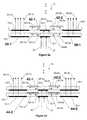
- FIGS. 1 a and 1 bare schematic representations of a virtual reality display (a cross sectional view shown in FIGS. 1 a ) having an exit pupil expander system with stacked diffractive exit pupil expanders (a cross sectional view is shown in FIG. 1 b );
- FIGS. 2 a and 2 bare schematic representations (cross-sectional views) demonstrating a color separation in an exit pupil expander system using absorbing tint through a volume of the substrates ( FIG. 1 a ) and through a thickness of selected areas of the substrates between in-coupling and out-coupling gratings, according to embodiments of the present invention;
- FIGS. 3 a and 3 bare schematic representations (cross-sectional views) demonstrating a color separation in an exit pupil expander system using absorbing tint spread throughout a resin in in-coupling and out-coupling gratings, according to embodiments of the present invention
- FIGS. 4 a and 4 bare schematic representations (cross-sectional views) demonstrating a color separation in an exit pupil expander system using absorbing tint spread throughout a resin in out-coupling gratings and absorbing coating across the in-coupling grating, according to embodiments of the present invention
- FIGS. 5 a and 5 bare schematic representations (cross-sectional views) demonstrating a color separation in an exit pupil expander system using absorbing coatings having substantially the same index of refraction as a substrate and disposed on the substrate in areas between in-coupling and out-coupling gratings, according to embodiments of the present invention.
- FIG. 6is a schematic representation of an electronic device, having an exit pupil expander system, according to an embodiment of the present invention.
- a new method and apparatusare presented for providing color separation in an exit pupil expander system that uses a plurality of diffractive elements for expanding the exit pupil of a display in an electronic device for viewing by introducing a selectively absorbing area or areas in the exit pupil expanders.
- the embodiments of the present inventioncan be applied to a broad optical spectral range of optical beams but most importantly to a visible part of the optical spectrum where the optical beams are called light beams.
- an optical devicee.g., the optical device can be a part of a virtual reality display
- Nbeing an integer of at least a value of one
- the gapcan be a material with a substantially smaller index of refraction than in the substrates, e.g., an air gap
- each such substratehaving a first surface and a second surface and acting as an exit pupil expander.
- Each substratecan comprise at least one diffractive element (e.g., a diffractive grating) disposed on the first or the second surface of said at least one substrate and which is configured to receive an input optical beam (i.e., at least one diffractive element acts as an in-coupling grating). It is noted that after propagating through the in-coupling grating of the first substrate, some “unselected” wavelength components of the input optical beam (i.e., a portion of the input optical beam) are received by the in-coupling grating of a second substrate in a stack of the N substrates and so on.
- a diffractive elemente.g., a diffractive grating
- each substratecan further comprise at least one further diffractive element (e.g., a diffractive grating) disposed on the first or the second surface and acting as an out-coupling grating.
- a further diffractive elemente.g., a diffractive grating
- itcan be two out-coupling gratings symmetrically located in the substrate to provide out-coupling for the left and for the right eye.
- each substratemay comprise at least one optically absorbing area or areas within or disposed on the substrate.
- the input optical beamcan be diffracted in the diffractive element (the in-coupling grating) to provide at least one (two in the biocular systems) diffracted optical beam substantially within the first and the second surfaces due to a total internal reflection, and then at least part of the at least one diffracted optical beam is further coupled out of each substrate by diffraction in the at least one further diffractive element (the out-coupling grating), thus providing an output optical beam (or two beams for the biocular systems) out of each substrate with an expanded exit pupil in one or two dimensions using wavelength selectivity as explained below.
- the input optical beamcan comprise K wavelength components (K being an integer of at least a value of two), such that the at least one optically absorbing area within or disposed on each of the substrates is configured to absorb M (M being an integer between 1 and K-1) pre-selected components of the K wavelength components and to propagate a selected component out of the K wavelength components, e.g., substantially without an optical intensity attenuation due to absorption. Then the output optical beam from each substrate substantially comprises the selected component out of the K wavelength components. It is noted that the diffraction gratings in each substrate are optimized (e.g., by choosing the appropriate period of the periodic lines) for the wavelength component to be selected by that grating.
- each of the N stacked substratesis configured to expand an exit pupil of substantially only one component out of said K wavelength components of the input optical beam such that all said K wavelength components merge together having substantially the same direction and location in an output of said optical device, therefore providing a color separation using the N exit pupil expanders that use a plurality of diffractive elements for expanding the exit pupil, e.g., of a display in the electronic device for viewing.
- Ncan be equal to K, i.e., each substrate only can output one wavelength (color) component.
- the optically absorbing area for any substrate out of the N substratescan be configured to absorb all K-1 wavelength components except only one selected wavelength components band to be provided in the output optical beam from that substrate.
- different substratescan be configured to absorb a different number of wavelength components depending on a specific system design.
- each substratein case of a two-dimensional exit pupil expansion, can comprise at least one intermediate diffractive element (two intermediate diffractive elements for the biocular case) such that the at least part of the input optical beam diffracted in the at least one diffractive element is first coupled to the at least one intermediate diffractive element, which then couples, using a further diffraction in the at least one intermediate diffractive element, the at least part of said diffracted optical beam to the at least one further diffractive element, which then provides a two-dimensional exit pupil expansion of said input optical beam.
- intermediate diffractive elementtwo intermediate diffractive elements for the biocular case
- the intermediate diffractive elementcan have an odd number of first order diffractions or an even number of further first order reflections as known in the art and, e.g., described by T. Levola in “Diffractive Optics for Virtual Reality Displays”, SID Eurodisplay 05, Edinburg (2005), SID 02 Digest, Paper 22.1.
- the at least one optically absorbing area within or disposed on each substratecan be configured using at least one approach or a combination thereof out of:
- each substratecan be configured to have an additional optically absorbing layer disposed on or adjacent to a surface of that substrate, wherein the surface being a second surface of that substrate through which the input optical beam propagates after being received by the substrate, such that the selected component out of the K wavelength components selected by that substrate is substantially absorbed in the additional optically absorbing layer, thus preventing said selected wavelength component from entering the next substrate.
- One practical example for implementing embodiments of the present inventioncan be a color separation for an RGB (red, green, blue) gamut.
- the first substrate in the stackcan “select” a short blue wavelength component and “absorb” the green and red
- the second substratecan “select” a green component
- the blue and red
- the third substrate in the stackcan “select” a long red wavelength component and “absorb” the green and blue. More implementation examples are provided in FIGS. 2 through 6 , according to various embodiments of the present invention.
- FIGS. 1 a and 1 bshow schematic representations of a virtual reality display (a cross sectional view shown in FIGS. 1 a ) having an exit pupil expander system 10 a with stacked diffractive exit pupil expanders 10 - 1 , 10 - 2 , etc. as shown in a cross sectional view in Figure lb with in-coupling gratings 12 - 1 and 12 - 2 , etc. and out-coupling gratings 14 - 1 , 14 - 2 , 16 - 1 and 16 - 2 for the biocular case.
- the input optical beamhas two wavelength components 20 ( ⁇ 1 ) and 22 ( ⁇ 2 ).
- ⁇ 1the input optical beam
- both components 20 and 22are coupled (see corresponding optical beams 20 - 1 a , 22 - 1 a , 20 - 2 a , 22 - 2 a , and unwanted optical beams 20 - 1 c , 22 - 1 c , 20 - 2 c , 22 - 2 c , respectively) to the corresponding out-coupling gratings 14 - 1 , 14 - 2 , 16 - 1 and 16 - 2 in each of the substrates 10 - 1 and 10 - 2 as shown in FIG.
- FIGS. 2 a and 2 bshow examples among others of schematic representations (cross-sectional views) demonstrating a color separation in an exit pupil expander system 10 using absorbing tint through a volume of the substrates 10 - 1 and 10 - 2 ( FIG. 1 a ) and through a thickness of selected areas 10 - 1 a , 10 - 2 a , 10 - 1 b and 10 - 2 b of the substrates 10 - 1 and 10 - 2 between the in-coupling gratings 12 - 1 and 12 - 2 , and the out-coupling gratings 14 - 1 , 14 - 2 , 16 - 1 and 16 - 2 , respectively, as shown in FIG.
- each of the substrates 10 - 1 and 10 - 2provides only one wavelength component: the optical beams 20 - 1 b and 20 - 2 b representing the wavelength component 20 are provided by the substrate 10 - 1 , and the optical beams 22 - 1 b and 22 - 2 b representing the wavelength component 22 are provided by the substrate 10 - 2 , respectively.
- FIGS. 3 a and 3 bshow examples among others of schematic representations (cross-sectional views) of a color separation in an exit pupil expander system 10 using the absorbing tint spread throughout a resin used in the in-coupling gratings 12 - 1 and 12 - 2 and/or in the out-coupling gratings 34 - 1 , 34 - 2 , 36 - 1 and 36 - 2 , according to embodiments of the present invention.
- FIG. 3 a and 3 bshow examples among others of schematic representations (cross-sectional views) of a color separation in an exit pupil expander system 10 using the absorbing tint spread throughout a resin used in the in-coupling gratings 12 - 1 and 12 - 2 and/or in the out-coupling gratings 34 - 1 , 34 - 2 , 36 - 1 and 36 - 2 , according to embodiments of the present invention.
- FIG. 3 a and 3 bshow examples among others of schematic representations (cross-sectional views) of
- the absorbing tint in the diffraction gratings 34 - 1 , 36 - 1 of the first substrate 10 - 1is optimized for absorbing the wavelength component 22 while being transparent to the wavelength component 20
- the absorbing tint in the diffraction gratings 34 - 2 , 36 - 2 of the first substrate 10 - 2is optimized for absorbing the wavelength component 20 while being transparent to the wavelength component 22 , thus eliminating unwanted optical beams 20 - 1 c , 22 - 1 c , 20 - 2 c , 22 - 2 c by absorption in the out-coupling gratings 34 - 1 , 34 - 2 , 36 - 1 and 36 - 2 .
- the in-coupling grating 12 - 2provides an initial attenuation of the unwanted optical beams 20 - 1 c and 20 - 2 c as shown in FIG. 3 a . If the in-coupling grating 12 - 2 can provide enough attenuation of the unwanted optical beams 20 - 1 c and 20 - 2 c , then the out-couplings 14 - 2 and 16 - 2 do not need to be tinted at all as shown in FIG. 3 b .
- FIG. 4 ashows an example among others of schematic representations (cross-sectional views) demonstrating a color separation in an exit pupil expander system 10 using the absorbing tint spread throughout a resin in the out-coupling gratings 34 - 1 , 34 - 2 , 36 - 1 and 36 - 2 such that the unwanted optical beams 20 - 1 c , 22 - 1 c , 20 - 2 c , 22 - 2 c are eliminated by absorption in the out-coupling gratings 34 - 1 , 34 - 2 , 36 - 1 and 36 - 2 , respectively.
- an optically absorbing layer 40 disposed on or adjacent to a surface of the substrate 10 - 1 across the in-coupling grating 12 - 1can absorb the wavelength component 20 for minimizing the presence of the unwanted optical beams 20 - 1 c and 20 - 2 c . If the in-coupling grating 12 - 2 can provide enough attenuation of the unwanted optical beams 20 - 1 c and 20 - 2 c , then the out-couplings 14 - 2 and 16 - 2 do not need to be tinted at all as shown in FIG. 4 b .
- FIG. 5 ashows an example among others of schematic representations (cross-sectional views) demonstrating a color separation in an exit pupil expander system 10 using the absorbing tint spread throughout the resin in the out-coupling gratings 34 - 1 and 36 - 1 of the first substrate 10 - 1 such that the unwanted optical beams 22 - 1 c and 22 - 2 c are eliminated by absorption in the out-coupling gratings 34 - 1 and 36 - 1 , respectively.
- absorbing coatings 42 - 1 and 42 - 2having substantially the same index of refraction as the substrate 10 - 2 and disposed on the substrate 10 - 2 in areas between the in-coupling grating 12 - 2 and the out-coupling gratings 14 - 2 and 16 - 2 , respectively, according to an embodiment of the present invention.
- These absorbing coatings 42 - 1 and 42 - 2substantially absorb the unwanted optical beams 20 - 1 c and 20 - 2 c in the second substrate 10 - 2 acting as a boundary for the total internal reflection.
- FIG. 5 binstead of using the absorbing tint spread throughout the resin in the out-coupling gratings (as shown in FIG.
- tintingis a known art, e.g., see U.S. Pat. No. 6,464,733 “Tinting plastic articles” by C. U. Ryser.
- the parts that needs to be tintedcan be tinted separately. Then these parts can be molded together with clear plastics.
- the tinted and not tinted partsshould have the same refractive index, which is usually the case, if the same material is used thoroughly, because the tinting does not usually alter the refractive index.
- radiation methodsmay be used for creating color centers in the material to alter the spectral absorption.
- the diffraction gratingscan be formed using a UV (ultraviolet) curable resin, which is tinted which, as known in the art.
- FIG. 6shows an example of a schematic representation of an electronic device, having the exit pupil expander (EPE) system 10 , according to an embodiment of the present invention.
- EPEexit pupil expander
- the exit pupil expander (EPE) 10 , 10 a or 10 bcan be used in an electronic (portable) device 100 , such as a mobile phone, personal digital assistant (PDA), communicator, portable Internet appliance, hand-hand computer, digital video and still camera, wearable computer, computer game device, specialized bring-to-the-eye product for viewing and other portable electronic devices.
- the portable device 100has a housing 210 to house a communication unit 212 for receiving and transmitting information from and to an external device (not shown).
- the portable device 100also has a controlling and processing unit 214 for handling the received and transmitted information, and a virtual display system 230 for viewing.
- the virtual display system 230includes a micro-display or an image source 192 and an optical engine 190 .
- the controlling and processing unit 214is operatively connected to the optical engine 190 to provide image data to the image source 192 to display an image thereon.
- the EPE 10can be optically linked to an optical engine 190 .
- the image source 192can be a sequential color LCOS (Liquid Crystal On Silicon) device, an OLED (Organic Light Emitting Diode) array, an MEMS (MicroElectro Mechanical System) device or any other suitable micro-display device operating in transmission, reflection or emission.
- LCOSLiquid Crystal On Silicon
- OLEDOrganic Light Emitting Diode
- MEMSMicroElectro Mechanical System
- the electronic device 100can be a portable device, such as a mobile phone, personal digital assistant (PDA), communicator, portable Internet appliance, hand-held computer, digital video and still camera, wearable computer, computer game device, specialized bring-to-the-eye product for viewing and other portable electronic devices.
- PDApersonal digital assistant
- the exit pupil expandercan also be used in a non-portable device, such as a gaming device, vending machine, band-o-matic, and home appliances, such as an oven, microwave oven and other appliances and other non-portable devices.
Landscapes
- Physics & Mathematics (AREA)
- General Physics & Mathematics (AREA)
- Optics & Photonics (AREA)
- Diffracting Gratings Or Hologram Optical Elements (AREA)
- Liquid Crystal (AREA)
- Devices For Indicating Variable Information By Combining Individual Elements (AREA)
Abstract
Description
- a data processing unit;
- an optical engine operatively connected to the data processing unit for receiving image data from the data processing unit;
- a display device operatively connected to the optical engine for forming an image based on the image data; and
- an exit pupil expander comprising:
- at least one substrate of optical material having a first surface and a second surface;
- at least one diffractive element disposed on the first or the second surface of the at least one substrate and configured to receive an input optical beam;
- at least one further diffractive element disposed on the first or the second surface; and
- at least one optically absorbing area within or disposed on the at least one substrate, wherein
- at least part of the input optical beam is diffracted in the diffractive element to provide at least one diffracted optical beam substantially within the first and the second surfaces, and
- at least part of the at least one diffracted optical beam is coupled out of the at least one substrate by diffraction in the at least one further diffractive element, thus providing an output optical beam out of the at least one substrate with an expanded exit pupil in one or two dimensions, wherein
- the input optical beam comprises K wavelength components and the at least one optically absorbing area is configured to absorb M pre-selected components out of the K wavelength components and to propagate a selected component out of the K wavelength components substantially without an optical intensity attenuation, such that the output optical beam comprises the selected component out of the K wavelength components, wherein K is an integer of at least a value of two and M is an integer between 1 and K-1.
- for receiving an input optical beam by at least one means for diffraction disposed on a first or a second surface of at least one substrate, the input optical beam comprises K wavelength components, wherein K is an integer of at least a value of two, and
- for diffracting at least part of the input optical beam in the at least one means for diffraction to provide at least one diffracted optical beam substantially within the first and second surfaces;
- a) an absorbing tint spread throughout a volume of each substrate,
- b) an absorbing tint spread throughout a thickness of each substrate only in areas of each substrate between the at least one diffractive element and at least one further diffractive element (i.e., between the in-coupling and the out-coupling diffraction gratings),
- c) an absorbing tint spread throughout a resin used to make the at least one diffractive element, the at least one further diffractive element, and/or the intermediate grating,
- d) an absorbing coating, having substantially the same index of refraction as each substrate, disposed on each substrate in an area substantially between the at least one diffractive element and at least one further diffractive element (i.e., between the in-coupling and the out-coupling diffraction gratings), etc.
Claims (22)
Applications Claiming Priority (1)
| Application Number | Priority Date | Filing Date | Title |
|---|---|---|---|
| PCT/IB2006/001450WO2007141587A1 (en) | 2006-06-02 | 2006-06-02 | Color distribution in exit pupil expanders |
Related Parent Applications (1)
| Application Number | Title | Priority Date | Filing Date |
|---|---|---|---|
| PCT/IB2006/001450A-371-Of-InternationalWO2007141587A1 (en) | 2006-06-02 | 2006-06-02 | Color distribution in exit pupil expanders |
Related Child Applications (1)
| Application Number | Title | Priority Date | Filing Date |
|---|---|---|---|
| US13/594,060ContinuationUS8547638B2 (en) | 2006-06-02 | 2012-08-24 | Color distribution in exit pupil expanders |
Publications (2)
| Publication Number | Publication Date |
|---|---|
| US20100165465A1 US20100165465A1 (en) | 2010-07-01 |
| US8254031B2true US8254031B2 (en) | 2012-08-28 |
Family
ID=38801095
Family Applications (2)
| Application Number | Title | Priority Date | Filing Date |
|---|---|---|---|
| US12/227,738Active2028-01-19US8254031B2 (en) | 2006-06-02 | 2006-06-02 | Color distribution in exit pupil expanders |
| US13/594,060ActiveUS8547638B2 (en) | 2006-06-02 | 2012-08-24 | Color distribution in exit pupil expanders |
Family Applications After (1)
| Application Number | Title | Priority Date | Filing Date |
|---|---|---|---|
| US13/594,060ActiveUS8547638B2 (en) | 2006-06-02 | 2012-08-24 | Color distribution in exit pupil expanders |
Country Status (6)
| Country | Link |
|---|---|
| US (2) | US8254031B2 (en) |
| EP (1) | EP2035881B8 (en) |
| JP (1) | JP2009539128A (en) |
| CN (1) | CN101460882B (en) |
| TW (1) | TWI348032B (en) |
| WO (1) | WO2007141587A1 (en) |
Cited By (70)
| Publication number | Priority date | Publication date | Assignee | Title |
|---|---|---|---|---|
| US20140140653A1 (en)* | 2012-11-16 | 2014-05-22 | Rockwell Collins, Inc. | Transparent waveguide display |
| US20150138248A1 (en)* | 2012-05-03 | 2015-05-21 | Martin Schrader | Image Providing Apparatus, Method and Computer Program |
| US9086568B2 (en) | 2013-04-18 | 2015-07-21 | Nokia Technologies Oy | Method and apparatus for view recovery |
| WO2016179246A1 (en)* | 2015-05-04 | 2016-11-10 | Magic Leap, Inc. | Separated pupil optical systems for virtual and augmented reality and methods for displaying images using same |
| US9507150B1 (en) | 2011-09-30 | 2016-11-29 | Rockwell Collins, Inc. | Head up display (HUD) using a bent waveguide assembly |
| US9519089B1 (en) | 2014-01-30 | 2016-12-13 | Rockwell Collins, Inc. | High performance volume phase gratings |
| US9523852B1 (en) | 2012-03-28 | 2016-12-20 | Rockwell Collins, Inc. | Micro collimator system and method for a head up display (HUD) |
| US9674413B1 (en) | 2013-04-17 | 2017-06-06 | Rockwell Collins, Inc. | Vision system and method having improved performance and solar mitigation |
| US9715067B1 (en) | 2011-09-30 | 2017-07-25 | Rockwell Collins, Inc. | Ultra-compact HUD utilizing waveguide pupil expander with surface relief gratings in high refractive index materials |
| US9766465B1 (en) | 2014-03-25 | 2017-09-19 | Rockwell Collins, Inc. | Near eye display system and method for display enhancement or redundancy |
| US9933684B2 (en) | 2012-11-16 | 2018-04-03 | Rockwell Collins, Inc. | Transparent waveguide display providing upper and lower fields of view having a specific light output aperture configuration |
| US9977247B1 (en) | 2011-09-30 | 2018-05-22 | Rockwell Collins, Inc. | System for and method of displaying information without need for a combiner alignment detector |
| US10088675B1 (en) | 2015-05-18 | 2018-10-02 | Rockwell Collins, Inc. | Turning light pipe for a pupil expansion system and method |
| US10108010B2 (en) | 2015-06-29 | 2018-10-23 | Rockwell Collins, Inc. | System for and method of integrating head up displays and head down displays |
| US10126552B2 (en) | 2015-05-18 | 2018-11-13 | Rockwell Collins, Inc. | Micro collimator system and method for a head up display (HUD) |
| US10156681B2 (en) | 2015-02-12 | 2018-12-18 | Digilens Inc. | Waveguide grating device |
| US10241330B2 (en) | 2014-09-19 | 2019-03-26 | Digilens, Inc. | Method and apparatus for generating input images for holographic waveguide displays |
| US10247943B1 (en) | 2015-05-18 | 2019-04-02 | Rockwell Collins, Inc. | Head up display (HUD) using a light pipe |
| US10295824B2 (en) | 2017-01-26 | 2019-05-21 | Rockwell Collins, Inc. | Head up display with an angled light pipe |
| US10359736B2 (en) | 2014-08-08 | 2019-07-23 | Digilens Inc. | Method for holographic mastering and replication |
| US10509241B1 (en) | 2009-09-30 | 2019-12-17 | Rockwell Collins, Inc. | Optical displays |
| US10545346B2 (en) | 2017-01-05 | 2020-01-28 | Digilens Inc. | Wearable heads up displays |
| US10598932B1 (en) | 2016-01-06 | 2020-03-24 | Rockwell Collins, Inc. | Head up display for integrating views of conformally mapped symbols and a fixed image source |
| US10642058B2 (en) | 2011-08-24 | 2020-05-05 | Digilens Inc. | Wearable data display |
| US10670876B2 (en) | 2011-08-24 | 2020-06-02 | Digilens Inc. | Waveguide laser illuminator incorporating a despeckler |
| US10678053B2 (en) | 2009-04-27 | 2020-06-09 | Digilens Inc. | Diffractive projection apparatus |
| US10690916B2 (en) | 2015-10-05 | 2020-06-23 | Digilens Inc. | Apparatus for providing waveguide displays with two-dimensional pupil expansion |
| US10690915B2 (en) | 2012-04-25 | 2020-06-23 | Rockwell Collins, Inc. | Holographic wide angle display |
| US10725312B2 (en) | 2007-07-26 | 2020-07-28 | Digilens Inc. | Laser illumination device |
| US10732569B2 (en) | 2018-01-08 | 2020-08-04 | Digilens Inc. | Systems and methods for high-throughput recording of holographic gratings in waveguide cells |
| US10732407B1 (en) | 2014-01-10 | 2020-08-04 | Rockwell Collins, Inc. | Near eye head up display system and method with fixed combiner |
| US10747982B2 (en) | 2013-07-31 | 2020-08-18 | Digilens Inc. | Method and apparatus for contact image sensing |
| US10795160B1 (en) | 2014-09-25 | 2020-10-06 | Rockwell Collins, Inc. | Systems for and methods of using fold gratings for dual axis expansion |
| US10815145B2 (en) | 2016-03-31 | 2020-10-27 | Corning Incorporated | High index glass and devices incorporating such |
| US10859768B2 (en) | 2016-03-24 | 2020-12-08 | Digilens Inc. | Method and apparatus for providing a polarization selective holographic waveguide device |
| US10890707B2 (en) | 2016-04-11 | 2021-01-12 | Digilens Inc. | Holographic waveguide apparatus for structured light projection |
| US10914950B2 (en) | 2018-01-08 | 2021-02-09 | Digilens Inc. | Waveguide architectures and related methods of manufacturing |
| US10942430B2 (en) | 2017-10-16 | 2021-03-09 | Digilens Inc. | Systems and methods for multiplying the image resolution of a pixelated display |
| US20210231951A1 (en)* | 2018-07-23 | 2021-07-29 | Magic Leap, Inc. | Systems and methods for external light management |
| US11103763B2 (en) | 2018-09-11 | 2021-08-31 | Real Shot Inc. | Basketball shooting game using smart glasses |
| US11141645B2 (en) | 2018-09-11 | 2021-10-12 | Real Shot Inc. | Athletic ball game using smart glasses |
| US11204462B2 (en) | 2017-01-23 | 2021-12-21 | Magic Leap, Inc. | Eyepiece for virtual, augmented, or mixed reality systems |
| US11237393B2 (en) | 2018-11-20 | 2022-02-01 | Magic Leap, Inc. | Eyepieces for augmented reality display system |
| US11256155B2 (en) | 2012-01-06 | 2022-02-22 | Digilens Inc. | Contact image sensor using switchable Bragg gratings |
| US11300795B1 (en) | 2009-09-30 | 2022-04-12 | Digilens Inc. | Systems for and methods of using fold gratings coordinated with output couplers for dual axis expansion |
| US11307432B2 (en) | 2014-08-08 | 2022-04-19 | Digilens Inc. | Waveguide laser illuminator incorporating a Despeckler |
| US11314084B1 (en) | 2011-09-30 | 2022-04-26 | Rockwell Collins, Inc. | Waveguide combiner system and method with less susceptibility to glare |
| US11347063B2 (en) | 2017-12-15 | 2022-05-31 | Magic Leap, Inc. | Eyepieces for augmented reality display system |
| US11366316B2 (en) | 2015-05-18 | 2022-06-21 | Rockwell Collins, Inc. | Head up display (HUD) using a light pipe |
| US11378732B2 (en) | 2019-03-12 | 2022-07-05 | DigLens Inc. | Holographic waveguide backlight and related methods of manufacturing |
| US11378864B2 (en)* | 2016-11-18 | 2022-07-05 | Magic Leap, Inc. | Waveguide light multiplexer using crossed gratings |
| US11402629B2 (en) | 2013-11-27 | 2022-08-02 | Magic Leap, Inc. | Separated pupil optical systems for virtual and augmented reality and methods for displaying images using same |
| US11402801B2 (en) | 2018-07-25 | 2022-08-02 | Digilens Inc. | Systems and methods for fabricating a multilayer optical structure |
| US11442222B2 (en) | 2019-08-29 | 2022-09-13 | Digilens Inc. | Evacuated gratings and methods of manufacturing |
| US11487131B2 (en) | 2011-04-07 | 2022-11-01 | Digilens Inc. | Laser despeckler based on angular diversity |
| US11513350B2 (en) | 2016-12-02 | 2022-11-29 | Digilens Inc. | Waveguide device with uniform output illumination |
| US11543594B2 (en) | 2019-02-15 | 2023-01-03 | Digilens Inc. | Methods and apparatuses for providing a holographic waveguide display using integrated gratings |
| US11650423B2 (en) | 2019-06-20 | 2023-05-16 | Magic Leap, Inc. | Eyepieces for augmented reality display system |
| US11681143B2 (en) | 2019-07-29 | 2023-06-20 | Digilens Inc. | Methods and apparatus for multiplying the image resolution and field-of-view of a pixelated display |
| US11726332B2 (en) | 2009-04-27 | 2023-08-15 | Digilens Inc. | Diffractive projection apparatus |
| US11726329B2 (en) | 2015-01-12 | 2023-08-15 | Digilens Inc. | Environmentally isolated waveguide display |
| US11747568B2 (en) | 2019-06-07 | 2023-09-05 | Digilens Inc. | Waveguides incorporating transmissive and reflective gratings and related methods of manufacturing |
| US12092914B2 (en) | 2018-01-08 | 2024-09-17 | Digilens Inc. | Systems and methods for manufacturing waveguide cells |
| US12140764B2 (en) | 2019-02-15 | 2024-11-12 | Digilens Inc. | Wide angle waveguide display |
| US12158612B2 (en) | 2021-03-05 | 2024-12-03 | Digilens Inc. | Evacuated periodic structures and methods of manufacturing |
| US12210153B2 (en) | 2019-01-14 | 2025-01-28 | Digilens Inc. | Holographic waveguide display with light control layer |
| US12306585B2 (en) | 2018-01-08 | 2025-05-20 | Digilens Inc. | Methods for fabricating optical waveguides |
| US12379599B2 (en) | 2021-05-19 | 2025-08-05 | Huawei Technologies Co., Ltd. | Light guide and near-eye display apparatus |
| US12397477B2 (en) | 2019-02-05 | 2025-08-26 | Digilens Inc. | Methods for compensating for optical surface nonuniformity |
| US12399326B2 (en) | 2021-01-07 | 2025-08-26 | Digilens Inc. | Grating structures for color waveguides |
Families Citing this family (70)
| Publication number | Priority date | Publication date | Assignee | Title |
|---|---|---|---|---|
| GB0522968D0 (en) | 2005-11-11 | 2005-12-21 | Popovich Milan M | Holographic illumination device |
| EP2229603B1 (en) | 2007-12-17 | 2012-08-29 | Nokia Corporation | Exit pupil expanders with spherical and aspheric substrates |
| WO2009077802A1 (en)* | 2007-12-18 | 2009-06-25 | Nokia Corporation | Exit pupil expanders with wide field-of-view |
| US20200057353A1 (en) | 2009-10-09 | 2020-02-20 | Digilens Inc. | Compact Edge Illuminated Diffractive Display |
| US11204540B2 (en) | 2009-10-09 | 2021-12-21 | Digilens Inc. | Diffractive waveguide providing a retinal image |
| US8659826B1 (en) | 2010-02-04 | 2014-02-25 | Rockwell Collins, Inc. | Worn display system and method without requiring real time tracking for boresight precision |
| US9766381B2 (en) | 2010-03-12 | 2017-09-19 | Nokia Technologies Oy | Light-guiding structures |
| WO2011131978A1 (en)* | 2010-04-23 | 2011-10-27 | Bae Systems Plc | Optical waveguide and display device |
| EP2381290A1 (en)* | 2010-04-23 | 2011-10-26 | BAE Systems PLC | Optical waveguide and display device |
| GB201114149D0 (en) | 2011-08-17 | 2011-10-05 | Bae Systems Plc | Projection display |
| WO2013167864A1 (en) | 2012-05-11 | 2013-11-14 | Milan Momcilo Popovich | Apparatus for eye tracking |
| US8885997B2 (en)* | 2012-08-31 | 2014-11-11 | Microsoft Corporation | NED polarization system for wavelength pass-through |
| US10209517B2 (en) | 2013-05-20 | 2019-02-19 | Digilens, Inc. | Holographic waveguide eye tracker |
| US9244281B1 (en) | 2013-09-26 | 2016-01-26 | Rockwell Collins, Inc. | Display system and method using a detached combiner |
| US9529196B1 (en) | 2014-06-05 | 2016-12-27 | Iphysicist Ltd. | Image guide optics for near eye displays |
| US9715110B1 (en) | 2014-09-25 | 2017-07-25 | Rockwell Collins, Inc. | Automotive head up display (HUD) |
| EP3198192A1 (en) | 2014-09-26 | 2017-08-02 | Milan Momcilo Popovich | Holographic waveguide opticaltracker |
| US20180275402A1 (en) | 2015-01-12 | 2018-09-27 | Digilens, Inc. | Holographic waveguide light field displays |
| EP3248026B1 (en) | 2015-01-20 | 2019-09-04 | DigiLens Inc. | Holographic waveguide lidar |
| EP3062142B1 (en) | 2015-02-26 | 2018-10-03 | Nokia Technologies OY | Apparatus for a near-eye display |
| WO2016146963A1 (en) | 2015-03-16 | 2016-09-22 | Popovich, Milan, Momcilo | Waveguide device incorporating a light pipe |
| WO2016156776A1 (en) | 2015-03-31 | 2016-10-06 | Milan Momcilo Popovich | Method and apparatus for contact image sensing |
| US10670862B2 (en) | 2015-07-02 | 2020-06-02 | Microsoft Technology Licensing, Llc | Diffractive optical elements with asymmetric profiles |
| US10038840B2 (en)* | 2015-07-30 | 2018-07-31 | Microsoft Technology Licensing, Llc | Diffractive optical element using crossed grating for pupil expansion |
| US10073278B2 (en) | 2015-08-27 | 2018-09-11 | Microsoft Technology Licensing, Llc | Diffractive optical element using polarization rotation grating for in-coupling |
| US10429645B2 (en) | 2015-10-07 | 2019-10-01 | Microsoft Technology Licensing, Llc | Diffractive optical element with integrated in-coupling, exit pupil expansion, and out-coupling |
| US10241332B2 (en) | 2015-10-08 | 2019-03-26 | Microsoft Technology Licensing, Llc | Reducing stray light transmission in near eye display using resonant grating filter |
| JP6597197B2 (en)* | 2015-11-05 | 2019-10-30 | セイコーエプソン株式会社 | Beam diameter expanding element and display device |
| US10234686B2 (en) | 2015-11-16 | 2019-03-19 | Microsoft Technology Licensing, Llc | Rainbow removal in near-eye display using polarization-sensitive grating |
| CN109073889B (en) | 2016-02-04 | 2021-04-27 | 迪吉伦斯公司 | Holographic waveguide optical tracker |
| JP6736911B2 (en)* | 2016-02-29 | 2020-08-05 | セイコーエプソン株式会社 | Luminous flux diameter expanding element and image display device |
| US9791703B1 (en) | 2016-04-13 | 2017-10-17 | Microsoft Technology Licensing, Llc | Waveguides with extended field of view |
| US10067347B2 (en) | 2016-04-13 | 2018-09-04 | Microsoft Technology Licensing, Llc | Waveguides with improved intensity distributions |
| AU2017264780B2 (en)* | 2016-05-12 | 2022-05-12 | Magic Leap, Inc. | Distributed light manipulation over imaging waveguide |
| US10353202B2 (en)* | 2016-06-09 | 2019-07-16 | Microsoft Technology Licensing, Llc | Wrapped waveguide with large field of view |
| US10095045B2 (en) | 2016-09-12 | 2018-10-09 | Microsoft Technology Licensing, Llc | Waveguide comprising a bragg polarization grating |
| US10371896B2 (en)* | 2016-12-22 | 2019-08-06 | Magic Leap, Inc. | Color separation in planar waveguides using dichroic filters |
| US10650552B2 (en) | 2016-12-29 | 2020-05-12 | Magic Leap, Inc. | Systems and methods for augmented reality |
| EP4300160A3 (en) | 2016-12-30 | 2024-05-29 | Magic Leap, Inc. | Polychromatic light out-coupling apparatus, near-eye displays comprising the same, and method of out-coupling polychromatic light |
| CN110300912B (en)* | 2017-02-15 | 2022-09-02 | 奇跃公司 | Projector architecture including artifact mitigation |
| US10838110B2 (en)* | 2017-03-03 | 2020-11-17 | Microsoft Technology Licensing, Llc | Metasurface optical coupling elements for a display waveguide |
| KR102375975B1 (en)* | 2017-04-28 | 2022-03-17 | 삼성디스플레이 주식회사 | Display device, organic light emitting display device and head mount display device |
| US10578870B2 (en) | 2017-07-26 | 2020-03-03 | Magic Leap, Inc. | Exit pupil expander |
| KR102858869B1 (en) | 2017-12-10 | 2025-09-11 | 매직 립, 인코포레이티드 | Anti-reflective coatings on optical waveguides |
| CN111712751B (en) | 2017-12-20 | 2022-11-01 | 奇跃公司 | Insert for augmented reality viewing apparatus |
| US10755676B2 (en) | 2018-03-15 | 2020-08-25 | Magic Leap, Inc. | Image correction due to deformation of components of a viewing device |
| US10690851B2 (en) | 2018-03-16 | 2020-06-23 | Digilens Inc. | Holographic waveguides incorporating birefringence control and methods for their fabrication |
| FI130178B (en) | 2018-03-28 | 2023-03-29 | Dispelix Oy | Waveguide element and waveguide stack for display applications |
| US11204491B2 (en) | 2018-05-30 | 2021-12-21 | Magic Leap, Inc. | Compact variable focus configurations |
| JP7319303B2 (en) | 2018-05-31 | 2023-08-01 | マジック リープ, インコーポレイテッド | Radar head pose localization |
| US10825424B2 (en) | 2018-06-05 | 2020-11-03 | Magic Leap, Inc. | Homography transformation matrices based temperature calibration of a viewing system |
| US11579441B2 (en) | 2018-07-02 | 2023-02-14 | Magic Leap, Inc. | Pixel intensity modulation using modifying gain values |
| WO2020010226A1 (en) | 2018-07-03 | 2020-01-09 | Magic Leap, Inc. | Systems and methods for virtual and augmented reality |
| US11856479B2 (en) | 2018-07-03 | 2023-12-26 | Magic Leap, Inc. | Systems and methods for virtual and augmented reality along a route with markers |
| CN112585581B (en) | 2018-07-10 | 2024-10-18 | 奇跃公司 | Thread weaving for cross-ISA procedure calls |
| CN119197613A (en) | 2018-07-24 | 2024-12-27 | 奇跃公司 | Temperature-dependent calibration of mobile detection equipment |
| WO2020023543A1 (en) | 2018-07-24 | 2020-01-30 | Magic Leap, Inc. | Viewing device with dust seal integration |
| WO2020028834A1 (en) | 2018-08-02 | 2020-02-06 | Magic Leap, Inc. | A viewing system with interpupillary distance compensation based on head motion |
| CN116820239A (en) | 2018-08-03 | 2023-09-29 | 奇跃公司 | Fusion gesture based drift correction of fusion gestures for totem in a user interaction system |
| WO2020041615A1 (en) | 2018-08-22 | 2020-02-27 | Magic Leap, Inc. | Patient viewing system |
| EP3881279A4 (en) | 2018-11-16 | 2022-08-17 | Magic Leap, Inc. | Image size triggered clarification to maintain image sharpness |
| CN118409394A (en) | 2018-12-21 | 2024-07-30 | 奇跃公司 | Cavitation structures for promoting total internal reflection in waveguides |
| WO2020163603A1 (en) | 2019-02-06 | 2020-08-13 | Magic Leap, Inc. | Target intent-based clock speed determination and adjustment to limit total heat generated by multiple processors |
| JP2022523852A (en) | 2019-03-12 | 2022-04-26 | マジック リープ, インコーポレイテッド | Aligning local content between first and second augmented reality viewers |
| WO2020223636A1 (en) | 2019-05-01 | 2020-11-05 | Magic Leap, Inc. | Content provisioning system and method |
| WO2021021670A1 (en) | 2019-07-26 | 2021-02-04 | Magic Leap, Inc. | Systems and methods for augmented reality |
| US20210055551A1 (en)* | 2019-08-23 | 2021-02-25 | Facebook Technologies, Llc | Dispersion compensation in volume bragg grating-based waveguide display |
| JP7635230B2 (en) | 2019-11-14 | 2025-02-25 | マジック リープ, インコーポレイテッド | Systems and methods for virtual and augmented reality |
| CN114667538A (en) | 2019-11-15 | 2022-06-24 | 奇跃公司 | Viewing system for use in a surgical environment |
| JP2024502255A (en) | 2020-12-21 | 2024-01-18 | ディジレンズ インコーポレイテッド | Eye glow suppression in waveguide-based displays |
Citations (11)
| Publication number | Priority date | Publication date | Assignee | Title |
|---|---|---|---|---|
| JPS5714806A (en) | 1980-07-01 | 1982-01-26 | Takumi Tomijima | Wavelength multiplex optical transmitting and receiving distributor |
| WO1999052002A1 (en) | 1998-04-02 | 1999-10-14 | Elop Electro-Optics Industries Ltd. | Holographic optical devices |
| US6117923A (en) | 1997-04-22 | 2000-09-12 | Mitsubishi Gas Chemical Company, Inc. | Resin for optical material |
| US6464733B2 (en) | 1998-09-03 | 2002-10-15 | Christophe U. Ryser | Tinting plastic articles |
| WO2003032017A2 (en) | 2001-10-09 | 2003-04-17 | Planop Planar Optics Ltd. | Optical device |
| WO2004034106A1 (en) | 2002-10-11 | 2004-04-22 | Koninklijke Philips Electronics N.V. | Light-transmitting substrate provided with a light-absorbing coating |
| WO2004055556A1 (en) | 2002-12-16 | 2004-07-01 | Nokia Corporation | Diffractive grating element for balancing diffraction efficiency |
| US6805490B2 (en) | 2002-09-30 | 2004-10-19 | Nokia Corporation | Method and system for beam expansion in a display device |
| US20040233534A1 (en) | 1999-06-16 | 2004-11-25 | Hideyuki Nakanishi | Diffractive optical element that polarizes light and an optical pickup using the same |
| WO2004109349A2 (en) | 2003-06-10 | 2004-12-16 | Elop Electro-Optics Industries Ltd. | Method and system for displaying an informative image against a background image |
| US7206107B2 (en) | 2004-12-13 | 2007-04-17 | Nokia Corporation | Method and system for beam expansion in a display device |
Family Cites Families (14)
| Publication number | Priority date | Publication date | Assignee | Title |
|---|---|---|---|---|
| US5224198A (en)* | 1991-09-30 | 1993-06-29 | Motorola, Inc. | Waveguide virtual image display |
| DE69432526T2 (en)* | 1993-02-26 | 2004-04-01 | Yeda Research And Development Co., Ltd. | OPTICAL HOLOGRAPHIC DEVICES |
| JP4048889B2 (en) | 2001-09-27 | 2008-02-20 | 旭硝子株式会社 | Driving method of liquid crystal display device |
| JP4039045B2 (en)* | 2001-11-26 | 2008-01-30 | コニカミノルタホールディングス株式会社 | BANDPASS FILTER AND VIDEO DISPLAY DEVICE |
| CN1432841A (en)* | 2002-01-16 | 2003-07-30 | 深圳市东方景电子有限公司 | Optical system with high image quality for head display |
| JP3946062B2 (en)* | 2002-03-18 | 2007-07-18 | シャープ株式会社 | Display device and manufacturing method thereof |
| KR20030088218A (en)* | 2002-05-13 | 2003-11-19 | 삼성전자주식회사 | Wearable color-display system |
| JP2004012768A (en)* | 2002-06-06 | 2004-01-15 | Nikon Corp | Combiner optics |
| JP2004077771A (en) | 2002-08-16 | 2004-03-11 | Fujitsu Ltd | Diffraction grating mask |
| US7418170B2 (en)* | 2004-03-29 | 2008-08-26 | Sony Corporation | Optical device and virtual image display device |
| JP4412059B2 (en) | 2004-06-02 | 2010-02-10 | セイコーエプソン株式会社 | Organic EL devices, electronic devices |
| US7807488B2 (en) | 2004-09-27 | 2010-10-05 | Qualcomm Mems Technologies, Inc. | Display element having filter material diffused in a substrate of the display element |
| JP2006162798A (en)* | 2004-12-03 | 2006-06-22 | Konica Minolta Photo Imaging Inc | Optical device, image display device, and head-mounted display |
| US7573640B2 (en)* | 2005-04-04 | 2009-08-11 | Mirage Innovations Ltd. | Multi-plane optical apparatus |
- 2006
- 2006-06-02CNCN2006800548132Apatent/CN101460882B/enactiveActive
- 2006-06-02WOPCT/IB2006/001450patent/WO2007141587A1/enactiveApplication Filing
- 2006-06-02JPJP2009512688Apatent/JP2009539128A/enactivePending
- 2006-06-02EPEP06755936.9Apatent/EP2035881B8/enactiveActive
- 2006-06-02USUS12/227,738patent/US8254031B2/enactiveActive
- 2007
- 2007-04-11TWTW096112694Apatent/TWI348032B/enactive
- 2012
- 2012-08-24USUS13/594,060patent/US8547638B2/enactiveActive
Patent Citations (12)
| Publication number | Priority date | Publication date | Assignee | Title |
|---|---|---|---|---|
| JPS5714806A (en) | 1980-07-01 | 1982-01-26 | Takumi Tomijima | Wavelength multiplex optical transmitting and receiving distributor |
| US6117923A (en) | 1997-04-22 | 2000-09-12 | Mitsubishi Gas Chemical Company, Inc. | Resin for optical material |
| WO1999052002A1 (en) | 1998-04-02 | 1999-10-14 | Elop Electro-Optics Industries Ltd. | Holographic optical devices |
| US6464733B2 (en) | 1998-09-03 | 2002-10-15 | Christophe U. Ryser | Tinting plastic articles |
| US20040233534A1 (en) | 1999-06-16 | 2004-11-25 | Hideyuki Nakanishi | Diffractive optical element that polarizes light and an optical pickup using the same |
| WO2003032017A2 (en) | 2001-10-09 | 2003-04-17 | Planop Planar Optics Ltd. | Optical device |
| US6805490B2 (en) | 2002-09-30 | 2004-10-19 | Nokia Corporation | Method and system for beam expansion in a display device |
| WO2004034106A1 (en) | 2002-10-11 | 2004-04-22 | Koninklijke Philips Electronics N.V. | Light-transmitting substrate provided with a light-absorbing coating |
| JP2006502436A (en) | 2002-10-11 | 2006-01-19 | コーニンクレッカ フィリップス エレクトロニクス エヌ ヴィ | Light transmissive substrate having light absorbing coating |
| WO2004055556A1 (en) | 2002-12-16 | 2004-07-01 | Nokia Corporation | Diffractive grating element for balancing diffraction efficiency |
| WO2004109349A2 (en) | 2003-06-10 | 2004-12-16 | Elop Electro-Optics Industries Ltd. | Method and system for displaying an informative image against a background image |
| US7206107B2 (en) | 2004-12-13 | 2007-04-17 | Nokia Corporation | Method and system for beam expansion in a display device |
Non-Patent Citations (12)
| Title |
|---|
| Extended European Search Report dated Apr. 28, 2011 in corresponding European Application No. 06755936.9 (6 pages). |
| International Search Report dated Jan. 9, 2007 in corresponding International Application No. PCT/IB2006/001450 (3 pages). |
| J. Michael Miller, et. al., Design and fabrication of binary slanted surface-relief gratings for a planar optical interconnection, Applied Optics, 36/23, Aug. 10, 1997, p. 5717-5727. |
| Japanese Office Action from Japanese Patent Application No. 2009-512688, mailed Feb. 7, 2012. |
| Levola, Tapani, "7.1: Invited Paper: Novel Diffractive Optical Components for Near to Eye Displays," SID Symposium Digest of Technical Papers-Jun. 2006-vol. 37, Issue 1, pp. 64-67. |
| Levola, Tapani, "Diffractive optics for virtual reality displays," Journal of the SID 14/5, (2006), pp. 467-475. |
| M. Breidne, et. al., Blazed holographic gratings, Optica Acta, 26/11, 1979, p. 1427-1441. |
| Tapani Levola, 22.1: Invited Paper: Diffractive Optics for Virtual Reality Displays, EuroDisplay 2005, p. 538-541. |
| Tapani Levola, 7.1: Invited Paper: Novel Diffractive Optical Components for Near to Eye Displays, J. of SID, 2006, ISSN0006-0966X/06/3701-0000 (4 pages). |
| Tapani Levola, 7.1: Invited Paper: Novel Diffractive Optical Components for Near to Eye Displays, J. of SID, 2006, ISSN0006-0966X/06/3701-0000. |
| Tapani Levola, Diffractive Optics for Virtual Reality Displays, J. of SID, 14/5, 2006 p. 467-475. |
| Y. Amitai, et. al., Visor-display design based on planar holographic optics, Applied Optics, 34/8, Mar. 10, 1995, p. 1352-1356. |
Cited By (120)
| Publication number | Priority date | Publication date | Assignee | Title |
|---|---|---|---|---|
| US10725312B2 (en) | 2007-07-26 | 2020-07-28 | Digilens Inc. | Laser illumination device |
| US10678053B2 (en) | 2009-04-27 | 2020-06-09 | Digilens Inc. | Diffractive projection apparatus |
| US11726332B2 (en) | 2009-04-27 | 2023-08-15 | Digilens Inc. | Diffractive projection apparatus |
| US11175512B2 (en) | 2009-04-27 | 2021-11-16 | Digilens Inc. | Diffractive projection apparatus |
| US11300795B1 (en) | 2009-09-30 | 2022-04-12 | Digilens Inc. | Systems for and methods of using fold gratings coordinated with output couplers for dual axis expansion |
| US10509241B1 (en) | 2009-09-30 | 2019-12-17 | Rockwell Collins, Inc. | Optical displays |
| US11487131B2 (en) | 2011-04-07 | 2022-11-01 | Digilens Inc. | Laser despeckler based on angular diversity |
| US11287666B2 (en) | 2011-08-24 | 2022-03-29 | Digilens, Inc. | Wearable data display |
| US10642058B2 (en) | 2011-08-24 | 2020-05-05 | Digilens Inc. | Wearable data display |
| US10670876B2 (en) | 2011-08-24 | 2020-06-02 | Digilens Inc. | Waveguide laser illuminator incorporating a despeckler |
| US12306418B2 (en) | 2011-08-24 | 2025-05-20 | Rockwell Collins, Inc. | Wearable data display |
| US10401620B1 (en) | 2011-09-30 | 2019-09-03 | Rockwell Collins, Inc. | Waveguide combiner system and method with less susceptibility to glare |
| US9977247B1 (en) | 2011-09-30 | 2018-05-22 | Rockwell Collins, Inc. | System for and method of displaying information without need for a combiner alignment detector |
| US9599813B1 (en) | 2011-09-30 | 2017-03-21 | Rockwell Collins, Inc. | Waveguide combiner system and method with less susceptibility to glare |
| US9507150B1 (en) | 2011-09-30 | 2016-11-29 | Rockwell Collins, Inc. | Head up display (HUD) using a bent waveguide assembly |
| US9715067B1 (en) | 2011-09-30 | 2017-07-25 | Rockwell Collins, Inc. | Ultra-compact HUD utilizing waveguide pupil expander with surface relief gratings in high refractive index materials |
| US11314084B1 (en) | 2011-09-30 | 2022-04-26 | Rockwell Collins, Inc. | Waveguide combiner system and method with less susceptibility to glare |
| US11256155B2 (en) | 2012-01-06 | 2022-02-22 | Digilens Inc. | Contact image sensor using switchable Bragg gratings |
| US9523852B1 (en) | 2012-03-28 | 2016-12-20 | Rockwell Collins, Inc. | Micro collimator system and method for a head up display (HUD) |
| US10690915B2 (en) | 2012-04-25 | 2020-06-23 | Rockwell Collins, Inc. | Holographic wide angle display |
| US11460621B2 (en) | 2012-04-25 | 2022-10-04 | Rockwell Collins, Inc. | Holographic wide angle display |
| US10627623B2 (en)* | 2012-05-03 | 2020-04-21 | Nokia Technologies Oy | Image providing apparatus, method and computer program |
| US20150138248A1 (en)* | 2012-05-03 | 2015-05-21 | Martin Schrader | Image Providing Apparatus, Method and Computer Program |
| US11320571B2 (en)* | 2012-11-16 | 2022-05-03 | Rockwell Collins, Inc. | Transparent waveguide display providing upper and lower fields of view with uniform light extraction |
| US20140140653A1 (en)* | 2012-11-16 | 2014-05-22 | Rockwell Collins, Inc. | Transparent waveguide display |
| US9933684B2 (en) | 2012-11-16 | 2018-04-03 | Rockwell Collins, Inc. | Transparent waveguide display providing upper and lower fields of view having a specific light output aperture configuration |
| US11815781B2 (en) | 2012-11-16 | 2023-11-14 | Rockwell Collins, Inc. | Transparent waveguide display |
| US12276895B2 (en) | 2012-11-16 | 2025-04-15 | Rockwell Collins, Inc. | Transparent waveguide display with passive expander input bragg gratings with different angular diffraction efficiencies |
| US11448937B2 (en) | 2012-11-16 | 2022-09-20 | Digilens Inc. | Transparent waveguide display for tiling a display having plural optical powers using overlapping and offset FOV tiles |
| US12405507B2 (en) | 2012-11-16 | 2025-09-02 | Digilens Inc. | Transparent waveguide display with grating lamina that both couple and extract modulated light |
| US20180373115A1 (en)* | 2012-11-16 | 2018-12-27 | Digilens, Inc. | Transparent Waveguide Display |
| US9679367B1 (en) | 2013-04-17 | 2017-06-13 | Rockwell Collins, Inc. | HUD system and method with dynamic light exclusion |
| US9674413B1 (en) | 2013-04-17 | 2017-06-06 | Rockwell Collins, Inc. | Vision system and method having improved performance and solar mitigation |
| US9086568B2 (en) | 2013-04-18 | 2015-07-21 | Nokia Technologies Oy | Method and apparatus for view recovery |
| US10747982B2 (en) | 2013-07-31 | 2020-08-18 | Digilens Inc. | Method and apparatus for contact image sensing |
| US11402629B2 (en) | 2013-11-27 | 2022-08-02 | Magic Leap, Inc. | Separated pupil optical systems for virtual and augmented reality and methods for displaying images using same |
| US10732407B1 (en) | 2014-01-10 | 2020-08-04 | Rockwell Collins, Inc. | Near eye head up display system and method with fixed combiner |
| US9519089B1 (en) | 2014-01-30 | 2016-12-13 | Rockwell Collins, Inc. | High performance volume phase gratings |
| US9766465B1 (en) | 2014-03-25 | 2017-09-19 | Rockwell Collins, Inc. | Near eye display system and method for display enhancement or redundancy |
| US11307432B2 (en) | 2014-08-08 | 2022-04-19 | Digilens Inc. | Waveguide laser illuminator incorporating a Despeckler |
| US10359736B2 (en) | 2014-08-08 | 2019-07-23 | Digilens Inc. | Method for holographic mastering and replication |
| US11709373B2 (en) | 2014-08-08 | 2023-07-25 | Digilens Inc. | Waveguide laser illuminator incorporating a despeckler |
| US11726323B2 (en) | 2014-09-19 | 2023-08-15 | Digilens Inc. | Method and apparatus for generating input images for holographic waveguide displays |
| US10241330B2 (en) | 2014-09-19 | 2019-03-26 | Digilens, Inc. | Method and apparatus for generating input images for holographic waveguide displays |
| US11579455B2 (en) | 2014-09-25 | 2023-02-14 | Rockwell Collins, Inc. | Systems for and methods of using fold gratings for dual axis expansion using polarized light for wave plates on waveguide faces |
| US10795160B1 (en) | 2014-09-25 | 2020-10-06 | Rockwell Collins, Inc. | Systems for and methods of using fold gratings for dual axis expansion |
| US11740472B2 (en) | 2015-01-12 | 2023-08-29 | Digilens Inc. | Environmentally isolated waveguide display |
| US11726329B2 (en) | 2015-01-12 | 2023-08-15 | Digilens Inc. | Environmentally isolated waveguide display |
| US12379547B2 (en) | 2015-02-12 | 2025-08-05 | Digilens Inc. | Waveguide grating device |
| US11703645B2 (en) | 2015-02-12 | 2023-07-18 | Digilens Inc. | Waveguide grating device |
| US10156681B2 (en) | 2015-02-12 | 2018-12-18 | Digilens Inc. | Waveguide grating device |
| US10527797B2 (en) | 2015-02-12 | 2020-01-07 | Digilens Inc. | Waveguide grating device |
| US11526007B2 (en) | 2015-05-04 | 2022-12-13 | Magic Leap, Inc. | Separated pupil optical systems for virtual and augmented reality and methods for displaying images using same |
| WO2016179246A1 (en)* | 2015-05-04 | 2016-11-10 | Magic Leap, Inc. | Separated pupil optical systems for virtual and augmented reality and methods for displaying images using same |
| US12242055B2 (en) | 2015-05-04 | 2025-03-04 | Magic Leap, Inc. | Separated pupil optical systems for virtual and augmented reality and methods for displaying images using same |
| US10698203B1 (en) | 2015-05-18 | 2020-06-30 | Rockwell Collins, Inc. | Turning light pipe for a pupil expansion system and method |
| US10746989B2 (en) | 2015-05-18 | 2020-08-18 | Rockwell Collins, Inc. | Micro collimator system and method for a head up display (HUD) |
| US10088675B1 (en) | 2015-05-18 | 2018-10-02 | Rockwell Collins, Inc. | Turning light pipe for a pupil expansion system and method |
| US10126552B2 (en) | 2015-05-18 | 2018-11-13 | Rockwell Collins, Inc. | Micro collimator system and method for a head up display (HUD) |
| US10247943B1 (en) | 2015-05-18 | 2019-04-02 | Rockwell Collins, Inc. | Head up display (HUD) using a light pipe |
| US11366316B2 (en) | 2015-05-18 | 2022-06-21 | Rockwell Collins, Inc. | Head up display (HUD) using a light pipe |
| US10108010B2 (en) | 2015-06-29 | 2018-10-23 | Rockwell Collins, Inc. | System for and method of integrating head up displays and head down displays |
| US12405471B2 (en) | 2015-10-05 | 2025-09-02 | Digilens Inc. | Apparatus for providing waveguide displays with two-dimensional pupil expansion |
| US11754842B2 (en) | 2015-10-05 | 2023-09-12 | Digilens Inc. | Apparatus for providing waveguide displays with two-dimensional pupil expansion |
| US10690916B2 (en) | 2015-10-05 | 2020-06-23 | Digilens Inc. | Apparatus for providing waveguide displays with two-dimensional pupil expansion |
| US11281013B2 (en) | 2015-10-05 | 2022-03-22 | Digilens Inc. | Apparatus for providing waveguide displays with two-dimensional pupil expansion |
| US11215834B1 (en) | 2016-01-06 | 2022-01-04 | Rockwell Collins, Inc. | Head up display for integrating views of conformally mapped symbols and a fixed image source |
| US10598932B1 (en) | 2016-01-06 | 2020-03-24 | Rockwell Collins, Inc. | Head up display for integrating views of conformally mapped symbols and a fixed image source |
| US11604314B2 (en) | 2016-03-24 | 2023-03-14 | Digilens Inc. | Method and apparatus for providing a polarization selective holographic waveguide device |
| US10859768B2 (en) | 2016-03-24 | 2020-12-08 | Digilens Inc. | Method and apparatus for providing a polarization selective holographic waveguide device |
| US10815145B2 (en) | 2016-03-31 | 2020-10-27 | Corning Incorporated | High index glass and devices incorporating such |
| US10890707B2 (en) | 2016-04-11 | 2021-01-12 | Digilens Inc. | Holographic waveguide apparatus for structured light projection |
| US12044952B2 (en) | 2016-11-18 | 2024-07-23 | Magic Leap, Inc. | Waveguide light multiplexer using crossed gratings |
| US11378864B2 (en)* | 2016-11-18 | 2022-07-05 | Magic Leap, Inc. | Waveguide light multiplexer using crossed gratings |
| US11609480B2 (en)* | 2016-11-18 | 2023-03-21 | Magic Leap, Inc. | Waveguide light multiplexer using crossed gratings |
| US12298513B2 (en) | 2016-12-02 | 2025-05-13 | Digilens Inc. | Waveguide device with uniform output illumination |
| US11513350B2 (en) | 2016-12-02 | 2022-11-29 | Digilens Inc. | Waveguide device with uniform output illumination |
| US10545346B2 (en) | 2017-01-05 | 2020-01-28 | Digilens Inc. | Wearable heads up displays |
| US11586046B2 (en) | 2017-01-05 | 2023-02-21 | Digilens Inc. | Wearable heads up displays |
| US12248150B2 (en) | 2017-01-05 | 2025-03-11 | Digilens Inc. | Wearable heads up displays |
| US11194162B2 (en) | 2017-01-05 | 2021-12-07 | Digilens Inc. | Wearable heads up displays |
| US12216311B2 (en) | 2017-01-23 | 2025-02-04 | Magic Leap, Inc. | Eyepiece for virtual, augmented, or mixed reality systems |
| US11204462B2 (en) | 2017-01-23 | 2021-12-21 | Magic Leap, Inc. | Eyepiece for virtual, augmented, or mixed reality systems |
| US11733456B2 (en) | 2017-01-23 | 2023-08-22 | Magic Leap, Inc. | Eyepiece for virtual, augmented, or mixed reality systems |
| US10705337B2 (en) | 2017-01-26 | 2020-07-07 | Rockwell Collins, Inc. | Head up display with an angled light pipe |
| US10295824B2 (en) | 2017-01-26 | 2019-05-21 | Rockwell Collins, Inc. | Head up display with an angled light pipe |
| US10942430B2 (en) | 2017-10-16 | 2021-03-09 | Digilens Inc. | Systems and methods for multiplying the image resolution of a pixelated display |
| US11347063B2 (en) | 2017-12-15 | 2022-05-31 | Magic Leap, Inc. | Eyepieces for augmented reality display system |
| US11977233B2 (en) | 2017-12-15 | 2024-05-07 | Magic Leap, Inc. | Eyepieces for augmented reality display system |
| US12181682B2 (en) | 2017-12-15 | 2024-12-31 | Magic Leap, Inc. | Eyepieces for augmented reality display system |
| US12092914B2 (en) | 2018-01-08 | 2024-09-17 | Digilens Inc. | Systems and methods for manufacturing waveguide cells |
| US12352960B2 (en) | 2018-01-08 | 2025-07-08 | Digilens Inc. | Waveguide architectures and related methods of manufacturing |
| US10732569B2 (en) | 2018-01-08 | 2020-08-04 | Digilens Inc. | Systems and methods for high-throughput recording of holographic gratings in waveguide cells |
| US10914950B2 (en) | 2018-01-08 | 2021-02-09 | Digilens Inc. | Waveguide architectures and related methods of manufacturing |
| US12306585B2 (en) | 2018-01-08 | 2025-05-20 | Digilens Inc. | Methods for fabricating optical waveguides |
| US12366823B2 (en) | 2018-01-08 | 2025-07-22 | Digilens Inc. | Systems and methods for high-throughput recording of holographic gratings in waveguide cells |
| US20210231951A1 (en)* | 2018-07-23 | 2021-07-29 | Magic Leap, Inc. | Systems and methods for external light management |
| US11402801B2 (en) | 2018-07-25 | 2022-08-02 | Digilens Inc. | Systems and methods for fabricating a multilayer optical structure |
| US11103763B2 (en) | 2018-09-11 | 2021-08-31 | Real Shot Inc. | Basketball shooting game using smart glasses |
| US11141645B2 (en) | 2018-09-11 | 2021-10-12 | Real Shot Inc. | Athletic ball game using smart glasses |
| US12306407B2 (en) | 2018-11-20 | 2025-05-20 | Magic Leap, Inc. | Eyepieces for augmented reality display system |
| US11754841B2 (en) | 2018-11-20 | 2023-09-12 | Magic Leap, Inc. | Eyepieces for augmented reality display system |
| US11237393B2 (en) | 2018-11-20 | 2022-02-01 | Magic Leap, Inc. | Eyepieces for augmented reality display system |
| US12210153B2 (en) | 2019-01-14 | 2025-01-28 | Digilens Inc. | Holographic waveguide display with light control layer |
| US12397477B2 (en) | 2019-02-05 | 2025-08-26 | Digilens Inc. | Methods for compensating for optical surface nonuniformity |
| US12140764B2 (en) | 2019-02-15 | 2024-11-12 | Digilens Inc. | Wide angle waveguide display |
| US11543594B2 (en) | 2019-02-15 | 2023-01-03 | Digilens Inc. | Methods and apparatuses for providing a holographic waveguide display using integrated gratings |
| US11378732B2 (en) | 2019-03-12 | 2022-07-05 | DigLens Inc. | Holographic waveguide backlight and related methods of manufacturing |
| US12271035B2 (en) | 2019-06-07 | 2025-04-08 | Digilens Inc. | Waveguides incorporating transmissive and reflective gratings and related methods of manufacturing |
| US11747568B2 (en) | 2019-06-07 | 2023-09-05 | Digilens Inc. | Waveguides incorporating transmissive and reflective gratings and related methods of manufacturing |
| US12181678B2 (en) | 2019-06-20 | 2024-12-31 | Magic Leap, Inc. | Eyepieces for augmented reality display system |
| US12379600B2 (en) | 2019-06-20 | 2025-08-05 | Magic Leap, Inc. | Eyepieces for augmented reality display system |
| US11650423B2 (en) | 2019-06-20 | 2023-05-16 | Magic Leap, Inc. | Eyepieces for augmented reality display system |
| US11681143B2 (en) | 2019-07-29 | 2023-06-20 | Digilens Inc. | Methods and apparatus for multiplying the image resolution and field-of-view of a pixelated display |
| US11442222B2 (en) | 2019-08-29 | 2022-09-13 | Digilens Inc. | Evacuated gratings and methods of manufacturing |
| US11592614B2 (en) | 2019-08-29 | 2023-02-28 | Digilens Inc. | Evacuated gratings and methods of manufacturing |
| US11899238B2 (en) | 2019-08-29 | 2024-02-13 | Digilens Inc. | Evacuated gratings and methods of manufacturing |
| US12399326B2 (en) | 2021-01-07 | 2025-08-26 | Digilens Inc. | Grating structures for color waveguides |
| US12158612B2 (en) | 2021-03-05 | 2024-12-03 | Digilens Inc. | Evacuated periodic structures and methods of manufacturing |
| US12379599B2 (en) | 2021-05-19 | 2025-08-05 | Huawei Technologies Co., Ltd. | Light guide and near-eye display apparatus |
Also Published As
| Publication number | Publication date |
|---|---|
| EP2035881B1 (en) | 2013-08-21 |
| JP2009539128A (en) | 2009-11-12 |
| CN101460882B (en) | 2010-10-27 |
| CN101460882A (en) | 2009-06-17 |
| US20120320460A1 (en) | 2012-12-20 |
| US8547638B2 (en) | 2013-10-01 |
| US20100165465A1 (en) | 2010-07-01 |
| TWI348032B (en) | 2011-09-01 |
| EP2035881A4 (en) | 2011-05-25 |
| EP2035881B8 (en) | 2013-11-13 |
| WO2007141587A1 (en) | 2007-12-13 |
| TW200745606A (en) | 2007-12-16 |
| EP2035881A1 (en) | 2009-03-18 |
Similar Documents
| Publication | Publication Date | Title |
|---|---|---|
| US8254031B2 (en) | Color distribution in exit pupil expanders | |
| US7206107B2 (en) | Method and system for beam expansion in a display device | |
| US6805490B2 (en) | Method and system for beam expansion in a display device | |
| US8314993B2 (en) | Split exit pupil expander | |
| US8466953B2 (en) | Stereoscopic exit pupil expander display | |
| EP1825306B1 (en) | System and method for beam expansion with near focus in a display device | |
| US8508848B2 (en) | Exit pupil expanders with wide field-of-view | |
| FI130178B (en) | Waveguide element and waveguide stack for display applications | |
| US10698214B2 (en) | Optical device to improve image uniformity | |
| EP1938152B1 (en) | General diffractive optics method for expanding an exit pupil | |
| EP2076813B1 (en) | Beam expansion with three-dimensional diffractive elements | |
| US7483604B2 (en) | Diffractive grating element for balancing diffraction efficiency | |
| US20060126181A1 (en) | Method and system for beam expansion in a display device | |
| US20090128911A1 (en) | Diffraction Grating With a Spatially Varying Duty-Cycle | |
| US20060221448A1 (en) | Multi-plane optical apparatus | |
| RU2410736C2 (en) | Colour distribution in exit pupil expanders | |
| CN119152789A (en) | Display device and method for displaying image |
Legal Events
| Date | Code | Title | Description |
|---|---|---|---|
| AS | Assignment | Owner name:NOKIA CORPORATION,FINLAND Free format text:ASSIGNMENT OF ASSIGNORS INTEREST;ASSIGNOR:LEVOLA, TAPANI;REEL/FRAME:023420/0211 Effective date:20081205 Owner name:NOKIA CORPORATION, FINLAND Free format text:ASSIGNMENT OF ASSIGNORS INTEREST;ASSIGNOR:LEVOLA, TAPANI;REEL/FRAME:023420/0211 Effective date:20081205 | |
| STCF | Information on status: patent grant | Free format text:PATENTED CASE | |
| FEPP | Fee payment procedure | Free format text:PAYER NUMBER DE-ASSIGNED (ORIGINAL EVENT CODE: RMPN); ENTITY STATUS OF PATENT OWNER: LARGE ENTITY Free format text:PAYOR NUMBER ASSIGNED (ORIGINAL EVENT CODE: ASPN); ENTITY STATUS OF PATENT OWNER: LARGE ENTITY | |
| AS | Assignment | Owner name:NOKIA TECHNOLOGIES OY, FINLAND Free format text:ASSIGNMENT OF ASSIGNORS INTEREST;ASSIGNOR:NOKIA CORPORATION;REEL/FRAME:035561/0501 Effective date:20150116 | |
| FPAY | Fee payment | Year of fee payment:4 | |
| AS | Assignment | Owner name:MAGIC LEAP, INC., FLORIDA Free format text:ASSIGNMENT OF ASSIGNORS INTEREST;ASSIGNOR:NOKIA TECHNOLGIES LTD;REEL/FRAME:049399/0158 Effective date:20190313 | |
| AS | Assignment | Owner name:MAGIC LEAP, INC., FLORIDA Free format text:ASSIGNMENT OF ASSIGNORS INTEREST;ASSIGNOR:NOKIA TECHNOLOGIES OY;REEL/FRAME:049719/0250 Effective date:20190627 | |
| AS | Assignment | Owner name:JP MORGAN CHASE BANK, N.A., NEW YORK Free format text:PATENT SECURITY AGREEMENT;ASSIGNORS:MAGIC LEAP, INC.;MOLECULAR IMPRINTS, INC.;MENTOR ACQUISITION ONE, LLC;REEL/FRAME:050138/0287 Effective date:20190820 | |
| AS | Assignment | Owner name:CITIBANK, N.A., NEW YORK Free format text:ASSIGNMENT OF SECURITY INTEREST IN PATENTS;ASSIGNOR:JPMORGAN CHASE BANK, N.A.;REEL/FRAME:050967/0138 Effective date:20191106 | |
| MAFP | Maintenance fee payment | Free format text:PAYMENT OF MAINTENANCE FEE, 8TH YEAR, LARGE ENTITY (ORIGINAL EVENT CODE: M1552); ENTITY STATUS OF PATENT OWNER: LARGE ENTITY Year of fee payment:8 | |
| MAFP | Maintenance fee payment | Free format text:PAYMENT OF MAINTENANCE FEE, 12TH YEAR, LARGE ENTITY (ORIGINAL EVENT CODE: M1553); ENTITY STATUS OF PATENT OWNER: LARGE ENTITY Year of fee payment:12 |