US8248523B2 - Camera module with fold over flexible circuit and cavity substrate - Google Patents
Camera module with fold over flexible circuit and cavity substrateDownload PDFInfo
- Publication number
- US8248523B2 US8248523B2US12/590,325US59032509AUS8248523B2US 8248523 B2US8248523 B2US 8248523B2US 59032509 AUS59032509 AUS 59032509AUS 8248523 B2US8248523 B2US 8248523B2
- Authority
- US
- United States
- Prior art keywords
- flexible circuit
- camera module
- circuit substrate
- image capture
- module according
- Prior art date
- Legal status (The legal status is an assumption and is not a legal conclusion. Google has not performed a legal analysis and makes no representation as to the accuracy of the status listed.)
- Expired - Fee Related, expires
Links
Images


Classifications
- H—ELECTRICITY
- H04—ELECTRIC COMMUNICATION TECHNIQUE
- H04N—PICTORIAL COMMUNICATION, e.g. TELEVISION
- H04N23/00—Cameras or camera modules comprising electronic image sensors; Control thereof
- H04N23/50—Constructional details
- H—ELECTRICITY
- H04—ELECTRIC COMMUNICATION TECHNIQUE
- H04N—PICTORIAL COMMUNICATION, e.g. TELEVISION
- H04N23/00—Cameras or camera modules comprising electronic image sensors; Control thereof
- H04N23/57—Mechanical or electrical details of cameras or camera modules specially adapted for being embedded in other devices
- Y—GENERAL TAGGING OF NEW TECHNOLOGICAL DEVELOPMENTS; GENERAL TAGGING OF CROSS-SECTIONAL TECHNOLOGIES SPANNING OVER SEVERAL SECTIONS OF THE IPC; TECHNICAL SUBJECTS COVERED BY FORMER USPC CROSS-REFERENCE ART COLLECTIONS [XRACs] AND DIGESTS
- Y10—TECHNICAL SUBJECTS COVERED BY FORMER USPC
- Y10T—TECHNICAL SUBJECTS COVERED BY FORMER US CLASSIFICATION
- Y10T29/00—Metal working
- Y10T29/49—Method of mechanical manufacture
- Y10T29/49002—Electrical device making
Definitions
- This inventionrelates generally to electronic camera modules, and more particularly to miniature, digital camera modules. Even more particularly, this invention relates to a design for a miniature camera module that can host electronic components without increasing the overall size of the camera module.
- Digital camera modulesare currently being incorporated into a variety of host devices. Such host devices include cellular telephones, personal data assistants (PDAs), computers, and so on. Consumer demand for digital camera modules in host devices continues to grow.
- PDAspersonal data assistants
- Host device manufacturersprefer digital camera modules to be small, so that they can be incorporated into the host device without increasing the overall size of the host device. Further, host device manufacturers prefer camera modules that minimally affect host device design. In meeting these requirements the host device manufacturers prefer camera modules that capture images of the highest possible quality. Of course, it is an ongoing goal for camera module manufacturers to design camera modules that meet these requirements at minimal manufacturing cost.
- a conventional digital camera modulegenerally includes a lens assembly, a housing, a printed circuit board (PCB), and an integrated circuit image capture device (ICD).
- the componentsare formed separately and later assembled to create the digital camera module. That is, the ICD is attached to the PCB, and then the housing is attached to the PCB so that the ICD is covered by the bottom of the housing. Then, the lens assembly is mounted to the opposite end of the housing to focus incident light onto an image capture surface of the ICD.
- the ICDis electrically coupled to the PCB, which includes a plurality of electrical contacts for the ICD to communicate image data to the host device for processing, display, and storage.
- a camera moduleIn order to make such camera modules more attractive to host device designers, manufacturers have added various designs and features. For example, it is common for a camera module to include a variable focus/zoom device for enhancing the quality of images captured at various focal fields.
- the variable focus/zoom deviceincludes an electronic actuator coupled to one or more lenses of the lens assembly for displacing the lens(s) with respect to the image capture surface of the ICD and with respect to each other.
- many camera modulesinclude other components (e.g., memory chips, processors, resistors, capacitors, inductors, etc.) that would otherwise be located on the host device. This is a desirable feature because host device designers prefer camera modules that operate independently from the host device so as to minimally impact the overall design of the host device.
- variable focus/zoom featureAlthough a variable focus/zoom feature, larger ICD, and integrated electronic components add desirable features, the addition of such features increases the overall size of the camera module. Of course, this increase in size is undesirable to host device manufacturers.
- camera module manufacturerscan form the housing and/or other components over any electronic components which may already be fixed to the PCB, by molding the housing directly over the electronic components.
- the present inventionovercomes the problems associated with the prior art by providing a camera module and method for manufacturing a camera module that incorporates various features for increasing the image quality of captured images, operates more independently, and takes up less space within a hosting device.
- the inventionalso enables more components to be incorporated into a camera module without increasing the camera modules overall size.
- the camera moduleincludes an image capture device mounted on a first portion of a flexible circuit substrate and an electronic component (passive or active) mounted on a second portion of the flexible circuit substrate.
- the flexible circuit substrateis flexed into a position wherein the second portion is positioned above the first portion.
- the camera modulefurther includes a housing mounted over the image capture device and a lens assembly mounted over the housing.
- first portion and the second portion of the flexible circuit substrateare positioned in two separate non-parallel planes.
- first portion and the second portionare positioned perpendicular to one another wherein the first portion defines the footprint of the camera module.
- the housingdefines an outer wall extending along an axis that is perpendicular to the image capture surface of the image capture device.
- the second portion of the flexible circuit substrateis positioned around the outer wall of the housing.
- the second portionincludes a plurality of planar surfaces which are each positioned into different planes perpendicular to the first portion of the flexible circuit substrate.
- the lens assemblyincludes an electrically driven actuator coupled to a lens for displacing the lens with respect to the image capture device.
- the electronic componentincludes electrical data for driving the actuator.
- the actuatoris electrically connected to the flexible circuit substrate via a second flexible printed substrate.
- the camera moduleincludes at least one stiffener mounted on at least one of the first portion and the second portion of the flexible circuit substrate.
- the camera moduleincludes a protective outer casing mounted over the housing, the lens assembly, and the second portion of the flexible circuit substrate.
- the inner wall of the casingengages the second portion of the flexible circuit substrate so as to hold it in position.
- the cameraincludes a ceramic chip carrier interposed between the first portion of the flexible circuit substrate and the image capture device.
- the camera modulefurther includes an anisotropic conductive film interposed between the chip carrier and the first portion of the flexible circuit substrate.
- the chip carrierfurther includes a top surface for receiving the image capture device and a bottom surface defining a cavity for receiving a second electronic component. The height of the second electronic component is less than the depth of the cavity
- a disclosed method of manufacturing a camera moduleincludes providing an image capture device, providing another electronic component, providing a flexible circuit substrate, mounting the image capture device on a first portion of said flexible circuit substrate, mounting the other electronic component on a second portion of the flexible circuit substrate, and positioning the second portion above said the portion.
- the step of positioning the second portion above the first portionincludes flexing an intermediate portion of the flexible circuit substrate between the first portion and the second portion. Further, the step of positioning the second portion above the first portion includes positioning the first portion and the second portion in two separate planes which are not parallel to one another. The step of positioning the second portion above the first portion further includes positioning the first portion in a first plane and positioning the second portion in a second plane, the first plane being perpendicular to the second plane. The step of positioning the first portion in the first plane and positioning the second portion in the second plane further includes flexing the second portion to form a third portion of the flexible circuit substrate, the third portion being positioned in a third plane perpendicular to the first plane and the second plane.
- a more particular methodfurther includes providing a housing, providing a lens assembly, mounting the housing over the image capture device, and mounting the lens assembly over the housing.
- the step of providing a lens assemblyfurther includes providing a lens actuator.
- the step of providing another electronic componentfurther includes providing an electronic component for driving a lens actuator.
- the step of providing an actuatorfurther includes providing a second flexible circuit substrate, connecting a first end of the second flexible circuit substrate to the first flexible circuit substrate, and connecting a second end of the second flexible circuit substrate to the actuator.
- the step of positioning the second portion above the first portionfurther includes positioning the second portion around the housing.
- the method for manufacturing a camera modulefurther includes providing a first stiffener and fixing the stiffener to the flexible circuit substrate.
- the methodfurther includes providing a second stiffener, fixing the first stiffener to the first portion of the printed circuit substrate, and fixing the second stiffener to the second portion of the flexible circuit substrate.
- the method of manufacturing a camera modulefurther includes providing a protective outer casing and mounting the protective outer casing over the image capture device, the housing, the lens assembly and the second portion of the flexible circuit substrate.
- the methodfurther includes providing a chip carrier including a top surface and a bottom surface, providing a second electronic component, forming a cavity on the bottom surface of the chip carrier, mounting the electronic component within the cavity, mounting the chip carrier on the first portion of the flexible circuit substrate, and mounting the image capture device on the top surface of the chip carrier.
- the step of mounting the electronic component within the cavityfurther includes mounting the electronic component to the bottom surface of the chip carrier.
- FIG. 1is a perspective view of a camera module according to an example embodiment of the present invention mounted on a printed circuit board (PCB) of a host device;
- PCBprinted circuit board
- FIG. 2is an exploded perspective view of the camera module of FIG. 1 ;
- FIG. 3is a perspective view of a flexible circuit substrate of the camera module of FIG. 1 ;
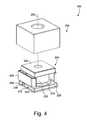
- FIG. 4is a perspective view of the camera module of FIG. 1 with an outer casing removed;
- FIG. 5is an exploded perspective view of an alternate camera module
- FIG. 6is bottom perspective view of a chip carrier of the camera module of FIG. 5 ;
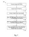
- FIG. 7is a flow chart summarizing an example method for manufacturing a camera module.
- the present inventionovercomes the problems associated with the prior art, by providing a novel method of manufacturing a miniature camera module, optionally with an autofocus and/or zoom feature.
- numerous specific detailsare set forth (e.g., various flexible circuit substrate shapes, various active/passive components, etc.) in order to provide a thorough understanding of the invention. Those skilled in the art will recognize, however, that the invention may be practiced apart from these specific details. In other instances, details of well known electronic assembly practices and components have been omitted, so as not to unnecessarily obscure the present invention.
- FIG. 1is a perspective view of a camera module 100 according to one embodiment of the present invention.
- Camera module 100is shown mounted on a portion of a printed circuit board (PCB) 102 that represents a PCB of a camera hosting device (e.g., a main board of a cell phone).
- PCBprinted circuit board
- Device 106represents an electronic component (e.g., passive or active electronic component) that may be mounted directly on PCB 102 .
- PCB 102 , traces 104 , and device 106are representational in character only.
- FIG. 2is an exploded view of camera module 100 showing a flexible printed circuit (FPC) 200 , a housing 202 , a lens assembly 204 , and an outer casing 206 exploded along an optical axis 208 .
- FPCflexible printed circuit
- FPC 200includes a first portion 210 , a second portion 212 , and an intermediate portion 214 .
- intermediate portion 214is flexed such that second portion 212 is positioned above first portion 210 .
- second portion 212is positioned above first portion 210 around housing 202 in planes that are substantially perpendicular to first portion 210 .
- First portion 210provides a surface for mounting an image capture device 216 and other passive or active electronic components 218 .
- Image capture deviceincludes a planar image capture surface 220 which is perpendicular to optical axis 208 .
- First portion 210is shown fixed to a stiffener 222 to provide rigidity.
- Second portion 212provides a surface for mounting various other electronic components 224 .
- Second portion 212is shown fixed to a set of stiffeners 226 to provide rigidity.
- Intermediate portion 214includes circuitry (not shown) which provides a path for electrical communication between first portion 210 and second portion 212 .
- camera module 100could be mounted to host device 102 by various means.
- FPC 200could include a third portion extending off first portion 210 , which is then folded 180 degrees such that a set of contacts formed thereon would face PCB 102 and facilitate electrical connection thereto.
- first portion 210could include a plurality of vias leading to a respective set of contacts formed on the rear surface of first portion 210 .
- Housing 202includes a base 228 and an outer wall 230 extending upwardly along optical axis 208 .
- Base 228is adapted to mount on first portion 210 over image capture device 216 to protect image capture surface 220 from debris and other contaminants.
- Outer wall 230provides support to lens assembly 204 .
- outer wall 230engages lens assembly 204 so as to fixably mount lens assembly 204 with respect to image capture device 216 .
- housing 202can be formed before it is mounted over image capture device 216 .
- housing 202can be formed (e.g., molded) directly over image capture device 216 and electronic components 218 .
- Lens assembly 204includes a barrel 232 extending downwardly from an actuator 234 along optical axis 208 .
- Barrel 323encloses a set of lenses coaxially aligned along optical axis 208 .
- Actuator 234includes both a movable lens and an electrical lens driving means which, when actuated, moves the lens along optical axis 208 . Indeed, this change in vertical displacement between the movable lens and image capture surface 220 results in a change in focal field and/or zoom of camera module 100 .
- actuator 234is electrically connected to FPC 200 via a second FPC 236 , which includes a first end 238 and a second end 240 .
- First end 238is adapted to electrically connect to actuator 234
- second end 240is adapted to connect to FPC 200 .
- FPC 236can be a separate FPC or can be a third portion of FPC 200 extended upwardly.
- Outer casing 206is a rigid boxlike structure which provides support to and protects the inner components of camera module 100 .
- Outer casing 206includes an inner surface (not shown) which surrounds and engages second portion 212 of FPC 200 .
- outer casingprevents second portion 212 from moving freely, because FPC's have a tendency to move back to their original form (memory) if no support is present.
- Outer casingfurther provides rigidity to camera module 100 so that it can be handled without damaging sensitive components.
- FIG. 3shows a perspective view of FPC 200 before second portion 212 is flexed upwardly above first portion 210 .
- first portion 210 and second portion 212are coplanar and part of a single substrate.
- Image capture device 216 , electronic components 218 and electronic components 224are all mounted on a top surface 300 of FPC 200
- stiffeners 222 and 226are mounted to a rear surface 302 of FPC 200 .
- Mounting stiffeners 222 and 226 before mounting electronic components 218 and 224provides an advantage, because the rigidity of stiffeners 222 and 226 provides support during the process of mounting electronic components 218 and 224 .
- electronic components 218 and 224can include any type of electronic component (e.g., actuator chip, processor, ROM, RAM, transistors, etc.). Therefore, electronic components 218 and 224 are representational in character only.
- FIG. 4shows a perspective view of camera module 100 with outer casing 206 removed.
- housing 202is mounted on top surface 300 of first portion 210 .
- Second portion 212is then folded upward and around barrel 232 between actuator 234 and housing 202 .
- outer casing 206is mounted to the top surface of base 228 such that the inner walls (not shown) engage stiffeners 226 and hold second portion 212 in position.
- first portion 210 of FPC 200defines the footprint parameters of camera module 100 .
- FIG. 5shows a perspective view of an alternate camera module 500 exploded along an optical axis 502 .
- Camera module 500includes: an FPC 504 , an anisotropic conductive film (ACF) 506 , a group of electronic components 508 , a ceramic substrate 510 , an image capture device 512 , a housing 514 , a lens assembly 516 , and an outer casing 518 .
- ACFanisotropic conductive film
- FPC 504is a rigid-flex printed circuit board including a first portion 522 and a second portion 524 .
- Rigid-flex circuit substrateis a single flexible circuit substrate including a thin flexible portion and a thicker, more rigid portion.
- second portion 524is the thin flexible portion
- first portion 522is the thicker more rigid portion.
- First portion 522includes a pin connector 526 formed on a top surface 528 of FPC 504 to facilitate the electrical connection between a host device and camera module 500 .
- first portion 522includes a rear surface 530 which is coupled to a stiffener 532 for providing rigidity when electrical connector 526 is electrically and physically connected to a host device.
- Second portion 524includes a set of parallel surfaces flexed upward into a plane which is perpendicular to first portion 522 so as to provide a surface to mount a set of electronic components 534 which does not consume footprint area.
- a set of stiffeners 536is shown mounted to rear 530 of second portion 524 to provide rigidity.
- ACF 506provides a means for electrically and physically connecting ceramic substrate 510 to FPC 504 .
- a rear surface 538 of ceramic substrate 510is coupled to top surface 528 of first portion 522 .
- ACF 506is an anisotropic conductive film commonly known to those skilled in the art for simultaneously adhering and electrically connecting surfaces.
- Electronic components 508are mounted on rear surface 538 within a cavity 540 (shown in FIG. 6 ) formed on ceramic substrate 510 .
- Image capture device 512is mounted on a top surface 542 of ceramic substrate 510 .
- Image capture device 512 , housing 514 , lens assembly 516 , FPC 520 , and outer casing 518 of FIG. 5are substantially the same as image capture device 216 , housing 202 , lens assembly 204 , FPC 236 , and outer casing 206 of FIG. 2 , respectively. Therefore, these components will not be described in detail, so as to avoid unnecessary repetitiveness.
- FIG. 6is a perspective view of ceramic substrate 510 showing electronic components 508 mounted on rear surface 538 .
- Electronic components 508are shown mounted within cavity 540 .
- Electronic components 508can be mounted to rear surface 538 via any method known to those skilled in the art. Such methods include, but are not limited to, surface mount reflow, flip-chip assembly, and wire bonding with or without overmolding.
- the depth of cavity 540is greater than the height of electronic components 508 such that the planarity between rear surface 538 and a circuit substrate are not altered by electronic components 508 .
- electronic components 508could include various different devices including but not limited to: an actuator driver chip, EE-PROM, etc.
- Rear surface 538further includes a set of contact pads 600 formed thereon to facilitate the electrical connection of ceramic substrate 510 to a circuit substrate.
- electronic components 508can even include ICD 512 .
- ceramic substrate 510defines an aperture through which lens assembly 516 can focus an image onto the image capture surface of ICD 512 , which is flip-chip mounted onto rear surface 538 .
- FIG. 7is a flow chart 700 describing a method for manufacturing a camera module.
- a first step 702an image capture device is provided.
- an electronic componentis provided in a second step 704 .
- a flexible circuit substrateis provided in a third step 706 .
- the image capture deviceis mounted on a first portion of the flexible circuit substrate.
- the electronic componentis mounted on the second portion of the flexible circuit substrate.
- the second portion of the flexible circuit substrateis positioned above the first portion of the flexible circuit substrate.
Landscapes
- Engineering & Computer Science (AREA)
- Multimedia (AREA)
- Signal Processing (AREA)
- Studio Devices (AREA)
- Camera Bodies And Camera Details Or Accessories (AREA)
- Lens Barrels (AREA)
- Transforming Light Signals Into Electric Signals (AREA)
Abstract
Description
Claims (40)
Priority Applications (7)
| Application Number | Priority Date | Filing Date | Title |
|---|---|---|---|
| US12/590,325US8248523B2 (en) | 2009-11-05 | 2009-11-05 | Camera module with fold over flexible circuit and cavity substrate |
| CA2780157ACA2780157A1 (en) | 2009-11-05 | 2010-11-05 | Camera module with fold-over flexible circuit and cavity substrate |
| EP10828667.5AEP2496988B1 (en) | 2009-11-05 | 2010-11-05 | Camera module with fold-over flexible circuit and cavity substrate |
| CN201080060668.5ACN102695985B (en) | 2009-11-05 | 2010-11-05 | There is camera model and the manufacture method thereof of folding type flexible circuit and cavity substrate |
| JP2012537862AJP5632006B2 (en) | 2009-11-05 | 2010-11-05 | The camera module |
| PCT/US2010/002913WO2011056228A1 (en) | 2009-11-05 | 2010-11-05 | Camera module with fold-over flexible circuit and cavity substrate |
| JP2014162236AJP5827385B2 (en) | 2009-11-05 | 2014-08-08 | The camera module |
Applications Claiming Priority (1)
| Application Number | Priority Date | Filing Date | Title |
|---|---|---|---|
| US12/590,325US8248523B2 (en) | 2009-11-05 | 2009-11-05 | Camera module with fold over flexible circuit and cavity substrate |
Publications (2)
| Publication Number | Publication Date |
|---|---|
| US20110102667A1 US20110102667A1 (en) | 2011-05-05 |
| US8248523B2true US8248523B2 (en) | 2012-08-21 |
Family
ID=43925059
Family Applications (1)
| Application Number | Title | Priority Date | Filing Date |
|---|---|---|---|
| US12/590,325Expired - Fee RelatedUS8248523B2 (en) | 2009-11-05 | 2009-11-05 | Camera module with fold over flexible circuit and cavity substrate |
Country Status (6)
| Country | Link |
|---|---|
| US (1) | US8248523B2 (en) |
| EP (1) | EP2496988B1 (en) |
| JP (2) | JP5632006B2 (en) |
| CN (1) | CN102695985B (en) |
| CA (1) | CA2780157A1 (en) |
| WO (1) | WO2011056228A1 (en) |
Cited By (12)
| Publication number | Priority date | Publication date | Assignee | Title |
|---|---|---|---|---|
| US20110261253A1 (en)* | 2010-04-26 | 2011-10-27 | Hon Hai Precision Industry Co., Ltd. | Camera module |
| US20120075518A1 (en)* | 2010-09-29 | 2012-03-29 | Hoya Corporation | Imaging unit |
| US20120140101A1 (en)* | 2009-06-29 | 2012-06-07 | Lensvector, Inc. | Wafer level camera module with active optical element |
| US8545114B2 (en) | 2011-03-11 | 2013-10-01 | Digitaloptics Corporation | Auto focus-zoom actuator or camera module contamination reduction feature with integrated protective membrane |
| US8605208B2 (en) | 2007-04-24 | 2013-12-10 | Digitaloptics Corporation | Small form factor modules using wafer level optics with bottom cavity and flip-chip assembly |
| US20140310952A1 (en)* | 2013-04-22 | 2014-10-23 | Hon Hai Precision Industry Co., Ltd. | Device for assembling camera module having anisotropic conductive film |
| US9088705B1 (en) | 2013-08-30 | 2015-07-21 | Amazon Technologies, Inc. | Camera module package with stiffener-mounted image sensor die |
| US9241097B1 (en) | 2013-09-27 | 2016-01-19 | Amazon Technologies, Inc. | Camera module including image sensor die in molded cavity substrate |
| CN110839124A (en)* | 2018-08-16 | 2020-02-25 | 三赢科技(深圳)有限公司 | Lens module and assembling method thereof |
| US10925160B1 (en) | 2016-06-28 | 2021-02-16 | Amazon Technologies, Inc. | Electronic device with a display assembly and silicon circuit board substrate |
| US11146712B2 (en)* | 2017-09-21 | 2021-10-12 | Robert Bosch Gmbh | Method for manufacturing camera modules and a camera module array |
| US12295097B1 (en) | 2020-12-28 | 2025-05-06 | Waymo Llc | Compact ceramic package with rear cavities |
Families Citing this family (52)
| Publication number | Priority date | Publication date | Assignee | Title |
|---|---|---|---|---|
| JP5934109B2 (en)* | 2010-01-11 | 2016-06-15 | フレクストロニクス エイピー エルエルシーFlextronics Ap,Llc | Camera module with molded tape flip chip imaging device mounting and manufacturing method |
| US8970781B2 (en)* | 2010-05-20 | 2015-03-03 | Lg Innotek Co., Ltd. | Camera module having MEMS actuator, connecting method for shutter coil of camera module and camera module manufactured by the same method |
| JP5607830B2 (en)* | 2011-07-29 | 2014-10-15 | 富士フイルム株式会社 | Cover for taking lens device |
| US8913180B2 (en) | 2011-09-29 | 2014-12-16 | Flextronics Ap, Llc | Folded tape package for electronic devices |
| US20130128106A1 (en)* | 2011-11-23 | 2013-05-23 | Flextronics Ap, Llc | Camera module housing having molded tape substrate with folded leads |
| US8717487B2 (en) | 2012-08-10 | 2014-05-06 | Digitaloptics Corporation | Camera module with compact sponge absorbing design |
| US9001268B2 (en) | 2012-08-10 | 2015-04-07 | Nan Chang O-Film Optoelectronics Technology Ltd | Auto-focus camera module with flexible printed circuit extension |
| WO2014026202A2 (en)* | 2012-08-10 | 2014-02-13 | Digitaloptics Corporation | Auto-focus camera module with flexible printed circuit extension |
| US9007520B2 (en) | 2012-08-10 | 2015-04-14 | Nanchang O-Film Optoelectronics Technology Ltd | Camera module with EMI shield |
| US9513458B1 (en) | 2012-10-19 | 2016-12-06 | Cognex Corporation | Carrier frame and circuit board for an electronic device with lens backlash reduction |
| US9746636B2 (en) | 2012-10-19 | 2017-08-29 | Cognex Corporation | Carrier frame and circuit board for an electronic device |
| CN103813070A (en)* | 2012-11-14 | 2014-05-21 | 鸿富锦精密工业(深圳)有限公司 | Imaging device |
| KR101634516B1 (en) | 2013-06-13 | 2016-06-28 | 코어포토닉스 리미티드 | Dual aperture zoom digital camera |
| US9857568B2 (en) | 2013-07-04 | 2018-01-02 | Corephotonics Ltd. | Miniature telephoto lens assembly |
| JP2016523389A (en) | 2013-07-04 | 2016-08-08 | コアフォトニクス リミテッド | Compact telephoto lens assembly |
| US9497364B2 (en) | 2013-09-13 | 2016-11-15 | Lg Innotek Co., Ltd. | Camera module |
| WO2015104960A1 (en)* | 2014-01-09 | 2015-07-16 | 富士フイルム株式会社 | Imaging module, imaging module production method, and electronic device |
| KR102214401B1 (en)* | 2014-02-28 | 2021-02-09 | 삼성전자주식회사 | Module device |
| US9392188B2 (en) | 2014-08-10 | 2016-07-12 | Corephotonics Ltd. | Zoom dual-aperture camera with folded lens |
| CN105572840B (en)* | 2014-11-11 | 2018-11-30 | 信泰光学(深圳)有限公司 | It is thinned optical lens |
| CN112433331B (en) | 2015-01-03 | 2022-07-08 | 核心光电有限公司 | Miniature telephoto lens module and camera using the same |
| US10447900B2 (en)* | 2015-08-06 | 2019-10-15 | Apple Inc. | Camera module design with lead frame and plastic moulding |
| WO2017130887A1 (en)* | 2016-01-28 | 2017-08-03 | オリンパス株式会社 | Imaging unit, imaging module, and endoscope |
| TWI618949B (en)* | 2016-04-01 | 2018-03-21 | 台灣東電化股份有限公司 | Lens driving mechanism and control method thereof |
| KR102212611B1 (en) | 2017-02-23 | 2021-02-05 | 코어포토닉스 리미티드 | Folded camera lens designs |
| US10257933B1 (en)* | 2017-09-26 | 2019-04-09 | Google Llc | Transverse circuit board to route electrical traces |
| KR102473235B1 (en)* | 2017-09-29 | 2022-12-02 | 엘지이노텍 주식회사 | Lens driving device, camera module and optical apparatus |
| DE102018126795A1 (en)* | 2018-10-26 | 2020-04-30 | Hoya Corporation | Endoscope with circuit board |
| JP7295375B2 (en)* | 2018-12-14 | 2023-06-21 | ミツミ電機株式会社 | LENS DRIVING DEVICE, CAMERA MODULE, AND CAMERA MOUNTING DEVICE |
| US11962883B2 (en)* | 2018-12-14 | 2024-04-16 | Mitsumi Electric Co., Ltd. | Lens driving device, camera module, and camera mounting device |
| US11336830B2 (en) | 2019-01-03 | 2022-05-17 | Corephotonics Ltd. | Multi-aperture cameras with at least one two state zoom camera |
| WO2021033047A1 (en) | 2019-08-21 | 2021-02-25 | Corephotonics Ltd. | Low total track length for large sensor format |
| WO2021048307A1 (en)* | 2019-09-10 | 2021-03-18 | Fn Herstal S.A. | Imaging system for firearm |
| US12072609B2 (en) | 2019-09-24 | 2024-08-27 | Corephotonics Ltd. | Slim pop-out cameras and lenses for such cameras |
| US11656538B2 (en) | 2019-11-25 | 2023-05-23 | Corephotonics Ltd. | Folded zoom camera module with adaptive aperture |
| US11770609B2 (en) | 2020-05-30 | 2023-09-26 | Corephotonics Ltd. | Systems and methods for obtaining a super macro image |
| KR102765964B1 (en) | 2020-07-22 | 2025-02-07 | 코어포토닉스 리미티드 | Folded camera lens design |
| CN214586259U (en)* | 2020-07-24 | 2021-11-02 | 台湾东电化股份有限公司 | Optical system |
| CN119414645A (en) | 2020-07-31 | 2025-02-11 | 核心光电有限公司 | camera |
| KR102380310B1 (en)* | 2020-08-26 | 2022-03-30 | 삼성전기주식회사 | Camera Module |
| EP4127788A4 (en) | 2020-09-18 | 2024-06-19 | Corephotonics Ltd. | Pop-out zoom camera |
| US12271105B2 (en) | 2020-11-05 | 2025-04-08 | Corephotonics Ltd. | Scanning Tele camera based on two prism field of view scanning |
| KR20250008791A (en) | 2020-12-01 | 2025-01-15 | 코어포토닉스 리미티드 | Folded camera with continuously adaptive zoom factor |
| CN117425062A (en) | 2021-01-25 | 2024-01-19 | 核心光电有限公司 | Lens system for compact digital camera |
| WO2022200965A1 (en) | 2021-03-22 | 2022-09-29 | Corephotonics Ltd. | Folded cameras with continuously adaptive zoom factor |
| KR20240012438A (en) | 2021-06-23 | 2024-01-29 | 코어포토닉스 리미티드 | Compact folded tele camera |
| KR102685591B1 (en) | 2021-09-23 | 2024-07-15 | 코어포토닉스 리미티드 | Large aperture continuous zoom folded telecamera |
| CN119414565A (en) | 2021-11-02 | 2025-02-11 | 核心光电有限公司 | Camera module and mobile device |
| CN120315167A (en) | 2021-12-14 | 2025-07-15 | 核心光电有限公司 | Large aperture compact scan telephoto camera |
| US12368960B2 (en) | 2022-08-05 | 2025-07-22 | Corephotonics Ltd. | Systems and methods for zoom digital camera with automatic adjustable zoom field of view |
| CN117692745A (en)* | 2022-08-31 | 2024-03-12 | 信扬科技(佛山)有限公司 | Lens module and electronic device |
| CN118317183B (en)* | 2024-06-04 | 2024-11-29 | 宁波舜宇光电信息有限公司 | Base of periscope camera module, manufacturing method and periscope camera module |
Citations (6)
| Publication number | Priority date | Publication date | Assignee | Title |
|---|---|---|---|---|
| US20050040510A1 (en)* | 1999-10-01 | 2005-02-24 | Seiko Epson Corporation | Interconnect substrate, semiconductor device, methods of fabricating, inspecting, and mounting the semiconductor device, circuit board, and electronic instrument |
| US20050285973A1 (en)* | 2004-06-25 | 2005-12-29 | Harpuneet Singh | System and method for mounting an image capture device on a flexible substrate |
| US20060087017A1 (en)* | 2004-10-21 | 2006-04-27 | Chipmos Technologies (Bermuda) Ltd. | Image sensor package |
| US20060223216A1 (en)* | 2005-03-29 | 2006-10-05 | Chin-Huang Chang | Sensor module structure and method for fabricating the same |
| US20080170141A1 (en)* | 2007-01-11 | 2008-07-17 | Samuel Waising Tam | Folded package camera module and method of manufacture |
| US20080267617A1 (en)* | 2007-04-27 | 2008-10-30 | Hon Hai Precision Industry Co., Ltd. | Electrical connector and camera device having the same |
Family Cites Families (11)
| Publication number | Priority date | Publication date | Assignee | Title |
|---|---|---|---|---|
| KR100270869B1 (en)* | 1997-10-10 | 2001-01-15 | 윤종용 | 3D Composite Circuit Board |
| JP3952897B2 (en)* | 2002-07-31 | 2007-08-01 | 日本電気株式会社 | Camera module and portable communication terminal using the same |
| JP4395859B2 (en)* | 2003-01-07 | 2010-01-13 | 三星電機株式会社 | Camera module for portable terminals |
| JP2004274164A (en)* | 2003-03-05 | 2004-09-30 | Seiko Epson Corp | Optical module, method of manufacturing the same, and electronic device |
| JP4276678B2 (en)* | 2004-07-28 | 2009-06-10 | 富士通マイクロエレクトロニクス株式会社 | Imaging device |
| JP2007041419A (en) | 2005-08-04 | 2007-02-15 | Konica Minolta Opto Inc | Supporting mechanism, imaging apparatus using the same, and structure and method for attaching flexible board |
| JP2007174380A (en)* | 2005-12-22 | 2007-07-05 | Citizen Electronics Co Ltd | Arrangement structure of camera module |
| JP2007274624A (en) | 2006-03-31 | 2007-10-18 | Citizen Miyota Co Ltd | Camera module |
| JP5004669B2 (en)* | 2007-05-28 | 2012-08-22 | 京セラ株式会社 | Imaging component, imaging unit, and manufacturing method thereof |
| US8564716B2 (en)* | 2007-11-21 | 2013-10-22 | Lg Innotek Co., Ltd. | Camera module |
| KR100982266B1 (en)* | 2008-04-24 | 2010-09-14 | 삼성전기주식회사 | Lens drive module |
- 2009
- 2009-11-05USUS12/590,325patent/US8248523B2/ennot_activeExpired - Fee Related
- 2010
- 2010-11-05JPJP2012537862Apatent/JP5632006B2/ennot_activeExpired - Fee Related
- 2010-11-05CACA2780157Apatent/CA2780157A1/ennot_activeAbandoned
- 2010-11-05EPEP10828667.5Apatent/EP2496988B1/enactiveActive
- 2010-11-05CNCN201080060668.5Apatent/CN102695985B/enactiveActive
- 2010-11-05WOPCT/US2010/002913patent/WO2011056228A1/enactiveApplication Filing
- 2014
- 2014-08-08JPJP2014162236Apatent/JP5827385B2/ennot_activeExpired - Fee Related
Patent Citations (6)
| Publication number | Priority date | Publication date | Assignee | Title |
|---|---|---|---|---|
| US20050040510A1 (en)* | 1999-10-01 | 2005-02-24 | Seiko Epson Corporation | Interconnect substrate, semiconductor device, methods of fabricating, inspecting, and mounting the semiconductor device, circuit board, and electronic instrument |
| US20050285973A1 (en)* | 2004-06-25 | 2005-12-29 | Harpuneet Singh | System and method for mounting an image capture device on a flexible substrate |
| US20060087017A1 (en)* | 2004-10-21 | 2006-04-27 | Chipmos Technologies (Bermuda) Ltd. | Image sensor package |
| US20060223216A1 (en)* | 2005-03-29 | 2006-10-05 | Chin-Huang Chang | Sensor module structure and method for fabricating the same |
| US20080170141A1 (en)* | 2007-01-11 | 2008-07-17 | Samuel Waising Tam | Folded package camera module and method of manufacture |
| US20080267617A1 (en)* | 2007-04-27 | 2008-10-30 | Hon Hai Precision Industry Co., Ltd. | Electrical connector and camera device having the same |
Cited By (16)
| Publication number | Priority date | Publication date | Assignee | Title |
|---|---|---|---|---|
| US8605208B2 (en) | 2007-04-24 | 2013-12-10 | Digitaloptics Corporation | Small form factor modules using wafer level optics with bottom cavity and flip-chip assembly |
| US20120140101A1 (en)* | 2009-06-29 | 2012-06-07 | Lensvector, Inc. | Wafer level camera module with active optical element |
| US8891006B2 (en)* | 2009-06-29 | 2014-11-18 | Lensvector, Inc. | Wafer level camera module with active optical element |
| US20110261253A1 (en)* | 2010-04-26 | 2011-10-27 | Hon Hai Precision Industry Co., Ltd. | Camera module |
| US20120075518A1 (en)* | 2010-09-29 | 2012-03-29 | Hoya Corporation | Imaging unit |
| US8545114B2 (en) | 2011-03-11 | 2013-10-01 | Digitaloptics Corporation | Auto focus-zoom actuator or camera module contamination reduction feature with integrated protective membrane |
| US20140310952A1 (en)* | 2013-04-22 | 2014-10-23 | Hon Hai Precision Industry Co., Ltd. | Device for assembling camera module having anisotropic conductive film |
| US9223145B2 (en)* | 2013-04-22 | 2015-12-29 | Hong Fu Jin Precision Industry (Shenzhen) Co., Ltd. | Device for assembling camera module having anisotropic conductive film |
| US9167161B1 (en) | 2013-08-30 | 2015-10-20 | Amazon Technologies, Inc. | Camera module package with a folded substrate and laterally positioned components |
| US9204025B1 (en) | 2013-08-30 | 2015-12-01 | Amazon Technologies, Inc. | Camera module with a molded enclosure contained in a flexible substrate |
| US9088705B1 (en) | 2013-08-30 | 2015-07-21 | Amazon Technologies, Inc. | Camera module package with stiffener-mounted image sensor die |
| US9241097B1 (en) | 2013-09-27 | 2016-01-19 | Amazon Technologies, Inc. | Camera module including image sensor die in molded cavity substrate |
| US10925160B1 (en) | 2016-06-28 | 2021-02-16 | Amazon Technologies, Inc. | Electronic device with a display assembly and silicon circuit board substrate |
| US11146712B2 (en)* | 2017-09-21 | 2021-10-12 | Robert Bosch Gmbh | Method for manufacturing camera modules and a camera module array |
| CN110839124A (en)* | 2018-08-16 | 2020-02-25 | 三赢科技(深圳)有限公司 | Lens module and assembling method thereof |
| US12295097B1 (en) | 2020-12-28 | 2025-05-06 | Waymo Llc | Compact ceramic package with rear cavities |
Also Published As
| Publication number | Publication date |
|---|---|
| US20110102667A1 (en) | 2011-05-05 |
| CA2780157A1 (en) | 2011-05-12 |
| JP2013510503A (en) | 2013-03-21 |
| EP2496988B1 (en) | 2020-10-07 |
| CN102695985A (en) | 2012-09-26 |
| EP2496988A4 (en) | 2014-09-03 |
| JP5827385B2 (en) | 2015-12-02 |
| CN102695985B (en) | 2015-09-09 |
| EP2496988A1 (en) | 2012-09-12 |
| JP2014212577A (en) | 2014-11-13 |
| JP5632006B2 (en) | 2014-11-26 |
| WO2011056228A1 (en) | 2011-05-12 |
Similar Documents
| Publication | Publication Date | Title |
|---|---|---|
| US8248523B2 (en) | Camera module with fold over flexible circuit and cavity substrate | |
| CA2675179C (en) | Folded package camera module and method of manufacture | |
| KR102390760B1 (en) | Camera device and electronic device therefof | |
| US20090161006A1 (en) | Image sensor, method of manufacturing the same, and camera module having the same | |
| US20110285890A1 (en) | Camera module | |
| US20080142917A1 (en) | Image sensor module, method of manufacturing the same, and camera module having the same | |
| KR101133135B1 (en) | Image sensor module and camera module comprising the same | |
| US10009528B2 (en) | Autofocus camera module packaging with circuitry-integrated actuator system | |
| KR101661660B1 (en) | Camera module | |
| US7429783B2 (en) | Image sensor package | |
| US20070173084A1 (en) | Board-to-board connecting structure | |
| KR100770430B1 (en) | Camera module | |
| US8049809B2 (en) | Solid-state image pickup device and electronic instruments | |
| KR20060104962A (en) | Device for camera module | |
| KR100752708B1 (en) | Camera module package | |
| KR100947967B1 (en) | Camera module and its manufacturing method | |
| KR200464059Y1 (en) | Camera module | |
| KR100803275B1 (en) | Camera device and its manufacturing method | |
| KR20090015697A (en) | Camera Module Package | |
| KR100772586B1 (en) | Camera module | |
| KR101009147B1 (en) | Printed Circuit Boards with Side Connectors | |
| KR102118452B1 (en) | Camera module | |
| KR101003597B1 (en) | Camera module | |
| KR20090128272A (en) | Camera module and manufacturing method of the same |
Legal Events
| Date | Code | Title | Description |
|---|---|---|---|
| AS | Assignment | Owner name:FLEXTRONICS AP LLC, COLORADO Free format text:ASSIGNMENT OF ASSIGNORS INTEREST;ASSIGNORS:CHUA, ALBERT JOHN Y.;LIMAYE, ABHIJIT;SIGNING DATES FROM 20100328 TO 20100329;REEL/FRAME:025234/0700 | |
| ZAAA | Notice of allowance and fees due | Free format text:ORIGINAL CODE: NOA | |
| ZAAB | Notice of allowance mailed | Free format text:ORIGINAL CODE: MN/=. | |
| STCF | Information on status: patent grant | Free format text:PATENTED CASE | |
| AS | Assignment | Owner name:DIGITALOPTICS CORPORATION, CALIFORNIA Free format text:ASSIGNMENT OF ASSIGNORS INTEREST;ASSIGNOR:FLEXTRONICS AP, LLC;REEL/FRAME:028948/0790 Effective date:20120628 | |
| AS | Assignment | Owner name:NAN CHANG O-FILM OPTOELECTRONICS TECHNOLOGY LTD, C Free format text:ASSIGNMENT OF ASSIGNORS INTEREST;ASSIGNORS:DIGITALOPTICS CORPORATION;DIGITALOPTICS CORPORATION MEMS;FOTONATION LIMITED;REEL/FRAME:034883/0237 Effective date:20141114 | |
| FEPP | Fee payment procedure | Free format text:PAYOR NUMBER ASSIGNED (ORIGINAL EVENT CODE: ASPN); ENTITY STATUS OF PATENT OWNER: LARGE ENTITY | |
| FPAY | Fee payment | Year of fee payment:4 | |
| MAFP | Maintenance fee payment | Free format text:PAYMENT OF MAINTENANCE FEE, 8TH YEAR, LARGE ENTITY (ORIGINAL EVENT CODE: M1552); ENTITY STATUS OF PATENT OWNER: LARGE ENTITY Year of fee payment:8 | |
| FEPP | Fee payment procedure | Free format text:MAINTENANCE FEE REMINDER MAILED (ORIGINAL EVENT CODE: REM.); ENTITY STATUS OF PATENT OWNER: LARGE ENTITY | |
| LAPS | Lapse for failure to pay maintenance fees | Free format text:PATENT EXPIRED FOR FAILURE TO PAY MAINTENANCE FEES (ORIGINAL EVENT CODE: EXP.); ENTITY STATUS OF PATENT OWNER: LARGE ENTITY | |
| STCH | Information on status: patent discontinuation | Free format text:PATENT EXPIRED DUE TO NONPAYMENT OF MAINTENANCE FEES UNDER 37 CFR 1.362 | |
| FP | Lapsed due to failure to pay maintenance fee | Effective date:20240821 |