US8248211B2 - Selective RF device activation - Google Patents
Selective RF device activationDownload PDFInfo
- Publication number
- US8248211B2 US8248211B2US11/186,666US18666605AUS8248211B2US 8248211 B2US8248211 B2US 8248211B2US 18666605 AUS18666605 AUS 18666605AUS 8248211 B2US8248211 B2US 8248211B2
- Authority
- US
- United States
- Prior art keywords
- activate
- mask
- value
- field
- length
- Prior art date
- Legal status (The legal status is an assumption and is not a legal conclusion. Google has not performed a legal analysis and makes no representation as to the accuracy of the status listed.)
- Active, expires
Links
Images


Classifications
- G—PHYSICS
- G06—COMPUTING OR CALCULATING; COUNTING
- G06K—GRAPHICAL DATA READING; PRESENTATION OF DATA; RECORD CARRIERS; HANDLING RECORD CARRIERS
- G06K19/00—Record carriers for use with machines and with at least a part designed to carry digital markings
- G06K19/06—Record carriers for use with machines and with at least a part designed to carry digital markings characterised by the kind of the digital marking, e.g. shape, nature, code
- G06K19/067—Record carriers with conductive marks, printed circuits or semiconductor circuit elements, e.g. credit or identity cards also with resonating or responding marks without active components
- G06K19/07—Record carriers with conductive marks, printed circuits or semiconductor circuit elements, e.g. credit or identity cards also with resonating or responding marks without active components with integrated circuit chips
- G06K19/0701—Record carriers with conductive marks, printed circuits or semiconductor circuit elements, e.g. credit or identity cards also with resonating or responding marks without active components with integrated circuit chips at least one of the integrated circuit chips comprising an arrangement for power management
- G06K19/0702—Record carriers with conductive marks, printed circuits or semiconductor circuit elements, e.g. credit or identity cards also with resonating or responding marks without active components with integrated circuit chips at least one of the integrated circuit chips comprising an arrangement for power management the arrangement including a battery
- G06K19/0705—Record carriers with conductive marks, printed circuits or semiconductor circuit elements, e.g. credit or identity cards also with resonating or responding marks without active components with integrated circuit chips at least one of the integrated circuit chips comprising an arrangement for power management the arrangement including a battery the battery being connected to a power saving arrangement
- G—PHYSICS
- G06—COMPUTING OR CALCULATING; COUNTING
- G06F—ELECTRIC DIGITAL DATA PROCESSING
- G06F1/00—Details not covered by groups G06F3/00 - G06F13/00 and G06F21/00
- G06F1/04—Generating or distributing clock signals or signals derived directly therefrom
- G06F1/12—Synchronisation of different clock signals provided by a plurality of clock generators
- G—PHYSICS
- G06—COMPUTING OR CALCULATING; COUNTING
- G06F—ELECTRIC DIGITAL DATA PROCESSING
- G06F1/00—Details not covered by groups G06F3/00 - G06F13/00 and G06F21/00
- G06F1/26—Power supply means, e.g. regulation thereof
- G06F1/32—Means for saving power
- G06F1/3203—Power management, i.e. event-based initiation of a power-saving mode
- G06F1/3206—Monitoring of events, devices or parameters that trigger a change in power modality
- G06F1/3209—Monitoring remote activity, e.g. over telephone lines or network connections
- G—PHYSICS
- G06—COMPUTING OR CALCULATING; COUNTING
- G06F—ELECTRIC DIGITAL DATA PROCESSING
- G06F1/00—Details not covered by groups G06F3/00 - G06F13/00 and G06F21/00
- G06F1/26—Power supply means, e.g. regulation thereof
- G06F1/32—Means for saving power
- G06F1/3203—Power management, i.e. event-based initiation of a power-saving mode
- G06F1/3234—Power saving characterised by the action undertaken
- G06F1/3287—Power saving characterised by the action undertaken by switching off individual functional units in the computer system
- G—PHYSICS
- G06—COMPUTING OR CALCULATING; COUNTING
- G06K—GRAPHICAL DATA READING; PRESENTATION OF DATA; RECORD CARRIERS; HANDLING RECORD CARRIERS
- G06K19/00—Record carriers for use with machines and with at least a part designed to carry digital markings
- G06K19/06—Record carriers for use with machines and with at least a part designed to carry digital markings characterised by the kind of the digital marking, e.g. shape, nature, code
- G06K19/067—Record carriers with conductive marks, printed circuits or semiconductor circuit elements, e.g. credit or identity cards also with resonating or responding marks without active components
- G06K19/07—Record carriers with conductive marks, printed circuits or semiconductor circuit elements, e.g. credit or identity cards also with resonating or responding marks without active components with integrated circuit chips
- G06K19/0701—Record carriers with conductive marks, printed circuits or semiconductor circuit elements, e.g. credit or identity cards also with resonating or responding marks without active components with integrated circuit chips at least one of the integrated circuit chips comprising an arrangement for power management
- G06K19/0707—Record carriers with conductive marks, printed circuits or semiconductor circuit elements, e.g. credit or identity cards also with resonating or responding marks without active components with integrated circuit chips at least one of the integrated circuit chips comprising an arrangement for power management the arrangement being capable of collecting energy from external energy sources, e.g. thermocouples, vibration, electromagnetic radiation
- G—PHYSICS
- G06—COMPUTING OR CALCULATING; COUNTING
- G06K—GRAPHICAL DATA READING; PRESENTATION OF DATA; RECORD CARRIERS; HANDLING RECORD CARRIERS
- G06K19/00—Record carriers for use with machines and with at least a part designed to carry digital markings
- G06K19/06—Record carriers for use with machines and with at least a part designed to carry digital markings characterised by the kind of the digital marking, e.g. shape, nature, code
- G06K19/067—Record carriers with conductive marks, printed circuits or semiconductor circuit elements, e.g. credit or identity cards also with resonating or responding marks without active components
- G06K19/07—Record carriers with conductive marks, printed circuits or semiconductor circuit elements, e.g. credit or identity cards also with resonating or responding marks without active components with integrated circuit chips
- G06K19/0701—Record carriers with conductive marks, printed circuits or semiconductor circuit elements, e.g. credit or identity cards also with resonating or responding marks without active components with integrated circuit chips at least one of the integrated circuit chips comprising an arrangement for power management
- G06K19/0712—Record carriers with conductive marks, printed circuits or semiconductor circuit elements, e.g. credit or identity cards also with resonating or responding marks without active components with integrated circuit chips at least one of the integrated circuit chips comprising an arrangement for power management the arrangement being capable of triggering distinct operating modes or functions dependent on the strength of an energy or interrogation field in the proximity of the record carrier
- G—PHYSICS
- G06—COMPUTING OR CALCULATING; COUNTING
- G06K—GRAPHICAL DATA READING; PRESENTATION OF DATA; RECORD CARRIERS; HANDLING RECORD CARRIERS
- G06K19/00—Record carriers for use with machines and with at least a part designed to carry digital markings
- G06K19/06—Record carriers for use with machines and with at least a part designed to carry digital markings characterised by the kind of the digital marking, e.g. shape, nature, code
- G06K19/067—Record carriers with conductive marks, printed circuits or semiconductor circuit elements, e.g. credit or identity cards also with resonating or responding marks without active components
- G06K19/07—Record carriers with conductive marks, printed circuits or semiconductor circuit elements, e.g. credit or identity cards also with resonating or responding marks without active components with integrated circuit chips
- G06K19/0723—Record carriers with conductive marks, printed circuits or semiconductor circuit elements, e.g. credit or identity cards also with resonating or responding marks without active components with integrated circuit chips the record carrier comprising an arrangement for non-contact communication, e.g. wireless communication circuits on transponder cards, non-contact smart cards or RFIDs
- G—PHYSICS
- G06—COMPUTING OR CALCULATING; COUNTING
- G06K—GRAPHICAL DATA READING; PRESENTATION OF DATA; RECORD CARRIERS; HANDLING RECORD CARRIERS
- G06K7/00—Methods or arrangements for sensing record carriers, e.g. for reading patterns
- G06K7/0008—General problems related to the reading of electronic memory record carriers, independent of its reading method, e.g. power transfer
- G—PHYSICS
- G06—COMPUTING OR CALCULATING; COUNTING
- G06Q—INFORMATION AND COMMUNICATION TECHNOLOGY [ICT] SPECIALLY ADAPTED FOR ADMINISTRATIVE, COMMERCIAL, FINANCIAL, MANAGERIAL OR SUPERVISORY PURPOSES; SYSTEMS OR METHODS SPECIALLY ADAPTED FOR ADMINISTRATIVE, COMMERCIAL, FINANCIAL, MANAGERIAL OR SUPERVISORY PURPOSES, NOT OTHERWISE PROVIDED FOR
- G06Q10/00—Administration; Management
- G06Q10/08—Logistics, e.g. warehousing, loading or distribution; Inventory or stock management
- H—ELECTRICITY
- H04—ELECTRIC COMMUNICATION TECHNIQUE
- H04W—WIRELESS COMMUNICATION NETWORKS
- H04W52/00—Power management, e.g. Transmission Power Control [TPC] or power classes
- H04W52/02—Power saving arrangements
- H04W52/0209—Power saving arrangements in terminal devices
- H04W52/0225—Power saving arrangements in terminal devices using monitoring of external events, e.g. the presence of a signal
- H04W52/0238—Power saving arrangements in terminal devices using monitoring of external events, e.g. the presence of a signal where the received signal is an unwanted signal, e.g. interference or idle signal
- H—ELECTRICITY
- H04—ELECTRIC COMMUNICATION TECHNIQUE
- H04W—WIRELESS COMMUNICATION NETWORKS
- H04W52/00—Power management, e.g. Transmission Power Control [TPC] or power classes
- H04W52/02—Power saving arrangements
- H04W52/0209—Power saving arrangements in terminal devices
- H04W52/0261—Power saving arrangements in terminal devices managing power supply demand, e.g. depending on battery level
- H04W52/0274—Power saving arrangements in terminal devices managing power supply demand, e.g. depending on battery level by switching on or off the equipment or parts thereof
- H04W52/028—Power saving arrangements in terminal devices managing power supply demand, e.g. depending on battery level by switching on or off the equipment or parts thereof switching on or off only a part of the equipment circuit blocks
- Y—GENERAL TAGGING OF NEW TECHNOLOGICAL DEVELOPMENTS; GENERAL TAGGING OF CROSS-SECTIONAL TECHNOLOGIES SPANNING OVER SEVERAL SECTIONS OF THE IPC; TECHNICAL SUBJECTS COVERED BY FORMER USPC CROSS-REFERENCE ART COLLECTIONS [XRACs] AND DIGESTS
- Y02—TECHNOLOGIES OR APPLICATIONS FOR MITIGATION OR ADAPTATION AGAINST CLIMATE CHANGE
- Y02D—CLIMATE CHANGE MITIGATION TECHNOLOGIES IN INFORMATION AND COMMUNICATION TECHNOLOGIES [ICT], I.E. INFORMATION AND COMMUNICATION TECHNOLOGIES AIMING AT THE REDUCTION OF THEIR OWN ENERGY USE
- Y02D10/00—Energy efficient computing, e.g. low power processors, power management or thermal management
- Y—GENERAL TAGGING OF NEW TECHNOLOGICAL DEVELOPMENTS; GENERAL TAGGING OF CROSS-SECTIONAL TECHNOLOGIES SPANNING OVER SEVERAL SECTIONS OF THE IPC; TECHNICAL SUBJECTS COVERED BY FORMER USPC CROSS-REFERENCE ART COLLECTIONS [XRACs] AND DIGESTS
- Y02—TECHNOLOGIES OR APPLICATIONS FOR MITIGATION OR ADAPTATION AGAINST CLIMATE CHANGE
- Y02D—CLIMATE CHANGE MITIGATION TECHNOLOGIES IN INFORMATION AND COMMUNICATION TECHNOLOGIES [ICT], I.E. INFORMATION AND COMMUNICATION TECHNOLOGIES AIMING AT THE REDUCTION OF THEIR OWN ENERGY USE
- Y02D30/00—Reducing energy consumption in communication networks
- Y02D30/70—Reducing energy consumption in communication networks in wireless communication networks
Definitions
- the present inventionrelates to Radio Frequency (RF) tag activation, and more particularly, this invention relates to functional activation of RF tags and other electronic RF devices.
- RFRadio Frequency
- Auto-IDAutomatic identification
- bar codewhich uses an alternating series of thin and wide bands that can be digitally interpreted by an optical scanner.
- UPCuniversal product code
- the bar codestill requires manual interrogation by a human operator to scan each tagged object individually with a scanner. This is a line-of-sight process that has inherent limitations in speed and reliability.
- the UPC bar codesonly allow for manufacturer and product type information to be encoded into the barcode, not the unique item's serial number.
- the bar code on one milk cartonis the same as every other, making it impossible to count objects or individually check expiration dates.
- RFID technologyemploys a radio frequency (“RF”) wireless link and ultra-small embedded computer chips, to overcome these barcode limitations.
- RFID technologyallows physical objects to be identified and tracked via these wireless “tags”. It functions like a bar code that communicates to the reader automatically without needing manual line-of-sight scanning or singulation of the objects.
- RFIDpromises to radically transform the retail, pharmaceutical, military, and transportation industries.
- an RFID system 100includes a tag 102 , a reader 104 , and an optional server 106 .
- the tag 102includes an IC chip and an antenna.
- the IC chipincludes a digital decoder needed to execute the computer commands that the tag 102 receives from the tag reader 104 .
- the IC chipalso includes a power supply circuit to extract and regulate power from the RF reader; a detector to decode signals from the reader; a backscatter modulator, a transmitter to send data back to the reader; anti-collision protocol circuits; and at least enough memory to store its EPC code.
- Communicationbegins with a reader 104 sending out signals to find the tag 102 .
- the reader 104decodes the data programmed into the tag 102 .
- the informationis then passed to a server 106 for processing, storage, and/or propagation to another computing device.
- RFID systemsuse reflected or “backscattered” radio frequency (RF) waves to transmit information from the tag 102 to the reader 104 . Since passive (Class-1 and Class-2) tags get all of their power from the reader signal, the tags are only powered when in the beam of the reader 104 .
- RFradio frequency
- Class-3 tagssolve this problem by incorporating batteries and signal preamplifiers to increase range. This battery will last many years if power consumption is managed well, but only a few days if power consumption is managed poorly. Because battery powered systems (also known as active devices) will coexist with passive devices, care must be taken to reduce the power drain of the battery powered systems. Class-1 RFID tags, for example, receive their operating power from the Reader (Transmitted power). The definition of Class-3 RFID devices requires distances sufficient to make this an unusable power source. Additionally, Class-3 devices must co-exist in Class-1 environments and care must be taken to manage power drain from the battery of all active or semi-active devices. If a Class-3 device continually responds to unwanted Class-1 instructions (these being commands for “other” devices) battery power will be drained extremely quickly.
- Wake up codeshave been used in RFID systems to selectively “wake up” individual tags and not others, thereby conserving the battery life of the tags that are not needed and/or reducing the amount of signal received back from a given set of tags.
- the readerbroadcasts a wake up code, and each tag activates just long enough to determine whether the broadcast code matches a code stored in the tag's memory. If the codes match, the tag fully activates. If the codes do not match, the tag returns to a hibernate state or does not respond further to the reader.
- wake up codeshas been proven to be effective at reducing overall battery consumption in Class-3 devices. However, it would be desirable to eliminate the need for all tags receiving a broadcasted wake up code to analyze the wake up code to determine whether the wake up code corresponds to that particular tag. Thus, it would be desirable to add some type of encoding to indicate early on during receipt of the wake up code whether or not to continue to analyze the rest of the wake up code string.
- the devicelistens for an activate code, the activate code having a length field and a mask field, the mask field including a mask value, the length field specifying a length of the mask field to a final bit of the mask value.
- the length fieldis compared to a stored length value for determining whether the length field meets a predefined criterion. If the length field meets the predefined criterion, an address of the activate value is loaded (if an address field is present) and the appropriate bits (mask value) of the mask field are compared to a stored activate value. An activate signal is generated if the mask value matches the stored activate value. The activate signal can be used to activate additional circuitry.
- the devicelistens for an activate code, the activate code having a length field and a mask field, the mask field including a mask value, the length field specifying a position of a final bit of the mask value in the mask field.
- the appropriate bits (mask value) of the mask fieldare compared to a stored activate value. The comparison is terminated upon comparing the final bit of the mask field as specified by the length field.
- An activate signalis generated if the mask value matches the stored activate value. The activate signal can be used to activate additional circuitry.
- a method for activating a deviceincludes receiving an activate code having an address field and a mask field, where the mask field has a mask value, wherein the address field indicates a start position of the mask value in the mask field.
- the mask valueis compared to an activate value stored on the device.
- a method for analyzing an activate code having a length field and a mask fieldincludes receiving the length field, comparing the length field to a stored length value, determining whether the length field meets a predefined criteria based on the comparison of the length field to the stored length value, receiving the mask field, the mask field having a mask value, comparing the mask value of the mask field to a stored activate value if the length field meets the predefined criteria, and generating an activate signal if the received mask value matches the stored activate value.
- a method for analyzing an activate code having an address field and a mask fieldincludes receiving the address and mask fields, where the address field indicates a location of the mask value in the mask field.
- the mask value of the mask fieldis compared to a stored activate value.
- An activate signalis generated if the received mask value matches the stored value.
- a systemcomprising an interrogator and a plurality of devices in radio frequency communication with the interrogator, wherein a first subset of the devices are responsive to an activate command of a first length, wherein a second subset of the devices are responsive to an activate command of a second length.
- a circuit for selectively generating an activate signalincludes an interrupt circuit for determining whether an interrupt period of a received signal matches a predetermined plurality of values or falls within a predetermined range, the interrupt circuit outputting an interrupt signal if the interrupt period matches the predetermined value or falls within the predetermined range.
- a data comparison circuitcompares a received activate code to a stored activate value, the activate code having a length field and a mask field, the length field specifying at least one of (i) a length of the mask field and (ii) a position of a final bit of a mask value of the mask field, the data comparison circuit generating an activate signal if the received mask value matches the stored activate value.
- a circuit for analyzing an activate code having a length field and a mask fieldincludes a data register for storing an activate value, a length counter for receiving the length field, and a data comparison circuit for comparing at least a portion of the mask field to the activate value.
- the data comparison circuitgenerates an activate signal if the portion of the mask field matches the activate value.
- a method for selectively activating a subset of a plurality of devicesincludes transmitting an activate code having a length field and a mask field, where the length field dictates which of the plurality of devices process the mask field.
- Another method for selectively activating a subset of a plurality of devicesincludes transmitting several activate codes to a plurality of remote devices, where only a subset of the devices analyze a particular one of the activate codes based upon a variable size of the code.
- FIG. 1is a system diagram of an RFID system.
- FIG. 2is a system diagram for an integrated circuit (IC) chip for implementation in an RFID tag.
- ICintegrated circuit
- FIG. 3Ais a depiction of an activate command according to one embodiment.
- FIG. 3Bis a depiction of an activate code according to one embodiment.
- FIG. 3Cis a depiction of an activate command according to another embodiment.
- FIG. 4is a diagram of an activate circuit according to one embodiment.
- FIG. 5is a circuit diagram of a mirror inverter according to one embodiment.
- FIG. 6is a circuit diagram of an exemplary current mirror according to one embodiment.
- FIG. 7is a circuit diagram of the antenna and envelope detection sections of the activate circuit of FIG. 4 according to one embodiment.
- FIG. 8is a circuit diagram of the self-biasing pre-amplifier of the activate circuit of FIG. 4 according to one embodiment.
- FIG. 9illustrates a band pass region of a signal filtered by high and low pass filters of the activate circuit.
- FIG. 10is a circuit diagram of the interrupt circuit of the activate circuit of FIG. 4 according to one embodiment.
- FIG. 11Ais a depiction of an activate command according to an embodiment.
- FIG. 11Bis a circuit diagram of the interrupt circuit of the activate circuit of FIG. 4 according to one embodiment.
- FIG. 12is a circuit diagram of a comparison circuit that compares the activate command to a stored value.
- FIG. 13is a circuit diagram of a comparison circuit that compares the activate command to multiple stored values.
- FIG. 14is a flow diagram of a method for activating a device according to one embodiment.
- RFIDRadio Frequency Identification
- pacemakersportable electronic devices
- audio devices and other electronic devicessmoke detectors; etc.
- RFIDRadio Frequency Identification
- FIG. 1To provide a context, and to aid in understanding the embodiments of the invention, much of the present description shall be presented in terms of an RFID system such as that shown in FIG. 1 . It should be kept in mind that this is done by way of example only, and the invention is not to be limited to RFID systems, as one skilled in the art will appreciate how to implement the teachings herein into electronics devices in hardware and/or software.
- Examples of hardwareinclude Application Specific Integrated Circuits (ASICs), printed circuits, monolithic circuits, reconfigurable hardware such as Field Programmable Gate Arrays (FPGAs), etc.
- ASICsApplication Specific Integrated Circuits
- FPGAsField Programmable Gate Arrays
- the methodology disclosed hereincan also be incorporated into a computer program product, such as a computer disc containing software. Further, such software can be downloadable or otherwise transferable from one computing device to another via network, nonvolatile memory device, etc.
- FIG. 2depicts a circuit layout of a Class-3 chip 200 according to an illustrative embodiment for implementation in an RFID tag.
- This Class-3 chipcan form the core of RFID chips appropriate for many applications such as identification of pallets, cartons, containers, vehicles, or anything where a range of more than 2-3 meters is desired.
- the chip 200includes several industry-standard circuits including a power generation and regulation circuit 202 , a digital command decoder and control circuit 204 , a sensor interface module 206 , a C1V2 interface protocol circuit 208 , and a power source (battery) 210 .
- a display driver module 212can be added to drive a display.
- a battery activation circuit 214is also present to act as a wake-up trigger. This circuit 214 is described in detail below.
- the battery activation circuit 214includes an ultra-low-power, narrow-bandwidth preamplifier with an ultra low power static current drain.
- the battery activation circuit 214also includes a self-clocking interrupt circuit and uses an innovative user-programmable digital wake-up code. The battery activation circuit 214 draws less power during its sleeping state and is much better protected against both accidental and malicious false wake-up trigger events that otherwise would lead to pre-mature exhaustion of the Class-3 tag battery 210 .
- a battery monitor 215can be provided to monitor power usage in the device. The information collected can then be used to estimate a useful remaining life of the battery.
- a forward link AM decoder 216uses a simplified phase-lock-loop oscillator that requires an absolute minimum amount of chip area. Preferably, the circuit 216 requires only a minimum string of reference pulses.
- a backscatter modulator block 218preferably increases the backscatter modulation depth to more than 50%.
- a memory celle.g., EEPROM is also present.
- a pure, Fowler-Nordheim direct-tunneling-through-oxide mechanism 220is present to reduce both the WRITE and ERASE currents to less than 0.1 ⁇ A/cell in the EEPROM memory array. Unlike any RFID tags built to date, this will permit designing of tags to operate at maximum range even when WRITE and ERASE operations are being performed.
- the module 200also incorporates a highly-simplified, yet very effective, security encryption circuit 222 such as the one described in US Patent Appl. entitled “SECURITY SYSTEM AND METHOD” and having Ser. No. 10/902,683, filed on Jul. 28, 2004 and which is herein incorporated by reference.
- Other security schemes, secret handshakes with readers, etc.can be used.
- connection pads(not shown) are required for the chip 200 to function: Vdd to the battery, ground, plus two antenna leads to support multi-element omni-directional antennas. Sensors to monitor temperature, shock, tampering, etc. can be added by appending an industry-standard I2C interface to the core chip.
- the battery activation circuit 214 described hereinis used in communication between two devices where a transmitter wants to activate or enable a receiving device via the Radio Frequency (RF) medium. While this circuitry anticipated for use in RFID systems, it is by no means restricted to just that industry. This disclosure describes an activation circuit where the preferred description and embodiment relates to RFID, but is by no means only restricted to that technology. Consequently, any system which requires an entity (e.g., transmitter) to alert another entity (e.g., reader) applies to this idea without regard to the medium used (e.g., RF, IR, cable, etc).
- RFRadio Frequency
- tagsmay be selectively activated, then accessed, then placed back into their hibernate (or other low power) state, and the next set of tags selectively activated. Enabling an activation selection process for large quantities of resident tags in the field at one time, but less than all tags in the field at one time, provides for the best power management strategy.
- an activation or “activate” commandis used.
- This activate commandincludes three parts. The first part is clock synchronization. The second part is an interrupt (also known as a violation). The last part is a digital user activate command code. These three parts conceptually create the activate protocol. These steps must be sufficiently separated in combination from “other normal” or common traffic as to be able to decipher the activation command from other commands or noise in, for example, Class-1, Class-2 or Class-3 devices. Each of these three components is described as follows in conjunction with FIG. 3A . It should be kept in mind that the numbers of bits, number of cycles, frequencies, memory locations, etc. can vary from those used for illustrative purposes below.
- the activate scheme described hereinis also useful in all RF devices with or without batteries for the purpose of selectively selecting individual or a subgroup of particular devices.
- the basic features of the “Activate” command 300are a:
- the Clock Sync portion 302 of the Activate command 300preferably includes a predefined clock synchronization signal at an incoming rate of, for example, 8 KHz. There needs to be a sufficient number of clock cycles to allow the receiving tag to recognize and synchronize to the incoming stream.
- the number of incoming clocks to the tagis preferably not less than 4 cycles and not greater than 10 cycles, but could be greater or smaller.
- the next sectionis the Interrupt or violation section 304 .
- Thispreferably includes two cycles of 50% duty cycle based on a 2 KHz incoming rate.
- the interruptmarks the beginning of the code section which is the third component of the Activate command.
- the receiver (tag)will realize that it has received an “Activate” command. Correct reception of the interrupt portion 304 moves the tag from the hibernate state into the code search state.
- a device (tag)preferably will only stay in the code search state for a maximum time period, such as 1-5 ms, preferably 2 ms. If the tag is not moved into the ready or active state within that time, the tag will automatically revert back into the hibernate state.
- the receiving devicelistens for the interrupt, in this example a logic 1-1 in sequence. Upon encountering any logic 1-1, the device then processes the incoming activate code 306 as described below. If a value in the next sequence of bits matches a value stored locally on the receiving device, the device wakes up (as described below). If one of the bits in the sequence fails to match, the device resets, looks for the next interrupt, and begins monitoring the sequence of bits after the next interrupt (here, logic 1-1). It should be noted that a logic 1-1 in the activate code portion 306 may cause the device to begin analyzing the incoming bit stream again. However, the code will not match and the device will reset again. So while one practicing the invention can select codes that do not result in unintended analysis, occurrence of unintended analysis should be rare. Note that codes can be predetermined that avoid unintended analysis can be predetermined and assigned. The same would apply to the bits preceding the correct interrupt.
- the activate code portion 306can be described in two parts: first the signaling or communications protocol, and second the command protocol.
- Signalingcan best be described as two different frequencies where a zero is observed as a 2 KHz tone and a one is observed as an 8 KHz tone.
- These two tones(otherwise described as FQF for frequency, quad frequency) describe a command, which when matching an internal register, move the tag from a hibernate state to an active state (ready state in the state machine).
- the activate code segmentis composed of several strings of data. This packet 306 is shown in FIG. 3B .
- the three componentsare (in order of reception at the tag) Length 322 , Address (optional) 324 , and Mask 326 .
- Each componentis described in detail below. Again, specific values are used below only for illustrative purposes, and are meant to illustrate a functional embodiment. One skilled in the art will appreciate that values and bit lengths can be increased or decreased depending on his or her preferences and in consideration of regulatory requirements. Thus, the size of the overall command is variable. Additionally, the Length 322 and Address 324 positions could potentially be switched, i.e., the Address 324 would be received before the Length 322 . Other variations could include additional fields not shown in FIG. 3B , such as a terminator value (e.g., logic 1-0-1-0) indicating the end of the Length 322 or Address 324 fields.
- a terminator valuee.g., logic 1-0-1-0
- the length field 322 in this examplecontains seven bits.
- the length field 322may contain length values from, for example, zero to 2 7 (or 128).
- the length valuespecifies the length of the Mask field 326 from zero bits up to and including the maximum length of the Mask field 326 , thereby specifying the position of the final bit of the mask value in the Mask field.
- the maximum mask lengthis 96 bits.
- the length field 322is used in conjunction with a user defined minimum mask length register (MML register) on the receiving device (tag).
- MML registerat a specified location (for example, User Memory; 0x0000) controls the minimum value which can be used for the length field 322 .
- the minimum mask length registeris the minimum amount of bits necessary to match a mask from a given starting point. If a value of length field 322 is less than the MML register, the tag will ignore the rest of the activate code 306 and will stay in the hibernate state. If the MML register is set to zero, than the length field 322 of the activate code 306 may also be set to zero.
- the mask length registermay define a maximum or exact value against which the value of the length field 322 is compared.
- the length field 322may indicate the length of the mask value in the mask field, where the address field 324 indicates where the length begins.
- a zero (or other predefined) value in the length field 322may act as a match for all devices in the field. Values of length which are greater than the maximum mask length (e.g., 96) causes the activate packet to be ignored and thus, the tag returns back to the hibernate state. In the case of a zero length value, neither the address nor mask fields will exist, thereby reducing the activate code to a seven bit field of value zero. If a value of zero is observed in the length field and the MML register allows a zero value for the length, then all devices may transition from the hibernate state to the active ready state without regard to the address or mask fields. In practice, the address and mask fields might not exist if a legal value of zero is found in the length field.
- the address field 324is optional, and in this example is also a 7 bit field. It is used in conjunction with the mask field 326 to provide an offset into the 96 bit memory reserved for the mask. If the length is set to 96, a zero offset for address is assumed, thus, no address field will be observed. For values of length less than 96, the address can be used as an offset applying the mask value received in the mask field 326 to align with the data stored in the internal mask register. In other words, the relevant mask value in the mask field 326 may begin somewhere other than the beginning of the mask field.
- the tagstays in the hibernate state, ignores the rest of the incoming activate code 306 , and waits until a new activate preamble is received.
- the mask fieldis compared against the internal activate mask register using the length and address as the number of bits to compare and the beginning offset to start the comparison.
- the internal activate mask registeris located, for example, at (User Memory; 0x30).
- the received mask value of the mask fieldis compared on a bit for bit basis. If the bits of the received mask value match the internal activate mask register, the tag will transition from the hibernate state to the active ready state. If a roll-over condition exists, that being the length of comparison has not been exhausted before the 96 th bit of the mask has been compared, the tag will interpret this as an error condition and ignore the rest of the incoming activate packet, and stay in the hibernate mode. An example of this could occur if the address indicates mask field bit 90 , and the length field indicates a mask of 10 bits. Because the mask field ends at 96 bits, the comparison rolls over the end of the mask after comparing 6 bits, and the process fails.
- the maskcan be circular. If the address and length fields cause a rollover, the comparison of mask bits continues by starting at the first bit of the mask. An example of this could occur if the address indicates mask field bit 90 , and the length field indicates a mask of 10 bits. Because the mask field ends at 96 bits, the comparison rolls over the end of the mask, so the comparison continues at the first mask bit and to the fourth mask bit. Thus, the comparison is performed in a circular manner.
- the mask fieldcan also include “dummy” bits following the mask value. Because the portion of the mask field that needs to be compared to the activate mask register is defined by the length and address sections, any additional bits following that portion have no effect on whether the device activates or not. This would allow such things as activate codes for different tags to all have a common length.
- the activate codecan be initially set at manufacturing, or can be programmed layer, such as at tag initialization. In either step, device passwords can be set to restrict access to certain functions or memory locations of the tag.
- Length 322 , Address 324 , and Mask 326can be made programmable by users at any stage in the tag's life, including those above and post-initialization. Preferably, only authorized users (including people, software, and machines) are able to modify the activate code. Authorization can be determined by presenting the proper password. Further, the extent that changes can be made may vary from user to user. For instance, different passwords may allow different levels of authorization, from very limited functions to full access and ability to change anything on the tag.
- Embodiments where the length field value is definable by the userare advantageous as they provide great flexibility for operations across various industries. For instance, in a dock door scenario where tags are moving past the reader quickly, a short length may be desirable. In a pharmacy or financial situation where privacy and security concerns are paramount, a longer length provides greater security. Similarly, in a noisy or harsh environment, a shorter code may be desirable as there is less chance of a bit being unrecognized due to noise. The longer the transmission, the more chance it will be corrupted by noise or environmental effects. The user, knowing the security model and the environments the devices will be used in, can set the length, address, and/or mask to what is situationally appropriate.
- these valuescan be changed as the device travels through the supply chain, thereby providing even greater flexibility.
- the length, address, and/or mask valuescan also be locked, requiring a password to change them. Accordingly, the disclosed embodiments of the invention provide enhanced security, as the tag cannot even be communicated with unless the tag is woken up.
- activate command 300can be sent several times to ensure that the code tag activates. Also, several different activate commands can be sent consecutively to activate multiple tags.
- An advantage of the activate command 300 of FIG. 3Ais that, instead of sending signals of various symbols (e.g., 2, 4, 5 and 8 KHz), only two symbol signals are used.
- the symbolsare 2 KHz (logic 1) and 8 KHz (logic 0).
- the 2 KHz symbolis also used in the interrupt.
- the circuitrycan be much simpler. In fact, no clock synchronization is needed. This also reduces the power requirements. Similarly, operation is more robust, as it is easier to distinguish between two symbols as opposed to four.
- One tradeoffis that not all possible combinations of 0s and 1s can be used. However, the number of available combinations is more than sufficient for most if not all potential applications.
- An additional advantageis that the incoming signal can be asynchronous. In other words, by clocking on the falling (or rising) edge, the device can read asynchronous stutter clocking of data. Because shorter periods (e.g., 8 KHz symbols) can be followed immediately by the next data signal, the overall signal is more time efficient. For instance, four 8 KHz symbols (four 0s) fit within the same time period at one 2 KHz symbol (a single 1). Further, by using four-to-one, no adaptive oscillator is needed, eliminating the need for much of the additional circuitry that would otherwise be required. This also preserves the 50% duty cycle.
- 8 KHz symbolse.g. 8 KHz symbols
- the signalcan be sent as a continuous stream.
- An 8 KHz stream of a repeating pattern (of 0s) or other selected seriescan be sent to allow the device to center the signal.
- FIG. 3Cshows a structure of an activate command signal 350 according to another embodiment.
- the four sectionsare shown as: PreAmp Centering 352 , Interrupt 354 , Synch 356 , and Data Sampling 358 .
- PreAmp Centeringa preamplifier centering sequence (PreAmp Centering) 352 is received by the device.
- This centeringpreferably includes a number of 6 KHz 50% duty cycle wave forms. Again, the use of a 6 KHz tone is specific to the preferred method and does not represent all possible synchronization methods. This centering is used to interpret all subsequent commands for this period. By sending “some number” of pulses, the receiving device (tag) has sufficient time to adjust its sampling threshold point. This will allow the receiver to distinguish between logical high and low values (ones and zeros).
- the next sequenceis the interrupt period (Interrupt) 354 .
- Thispreferably includes one 2 KHz 50% duty cycle wave form.
- the next sequenceis a synchronization signal 356 , which is used to synchronize an adaptive timing circuit.
- the timing circuitis not activated until the device detects the proper interrupt period 354 .
- the timing circuitcan then use the synchronization signal 356 to set the period. In this way, the device oscillator (if present) does not need to be constantly running in order to be properly calibrated.
- the deviceshould then turn its attention to decoding a subsequent received field, the digital activate code (Data Sampling) 358 .
- the digital activate code 358is a 50% duty cycle signal (+/ ⁇ 10%) based on a F2F modulation protocol which will allow the transmitter (reader) to select which populations of receivers (tags) it wishes to activate in a Class-3 mode.
- the activate codeis shown as 7-110 bits.
- the actual number of possible codesis preferably reduced by one; the 0000(hex) value is preferably used to select all devices regardless of the pre-programmed activate code.
- circuitrywill function with a signal as described with reference to FIG. 3A .
- Signals such as those shown in FIG. 3Cmay require additional device components, such as a VCO, clocking section, data slicer, and/or DAC.
- additional device componentssuch as a VCO, clocking section, data slicer, and/or DAC.
- a device that can process the signal of FIG. 3Cis described in copending U.S. patent application Ser. No. 11/007,973 filed Dec. 8, 2004 with title “BATTERY ACTIVATION CIRCUIT”, which is herein incorporated by reference.
- the block diagram of the system 400 used to implement a preferred method of the activate functionis shown in FIG. 4 .
- the system 400is found on the front end of an RFID tag device (or other device).
- the incoming signalis received by the antenna 402 and passed to an envelope detector 404 .
- the envelope detector 404provides band pass filtering and amplification.
- the bias of the amplification stage 406is also set during the clock tuning phase.
- the preamplifier and gain control of the amplification stage 406may have a self-biasing circuit that allows the circuit to self-adjust the signal threshold to account for any noise in the signal.
- the next several sectionsdeal with collecting this filtered and amplified signal, and trying to match the incoming information to the activate command.
- observation of incoming informationis compared to the interrupt period to match the observed signal to the required interrupt period. If successful, an interrupt signal is sent to a data comparison section 410 , alerting it of an incoming digital activate code.
- the data comparison section 410is used to observe the activate command and compare the received value to the tag's stored value. If the values match, the tag (device) is sent a “wake-up” signal, bring the tag to a fully active state (battery powered).
- the subsequent circuitrymakes use of “current mirrors.” In examining the function of a current mirror, it is used to limit the amount of current draw in an operation or logic function.
- FIG. 5shows a use of the current mirrors 500 to create a low power inverter.
- a current mirroris a device used in integrated circuits to regulate a current; to keep it constant regardless of loading.
- the center two transistors 502 , 504comprise a typical inverter. By placing a logical one or high voltage on the input, the bottom transistor 504 is placed into the active region and drives the output signal to a logical 0 or low voltage level. If a low voltage (logical 0) is placed on the input signal, the top transistor 502 will turn on, thus, driving the output signal to high (logic 1).
- a problemexists when switching from turning on one transistor and turning off the other, in that both transistors are on for a moment, which drive the current to ground. This is a big current drop, and will use large amounts of battery power.
- two additional transistors 506 , 508are used to limit the amount of current which travels thought the inverter.
- FIG. 6illustrates an exemplary current mirror 600 according to one embodiment.
- transistor Q 1is connected such that it has a constant current flowing through it; it actually behaves like a forward-biased diode, and the current is determined by the resistance R 1 . It is important to have Q 1 in the circuit, instead of a regular diode, because the two transistors will be matched, and thus the two branches of the circuit will have similar characteristics.
- the second transistor Q 2changes its own resistance so that the total resistance in the second branch of the circuit is the same as the total resistance in the first branch, regardless of the load resistor, R 2 . Since the total resistance in each branch is the same, and they are connected to the same supply, V s+ , the amount of current in each branch is the same.
- R 1can be varied to change the amount of current going through R 2 . Since R 2 can change dynamically, and the current through it will stay the same, the current mirror is not only a current regulator, but also can be thought of as a constant current source, which is the way it is used in integrated circuits.
- the first piece of the protocolis the antenna and envelope detection sections 402 , 404 .
- This circuit 700is shown in FIG. 7 .
- this circuit 700There are several parts to this circuit 700 . Two items of interest come from the antenna 402 : the first is the signal where the information exists and second is the RF radiated power. Radiated power is dealt with separately. The information (signal) is then filtered by a low pass filter. From this section the signal is sent to the amplification and self biasing circuit 406 shown in FIG. 8 .
- the first portion of this circuit 406is a high pass filter. This in conjunction with the previous stage low pass filter creates a band pass filter. Shown in FIG. 9 , this band pass region 900 is approximately 7 KHz with a 12 db/octivate drop off on either side. This band pass filter is used to exclude most of the unwanted noise.
- a signalwill enter from the left hand side of FIG. 8 and be filtered by the capacitor resistor (RC) circuit. This allows filtering of unwanted signals (high pass).
- the signalthen goes into the op-amp design, which due to the feedback configuration will allow for self biasing.
- the noise associated with backgroundmay cause the bias point to move from an optimal position to a point far out of range. Because the signal is a 50% duty cycle waveform (50% high and 50% low), the threshold will move towards the average value, centering itself at the desired bias point. If noise is received, the resistor bleeds off some of the signal.
- the DC levelBy forcing the duty cycle to 50%, the DC level will always seek a midpoint between two signals, causing it to center itself on the received signal, regardless of the amount of noise or strength of the signal. And though unwanted noise may indeed fall into the range allowed by the band pass filter, noise will not exhibit the characteristics of a 50% duty cycle wave form. If the waveform is not 50%, the bias point will eventually move towards the appropriate level.
- the bias pointwill move to a higher input voltage (the equivalent argument exists for the opposite condition and a lower input voltage).
- a “real” signalwhich exhibits a 50% duty cycle within the band pass filter range is presented to the input of the pre-amp, it may have a different voltage threshold. By allowing several cycles to occur, the 50% duty cycle will adjust the bias point, dropping or raising the voltage level to accommodate the “real” signal as opposed to the “noise” signal (background, interference, or otherwise).
- the output of the pre-ampshould be a 1V root means square (RMS) digital “input” to the next sections. These two sections are the interrupt circuit and the activation code circuit.
- An interrupt circuit 408according to one embodiment is shown in FIG. 10 .
- This circuit 408detects an interrupt having a specified low period and a specified high period. If the low and high periods fall within a prespecified range, the overall circuit 400 knows to look for the activate code.
- the output of the pre-amplifier 406comes into the left hand side of the interrupt circuit 408 shown in FIG. 10 as the digital input voltage. It is then passed through a weak feedback latch 1002 which will hold the digital value until the input changes. The next section (of mirror invertors) 1004 matches the low and high period times associated with the interrupt period. This interrupt period corresponds to the second section of the activate command preamble.
- Each of the parallel equivalent sectionscontains two inverters 1006 , 1008 , 1010 , 1012 which limit by delay the period of the high and low period of the interrupt interval.
- the upper half of the circuitcaptures or matches the low period of the interrupt pulse, and the lower half captures the high period of the pulse.
- Both portions of the diagramshow a 120 ⁇ s and a 2 ms bounds to the signal. This occurs via the matched mirrored inverters 1006 , 1008 , 1010 , 1012 .
- Each of these inverters 1006 , 1008 , 1010 , 1012contains a current mirror to limit current drain.
- Each of these inverters 1006 , 1008 , 1010 , 1012is “tuned” for specific delay timing.
- One inverter(in each half of the circuit) is tuned for 120 ⁇ s and the other is tuned for 2 ms. This allows matching of delays between these intervals.
- the interrupt intervalis nominally set for 256 ⁇ s, which is a period timing between 2 ms and 120 ⁇ s; that being a pulse interval of 256 ⁇ s with a tolerance of ⁇ 135 ⁇ s to +1.74 ms.
- the mirror inverters 1006 , 1008 , 1010 , 1012are similar to that shown in FIG. 5 . However, to achieve the desired long delay timing (e.g., 2 ms), several unique features are provided.
- the channel width of the P-side transistor ( 502 of FIG. 5 )is reduced to minimum (e.g. 0.6 ⁇ m).
- the channel length of the P-side transistoris extended (e.g., 20 ⁇ m) to further reduce the current passing therethrough. The current is slowed even more because the long channel length increases the threshold, making it harder to turn the transistor on. Additionally, the transistor is more capacitive due to its size, slowing the signal even further.
- the mirror transistorsare also asymmetrical, the P-side mirror transistor having channel dimensions similar to the P-side transistor. However, the P-side mirror transistor is set to be only 10s of mV above the threshold. Note that the N-side mirror transistor ( 508 of FIG. 5 ) is optional, as the N-side transistor ( 504 of FIG. 5 ) is a full-size device and so switches quickly.
- each inverter 1006 , 1008 on the top halfgoes into an exclusive OR (XOR) gate 1014 and then passes through several stages of inverters to arrive at a pass gate 1018 .
- XORexclusive OR
- Each “stage”sharpens the edge of the signal a little more, amplifying and cleaning up the signal to provide a signal with a rapid transition time.
- an Mindicates a mirror inverter
- an Findicates a fast mirror inverter.
- the same processis true for the high period on the lower half of the figure.
- the high period boundthen passes again though an XOR gate 1016 through several inverters and arrives at a pass gate 1020 .
- Both the upper and lower pass gates 1018 , 1020are used as latches.
- the one differenceis that the upper path has an additional pass gate 1022 , to allow for a shift register approach to synchronize timing and order. Since the low time precedes the high time by half a clock period, the low valid signal must be held for this additional time to align with the high period valid signal.
- the exclusive OR gates 1014 , 1016are used to select the active potion of the interrupt protocol.
- the outputs of the mirrored inverters 1006 , 1008will activate the output of the XOR gate 1014 , driving it true. This signal in turn is captured with the correct polarity by the pass gate 1018 used as a latch for synchronization. If the sequence of the interrupt protocol is “valid”, then the output of the logic (e.g., NAND) gate 1024 will go low, thus, signaling that an Interrupt output has occurred.
- the logic gate 1024has five inputs: the four outputs from the mirrored inverters 1006 , 1008 , 1010 , 1012 and the output from the feedback latch 1002 .
- FIGS. 11A-Bdepict another illustrative embodiment of the interrupt circuit 408 .
- This interrupt circuit 408detects an activate command signal similar to that shown in FIG. 3A .
- four (or more) data pathsare present to detect an “interrupt cluster” in the incoming signal, where the interrupt cluster is a series of symbols that the circuit recognizes as an interrupt.
- the interrupt clusteris a data 1 - 1 .
- the circuitwill then compare the subsequently received activate command and compare it to a value stored in the device.
- the activate command portion 1104 of the signal 1100not contain any sequence of two consecutive 1's.
- a 16 bit code 1104about 1 million combinations are possible.
- a 32 bit code 1104there are about 4 billion possible combinations.
- a 110 bit code 1104there are tens of billions of possible combinations. It follows that there should be enough possible combinations of bits not having consecutive 1's for most or all possible uses of the activate command 1100 .
- the first part of the circuitis an interval detection circuit 1105 that detects the interrupt cluster.
- Data path Adetects the first rising edge 1106 , as shown in FIG. 11B , of the interrupt cluster.
- the mirror inverters 1108 , 1110respond to the rising edge 1106 .
- the first mirror inverter 1108responds to the first rising edge slowly, e.g., in 256 ⁇ s.
- the second invertertakes even longer to respond, e.g., 1 ms.
- the two acting togethercreate a negative pulse 1112 (due to the inverter) in response to the positive clock edge 1106 .
- the pulsegoes low and lasts 250 us to 1 ms.
- the informationonce initially sampled, is clocked like a shift register through the remaining logic.
- the datapasses through several logic a latch, e.g., first enabling gate 1114 drops at 500 ⁇ s to capture a logic 1.
- the signalthen passes through additional latches, inverters, and registers to finally arrive at a logic AND gate.
- the other latches in data path Arespond similarly to the first latch 1114 , except that those with “ê” capture data on the falling edge.
- Data path Bfunctions in substantially the same way as data path A, with the exception that the mirror inverters respond to the first falling edge 1116 . Another difference is that data path B has fewer logic elements, as the edge 1116 it responds to is later in time.
- interrupt gate 1118If the interrupt cluster is proper, all of the inputs into the interrupt gate 1118 are 1's, including the input along line 1120 (as resulting from rising edge 1122 ). When all 1's are input into the interrupt gate 1118 , the interrupt gate 1118 outputs an interrupt signal.
- Line 1120provides a clocking signal to the counter 1524 , which uses the input voltage as the clocking signal.
- both circuits 408 shown in FIGS. 10 and 11Bare self clocking circuits (as no clock is present). Accordingly, two methods have been shown how to detect an interrupt without requiring a clock signal be present. One skilled in the art will understand that other circuit designs can be used to implement the various embodiments.
- the Interrupt output signalis then passed to the block 1200 shown in FIG. 12 , which is part of the data comparison section 410 shown in FIG. 4 .
- the incoming activate codeis compared to a reference value (“activate value”) stored in a data register or other memory of the host device. If the incoming value matches the stored activate value, an activate signal is generated.
- the Length information of the activate codearrives first. This data is serially clocked into the length counter 1202 . If the Length value is not zero, the Address is clocked serially into the address counter 1204 .
- the circuit 1200is now ready to compare the Mask bits with the activate value stored in the data register 1206 . The stored bit from the data register 1206 to be compared is selected by the address counter 1204 .
- the comparator 1207 in this exampleis a simple Exclusive-Or (XOR) function (or other suitable logic function used in the art for comparing bits) between the incoming data bit and the bit selected by the address counter 1204 through the 96 ⁇ 1 multiplexer (MUX) 1208 .
- XORExclusive-Or
- the circuit 1200is reset.
- the address field valuecan instruct the circuit to start the comparison at bit 15 of the mask, and the length field can stop the comparison at bit 60 . Only if the Mask bits 15 - 60 match the stored activate value will the device change power states.
- a benefit of this designis that the data does not need to be stored anywhere or shifted in. Rather the address counter 1204 is programmed with the value from the address field.
- the data from the internal registeris MUXed out a bit at a time and compared on the fly to the incoming data as it is received. This eliminates the requirement for a 96 bit shift register for the incoming data.
- the data comparison section 410( FIG. 4 ) can also know to activate if the interrupt matches and the subsequent activate command is a series of all 0's.
- a special activate codecan be some sequence of values other than all zeros, such as all ones, or a second sequence of ones and zeros. Additional logic and/or memory may be required to identify and/or match these other values, as will be understood by one of skill in the art.
- the tagmay have to detect multiple codes, such as a public activate codes, private activate codes, codes for specific classes of tags or items, and codes specific to the tag. For instance a hierarchical structure can also be used, where one code activates all tags in a warehouse, another code activates the cleaning supply tags, and a third code is specific to each tag.
- codessuch as a public activate codes, private activate codes, codes for specific classes of tags or items, and codes specific to the tag.
- codessuch as a public activate codes, private activate codes, codes for specific classes of tags or items, and codes specific to the tag.
- codessuch as a public activate codes, private activate codes, codes for specific classes of tags or items, and codes specific to the tag.
- codes specific to the tagFor instance a hierarchical structure can also be used, where one code activates all tags in a warehouse, another code activates the cleaning supply tags, and a third code is specific to each tag.
- a hierarchical structurecan also be used, where one code activates all tags in a warehouse, another code
- FIG. 13illustrates one example 1300 , which includes the components of FIG. 12 , as well as a second address counter 1304 , a second MUX 1308 , a second XOR device 1306 , and a second data register 1302 . Only one length counter 1202 is needed, though duplicates could be provided.
- the incoming datais analyzed and the mask compared to two stored activate codes, one from each code register 1206 , 1302 . If the incoming code matches one of the stored values, an activate command can be generated. Note that in a simpler variation, a single address counter 1204 can drive both MUXes, and any others present.
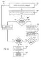
- FIG. 14depicts a method 1400 for activating a device according to one embodiment.
- the devicelistens for an activate code. Preferably, the device listens for the activate code periodically, though power drain is minimal and so continuous monitoring is preferred.
- the length fieldis compared to a stored length value in operation 1406 for determining whether the length field meets a predefined criterion. If the length field meets the predefined criterion, an address of the activate value is loaded in operation 1408 (if an address field is present) and the appropriate bits (mask value) of the mask field are compared to a stored activate value in operation 1410 . The comparison is terminated in operation 1412 upon comparing the final bit of the mask field as specified by the length field. An activate signal is generated in operation 1414 if the mask value matches the stored activate value. The activate signal can be used to activate additional circuitry in operation 1416 .
- RFID tag readersare placed near the store exits.
- the length fieldsare all set to zero so that all tags respond when in range of a reader. Accordingly, the readers continuously transmit zeros. If a tag responds, a security alarm is activated.
- a tagged itemIn a retail store, a tagged item is on a shelf and it is desired to reduce depletion of the battery as well as avoid unauthorized access to the tag.
- the length valueis set to some number greater than zero. Different tags may have different lengths or different activate codes.
- the length fieldand thus the mask field, are set small (e.g., mask value length ⁇ 16 bits) and no address offset to enable quick identification of RFID tags.
- the tagsare reprogrammed to have a mask field of many bits (e.g., mask value length >64 bits) and the address field is set to provide an offset of 12 bits.
- the resulting length fieldhas a value of 86 bits.
- the stored minimum length value of RFID tags in Group Ais set at 16 bits.
- the stored minimum length value of RFID tags in Group Bis set at 32 bits.
- An activate commandis sent having a length field value of 12 bits. No tags in Groups A or B respond.
- An activate commandis sent having a length field value of 20 bits.
- Tags in Group Aanalyze the activate code, while the tags in Group B do not.
- An activate commandis sent having a length field value of 40 bits.
- Tags in Groups A and Banalyze the activate code.
- a devicee.g., RFID tag
- a devicee.g., RFID tag
- Authorized users at various stages in the supply chainchange the activate code by submitting a password, etc. Now the device only responds to that particular activate command (as it otherwise remains in hibernate mode).
- the subsequent userreceives the activate code from the prior user, and possibly the password if the subsequent user does not already have it.
Landscapes
- Engineering & Computer Science (AREA)
- Theoretical Computer Science (AREA)
- Physics & Mathematics (AREA)
- General Physics & Mathematics (AREA)
- Computer Hardware Design (AREA)
- Microelectronics & Electronic Packaging (AREA)
- General Engineering & Computer Science (AREA)
- Business, Economics & Management (AREA)
- Electromagnetism (AREA)
- Economics (AREA)
- Computing Systems (AREA)
- Quality & Reliability (AREA)
- Computer Vision & Pattern Recognition (AREA)
- Development Economics (AREA)
- Artificial Intelligence (AREA)
- Entrepreneurship & Innovation (AREA)
- Human Resources & Organizations (AREA)
- Marketing (AREA)
- Operations Research (AREA)
- Computer Networks & Wireless Communication (AREA)
- Strategic Management (AREA)
- Tourism & Hospitality (AREA)
- General Business, Economics & Management (AREA)
- Near-Field Transmission Systems (AREA)
- Input Circuits Of Receivers And Coupling Of Receivers And Audio Equipment (AREA)
- Mobile Radio Communication Systems (AREA)
- Steroid Compounds (AREA)
- Surface Acoustic Wave Elements And Circuit Networks Thereof (AREA)
- Channel Selection Circuits, Automatic Tuning Circuits (AREA)
Abstract
Description
| TABLE 1 | |
| Barcode | RFID |
| Need line-of-sight to read | Identification without visual |
| contact | |
| Read only | Able to read/write |
| Only a barcode number | Able to store information in tag |
| Barcode number is fixed | Information can be renewed |
| anytime | |
| Category level tagging only-no unique | Unique item identification |
| item identifier | |
| Unable to read if barcode is damaged | Can withstand harsh |
| environment | |
| Use once | Reusable |
| Low cost | Higher cost |
| Less Flexibility | Higher Flexibility/Value |
- Class-1
- Identity tags (RF user programmable, maximum range 3 m)
- Lowest cost
- Class-2
- Memory tags (8 bits to 128 Mbits programmable at maximum 3 m range)
- Security & privacy protection
- Low cost
- Class-3
- Semi-Active tags
- Battery tags (256 bits to 64 Kb)
- Self-Powered Backscatter (internal clock, sensor interface support)
- 100 meter range
- Moderate cost
- Class-4
- Active tags
- Active transmission (permits tag-speaks-first operating modes)
- Up to 30,000 meter range
- Higher cost
- Class-1
- Clock spin-up or
synchronization section 302; - An interrupt304 to synchronize the start of a command with sufficient difference from “normal” commands (such as a timing violation in the forward communications protocol, or a “cluster” of bits that the device recognizes as an interrupt);
- An activate
code 306 to allow potentially selective, subset of all, or all-inclusive activation.
- Clock spin-up or
Claims (2)
Priority Applications (9)
| Application Number | Priority Date | Filing Date | Title |
|---|---|---|---|
| US11/186,666US8248211B2 (en) | 2005-07-20 | 2005-07-20 | Selective RF device activation |
| TW095125353ATWI437497B (en) | 2005-07-20 | 2006-07-11 | Selective rf device activation |
| ES06800180TES2360878T3 (en) | 2005-07-20 | 2006-07-19 | SELECTIVE ACTIVATION OF RF DEVICES. |
| PCT/US2006/028282WO2007012065A2 (en) | 2005-07-20 | 2006-07-19 | Selective rf device activation |
| EP06800180AEP1904949B1 (en) | 2005-07-20 | 2006-07-19 | Selective rf device activation |
| CN200680026302XACN101288085B (en) | 2005-07-20 | 2006-07-19 | Selective rf device activation |
| AT06800180TATE499659T1 (en) | 2005-07-20 | 2006-07-19 | SELECTIVE ACTIVATION OF RF DEVICES |
| DE602006020283TDE602006020283D1 (en) | 2005-07-20 | 2006-07-19 | SELECTIVE ACTIVATION OF RF DEVICES |
| US13/552,514US8674809B2 (en) | 2005-07-20 | 2012-07-18 | Selective RF device activation |
Applications Claiming Priority (1)
| Application Number | Priority Date | Filing Date | Title |
|---|---|---|---|
| US11/186,666US8248211B2 (en) | 2005-07-20 | 2005-07-20 | Selective RF device activation |
Related Child Applications (1)
| Application Number | Title | Priority Date | Filing Date |
|---|---|---|---|
| US13/552,514ContinuationUS8674809B2 (en) | 2005-07-20 | 2012-07-18 | Selective RF device activation |
Publications (2)
| Publication Number | Publication Date |
|---|---|
| US20070018794A1 US20070018794A1 (en) | 2007-01-25 |
| US8248211B2true US8248211B2 (en) | 2012-08-21 |
Family
ID=37546722
Family Applications (2)
| Application Number | Title | Priority Date | Filing Date |
|---|---|---|---|
| US11/186,666Active2031-05-05US8248211B2 (en) | 2005-07-20 | 2005-07-20 | Selective RF device activation |
| US13/552,514Expired - LifetimeUS8674809B2 (en) | 2005-07-20 | 2012-07-18 | Selective RF device activation |
Family Applications After (1)
| Application Number | Title | Priority Date | Filing Date |
|---|---|---|---|
| US13/552,514Expired - LifetimeUS8674809B2 (en) | 2005-07-20 | 2012-07-18 | Selective RF device activation |
Country Status (8)
| Country | Link |
|---|---|
| US (2) | US8248211B2 (en) |
| EP (1) | EP1904949B1 (en) |
| CN (1) | CN101288085B (en) |
| AT (1) | ATE499659T1 (en) |
| DE (1) | DE602006020283D1 (en) |
| ES (1) | ES2360878T3 (en) |
| TW (1) | TWI437497B (en) |
| WO (1) | WO2007012065A2 (en) |
Cited By (4)
| Publication number | Priority date | Publication date | Assignee | Title |
|---|---|---|---|---|
| US8674809B2 (en) | 2005-07-20 | 2014-03-18 | Intelleflex Corporation | Selective RF device activation |
| US9729201B2 (en)* | 2014-04-24 | 2017-08-08 | Empire Technology Development Llc | Broadcasting a message using modulated power |
| US20180276425A1 (en)* | 2017-03-22 | 2018-09-27 | Denso Wave Incorporated | Wireless tag passing determination apparatus |
| US20230412445A1 (en)* | 2022-04-08 | 2023-12-21 | Anno.Ai, Inc. | Passive RF Emitter Identification System and Methods |
Families Citing this family (24)
| Publication number | Priority date | Publication date | Assignee | Title |
|---|---|---|---|---|
| US7508249B2 (en)* | 2005-07-27 | 2009-03-24 | Analog Devices, Inc. | Distributed transistor structure for high linearity active CATV power splitter |
| US8174387B2 (en)* | 2007-01-24 | 2012-05-08 | United Security Applications Id, Inc. | Method of shipping and tracking inventory |
| DE102007038756A1 (en)* | 2007-08-16 | 2009-02-19 | Siemens Ag | Self-sustaining system e.g. self-sustaining sensor system, has waking-up device designed such that it produces wake-up signal for changing main system to active condition, where wake-up signal is acoustical and/or optical signal |
| KR100936607B1 (en)* | 2007-12-17 | 2010-01-13 | 한국전자통신연구원 | How to generate an activation code for the RFID tag |
| EP2283452B1 (en)* | 2008-04-22 | 2014-12-17 | Electronics and Telecommunications Research Institute | Rfid reader, rfid tag, and controlling method thereof |
| JP5217982B2 (en) | 2008-12-04 | 2013-06-19 | ソニー株式会社 | Information processing apparatus and method, and program |
| US8994508B2 (en)* | 2008-12-11 | 2015-03-31 | Intelleflex Corporation | Inclusive or exclusive RFID tag interrogation and query round |
| EP2581854B1 (en) | 2011-10-13 | 2019-06-26 | EM Microelectronic-Marin SA | Transponder with receiving means having a low electrical consumption in a listening mode |
| US20130154807A1 (en)* | 2011-12-19 | 2013-06-20 | Symbol Technologies, Inc. | Method and apparatus for detecting the activation of a call button using radio frequency identification |
| US9245158B2 (en) | 2012-04-05 | 2016-01-26 | Ricoh Co., Ltd. | Low power radio frequency communication |
| US9747538B2 (en)* | 2012-04-05 | 2017-08-29 | Ricoh Co., Ltd. | Low power radio frequency communication |
| WO2013170320A1 (en)* | 2012-05-18 | 2013-11-21 | Creata (Aust) Pty Limited | Exclusive information release authorisation system and method |
| KR101781371B1 (en)* | 2013-07-25 | 2017-09-25 | 삼성전자 주식회사 | Electronic apparatus and power controlling method thereof |
| US9978235B2 (en)* | 2015-07-02 | 2018-05-22 | Tyco Fire & Security Gmbh | Multi-technology transponder and system |
| FR3066287A1 (en)* | 2017-05-11 | 2018-11-16 | Orange | METHOD FOR MANAGING THE ELECTRIC CONSUMPTION OF A CONNECTED OBJECT |
| CN117596653A (en)* | 2017-12-01 | 2024-02-23 | 交互数字专利控股公司 | Network-initiated zero-energy paging method and device |
| US10417715B1 (en) | 2018-02-14 | 2019-09-17 | Hippo Technologies LLC | Computer architectures and associated methods for enabling real-time data determinations and distribution |
| CN108595953B (en)* | 2018-04-04 | 2020-05-19 | 东莞新辰智联科技有限公司 | Method for carrying out risk assessment on mobile phone application |
| CN109766980B (en)* | 2019-01-17 | 2022-05-06 | 卓捷创芯科技(深圳)有限公司 | Circuit and method for improving energy collection of passive radio frequency identification tag of temperature sensor |
| CN109561493B (en)* | 2019-01-21 | 2021-11-30 | 上海鸿研物流技术有限公司 | Terminal and awakening method thereof, and data reporting method and system of logistics system |
| CN112083690A (en)* | 2019-06-14 | 2020-12-15 | 调调(北京)科技有限公司 | Equipment, controller, and control method, device and system of equipment |
| CN112633023B (en)* | 2020-12-18 | 2022-03-01 | 中国电子科技集团公司第五十四研究所 | Decoding method and device for national military standard RFID (radio frequency identification) tag |
| CN113836952B (en)* | 2021-11-26 | 2022-03-29 | 广州智慧城市发展研究院 | Unique identifier UID matching method, device and equipment of electronic tag |
| CN115883455A (en)* | 2022-12-09 | 2023-03-31 | 苏州盛科通信股份有限公司 | Method and device for compressing routing information, electronic equipment and storage medium |
Citations (81)
| Publication number | Priority date | Publication date | Assignee | Title |
|---|---|---|---|---|
| US3689885A (en) | 1970-09-15 | 1972-09-05 | Transitag Corp | Inductively coupled passive responder and interrogator unit having multidimension electromagnetic field capabilities |
| US3890581A (en) | 1972-12-27 | 1975-06-17 | Rixon | Digital FM (FSK) modulator |
| US4004283A (en)* | 1974-10-30 | 1977-01-18 | Motorola, Inc. | Multiple interrupt microprocessor system |
| US4325146A (en) | 1979-12-20 | 1982-04-13 | Lennington John W | Non-synchronous object identification system |
| US4525713A (en) | 1983-03-01 | 1985-06-25 | Lockheed Electronics Co., Inc. | Electronic tag identification system |
| US4646090A (en) | 1983-08-12 | 1987-02-24 | Rca Corporation | Codeable identifying tag and method of identification thereof |
| US4730188A (en) | 1984-02-15 | 1988-03-08 | Identification Devices, Inc. | Identification system |
| US4839642A (en) | 1985-01-22 | 1989-06-13 | Northern Illinois Gas Company | Data transmission system with data verification |
| US4879756A (en) | 1986-09-22 | 1989-11-07 | Stevens John K | Radio broadcast communication systems |
| US4928275A (en) | 1989-05-26 | 1990-05-22 | Northern Telecom Limited | Synchronization of asynchronous data signals |
| US4937586A (en) | 1986-09-22 | 1990-06-26 | Stevens John K | Radio broadcast communication systems with multiple loop antennas |
| US4955038A (en) | 1988-12-09 | 1990-09-04 | Dallas Semiconductor Corporation | Low-power RF receiver |
| US5028918A (en) | 1989-12-18 | 1991-07-02 | Dairy Equipment Company | Identification transponder circuit |
| US5089813A (en)* | 1989-07-19 | 1992-02-18 | Motorola, Inc. | Method of super battery saving in a selective call receiver |
| US5109221A (en) | 1987-05-21 | 1992-04-28 | Trw Inc. | Remote control system for door locks |
| US5245332A (en) | 1988-06-22 | 1993-09-14 | Iedsco Oy | Programmable memory for an encoding system |
| US5305008A (en) | 1991-08-12 | 1994-04-19 | Integrated Silicon Design Pty. Ltd. | Transponder system |
| US5345231A (en) | 1990-08-23 | 1994-09-06 | Mikron Gesellschaft Fur Integrierte Mikroelectronik Mbh | Contactless inductive data-transmission system |
| US5410315A (en) | 1992-12-08 | 1995-04-25 | Texas Instruments Incorporated | Group-addressable transponder arrangement |
| US5489908A (en) | 1994-07-27 | 1996-02-06 | Texas Instruments Deutschland Gmbh | Apparatus and method for identifying multiple transponders |
| US5491482A (en) | 1992-12-29 | 1996-02-13 | David Sarnoff Research Center, Inc. | Electronic system and method for remote identification of coded articles and the like |
| EP0702323A2 (en) | 1994-09-09 | 1996-03-20 | International Business Machines Corporation | System and method for radio frequency tag group select |
| US5521601A (en) | 1995-04-21 | 1996-05-28 | International Business Machines Corporation | Power-efficient technique for multiple tag discrimination |
| US5525992A (en) | 1994-11-14 | 1996-06-11 | Texas Instruments Deutschland Gmbh | Method and system for conserving power in a recognition system |
| US5530702A (en) | 1994-05-31 | 1996-06-25 | Ludwig Kipp | System for storage and communication of information |
| US5548291A (en) | 1992-11-25 | 1996-08-20 | Texas Instruments Deutschland Gmbh | Read/write transponder arrangement and method of communication |
| US5550536A (en) | 1994-08-17 | 1996-08-27 | Texas Instruments Deutschland Gmbh | Circuit frequency following technique transponder resonant |
| US5606313A (en) | 1993-12-10 | 1997-02-25 | Motorola, Inc. | Low power addressable data communication device and method |
| US5621412A (en) | 1994-04-26 | 1997-04-15 | Texas Instruments Incorporated | Multi-stage transponder wake-up, method and structure |
| US5684828A (en) | 1988-12-09 | 1997-11-04 | Dallas Semiconductor Corp. | Wireless data module with two separate transmitter control outputs |
| US5774064A (en) | 1987-05-21 | 1998-06-30 | Trw Inc. | Remote control system for door locks |
| US5838257A (en) | 1996-05-24 | 1998-11-17 | Trw Inc. | Keyless vehicle entry system employing portable transceiver having low power consumption |
| US5856788A (en) | 1996-03-12 | 1999-01-05 | Single Chips Systems Corp. | Method and apparatus for radiofrequency identification tags |
| US5887176A (en) | 1996-06-28 | 1999-03-23 | Randtec, Inc. | Method and system for remote monitoring and tracking of inventory |
| US6104333A (en) | 1996-12-19 | 2000-08-15 | Micron Technology, Inc. | Methods of processing wireless communication, methods of processing radio frequency communication, and related systems |
| US6130602A (en) | 1996-05-13 | 2000-10-10 | Micron Technology, Inc. | Radio frequency data communications device |
| US6130603A (en) | 1994-06-13 | 2000-10-10 | Ers International, Inc. | Low-powered RF-linked price display system |
| US6150921A (en) | 1996-10-17 | 2000-11-21 | Pinpoint Corporation | Article tracking system |
| US6172596B1 (en) | 1994-09-09 | 2001-01-09 | Intermec Ip Corp. | System method and apparatus for identifying and communicating with a plurality of types of radio frequency communication devices |
| US6177858B1 (en) | 1995-12-01 | 2001-01-23 | Pierre Raimbault | Method for remotely interrogating tags, and station and tag implementing said method |
| US6239690B1 (en) | 1997-11-12 | 2001-05-29 | U.S. Philips Corporation | Battery economizing in a communications system |
| US6249212B1 (en) | 1994-10-05 | 2001-06-19 | Avid Marketing, Inc. | Universal electronic identification tag |
| US6310558B1 (en) | 1994-07-15 | 2001-10-30 | Nec Corporation | Selective calling system and selective calling receiver |
| US20010050580A1 (en) | 1996-05-13 | 2001-12-13 | O'toole James E. | Radio frequency data communications device |
| US6333690B1 (en) | 1995-03-29 | 2001-12-25 | Medical Tracking Systems | Wide area multipurpose tracking system |
| US6342830B1 (en) | 1998-09-10 | 2002-01-29 | Xerox Corporation | Controlled shielding of electronic tags |
| US6351215B2 (en) | 1998-06-02 | 2002-02-26 | Rf Code, Inc. | Monitoring antenna system |
| US20020024422A1 (en) | 2000-06-12 | 2002-02-28 | Turner Christopher Gordon Gervase | Reading protocol for transponders of electronic identification system |
| US6353406B1 (en) | 1996-10-17 | 2002-03-05 | R.F. Technologies, Inc. | Dual mode tracking system |
| US6362738B1 (en) | 1998-04-16 | 2002-03-26 | Motorola, Inc. | Reader for use in a radio frequency identification system and method thereof |
| US6388575B1 (en) | 1999-11-05 | 2002-05-14 | Industrial Technology, Inc. | Addressable underground marker |
| US20020063622A1 (en) | 2000-11-29 | 2002-05-30 | Ludwig Kipp | Method and system for communicating with and tracking RFID transponders |
| US6411199B1 (en) | 1998-08-21 | 2002-06-25 | Keri Systems, Inc. | Radio frequency identification system |
| US6441719B1 (en)* | 1998-02-13 | 2002-08-27 | Philip Y. W. Tsui | Remote signaling device for a rolling code security system |
| US20020126005A1 (en) | 2000-07-26 | 2002-09-12 | Hardman Gordon E. | Electronic tire management system |
| US6452980B1 (en) | 2000-01-10 | 2002-09-17 | Sarnoff Corporation | Encoding/decoding system for coherent signal interference reduction |
| US6469618B1 (en) | 1998-02-04 | 2002-10-22 | Stmicroelectronics S.A. | Method for the identification of electronic cards presented in an investigation zone |
| US20020175806A1 (en) | 2001-05-25 | 2002-11-28 | Marneweck Willem J. | Electronic tag binary selection method |
| US6535109B1 (en) | 1998-12-01 | 2003-03-18 | Texas Instruments Sensors And Controls, Inc. | System and method for communicating with multiple transponders |
| US20030104848A1 (en) | 2001-11-30 | 2003-06-05 | Raj Brideglall | RFID device, system and method of operation including a hybrid backscatter-based RFID tag protocol compatible with RFID, bluetooth and/or IEEE 802.11x infrastructure |
| US20030128100A1 (en) | 2001-11-26 | 2003-07-10 | Aero-Vision Technologies, Inc. | System and method for monitoring individuals and objects associated with wireless identification tags |
| US6593845B1 (en) | 1998-01-09 | 2003-07-15 | Intermac Ip Corp. | Active RF tag with wake-up circuit to prolong battery life |
| US6603391B1 (en) | 1999-03-09 | 2003-08-05 | Micron Technology, Inc. | Phase shifters, interrogators, methods of shifting a phase angle of a signal, and methods of operating an interrogator |
| US20030149526A1 (en) | 2001-10-29 | 2003-08-07 | Zhou Peter Y | Systems and methods for monitoring and tracking related U.S. patent applications |
| US6617963B1 (en) | 1999-02-26 | 2003-09-09 | Sri International | Event-recording devices with identification codes |
| US6661336B1 (en) | 1997-05-14 | 2003-12-09 | Btg International Limited | Enhanced identification system |
| US6690264B2 (en) | 2001-01-23 | 2004-02-10 | Single Chip Systems Corporation | Selective cloaking circuit for use in a radiofrequency identification and method of cloaking RFID tags |
| US6693511B1 (en) | 1999-09-24 | 2004-02-17 | Ge Interlogix, Inc. | System and method for communicating with dormant radio frequency identification tags |
| US6696879B1 (en) | 1996-05-13 | 2004-02-24 | Micron Technology, Inc. | Radio frequency data communications device |
| US20040046642A1 (en) | 2002-09-05 | 2004-03-11 | Honeywell International Inc. | Protocol for addressing groups of RFID tags |
| US6765484B2 (en) | 2000-09-07 | 2004-07-20 | Savi Technology, Inc. | Method and apparatus for supplying commands to a tag |
| US6765476B2 (en) | 2001-03-09 | 2004-07-20 | Battelle Memorial Institute Kl-53 | Multi-level RF identification system |
| US20040140884A1 (en) | 1999-10-27 | 2004-07-22 | Microchip Technology Inc. | Anticollision protocol with fast read request and additional schemes for reading multiple transponders in an RFID system |
| US20040160306A1 (en) | 2003-02-03 | 2004-08-19 | Stilp Louis A. | Device enrollment in a security system |
| US20040160309A1 (en) | 2003-02-03 | 2004-08-19 | Stilp Louis A. | Communications control in a security system |
| US20040223481A1 (en) | 2003-05-08 | 2004-11-11 | Ari Juels | Method and apparatus for selective blocking of radio frequency identification devices |
| US6831548B1 (en) | 1998-08-17 | 2004-12-14 | Koninklijke Philips Electronics N.V. | Data carrier with means for reducing the power consumption upon reception of data |
| US20050052283A1 (en) | 2003-09-09 | 2005-03-10 | Collins Timothy J. | Method and apparatus for multiple frequency RFID tag architecture |
| US20050057368A1 (en) | 2003-09-17 | 2005-03-17 | Government Of The United States Of America As Represented By The Secretary Of The Navy. | Continuous wave (CW) - fixed multiple frequency triggered, radio frequency identification (RFID) tag and system and method employing same |
| US20050077349A1 (en) | 2000-03-07 | 2005-04-14 | American Express Travel Related Services Company, Inc. | Method and system for facilitating a transaction using a transponder |
| US7375637B2 (en) | 2005-04-21 | 2008-05-20 | University Of Pittsburgh Of The Commonwealth Of Pennsylvania | Methods and apparatus for reducing power consumption of an active transponder |
Family Cites Families (7)
| Publication number | Priority date | Publication date | Assignee | Title |
|---|---|---|---|---|
| US5266925A (en)* | 1991-09-30 | 1993-11-30 | Westinghouse Electric Corp. | Electronic identification tag interrogation method |
| US5365551A (en)* | 1992-12-15 | 1994-11-15 | Micron Technology, Inc. | Data communication transceiver using identification protocol |
| US6169483B1 (en)* | 1999-05-04 | 2001-01-02 | Sensormatic Electronics Corporation | Self-checkout/self-check-in RFID and electronics article surveillance system |
| US6486783B1 (en)* | 2000-09-19 | 2002-11-26 | Moore North America, Inc. | RFID composite for mounting on or adjacent metal objects |
| US7397773B2 (en)* | 2002-10-22 | 2008-07-08 | Qualcomm Incorporated | GSM cell broadcast SMS message transmission in CDMA communication systems |
| DE602004027532D1 (en)* | 2003-12-09 | 2010-07-15 | Intelleflex Corp | BATTERY ACTIVATION CIRCUIT |
| US8248211B2 (en) | 2005-07-20 | 2012-08-21 | Intelleflex Corporation | Selective RF device activation |
- 2005
- 2005-07-20USUS11/186,666patent/US8248211B2/enactiveActive
- 2006
- 2006-07-11TWTW095125353Apatent/TWI437497B/ennot_activeIP Right Cessation
- 2006-07-19CNCN200680026302XApatent/CN101288085B/ennot_activeExpired - Fee Related
- 2006-07-19ATAT06800180Tpatent/ATE499659T1/ennot_activeIP Right Cessation
- 2006-07-19DEDE602006020283Tpatent/DE602006020283D1/enactiveActive
- 2006-07-19WOPCT/US2006/028282patent/WO2007012065A2/enactiveSearch and Examination
- 2006-07-19ESES06800180Tpatent/ES2360878T3/enactiveActive
- 2006-07-19EPEP06800180Apatent/EP1904949B1/ennot_activeNot-in-force
- 2012
- 2012-07-18USUS13/552,514patent/US8674809B2/ennot_activeExpired - Lifetime
Patent Citations (102)
| Publication number | Priority date | Publication date | Assignee | Title |
|---|---|---|---|---|
| US3689885A (en) | 1970-09-15 | 1972-09-05 | Transitag Corp | Inductively coupled passive responder and interrogator unit having multidimension electromagnetic field capabilities |
| US3890581A (en) | 1972-12-27 | 1975-06-17 | Rixon | Digital FM (FSK) modulator |
| US4004283A (en)* | 1974-10-30 | 1977-01-18 | Motorola, Inc. | Multiple interrupt microprocessor system |
| US4325146A (en) | 1979-12-20 | 1982-04-13 | Lennington John W | Non-synchronous object identification system |
| US4525713A (en) | 1983-03-01 | 1985-06-25 | Lockheed Electronics Co., Inc. | Electronic tag identification system |
| US4646090A (en) | 1983-08-12 | 1987-02-24 | Rca Corporation | Codeable identifying tag and method of identification thereof |
| US4730188A (en) | 1984-02-15 | 1988-03-08 | Identification Devices, Inc. | Identification system |
| US5041826A (en) | 1984-02-15 | 1991-08-20 | Destron/Idi Inc. | Identification system |
| US5166676A (en) | 1984-02-15 | 1992-11-24 | Destron/Idi, Inc. | Identification system |
| US4839642A (en) | 1985-01-22 | 1989-06-13 | Northern Illinois Gas Company | Data transmission system with data verification |
| US4879756A (en) | 1986-09-22 | 1989-11-07 | Stevens John K | Radio broadcast communication systems |
| US4937586A (en) | 1986-09-22 | 1990-06-26 | Stevens John K | Radio broadcast communication systems with multiple loop antennas |
| US5109221A (en) | 1987-05-21 | 1992-04-28 | Trw Inc. | Remote control system for door locks |
| US5774064A (en) | 1987-05-21 | 1998-06-30 | Trw Inc. | Remote control system for door locks |
| US5245332A (en) | 1988-06-22 | 1993-09-14 | Iedsco Oy | Programmable memory for an encoding system |
| US5684828A (en) | 1988-12-09 | 1997-11-04 | Dallas Semiconductor Corp. | Wireless data module with two separate transmitter control outputs |
| US4955038A (en) | 1988-12-09 | 1990-09-04 | Dallas Semiconductor Corporation | Low-power RF receiver |
| US4928275A (en) | 1989-05-26 | 1990-05-22 | Northern Telecom Limited | Synchronization of asynchronous data signals |
| US5089813A (en)* | 1989-07-19 | 1992-02-18 | Motorola, Inc. | Method of super battery saving in a selective call receiver |
| US5028918A (en) | 1989-12-18 | 1991-07-02 | Dairy Equipment Company | Identification transponder circuit |
| US5345231A (en) | 1990-08-23 | 1994-09-06 | Mikron Gesellschaft Fur Integrierte Mikroelectronik Mbh | Contactless inductive data-transmission system |
| US5305008A (en) | 1991-08-12 | 1994-04-19 | Integrated Silicon Design Pty. Ltd. | Transponder system |
| US5548291A (en) | 1992-11-25 | 1996-08-20 | Texas Instruments Deutschland Gmbh | Read/write transponder arrangement and method of communication |
| US5410315A (en) | 1992-12-08 | 1995-04-25 | Texas Instruments Incorporated | Group-addressable transponder arrangement |
| US5502445A (en) | 1992-12-29 | 1996-03-26 | David Sarnoff Research Center, Inc. | System and method for remote identification of coded articles and the like |
| US5491482A (en) | 1992-12-29 | 1996-02-13 | David Sarnoff Research Center, Inc. | Electronic system and method for remote identification of coded articles and the like |
| US5606313A (en) | 1993-12-10 | 1997-02-25 | Motorola, Inc. | Low power addressable data communication device and method |
| US5621412A (en) | 1994-04-26 | 1997-04-15 | Texas Instruments Incorporated | Multi-stage transponder wake-up, method and structure |
| US5530702A (en) | 1994-05-31 | 1996-06-25 | Ludwig Kipp | System for storage and communication of information |
| US6130603A (en) | 1994-06-13 | 2000-10-10 | Ers International, Inc. | Low-powered RF-linked price display system |
| US6310558B1 (en) | 1994-07-15 | 2001-10-30 | Nec Corporation | Selective calling system and selective calling receiver |
| US5489908A (en) | 1994-07-27 | 1996-02-06 | Texas Instruments Deutschland Gmbh | Apparatus and method for identifying multiple transponders |
| US5550536A (en) | 1994-08-17 | 1996-08-27 | Texas Instruments Deutschland Gmbh | Circuit frequency following technique transponder resonant |
| EP0702323A2 (en) | 1994-09-09 | 1996-03-20 | International Business Machines Corporation | System and method for radio frequency tag group select |
| US5673037A (en) | 1994-09-09 | 1997-09-30 | International Business Machines Corporation | System and method for radio frequency tag group select |
| US6172596B1 (en) | 1994-09-09 | 2001-01-09 | Intermec Ip Corp. | System method and apparatus for identifying and communicating with a plurality of types of radio frequency communication devices |
| US6249212B1 (en) | 1994-10-05 | 2001-06-19 | Avid Marketing, Inc. | Universal electronic identification tag |
| US5525992A (en) | 1994-11-14 | 1996-06-11 | Texas Instruments Deutschland Gmbh | Method and system for conserving power in a recognition system |
| US6653937B2 (en) | 1995-03-29 | 2003-11-25 | Medical Tracking Systems, Inc. | Wide area multipurpose tracking system |
| US20020109597A1 (en) | 1995-03-29 | 2002-08-15 | Medical Tracking Systems, Inc. | Wide area multipurpose tracking system |
| US6333690B1 (en) | 1995-03-29 | 2001-12-25 | Medical Tracking Systems | Wide area multipurpose tracking system |
| US5521601A (en) | 1995-04-21 | 1996-05-28 | International Business Machines Corporation | Power-efficient technique for multiple tag discrimination |
| US6177858B1 (en) | 1995-12-01 | 2001-01-23 | Pierre Raimbault | Method for remotely interrogating tags, and station and tag implementing said method |
| US5856788A (en) | 1996-03-12 | 1999-01-05 | Single Chips Systems Corp. | Method and apparatus for radiofrequency identification tags |
| US20010050580A1 (en) | 1996-05-13 | 2001-12-13 | O'toole James E. | Radio frequency data communications device |
| US6774685B2 (en) | 1996-05-13 | 2004-08-10 | Micron Technology, Inc. | Radio frequency data communications device |
| US6600428B1 (en) | 1996-05-13 | 2003-07-29 | Micron Technology, Inc. | Radio frequency data communications device |
| US6278698B1 (en) | 1996-05-13 | 2001-08-21 | Micron Technology, Inc. | Radio frequency data communications device |
| US6696879B1 (en) | 1996-05-13 | 2004-02-24 | Micron Technology, Inc. | Radio frequency data communications device |
| US6130602A (en) | 1996-05-13 | 2000-10-10 | Micron Technology, Inc. | Radio frequency data communications device |
| US6466634B1 (en) | 1996-05-13 | 2002-10-15 | Micron Technology, Inc. | Radio frequency data communications device |
| US6337634B1 (en) | 1996-05-13 | 2002-01-08 | Micron Technology, Inc. | Radio frequency data communications device |
| US6721289B1 (en) | 1996-05-13 | 2004-04-13 | Micron Technology, Inc. | Radio frequency data communications device |
| US6735183B2 (en) | 1996-05-13 | 2004-05-11 | Micron Technology, Inc. | Radio frequency data communications device |
| US20040201457A1 (en) | 1996-05-13 | 2004-10-14 | O'toole James E. | Radio frequency data communications device |
| US6771613B1 (en) | 1996-05-13 | 2004-08-03 | Micron Technology, Inc. | Radio frequency data communications device |
| US5838257A (en) | 1996-05-24 | 1998-11-17 | Trw Inc. | Keyless vehicle entry system employing portable transceiver having low power consumption |
| US5887176A (en) | 1996-06-28 | 1999-03-23 | Randtec, Inc. | Method and system for remote monitoring and tracking of inventory |
| US6150921A (en) | 1996-10-17 | 2000-11-21 | Pinpoint Corporation | Article tracking system |
| US6353406B1 (en) | 1996-10-17 | 2002-03-05 | R.F. Technologies, Inc. | Dual mode tracking system |
| US6265963B1 (en) | 1996-12-19 | 2001-07-24 | Micron Technology, Inc. | Methods of processing wireless communication, methods of processing radio frequency communication, and related systems |
| US6104333A (en) | 1996-12-19 | 2000-08-15 | Micron Technology, Inc. | Methods of processing wireless communication, methods of processing radio frequency communication, and related systems |
| US6661336B1 (en) | 1997-05-14 | 2003-12-09 | Btg International Limited | Enhanced identification system |
| US6239690B1 (en) | 1997-11-12 | 2001-05-29 | U.S. Philips Corporation | Battery economizing in a communications system |
| US6593845B1 (en) | 1998-01-09 | 2003-07-15 | Intermac Ip Corp. | Active RF tag with wake-up circuit to prolong battery life |
| US6469618B1 (en) | 1998-02-04 | 2002-10-22 | Stmicroelectronics S.A. | Method for the identification of electronic cards presented in an investigation zone |
| US6441719B1 (en)* | 1998-02-13 | 2002-08-27 | Philip Y. W. Tsui | Remote signaling device for a rolling code security system |
| US6362738B1 (en) | 1998-04-16 | 2002-03-26 | Motorola, Inc. | Reader for use in a radio frequency identification system and method thereof |
| US6351215B2 (en) | 1998-06-02 | 2002-02-26 | Rf Code, Inc. | Monitoring antenna system |
| US6831548B1 (en) | 1998-08-17 | 2004-12-14 | Koninklijke Philips Electronics N.V. | Data carrier with means for reducing the power consumption upon reception of data |
| US6411199B1 (en) | 1998-08-21 | 2002-06-25 | Keri Systems, Inc. | Radio frequency identification system |
| US6611198B1 (en) | 1998-08-21 | 2003-08-26 | Keri Systems Incorporated | Electronic reader for reading a special characteristic of an object |
| US6342830B1 (en) | 1998-09-10 | 2002-01-29 | Xerox Corporation | Controlled shielding of electronic tags |
| US6535109B1 (en) | 1998-12-01 | 2003-03-18 | Texas Instruments Sensors And Controls, Inc. | System and method for communicating with multiple transponders |
| US6617963B1 (en) | 1999-02-26 | 2003-09-09 | Sri International | Event-recording devices with identification codes |
| US20040027240A1 (en) | 1999-03-09 | 2004-02-12 | Roy Greeff | Interrogators, methods of operating a coherent interrogator, backscatter communication methods, interrogation methods, and signal processing methods |
| US6603391B1 (en) | 1999-03-09 | 2003-08-05 | Micron Technology, Inc. | Phase shifters, interrogators, methods of shifting a phase angle of a signal, and methods of operating an interrogator |
| US6693511B1 (en) | 1999-09-24 | 2004-02-17 | Ge Interlogix, Inc. | System and method for communicating with dormant radio frequency identification tags |
| US20040140884A1 (en) | 1999-10-27 | 2004-07-22 | Microchip Technology Inc. | Anticollision protocol with fast read request and additional schemes for reading multiple transponders in an RFID system |
| US6388575B1 (en) | 1999-11-05 | 2002-05-14 | Industrial Technology, Inc. | Addressable underground marker |
| US6452980B1 (en) | 2000-01-10 | 2002-09-17 | Sarnoff Corporation | Encoding/decoding system for coherent signal interference reduction |
| US20050077349A1 (en) | 2000-03-07 | 2005-04-14 | American Express Travel Related Services Company, Inc. | Method and system for facilitating a transaction using a transponder |
| US20020024422A1 (en) | 2000-06-12 | 2002-02-28 | Turner Christopher Gordon Gervase | Reading protocol for transponders of electronic identification system |
| US6630885B2 (en) | 2000-07-26 | 2003-10-07 | Bridgestone/Firestone North American Tire, Llc | Electronic tire management system |
| US20020126005A1 (en) | 2000-07-26 | 2002-09-12 | Hardman Gordon E. | Electronic tire management system |
| US20040017291A1 (en) | 2000-07-26 | 2004-01-29 | Hardman Gordon E. | Electronic tire management system |
| US6765484B2 (en) | 2000-09-07 | 2004-07-20 | Savi Technology, Inc. | Method and apparatus for supplying commands to a tag |
| US20020175805A9 (en) | 2000-11-29 | 2002-11-28 | Ludwig Kipp | Method and system for communicating with and tracking RFID transponders |
| US20020063622A1 (en) | 2000-11-29 | 2002-05-30 | Ludwig Kipp | Method and system for communicating with and tracking RFID transponders |
| US6690264B2 (en) | 2001-01-23 | 2004-02-10 | Single Chip Systems Corporation | Selective cloaking circuit for use in a radiofrequency identification and method of cloaking RFID tags |
| US6765476B2 (en) | 2001-03-09 | 2004-07-20 | Battelle Memorial Institute Kl-53 | Multi-level RF identification system |
| US20020175806A1 (en) | 2001-05-25 | 2002-11-28 | Marneweck Willem J. | Electronic tag binary selection method |
| US20030149526A1 (en) | 2001-10-29 | 2003-08-07 | Zhou Peter Y | Systems and methods for monitoring and tracking related U.S. patent applications |
| US20030128100A1 (en) | 2001-11-26 | 2003-07-10 | Aero-Vision Technologies, Inc. | System and method for monitoring individuals and objects associated with wireless identification tags |
| US20030104848A1 (en) | 2001-11-30 | 2003-06-05 | Raj Brideglall | RFID device, system and method of operation including a hybrid backscatter-based RFID tag protocol compatible with RFID, bluetooth and/or IEEE 802.11x infrastructure |
| US20040046642A1 (en) | 2002-09-05 | 2004-03-11 | Honeywell International Inc. | Protocol for addressing groups of RFID tags |
| US20040160306A1 (en) | 2003-02-03 | 2004-08-19 | Stilp Louis A. | Device enrollment in a security system |
| US20040160309A1 (en) | 2003-02-03 | 2004-08-19 | Stilp Louis A. | Communications control in a security system |
| US20040223481A1 (en) | 2003-05-08 | 2004-11-11 | Ari Juels | Method and apparatus for selective blocking of radio frequency identification devices |
| US20050052283A1 (en) | 2003-09-09 | 2005-03-10 | Collins Timothy J. | Method and apparatus for multiple frequency RFID tag architecture |
| US20050057368A1 (en) | 2003-09-17 | 2005-03-17 | Government Of The United States Of America As Represented By The Secretary Of The Navy. | Continuous wave (CW) - fixed multiple frequency triggered, radio frequency identification (RFID) tag and system and method employing same |
| US7375637B2 (en) | 2005-04-21 | 2008-05-20 | University Of Pittsburgh Of The Commonwealth Of Pennsylvania | Methods and apparatus for reducing power consumption of an active transponder |
Non-Patent Citations (5)
| Title |
|---|
| Chinese Office Action from application No. 200680026302.X dated Jul. 22, 2011 (no translation). |
| Chinese Office Action Summary from application No. 200680026302.X dated Feb. 23, 2011 (no translation). |
| European Office Action Summary from application No. 06800180.9 mailed on Oct. 23, 2009. |
| PCT Search Report from application No. PCT/US2006/028282 which was mailed on Jan. 12, 2007. |
| U.S. Appl. No. 60/673,715, filed Apr. 21, 2005. |
Cited By (6)
| Publication number | Priority date | Publication date | Assignee | Title |
|---|---|---|---|---|
| US8674809B2 (en) | 2005-07-20 | 2014-03-18 | Intelleflex Corporation | Selective RF device activation |
| US9729201B2 (en)* | 2014-04-24 | 2017-08-08 | Empire Technology Development Llc | Broadcasting a message using modulated power |
| US20180276425A1 (en)* | 2017-03-22 | 2018-09-27 | Denso Wave Incorporated | Wireless tag passing determination apparatus |
| US10503938B2 (en)* | 2017-03-22 | 2019-12-10 | Denso Wave Incorporated | Wireless tag passing determination apparatus |
| US20230412445A1 (en)* | 2022-04-08 | 2023-12-21 | Anno.Ai, Inc. | Passive RF Emitter Identification System and Methods |
| US12355606B2 (en)* | 2022-04-08 | 2025-07-08 | Anno.Ai, Inc. | Passive RF emitter identification system and methods |
Also Published As
| Publication number | Publication date |
|---|---|
| ES2360878T3 (en) | 2011-06-09 |
| US20070018794A1 (en) | 2007-01-25 |
| DE602006020283D1 (en) | 2011-04-07 |
| ATE499659T1 (en) | 2011-03-15 |
| WO2007012065A2 (en) | 2007-01-25 |
| WO2007012065A3 (en) | 2007-04-05 |
| EP1904949B1 (en) | 2011-02-23 |
| US20120319824A1 (en) | 2012-12-20 |
| US8674809B2 (en) | 2014-03-18 |
| CN101288085B (en) | 2012-02-22 |
| EP1904949A2 (en) | 2008-04-02 |
| TWI437497B (en) | 2014-05-11 |
| TW200710737A (en) | 2007-03-16 |
| CN101288085A (en) | 2008-10-15 |
Similar Documents
| Publication | Publication Date | Title |
|---|---|---|
| US8674809B2 (en) | Selective RF device activation | |
| US7604178B2 (en) | Smart tag activation | |
| US7612652B2 (en) | Battery activation circuit | |
| EP1904948B1 (en) | Ramped interrogation power levels | |
| EP1362320B1 (en) | Radio frequency identification architecture | |
| US5502445A (en) | System and method for remote identification of coded articles and the like | |
| US8570172B2 (en) | RFID system with distributed transmitters | |
| US8098159B2 (en) | RF device comparing DAC output to incoming signal for selectively performing an action | |
| WO2007078521A2 (en) | Clock-free activation circuit | |
| WO2007078520A2 (en) | Clock generation circuit | |
| JP2940562B2 (en) | Electronic system and method for remote identification of coded articles and the like | |
| WO2007136690A2 (en) | Circuitry for adaptively generating and using a reference voltage | |
| TWI270822B (en) | Battery activation circuit |
Legal Events
| Date | Code | Title | Description |
|---|---|---|---|
| AS | Assignment | Owner name:INTELLEFLEX CORPORATION, CALIFORNIA Free format text:ASSIGNMENT OF ASSIGNORS INTEREST;ASSIGNORS:BARES, WILLIAM HENRY;PALEY, DANIEL NOAH;SCHLICHT, LAUREN MARIE;REEL/FRAME:017847/0440 Effective date:20050718 | |
| AS | Assignment | Owner name:VENTURE LENDING & LEASING IV, INC. AS AGENT, CALIF Free format text:SECURITY INTEREST;ASSIGNOR:INTELLEFLEX CORPORATION;REEL/FRAME:020955/0628 Effective date:20080422 Owner name:VENTURE LENDING & LEASING IV, INC. AS AGENT,CALIFO Free format text:SECURITY INTEREST;ASSIGNOR:INTELLEFLEX CORPORATION;REEL/FRAME:020955/0628 Effective date:20080422 | |
| AS | Assignment | Owner name:VENTURE LENDING & LEASING V, INC., AS AGENT, CALIF Free format text:SECURITY AGREEMENT;ASSIGNOR:INTELLEFLEX CORPORATION;REEL/FRAME:020960/0279 Effective date:20080422 Owner name:VENTURE LENDING & LEASING V, INC., AS AGENT,CALIFO Free format text:SECURITY AGREEMENT;ASSIGNOR:INTELLEFLEX CORPORATION;REEL/FRAME:020960/0279 Effective date:20080422 | |
| STCF | Information on status: patent grant | Free format text:PATENTED CASE | |
| FPAY | Fee payment | Year of fee payment:4 | |
| AS | Assignment | Owner name:ZEST LABS, INC., CALIFORNIA Free format text:CHANGE OF NAME;ASSIGNOR:INTELLEFLEX CORPORATION;REEL/FRAME:041678/0799 Effective date:20161027 | |
| MAFP | Maintenance fee payment | Free format text:PAYMENT OF MAINTENANCE FEE, 8TH YEAR, LARGE ENTITY (ORIGINAL EVENT CODE: M1552); ENTITY STATUS OF PATENT OWNER: LARGE ENTITY Year of fee payment:8 | |
| FEPP | Fee payment procedure | Free format text:MAINTENANCE FEE REMINDER MAILED (ORIGINAL EVENT CODE: REM.); ENTITY STATUS OF PATENT OWNER: LARGE ENTITY | |
| FEPP | Fee payment procedure | Free format text:11.5 YR SURCHARGE- LATE PMT W/IN 6 MO, LARGE ENTITY (ORIGINAL EVENT CODE: M1556); ENTITY STATUS OF PATENT OWNER: LARGE ENTITY | |
| MAFP | Maintenance fee payment | Free format text:PAYMENT OF MAINTENANCE FEE, 12TH YEAR, LARGE ENTITY (ORIGINAL EVENT CODE: M1553); ENTITY STATUS OF PATENT OWNER: LARGE ENTITY Year of fee payment:12 |