US8247875B2 - Fabrication method of semiconductor device - Google Patents
Fabrication method of semiconductor deviceDownload PDFInfo
- Publication number
- US8247875B2 US8247875B2US12/942,503US94250310AUS8247875B2US 8247875 B2US8247875 B2US 8247875B2US 94250310 AUS94250310 AUS 94250310AUS 8247875 B2US8247875 B2US 8247875B2
- Authority
- US
- United States
- Prior art keywords
- source
- drain regions
- type
- gate electrode
- regions
- Prior art date
- Legal status (The legal status is an assumption and is not a legal conclusion. Google has not performed a legal analysis and makes no representation as to the accuracy of the status listed.)
- Expired - Fee Related, expires
Links
- 239000004065semiconductorSubstances0.000titleclaimsabstractdescription22
- 238000000034methodMethods0.000titleabstractdescription57
- 238000004519manufacturing processMethods0.000titleabstractdescription37
- 229910052710siliconInorganic materials0.000claimsabstractdescription45
- 239000010703siliconSubstances0.000claimsabstractdescription45
- 229910052751metalInorganic materials0.000claimsabstractdescription22
- 239000002184metalSubstances0.000claimsabstractdescription22
- 229910021332silicideInorganic materials0.000claimsabstractdescription18
- FVBUAEGBCNSCDD-UHFFFAOYSA-Nsilicide(4-)Chemical compound[Si-4]FVBUAEGBCNSCDD-UHFFFAOYSA-N0.000claimsabstractdescription18
- 230000001747exhibiting effectEffects0.000claimsabstractdescription6
- RUFLMLWJRZAWLJ-UHFFFAOYSA-Nnickel silicideChemical compound[Ni]=[Si]=[Ni]RUFLMLWJRZAWLJ-UHFFFAOYSA-N0.000claimsdescription30
- 229910021334nickel silicideInorganic materials0.000claimsdescription28
- 239000000758substrateSubstances0.000claimsdescription20
- ZOXJGFHDIHLPTG-UHFFFAOYSA-NBoronChemical group[B]ZOXJGFHDIHLPTG-UHFFFAOYSA-N0.000claimsdescription12
- 229910052796boronInorganic materials0.000claimsdescription12
- 239000012535impuritySubstances0.000claimsdescription11
- 229910052738indiumInorganic materials0.000claimsdescription10
- APFVFJFRJDLVQX-UHFFFAOYSA-Nindium atomChemical group[In]APFVFJFRJDLVQX-UHFFFAOYSA-N0.000claimsdescription10
- KDLHZDBZIXYQEI-UHFFFAOYSA-NPalladiumChemical compound[Pd]KDLHZDBZIXYQEI-UHFFFAOYSA-N0.000claimsdescription4
- 238000002955isolationMethods0.000claimsdescription4
- BASFCYQUMIYNBI-UHFFFAOYSA-NplatinumChemical compound[Pt]BASFCYQUMIYNBI-UHFFFAOYSA-N0.000claimsdescription4
- RYGMFSIKBFXOCR-UHFFFAOYSA-NCopperChemical compound[Cu]RYGMFSIKBFXOCR-UHFFFAOYSA-N0.000claimsdescription2
- 229910052691ErbiumInorganic materials0.000claimsdescription2
- GYHNNYVSQQEPJS-UHFFFAOYSA-NGalliumChemical compound[Ga]GYHNNYVSQQEPJS-UHFFFAOYSA-N0.000claimsdescription2
- 229910052782aluminiumInorganic materials0.000claimsdescription2
- XAGFODPZIPBFFR-UHFFFAOYSA-NaluminiumChemical compound[Al]XAGFODPZIPBFFR-UHFFFAOYSA-N0.000claimsdescription2
- 229910052802copperInorganic materials0.000claimsdescription2
- 239000010949copperSubstances0.000claimsdescription2
- UYAHIZSMUZPPFV-UHFFFAOYSA-NerbiumChemical compound[Er]UYAHIZSMUZPPFV-UHFFFAOYSA-N0.000claimsdescription2
- 229910052733galliumInorganic materials0.000claimsdescription2
- 229910052763palladiumInorganic materials0.000claimsdescription2
- 229910052697platinumInorganic materials0.000claimsdescription2
- XUIMIQQOPSSXEZ-UHFFFAOYSA-NSiliconChemical compound[Si]XUIMIQQOPSSXEZ-UHFFFAOYSA-N0.000description41
- PXHVJJICTQNCMI-UHFFFAOYSA-NNickelChemical compound[Ni]PXHVJJICTQNCMI-UHFFFAOYSA-N0.000description21
- 239000013078crystalSubstances0.000description11
- 229910052759nickelInorganic materials0.000description10
- 230000008569processEffects0.000description10
- 238000010438heat treatmentMethods0.000description9
- 238000000206photolithographyMethods0.000description9
- 230000015572biosynthetic processEffects0.000description8
- 238000009792diffusion processMethods0.000description8
- 238000005468ion implantationMethods0.000description7
- 230000002159abnormal effectEffects0.000description6
- OKZIUSOJQLYFSE-UHFFFAOYSA-NdifluoroboronChemical compoundF[B]FOKZIUSOJQLYFSE-UHFFFAOYSA-N0.000description6
- 230000000694effectsEffects0.000description6
- 229910052581Si3N4Inorganic materials0.000description5
- BOTDANWDWHJENH-UHFFFAOYSA-NTetraethyl orthosilicateChemical compoundCCO[Si](OCC)(OCC)OCCBOTDANWDWHJENH-UHFFFAOYSA-N0.000description5
- 229910052698phosphorusInorganic materials0.000description5
- 229910021420polycrystalline siliconInorganic materials0.000description5
- 229920005591polysiliconPolymers0.000description5
- HQVNEWCFYHHQES-UHFFFAOYSA-Nsilicon nitrideChemical compoundN12[Si]34N5[Si]62N3[Si]51N64HQVNEWCFYHHQES-UHFFFAOYSA-N0.000description5
- KRHYYFGTRYWZRS-UHFFFAOYSA-NFluoraneChemical compoundFKRHYYFGTRYWZRS-UHFFFAOYSA-N0.000description4
- MHAJPDPJQMAIIY-UHFFFAOYSA-NHydrogen peroxideChemical compoundOOMHAJPDPJQMAIIY-UHFFFAOYSA-N0.000description4
- OAICVXFJPJFONN-UHFFFAOYSA-NPhosphorusChemical compound[P]OAICVXFJPJFONN-UHFFFAOYSA-N0.000description4
- QAOWNCQODCNURD-UHFFFAOYSA-NSulfuric acidChemical compoundOS(O)(=O)=OQAOWNCQODCNURD-UHFFFAOYSA-N0.000description4
- NRTOMJZYCJJWKI-UHFFFAOYSA-NTitanium nitrideChemical compound[Ti]#NNRTOMJZYCJJWKI-UHFFFAOYSA-N0.000description4
- 238000002513implantationMethods0.000description4
- 239000012299nitrogen atmosphereSubstances0.000description4
- 239000011574phosphorusSubstances0.000description4
- 238000005389semiconductor device fabricationMethods0.000description4
- 230000001133accelerationEffects0.000description3
- 230000007547defectEffects0.000description3
- 229920002120photoresistant polymerPolymers0.000description3
- XKRFYHLGVUSROY-UHFFFAOYSA-NArgonChemical compound[Ar]XKRFYHLGVUSROY-UHFFFAOYSA-N0.000description2
- RTAQQCXQSZGOHL-UHFFFAOYSA-NTitaniumChemical compound[Ti]RTAQQCXQSZGOHL-UHFFFAOYSA-N0.000description2
- 238000003491arrayMethods0.000description2
- 229910052785arsenicInorganic materials0.000description2
- RQNWIZPPADIBDY-UHFFFAOYSA-Narsenic atomChemical compound[As]RQNWIZPPADIBDY-UHFFFAOYSA-N0.000description2
- 238000006243chemical reactionMethods0.000description2
- 238000009826distributionMethods0.000description2
- 238000001312dry etchingMethods0.000description2
- 230000004048modificationEffects0.000description2
- 238000012986modificationMethods0.000description2
- 230000003647oxidationEffects0.000description2
- 238000007254oxidation reactionMethods0.000description2
- 230000009467reductionEffects0.000description2
- 239000010936titaniumSubstances0.000description2
- 229910052719titaniumInorganic materials0.000description2
- 229910021341titanium silicideInorganic materials0.000description2
- 238000000137annealingMethods0.000description1
- 229910052786argonInorganic materials0.000description1
- 238000007796conventional methodMethods0.000description1
- 230000009849deactivationEffects0.000description1
- 238000005516engineering processMethods0.000description1
- 230000006872improvementEffects0.000description1
- 150000002739metalsChemical class0.000description1
- 238000000386microscopyMethods0.000description1
- 229910052757nitrogenInorganic materials0.000description1
- 230000008707rearrangementEffects0.000description1
- 238000006467substitution reactionMethods0.000description1
Images


Classifications
- H—ELECTRICITY
- H10—SEMICONDUCTOR DEVICES; ELECTRIC SOLID-STATE DEVICES NOT OTHERWISE PROVIDED FOR
- H10D—INORGANIC ELECTRIC SEMICONDUCTOR DEVICES
- H10D62/00—Semiconductor bodies, or regions thereof, of devices having potential barriers
- H10D62/10—Shapes, relative sizes or dispositions of the regions of the semiconductor bodies; Shapes of the semiconductor bodies
- H10D62/17—Semiconductor regions connected to electrodes not carrying current to be rectified, amplified or switched, e.g. channel regions
- H10D62/351—Substrate regions of field-effect devices
- H10D62/357—Substrate regions of field-effect devices of FETs
- H10D62/364—Substrate regions of field-effect devices of FETs of IGFETs
- H10D62/371—Inactive supplementary semiconductor regions, e.g. for preventing punch-through, improving capacity effect or leakage current
- H—ELECTRICITY
- H10—SEMICONDUCTOR DEVICES; ELECTRIC SOLID-STATE DEVICES NOT OTHERWISE PROVIDED FOR
- H10D—INORGANIC ELECTRIC SEMICONDUCTOR DEVICES
- H10D30/00—Field-effect transistors [FET]
- H10D30/01—Manufacture or treatment
- H10D30/021—Manufacture or treatment of FETs having insulated gates [IGFET]
- H10D30/0212—Manufacture or treatment of FETs having insulated gates [IGFET] using self-aligned silicidation
- H—ELECTRICITY
- H10—SEMICONDUCTOR DEVICES; ELECTRIC SOLID-STATE DEVICES NOT OTHERWISE PROVIDED FOR
- H10D—INORGANIC ELECTRIC SEMICONDUCTOR DEVICES
- H10D30/00—Field-effect transistors [FET]
- H10D30/01—Manufacture or treatment
- H10D30/021—Manufacture or treatment of FETs having insulated gates [IGFET]
- H10D30/0223—Manufacture or treatment of FETs having insulated gates [IGFET] having source and drain regions or source and drain extensions self-aligned to sides of the gate
- H10D30/0227—Manufacture or treatment of FETs having insulated gates [IGFET] having source and drain regions or source and drain extensions self-aligned to sides of the gate having both lightly-doped source and drain extensions and source and drain regions self-aligned to the sides of the gate, e.g. lightly-doped drain [LDD] MOSFET or double-diffused drain [DDD] MOSFET
- H—ELECTRICITY
- H10—SEMICONDUCTOR DEVICES; ELECTRIC SOLID-STATE DEVICES NOT OTHERWISE PROVIDED FOR
- H10D—INORGANIC ELECTRIC SEMICONDUCTOR DEVICES
- H10D30/00—Field-effect transistors [FET]
- H10D30/60—Insulated-gate field-effect transistors [IGFET]
- H10D30/601—Insulated-gate field-effect transistors [IGFET] having lightly-doped drain or source extensions, e.g. LDD IGFETs or DDD IGFETs
Definitions
- a technology disclosed in this specificationrelates to a fabrication method of a semiconductor device, specifically to a method of forming a source/drain of a microfabricated P channel type MIS transistor in which nickel silicide is used.
- nickel silicide filmcan be formed in a low temperature process ( ⁇ 600° C.) which suppresses deactivation of activated impurities and (2) nickel lends itself to formation of shallow junction because less silicon is consumed when nickel is used to react with silicon than other metals for forming silicide under the same sheet resistance.
- FIG. 5A to FIG. 5Eare cross sections showing a conventional fabrication method of a semiconductor device.
- an isolation region 1102is formed in a silicon substrate 1101 .
- an N type well 1103 a and a P type well 1103 bare formed by photolithography and ion implantation.
- a gate oxide filmis formed on the upper surface of the silicon substrate 1101 by thermal oxidation, and a non-doped polysilicon film is further formed on the gate oxide film.
- photolithography and ion implantationare carried out to introduce boron in the non-doped polysilicon film above the N type well 1103 a and phosphorus in the non-doped polysilicon film above the P type well 1103 b .
- photolithography and dry etchingare carried out to form a gate oxide film 1104 a and a P type gate electrode 1105 a on the N type well 1103 a , and a gate oxide film 1104 b and an N type gate electrode 1105 b on the P type well 1103 b .
- photolithography and ion implantationare carried out to introduce boron difluoride (BF 2 ) in regions of the N type well 1103 a on both sides of the P type gate electrode 1105 a , thereby forming P type extension regions 1106 a , and introduce phosphorus, thereby forming N type pocket regions 1107 a below the P type extension regions 1106 a .
- boron difluorideboron difluoride
- arsenicis introduced in regions of the P type well 1103 b on both sides of the N type gate electrode 1105 b to form N type extension regions 1106 b
- boronis introduced to form P type pocket regions 1107 b below the N type extension regions 1106 b.
- a TEOS film and a silicon nitride filmare formed on the silicon substrate 1101 in order.
- Etch backis then carried out by anisotropic etch to form a side wall 1110 a composed of a TEOS film 1108 a and a silicon nitride film 1109 a on side surfaces of the gate oxide film 1104 a and the P type gate electrode 1105 a and form a side wall 1110 b composed of a TEOS film 1108 b and a silicon nitride film 1109 b on side surfaces of the gate oxide film 1104 b and the N type gate electrode 1105 b.
- photolithography and ion implantationare carried out to introduce boron difluoride (BF 2 ) and boron in the N type well 1103 a using a photoresist (not shown), the P type gate electrode 1105 a and the side wall 1110 a as a mask, thereby forming P type source/drain regions 1111 a , and introduce arsenic and phosphorus in the P type well 1103 b using a photoresist (not shown), the N type gate electrode 1105 b and the side wall 1110 b as a mask, thereby forming N type source/drain regions 1111 b.
- boron difluorideBF 2
- the P type gate electrode 1105 a and the side wall 1110 aas a mask
- arsenic and phosphorusin the P type well 1103 b using a photoresist (not shown)
- the N type gate electrode 1105 b and the side wall 1110 bas a mask, thereby forming N type source/
- the impurities introduced in the P type gate electrode 1105 a , N type gate electrode 1105 b , N type well 1103 a and P type well 1103 bare activated by a high-temperature, high-speed heat treatment.
- the upper surface of the silicon substrate 1101is cleaned with a hydrofluoric acid solution, thereby removing a natural oxide film on the surface of the substrate.
- a nickel metal film and a titanium nitride metal filmare formed on the silicon substrate 1101 .
- the silicon substrate 1101is subjected to a heat treatment in a nitrogen atmosphere to make the nickel and silicon react with each other.
- the nickel metal film and the titanium nitride metal film which have not reacted with siliconare removed with a solution in which sulfuric acid and hydrogen peroxide are mixed.
- the silicon substrate 1101is again subjected to a heat treatment in a nitrogen atmosphere to form nickel silicide 1112 on the P type gate electrode 1105 a , N type gate electrode 1105 b , P type source/drain regions 1111 a , and N type source/drain regions 1111 b .
- a semiconductor device including a P channel type MOS transistor 1201 and an N channel type MOS transistor 1202 each having nickel silicideis obtained in this way.
- the P channel type MOS transistor using the nickel silicide formed by the above methodhas a problem that a junction leakage current flowing from a P type source/drain region to a well increases.
- the causewas investigated and found to be the nickel silicide formed on the P type source/drain region and having an inverted pyramid shape that invades the P type source/drain region.
- FIG. 6is an example of a cross sectional shape of the nickel silicide formed on the P type source/drain region (Reference: The 63rd Annual Meeting of the Japanese Society of Microscopy MG20-E-1430). This kind of abnormal growth of nickel silicide occurs only in a P channel type MOS transistor.
- a method for suppressing the abnormal growth of silicide in the P channel type MOS transistoris disclosed in Japanese Patent No. 3033528, for example.
- the method disclosedis a semiconductor device fabrication method including a step of forming titanium silicide on a silicon crystal containing an impurity element whose atomic radius is smaller than the atomic radius of silicon.
- the above impurity elementis introduced in a silicon crystal containing an element whose atomic radius is greater than the atomic radius of silicon and which does not cause chemical reaction with silicon and does not generate a level in the silicon. By doing so, distortion of the silicon crystal is corrected.
- a titanium filmis then formed on the silicon crystal and the silicon crystal with the titanium film is annealed to form titanium silicide.
- Another solution for the above problemmay be to form the P type source/drain region deeper than the depth of the abnormally-grown nickel silicide.
- An object of the present inventionis to provide a fabrication method of a semiconductor device in which abnormal growth of silicide during formation of the silicide is suppressed in a P channel type MOS transistor, thereby suppressing increase in junction leakage current flowing from a source/drain region to a well, while maintaining shallow junction of the source/drain region.
- a semiconductor device fabrication method of the present inventionis a fabrication method of a semiconductor device which has a P channel type MIS transistor including a gate insulating film, a gate electrode, source/drain regions composed of first source/drain regions and second source/drain regions, and a metal silicide layer, the fabrication method including: (a) preparing a semiconductor substrate including an N type well surrounded by an isolation region; (b) forming the gate electrode on the N type well, with the gate insulating film interposed therebetween; (c) forming the first source/drain regions by implanting a first element in regions of the N type well on both sides of the gate electrode, the first element being larger than silicon and exhibiting P type conductivity; (d) after (c) forming the second source/drain regions by implanting a second element in the regions of the N type well on the both sides of the gate electrode, the second element being smaller than silicon and exhibiting P type conductivity; and (e) forming the metal silicide layer on the source/drain regions.
- a silicon crystalis once made amorphous by implanting the first element, which is larger than silicon, during formation of the source/drain regions and then recrystallized by a subsequent heat treatment. Crystal defects remaining in the source/drain regions can be corrected by this process. Moreover, speed of diffusion at which the metal diffuses in the source/drain regions can be slowed down because a large amount of elements larger than silicon exists in the source/drain regions. As a result, it is possible to reduce a thickness of the nickel silicide film and suppress junction leakage current.
- FIG. 1A to FIG. 1Eare cross sections showing a fabrication method of a semiconductor device according to the first embodiment of the present invention.
- FIG. 2Ais a cross sectional picture of a nickel silicide film formed on a P type source/drain region by a conventional fabrication method.
- FIG. 2Bis a cross sectional picture of a nickel silicide film formed on a P type source/drain region by a fabrication method of the present invention.
- FIG. 3shows normal probability distributions of a junction leakage current flowing from a source/drain region to a well in the respective P channel type MOS transistor arrays formed by a conventional fabrication method (line “a”) and a fabrication method of the present invention (line “b”).
- FIG. 4shows short-channel characteristics of the respective P channel type MOS transistors formed by a conventional fabrication method (line “a”) and a fabrication method of the present invention (line “b”).
- FIG. 5 A to FIG. 5Eare cross sections showing a conventional fabrication method of a semiconductor device.
- FIG. 6is a cross sectional picture of a silicide layer of a P channel type MOS transistor formed by a conventional method.
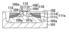
- FIG. 1A to FIG. 1Eare cross sections showing a fabrication method of a semiconductor device according to the first embodiment of the present invention.
- This semiconductor deviceincludes a P channel type MOS transistor on an N type well 103 a.
- an isolation region 102 composed of a buried insulating film or the likeis formed in a semiconductor substrate 101 of silicon or the like.
- the N type well 103 ais formed by photolithography and ion implantation.
- a gate insulating filmis formed on the upper surface of the semiconductor substrate 101 by thermal oxidation, and a non-doped polysilicon film is then formed on the gate insulating film.
- photolithography and ion implantationare carried out to introduce boron in the non-doped polysilicon film above the N type well 103 a .
- Photolithography and dry etchingare then carried out, thereby forming on the N type well 103 a a gate insulating film 104 and a P type gate electrode 105 a which have a given width.
- boron difluoride(BF 2 ) is introduced in regions of the N type well 103 a on both sides of the P type gate electrode 105 a , thereby forming P type extension regions 106 a .
- Phosphorusis introduced in the P type extension regions 106 a , thereby forming N type pocket regions 107 a below the P type extension regions 106 a.
- a TEOS film and a silicon nitride filmare formed on the silicon substrate 101 in order. Etch back is then carried out by anisotropic etch to form a side wall 110 composed of a TEOS film 108 a and a silicon nitride film 109 on side surfaces of the gate insulating film 104 and the P type gate electrode 105 a .
- the steps aboveare the same as those of the conventional fabrication method shown in FIG. 5A to FIG. 5C .
- photolithography and ion implantationare carried out to introduce indium in the N type well 103 a using a photoresist (not shown), the P type gate electrode 105 a and the side wall 110 as a mask, thereby forming first P type source/drain regions 111 c .
- Boronis then implanted to form second P type source/drain regions 111 d .
- the implantation conditions at this timeare, for example, an acceleration energy of 30 keV and a dose of 1 ⁇ 10 15 cm ⁇ 2 for indium and an acceleration energy of 1.5 keV and a dose of 4 ⁇ 10 15 cm ⁇ 2 for boron.
- the first P type source/drain regions 111 c and the second P type source/drain regions 111 dare together referred to as P type source/drain regions 111 a.
- the boron outside the indiumis diffused in the semiconductor substrate 101 by a subsequent heat treatment. As a result, the junction between the semiconductor substrate 101 and the P type source/drain regions 111 a is formed at a deeper portion and short-channel characteristics of the P channel type MOS transistor become deteriorated. To avoid this, boron is implanted such that the implantation depth of the boron is shallower than that of indium.
- the impurities introduced in the P type gate electrode 105 a and the N type well 103 aare activated by spike annealing.
- the process temperature at this timeis 1050° C., for example.
- the surface of the semiconductor substrate 101is cleaned with a hydrofluoric acid solution, thereby removing a natural oxide film on the surface of the substrate.
- a nickel metal film having a thickness of 9 nm, for example, and a titanium nitride (TiN) metal film having a thickness of 20 nmare formed on the semiconductor substrate 101 in order.
- the silicon substrate 101is subjected to a heat treatment in a nitrogen atmosphere under the conditions of, for example, 320° C.
- the nickel metal film and the titanium nitride metal film which have not reacted with siliconare removed with a solution in which sulfuric acid and hydrogen peroxide are mixed.
- the silicon substrate 101is again subjected to a heat treatment in a nitrogen atmosphere under the conditions of, for example, 550° C. for 30 seconds to form nickel silicide 112 on the P type gate electrode 105 a and the P type source/drain regions 111 a.
- FIG. 2Ais a cross sectional picture of a nickel silicide film formed on each of P type source/drain regions by a conventional fabrication method.
- FIG. 2Bis a cross sectional picture of a nickel silicide film formed on each of P type source/drain regions by a fabrication method of the present invention. It is apparent from comparison between these pictures that the thickness of the nickel silicide film formed by the fabrication method of the present embodiment is thinner than the thickness of the nickel silicide film formed by a conventional fabrication method.
- a silicon crystalis once made amorphous and then recrystallized by a subsequent heat treatment. Crystal defects remaining in the source/drain regions can be corrected by this process.
- FIG. 3shows normal probability distributions of a junction leakage current flowing from a source/drain region to a well in the respective P channel type MOS transistor arrays formed by a conventional fabrication method (line “a”) and a fabrication method of the present invention (line “b”). It is apparent from the drawing that the junction leakage current is reduced more in the P channel type MOS transistor array formed by the fabrication method of the present embodiment than the P channel type MOS transistor array formed by the conventional fabrication method.
- junction leakage currentis reduced because the reduction in thickness of the nickel silicide film results in increase in the distance between the bottom surface of the nickel silicide film and the junction interface. This is an effect of the fabrication method of the present embodiment.
- FIG. 4shows short-channel characteristics of the respective P channel type MOS transistors formed by a conventional fabrication method (line “a”) and a fabrication method of the present invention (line “b”). It is apparent from the drawing that the short-channel characteristics do not differ between the two fabrication methods and that shallow junction of the source/drain regions is also maintained by the fabrication method of the present invention. Thus, the fabrication method of the present embodiment is capable of suppressing abnormal growth of the silicide film and reducing leakage current, while keeping shallow junction depth of the source/drain regions.
- Implantation conditions of indiumare given in the above description. However, the above effect can also be obtained as long as an acceleration energy is in a range of 19 keV and 40 keV and a dose is in a range of 1 ⁇ 10 14 cm ⁇ 2 to 1 ⁇ 10 16 cm ⁇ 2 .
- the indiummay be replaced with gallium which also exhibits P type conductivity in silicon and whose atomic radius is greater than that of silicon as with indium.
- nickel silicideby using a nickel metal film to which at least one or more of platinum, aluminum, copper, erbium and palladium is added does not only provide the above effect, but also improve heat resistance of the nickel silicide.
- the gate length of the gate electrodeis not specified in the fabrication method of the present embodiment, the gate length is preferably 100 nm or less because problems of a silicide film become noticeable if the gate length exceeds the figure.
- the method of the present inventionis useful as a fabrication method of various semiconductor devices which include, for example, a P channel type MIS transistor.
Landscapes
- Electrodes Of Semiconductors (AREA)
- Insulated Gate Type Field-Effect Transistor (AREA)
Abstract
Description
Claims (8)
Priority Applications (1)
| Application Number | Priority Date | Filing Date | Title |
|---|---|---|---|
| US12/942,503US8247875B2 (en) | 2008-01-30 | 2010-11-09 | Fabrication method of semiconductor device |
Applications Claiming Priority (4)
| Application Number | Priority Date | Filing Date | Title |
|---|---|---|---|
| JP2008-018856 | 2008-01-30 | ||
| JP2008018856AJP2009182089A (en) | 2008-01-30 | 2008-01-30 | Manufacturing method of semiconductor device |
| US12/362,326US7851316B2 (en) | 2008-01-30 | 2009-01-29 | Fabrication method of semiconductor device |
| US12/942,503US8247875B2 (en) | 2008-01-30 | 2010-11-09 | Fabrication method of semiconductor device |
Related Parent Applications (1)
| Application Number | Title | Priority Date | Filing Date |
|---|---|---|---|
| US12/362,326DivisionUS7851316B2 (en) | 2008-01-30 | 2009-01-29 | Fabrication method of semiconductor device |
Publications (2)
| Publication Number | Publication Date |
|---|---|
| US20110049644A1 US20110049644A1 (en) | 2011-03-03 |
| US8247875B2true US8247875B2 (en) | 2012-08-21 |
Family
ID=40899656
Family Applications (2)
| Application Number | Title | Priority Date | Filing Date |
|---|---|---|---|
| US12/362,326ActiveUS7851316B2 (en) | 2008-01-30 | 2009-01-29 | Fabrication method of semiconductor device |
| US12/942,503Expired - Fee RelatedUS8247875B2 (en) | 2008-01-30 | 2010-11-09 | Fabrication method of semiconductor device |
Family Applications Before (1)
| Application Number | Title | Priority Date | Filing Date |
|---|---|---|---|
| US12/362,326ActiveUS7851316B2 (en) | 2008-01-30 | 2009-01-29 | Fabrication method of semiconductor device |
Country Status (2)
| Country | Link |
|---|---|
| US (2) | US7851316B2 (en) |
| JP (1) | JP2009182089A (en) |
Families Citing this family (1)
| Publication number | Priority date | Publication date | Assignee | Title |
|---|---|---|---|---|
| KR101068575B1 (en)* | 2009-07-03 | 2011-09-30 | 주식회사 하이닉스반도체 | Semiconductor device and manufacturing method thereof |
Citations (16)
| Publication number | Priority date | Publication date | Assignee | Title |
|---|---|---|---|---|
| JPH0333528A (en) | 1989-02-10 | 1991-02-13 | Lord Corp | Method of operating oscillation attenuator with semiactive damper means |
| US5675172A (en) | 1994-05-17 | 1997-10-07 | Hitachi, Ltd. | Metal-insulator-semiconductor device having reduced threshold voltage and high mobility for high speed/low-voltage operation |
| US5710055A (en) | 1994-12-01 | 1998-01-20 | Lucent Technologies Inc. | Method of making PMOSFETs having indium or gallium doped buried channels and n+ polysilicon gates and CMOS devices fabricated therefrom |
| JPH1116855A (en) | 1997-06-26 | 1999-01-22 | Nec Corp | Semiconductor device and its manufacture |
| US6087208A (en) | 1998-03-31 | 2000-07-11 | Advanced Micro Devices, Inc. | Method for increasing gate capacitance by using both high and low dielectric gate material |
| US6432802B1 (en) | 1999-09-17 | 2002-08-13 | Matsushita Electronics Corporation | Method for fabricating semiconductor device |
| US6483155B1 (en)* | 2001-06-29 | 2002-11-19 | Fujitsu Limtied | Semiconductor device having pocket and manufacture thereof |
| US6887758B2 (en) | 2002-10-09 | 2005-05-03 | Freescale Semiconductor, Inc. | Non-volatile memory device and method for forming |
| US6977417B2 (en) | 2002-06-24 | 2005-12-20 | Fujitsu Limited | Semiconductor device and method of fabricating the same |
| US20060071278A1 (en) | 2004-09-27 | 2006-04-06 | Fujitsu Limited | Semiconductor device and method for fabricating the same |
| US7098110B2 (en) | 2002-06-07 | 2006-08-29 | Fujitsu Limited | Semiconductor device and method of manufacturing thereof |
| US20060214198A1 (en) | 2005-03-23 | 2006-09-28 | Nec Electronics Corporation | Semiconductor device and manufacturing method thereof |
| US7141840B2 (en) | 2002-03-01 | 2006-11-28 | Renesas Technology Corp. | Semiconductor device and production method therefor |
| US7211516B2 (en) | 2005-04-01 | 2007-05-01 | Texas Instruments Incorporated | Nickel silicide including indium and a method of manufacture therefor |
| US7262105B2 (en) | 2003-11-21 | 2007-08-28 | Freescale Semiconductor, Inc. | Semiconductor device with silicided source/drains |
| US20110241127A1 (en)* | 2010-04-05 | 2011-10-06 | Taiwan Semiconductor Manufacturing Company, Ltd. | Well implant through dummy gate oxide in gate-last process |
Family Cites Families (8)
| Publication number | Priority date | Publication date | Assignee | Title |
|---|---|---|---|---|
| JP3545526B2 (en)* | 1996-01-19 | 2004-07-21 | 株式会社東芝 | Method for manufacturing semiconductor device |
| JP3746246B2 (en)* | 2002-04-16 | 2006-02-15 | 株式会社東芝 | Manufacturing method of semiconductor device |
| KR100870176B1 (en)* | 2003-06-27 | 2008-11-25 | 삼성전자주식회사 | Nickel alloy salicide process, method for manufacturing a semiconductor device using the same, nickel alloy silicide film formed thereby and a semiconductor device manufactured using the same |
| US20050253205A1 (en)* | 2004-05-17 | 2005-11-17 | Fujitsu Limited | Semiconductor device and method for fabricating the same |
| JP2006013284A (en)* | 2004-06-29 | 2006-01-12 | Toshiba Corp | Semiconductor device and manufacturing method thereof |
| US7705405B2 (en)* | 2004-07-06 | 2010-04-27 | International Business Machines Corporation | Methods for the formation of fully silicided metal gates |
| JP2007067225A (en)* | 2005-08-31 | 2007-03-15 | Toshiba Corp | Semiconductor device and manufacturing method thereof |
| JP2007324187A (en)* | 2006-05-30 | 2007-12-13 | Matsushita Electric Ind Co Ltd | Semiconductor device and manufacturing method thereof |
- 2008
- 2008-01-30JPJP2008018856Apatent/JP2009182089A/enactivePending
- 2009
- 2009-01-29USUS12/362,326patent/US7851316B2/enactiveActive
- 2010
- 2010-11-09USUS12/942,503patent/US8247875B2/ennot_activeExpired - Fee Related
Patent Citations (17)
| Publication number | Priority date | Publication date | Assignee | Title |
|---|---|---|---|---|
| JPH0333528A (en) | 1989-02-10 | 1991-02-13 | Lord Corp | Method of operating oscillation attenuator with semiactive damper means |
| US5675172A (en) | 1994-05-17 | 1997-10-07 | Hitachi, Ltd. | Metal-insulator-semiconductor device having reduced threshold voltage and high mobility for high speed/low-voltage operation |
| US5710055A (en) | 1994-12-01 | 1998-01-20 | Lucent Technologies Inc. | Method of making PMOSFETs having indium or gallium doped buried channels and n+ polysilicon gates and CMOS devices fabricated therefrom |
| JPH1116855A (en) | 1997-06-26 | 1999-01-22 | Nec Corp | Semiconductor device and its manufacture |
| JP3033528B2 (en) | 1997-06-26 | 2000-04-17 | 日本電気株式会社 | Semiconductor device and manufacturing method thereof |
| US6087208A (en) | 1998-03-31 | 2000-07-11 | Advanced Micro Devices, Inc. | Method for increasing gate capacitance by using both high and low dielectric gate material |
| US6432802B1 (en) | 1999-09-17 | 2002-08-13 | Matsushita Electronics Corporation | Method for fabricating semiconductor device |
| US6483155B1 (en)* | 2001-06-29 | 2002-11-19 | Fujitsu Limtied | Semiconductor device having pocket and manufacture thereof |
| US7141840B2 (en) | 2002-03-01 | 2006-11-28 | Renesas Technology Corp. | Semiconductor device and production method therefor |
| US7098110B2 (en) | 2002-06-07 | 2006-08-29 | Fujitsu Limited | Semiconductor device and method of manufacturing thereof |
| US6977417B2 (en) | 2002-06-24 | 2005-12-20 | Fujitsu Limited | Semiconductor device and method of fabricating the same |
| US6887758B2 (en) | 2002-10-09 | 2005-05-03 | Freescale Semiconductor, Inc. | Non-volatile memory device and method for forming |
| US7262105B2 (en) | 2003-11-21 | 2007-08-28 | Freescale Semiconductor, Inc. | Semiconductor device with silicided source/drains |
| US20060071278A1 (en) | 2004-09-27 | 2006-04-06 | Fujitsu Limited | Semiconductor device and method for fabricating the same |
| US20060214198A1 (en) | 2005-03-23 | 2006-09-28 | Nec Electronics Corporation | Semiconductor device and manufacturing method thereof |
| US7211516B2 (en) | 2005-04-01 | 2007-05-01 | Texas Instruments Incorporated | Nickel silicide including indium and a method of manufacture therefor |
| US20110241127A1 (en)* | 2010-04-05 | 2011-10-06 | Taiwan Semiconductor Manufacturing Company, Ltd. | Well implant through dummy gate oxide in gate-last process |
Non-Patent Citations (1)
| Title |
|---|
| The 63rd Annual Meeting of the Japanese Society of Microscopy, MG20-E-1430, with Partial English Translation. |
Also Published As
| Publication number | Publication date |
|---|---|
| JP2009182089A (en) | 2009-08-13 |
| US20090191682A1 (en) | 2009-07-30 |
| US20110049644A1 (en) | 2011-03-03 |
| US7851316B2 (en) | 2010-12-14 |
Similar Documents
| Publication | Publication Date | Title |
|---|---|---|
| US6475888B1 (en) | Method for forming ultra-shallow junctions using laser annealing | |
| US10043902B2 (en) | Semiconductor devices with shaped portions of elevated source/drain regions | |
| TWI382536B (en) | Low noise transistor and its preparation method | |
| US20130049199A1 (en) | Silicidation of device contacts using pre-amorphization implant of semiconductor substrate | |
| US7247919B1 (en) | Method and device to reduce gate-induced drain leakage (GIDL) current in thin gate oxides MOSFETs | |
| JP4299866B2 (en) | Manufacturing method of semiconductor device | |
| CN101140954B (en) | Semiconductor device | |
| US7365404B2 (en) | Semiconductor device having silicide reaction blocking region | |
| US8247875B2 (en) | Fabrication method of semiconductor device | |
| US7235450B2 (en) | Methods for fabricating semiconductor devices | |
| US7084458B1 (en) | Semiconductor device having triple LDD structure and lower gate resistance formed with a single implant process | |
| JP2004228351A (en) | Semiconductor device and manufacturing method thereof | |
| JP2020035789A (en) | Semiconductor device | |
| JP2003318176A (en) | Method of forming silicon oxide nitride film, semiconductor device, and method of manufacturing the same | |
| KR100190380B1 (en) | How to increase the cell ratio of drive transistors to access transistors | |
| US6313032B1 (en) | Method for manufacturing a salicide transistor, semiconductor storage, and semiconductor device | |
| JP5159708B2 (en) | Semiconductor device and manufacturing method thereof | |
| KR100596927B1 (en) | MOS transistor and its manufacturing method | |
| JPH11150118A (en) | Manufacture of semiconductor device | |
| KR100353466B1 (en) | A transistor and method for manufacturing the same | |
| KR100774790B1 (en) | Method of manufacturing a semiconductor device having a dummy spacer | |
| KR100289394B1 (en) | Method for producing a self aligned type epitaxial co silicide in semiconductor device | |
| KR100600253B1 (en) | Semiconductor device manufacturing method | |
| JP2005159336A (en) | Method for manufacturing semiconductor device | |
| JP2003530690A (en) | Method for manufacturing semiconductor device |
Legal Events
| Date | Code | Title | Description |
|---|---|---|---|
| ZAAA | Notice of allowance and fees due | Free format text:ORIGINAL CODE: NOA | |
| ZAAB | Notice of allowance mailed | Free format text:ORIGINAL CODE: MN/=. | |
| STCF | Information on status: patent grant | Free format text:PATENTED CASE | |
| FEPP | Fee payment procedure | Free format text:PAYOR NUMBER ASSIGNED (ORIGINAL EVENT CODE: ASPN); ENTITY STATUS OF PATENT OWNER: LARGE ENTITY | |
| AS | Assignment | Owner name:PANNOVA SEMIC, LLC, CALIFORNIA Free format text:ASSIGNMENT OF ASSIGNORS INTEREST;ASSIGNOR:PANASONIC CORPORATION;REEL/FRAME:036065/0273 Effective date:20141226 | |
| FPAY | Fee payment | Year of fee payment:4 | |
| FEPP | Fee payment procedure | Free format text:PAYER NUMBER DE-ASSIGNED (ORIGINAL EVENT CODE: RMPN); ENTITY STATUS OF PATENT OWNER: LARGE ENTITY Free format text:PAYOR NUMBER ASSIGNED (ORIGINAL EVENT CODE: ASPN); ENTITY STATUS OF PATENT OWNER: LARGE ENTITY | |
| MAFP | Maintenance fee payment | Free format text:PAYMENT OF MAINTENANCE FEE, 8TH YEAR, LARGE ENTITY (ORIGINAL EVENT CODE: M1552); ENTITY STATUS OF PATENT OWNER: LARGE ENTITY Year of fee payment:8 | |
| FEPP | Fee payment procedure | Free format text:MAINTENANCE FEE REMINDER MAILED (ORIGINAL EVENT CODE: REM.); ENTITY STATUS OF PATENT OWNER: LARGE ENTITY | |
| LAPS | Lapse for failure to pay maintenance fees | Free format text:PATENT EXPIRED FOR FAILURE TO PAY MAINTENANCE FEES (ORIGINAL EVENT CODE: EXP.); ENTITY STATUS OF PATENT OWNER: LARGE ENTITY | |
| STCH | Information on status: patent discontinuation | Free format text:PATENT EXPIRED DUE TO NONPAYMENT OF MAINTENANCE FEES UNDER 37 CFR 1.362 | |
| FP | Lapsed due to failure to pay maintenance fee | Effective date:20240821 |