US8247850B2 - Dual interlayer dielectric stressor integration with a sacrificial underlayer film stack - Google Patents
Dual interlayer dielectric stressor integration with a sacrificial underlayer film stackDownload PDFInfo
- Publication number
- US8247850B2 US8247850B2US11/650,252US65025207AUS8247850B2US 8247850 B2US8247850 B2US 8247850B2US 65025207 AUS65025207 AUS 65025207AUS 8247850 B2US8247850 B2US 8247850B2
- Authority
- US
- United States
- Prior art keywords
- gate structure
- layer
- underlayer
- region
- stressor
- Prior art date
- Legal status (The legal status is an assumption and is not a legal conclusion. Google has not performed a legal analysis and makes no representation as to the accuracy of the status listed.)
- Active, expires
Links
Images


Classifications
- H—ELECTRICITY
- H01—ELECTRIC ELEMENTS
- H01L—SEMICONDUCTOR DEVICES NOT COVERED BY CLASS H10
- H01L21/00—Processes or apparatus adapted for the manufacture or treatment of semiconductor or solid state devices or of parts thereof
- H01L21/70—Manufacture or treatment of devices consisting of a plurality of solid state components formed in or on a common substrate or of parts thereof; Manufacture of integrated circuit devices or of parts thereof
- H01L21/71—Manufacture of specific parts of devices defined in group H01L21/70
- H01L21/768—Applying interconnections to be used for carrying current between separate components within a device comprising conductors and dielectrics
- H01L21/76801—Applying interconnections to be used for carrying current between separate components within a device comprising conductors and dielectrics characterised by the formation and the after-treatment of the dielectrics, e.g. smoothing
- H01L21/76829—Applying interconnections to be used for carrying current between separate components within a device comprising conductors and dielectrics characterised by the formation and the after-treatment of the dielectrics, e.g. smoothing characterised by the formation of thin functional dielectric layers, e.g. dielectric etch-stop, barrier, capping or liner layers
- H—ELECTRICITY
- H10—SEMICONDUCTOR DEVICES; ELECTRIC SOLID-STATE DEVICES NOT OTHERWISE PROVIDED FOR
- H10D—INORGANIC ELECTRIC SEMICONDUCTOR DEVICES
- H10D30/00—Field-effect transistors [FET]
- H10D30/60—Insulated-gate field-effect transistors [IGFET]
- H10D30/791—Arrangements for exerting mechanical stress on the crystal lattice of the channel regions
- H10D30/792—Arrangements for exerting mechanical stress on the crystal lattice of the channel regions comprising applied insulating layers, e.g. stress liners
- H—ELECTRICITY
- H10—SEMICONDUCTOR DEVICES; ELECTRIC SOLID-STATE DEVICES NOT OTHERWISE PROVIDED FOR
- H10D—INORGANIC ELECTRIC SEMICONDUCTOR DEVICES
- H10D84/00—Integrated devices formed in or on semiconductor substrates that comprise only semiconducting layers, e.g. on Si wafers or on GaAs-on-Si wafers
- H10D84/01—Manufacture or treatment
- H10D84/0123—Integrating together multiple components covered by H10D12/00 or H10D30/00, e.g. integrating multiple IGBTs
- H10D84/0126—Integrating together multiple components covered by H10D12/00 or H10D30/00, e.g. integrating multiple IGBTs the components including insulated gates, e.g. IGFETs
- H10D84/0128—Manufacturing their channels
- H—ELECTRICITY
- H10—SEMICONDUCTOR DEVICES; ELECTRIC SOLID-STATE DEVICES NOT OTHERWISE PROVIDED FOR
- H10D—INORGANIC ELECTRIC SEMICONDUCTOR DEVICES
- H10D84/00—Integrated devices formed in or on semiconductor substrates that comprise only semiconducting layers, e.g. on Si wafers or on GaAs-on-Si wafers
- H10D84/01—Manufacture or treatment
- H10D84/0123—Integrating together multiple components covered by H10D12/00 or H10D30/00, e.g. integrating multiple IGBTs
- H10D84/0126—Integrating together multiple components covered by H10D12/00 or H10D30/00, e.g. integrating multiple IGBTs the components including insulated gates, e.g. IGFETs
- H10D84/013—Manufacturing their source or drain regions, e.g. silicided source or drain regions
- H10D84/0133—Manufacturing common source or drain regions between multiple IGFETs
- H—ELECTRICITY
- H10—SEMICONDUCTOR DEVICES; ELECTRIC SOLID-STATE DEVICES NOT OTHERWISE PROVIDED FOR
- H10D—INORGANIC ELECTRIC SEMICONDUCTOR DEVICES
- H10D84/00—Integrated devices formed in or on semiconductor substrates that comprise only semiconducting layers, e.g. on Si wafers or on GaAs-on-Si wafers
- H10D84/01—Manufacture or treatment
- H10D84/0123—Integrating together multiple components covered by H10D12/00 or H10D30/00, e.g. integrating multiple IGBTs
- H10D84/0126—Integrating together multiple components covered by H10D12/00 or H10D30/00, e.g. integrating multiple IGBTs the components including insulated gates, e.g. IGFETs
- H10D84/0165—Integrating together multiple components covered by H10D12/00 or H10D30/00, e.g. integrating multiple IGBTs the components including insulated gates, e.g. IGFETs the components including complementary IGFETs, e.g. CMOS devices
- H10D84/0167—Manufacturing their channels
- H—ELECTRICITY
- H10—SEMICONDUCTOR DEVICES; ELECTRIC SOLID-STATE DEVICES NOT OTHERWISE PROVIDED FOR
- H10D—INORGANIC ELECTRIC SEMICONDUCTOR DEVICES
- H10D84/00—Integrated devices formed in or on semiconductor substrates that comprise only semiconducting layers, e.g. on Si wafers or on GaAs-on-Si wafers
- H10D84/01—Manufacture or treatment
- H10D84/02—Manufacture or treatment characterised by using material-based technologies
- H10D84/03—Manufacture or treatment characterised by using material-based technologies using Group IV technology, e.g. silicon technology or silicon-carbide [SiC] technology
- H10D84/038—Manufacture or treatment characterised by using material-based technologies using Group IV technology, e.g. silicon technology or silicon-carbide [SiC] technology using silicon technology, e.g. SiGe
Definitions
- the present disclosurerelates generally to semiconductor devices, and more particularly to methods for making semiconductor devices having dual etch stop layer (ESL) stressor structures.
- ESLetch stop layer
- CMOS deviceshave been found to improve the performance characteristics of these devices.
- the presence of strain in the channel layercauses the individual silicon atoms within that layer to be forced farther apart or closer together in their lattice structure than would be the case in the unstrained material.
- the larger or smaller lattice spacingresults in a change in the electronic band structure of the device such that current carriers (i.e., electrons and holes) have higher mobilities within the channel layer, thereby resulting in higher currents in the transistor and faster circuit speeds.
- strained channel layersmay be achieved by imparting local mechanical stresses to the device. Electron mobility, and therefore NMOS performance, may be improved by imparting tensile stress along (i.e., parallel to) the direction of current flow or orthogonal to the direction of current flow. Hole mobility, and therefore PMOS performance, may be enhanced by imparting compressive stress parallel to the direction of current flow, and by imparting tensile stress perpendicular to the direction of current flow.
- ESLContact etch stop layer
- tensile stressmay be imparted to an NMOS channel by applying a tensile etch stop film
- compressive stressmay be imparted to a PMOS channel by applying a compressive etch stop film.
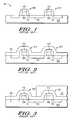
- FIG. 1illustrates a step in a prior art process for making a dual stressor structure
- FIG. 2illustrates a step in a prior art process for making a dual stressor structure
- FIG. 3illustrates a step in a prior art process for making a dual stressor structure
- FIG. 4illustrates a step in a prior art process for making a dual stressor structure
- FIG. 5illustrates a step in a prior art process for making a dual stressor structure
- FIG. 6illustrates a step in a prior art process for making a dual stressor structure
- FIG. 7illustrates a step in a prior art process for making a dual stressor structure
- FIG. 8illustrates a step in a prior art process for making a dual stressor structure
- FIG. 9illustrates a step in a prior art process for making a dual stressor structure
- FIG. 10illustrates a step in a process for making a dual stressor structure in accordance with the teachings herein;
- FIG. 11illustrates a step in a process for making a dual stressor structure in accordance with the teachings herein;
- FIG. 12illustrates a step in a process for making a dual stressor structure in accordance with the teachings herein;
- FIG. 13illustrates a step in a process for making a dual stressor structure in accordance with the teachings herein;
- FIG. 14illustrates a step in a process for making a dual stressor structure in accordance with the teachings herein;
- FIG. 15illustrates a step in a process for making a dual stressor structure in accordance with the teachings herein;
- FIG. 16illustrates a step in a process for making a dual stressor structure in accordance with the teachings herein;
- FIG. 17illustrates a step in a process for making a dual stressor structure in accordance with the teachings herein;
- FIG. 18illustrates a step in a process for making a dual stressor structure in accordance with the teachings herein;
- FIG. 19illustrates a step in a process for making a dual stressor structure in accordance with the teachings herein;
- FIG. 20illustrates a step in a process for making a dual stressor structure in accordance with the teachings herein;
- FIG. 21illustrates a step in a process for making a dual stressor structure in accordance with the teachings herein.
- a method for making a semiconductor devicefor (a) providing a substrate having first and second gate structures thereon; (b) forming an underlayer over the first and second gate structures; (c) removing the underlayer from the first gate structure; (d) forming a first stressor layer over the first and second gate structures; and (e) selectively removing the first stressor layer from the second gate structure through the use of a first etch which uses the underlayer as an etch stop layer.
- a method for making a semiconductor devicefor (a) providing a substrate having first and second gate structures thereon, wherein the first gate structure is disposed in an NMOS region of the device, and wherein the second gate structure is disposed in a PMOS region of the device; (b) forming an underlayer over the substrate; (c) forming a first layer of stress inducing material over the underlayer; (d) masking the device such that the first gate structure is exposed and the second gate structure is covered; and (e) removing the first layer of stress inducing material from the first gate structure with a first wet etch which is selective to the underlayer.
- a semiconductor devicehaving (a) a substrate having first and second gate structures thereon, wherein the first gate structure is disposed in an NMOS region of the device, and wherein the second gate structure is disposed in a PMOS region of the device; (b) an underlayer disposed over the substrate; and (c) a first layer of stress inducing material disposed over the underlayer.
- FIGS. 1-9The methodologies disclosed herein may be appreciated in the context of the prior art process depicted in FIGS. 1-9 .
- the process depicted thereinis a known process for making a MOSFET device with a dual etch stop layer (ESL) stressor integration.
- ESLetch stop layer
- tensile films and compressive filmsare selectively applied to the NMOS and PMOS regions, respectively, of a CMOS transistor.
- FIGS. 10-20the structures depicted in these figures (as well as in subsequent FIGS. 10-20 ) have been simplified for ease and clarity of illustration.
- the NMOS and PMOS regions in a semiconductor devicewill typically be isolated from each other by way of one or more trench isolation structures.
- a structure 101which comprises a substrate 103 upon which are defined first 105 and second 107 gate structures corresponding, respectively, to the PMOS and NMOS regions of a CMOS device.
- Each of the gate structures 105 , 107comprises a gate electrode 109 and adjacent spacer structures 111 .
- a layer of silicide 113is present on the gate electrodes 109 and the portions of the substrate 103 adjacent thereto.
- a tensile stressor layer 115is deposited over the structure.
- the tensile stressor layer 115is preferably deposited as a conformal layer.
- a first layer of photoresist 117is then deposited over the structure and is patterned such that the region of the structure containing the first gate structure 105 is exposed, and the region of the structure containing the second gate structure 107 is masked.
- the exposed portion of the tensile stressor layer 115is then removed from the device with a dry etch, as shown in FIG. 4 .
- the first layer of photoresist 117is then stripped as shown in FIG. 5 , after which a conformal compressive stressor layer 119 is deposited over the structure, as shown in FIG. 6 .
- a second layer of photoresist 121is deposited over the structure and is patterned such that the region of the structure containing the second gate structure 107 is exposed, and the region of the structure containing the first gate structure 105 is masked. As shown in FIG. 8 , the compressive stressor layer 119 is then removed from the exposed region with a suitable etchant. The second layer of photoresist 121 is then stripped to yield the structure shown in FIG. 9 .
- the structure depicted thereinhas a compressive stressor layer 119 disposed over the first gate structure 105 of the device, and a tensile stressor layer 115 disposed over the second gate structure 107 of the device.
- CMOS transistorsby selectively applying tensile films and compressive films, respectively, to only the NMOS and PMOS regions of these devices
- this processsuffers from some notable infirmities.
- this processrelies on dry etching to remove the portion of the tensile stressor layer 115 which extends over the first gate structure 105 (see FIG. 4 ) in the PMOS region of the device.
- dry etchingfrequently leaves behind some residue 116 (see FIG. 4 ) of the stressor film adjacent to the spacer.
- a (preferably isotropic) wet etchin conjunction with a sacrificial underlayer, such as a TiN film capped with an oxide hard mask film.
- the sacrificial underlayeracts as an etch stop for the wet and dry etch, thus allowing complete removal of the overlying stressor film from regions of the device in which its presence is not desired.
- the sacrificial underlayeralso protects the underlying features of the device from exposure to the etch and, in particular, protects the silicide regions of the device from gouging.
- the sacrificial underlayer film (or portions thereof)may be subsequently removed with a suitable wet or dry etch.
- FIGS. 10-21A first particular, non-limiting embodiment of the methodology disclosed herein is depicted in FIGS. 10-21 .
- the processbegins with a structure 201 which is similar to the structure depicted in FIG. 1 .
- This structure 201comprises a semiconductor substrate 203 upon which are defined first 205 and second 207 gate structures corresponding, respectively, to the PMOS and NMOS regions of a CMOS transistor.
- Each of the gate structures 205 , 207comprises a gate electrode 209 and adjacent spacer structures 211 .
- a layer of metal silicide 213is present on the gate electrodes 209 and on the portions of the substrate 203 adjacent thereto.
- the substrate 203has been depicted as a monolithic structure for simplicity of illustration, it will be appreciated that the substrate may comprise various layers or structures as are known to the art, including trench isolation structures and source/drain regions, and may include bulk or SOI wafers.
- an underlayer 231is deposited over the structure.
- the underlayer 231 in this particular embodimentcomprises a sub-layer of TiN 235 over which has been deposited an oxide hard mask sub-layer 233 .
- a first layer of photoresist 217is then deposited over the structure, and is patterned such that the region of the structure containing the first gate structure 205 is exposed, while the region of the structure containing the second gate structure 207 is masked.
- the oxide hard mask sub-layer 233is then removed from the exposed portion of the device with a suitable etch, as shown in FIG. 13 .
- this etchis an aqueous HF etch.
- the first layer of photoresist 217is removed, preferably through oxygen ashing.
- the exposed portion of the TiN sub-layer 235is also removed with a suitably etchant, preferably Pir/SC1 (Pir, or “Piranha”, also known as SPM (Sulfuric Peroxide Mixture), is a mixture of H 2 SO 4 and H 2 O 2 ; SC1, or “Standard Clean 1”, is a mixture of NH 4 OH and H 2 O 2 ).
- a suitably etchantpreferably Pir/SC1 (Pir, or “Piranha”, also known as SPM (Sulfuric Peroxide Mixture), is a mixture of H 2 SO 4 and H 2 O 2 ; SC1, or “Standard Clean 1”, is a mixture of NH 4 OH and H 2 O 2 ).
- a compressive stressor layer 216is deposited over the structure.
- the compressive stressor layer 216is preferably deposited as a conformal layer.
- a second layer of photoresist 221is then deposited over the structure as shown in FIG. 16 .
- the second layer of photoresist 221is patterned such that the region of the structure containing the second gate structure 207 is exposed, while the region of the structure containing the first gate structure 205 is masked.
- the exposed portion of the compressive stressor layer 216is then removed with a suitable etch.
- a suitable dry etchis used to remove the bulk of the compressive stressor layer 216 .
- the underlayer 231(and in particular, the oxide hard mask sub-layer 233 thereof) is used as an etch stop during the dry etch.
- the dry etch used herepreferably has high selectivity to the oxide hard mask sub-layer 233 .
- the residual portion of the compressive stressor layer 216(which will typically be present in areas adjacent to the gate structure 207 ) is removed with an isotropic aqueous HF etch.
- the isotropic aqueous HF etchpreferably also removes the oxide hard mask sub-layer 233 .
- the second layer of photoresist 221is then stripped with oxygen ashing, and the remaining portion of the TiN sub-layer 235 is then removed with Pir/SC1.
- a suitable etchmay be used to remove the entire exposed portion of the underlayer 231 (including both the oxide hard mask sub-layer 233 and the TiN sub-layer 235 ) prior to removal of the second layer of photoresist 221 .
- the etch used for this purposeis preferably selective to the metal silicide 213 and the spacer structures 211 .
- this etchmay comprise multiple etches, and each of the multiple etches may have a unique chemistry.
- a tensile stressor layer 219is then deposited over the structure.
- the tensile stressor layer 219is preferably deposited as a conformal layer.
- a third layer of photoresist 223is then deposited over the structure and is patterned such that the region of the structure containing the second gate structure 207 is masked, and the region of the structure containing the first gate structure 205 is exposed.
- the tensile stressor layer 219is then removed from the exposed region with a suitable etch.
- a suitable dry etchis used to remove the bulk of the tensile stressor layer 219 , and the residual portion of that layer (which will typically be present in areas adjacent to the gate structure 205 ) is removed with an isotropic aqueous HF etch.
- the compressive stressor layer 216is used as an etch stop in this process.
- the third layer of photoresist 223is then stripped, thus yielding the structure shown in FIG. 21 .
- the tensile layercould be deposited first. This could be achieved, for example, by modifying the procedure depicted in FIGS. 10-21 such that layer 216 is the tensile stressor layer and layer 219 is the compressive stressor layer, and such that the first 205 and second 207 gate structures correspond, respectively, to the NMOS and PMOS regions of the CMOS transistor. In such embodiments, suitable changes may be made to the etch chemistries.
- FIGS. 10-21has a number of advantages over the prior art process depicted in FIGS. 1-9 .
- the wet etch used in the prior art process of FIGS. 1-9can result in gouging of the metal silicide layer 213 , and consequent degradation of the electrical properties of the device.
- a dry etch followed by a wet etchis utilized to ensure complete removal of the unneeded portions of compressive stressor layer 216 (see FIG. 16 ), and the metal silicide layer is protected from gouging during this etching through the presence of the hard mask sub-layer 233 and the underlying TiN sub-layer 235 .
- the hard mask sub-layer 233 , and the underlying TiN sub-layer 235may be subsequently removed with an etch which has a high selectivity to the metal silicide 213 , which again prevents gouging of the metal silicide 213 .
- a wet or dry etchmay also be utilized to remove the unneeded portions of tensile stressor layer 219 (see FIG. 20 ). During this etch, which is preferably selective to the material of the compressive stressor layer 216 , the compressive stressor layer 216 prevents gouging of the metal silicide 213 .
- a very thin oxide filmmay be deposited after the deposition of the compressive stressor film 216 .
- This thin oxide filmmay act as an etch stop layer in the event of dry etch removal of the tensile stressor layer 219 from the PMOS regions of the device.
- the inclusion of this thin oxide filmmay also involve a prior additional breakthrough step in the etching of the compressive stressor layer 216 from the NMOS regions of the device.
- the materials used in the stressor layers in the methods and devices described hereinmay comprise refractory insulating materials, or materials with appropriate etch selectivity and appropriate physical properties.
- Such filmsmay comprise, for example, silicon nitride (e.g., Si 3 N 4 or Si x N y ) and/or silicon oxynitride (e.g., Si x ON y ).
- These materialsmay be grown or blanket deposited through suitable processes, such as chemical vapor deposition (CVD), plasma enhanced chemical vapor deposition (PECVD) or physical vapor deposition (PVD).
- CVDchemical vapor deposition
- PECVDplasma enhanced chemical vapor deposition
- PVDphysical vapor deposition
- the thicknesses of the individual layers utilized in the structures and methodologies described hereinmay also vary.
- the stressor layershave a thickness within the range of about 400 ⁇ to about 1200 ⁇ , preferably within the range of about 600 ⁇ to about 1000 ⁇ , more preferably within the range of about 700 ⁇ to about 900 ⁇ , and most preferably within the range of about 750 ⁇ to about 850 ⁇ .
- the individual layers of the sacrificial underlayerwill typically have thicknesses that are about a tenth of the foregoing thicknesses recited for the stressor layers.
- the physical properties of the stressor films described herein, including the type and magnitude of the stress that these films apply,may be selected through appropriate manipulation of the process parameters used to form the film.
- process parametersinclude, for example, deposition pressure, plasma power, process chemistry, and the spacing between the wafer and the electrode.
- a tensile film exhibiting a tensile stress of approximately greater than 1000 MPamay be achieved using the following CVD parameters: a temperature of approximately 350-500° C., a pressure of approximately 1-10 Torr, a spacing between the wafer and the electrode of 1.0-1.3 cm, a combination of process gases such as silane and ammonia and inert gases such as nitrogen, helium, and argon, and a total RF power density in a range of approximately 0.05-0.32 watts per square centimeter (W/cm 2 ).
- a compressive film exhibiting a compressive stress whose magnitude is approximately greater than ⁇ 2000 MPamay be achieved with the following CVD parameters: a temperature of approximately 350-500° C., a pressure of approximately 1-10 Torr, a spacing between the wafer and the electrode of 0.05-1.1 cm, a combination of process gases such as silane and ammonia and inert gases such as nitrogen, helium, and argon, and a total RF power density in a range of approximately 0.05-0.8 W/cm 2 .
- the sacrificial underlayermay comprise an oxide film, below which a high k dielectric material, such as HfO 2 , is used instead of a TiN film.
- a suitable etch chemistrysuch as, for example, hot HCl may then be used to strip the HfO 2 .
- HfO 2is suitable as an etch stop for removal of the overlying oxide film in dilute HF.
- any two materials which have sufficient etch selectivities with respect to different etch chemistriesmay be used as sacrificial underlayers in the structures and methodologies described herein. It will also be appreciated that the sacrificial underlayers described herein may, in some embodiments, have more than two layers, and may have more than two distinct materials.
- Various wet and dry etchesmay be used in the processes described herein to remove the remaining portion of the tensile stressor layer 219 from the PMOS region of the device (these etches may also be used in the processes described herein to remove the remaining portion of the tensile stressor layer 219 from the PMOS region of the device in embodiments in which the compressive stressor film is deposited first).
- Dry etching of the ESL filmscan be accomplished by using standard etch techniques using halogen containing gases, either alone or combined with other gases, which could include carrier gases. The choice of gases is dependent on the type of selectivities required.
- Possible etchant gasesmay include, but are not limited to, CF 4 , CHF 3 , CH 3 F, SF 6 , NF 3 , CH 2 F 2 , C 4 F 8 , C 4 F 6 , CO, N 2 , O 2 , He, and Ar.
- Suitable wet etchantsinclude, but are not limited to, dilute, aqueous solutions of HF, with HF: H 2 0 concentrations of approximately 1:50 to 1:1000.
Landscapes
- Engineering & Computer Science (AREA)
- Physics & Mathematics (AREA)
- Condensed Matter Physics & Semiconductors (AREA)
- General Physics & Mathematics (AREA)
- Manufacturing & Machinery (AREA)
- Computer Hardware Design (AREA)
- Microelectronics & Electronic Packaging (AREA)
- Power Engineering (AREA)
- Metal-Oxide And Bipolar Metal-Oxide Semiconductor Integrated Circuits (AREA)
- Insulated Gate Type Field-Effect Transistor (AREA)
Abstract
Description
Claims (20)
Priority Applications (1)
| Application Number | Priority Date | Filing Date | Title |
|---|---|---|---|
| US11/650,252US8247850B2 (en) | 2007-01-04 | 2007-01-04 | Dual interlayer dielectric stressor integration with a sacrificial underlayer film stack |
Applications Claiming Priority (1)
| Application Number | Priority Date | Filing Date | Title |
|---|---|---|---|
| US11/650,252US8247850B2 (en) | 2007-01-04 | 2007-01-04 | Dual interlayer dielectric stressor integration with a sacrificial underlayer film stack |
Publications (2)
| Publication Number | Publication Date |
|---|---|
| US20080164531A1 US20080164531A1 (en) | 2008-07-10 |
| US8247850B2true US8247850B2 (en) | 2012-08-21 |
Family
ID=39593522
Family Applications (1)
| Application Number | Title | Priority Date | Filing Date |
|---|---|---|---|
| US11/650,252Active2028-09-27US8247850B2 (en) | 2007-01-04 | 2007-01-04 | Dual interlayer dielectric stressor integration with a sacrificial underlayer film stack |
Country Status (1)
| Country | Link |
|---|---|
| US (1) | US8247850B2 (en) |
Cited By (1)
| Publication number | Priority date | Publication date | Assignee | Title |
|---|---|---|---|---|
| US20120104505A1 (en)* | 2010-10-28 | 2012-05-03 | International Business Machines Corporation | Structure and method for using high-k material as an etch stop layer in dual stress layer process |
Families Citing this family (8)
| Publication number | Priority date | Publication date | Assignee | Title |
|---|---|---|---|---|
| US7867893B2 (en)* | 2007-06-28 | 2011-01-11 | International Business Machines Corporation | Method of forming an SOI substrate contact |
| US7960223B2 (en)* | 2008-06-16 | 2011-06-14 | International Business Machines Corporation | Structure and method to integrate dual silicide with dual stress liner to improve CMOS performance |
| US7642147B1 (en)* | 2008-10-01 | 2010-01-05 | International Business Machines Corporation | Methods for removing sidewall spacers |
| CN102254914B (en)* | 2010-05-20 | 2013-03-13 | 中国科学院微电子研究所 | Semiconductor structure and forming method thereof |
| DE102010038744B4 (en) | 2010-07-30 | 2012-08-30 | GLOBALFOUNDRIES Dresden Module One Ltd. Liability Company & Co. KG | Increasing the robustness in a double stress layering process in a semiconductor device by applying wet chemistry |
| US9129796B2 (en)* | 2010-08-19 | 2015-09-08 | Texas Instruments Incorporated | Pre-metal deposition clean process |
| US10050035B2 (en) | 2014-01-17 | 2018-08-14 | Taiwan Semiconductor Manufacturing Company, Ltd. | Method of making protective layer over polysilicon structure |
| TWI741007B (en)* | 2017-08-16 | 2021-10-01 | 聯華電子股份有限公司 | Method of manufacturing interconnect structure |
Citations (13)
| Publication number | Priority date | Publication date | Assignee | Title |
|---|---|---|---|---|
| US20030181005A1 (en)* | 2002-03-19 | 2003-09-25 | Kiyota Hachimine | Semiconductor device and a method of manufacturing the same |
| WO2004049406A1 (en) | 2002-11-25 | 2004-06-10 | International Business Machines Corporation | Strained finfet cmos device structures |
| US20050093030A1 (en) | 2003-10-30 | 2005-05-05 | Doris Bruce B. | Structure and method to enhance both nFET and pFET performance using different kinds of stressed layers |
| US20050158970A1 (en)* | 2004-01-16 | 2005-07-21 | Robert Chau | Tri-gate transistors and methods to fabricate same |
| US20050263825A1 (en)* | 2004-05-28 | 2005-12-01 | Kai Frohberg | Technique for creating different mechanical stress in different channel regions by forming an etch stop layer having differently modified intrinsic stress |
| US20060091471A1 (en) | 2004-10-29 | 2006-05-04 | Kai Frohberg | Technique for creating different mechanical strain in different channel regions by forming an etch stop layer stack having differently modified intrinsic stress |
| US20060228848A1 (en)* | 2005-03-31 | 2006-10-12 | International Business Machines Corporation | Dual-hybrid liner formation without exposing silicide layer to photoresist stripping chemicals |
| US20070004199A1 (en)* | 1998-09-03 | 2007-01-04 | Ireland Philip J | Method of making a contact structure |
| US20070111452A1 (en)* | 2005-11-16 | 2007-05-17 | Pei-Yu Chou | fabricating method of cmos and mos device |
| US7262472B2 (en)* | 2004-06-08 | 2007-08-28 | Fujitsu Limited | Semiconductor device having stress and its manufacture method |
| US20070249113A1 (en)* | 2006-04-21 | 2007-10-25 | Freescale Semiconductor, Inc. | Stressor integration and method thereof |
| US20080073724A1 (en)* | 2006-09-22 | 2008-03-27 | Taiwan Semiconductor Manufacturing Co., Ltd. | Double layer etch stop layer structure for advanced semiconductor processing technology |
| US7432147B2 (en)* | 2004-12-28 | 2008-10-07 | Kabushiki Kaisha Toshiba | Method of manufacturing semiconductor device |
- 2007
- 2007-01-04USUS11/650,252patent/US8247850B2/enactiveActive
Patent Citations (13)
| Publication number | Priority date | Publication date | Assignee | Title |
|---|---|---|---|---|
| US20070004199A1 (en)* | 1998-09-03 | 2007-01-04 | Ireland Philip J | Method of making a contact structure |
| US20030181005A1 (en)* | 2002-03-19 | 2003-09-25 | Kiyota Hachimine | Semiconductor device and a method of manufacturing the same |
| WO2004049406A1 (en) | 2002-11-25 | 2004-06-10 | International Business Machines Corporation | Strained finfet cmos device structures |
| US20050093030A1 (en) | 2003-10-30 | 2005-05-05 | Doris Bruce B. | Structure and method to enhance both nFET and pFET performance using different kinds of stressed layers |
| US20050158970A1 (en)* | 2004-01-16 | 2005-07-21 | Robert Chau | Tri-gate transistors and methods to fabricate same |
| US20050263825A1 (en)* | 2004-05-28 | 2005-12-01 | Kai Frohberg | Technique for creating different mechanical stress in different channel regions by forming an etch stop layer having differently modified intrinsic stress |
| US7262472B2 (en)* | 2004-06-08 | 2007-08-28 | Fujitsu Limited | Semiconductor device having stress and its manufacture method |
| US20060091471A1 (en) | 2004-10-29 | 2006-05-04 | Kai Frohberg | Technique for creating different mechanical strain in different channel regions by forming an etch stop layer stack having differently modified intrinsic stress |
| US7432147B2 (en)* | 2004-12-28 | 2008-10-07 | Kabushiki Kaisha Toshiba | Method of manufacturing semiconductor device |
| US20060228848A1 (en)* | 2005-03-31 | 2006-10-12 | International Business Machines Corporation | Dual-hybrid liner formation without exposing silicide layer to photoresist stripping chemicals |
| US20070111452A1 (en)* | 2005-11-16 | 2007-05-17 | Pei-Yu Chou | fabricating method of cmos and mos device |
| US20070249113A1 (en)* | 2006-04-21 | 2007-10-25 | Freescale Semiconductor, Inc. | Stressor integration and method thereof |
| US20080073724A1 (en)* | 2006-09-22 | 2008-03-27 | Taiwan Semiconductor Manufacturing Co., Ltd. | Double layer etch stop layer structure for advanced semiconductor processing technology |
Non-Patent Citations (3)
| Title |
|---|
| H.S. Yang et al., "Dual Stress Liner for High Performance sub-45nm Gate Length SOI CMOS Manufacturing"; EIDM 2004 Late News; 2004 IEEE, 3 pages. |
| Pidin, S. et al.: "A Novel Strain Enhanced CMOS Architecture Using Selectively Deposited High Tensile and High Compressive Silicon Nitride Films"; IEEE 2004; 4 pages. |
| Wolf, S. Silicon Processing for the VLSI Era, 1986 Lattice Press vol. 1.* |
Cited By (3)
| Publication number | Priority date | Publication date | Assignee | Title |
|---|---|---|---|---|
| US20120104505A1 (en)* | 2010-10-28 | 2012-05-03 | International Business Machines Corporation | Structure and method for using high-k material as an etch stop layer in dual stress layer process |
| US8673757B2 (en)* | 2010-10-28 | 2014-03-18 | International Business Machines Corporation | Structure and method for using high-k material as an etch stop layer in dual stress layer process |
| US8946721B2 (en) | 2010-10-28 | 2015-02-03 | International Business Machines Corporation | Structure and method for using high-K material as an etch stop layer in dual stress layer process |
Also Published As
| Publication number | Publication date |
|---|---|
| US20080164531A1 (en) | 2008-07-10 |
Similar Documents
| Publication | Publication Date | Title |
|---|---|---|
| US7528029B2 (en) | Stressor integration and method thereof | |
| US8247850B2 (en) | Dual interlayer dielectric stressor integration with a sacrificial underlayer film stack | |
| JP5582582B2 (en) | Dual high-K oxide with SiGe channel | |
| CN100378901C (en) | Strained Fin Field Effect Transistor Complementary Metal Oxide Semiconductor Device Structure | |
| JP4906868B2 (en) | Structure and method for increasing strain enhancement by spacerless FET and dual liner method | |
| US7388259B2 (en) | Strained finFET CMOS device structures | |
| TWI411109B (en) | Semiconductor device and method of manufacturing the same | |
| US8415212B2 (en) | Method of enhancing photoresist adhesion to rare earth oxides | |
| JP4767946B2 (en) | Complementary metal oxide semiconductor integrated circuit with NMOS and PMOS transistors using different gate dielectrics | |
| CN1855431B (en) | Semiconductor manufacturing method | |
| JP4598639B2 (en) | Manufacturing method of semiconductor device | |
| US20070269970A1 (en) | Structure and method for forming cmos devices with intrinsically stressed silicide using silicon nitride cap | |
| CN1591838A (en) | Hybrid planar and FinFET CMOS devices | |
| JP2007134718A (en) | 2-stress memory technology in semiconductor devices | |
| US20140110793A1 (en) | Cmos transistor and fabrication method | |
| US20120018813A1 (en) | BARRIER COAT FOR ELIMINATION OF RESIST RESIDUES ON HIGH k/METAL GATE STACKS | |
| KR101197464B1 (en) | Method of manufacturing a semiconductor device | |
| US7091071B2 (en) | Semiconductor fabrication process including recessed source/drain regions in an SOI wafer | |
| JP4854245B2 (en) | Manufacturing method of semiconductor device | |
| TWI801628B (en) | Methods to protect nitride layers during formation of silicon germanium nano-wires in microelectronic workpieces | |
| US20080280429A1 (en) | Method to control uniformity/composition of metal electrodes, silicides on topography and devices using this method | |
| US20110278672A1 (en) | Methodology for fabricating isotropically recessed drain regions of cmos transistors | |
| US7579228B2 (en) | Disposable organic spacers | |
| JP2007036116A (en) | Semiconductor device manufacturing method | |
| US7402476B2 (en) | Method for forming an electronic device |
Legal Events
| Date | Code | Title | Description |
|---|---|---|---|
| AS | Assignment | Owner name:FREESCALE SEMICONDUCTOR, INC., TEXAS Free format text:ASSIGNMENT OF ASSIGNORS INTEREST;ASSIGNORS:JAWARANI, DHARMESH;NOBLE, ROSS E.;WANG, DAVID C.;REEL/FRAME:018776/0602 Effective date:20061208 | |
| AS | Assignment | Owner name:CITIBANK, N.A., NEW YORK Free format text:SECURITY AGREEMENT;ASSIGNOR:FREESCALE SEMICONDUCTOR, INC.;REEL/FRAME:019847/0804 Effective date:20070620 Owner name:CITIBANK, N.A.,NEW YORK Free format text:SECURITY AGREEMENT;ASSIGNOR:FREESCALE SEMICONDUCTOR, INC.;REEL/FRAME:019847/0804 Effective date:20070620 | |
| AS | Assignment | Owner name:CITIBANK, N.A.,NEW YORK Free format text:SECURITY AGREEMENT;ASSIGNOR:FREESCALE SEMICONDUCTOR, INC.;REEL/FRAME:024085/0001 Effective date:20100219 Owner name:CITIBANK, N.A., NEW YORK Free format text:SECURITY AGREEMENT;ASSIGNOR:FREESCALE SEMICONDUCTOR, INC.;REEL/FRAME:024085/0001 Effective date:20100219 | |
| AS | Assignment | Owner name:CITIBANK, N.A., AS COLLATERAL AGENT,NEW YORK Free format text:SECURITY AGREEMENT;ASSIGNOR:FREESCALE SEMICONDUCTOR, INC.;REEL/FRAME:024397/0001 Effective date:20100413 Owner name:CITIBANK, N.A., AS COLLATERAL AGENT, NEW YORK Free format text:SECURITY AGREEMENT;ASSIGNOR:FREESCALE SEMICONDUCTOR, INC.;REEL/FRAME:024397/0001 Effective date:20100413 | |
| FEPP | Fee payment procedure | Free format text:PAYOR NUMBER ASSIGNED (ORIGINAL EVENT CODE: ASPN); ENTITY STATUS OF PATENT OWNER: LARGE ENTITY | |
| STCF | Information on status: patent grant | Free format text:PATENTED CASE | |
| AS | Assignment | Owner name:CITIBANK, N.A., AS NOTES COLLATERAL AGENT, NEW YORK Free format text:SECURITY AGREEMENT;ASSIGNOR:FREESCALE SEMICONDUCTOR, INC.;REEL/FRAME:030633/0424 Effective date:20130521 Owner name:CITIBANK, N.A., AS NOTES COLLATERAL AGENT, NEW YOR Free format text:SECURITY AGREEMENT;ASSIGNOR:FREESCALE SEMICONDUCTOR, INC.;REEL/FRAME:030633/0424 Effective date:20130521 | |
| AS | Assignment | Owner name:CITIBANK, N.A., AS NOTES COLLATERAL AGENT, NEW YORK Free format text:SECURITY AGREEMENT;ASSIGNOR:FREESCALE SEMICONDUCTOR, INC.;REEL/FRAME:031591/0266 Effective date:20131101 Owner name:CITIBANK, N.A., AS NOTES COLLATERAL AGENT, NEW YOR Free format text:SECURITY AGREEMENT;ASSIGNOR:FREESCALE SEMICONDUCTOR, INC.;REEL/FRAME:031591/0266 Effective date:20131101 | |
| AS | Assignment | Owner name:FREESCALE SEMICONDUCTOR, INC., TEXAS Free format text:PATENT RELEASE;ASSIGNOR:CITIBANK, N.A., AS COLLATERAL AGENT;REEL/FRAME:037354/0640 Effective date:20151207 Owner name:FREESCALE SEMICONDUCTOR, INC., TEXAS Free format text:PATENT RELEASE;ASSIGNOR:CITIBANK, N.A., AS COLLATERAL AGENT;REEL/FRAME:037356/0143 Effective date:20151207 Owner name:FREESCALE SEMICONDUCTOR, INC., TEXAS Free format text:PATENT RELEASE;ASSIGNOR:CITIBANK, N.A., AS COLLATERAL AGENT;REEL/FRAME:037356/0553 Effective date:20151207 | |
| AS | Assignment | Owner name:MORGAN STANLEY SENIOR FUNDING, INC., MARYLAND Free format text:ASSIGNMENT AND ASSUMPTION OF SECURITY INTEREST IN PATENTS;ASSIGNOR:CITIBANK, N.A.;REEL/FRAME:037486/0517 Effective date:20151207 | |
| AS | Assignment | Owner name:MORGAN STANLEY SENIOR FUNDING, INC., MARYLAND Free format text:ASSIGNMENT AND ASSUMPTION OF SECURITY INTEREST IN PATENTS;ASSIGNOR:CITIBANK, N.A.;REEL/FRAME:037518/0292 Effective date:20151207 | |
| FPAY | Fee payment | Year of fee payment:4 | |
| AS | Assignment | Owner name:MORGAN STANLEY SENIOR FUNDING, INC., MARYLAND Free format text:SECURITY AGREEMENT SUPPLEMENT;ASSIGNOR:NXP B.V.;REEL/FRAME:038017/0058 Effective date:20160218 | |
| AS | Assignment | Owner name:MORGAN STANLEY SENIOR FUNDING, INC., MARYLAND Free format text:SUPPLEMENT TO THE SECURITY AGREEMENT;ASSIGNOR:FREESCALE SEMICONDUCTOR, INC.;REEL/FRAME:039138/0001 Effective date:20160525 | |
| AS | Assignment | Owner name:MORGAN STANLEY SENIOR FUNDING, INC., MARYLAND Free format text:CORRECTIVE ASSIGNMENT TO CORRECT THE REMOVE APPLICATION 12092129 PREVIOUSLY RECORDED ON REEL 038017 FRAME 0058. ASSIGNOR(S) HEREBY CONFIRMS THE SECURITY AGREEMENT SUPPLEMENT;ASSIGNOR:NXP B.V.;REEL/FRAME:039361/0212 Effective date:20160218 | |
| AS | Assignment | Owner name:NXP, B.V., F/K/A FREESCALE SEMICONDUCTOR, INC., NETHERLANDS Free format text:RELEASE BY SECURED PARTY;ASSIGNOR:MORGAN STANLEY SENIOR FUNDING, INC.;REEL/FRAME:040925/0001 Effective date:20160912 Owner name:NXP, B.V., F/K/A FREESCALE SEMICONDUCTOR, INC., NE Free format text:RELEASE BY SECURED PARTY;ASSIGNOR:MORGAN STANLEY SENIOR FUNDING, INC.;REEL/FRAME:040925/0001 Effective date:20160912 | |
| AS | Assignment | Owner name:NXP B.V., NETHERLANDS Free format text:RELEASE BY SECURED PARTY;ASSIGNOR:MORGAN STANLEY SENIOR FUNDING, INC.;REEL/FRAME:040928/0001 Effective date:20160622 | |
| AS | Assignment | Owner name:NXP USA, INC., TEXAS Free format text:CHANGE OF NAME;ASSIGNOR:FREESCALE SEMICONDUCTOR, INC.;REEL/FRAME:040632/0001 Effective date:20161107 | |
| AS | Assignment | Owner name:MORGAN STANLEY SENIOR FUNDING, INC., MARYLAND Free format text:CORRECTIVE ASSIGNMENT TO CORRECT THE REMOVE PATENTS 8108266 AND 8062324 AND REPLACE THEM WITH 6108266 AND 8060324 PREVIOUSLY RECORDED ON REEL 037518 FRAME 0292. ASSIGNOR(S) HEREBY CONFIRMS THE ASSIGNMENT AND ASSUMPTION OF SECURITY INTEREST IN PATENTS;ASSIGNOR:CITIBANK, N.A.;REEL/FRAME:041703/0536 Effective date:20151207 | |
| AS | Assignment | Owner name:MORGAN STANLEY SENIOR FUNDING, INC., MARYLAND Free format text:CORRECTIVE ASSIGNMENT TO CORRECT THE REMOVE APPLICATION 12681366 PREVIOUSLY RECORDED ON REEL 039361 FRAME 0212. ASSIGNOR(S) HEREBY CONFIRMS THE SECURITY AGREEMENT SUPPLEMENT;ASSIGNOR:NXP B.V.;REEL/FRAME:042762/0145 Effective date:20160218 Owner name:MORGAN STANLEY SENIOR FUNDING, INC., MARYLAND Free format text:CORRECTIVE ASSIGNMENT TO CORRECT THE REMOVE APPLICATION 12681366 PREVIOUSLY RECORDED ON REEL 038017 FRAME 0058. ASSIGNOR(S) HEREBY CONFIRMS THE SECURITY AGREEMENT SUPPLEMENT;ASSIGNOR:NXP B.V.;REEL/FRAME:042985/0001 Effective date:20160218 | |
| AS | Assignment | Owner name:NXP USA, INC., TEXAS Free format text:CORRECTIVE ASSIGNMENT TO CORRECT THE NATURE OF CONVEYANCE PREVIOUSLY RECORDED AT REEL: 040632 FRAME: 0001. ASSIGNOR(S) HEREBY CONFIRMS THE MERGER AND CHANGE OF NAME;ASSIGNOR:FREESCALE SEMICONDUCTOR INC.;REEL/FRAME:044209/0047 Effective date:20161107 | |
| AS | Assignment | Owner name:SHENZHEN XINGUODU TECHNOLOGY CO., LTD., CHINA Free format text:CORRECTIVE ASSIGNMENT TO CORRECT THE TO CORRECT THE APPLICATION NO. FROM 13,883,290 TO 13,833,290 PREVIOUSLY RECORDED ON REEL 041703 FRAME 0536. ASSIGNOR(S) HEREBY CONFIRMS THE THE ASSIGNMENT AND ASSUMPTION OF SECURITYINTEREST IN PATENTS.;ASSIGNOR:MORGAN STANLEY SENIOR FUNDING, INC.;REEL/FRAME:048734/0001 Effective date:20190217 | |
| AS | Assignment | Owner name:NXP B.V., NETHERLANDS Free format text:RELEASE BY SECURED PARTY;ASSIGNOR:MORGAN STANLEY SENIOR FUNDING, INC.;REEL/FRAME:050744/0097 Effective date:20190903 Owner name:NXP B.V., NETHERLANDS Free format text:RELEASE BY SECURED PARTY;ASSIGNOR:MORGAN STANLEY SENIOR FUNDING, INC.;REEL/FRAME:050745/0001 Effective date:20190903 | |
| AS | Assignment | Owner name:MORGAN STANLEY SENIOR FUNDING, INC., MARYLAND Free format text:CORRECTIVE ASSIGNMENT TO CORRECT THE REMOVE APPLICATION 12298143 PREVIOUSLY RECORDED ON REEL 042985 FRAME 0001. ASSIGNOR(S) HEREBY CONFIRMS THE SECURITY AGREEMENT SUPPLEMENT;ASSIGNOR:NXP B.V.;REEL/FRAME:051029/0001 Effective date:20160218 Owner name:MORGAN STANLEY SENIOR FUNDING, INC., MARYLAND Free format text:CORRECTIVE ASSIGNMENT TO CORRECT THE REMOVE APPLICATION 12298143 PREVIOUSLY RECORDED ON REEL 042762 FRAME 0145. ASSIGNOR(S) HEREBY CONFIRMS THE SECURITY AGREEMENT SUPPLEMENT;ASSIGNOR:NXP B.V.;REEL/FRAME:051145/0184 Effective date:20160218 Owner name:MORGAN STANLEY SENIOR FUNDING, INC., MARYLAND Free format text:CORRECTIVE ASSIGNMENT TO CORRECT THE REMOVE APPLICATION 12298143 PREVIOUSLY RECORDED ON REEL 039361 FRAME 0212. ASSIGNOR(S) HEREBY CONFIRMS THE SECURITY AGREEMENT SUPPLEMENT;ASSIGNOR:NXP B.V.;REEL/FRAME:051029/0387 Effective date:20160218 Owner name:MORGAN STANLEY SENIOR FUNDING, INC., MARYLAND Free format text:CORRECTIVE ASSIGNMENT TO CORRECT THE REMOVE APPLICATION 12298143 PREVIOUSLY RECORDED ON REEL 038017 FRAME 0058. ASSIGNOR(S) HEREBY CONFIRMS THE SECURITY AGREEMENT SUPPLEMENT;ASSIGNOR:NXP B.V.;REEL/FRAME:051030/0001 Effective date:20160218 Owner name:MORGAN STANLEY SENIOR FUNDING, INC., MARYLAND Free format text:CORRECTIVE ASSIGNMENT TO CORRECT THE REMOVE APPLICATION12298143 PREVIOUSLY RECORDED ON REEL 042985 FRAME 0001. ASSIGNOR(S) HEREBY CONFIRMS THE SECURITY AGREEMENT SUPPLEMENT;ASSIGNOR:NXP B.V.;REEL/FRAME:051029/0001 Effective date:20160218 Owner name:MORGAN STANLEY SENIOR FUNDING, INC., MARYLAND Free format text:CORRECTIVE ASSIGNMENT TO CORRECT THE REMOVE APPLICATION12298143 PREVIOUSLY RECORDED ON REEL 039361 FRAME 0212. ASSIGNOR(S) HEREBY CONFIRMS THE SECURITY AGREEMENT SUPPLEMENT;ASSIGNOR:NXP B.V.;REEL/FRAME:051029/0387 Effective date:20160218 Owner name:MORGAN STANLEY SENIOR FUNDING, INC., MARYLAND Free format text:CORRECTIVE ASSIGNMENT TO CORRECT THE REMOVE APPLICATION12298143 PREVIOUSLY RECORDED ON REEL 042762 FRAME 0145. ASSIGNOR(S) HEREBY CONFIRMS THE SECURITY AGREEMENT SUPPLEMENT;ASSIGNOR:NXP B.V.;REEL/FRAME:051145/0184 Effective date:20160218 | |
| AS | Assignment | Owner name:MORGAN STANLEY SENIOR FUNDING, INC., MARYLAND Free format text:CORRECTIVE ASSIGNMENT TO CORRECT THE REMOVE APPLICATION11759915 AND REPLACE IT WITH APPLICATION 11759935 PREVIOUSLY RECORDED ON REEL 037486 FRAME 0517. ASSIGNOR(S) HEREBY CONFIRMS THE ASSIGNMENT AND ASSUMPTION OF SECURITYINTEREST IN PATENTS;ASSIGNOR:CITIBANK, N.A.;REEL/FRAME:053547/0421 Effective date:20151207 | |
| MAFP | Maintenance fee payment | Free format text:PAYMENT OF MAINTENANCE FEE, 8TH YEAR, LARGE ENTITY (ORIGINAL EVENT CODE: M1552); ENTITY STATUS OF PATENT OWNER: LARGE ENTITY Year of fee payment:8 | |
| AS | Assignment | Owner name:NXP B.V., NETHERLANDS Free format text:CORRECTIVE ASSIGNMENT TO CORRECT THE REMOVEAPPLICATION 11759915 AND REPLACE IT WITH APPLICATION11759935 PREVIOUSLY RECORDED ON REEL 040928 FRAME 0001. ASSIGNOR(S) HEREBY CONFIRMS THE RELEASE OF SECURITYINTEREST;ASSIGNOR:MORGAN STANLEY SENIOR FUNDING, INC.;REEL/FRAME:052915/0001 Effective date:20160622 | |
| AS | Assignment | Owner name:NXP, B.V. F/K/A FREESCALE SEMICONDUCTOR, INC., NETHERLANDS Free format text:CORRECTIVE ASSIGNMENT TO CORRECT THE REMOVEAPPLICATION 11759915 AND REPLACE IT WITH APPLICATION11759935 PREVIOUSLY RECORDED ON REEL 040925 FRAME 0001. ASSIGNOR(S) HEREBY CONFIRMS THE RELEASE OF SECURITYINTEREST;ASSIGNOR:MORGAN STANLEY SENIOR FUNDING, INC.;REEL/FRAME:052917/0001 Effective date:20160912 | |
| MAFP | Maintenance fee payment | Free format text:PAYMENT OF MAINTENANCE FEE, 12TH YEAR, LARGE ENTITY (ORIGINAL EVENT CODE: M1553); ENTITY STATUS OF PATENT OWNER: LARGE ENTITY Year of fee payment:12 |