US8247243B2 - Solar cell interconnection - Google Patents
Solar cell interconnectionDownload PDFInfo
- Publication number
- US8247243B2 US8247243B2US12/786,396US78639610AUS8247243B2US 8247243 B2US8247243 B2US 8247243B2US 78639610 AUS78639610 AUS 78639610AUS 8247243 B2US8247243 B2US 8247243B2
- Authority
- US
- United States
- Prior art keywords
- electrically conductive
- conductive material
- liquid
- vias
- metal foil
- Prior art date
- Legal status (The legal status is an assumption and is not a legal conclusion. Google has not performed a legal analysis and makes no representation as to the accuracy of the status listed.)
- Expired - Fee Related
Links
Images
Classifications
- H—ELECTRICITY
- H10—SEMICONDUCTOR DEVICES; ELECTRIC SOLID-STATE DEVICES NOT OTHERWISE PROVIDED FOR
- H10F—INORGANIC SEMICONDUCTOR DEVICES SENSITIVE TO INFRARED RADIATION, LIGHT, ELECTROMAGNETIC RADIATION OF SHORTER WAVELENGTH OR CORPUSCULAR RADIATION
- H10F77/00—Constructional details of devices covered by this subclass
- H10F77/20—Electrodes
- H10F77/206—Electrodes for devices having potential barriers
- H10F77/211—Electrodes for devices having potential barriers for photovoltaic cells
- H10F77/219—Arrangements for electrodes of back-contact photovoltaic cells
- H—ELECTRICITY
- H10—SEMICONDUCTOR DEVICES; ELECTRIC SOLID-STATE DEVICES NOT OTHERWISE PROVIDED FOR
- H10F—INORGANIC SEMICONDUCTOR DEVICES SENSITIVE TO INFRARED RADIATION, LIGHT, ELECTROMAGNETIC RADIATION OF SHORTER WAVELENGTH OR CORPUSCULAR RADIATION
- H10F19/00—Integrated devices, or assemblies of multiple devices, comprising at least one photovoltaic cell covered by group H10F10/00, e.g. photovoltaic modules
- H10F19/90—Structures for connecting between photovoltaic cells, e.g. interconnections or insulating spacers
- H10F19/902—Structures for connecting between photovoltaic cells, e.g. interconnections or insulating spacers for series or parallel connection of photovoltaic cells
- H10F19/908—Structures for connecting between photovoltaic cells, e.g. interconnections or insulating spacers for series or parallel connection of photovoltaic cells for back-contact photovoltaic cells
- Y—GENERAL TAGGING OF NEW TECHNOLOGICAL DEVELOPMENTS; GENERAL TAGGING OF CROSS-SECTIONAL TECHNOLOGIES SPANNING OVER SEVERAL SECTIONS OF THE IPC; TECHNICAL SUBJECTS COVERED BY FORMER USPC CROSS-REFERENCE ART COLLECTIONS [XRACs] AND DIGESTS
- Y02—TECHNOLOGIES OR APPLICATIONS FOR MITIGATION OR ADAPTATION AGAINST CLIMATE CHANGE
- Y02E—REDUCTION OF GREENHOUSE GAS [GHG] EMISSIONS, RELATED TO ENERGY GENERATION, TRANSMISSION OR DISTRIBUTION
- Y02E10/00—Energy generation through renewable energy sources
- Y02E10/50—Photovoltaic [PV] energy
Definitions
- This inventionrelates to solar cells and more specifically to back-contacted solar cells.
- Embodiments of the inventionmay be used for high throughput, high precision manufacturing for roll-to-roll production systems.
- the embodimentsare applicable to various thin film absorbers such as but not limited to polycrystalline CIGS (copper indium gallium di-selenide, but not excluding any other of the IB, IIIA, VIA elements like e.g. aluminum, and sulfur).
- the vias which are a part of the metal wrap through (MWT) structureare partially filled with a silver-containing ink, and the dried (i.e. solvent-free) ink is then irradiated with a pulsed laser with sufficient energy to both fuse the silver particles and melt the aluminum foil underneath, creating an Ag—Al alloy.
- a pulsed laser or other energy sourcemay be used in order to minimize any degradation of cell performance around the via.
- the layerwould be only a few microns thick, probably between 1 and 10 microns.
- FIG. 1shows one embodiment of the present invention.
- FIG. 2shows one embodiment of the present invention.
- Optional or “optionally”means that the subsequently described circumstance may or may not occur, so that the description includes instances where the circumstance occurs and instances where it does not.
- a deviceoptionally contains a feature for a barrier film, this means that the barrier film feature may or may not be present, and, thus, the description includes both structures wherein a device possesses the barrier film feature and structures wherein the barrier film feature is not present.
- the vias which are a part of the metal wrap through cell structureare partially filled with a conductive ink, and the dried ink is then irradiated with a pulsed laser with sufficient energy to both fuse the solid ink components and melt the metal foil underneath, creating a metal alloy.
- a pulsed laseris used in order to minimize any degradation of cell performance around the via.
- the layerwould need to be only less than 10 microns.
- the techniquewill work with any commercial conductive material, including those with organic materials, since the organic material would be vaporized by the laser pulse.
- the main improvementis provided by physically alloying the ink metal to the underlying foil (hence excellent adhesion and conductivity with no pre-treatment), and by fusing the solid particles in the ink on the surface (eliminating any organic components) so that the surface is ideally suited for good conductivity and adhesion to an overlayer of finger ink, which is expected to be another adhesive.
- Contact resistance of conductive adhesivesare known to be much lower on gold or silver than on any other metals.
- the resultis not only improved reliability and less power loss due to contact resistance, but lower materials costs since the contact can be made narrower (smaller diameter). This can be done by increasing the thickness of the secondary insulator.
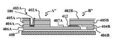
- FIGS. 1-2depict one embodiment of a solar cell with a plurality of vias.
- First and second device cells A′′, B′′are assembled from pre-cut device layers 402 A, 402 B, insulating layers 404 A, 404 B and back plane layers 406 A, 406 B and attached to a carrier substrate 408 .
- Insulated electrical contacts 403 Amake electrical contact through the device layers 402 A, a bottom electrode 405 A and the insulating layer 406 A as shown in FIG. 1 .
- Front edges of the insulating layer 404 B and back plane 406 B of module B′′are cut back (or formed in this configuration) with respect to the device layer 402 B.
- a back edge of the back plane 406 A of cell A′′extends beyond the back edges of the device layer 402 A and insulating layer 404 A.
- the device layer 402 B of cell B′′overlaps the back plane 406 A of module A′′.
- a ridge of conductive adhesive 412 on an exposed portion 407 A of the back plane 406 Amakes electrical contact with an exposed portion of a bottom electrode 405 B of the device layer 402 B as shown in FIG. 1 .
- the connection at 412can optionally be formed by other methods such as but not limited to soldering or the like.
- somemay remove the element 412 and form the connection by welding such as but not limited to laser welding, ultrasonic welding, spot welding, or other electrical joining techniques.
- Some embodimentsmay weld from the backside of cells, through the layer to create the joint between the cells at where reference 412 number is located.
- FIG. 1shows that the via is partially filled by the material 100 such as but not limited to a conductive ink.
- the dried inkis then irradiated with a pulsed laser or other rapid heating to create the connection.
- This embodiment of the inventionalso eliminates the need for a coating or other surface treatment to be applied to the metal foil.
- FIG. 2shows that optionally, the rest of the via can be filled with other conductive material 110 which is the same or different from that used in material 100 .
- the absorber layer in solar cell 10may be an absorber layer comprised of silicon, amorphous silicon, copper-indium-gallium-selenium (for CIGS solar cells), CdSe, CdTe, Cu(In,Ga)(S,Se) 2 , Cu(In,Ga,Al)(S,Se,Te) 2 , Cu—In, In—Ga, Cu—Ga, Cu—In—Ga, Cu—In—Ga—S, Cu—In—Ga—Se, other absorber materials, II-VI materials, IB-VI materials, CuZnTe, CuTe, ZnTe, IB-IIB-IVA-VIA absorbers, or other alloys, other absorber materials, IB-IIB-IVA-VIA absorber solar cells, or other alloys and/or combinations of
- the CIGS cellsmay be formed by vacuum or non-vacuum processes.
- the processesmay be one stage, two stage, or multi-stage CIGS processing techniques.
- other possible absorber layersmay be based on amorphous silicon (doped or undoped), a nanostructured layer having an inorganic porous semiconductor template with pores filled by an organic semiconductor material (see e.g., U.S.
- Patent Application Publication US 2005-0121068 A1which is incorporated herein by reference
- a polymer/blend cell architectureorganic dyes, and/or C 60 molecules, and/or other small molecules, micro-crystalline silicon cell architecture, randomly placed nanorods and/or tetrapods of inorganic materials dispersed in an organic matrix, quantum dot-based cells, or combinations of the above.
- Many of these types of cellscan be fabricated on flexible substrates.
- a size range of about 1 nm to about 200 nmshould be interpreted to include not only the explicitly recited limits of about 1 nm and about 200 nm, but also to include individual sizes such as 2 nm, 3 nm, 4 nm, and sub-ranges such as 10 nm to 50 nm, 20 nm to 100 nm, etc. . . .
Landscapes
- Photovoltaic Devices (AREA)
Abstract
Description
This application claims priority to U.S. Provisional Application Ser. No. 61/180,814 filed May 22, 2009 and fully incorporated herein by reference for all purposes.
This invention was made with Government support under Contract No. DE-FC36-07GO17047 awarded by the Department of Energy. The Government has certain rights in this invention.
This invention relates to solar cells and more specifically to back-contacted solar cells.
There is a need for an improved back-contacted solar cell with improved manufacturability.
The disadvantages associated with the prior art are overcome by embodiments of the present invention. Embodiments of the invention may be used for high throughput, high precision manufacturing for roll-to-roll production systems. The embodiments are applicable to various thin film absorbers such as but not limited to polycrystalline CIGS (copper indium gallium di-selenide, but not excluding any other of the IB, IIIA, VIA elements like e.g. aluminum, and sulfur).
In on embodiment, the vias which are a part of the metal wrap through (MWT) structure are partially filled with a silver-containing ink, and the dried (i.e. solvent-free) ink is then irradiated with a pulsed laser with sufficient energy to both fuse the silver particles and melt the aluminum foil underneath, creating an Ag—Al alloy. A pulsed laser or other energy source may be used in order to minimize any degradation of cell performance around the via. Typically the layer would be only a few microns thick, probably between 1 and 10 microns.
The technique will work with any commercial conductive adhesive, including those with polymer binders, since the organic material would be vaporized by the laser pulse. However, an especially attractive material is that marketed by Cabot Corporation, for example, which has low-melting inorganic glasses surrounding the silver particles.
A further understanding of the nature and advantages of the invention will become apparent by reference to the remaining portions of the specification and drawings.
It is to be understood that both the foregoing general description and the following detailed description are exemplary and explanatory only and are not restrictive of the invention, as claimed. It may be noted that, as used in the specification and the appended claims, the singular forms “a”, “an” and “the” include plural referents unless the context clearly dictates otherwise. Thus, for example, reference to “a material” may include mixtures of materials, reference to “a compound” may include multiple compounds, and the like. References cited herein are hereby incorporated by reference in their entirety, except to the extent that they conflict with teachings explicitly set forth in this specification.
In this specification and in the claims which follow, reference will be made to a number of terms which shall be defined to have the following meanings:
“Optional” or “optionally” means that the subsequently described circumstance may or may not occur, so that the description includes instances where the circumstance occurs and instances where it does not. For example, if a device optionally contains a feature for a barrier film, this means that the barrier film feature may or may not be present, and, thus, the description includes both structures wherein a device possesses the barrier film feature and structures wherein the barrier film feature is not present.
The vias which are a part of the metal wrap through cell structure are partially filled with a conductive ink, and the dried ink is then irradiated with a pulsed laser with sufficient energy to both fuse the solid ink components and melt the metal foil underneath, creating a metal alloy. A pulsed laser is used in order to minimize any degradation of cell performance around the via.
Typically the layer would need to be only less than 10 microns. The technique will work with any commercial conductive material, including those with organic materials, since the organic material would be vaporized by the laser pulse.
The problem with the existing methods for creating contacts to the backside electrode is that it is not easy to get a low contact resistance, and to have that interface remain stable through hot humidity aging. Most metal foils must be treated in some way, because its oxide surface makes a bad electrical contact to silver adhesives. Sn plating provides a much better interface (at some expense), but the contact resistance is still an issue, and it is desirable to make the contact area even less than at present in order to save money on silver inks.
The main improvement is provided by physically alloying the ink metal to the underlying foil (hence excellent adhesion and conductivity with no pre-treatment), and by fusing the solid particles in the ink on the surface (eliminating any organic components) so that the surface is ideally suited for good conductivity and adhesion to an overlayer of finger ink, which is expected to be another adhesive. (Contact resistance of conductive adhesives are known to be much lower on gold or silver than on any other metals.) The result is not only improved reliability and less power loss due to contact resistance, but lower materials costs since the contact can be made narrower (smaller diameter). This can be done by increasing the thickness of the secondary insulator.
Depending on the selection of materials, it may not be necessary to heat the metal foil surface to the melting point in order to get the desired level of adhesion and conduction. Also, other conducting particles may be used.
While the invention has been described and illustrated with reference to certain particular embodiments thereof, those skilled in the art will appreciate that various adaptations, changes, modifications, substitutions, deletions, or additions of procedures and protocols may be made without departing from the spirit and scope of the invention. For example, with any of the above embodiments, it should be understood that they are not limited to any one type of thin-film absorber material. They may be formed in roll to roll or in batch configuration. By way of nonlimiting example, the attachment of two metal layers is of use in embodiments such as those found in U.S. patent application Ser. No. 11/207,157. Fusing equipment may be found with reference to DELA Incorporated 175 Ward Hill Avenue Ward Hill, Mass.
Furthermore, those of skill in the art will recognize that any of the embodiments of the present invention can be applied to almost any type of solar cell material and/or architecture. For example, the absorber layer in solar cell 10 may be an absorber layer comprised of silicon, amorphous silicon, copper-indium-gallium-selenium (for CIGS solar cells), CdSe, CdTe, Cu(In,Ga)(S,Se)2, Cu(In,Ga,Al)(S,Se,Te)2, Cu—In, In—Ga, Cu—Ga, Cu—In—Ga, Cu—In—Ga—S, Cu—In—Ga—Se, other absorber materials, II-VI materials, IB-VI materials, CuZnTe, CuTe, ZnTe, IB-IIB-IVA-VIA absorbers, or other alloys, other absorber materials, IB-IIB-IVA-VIA absorber solar cells, or other alloys and/or combinations of the above, where the active materials are present in any of several forms including but not limited to bulk materials, micro-particles, nano-particles, or quantum dots. The CIGS cells may be formed by vacuum or non-vacuum processes. The processes may be one stage, two stage, or multi-stage CIGS processing techniques. Additionally, other possible absorber layers may be based on amorphous silicon (doped or undoped), a nanostructured layer having an inorganic porous semiconductor template with pores filled by an organic semiconductor material (see e.g., U.S. Patent Application Publication US 2005-0121068 A1, which is incorporated herein by reference), a polymer/blend cell architecture, organic dyes, and/or C60molecules, and/or other small molecules, micro-crystalline silicon cell architecture, randomly placed nanorods and/or tetrapods of inorganic materials dispersed in an organic matrix, quantum dot-based cells, or combinations of the above. Many of these types of cells can be fabricated on flexible substrates.
Additionally, concentrations, amounts, and other numerical data may be presented herein in a range format. It is to be understood that such range format is used merely for convenience and brevity and should be interpreted flexibly to include not only the numerical values explicitly recited as the limits of the range, but also to include all the individual numerical values or sub-ranges encompassed within that range as if each numerical value and sub-range is explicitly recited. For example, a size range of about 1 nm to about 200 nm should be interpreted to include not only the explicitly recited limits of about 1 nm and about 200 nm, but also to include individual sizes such as 2 nm, 3 nm, 4 nm, and sub-ranges such as 10 nm to 50 nm, 20 nm to 100 nm, etc. . . .
The publications discussed or cited herein are provided solely for their disclosure prior to the filing date of the present application. Nothing herein is to be construed as an admission that the present invention is not entitled to antedate such publication by virtue of prior invention. Further, the dates of publication provided may be different from the actual publication dates which may need to be independently confirmed. All publications mentioned herein are incorporated herein by reference to disclose and describe the structures and/or methods in connection with which the publications are cited.
While the above is a complete description of the preferred embodiment of the present invention, it is possible to use various alternatives, modifications and equivalents. Therefore, the scope of the present invention should be determined not with reference to the above description but should, instead, be determined with reference to the appended claims, along with their full scope of equivalents. Any feature, whether preferred or not, may be combined with any other feature, whether preferred or not. In the claims that follow, the indefinite article “A”, or “An” refers to a quantity of one or more of the item following the article, except where expressly stated otherwise. The appended claims are not to be interpreted as including means-plus-function limitations, unless such a limitation is explicitly recited in a given claim using the phrase “means for.”
Claims (17)
1. A method of solar cell manufacturing, the method comprising:
providing a photovoltaic device layer having a plurality of vias therethrough;
partially filling the vias with a liquid, electrically conductive material;
heating the liquid, electrically conductive material with sufficient energy to fuse a portion of metal foil underneath the vias with solid ink components in the liquid, electrically conductive material with the metal foil to form a metal alloy; and
filling the vias with additional electrically conductive material.
2. The method ofclaim 1 wherein solar cell has a metal wrap through (MWT) structure.
3. The method ofclaim 1 wherein the liquid, electrically conductive material comprises a silver-containing ink.
4. The method ofclaim 1 further comprising drying the liquid, electrically conductive material to make the material solvent-free.
5. The method ofclaim 1 wherein heating comprises irradiating with a pulsed laser with sufficient energy.
6. The method ofclaim 1 wherein solid ink components comprises silver particles.
7. The method ofclaim 1 wherein the metal foil comprises aluminum foil underneath.
8. The method ofclaim 1 wherein solid ink components comprises silver particles and the metal foil comprises aluminum foil underneath, creating an Ag—Al alloy.
9. The method ofclaim 1 heating comprises using a pulsed laser.
10. The method ofclaim 1 wherein partially filling forms a layer with a thickness between 1 and 10 microns in the vias.
11. The method ofclaim 1 wherein the liquid, electrically conductive material comprises conductive adhesive with polymer binder.
12. The method ofclaim 1 wherein organic material in the liquid, electrically conductive material is vaporized during heating.
13. The method ofclaim 1 the liquid, electrically conductive material comprises inorganic glasses surrounding silver particles.
14. The method ofclaim 1 comprises alloying metal in the liquid, electrically conductive material to the metal foil.
15. The method ofclaim 1 comprises fusing solid particles in solid ink components.
16. The method ofclaim 1 comprises no pre-treatment of the metal foil to remove oxides.
17. The method ofclaim 1 wherein fully filling the vias uses an electrically conductive material different from the liquid, electrically conductive material.
Priority Applications (1)
| Application Number | Priority Date | Filing Date | Title |
|---|---|---|---|
| US12/786,396US8247243B2 (en) | 2009-05-22 | 2010-05-24 | Solar cell interconnection |
Applications Claiming Priority (2)
| Application Number | Priority Date | Filing Date | Title |
|---|---|---|---|
| US18081409P | 2009-05-22 | 2009-05-22 | |
| US12/786,396US8247243B2 (en) | 2009-05-22 | 2010-05-24 | Solar cell interconnection |
Publications (2)
| Publication Number | Publication Date |
|---|---|
| US20110092014A1 US20110092014A1 (en) | 2011-04-21 |
| US8247243B2true US8247243B2 (en) | 2012-08-21 |
Family
ID=43879614
Family Applications (1)
| Application Number | Title | Priority Date | Filing Date |
|---|---|---|---|
| US12/786,396Expired - Fee RelatedUS8247243B2 (en) | 2009-05-22 | 2010-05-24 | Solar cell interconnection |
Country Status (1)
| Country | Link |
|---|---|
| US (1) | US8247243B2 (en) |
Cited By (3)
| Publication number | Priority date | Publication date | Assignee | Title |
|---|---|---|---|---|
| US9401438B2 (en) | 2013-11-13 | 2016-07-26 | Industrial Technology Research Institute | Solar cell module and solar cell thereof |
| US20170373262A1 (en)* | 2014-12-23 | 2017-12-28 | Stichting Energieonderzoek Centrum Nederland | Method of making a current collecting grid for solar cells |
| US10096726B2 (en) | 2015-06-09 | 2018-10-09 | Space Systems/Loral, Llc | All front contact solar cell |
Families Citing this family (3)
| Publication number | Priority date | Publication date | Assignee | Title |
|---|---|---|---|---|
| US9812592B2 (en)* | 2012-12-21 | 2017-11-07 | Sunpower Corporation | Metal-foil-assisted fabrication of thin-silicon solar cell |
| KR20150039536A (en)* | 2013-10-02 | 2015-04-10 | 엘지이노텍 주식회사 | Solar cell |
| EP2993210A1 (en) | 2014-09-03 | 2016-03-09 | Specialized Technology Resources Espana, S.A. | Encapsulating film for a photovoltaic module |
Citations (160)
| Publication number | Priority date | Publication date | Assignee | Title |
|---|---|---|---|---|
| US3423301A (en) | 1964-11-02 | 1969-01-21 | Monsanto Co | Electrolytic production of high-purity gallium |
| US3586541A (en) | 1966-04-21 | 1971-06-22 | Ncr Co | Photosensitive devices comprising aluminum foil |
| US3818324A (en) | 1971-04-19 | 1974-06-18 | Schlumberger Technology Corp | Well logging pad having a flexible electrode structure |
| US3903428A (en) | 1973-12-28 | 1975-09-02 | Hughes Aircraft Co | Solar cell contact design |
| US3903427A (en) | 1973-12-28 | 1975-09-02 | Hughes Aircraft Co | Solar cell connections |
| US3966568A (en) | 1974-10-21 | 1976-06-29 | Cominco Ltd. | Electrowinning of gallium |
| US3966499A (en) | 1972-10-11 | 1976-06-29 | The United States Of America As Represented By The Administrator, National Aeronautics And Space Administration | Solar cell grid patterns |
| DE2741954A1 (en) | 1977-09-17 | 1979-03-29 | Karl Hertel | Solar cell prodn. - by depositing semiconductor pn junctions in anodised aluminium pores during electron beam irradiation |
| US4191794A (en) | 1978-05-11 | 1980-03-04 | Westinghouse Electric Corp. | Integrated solar cell array |
| US4192721A (en) | 1979-04-24 | 1980-03-11 | Baranski Andrzej S | Method for producing a smooth coherent film of a metal chalconide |
| US4227942A (en) | 1979-04-23 | 1980-10-14 | General Electric Company | Photovoltaic semiconductor devices and methods of making same |
| US4243432A (en) | 1978-09-25 | 1981-01-06 | Photon Power, Inc. | Solar cell array |
| US4404422A (en) | 1980-09-26 | 1983-09-13 | Unisearch Limited | High efficiency solar cell structure |
| US4485264A (en) | 1982-11-09 | 1984-11-27 | Energy Conversion Devices, Inc. | Isolation layer for photovoltaic device and method of producing same |
| US4499658A (en) | 1983-09-06 | 1985-02-19 | Atlantic Richfield Company | Solar cell laminates |
| US4522663A (en) | 1980-09-09 | 1985-06-11 | Sovonics Solar Systems | Method for optimizing photoresponsive amorphous alloys and devices |
| US4536607A (en) | 1984-03-01 | 1985-08-20 | Wiesmann Harold J | Photovoltaic tandem cell |
| US4559924A (en) | 1979-11-20 | 1985-12-24 | The United States Of America As Represented By The United States Department Of Energy | Thin film absorber for a solar collector |
| US4574160A (en) | 1984-09-28 | 1986-03-04 | The Standard Oil Company | Flexible, rollable photovoltaic cell module |
| US4622432A (en) | 1983-04-29 | 1986-11-11 | Semiconductor Energy Laboratory Co., Ltd. | Photoelectric conversion device |
| US4642140A (en) | 1985-04-30 | 1987-02-10 | The United States Of America As Represented By The United States Department Of Energy | Process for producing chalcogenide semiconductors |
| US4677250A (en) | 1985-10-30 | 1987-06-30 | Astrosystems, Inc. | Fault tolerant thin-film photovoltaic cell |
| US4755475A (en) | 1986-02-18 | 1988-07-05 | Sanyo Electric Co., Ltd. | Method of manufacturing photovoltaic device |
| US4773944A (en) | 1987-09-08 | 1988-09-27 | Energy Conversion Devices, Inc. | Large area, low voltage, high current photovoltaic modules and method of fabricating same |
| US4786607A (en) | 1985-08-24 | 1988-11-22 | Semiconductor Energy Laboratory Co., Ltd. | Method for manufacturing a semiconductor device free from current leakage through a semiconductor layer |
| US4806436A (en) | 1984-08-06 | 1989-02-21 | Showa Aluminum Corporation | Substrate for amorphous silicon solar cells |
| US4849029A (en) | 1988-02-29 | 1989-07-18 | Chronar Corp. | Energy conversion structures |
| US4860509A (en) | 1987-05-18 | 1989-08-29 | Laaly Heshmat O | Photovoltaic cells in combination with single ply roofing membranes |
| US4865999A (en) | 1987-07-08 | 1989-09-12 | Glasstech Solar, Inc. | Solar cell fabrication method |
| US4872925A (en) | 1987-10-29 | 1989-10-10 | Glasstech, Inc. | Photovoltaic cell fabrication method and panel made thereby |
| CN1036298A (en) | 1988-02-19 | 1989-10-11 | 三洋电机株式会社 | Photovaltaic device and manufacture method thereof |
| US4940604A (en) | 1987-09-04 | 1990-07-10 | Matsushita Electric Industrial Co., Ltd. | Method for production of copper indium diselenide |
| US4981525A (en) | 1988-02-19 | 1991-01-01 | Sanyo Electric Co., Ltd. | Photovoltaic device |
| US5045409A (en) | 1987-11-27 | 1991-09-03 | Atlantic Richfield Company | Process for making thin film solar cell |
| US5057163A (en) | 1988-05-04 | 1991-10-15 | Astropower, Inc. | Deposited-silicon film solar cell |
| US5078804A (en) | 1989-06-27 | 1992-01-07 | The Boeing Company | I-III-VI2 based solar cell utilizing the structure CuInGaSe2 CdZnS/ZnO |
| US5093453A (en) | 1989-12-12 | 1992-03-03 | Administrator Of The National Aeronautics And Space Administration | Aromatic polyimides containing a dimethylsilane-linked dianhydride |
| US5139959A (en) | 1992-01-21 | 1992-08-18 | Motorola, Inc. | Method for forming bipolar transistor input protection |
| US5141564A (en) | 1988-05-03 | 1992-08-25 | The Boeing Company | Mixed ternary heterojunction solar cell |
| US5244509A (en) | 1990-08-09 | 1993-09-14 | Canon Kabushiki Kaisha | Substrate having an uneven surface for solar cell and a solar cell provided with said substrate |
| US5254179A (en) | 1991-02-21 | 1993-10-19 | Solems S.A. | Photovoltaic device and solar module having a partial transparency |
| US5268037A (en) | 1992-05-21 | 1993-12-07 | United Solar Systems Corporation | Monolithic, parallel connected photovoltaic array and method for its manufacture |
| US5277786A (en) | 1991-02-20 | 1994-01-11 | Canon Kabushiki Kaisha | Process for producing a defect-free photoelectric conversion device |
| US5286306A (en) | 1992-02-07 | 1994-02-15 | Shalini Menezes | Thin film photovoltaic cells from I-III-VI-VII compounds |
| US5356839A (en) | 1993-04-12 | 1994-10-18 | Midwest Research Institute | Enhanced quality thin film Cu(In,Ga)Se2 for semiconductor device applications by vapor-phase recrystallization |
| US5401573A (en) | 1992-11-30 | 1995-03-28 | Mcdonnell Douglas Corporation | Protection of thermal control coatings from ultraviolet radiation |
| US5419781A (en) | 1981-11-04 | 1995-05-30 | Kanegafuchi Kagaku Kogyo Kabushiki Kaisha | Flexible photovoltaic device |
| US5421908A (en) | 1992-12-28 | 1995-06-06 | Fuji Electric Co., Ltd. | Thin-film solar cell and method for the manufacture thereof |
| US5436204A (en) | 1993-04-12 | 1995-07-25 | Midwest Research Institute | Recrystallization method to selenization of thin-film Cu(In,Ga)Se2 for semiconductor device applications |
| US5441897A (en) | 1993-04-12 | 1995-08-15 | Midwest Research Institute | Method of fabricating high-efficiency Cu(In,Ga)(SeS)2 thin films for solar cells |
| US5468652A (en) | 1993-07-14 | 1995-11-21 | Sandia Corporation | Method of making a back contacted solar cell |
| EP0452588B1 (en) | 1990-04-18 | 1995-12-27 | Mitsubishi Denki Kabushiki Kaisha | Solar cell and method for manufacturing the same |
| US5501744A (en) | 1992-01-13 | 1996-03-26 | Photon Energy, Inc. | Photovoltaic cell having a p-type polycrystalline layer with large crystals |
| US5547516A (en) | 1995-05-15 | 1996-08-20 | Luch; Daniel | Substrate structures for integrated series connected photovoltaic arrays and process of manufacture of such arrays |
| US5558723A (en) | 1994-04-15 | 1996-09-24 | Siemens Solar Gmbh | Thin-film solar module with electrically conductive substrate and method for the manufacture thereof |
| US5578503A (en) | 1992-09-22 | 1996-11-26 | Siemens Aktiengesellschaft | Rapid process for producing a chalcopyrite semiconductor on a substrate |
| US5587264A (en) | 1989-03-16 | 1996-12-24 | Dai Nippon Printing Co. Ltd. | Electrostatic information recording medium and electrostatic information recording and reproducing method |
| US5626686A (en) | 1994-12-28 | 1997-05-06 | Fuji Electric Co. Ltd. | Thin-film solar cell and method of manufacturing the same |
| US5626688A (en) | 1994-12-01 | 1997-05-06 | Siemens Aktiengesellschaft | Solar cell with chalcopyrite absorber layer |
| US5633033A (en) | 1994-04-18 | 1997-05-27 | Matsushita Electric Industrial Co., Ltd. | Method for manufacturing chalcopyrite film |
| US5637537A (en) | 1991-06-27 | 1997-06-10 | United Solar Systems Corporation | Method of severing a thin film semiconductor device |
| US5667596A (en) | 1994-11-04 | 1997-09-16 | Canon Kabushiki Kaisha | Photovoltaic device and manufacturing method of the same |
| US5674325A (en) | 1995-06-07 | 1997-10-07 | Photon Energy, Inc. | Thin film photovoltaic device and process of manufacture |
| US5677250A (en) | 1994-10-17 | 1997-10-14 | Cooper Industries, Inc. | Low-temperature lead-free glaze for alumina ceramics |
| US5679176A (en) | 1994-11-04 | 1997-10-21 | Canon Kabushiki Kaisha | Group of solar cell elements, and solar cell module and production method thereof |
| US5681402A (en) | 1994-11-04 | 1997-10-28 | Canon Kabushiki Kaisha | Photovoltaic element |
| US5730852A (en) | 1995-09-25 | 1998-03-24 | Davis, Joseph & Negley | Preparation of cuxinygazsen (X=0-2, Y=0-2, Z=0-2, N=0-3) precursor films by electrodeposition for fabricating high efficiency solar cells |
| US5733381A (en) | 1993-12-22 | 1998-03-31 | Fuji Electric Co., Ltd. | Thin-film solar cell array and method of manufacturing same |
| US5735966A (en) | 1995-05-15 | 1998-04-07 | Luch; Daniel | Substrate structures for integrated series connected photovoltaic arrays and process of manufacture of such arrays |
| US5759291A (en) | 1995-06-28 | 1998-06-02 | Canon Kabushiki Kaisha | Photovoltaic cell and method of making the same |
| US5865904A (en) | 1995-08-21 | 1999-02-02 | Fuji Electric Co., Ltd. | Flexible photoelectric conversion module and method for its manufacture |
| US5897715A (en) | 1997-05-19 | 1999-04-27 | Midwest Research Institute | Interdigitated photovoltaic power conversion device |
| US5925228A (en) | 1997-01-09 | 1999-07-20 | Sandia Corporation | Electrophoretically active sol-gel processes to backfill, seal, and/or densify porous, flawed, and/or cracked coatings on electrically conductive material |
| US5951786A (en) | 1997-12-19 | 1999-09-14 | Sandia Corporation | Laminated photovoltaic modules using back-contact solar cells |
| US5985691A (en) | 1997-05-16 | 1999-11-16 | International Solar Electric Technology, Inc. | Method of making compound semiconductor films and making related electronic devices |
| US5994163A (en) | 1994-10-21 | 1999-11-30 | Nordic Solar Energy Ab | Method of manufacturing thin-film solar cells |
| US6034322A (en) | 1999-07-01 | 2000-03-07 | Space Systems/Loral, Inc. | Solar cell assembly |
| US6034810A (en) | 1997-04-18 | 2000-03-07 | Memsolutions, Inc. | Field emission charge controlled mirror (FEA-CCM) |
| US6083801A (en) | 1997-02-10 | 2000-07-04 | Semiconductor Energy Laboratory Co., Ltd. | Manufacturing method of semiconductor and manufacturing method of semiconductor device |
| US6107562A (en) | 1998-03-24 | 2000-08-22 | Matsushita Electric Industrial Co., Ltd. | Semiconductor thin film, method for manufacturing the same, and solar cell using the same |
| US6121541A (en) | 1997-07-28 | 2000-09-19 | Bp Solarex | Monolithic multi-junction solar cells with amorphous silicon and CIS and their alloys |
| US6124039A (en) | 1996-04-03 | 2000-09-26 | Alusuisse Technology & Management Ltd. | Coating substrate |
| US6127202A (en) | 1998-07-02 | 2000-10-03 | International Solar Electronic Technology, Inc. | Oxide-based method of making compound semiconductor films and making related electronic devices |
| US6130465A (en) | 1997-10-29 | 2000-10-10 | Light Point Systems Inc. | Micro-solar assembly |
| US6201181B1 (en) | 1998-12-08 | 2001-03-13 | Ase Americas, Inc. | Portable solar module cart |
| US6239352B1 (en) | 1999-03-30 | 2001-05-29 | Daniel Luch | Substrate and collector grid structures for electrically interconnecting photovoltaic arrays and process of manufacture of such arrays |
| US6265652B1 (en) | 1995-06-15 | 2001-07-24 | Kanegafuchi Kagaku Kogyo Kabushiki Kabushiki Kaisha | Integrated thin-film solar battery and method of manufacturing the same |
| US6268014B1 (en) | 1997-10-02 | 2001-07-31 | Chris Eberspacher | Method for forming solar cell materials from particulars |
| US20010020486A1 (en) | 2000-02-21 | 2001-09-13 | Sanyo Electric Co., Ltd. | Solar cell module |
| US6333206B1 (en) | 1996-12-24 | 2001-12-25 | Nitto Denko Corporation | Process for the production of semiconductor device |
| US6359209B1 (en) | 2000-02-23 | 2002-03-19 | Hughes Electronics Corporation | Solar panel and solar cell having in-plane solar cell interconnect with integrated diode tab |
| US6372538B1 (en) | 2000-03-16 | 2002-04-16 | University Of Delaware | Fabrication of thin-film, flexible photovoltaic module |
| US6455347B1 (en) | 1999-06-14 | 2002-09-24 | Kaneka Corporation | Method of fabricating thin-film photovoltaic module |
| US6459032B1 (en) | 1995-05-15 | 2002-10-01 | Daniel Luch | Substrate structures for integrated series connected photovoltaic arrays and process of manufacture of such arrays |
| US6468828B1 (en) | 1998-07-14 | 2002-10-22 | Sky Solar L.L.C. | Method of manufacturing lightweight, high efficiency photovoltaic module |
| US20020189662A1 (en) | 1999-12-02 | 2002-12-19 | Holger Lomparski | Device for producing solar energy and water |
| WO2003007386A1 (en) | 2001-07-13 | 2003-01-23 | Midwest Research Institute | Thin-film solar cell fabricated on a flexible metallic substrate |
| US6511861B2 (en) | 1997-12-26 | 2003-01-28 | Canon Kabushiki Kaisha | Method of producing photovoltaic element module |
| US6553729B1 (en) | 2000-06-09 | 2003-04-29 | United Solar Systems Corporation | Self-adhesive photovoltaic module |
| WO2003001602A3 (en) | 2001-06-21 | 2003-05-01 | Akzo Nobel Nv | Manufacturing a solar cell foil connected in series via a temporary substrate |
| US6573445B1 (en) | 1998-11-23 | 2003-06-03 | Stichting Energieonderzoek Centrum Nederland | Method for manufacturing a metallization pattern on a photovoltaic cell |
| US20030103181A1 (en) | 2001-12-03 | 2003-06-05 | Hitachi, Ltd. | Liquid crystal display device |
| US20030198587A1 (en) | 1999-02-12 | 2003-10-23 | Gelest, Inc. | Method for low-temperature organic chemical vapor deposition of tungsten nitride, tungsten nitride films and tungsten nitride diffusion barriers for computer interconnect metallization |
| US20030205270A1 (en) | 2001-09-20 | 2003-11-06 | Stanbery Billy J. | Compositions including a collection layer |
| US20030227021A1 (en) | 2002-06-07 | 2003-12-11 | Semiconductor Energy Laboratory Co., Ltd. | Light emitting device and manufacturing method thereof |
| US20040069340A1 (en) | 1999-03-30 | 2004-04-15 | Daniel Luch | Substrate and collector grid structures for integrated series connected photovoltaic arrays and process of manufacture of such arrays |
| US6729081B2 (en) | 2000-06-09 | 2004-05-04 | United Solar Systems Corporation | Self-adhesive photovoltaic module |
| US6750662B1 (en) | 1999-10-04 | 2004-06-15 | Stichting Energieonderzoek Centrum Nederland | Apparatus for localizing production errors in a photovoltaic element |
| US20040144419A1 (en) | 2001-01-31 | 2004-07-29 | Renaud Fix | Transparent substrate equipped with an electrode |
| US6774497B1 (en) | 2003-03-28 | 2004-08-10 | Freescale Semiconductor, Inc. | Flip-chip assembly with thin underfill and thick solder mask |
| US6787405B2 (en) | 2002-09-03 | 2004-09-07 | Toppoly Optoelectronics Corp. | Method of fabricating liquid crystal display devices integrated with driving circuit |
| US20040187917A1 (en) | 2003-03-29 | 2004-09-30 | Nanosolar, Inc. | Transparent electrode, optoelectronic apparatus and devices |
| US6803513B2 (en) | 2002-08-20 | 2004-10-12 | United Solar Systems Corporation | Series connected photovoltaic module and method for its manufacture |
| US20040214409A1 (en) | 1991-06-04 | 2004-10-28 | Warren Farnworth | Method and apparatus for manufacturing known good semiconductor die |
| US20040219730A1 (en) | 2001-04-16 | 2004-11-04 | Basol Bulent M. | Method of forming semiconductor compound film for fabrication of electronic device and film produced by same |
| WO2004100244A1 (en) | 2003-05-07 | 2004-11-18 | Universität Konstanz | Method for texturing surfaces of silicon wafers |
| US20040261840A1 (en) | 2003-06-30 | 2004-12-30 | Advent Solar, Inc. | Emitter wrap-through back contact solar cells on thin silicon wafers |
| US20040261839A1 (en) | 2003-06-26 | 2004-12-30 | Gee James M | Fabrication of back-contacted silicon solar cells using thermomigration to create conductive vias |
| US20050006714A1 (en) | 2000-07-28 | 2005-01-13 | Michael Graetzel | Solid state heterojunction and solid state sensitized photovoltaic cell |
| US6846696B2 (en) | 2001-05-22 | 2005-01-25 | Semiconductor Energy Laboratory Co., Ltd. | Method for manufacturing solar battery |
| US20050061363A1 (en) | 2003-09-23 | 2005-03-24 | Ginley David S. | Organic solar cells including group IV nanocrystals and method of manufacture |
| US20050072457A1 (en) | 2003-10-02 | 2005-04-07 | Glenn Gregory S. | Solar cell structure with integrated discrete by-pass diode |
| US20050087225A1 (en) | 2002-01-10 | 2005-04-28 | Tdk Corporation | Photovoltaic device |
| US20050109392A1 (en) | 2002-09-30 | 2005-05-26 | Hollars Dennis R. | Manufacturing apparatus and method for large-scale production of thin-film solar cells |
| US20050117194A1 (en) | 2003-10-14 | 2005-06-02 | Sang-Ho Kim | Method for preparing electrode system, electrode system prepared therefrom, and electric device comprising the same |
| US20050126621A1 (en) | 2003-08-20 | 2005-06-16 | Powerlight Corporation | PV wind performance enhancing methods and apparatus |
| US20050135724A1 (en) | 2003-12-19 | 2005-06-23 | Henry Helvajian | Integrated glass ceramic systems |
| US20050176270A1 (en) | 2004-02-11 | 2005-08-11 | Daniel Luch | Methods and structures for the production of electrically treated items and electrical connections |
| US20050172998A1 (en) | 2004-02-05 | 2005-08-11 | Advent Solar, Inc. | Buried-contact solar cells with self-doping contacts |
| US20050172996A1 (en) | 2004-02-05 | 2005-08-11 | Advent Solar, Inc. | Contact fabrication of emitter wrap-through back contact silicon solar cells |
| US20050175856A1 (en) | 2002-06-06 | 2005-08-11 | Jonathan Rogers | Electroluminescent device |
| US20050176164A1 (en) | 2004-02-05 | 2005-08-11 | Advent Solar, Inc. | Back-contact solar cells and methods for fabrication |
| US20050183767A1 (en) | 2004-02-19 | 2005-08-25 | Nanosolar, Inc. | Solution-based fabrication of photovoltaic cell |
| US20050186342A1 (en) | 2004-02-19 | 2005-08-25 | Nanosolar, Inc. | Formation of CIGS absorber layer materials using atomic layer deposition and high throughput surface treatment |
| US20050217719A1 (en) | 2002-06-04 | 2005-10-06 | Mahieu Danny R | Method and apparatus for filling a dye sensitized solar cell with electrolyte |
| US20050241692A1 (en) | 2002-08-29 | 2005-11-03 | Rubin Leonid B | Electrode for photovoltaic cells, photovoltaic cell and photovoltaic module |
| US20050263180A1 (en) | 2004-06-01 | 2005-12-01 | Alan Montello | Photovoltaic module architecture |
| US20060030141A1 (en) | 2004-08-04 | 2006-02-09 | Weng Jian-Gang | Method to form an interconnect |
| WO2006033858A1 (en) | 2004-09-18 | 2006-03-30 | Nanosolar, Inc. | Formation of solar cells on foil substrates |
| US20060107471A1 (en) | 2002-06-04 | 2006-05-25 | Martin Spath | Method and apparatus for dyeing a layer of nanocrystalline material |
| US20060118165A1 (en) | 2002-06-04 | 2006-06-08 | Van Roosmalen Johannes A M | Liquid-containing photovoltaic element |
| US20060121748A1 (en) | 2003-01-24 | 2006-06-08 | Brieko Meindert W | Coupling device for thin-film photovoltaic cells |
| US20060121701A1 (en) | 2004-03-15 | 2006-06-08 | Solopower, Inc. | Technique and apparatus for depositing layers of semiconductors for solar cell and module fabrication |
| US20060157103A1 (en)* | 2005-01-20 | 2006-07-20 | Nanosolar, Inc. | Optoelectronic architecture having compound conducting substrate cross-reference to related application |
| US20060160261A1 (en)* | 2005-01-20 | 2006-07-20 | Nanosolar, Inc. | Series interconnected optoelectronic device module assembly |
| US20060180195A1 (en) | 1999-03-30 | 2006-08-17 | Daniel Luch | Substrate and collector grid structures for integrated photovoltaic arrays and process of manufacture of such arrays |
| US7122398B1 (en) | 2004-03-25 | 2006-10-17 | Nanosolar, Inc. | Manufacturing of optoelectronic devices |
| US20070000537A1 (en)* | 2004-09-18 | 2007-01-04 | Craig Leidholm | Formation of solar cells with conductive barrier layers and foil substrates |
| US20070186971A1 (en)* | 2005-01-20 | 2007-08-16 | Nanosolar, Inc. | High-efficiency solar cell with insulated vias |
| US20070283996A1 (en) | 2006-06-13 | 2007-12-13 | Miasole | Photovoltaic module with insulating interconnect carrier |
| US20070283997A1 (en) | 2006-06-13 | 2007-12-13 | Miasole | Photovoltaic module with integrated current collection and interconnection |
| US20080011350A1 (en) | 1999-03-30 | 2008-01-17 | Daniel Luch | Collector grid, electrode structures and interconnect structures for photovoltaic arrays and other optoelectric devices |
| US20080053519A1 (en) | 2006-08-30 | 2008-03-06 | Miasole | Laminated photovoltaic cell |
| US20080227236A1 (en) | 1995-05-15 | 2008-09-18 | Daniel Luch | Substrate structures for integrated series connected photovoltaic arrays and process of manufacture of such arrays |
| US20080314433A1 (en) | 1995-05-15 | 2008-12-25 | Daniel Luch | Substrate structures for integrated series connected photovoltaic arrays and process of manufacture of such arrays |
| US7507971B2 (en) | 2003-04-11 | 2009-03-24 | Hamamatsu Photonics K.K. | Radioactive ray detector |
| US20090107538A1 (en) | 2007-10-29 | 2009-04-30 | Daniel Luch | Collector grid and interconnect structures for photovoltaic arrays and modules |
| US20090111206A1 (en) | 1999-03-30 | 2009-04-30 | Daniel Luch | Collector grid, electrode structures and interrconnect structures for photovoltaic arrays and methods of manufacture |
| US7898053B2 (en) | 2000-02-04 | 2011-03-01 | Daniel Luch | Substrate structures for integrated series connected photovoltaic arrays and process of manufacture of such arrays |
| US7898054B2 (en) | 2000-02-04 | 2011-03-01 | Daniel Luch | Substrate structures for integrated series connected photovoltaic arrays and process of manufacture of such arrays |
Family Cites Families (2)
| Publication number | Priority date | Publication date | Assignee | Title |
|---|---|---|---|---|
| US6681592B1 (en)* | 2001-02-16 | 2004-01-27 | Hamilton Sundstrand Corporation | Electrically driven aircraft cabin ventilation and environmental control system |
| US6946597B2 (en)* | 2002-06-22 | 2005-09-20 | Nanosular, Inc. | Photovoltaic devices fabricated by growth from porous template |
- 2010
- 2010-05-24USUS12/786,396patent/US8247243B2/ennot_activeExpired - Fee Related
Patent Citations (185)
| Publication number | Priority date | Publication date | Assignee | Title |
|---|---|---|---|---|
| US3423301A (en) | 1964-11-02 | 1969-01-21 | Monsanto Co | Electrolytic production of high-purity gallium |
| US3586541A (en) | 1966-04-21 | 1971-06-22 | Ncr Co | Photosensitive devices comprising aluminum foil |
| US3818324A (en) | 1971-04-19 | 1974-06-18 | Schlumberger Technology Corp | Well logging pad having a flexible electrode structure |
| US3966499A (en) | 1972-10-11 | 1976-06-29 | The United States Of America As Represented By The Administrator, National Aeronautics And Space Administration | Solar cell grid patterns |
| US3903428A (en) | 1973-12-28 | 1975-09-02 | Hughes Aircraft Co | Solar cell contact design |
| US3903427A (en) | 1973-12-28 | 1975-09-02 | Hughes Aircraft Co | Solar cell connections |
| US3966568A (en) | 1974-10-21 | 1976-06-29 | Cominco Ltd. | Electrowinning of gallium |
| DE2741954A1 (en) | 1977-09-17 | 1979-03-29 | Karl Hertel | Solar cell prodn. - by depositing semiconductor pn junctions in anodised aluminium pores during electron beam irradiation |
| US4191794A (en) | 1978-05-11 | 1980-03-04 | Westinghouse Electric Corp. | Integrated solar cell array |
| US4243432A (en) | 1978-09-25 | 1981-01-06 | Photon Power, Inc. | Solar cell array |
| US4227942A (en) | 1979-04-23 | 1980-10-14 | General Electric Company | Photovoltaic semiconductor devices and methods of making same |
| US4192721A (en) | 1979-04-24 | 1980-03-11 | Baranski Andrzej S | Method for producing a smooth coherent film of a metal chalconide |
| US4559924A (en) | 1979-11-20 | 1985-12-24 | The United States Of America As Represented By The United States Department Of Energy | Thin film absorber for a solar collector |
| US4522663A (en) | 1980-09-09 | 1985-06-11 | Sovonics Solar Systems | Method for optimizing photoresponsive amorphous alloys and devices |
| US4404422A (en) | 1980-09-26 | 1983-09-13 | Unisearch Limited | High efficiency solar cell structure |
| US5419781A (en) | 1981-11-04 | 1995-05-30 | Kanegafuchi Kagaku Kogyo Kabushiki Kaisha | Flexible photovoltaic device |
| US4485264A (en) | 1982-11-09 | 1984-11-27 | Energy Conversion Devices, Inc. | Isolation layer for photovoltaic device and method of producing same |
| US4622432A (en) | 1983-04-29 | 1986-11-11 | Semiconductor Energy Laboratory Co., Ltd. | Photoelectric conversion device |
| US4499658A (en) | 1983-09-06 | 1985-02-19 | Atlantic Richfield Company | Solar cell laminates |
| US4536607A (en) | 1984-03-01 | 1985-08-20 | Wiesmann Harold J | Photovoltaic tandem cell |
| US4806436A (en) | 1984-08-06 | 1989-02-21 | Showa Aluminum Corporation | Substrate for amorphous silicon solar cells |
| US4574160A (en) | 1984-09-28 | 1986-03-04 | The Standard Oil Company | Flexible, rollable photovoltaic cell module |
| US4642140A (en) | 1985-04-30 | 1987-02-10 | The United States Of America As Represented By The United States Department Of Energy | Process for producing chalcogenide semiconductors |
| US4786607A (en) | 1985-08-24 | 1988-11-22 | Semiconductor Energy Laboratory Co., Ltd. | Method for manufacturing a semiconductor device free from current leakage through a semiconductor layer |
| US4677250A (en) | 1985-10-30 | 1987-06-30 | Astrosystems, Inc. | Fault tolerant thin-film photovoltaic cell |
| US4755475A (en) | 1986-02-18 | 1988-07-05 | Sanyo Electric Co., Ltd. | Method of manufacturing photovoltaic device |
| US4860509A (en) | 1987-05-18 | 1989-08-29 | Laaly Heshmat O | Photovoltaic cells in combination with single ply roofing membranes |
| US4865999A (en) | 1987-07-08 | 1989-09-12 | Glasstech Solar, Inc. | Solar cell fabrication method |
| US4940604A (en) | 1987-09-04 | 1990-07-10 | Matsushita Electric Industrial Co., Ltd. | Method for production of copper indium diselenide |
| US4773944A (en) | 1987-09-08 | 1988-09-27 | Energy Conversion Devices, Inc. | Large area, low voltage, high current photovoltaic modules and method of fabricating same |
| US4872925A (en) | 1987-10-29 | 1989-10-10 | Glasstech, Inc. | Photovoltaic cell fabrication method and panel made thereby |
| US5045409A (en) | 1987-11-27 | 1991-09-03 | Atlantic Richfield Company | Process for making thin film solar cell |
| CN1036298A (en) | 1988-02-19 | 1989-10-11 | 三洋电机株式会社 | Photovaltaic device and manufacture method thereof |
| US4981525A (en) | 1988-02-19 | 1991-01-01 | Sanyo Electric Co., Ltd. | Photovoltaic device |
| US4849029A (en) | 1988-02-29 | 1989-07-18 | Chronar Corp. | Energy conversion structures |
| US5141564A (en) | 1988-05-03 | 1992-08-25 | The Boeing Company | Mixed ternary heterojunction solar cell |
| US5057163A (en) | 1988-05-04 | 1991-10-15 | Astropower, Inc. | Deposited-silicon film solar cell |
| US5587264A (en) | 1989-03-16 | 1996-12-24 | Dai Nippon Printing Co. Ltd. | Electrostatic information recording medium and electrostatic information recording and reproducing method |
| US5078804A (en) | 1989-06-27 | 1992-01-07 | The Boeing Company | I-III-VI2 based solar cell utilizing the structure CuInGaSe2 CdZnS/ZnO |
| US5093453A (en) | 1989-12-12 | 1992-03-03 | Administrator Of The National Aeronautics And Space Administration | Aromatic polyimides containing a dimethylsilane-linked dianhydride |
| EP0452588B1 (en) | 1990-04-18 | 1995-12-27 | Mitsubishi Denki Kabushiki Kaisha | Solar cell and method for manufacturing the same |
| US5244509A (en) | 1990-08-09 | 1993-09-14 | Canon Kabushiki Kaisha | Substrate having an uneven surface for solar cell and a solar cell provided with said substrate |
| US5277786A (en) | 1991-02-20 | 1994-01-11 | Canon Kabushiki Kaisha | Process for producing a defect-free photoelectric conversion device |
| US5254179A (en) | 1991-02-21 | 1993-10-19 | Solems S.A. | Photovoltaic device and solar module having a partial transparency |
| US20040214409A1 (en) | 1991-06-04 | 2004-10-28 | Warren Farnworth | Method and apparatus for manufacturing known good semiconductor die |
| US5637537A (en) | 1991-06-27 | 1997-06-10 | United Solar Systems Corporation | Method of severing a thin film semiconductor device |
| US5501744A (en) | 1992-01-13 | 1996-03-26 | Photon Energy, Inc. | Photovoltaic cell having a p-type polycrystalline layer with large crystals |
| US5139959A (en) | 1992-01-21 | 1992-08-18 | Motorola, Inc. | Method for forming bipolar transistor input protection |
| US5286306A (en) | 1992-02-07 | 1994-02-15 | Shalini Menezes | Thin film photovoltaic cells from I-III-VI-VII compounds |
| US5268037A (en) | 1992-05-21 | 1993-12-07 | United Solar Systems Corporation | Monolithic, parallel connected photovoltaic array and method for its manufacture |
| US5578503A (en) | 1992-09-22 | 1996-11-26 | Siemens Aktiengesellschaft | Rapid process for producing a chalcopyrite semiconductor on a substrate |
| US5401573A (en) | 1992-11-30 | 1995-03-28 | Mcdonnell Douglas Corporation | Protection of thermal control coatings from ultraviolet radiation |
| US5421908A (en) | 1992-12-28 | 1995-06-06 | Fuji Electric Co., Ltd. | Thin-film solar cell and method for the manufacture thereof |
| US5356839A (en) | 1993-04-12 | 1994-10-18 | Midwest Research Institute | Enhanced quality thin film Cu(In,Ga)Se2 for semiconductor device applications by vapor-phase recrystallization |
| US5441897A (en) | 1993-04-12 | 1995-08-15 | Midwest Research Institute | Method of fabricating high-efficiency Cu(In,Ga)(SeS)2 thin films for solar cells |
| US5436204A (en) | 1993-04-12 | 1995-07-25 | Midwest Research Institute | Recrystallization method to selenization of thin-film Cu(In,Ga)Se2 for semiconductor device applications |
| US5468652A (en) | 1993-07-14 | 1995-11-21 | Sandia Corporation | Method of making a back contacted solar cell |
| US5733381A (en) | 1993-12-22 | 1998-03-31 | Fuji Electric Co., Ltd. | Thin-film solar cell array and method of manufacturing same |
| US5928439A (en) | 1993-12-22 | 1999-07-27 | Fuji Electric Co. Ltd. | Thin-film solar cell and method for the manufacture thereof |
| US5558723A (en) | 1994-04-15 | 1996-09-24 | Siemens Solar Gmbh | Thin-film solar module with electrically conductive substrate and method for the manufacture thereof |
| US5633033A (en) | 1994-04-18 | 1997-05-27 | Matsushita Electric Industrial Co., Ltd. | Method for manufacturing chalcopyrite film |
| US5677250A (en) | 1994-10-17 | 1997-10-14 | Cooper Industries, Inc. | Low-temperature lead-free glaze for alumina ceramics |
| US5994163A (en) | 1994-10-21 | 1999-11-30 | Nordic Solar Energy Ab | Method of manufacturing thin-film solar cells |
| US5667596A (en) | 1994-11-04 | 1997-09-16 | Canon Kabushiki Kaisha | Photovoltaic device and manufacturing method of the same |
| US5679176A (en) | 1994-11-04 | 1997-10-21 | Canon Kabushiki Kaisha | Group of solar cell elements, and solar cell module and production method thereof |
| US5681402A (en) | 1994-11-04 | 1997-10-28 | Canon Kabushiki Kaisha | Photovoltaic element |
| US5626688A (en) | 1994-12-01 | 1997-05-06 | Siemens Aktiengesellschaft | Solar cell with chalcopyrite absorber layer |
| US5626686A (en) | 1994-12-28 | 1997-05-06 | Fuji Electric Co. Ltd. | Thin-film solar cell and method of manufacturing the same |
| US20080227236A1 (en) | 1995-05-15 | 2008-09-18 | Daniel Luch | Substrate structures for integrated series connected photovoltaic arrays and process of manufacture of such arrays |
| US5735966A (en) | 1995-05-15 | 1998-04-07 | Luch; Daniel | Substrate structures for integrated series connected photovoltaic arrays and process of manufacture of such arrays |
| US6459032B1 (en) | 1995-05-15 | 2002-10-01 | Daniel Luch | Substrate structures for integrated series connected photovoltaic arrays and process of manufacture of such arrays |
| US7732243B2 (en) | 1995-05-15 | 2010-06-08 | Daniel Luch | Substrate structures for integrated series connected photovoltaic arrays and process of manufacture of such arrays |
| US5547516A (en) | 1995-05-15 | 1996-08-20 | Luch; Daniel | Substrate structures for integrated series connected photovoltaic arrays and process of manufacture of such arrays |
| US20080314433A1 (en) | 1995-05-15 | 2008-12-25 | Daniel Luch | Substrate structures for integrated series connected photovoltaic arrays and process of manufacture of such arrays |
| US5868869A (en) | 1995-06-07 | 1999-02-09 | Photon Energy, Inc. | Thin film photovoltaic device and process of manufacture |
| US5674325A (en) | 1995-06-07 | 1997-10-07 | Photon Energy, Inc. | Thin film photovoltaic device and process of manufacture |
| US6265652B1 (en) | 1995-06-15 | 2001-07-24 | Kanegafuchi Kagaku Kogyo Kabushiki Kabushiki Kaisha | Integrated thin-film solar battery and method of manufacturing the same |
| US6437231B2 (en) | 1995-06-15 | 2002-08-20 | Kanegafuchi Kagaku Kogyo Kabushiki Kaisha | Integrated thin-film solar battery and method of manufacturing the same |
| US5759291A (en) | 1995-06-28 | 1998-06-02 | Canon Kabushiki Kaisha | Photovoltaic cell and method of making the same |
| US5865904A (en) | 1995-08-21 | 1999-02-02 | Fuji Electric Co., Ltd. | Flexible photoelectric conversion module and method for its manufacture |
| US5730852A (en) | 1995-09-25 | 1998-03-24 | Davis, Joseph & Negley | Preparation of cuxinygazsen (X=0-2, Y=0-2, Z=0-2, N=0-3) precursor films by electrodeposition for fabricating high efficiency solar cells |
| US6124039A (en) | 1996-04-03 | 2000-09-26 | Alusuisse Technology & Management Ltd. | Coating substrate |
| US6333206B1 (en) | 1996-12-24 | 2001-12-25 | Nitto Denko Corporation | Process for the production of semiconductor device |
| US5925228A (en) | 1997-01-09 | 1999-07-20 | Sandia Corporation | Electrophoretically active sol-gel processes to backfill, seal, and/or densify porous, flawed, and/or cracked coatings on electrically conductive material |
| US6083801A (en) | 1997-02-10 | 2000-07-04 | Semiconductor Energy Laboratory Co., Ltd. | Manufacturing method of semiconductor and manufacturing method of semiconductor device |
| US6034810A (en) | 1997-04-18 | 2000-03-07 | Memsolutions, Inc. | Field emission charge controlled mirror (FEA-CCM) |
| US5985691A (en) | 1997-05-16 | 1999-11-16 | International Solar Electric Technology, Inc. | Method of making compound semiconductor films and making related electronic devices |
| US5897715A (en) | 1997-05-19 | 1999-04-27 | Midwest Research Institute | Interdigitated photovoltaic power conversion device |
| US6121541A (en) | 1997-07-28 | 2000-09-19 | Bp Solarex | Monolithic multi-junction solar cells with amorphous silicon and CIS and their alloys |
| US6268014B1 (en) | 1997-10-02 | 2001-07-31 | Chris Eberspacher | Method for forming solar cell materials from particulars |
| US6130465A (en) | 1997-10-29 | 2000-10-10 | Light Point Systems Inc. | Micro-solar assembly |
| US5951786A (en) | 1997-12-19 | 1999-09-14 | Sandia Corporation | Laminated photovoltaic modules using back-contact solar cells |
| US6511861B2 (en) | 1997-12-26 | 2003-01-28 | Canon Kabushiki Kaisha | Method of producing photovoltaic element module |
| US6107562A (en) | 1998-03-24 | 2000-08-22 | Matsushita Electric Industrial Co., Ltd. | Semiconductor thin film, method for manufacturing the same, and solar cell using the same |
| US6127202A (en) | 1998-07-02 | 2000-10-03 | International Solar Electronic Technology, Inc. | Oxide-based method of making compound semiconductor films and making related electronic devices |
| US6468828B1 (en) | 1998-07-14 | 2002-10-22 | Sky Solar L.L.C. | Method of manufacturing lightweight, high efficiency photovoltaic module |
| US6573445B1 (en) | 1998-11-23 | 2003-06-03 | Stichting Energieonderzoek Centrum Nederland | Method for manufacturing a metallization pattern on a photovoltaic cell |
| US6201181B1 (en) | 1998-12-08 | 2001-03-13 | Ase Americas, Inc. | Portable solar module cart |
| US20030198587A1 (en) | 1999-02-12 | 2003-10-23 | Gelest, Inc. | Method for low-temperature organic chemical vapor deposition of tungsten nitride, tungsten nitride films and tungsten nitride diffusion barriers for computer interconnect metallization |
| US20060180195A1 (en) | 1999-03-30 | 2006-08-17 | Daniel Luch | Substrate and collector grid structures for integrated photovoltaic arrays and process of manufacture of such arrays |
| US20090111206A1 (en) | 1999-03-30 | 2009-04-30 | Daniel Luch | Collector grid, electrode structures and interrconnect structures for photovoltaic arrays and methods of manufacture |
| US6239352B1 (en) | 1999-03-30 | 2001-05-29 | Daniel Luch | Substrate and collector grid structures for electrically interconnecting photovoltaic arrays and process of manufacture of such arrays |
| US20080011350A1 (en) | 1999-03-30 | 2008-01-17 | Daniel Luch | Collector grid, electrode structures and interconnect structures for photovoltaic arrays and other optoelectric devices |
| US7635810B2 (en) | 1999-03-30 | 2009-12-22 | Daniel Luch | Substrate and collector grid structures for integrated photovoltaic arrays and process of manufacture of such arrays |
| US7507903B2 (en) | 1999-03-30 | 2009-03-24 | Daniel Luch | Substrate and collector grid structures for integrated series connected photovoltaic arrays and process of manufacture of such arrays |
| US20090223552A1 (en) | 1999-03-30 | 2009-09-10 | Daniel Luch | Substrate and collector grid structures for integrated series connected photovoltaic arrays and process of manufacture of such arrays |
| US6414235B1 (en) | 1999-03-30 | 2002-07-02 | Daniel Luch | Substrate and collector grid structures for integrated series connected photovoltaic arrays and process of manufacture of such arrays |
| US20090173374A1 (en) | 1999-03-30 | 2009-07-09 | Daniel Luch | Substrate and collector grid structures for integrated series connected photovoltaic arrays and process of manufacture of such arrays |
| US20090169722A1 (en) | 1999-03-30 | 2009-07-02 | Daniel Luch | Substrate and collector grid structures for integrated series connected photovoltaic arrays and process of manufacture of such arrays |
| US20040069340A1 (en) | 1999-03-30 | 2004-04-15 | Daniel Luch | Substrate and collector grid structures for integrated series connected photovoltaic arrays and process of manufacture of such arrays |
| US20090145551A1 (en) | 1999-03-30 | 2009-06-11 | Daniel Luch | Substrate and collector grid structures for integrated series connected photovoltaic arrays and process of manufacture of such arrays |
| US6455347B1 (en) | 1999-06-14 | 2002-09-24 | Kaneka Corporation | Method of fabricating thin-film photovoltaic module |
| US6034322A (en) | 1999-07-01 | 2000-03-07 | Space Systems/Loral, Inc. | Solar cell assembly |
| US6750662B1 (en) | 1999-10-04 | 2004-06-15 | Stichting Energieonderzoek Centrum Nederland | Apparatus for localizing production errors in a photovoltaic element |
| US20020189662A1 (en) | 1999-12-02 | 2002-12-19 | Holger Lomparski | Device for producing solar energy and water |
| US7898053B2 (en) | 2000-02-04 | 2011-03-01 | Daniel Luch | Substrate structures for integrated series connected photovoltaic arrays and process of manufacture of such arrays |
| US7898054B2 (en) | 2000-02-04 | 2011-03-01 | Daniel Luch | Substrate structures for integrated series connected photovoltaic arrays and process of manufacture of such arrays |
| US20010020486A1 (en) | 2000-02-21 | 2001-09-13 | Sanyo Electric Co., Ltd. | Solar cell module |
| US6359209B1 (en) | 2000-02-23 | 2002-03-19 | Hughes Electronics Corporation | Solar panel and solar cell having in-plane solar cell interconnect with integrated diode tab |
| US6372538B1 (en) | 2000-03-16 | 2002-04-16 | University Of Delaware | Fabrication of thin-film, flexible photovoltaic module |
| US6553729B1 (en) | 2000-06-09 | 2003-04-29 | United Solar Systems Corporation | Self-adhesive photovoltaic module |
| US6729081B2 (en) | 2000-06-09 | 2004-05-04 | United Solar Systems Corporation | Self-adhesive photovoltaic module |
| US20050006714A1 (en) | 2000-07-28 | 2005-01-13 | Michael Graetzel | Solid state heterojunction and solid state sensitized photovoltaic cell |
| US20040144419A1 (en) | 2001-01-31 | 2004-07-29 | Renaud Fix | Transparent substrate equipped with an electrode |
| US20040219730A1 (en) | 2001-04-16 | 2004-11-04 | Basol Bulent M. | Method of forming semiconductor compound film for fabrication of electronic device and film produced by same |
| US6846696B2 (en) | 2001-05-22 | 2005-01-25 | Semiconductor Energy Laboratory Co., Ltd. | Method for manufacturing solar battery |
| WO2003001602A3 (en) | 2001-06-21 | 2003-05-01 | Akzo Nobel Nv | Manufacturing a solar cell foil connected in series via a temporary substrate |
| WO2003007386A1 (en) | 2001-07-13 | 2003-01-23 | Midwest Research Institute | Thin-film solar cell fabricated on a flexible metallic substrate |
| US20030205270A1 (en) | 2001-09-20 | 2003-11-06 | Stanbery Billy J. | Compositions including a collection layer |
| US20030103181A1 (en) | 2001-12-03 | 2003-06-05 | Hitachi, Ltd. | Liquid crystal display device |
| US20050087225A1 (en) | 2002-01-10 | 2005-04-28 | Tdk Corporation | Photovoltaic device |
| US20060107471A1 (en) | 2002-06-04 | 2006-05-25 | Martin Spath | Method and apparatus for dyeing a layer of nanocrystalline material |
| US20050217719A1 (en) | 2002-06-04 | 2005-10-06 | Mahieu Danny R | Method and apparatus for filling a dye sensitized solar cell with electrolyte |
| US20060118165A1 (en) | 2002-06-04 | 2006-06-08 | Van Roosmalen Johannes A M | Liquid-containing photovoltaic element |
| US20050175856A1 (en) | 2002-06-06 | 2005-08-11 | Jonathan Rogers | Electroluminescent device |
| US20030227021A1 (en) | 2002-06-07 | 2003-12-11 | Semiconductor Energy Laboratory Co., Ltd. | Light emitting device and manufacturing method thereof |
| US6803513B2 (en) | 2002-08-20 | 2004-10-12 | United Solar Systems Corporation | Series connected photovoltaic module and method for its manufacture |
| US20050241692A1 (en) | 2002-08-29 | 2005-11-03 | Rubin Leonid B | Electrode for photovoltaic cells, photovoltaic cell and photovoltaic module |
| US6787405B2 (en) | 2002-09-03 | 2004-09-07 | Toppoly Optoelectronics Corp. | Method of fabricating liquid crystal display devices integrated with driving circuit |
| US20050109392A1 (en) | 2002-09-30 | 2005-05-26 | Hollars Dennis R. | Manufacturing apparatus and method for large-scale production of thin-film solar cells |
| US6974976B2 (en) | 2002-09-30 | 2005-12-13 | Miasole | Thin-film solar cells |
| US20060121748A1 (en) | 2003-01-24 | 2006-06-08 | Brieko Meindert W | Coupling device for thin-film photovoltaic cells |
| US6774497B1 (en) | 2003-03-28 | 2004-08-10 | Freescale Semiconductor, Inc. | Flip-chip assembly with thin underfill and thick solder mask |
| US20040187917A1 (en) | 2003-03-29 | 2004-09-30 | Nanosolar, Inc. | Transparent electrode, optoelectronic apparatus and devices |
| US7507971B2 (en) | 2003-04-11 | 2009-03-24 | Hamamatsu Photonics K.K. | Radioactive ray detector |
| WO2004100244A1 (en) | 2003-05-07 | 2004-11-18 | Universität Konstanz | Method for texturing surfaces of silicon wafers |
| WO2005018007A1 (en) | 2003-06-26 | 2005-02-24 | Advent Solar, Inc. | Back-contacted solar cells with integral conductive vias and method of making |
| US20040261839A1 (en) | 2003-06-26 | 2004-12-30 | Gee James M | Fabrication of back-contacted silicon solar cells using thermomigration to create conductive vias |
| US7170001B2 (en) | 2003-06-26 | 2007-01-30 | Advent Solar, Inc. | Fabrication of back-contacted silicon solar cells using thermomigration to create conductive vias |
| US20040261840A1 (en) | 2003-06-30 | 2004-12-30 | Advent Solar, Inc. | Emitter wrap-through back contact solar cells on thin silicon wafers |
| US20050126621A1 (en) | 2003-08-20 | 2005-06-16 | Powerlight Corporation | PV wind performance enhancing methods and apparatus |
| US20050061363A1 (en) | 2003-09-23 | 2005-03-24 | Ginley David S. | Organic solar cells including group IV nanocrystals and method of manufacture |
| US20050072457A1 (en) | 2003-10-02 | 2005-04-07 | Glenn Gregory S. | Solar cell structure with integrated discrete by-pass diode |
| US20050117194A1 (en) | 2003-10-14 | 2005-06-02 | Sang-Ho Kim | Method for preparing electrode system, electrode system prepared therefrom, and electric device comprising the same |
| US20050135724A1 (en) | 2003-12-19 | 2005-06-23 | Henry Helvajian | Integrated glass ceramic systems |
| US20050172996A1 (en) | 2004-02-05 | 2005-08-11 | Advent Solar, Inc. | Contact fabrication of emitter wrap-through back contact silicon solar cells |
| US7144751B2 (en) | 2004-02-05 | 2006-12-05 | Advent Solar, Inc. | Back-contact solar cells and methods for fabrication |
| US20050172998A1 (en) | 2004-02-05 | 2005-08-11 | Advent Solar, Inc. | Buried-contact solar cells with self-doping contacts |
| US20050176164A1 (en) | 2004-02-05 | 2005-08-11 | Advent Solar, Inc. | Back-contact solar cells and methods for fabrication |
| US20060032752A1 (en) | 2004-02-11 | 2006-02-16 | Daniel Luch | Methods and structures for the production of electrically treated items and electrical connections |
| US20050176270A1 (en) | 2004-02-11 | 2005-08-11 | Daniel Luch | Methods and structures for the production of electrically treated items and electrical connections |
| US20050186342A1 (en) | 2004-02-19 | 2005-08-25 | Nanosolar, Inc. | Formation of CIGS absorber layer materials using atomic layer deposition and high throughput surface treatment |
| US20050183767A1 (en) | 2004-02-19 | 2005-08-25 | Nanosolar, Inc. | Solution-based fabrication of photovoltaic cell |
| US20060121701A1 (en) | 2004-03-15 | 2006-06-08 | Solopower, Inc. | Technique and apparatus for depositing layers of semiconductors for solar cell and module fabrication |
| US7122398B1 (en) | 2004-03-25 | 2006-10-17 | Nanosolar, Inc. | Manufacturing of optoelectronic devices |
| US20050263180A1 (en) | 2004-06-01 | 2005-12-01 | Alan Montello | Photovoltaic module architecture |
| US20050263178A1 (en) | 2004-06-01 | 2005-12-01 | Alan Montello | Photovoltaic module architecture |
| US20050263179A1 (en) | 2004-06-01 | 2005-12-01 | Russell Gaudiana | Photovoltaic module architecture |
| US20050274408A1 (en) | 2004-06-01 | 2005-12-15 | Lian Li | Photovoltaic module architecture |
| US20060030141A1 (en) | 2004-08-04 | 2006-02-09 | Weng Jian-Gang | Method to form an interconnect |
| WO2006033858A1 (en) | 2004-09-18 | 2006-03-30 | Nanosolar, Inc. | Formation of solar cells on foil substrates |
| US7732229B2 (en)* | 2004-09-18 | 2010-06-08 | Nanosolar, Inc. | Formation of solar cells with conductive barrier layers and foil substrates |
| US20070000537A1 (en)* | 2004-09-18 | 2007-01-04 | Craig Leidholm | Formation of solar cells with conductive barrier layers and foil substrates |
| US20060160261A1 (en)* | 2005-01-20 | 2006-07-20 | Nanosolar, Inc. | Series interconnected optoelectronic device module assembly |
| US20060157103A1 (en)* | 2005-01-20 | 2006-07-20 | Nanosolar, Inc. | Optoelectronic architecture having compound conducting substrate cross-reference to related application |
| US7276724B2 (en)* | 2005-01-20 | 2007-10-02 | Nanosolar, Inc. | Series interconnected optoelectronic device module assembly |
| US20070186971A1 (en)* | 2005-01-20 | 2007-08-16 | Nanosolar, Inc. | High-efficiency solar cell with insulated vias |
| US7838868B2 (en)* | 2005-01-20 | 2010-11-23 | Nanosolar, Inc. | Optoelectronic architecture having compound conducting substrate |
| US20080020503A1 (en)* | 2005-01-20 | 2008-01-24 | Sheats James R | Series interconnected optoelectronic device module assembly |
| WO2006078985A3 (en) | 2005-01-20 | 2006-12-14 | Nanosolar Inc | Optoelectronic architecture having compound conducting substrate |
| WO2007022221A3 (en) | 2005-08-16 | 2007-10-18 | Nanosolar Inc | Photovolatic devices with conductive barrier layers and foil substrates |
| US20070283997A1 (en) | 2006-06-13 | 2007-12-13 | Miasole | Photovoltaic module with integrated current collection and interconnection |
| US20070283996A1 (en) | 2006-06-13 | 2007-12-13 | Miasole | Photovoltaic module with insulating interconnect carrier |
| US20080053519A1 (en) | 2006-08-30 | 2008-03-06 | Miasole | Laminated photovoltaic cell |
| US20090107538A1 (en) | 2007-10-29 | 2009-04-30 | Daniel Luch | Collector grid and interconnect structures for photovoltaic arrays and modules |
Non-Patent Citations (86)
| Title |
|---|
| "Global Soalr Process" slides 9,.10, 11,23,24 presented at 29th IEEE PVSC, Polycrystalline Thin-Film Solar Cells-Manufacturing Technology, Part 2, May 18-25, 2002, New Orleans, LA. |
| A. Duggal et al., "OLEDs for Lighting: new Approaches" in Organic Light-Emitting Materials and Devices VII edited by Sakya H. Katafi, Paul A. Lane, Proceedings of SPIE vol. 5214 pp. 241-247 (SPIE, Bellingham, WA, Feb. 2004). |
| A. G. Munoz, S. B. Saidman, and J. B. Bessone, Electrodeposition of Indium onto Vitreous Carbon from Acid Chloride Solutions, Journal of the Electrochemical Society, 1999, 2123-2130, vol. 146, No. 6, Electrochemical Society Inc : USA. |
| A. Kampmann, P. Cowache, D. Lincot, and J. Vedel, Juction Formation Studies of One-Step Electrodeposited CuInSe2 on CdS, Journal of The Electrochemical Society, 1999, 150-155, vol. 146, No. 1, Royal Society of Chemistry (Great Britain). |
| A. Kohlhase, M. Mandl, and W. Pamler, Performance and failure mechanisms of TiN diffusion barrier layers in submicron devices, Journal of Applied Physics, Mar. 15, 1989, 2464-2469, vol. 65, No. 6, American Institute of Physics, New York. |
| A. R. Burgers, J.A. Eikelboom, Optimizing Metalization Patterns for Yearly Yield, Conference Record of the Twenty-Sixth IEEE Photovoltaic Specialists Conference, Sep. 29-Oct. 3, 1997 pp. 219-222. |
| A. Schönecker, D.W.K. Eikelboom, P. Manshanden, M.J.A.A. Goris, G.P. Wyers, et al., Ace Designs: The Beauty of Rear Contact Solar Cells, 29th IEEE Photovoltaic Specialists Conference, May 2002 (pre print). |
| A. Schönecker, D.W.K. Eikelboom, P. Manshanden, M.J.A.A. Goris, G.P. Wyers, et al., Ace Designs: The Beauty of Rear Contact Solar Cells, 29thIEEE Photovoltaic Specialists Conference, May 2002. |
| A. Schönecker, D.W.K. Eikelboom, P. Manshanden, M.J.A.A. Goris, G.P. Wyers, et al., Advanced Crystalline Silicon Solar Cell Designs, Final Report of European Commission project, JOR3-CT98-02692, (2001). |
| A. Schönecker, H.H.C. De Moor, A.R. Burgers, A.W. Weeber, J. Hoornstra, et al., An Industrial Multi-Crystalline EWT Solar Cell With Screen Printed Metallisation, 14th Eur. Photovoltaic Solar Energy Conference and Exhibition, Barcelona, Spain, (1997). |
| A.R. Burgers, How to Design Optimal Metallisation Patterns for Solar Cells, Prog. Photovolt: Res. Appl. 7, 457-461 (1999). |
| A.R. Burgers, J.H. Bultman, A.C. Tip, W.C. Sinke, Metallisation Patterns for Interconnection Through Holes, Solar Energy Materials & Solar Cells 65 (2001) 347-353. |
| Akahiro Takano, Tomoyoshi Kamoshita, Light-Weight and Large-Area Solar Cell Production Technology, Japanese Journal of Applied Physics, vol. 43, No. 12, 2004, pp. 7976-7983. |
| Arindom Datta, Ki Tae Name, Soo-Hyun Kim, and Ki-Bum Kim, Optimization of Al interlayer thichness for the multilayer diffusion barrier scheme in Cu metallization, Journal of Applied Physics, Jul. 15, 2002, 1099-1105, vol. 92, No. 2, American Institute of Physics, New York. |
| Bultman, J.H.; Eikelboom, D.W.K.; Kinderman, R.; Tip, A.C.; Weeber, A.W.; Meuwissen, M.H.H.; Nieuwenhof, M.A.C.J. Van Den; Michiels, P.P.; Schoofs, C.; Schuurmans, F.M., Selecting optimal interconnection methodology for easy and cost efficient Manufacturing of the pin up module ECN-RX-02-051; Oct. 2002; 4 pag.; Presented at PV in Europe-From PV Technology to Energy Solutions Conference and Exhibition, Rome, Italy, Oct. 7-11, 2002. |
| C. Eberspacher, K. Pauls, and J. Serra, Non-vacuum processing of CIGS solar cells, UNISUN, 223-224, 2001, Newbury Park, CA. |
| C. Eberspacher, K. Pauls, and J. Serra, Non-vacuum processing of CIGS solar cells, UNISUN, pp. 1-5, 2003 Newbury Park, CA. |
| C. Guillen, and J. Herrero, Recrystallization and components redistribution processes in electrodeposited CuInSe2 thin films, Thin Solid Films, 2001, 57-59, vol. 387, Elsevier Science, Amsterdam : Netherlands. |
| Chinese Office Action from Chinese Application 200580036909.1 Feb. 6, 2009. |
| Chinese Office Action from Chinese Application 200580036909.1 Jun. 20, 2008. |
| Chinese Office Action from Chinese Application 200580036909.1 Sep. 25, 2009. |
| Chinese Office Action from Chinese Application 20060034955.2 Aug. 12, 2010. |
| Chinese Office Action from Chinese Application 20060034955.2 Aug. 15, 2011. |
| Chris Eberspacher, Chris Fredric, Karen Pauls, and Jack Serra, Thin-filme CIS alloy PV materials fabricated using non-vacuum, particles-based techniques, Thin Solid Films, 2001, 18-22, vol. 387, Elsevier Publishing Company, Amsterdam. |
| Chris Eberspacher, Karen L. Pauls, and John P. Serra, Non-vacuum thin-film CIGS modules, Materials Research Society Symposia Proceedings, 2003, B8.27.1-B8.27.6, vol. 763, Materials Research Society, Warrendale, PA. |
| Claire J. Carmalt, Daniel E. Morrison, and Ivan P. Parkin, Solid-state and solution phase metathetical synthesis of copper indium chalcogenides, Journal of Materials Chemistry, 1998, 2209-2211, vol. 8, No. 10, Royal Society of Chemistry (Great Britain). |
| D. Padhi, J. Yahalom, S. Gandikota, and G. Dixit, Planarization of Copper Thin Films by Electropolishing in Phosphoric Acid for ULSI Applications, Journal of the Electrochemical Society, 2003, G10-G14, vol. 150, No. 1, Electrochemical Society Inc : USA. |
| David D. Smith, James M. Gee, Review of Back Contact Silicon Solar Cells for Low Cost Application, 16thEuropean Photovoltaic Solar Energy Conference, Glasgow, May 2000. |
| Douglas L. Schulz, Calvin J. Curtis, Rebecca A. Flitton, Holm Wiesner, James Keane, Richard J. Matson, Kim M. Jones, Philip A. Parilla, Rommel Noufi, and David S. Ginley, Cu-In-Ga-Se Nanoparticle Colloids as Spray Deposition Precursors for Cu(In, Ga)Se2 Solar Cell Materials, Journal of Electronic Materials, 1998, 433-437, vol. 27, No. 5, Minerals Metals & Materials Society : USA. |
| E. Van Kerschaver, C. Allebe, G. Beaucarne, Optimized Adaptive Back Contacted Solar Cells, 19th EPVSEC, Paris, Jun. 2004. |
| E. Van Kerschaver, S. De Wolf, C. Allebe, J. Szlufcik, High Performance Modules Based on Back Contacted Solar Cells, 17th Dur. PV Solar Energy Conf., Munich, Germany, Oct. 2001. |
| Eikelboom, D.W.K.; Bultman, J.H.; Schonecker, a.; Meuwissen, M.H.H.; Nieuwenhof, M.A.C.J. Van Den; Meier, D.L., Conductive adhesives for low-stress interconnection of thin back-contact solar cells ECN-RX-02-052; Oct. 2002; 4 pag.; Presented at PV in Europe-From PV Technology to Energy Solutions Conference and Exhibition, Rome, Italy, Oct. 7-11, 2002. |
| Eikelboom, D.W.K.; Burgers, A.R.; Goris, M.J.A.A.; Manshanden, P.; Schonecker, A.; Wyers, G.P., Conductive adhesives for interconnection of busbarless emitter wrap-through solar cells on a structured metal foil, ECN-RX-01-016; Oct. 2001; 4 pages; Presented at 17th European Photovoltaic Solar Energy Conference, Munich, Germany, Oct. 22-26, 2001. |
| European Office Action from EP application 05 796 064.3 Mar. 10, 2008. |
| European Office Action from EP application 05 796 064.3 Oct. 19, 2007. |
| G.. Norsworthy, C.R. Leidholm, A. Halani, V.K. Kapur, R. Roe, B.M. Basol, and R. Matson, CIS film growth by metallic ink coating and selenization, Solar Energy Materials & Solar Cells, 2000, 127-134, vol. 60, Elsevier Science, Amsterdam : Netherlands. |
| George L. Schnable and John G. Javes, Electrodeposition of Molten Low-Melting Metals and Alloys from Fused-Salt Systems, Electrochemical Technology, Jul.-Aug. 1964, 201-206, Electrochemical Society, Manchester, N.H. |
| George L. Schnable, Electrodeposition of Molten Metals and Alloys from Glycerine Solutions, Jounal of the Electrochemical Society, Oct. 1961, 964-969, vol. 108, No. 10, Electrochemical Society Inc : USA. |
| H. Knauss, P. Fath, W. Jooss, M. Mccann, E. Ruland, S. Steckemetz, Large Area Metallisation Wrap Through Solar Cells With Thickfilm Metallisation, 20th European Solar Energy Conference and Exhibition, Jun. 6-10, 2005 Barcelona, Spain. |
| H. Knauss, W. Jooss, S. Roberts, T.M. Bruton, R. Toelle, P. Fath, E. Bucher, Emitter Wrap Through Solar Cells using Electroless Plating Metallisation, 17th European PVSEC, Oct. 2001 Paper VC3-9. |
| Hoo-Jeong Lee, Robert Sinclair, Pamela Li, and Bruce Roberts, A study of the failure mechanism of a titanium nitride diffusion barrier, Journal of Applied Physics, Sep. 15, 1999, 3096-3103, vol. 86, No. 6, American Institute of Physics, New York. |
| J. Bonitz, S.E. Schultz, T. Gessner, Ultra Thin CVD TiN Layers As Diffusion Barrier Films on Porous Low-K Mateirals, Microelec. Eng. V76, p28, 2004. |
| J. Jay Wimer in "3-D Chip Scale with Lead-Free Processes" in Semiconductor International, Oct. 1, 2003. |
| J. O. Olowolafe, Jian Li, J. W. Mayer, and E. G. Colgan, Effects of oxygen in TiNx on the diffusion of Cu in Cu/TiN/Al and Cu/TiNx/Si structures, Applied Physics Letters, Feb. 4, 2001, 469-471, vol. 58, No. 5, American Institute of Physics, New York. |
| J.H. Bultman, A.W. Weeber, M.W. Brieko, J. Hoonstra, et al., Pin Up Module: A Design for Higher Efficiency, Easy Module Manufacturing and Attractive Appearance, ECN-RX-00-010; May, 2000; 4 pag.; Presented at 16th European Photovoltaic Solar Energy Conference and Exhibition, Glasgow, Scotland, May 1-5, 2000. |
| J.H. Bultman, D.W.K. Eikelboom, R. Kinderman, A.C. Tip, C.J.J. Tool, et al., Fast and Easy Single Step Module Assembly for Back-Contacted C-Si Solar Cells with Conductive Adhesives, Proceedings of 3rd World Conference on Photovoltaic Energy Conversion, 2003, Publication Date: May 11-18, 2003 Volume: 1, on pp. 979-982 vol. 1. |
| J.H. Bultman, M.W. Brieko, A.R. Burgers, J. Hoornstra, A.C. Tip, A.W. Weeber, Interconnection Through Vias for Improved Efficiency and Easy Module Manufacturing of Crystalline Silicon Solar Cells, Solar Energy Materials & Solar Cells 65 (2001) 339-345. |
| J.-S. Chun, P. Desjardins, C. Lavoie, C.-S. Shin, C. Cabral, Jr., I. Petrov and J. E. Greene, Interfacial reactions in epitaxial Al/TiN(111) model diffusion barriers: Formation of an impervious self-limited wurtzite-structure AIN(0001) blocking layer, Journal of Applied Physics, Jun. 15, 2001, 7841-7845, vol. 89, No. 12, American Institute of Physics, New York. |
| J.X. Liao, L.F. Xia, M.R. Sun, W.M. Liu, T.Xu, C.R. Yang, H.W. Chen, C.L. Fu, W.J. Leng, Structural Characteristics of 2024 Aluminum Alloy Plasma-based Ion Implanted with Nitrogen then Titanium, Applied Surface Sciences 240, online Sep. 2, 2004, Elsevier Science Ltd., Oxford, UK. |
| James M. Gee, Stephan E. Garrett, William P. Morgan, Simplified Module Assembly Using Back-Contact Crystalline-Silicon Solar Cells, Conference Record of the Twenty-Sixth IEEE Photovoltaic Specialists Conference, Sep. 29-Oct. 3, 1997. |
| K. Tabuchi, S. Fujikake, H. Sato, S. Saito, A. Takano, T. Wada, T. Yoshida, Y. Ichikawa, H. Sakai, F. Natsume, Improvement of Large-Area Scaf Structure A-Si Solar Cells with Plastic Film Substrate, Conference Record of the Twenty-Sixth IEEE Photovoltaic Specialists Conference, Sep. 29-Oct. 3, 1997. |
| K.T. Ramakrishna Reddy, R.B.V. Chalapathy, M.A. Slifkin, A.W. Weiss, and R.W. Miles, Photoacousstic spectroscopy of sprayed CuGax In1-xSe2 thin films, Thin Solid Films, 2001, 205-207, vol. 387, Elsevier Science, Amsterdam : Netherlands. |
| K.T.L. De Silva, W.A.A. Priyantha, J.K.D.S. Jayanetti, B.D. Chithrani, W. Siripala, K. Blake, and I.M. Dharmadasa, Electrodeposition and characterization of CuInSe2 for applications in thin film solar cells, Thin Solid Films, 2001, 158-163, vol. 382, Elsevier Science, Amsterdam : Netherlands. |
| Ki Tae Nam, Arindom Datta, Soo-Hyun Kim, and Ki-Bum Kim, Improved diffusion barrier by stuffing the grain boundaries of TiN with a thin A1 interlayer for Cu metallization, Applied Physics Letters, Oct. 15, 2001, 2549-2551, vol. 79, No. 16, American Institute of Physics, New York. |
| Kray, et al, "High-Efficiency Emitter-Wrap-Through Cells", 17.sup.th EU-PVSEC Munich (2001), Oct. 2001. |
| L. Gao, J. Gstottner, R. Emling, M. Balden, Ch. Linsmeier, A. Wiltner, W. Hansch, and D. Schmitt-Landsiedel, Thermal stability of titanium nitride diffusion barrier films for advanced silver interconnects, Microelectronic Engineering, Oct. 2004, 76-81, vol. 76, Issue 1-4, Elsevier Science Ltd., Oxford, UK. |
| M. Kaelin, D. Rudmann, F. Kurdesau, T. Meyer, H. Zogg, A.N. Tiwari, CIS and CIGS layers from selenized nanoparticle precursors, Thin Solid Films, 2003, 58-62, vol. 431-432, Elsevier Science, Amsterdam : Netherlands. |
| M. Kaelin, H. Zogg, A.N. Tiwari, O. Wilhelm, S.E. Pratsinis, T. Meyer, and A. Meyer, Electrosprayer and selenized Cu/in metal particle films, Thin Solid Films, 2004, 391-396, vol. 457, Elsevier Science, Amsterdam : Netherlands. |
| M. Mandl, H. Hoffmann, and P. Kucher, Diffusion barrier properties of Ti/TiN investigated by transmission electron microscopy, Journal of Applied Physics, Sep. 1, 1990, 2127-2132, vol. 68, No. 5, American Institute of Physics, New York. |
| Marianna Kemell, Heini Saloniemi, Mikko Ritala, and Markku Leskela, Electrochemical Quartz Crystal Microbalance Study of the Electrodeposition Mechanisms of CuInSe2 Thin Films, Journal of the Electrochemical Society, 2001, C110-C118, vol. 148, No. 2, Electrochemical Society: USA. |
| Markus E. Beck, and Michael Cocivera, Thin-film copper indium diselenide prepared by selenization of copper indium oxide formed by spray pyrolysis, Thin Solid Films, 1996, 71-82, vol. 272, Elsevier Publishing Company, Amsterdam. |
| Miasole Solution from http://www.miasole.com/solution/asp 2003. |
| Office Action from Chinese patent application Ser. No. 200680006141.8 Mar. 30, 2011. |
| Office Action from Chinese patent application Ser. No. 200680006141.8 Mar. 6, 2009. |
| P.C. De Jong, D.W.K. Eikelboom, R. Kinderman, A.C. Tip, J.H. Bultman, M.H.H. Meuwissen, M.A.C.J. Van Den Nieuwenhof, Single-Step Laminated Full-Size PV Modules Made with Back-Contacted mc-SI Cells and Conductive Adhesives, 19th EPVSEC, Paris, Jun. 2004. |
| PCT Written Opinion for WO2007106756 dated Sep. 29, 2008. |
| R.P. Raffaelle, J.G. Mantovani, S.G. Bailey, A.F. Hepp, E.M. Gordon and R. Haraway, Electrodeposited CuInSe2 thin film junctions, Prepared for the 1997 Fall meeting sponsored by the Materials Research Society, Dec. 1-5, 1997, Boston, MA. |
| S. Wiedeman et al. "CIGS Processing on a Flexible Polyimide Substrates" Proc. 2001 NCPV Program Review Meeting, p. 49-50 (2001). |
| Shinji Fujikake, Masayoshi Uno, Shinji Iwasaki, Yukio Takeda, Takehito Wada, Masayuki Tanda, Akihiro Takano, Takashi Yoshida, Fabrication Technologies for Large-Area Plastic-Film-Substrate Solar Cells, Proceedings of 3rd World Conference on Photovoltaic Energy Conversion, 2003, vol. 2, Issue, May 12-16, 2003 pp. 1760-1763 vol. 2. |
| Shixing Weng and Michael Cocivera, Preparation of copper indium diselenide by selenization of copper indium oxide, Journal of Applied Physics, Aug. 1, 1993, 2046-2052, vol. 74, No. 3, American Institute of Physics, New York. |
| Soo-Hyun Kim, Ki Tae Nam, Arindom Datta, and Ki-Bum Kim, Failure mechanism of a multilayer (TiN/A1/TiN) diffusion barrier between copper and silicon, Journal of Applied Physics, Nov. 1, 2002, 5512-5519, vol. 92, No. 9, American Institute of Physics, New York. |
| T. Arita, N. Suyama, Y. Kita, S. Kitamura, T. Hibino, H. Takada, K. Omura, N. Ueno, and M. Murozono, CuInSe2 films prepared by screen-printing and sintering method, 1988, IEEE. |
| T. Yoshida, S. Fujikake, S. Kato, M. Tanda, K. Tabuchi, A. Takano, Y. Ichikawa, H. Sakai, Development of Process Technologies for Plastic-film Substrate Solar Cells, Solar Energy Materials and Solar Cells 48 (1997) 383-391. |
| U.S. Appl. No. 11/278,645 filed on Apr. 4, 2006 which is Pending claims the benefit of U.S. Appl. No. 11/207,157. |
| U.S. Appl. No. 11/278,648 filed on Apr. 4, 2006 which is Pending claims the benefit of U.S. Appl. No. 11/207,157. |
| U.S. Appl. No. 11/427,328 filed on Jun. 28, 2006 which is Pending claims the benefit of U.S. Appl. No. 11/207,157. |
| U.S. Appl. No. 11/762,040 filed on Jun. 12, 2007 which is Pending claims the benefit of U.S. Appl. No. 11/207,157. |
| U.S. Appl. No. 11/762,043 filed on Jun. 12, 2007 which is Pending claims the benefit of U.S. Appl. No. 11/207,157. |
| U.S. Appl. No. 11/762,048 filed on Jun. 12, 2007 which is Pending claims the benefit of U.S. Appl. No. 11/207,157. |
| U.S. Appl. No. 11/933,416 filed on Oct. 31, 2007 which is Pending claims the benefit of U.S. Appl. No. 11/207,157. |
| U.S. Appl. No. 12/064,031 filed on Feb. 16, 2008 which is Pending claims the benefit of U.S. Appl. No. 11/207,157. |
| Vijay K. Kapur, Ashish Bansal, Phucan Le, and Omar I. Asensio, Non-vacuum processing of CuIni,GaxSe2 solar cells on rigid and flexible substrates using nanoparticle precursor inks, Thin Solid Films, 2003, 53-57, vol. 431-432, Elsevier Publishing Company, Amsterdam. |
| W. Sinke, G. P. A. Frijlink, and F. W. Saris, Oxygen in titanium nitride diffusion barriers, Applied Physics Letters, Sep. 1, 1985, 471-473, vol. 47, No. 5, American Institute of Physics, New York. |
| William M. Saltman and Norman H. Nachtrieb, The Electrochemistry of Gallium, Journal of the Electrochemical Society, Mar. 1953, 126-130, vol. 100, No. 3, Electrochemical Society Inc: USA. |
| Xue et al., "4.2% efficient organic photovoltaic cells with low series resistances", Appl. Phys. Lett. 84, 3013 (2004). |
| Yukimi Ichikawa, Shinji Fujikake, Katsuya Tabuchi, Toshiaki Sasaki, Toshio Hama, Takashi Yoshida, Hiroshi Sakai, Misao Saga, Flexible A-Si Based Solar Cells with Plastic Film Substrate, Mst. Res. Soc. Symp. Proc. vol. 557. (1999) p. 703-712. |
Cited By (4)
| Publication number | Priority date | Publication date | Assignee | Title |
|---|---|---|---|---|
| US9401438B2 (en) | 2013-11-13 | 2016-07-26 | Industrial Technology Research Institute | Solar cell module and solar cell thereof |
| US20170373262A1 (en)* | 2014-12-23 | 2017-12-28 | Stichting Energieonderzoek Centrum Nederland | Method of making a current collecting grid for solar cells |
| US11581502B2 (en)* | 2014-12-23 | 2023-02-14 | Nederlandse Organisatie Voortoegepast-Natuurwetenschappelijk Onderzoek Tno | Method of making a current collecting grid for solar cells |
| US10096726B2 (en) | 2015-06-09 | 2018-10-09 | Space Systems/Loral, Llc | All front contact solar cell |
Also Published As
| Publication number | Publication date |
|---|---|
| US20110092014A1 (en) | 2011-04-21 |
Similar Documents
| Publication | Publication Date | Title |
|---|---|---|
| EP2774173B1 (en) | Interdigitated foil interconnect for rear-contact solar cells | |
| US8247243B2 (en) | Solar cell interconnection | |
| US8975510B2 (en) | Foil-based interconnect for rear-contact solar cells | |
| JP4695850B2 (en) | Chalcopyrite solar cell | |
| CN104094413B (en) | Photovoltaic cell and method of forming photovoltaic cell | |
| US20120234593A1 (en) | Conductive foils having multiple layers and methods of forming same | |
| WO2011028630A2 (en) | Assembly for electrical breakdown protection for high current, non-elongate solar cells with electrically conductive substrates | |
| JP2009505430A (en) | Photovoltaic device having conductive barrier layer and foil carrier | |
| DE102011104159A1 (en) | METHOD FOR THE ELECTRICAL CONNECTION OF SEVERAL SOLAR CELLS AND PHOTOVOLTAIC MODULE | |
| EP2680320A1 (en) | Thin film solar cell module and method of manufacturing the same | |
| CN103460407A (en) | Process for forming flexible substrates having patterned contact areas | |
| TW201611310A (en) | Calibration-free solar cell metallization | |
| KR20140034683A (en) | Photoelectric device module and method for fabricating the same | |
| CN104157713A (en) | Solar cell | |
| KR101305619B1 (en) | Solar cell apparatus and method of fabricating the same | |
| US20140345669A1 (en) | Method of producing two or more thin-film-based interconnected photovoltaic cells | |
| CN103201854A (en) | Solar cell device and manufacturing method thereof | |
| US20120088327A1 (en) | Methods of Soldering to High Efficiency Thin Film Solar Panels | |
| JP5064107B2 (en) | Ribbon wire connection method for electronic component module or CIS thin film solar cell module | |
| KR20150035749A (en) | Wiring material, solar cell module, and method for manufacturing solar cell module | |
| JP2014503130A (en) | Solar cell and manufacturing method thereof | |
| CN103988316B (en) | Solar device and manufacturing method thereof | |
| US20240038910A1 (en) | Electrode structure and manufacturing method of solar cell | |
| US20110000528A1 (en) | Avalanche breakdown protection for high current, non-elongate solar cells with electrically conductive substrates | |
| JP7702971B2 (en) | Electrode structure and manufacturing method for solar cell |
Legal Events
| Date | Code | Title | Description |
|---|---|---|---|
| AS | Assignment | Owner name:AERIS CAPITAL SUSTAINABLE IMPACT PRIVATE INVESTMEN Free format text:SECURITY AGREE,EMT;ASSIGNOR:NANOSOLAR, INC.;REEL/FRAME:029556/0418 Effective date:20121109 | |
| FEPP | Fee payment procedure | Free format text:PAYOR NUMBER ASSIGNED (ORIGINAL EVENT CODE: ASPN); ENTITY STATUS OF PATENT OWNER: SMALL ENTITY | |
| AS | Assignment | Owner name:AERIS CAPITAL SUSTAINABLE IP LTD., CAYMAN ISLANDS Free format text:ASSIGNMENT OF ASSIGNORS INTEREST;ASSIGNOR:NANOSOLAR, INC.;REEL/FRAME:033145/0686 Effective date:20131223 | |
| REMI | Maintenance fee reminder mailed | ||
| LAPS | Lapse for failure to pay maintenance fees | ||
| STCH | Information on status: patent discontinuation | Free format text:PATENT EXPIRED DUE TO NONPAYMENT OF MAINTENANCE FEES UNDER 37 CFR 1.362 | |
| FP | Lapsed due to failure to pay maintenance fee | Effective date:20160821 |