US8244177B2 - Wireless interface - Google Patents
Wireless interfaceDownload PDFInfo
- Publication number
- US8244177B2 US8244177B2US12/449,510US44951008AUS8244177B2US 8244177 B2US8244177 B2US 8244177B2US 44951008 AUS44951008 AUS 44951008AUS 8244177 B2US8244177 B2US 8244177B2
- Authority
- US
- United States
- Prior art keywords
- wireless interface
- inductor
- power
- resonant circuit
- carrier
- Prior art date
- Legal status (The legal status is an assumption and is not a legal conclusion. Google has not performed a legal analysis and makes no representation as to the accuracy of the status listed.)
- Expired - Fee Related, expires
Links
Images


Classifications
- G—PHYSICS
- G01—MEASURING; TESTING
- G01V—GEOPHYSICS; GRAVITATIONAL MEASUREMENTS; DETECTING MASSES OR OBJECTS; TAGS
- G01V15/00—Tags attached to, or associated with, an object, in order to enable detection of the object
- H—ELECTRICITY
- H02—GENERATION; CONVERSION OR DISTRIBUTION OF ELECTRIC POWER
- H02J—CIRCUIT ARRANGEMENTS OR SYSTEMS FOR SUPPLYING OR DISTRIBUTING ELECTRIC POWER; SYSTEMS FOR STORING ELECTRIC ENERGY
- H02J50/00—Circuit arrangements or systems for wireless supply or distribution of electric power
- H02J50/10—Circuit arrangements or systems for wireless supply or distribution of electric power using inductive coupling
- H02J50/12—Circuit arrangements or systems for wireless supply or distribution of electric power using inductive coupling of the resonant type
- H—ELECTRICITY
- H01—ELECTRIC ELEMENTS
- H01F—MAGNETS; INDUCTANCES; TRANSFORMERS; SELECTION OF MATERIALS FOR THEIR MAGNETIC PROPERTIES
- H01F38/00—Adaptations of transformers or inductances for specific applications or functions
- H01F38/14—Inductive couplings
- H—ELECTRICITY
- H02—GENERATION; CONVERSION OR DISTRIBUTION OF ELECTRIC POWER
- H02J—CIRCUIT ARRANGEMENTS OR SYSTEMS FOR SUPPLYING OR DISTRIBUTING ELECTRIC POWER; SYSTEMS FOR STORING ELECTRIC ENERGY
- H02J50/00—Circuit arrangements or systems for wireless supply or distribution of electric power
- H02J50/20—Circuit arrangements or systems for wireless supply or distribution of electric power using microwaves or radio frequency waves
- H—ELECTRICITY
- H02—GENERATION; CONVERSION OR DISTRIBUTION OF ELECTRIC POWER
- H02J—CIRCUIT ARRANGEMENTS OR SYSTEMS FOR SUPPLYING OR DISTRIBUTING ELECTRIC POWER; SYSTEMS FOR STORING ELECTRIC ENERGY
- H02J50/00—Circuit arrangements or systems for wireless supply or distribution of electric power
- H02J50/80—Circuit arrangements or systems for wireless supply or distribution of electric power involving the exchange of data, concerning supply or distribution of electric power, between transmitting devices and receiving devices
- H—ELECTRICITY
- H01—ELECTRIC ELEMENTS
- H01F—MAGNETS; INDUCTANCES; TRANSFORMERS; SELECTION OF MATERIALS FOR THEIR MAGNETIC PROPERTIES
- H01F17/00—Fixed inductances of the signal type
- H01F17/0006—Printed inductances
- H—ELECTRICITY
- H01—ELECTRIC ELEMENTS
- H01F—MAGNETS; INDUCTANCES; TRANSFORMERS; SELECTION OF MATERIALS FOR THEIR MAGNETIC PROPERTIES
- H01F19/00—Fixed transformers or mutual inductances of the signal type
- H01F19/04—Transformers or mutual inductances suitable for handling frequencies considerably beyond the audio range
- H—ELECTRICITY
- H01—ELECTRIC ELEMENTS
- H01F—MAGNETS; INDUCTANCES; TRANSFORMERS; SELECTION OF MATERIALS FOR THEIR MAGNETIC PROPERTIES
- H01F38/00—Adaptations of transformers or inductances for specific applications or functions
- H01F38/14—Inductive couplings
- H01F2038/143—Inductive couplings for signals
Definitions
- the present inventionrelates to a wireless interface.
- a wireless interfacemay be used for supplying data and power wirelessly within a display system, for example including a flat panel display of liquid crystal or organic light emitting diode type.
- a display systemfor example including a flat panel display of liquid crystal or organic light emitting diode type.
- Another example of an application of such an interfaceis in a radio frequency identification system.
- the present inventionalso relates to a transmitting section and to a receiving section for such an interface.
- FIG. 1 of the accompanying drawingsshows a generic liquid crystal display system which is an example of a flat panel display.
- a displayis made up of an active area including an active matrix 14 which displays the image, a backlight system including a driver 12 to illuminate the display and a number of driver integrated circuits (ICs) 10 to control the addressing of pixels.
- the systemis supplied with the display data 2 , a number of control and timing signals 6 and power 4 . These signals are typically supplied via a flexible printed cable (FPC). Attaching this cable adds a significant cost in the manufacture of the display.
- Display systemsmay also have integrated audio 250 and sensor 270 systems in addition to the active display area as illustrated in FIG. 2 of the accompanying drawings.
- Each one of these systemsrequires wireline connections to provide the system data (audio data 252 , sensor data 266 and display data 2 ) and the relevant timing and control data (audio timing and control 254 , sensor timing and control 268 , display timing and control 6 ).
- the display systemmay have a single external power source 256 which may then connect to a series of voltage regulators 271 to meet the different voltage requirements ( 4 , 258 , 262 , and 277 ).
- the increase in the complexity of the display systeminevitably leads to a corresponding increase in the number of external connections which results in a bigger FPC connector.
- products incorporating these display systemsare becoming physically smaller in size and there is therefore pressure to find alternative methods of transmitting the signals to the display system.
- FIG. 3 of the accompanying drawingsshows a generic wireless system comprising a data source 20 to generate the data, a transmitter system 22 which carries out the required formatting and signal processing, and a transmit antenna 24 . These items generally form the transmitter side.
- the transmit antennalaunches the signal as an electromagnetic wave or optical signal (depending on the implementation) through the wireless channel 26 .
- the receive antenna 28couples the signal to the receiver system 30 which processes the data and passes it on to the data sink 32 .
- FIG. 4 of the accompanying drawingsillustrates a generic transmitter system.
- the first blockis a data source 160 to provide the actual content to be transmitted. Assuming the data is digital, it comprises a stream of ones and zeros where a high voltage level represents a one and a low voltage represents a zero. This coding scheme is called non-return to zero (NRZ).
- NRZnon-return to zero
- This datamay then be further processed and formatted 162 to match it optimally to the wireless channel.
- Manchester Encodingis a self-clocking code with a minimum of one and a maximum of two level transitions per bit.
- Manchester data 304a ‘Zero’ is encoded as a High-to-Low transition and a ‘One’ is encoded as a Low-to-High transition. Between two identical bits of data there is an extra level transition.
- a modulator 165uses a data signal 167 to alter one of the properties of the high frequency carrier signal 163 generated by an oscillator 161 .
- FIGS. 6 a to 6 e of the accompanying drawingsillustrate typical modulation signals.
- FIG. 6 aillustrates the high frequency carrier signal 163
- FIG. 6 billustrates the data signal 167 .
- the parameters that are normally alteredare one of the following: frequency, resulting in frequency shift keying (FSK) 170 ( FIG. 6 c ); amplitude, resulting in amplitude shift keying (ASK) 174 ( FIG.
- FIGS. 7 a to 7 c of the accompanying drawingssummarise possible implementations of simple ASK, PSK and FSK.
- An amplitude modulated signal 174is obtained by mixing a carrier signal 163 and a data signal 167 ( FIG. 7 b ).
- a frequency modulated signalis obtained by switching between two carrier signals (f 1 163 and f 2 171 ) depending on the data signal 167 ( FIG. 7 a ).
- phase shift keying 172the phase of the carrier signal 163 is varied between two values depending on the data signal 167 ( FIG. 7 c ).
- the modulated signaloccupies a certain amount of frequency spectrum. This is a function of the modulation type being employed.
- the frequency components present in the modulated signalcan be identified by computing the Fourier transform of the signal. This plot of the power available in the frequency components is known as the power spectral density (PSD) of the signal. It then leads to the definition of the signal bandwidth (BW). Although there are many acceptable definitions of bandwidth, it is generally referred to as the amount of spectrum occupied by all spectral components which have a power level of at least half the maximum level.
- the bandwidth of the modulated signalis directly related to the speed of the data signal. A high data rate requires more bandwidth.
- the next stage in the transmitterinvolves amplifying the modulated signal to make it strong enough to be launched across the wireless channel. This is achieved using a power amplifier 164 which takes the low power modulated signal and produces a high power signal.
- a power amplifier 164which takes the low power modulated signal and produces a high power signal.
- An antennatransforms the signal from a coupled electromagnetic wave into a radiated one and is designed to optimise power transfer in the frequency range of interest.
- the radiationwill often be required to have a specified directionality i.e. maximise radiation of the signal in a specific direction.
- the radiated signaltravels across the wireless channel 26 ( FIG. 3 ) after which it couples to the receive antenna 28 .
- the receive antennais designed to capture as large a signal as possible from the transmitted signal. Like the transmit antenna, it is designed to be efficient over the specified frequency range and direction.
- FIG. 8 d of the accompanying drawingsshows a wireless receiver system using an amplitude shift keying modulated signal as an example.
- a generic wireless receiver systemcomprises a receive antenna 28 , a demodulator 311 which extracts the transmitted data signal and a pulse shaping system 314 to convert the analogue data signal into a digital signal.
- the output 315 of the receiver systemis the same as the data signal 167 that was used to modulate the carrier in the transmitter system ( FIG. 4 ).
- an amplitude modulated signal 174FIG.
- the data signalis embedded in the envelope (outline) 313 of the modulated carrier. Therefore the main role of the receiver, in this case, is to extract the envelope of the modulated carrier. This is carried out by first of all rectifying the amplitude modulated carrier which results in the output 310 ( FIG. 8 b ) only having the positive going part of the original amplitude modulated signal. The rectified signal is then passed through a low pass filter 312 to remove the high frequency carrier signal. The last stage then involves pulse shaping 314 the low pass filtered signal into clean digital signal 315 ( FIG. 8 c ) with defined high and low voltage levels.
- a self-biased comparator circuitmay be used to generate a digital output signal 402 from an analogue input signal 400 .
- the high and low output voltage levels 404 and 406are set during the design of the circuit.
- An arrangement of this typeis disclosed in R. Jacob Baker, Harry W. Li, David E. Boyce, “CMOS, Circuit design, Layout and Simulation” IEEE Press, 1998.
- the output signal 315( FIG. 8 c ) at this point represents the data signal that was used to modulate the carrier at the transmitter side.
- All systems employing wireless communication to transfer dataare based on the description provided above.
- the systemswill generally differ in the frequency of operation, data rate and modulation schemes employed.
- Wireless systemsalso increasingly have extra features such as error correction and perhaps encryption to maintain the integrity of the transmitted signal.
- FIG. 10 of the accompanying drawingsA generic scheme for transmitting power is illustrated in FIG. 10 of the accompanying drawings. Power transmission is achieved by coupling the magnetic field 34 of coil A 36 to that of coil B 38 . Coil A is supplied with a power signal 35 in the form of an alternating current. The output signal 37 in coil B will also have an alternating current. The next step is to rectify this signal as illustrated in FIG. 11 of the accompanying drawings.
- a full wave rectifier 354can be used to obtain an output signal 352 of single polarity (0 to +V p ) from a dual polarity ( ⁇ V p to +V p ) input power signal 350 .
- the signalis not a proper direct current power signal as it contains ripples. These can be removed by using some form of smoothing circuitry. This could be a large capacitor connected across the output signal. Once the relatively ripple free power signal has been obtained, it can then be regulated and stepped down to the required voltage levels.
- resonance circuitscan be used.
- the efficient transfer of power wirelesslycan be achieved using series resonance at the transmitter and parallel resonance at the receiver.
- the series resonance at the transmittermaximises the current in the circuit, which in turn maximises the coupling magnetic field.
- the parallel resonance at the receivermaximises the voltage.
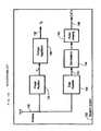
- FIGS. 12 a and 12 b of the accompanying drawingsTwo types of such circuits are shown in FIGS. 12 a and 12 b of the accompanying drawings.
- FIG. 13 of the accompanying drawingsshows examples of a response with high Q 390 and low Q 392 .
- Parallel resonance in a circuit with capacitor 46 of capacitance C, inductor 48 of inductance L, and resistor 50 of resistance Roccurs at the frequency when the reactance due to the inductor is equal and opposite to the reactance due to the capacitor. Parallel resonance results in a maximum voltage across the resistor. The value R of the resistor 50 dictates the value of this voltage. Power transfer at resonance is more efficient as the voltages or currents at resonance are maximized as illustrated in FIG. 14 of the accompanying drawings, which plots the variation of the coupling magnetic field 65 with frequency 64 . At the resonance frequency 60 , the coupling magnetic field 65 is maximum and therefore the power transfer will be maximum at this frequency.
- Wireless transmission of data aloneis well known. The same can be said of wireless power transfer alone.
- Transferring datarequires the data signal to somehow “piggyback” or be carried on the power signal.
- An example of such a techniqueis using the carrier signal to transfer the power and then using Amplitude Shift Keying modulation to couple the data to this carrier as illustrated in FIG. 15 of the accompanying drawings.
- the amplitude of the power carrying signal 74is modified by the data carrying signal 76 .
- the receiver for this scenariois different from the generic receiver illustrated in FIG. 8 as it now has to extract both the power and data from the transmitted signal.
- FIG. 8the generic receiver illustrated in FIG. 8 as it now has to extract both the power and data from the transmitted signal.
- the transmitted signalis coupled to the receiver system 222 via a receive antenna 130 .
- Thisis then followed by two rectifiers (power rectifier 134 and data rectifier 140 ) to extract the power and data signals.
- the output of the power rectifieris an unregulated voltage which is regulated by voltage regulators 136 to provide the required voltage level, V R 138 .
- the output 141 of the data rectifier 140is connected to a demodulator 144 which produces an analogue version of the data signal. This is then passed through a pulse shaping stage 145 to produce a digital signal 146 which is the same as the transmitted data signal.
- x trans( A+x data )
- x cA cos(2 ⁇ f c t )+cos [2 ⁇ t ( f c ⁇ f data )]+cos [2 ⁇ t ( f c +f data )]
- f cis the frequency of the power carrying signal
- f datais the frequency of the data carrying signal
- FIG. 17 of the accompanying drawingsshows the components of the transmitted signal in the frequency domain.
- the frequency components (fc ⁇ fdata 68 ) and (fc+fdata 62 )are termed the sidebands of the transmitted signal. If the data carrying signal 76 has bandwidth, BW, the total bandwidth required to transmit both the sidebands is 2 ⁇ BW 72 .
- FIG. 18 of the accompanying drawingsshows the power carrying signal 60 , the two sidebands 68 , 62 and the system transfer function curve 67 .
- the two sidebandsshould lie within the envelope of the transfer function curve 67 . If the sidebands lie outside the resonance curve 67 , such as at 61 and 63 , data recovery will be impossible. The implication is that it is more difficult to recover both power and data if the data signal has high bandwidth.
- Qquality factor
- the systemuses a form of Frequency Shift Keying (FSK) by transmitting data bit ‘ 0 ’ at one frequency and data bit ‘ 1 ’ at another frequency.
- FSKFrequency Shift Keying
- a major drawback of this methodis that the frequency at which the data bits ‘ 1 ’ and ‘ 0 ’ are transmitted should be highly stable. This is because the high Q of each peak in the transfer function of FIG. 20 results in a locally narrow band system and any deviation of the signal components from these frequencies will completely corrupt the transmitted signal.
- fdata 69 and fc 60should therefore lie exactly at the centre of the respective peaks of the transfer function. This is very difficult if the Q is made very high to allow sufficient power transfer.
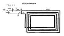
- FIG. 19Another drawback of the system is that only one element of the antenna transmits the signal.
- thiscorresponds to Lp 120 .
- the other inductor Ls, 116does not transmit at all and just functions as a transfer function shaper.
- the amount of power transfer the system can handleis related to the total inductance of the system, this will mean that the amount of power is limited to the amount that the single inductor Lp 120 can transmit.
- the actual implementation of this systemis shown in FIG. 21 of the accompanying drawings where Ls 116 only has the function of shaping the signal and Lp 120 is the only transmitting element. This arrangement would suffice for low power systems. However, for high power system requirements such as powering the backlight of an LC display, a single transmitting element would not supply sufficient power.
- a wireless interfacecomprising a receiving section and a transmitting section arranged to supply signals and power exclusively wirelessly to the receiving section, the transmitting section comprising a transmitter arranged to modulate a carrier with the signals and connected to a transmit antenna comprising a parallel resonant circuit including a first inductor and a series resonant circuit including a second inductor, the receiving section comprising a receive antenna comprising at least one third inductor arranged to be inductively coupled to the first and second inductors.
- the interfacemay comprise a display.
- the receiving sectionmay include an image display device.
- the devicemay be a liquid crystal device.
- the receiving sectionmay include a display backlight.
- the interfacemay comprise a radio frequency identification system.
- the first and second inductorsmay be arranged to be substantially permanently inductively coupled to the at least one third inductor.
- the first and second inductorsmay be arranged to be temporarily inductively coupled to the at least one third inductor.
- the carriermay be a radio frequency carrier.
- the parallel resonant circuit and the series resonant circuitmay be connected in series.
- the first and second inductorsmay be planar inductors.
- the first and second inductorsmay be coplanar.
- One of the first and second inductorsmay be disposed inside the other of the first and second inductors and coaxial therewith.
- the at least one third inductormay be arranged to be coaxial with the first and second inductors.
- the at least one third inductormay be a planar inductor.
- the parallel and series resonant circuitsmay be tuned to different frequencies.
- the parallel and series resonant circuitsmay be tuned substantially to respective sideband frequencies of the modulated carrier.
- the parallel and series resonant circuitsmay have resonant frequencies and Q's such that the carrier and the sidebands of the modulated carrier are within the half power bandwidth of the transmit antenna.
- the receive antennamay comprise a further resonant circuit including the at least one third inductor.
- the further resonant circuitmay be a parallel resonant circuit.
- the further resonant circuitmay be tuned to a frequency between the sidebands of the modulated carrier.
- the further resonant circuitmay be tuned to the geometric mean of the sideband frequencies.
- the further resonant circuitmay have a resonant frequency and a Q such that the carrier and the sidebands of the modulated carrier are within the half power bandwidth of the receive antenna.
- the transmit and receive antennaemay be arranged such that the carrier and sidebands of the modulated carrier are within the half power bandwidth of the inductive coupling.
- the transmittermay be arranged to perform one of amplitude modulation, frequency modulation and phase modulation.
- the receiving sectionmay comprise a demodulator for demodulating signals received by the receive antenna.
- the receiving sectionmay comprise a power supply arrangement arranged to power the whole of the receiving section exclusively from power received by the receive antenna.
- a transmitting section for a wireless interfacefor supplying signals and power exclusively wirelessly to a receiving section of the interface, comprising a transmitter arranged to modulate a carrier with the signals and connected to a transmit antenna comprising a parallel resonant circuit including a first inductor and a series resonant circuit including a second inductor.
- a receiving section for a wireless interfacefor receiving signals and power exclusively wirelessly from a transmitting section of the interface, comprising a receive antenna comprising at least one third inductor arranged to be inductively coupled to first and second inductors of a transmit antenna of the transmitting section.
- FIG. 1is a block schematic diagram of a generic known type of liquid crystal display
- FIG. 2is a block schematic diagram of a known type of integrated display system
- FIG. 3is a block schematic diagram of a generic known type of wireless system
- FIG. 4is a block schematic diagram of a known type of wireless transmitter of a system of the type shown in FIG. 3 ;
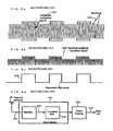
- FIG. 5 ais a timing diagram illustrating Manchester encoding and FIG. 5 b is a diagram illustrating the use of an XOR gate to provide such encoding;
- FIGS. 6 a to 6 ecomprise waveform diagrams illustrating examples of modulation schemes for use in wireless systems
- FIGS. 7 a to 7 care block schematic diagrams illustrating modulators for implementing the modulation schemes illustrated in FIGS. 6 c to 6 e;
- FIG. 8 dis a block schematic diagram of a known type of receiver system and FIGS. 8 a to 8 c are diagrams illustrating waveforms occurring in the receiver system;
- FIG. 9is a circuit diagram illustrating a known type of pulse shaping circuit
- FIG. 10illustrates a known type of power transfer arrangement using magnetic coupling
- FIG. 11is a circuit diagram illustrating a power rectifier for use with the arrangement shown in FIG. 10 ;
- FIGS. 12 a and 12 billustrate examples of known series and parallel resonant circuits
- FIG. 13is a graph of magnetic coupling field against frequency for parallel resonant circuits having different Q's
- FIG. 14is a graph of coupling magnetic field against frequency for a parallel resonant circuit of typical Q
- FIG. 15comprise waveform diagrams illustrating data and power transfer using amplitude shift keying modulation
- FIG. 16illustrates a known type of receiver for extracting power and data
- FIG. 17is a graph illustrating the frequency spectrum of a typical amplitude modulated signal
- FIG. 18is a graph of coupling magnetic field against frequency illustrating bandwidth requirements for transmitting both power and data
- FIG. 19is a circuit diagram illustrating a known type of circuit combining parallel and series resonant circuits
- FIG. 20is a graph of coupling magnetic field against frequency illustrating a transmitter resonant curve
- FIG. 21illustrates diagrammatically a known type of transmit antenna using the circuit of FIG. 19 ;
- FIG. 22is a block schematic diagram of a known type of partially wireless display system
- FIG. 23is a block schematic diagram illustrating a wireless interface for a display constituting an embodiment of the invention.
- FIG. 24is a diagram illustrating a transmit antenna of the interface of FIG. 23 ;
- FIG. 25is a graph of coupling magnetic field against frequency illustrating the performance of the antenna of FIG. 24 ;
- FIG. 26is a diagram illustrating a receive antenna of the interface of FIG. 23 ;
- FIG. 27is a graph of coupling magnetic field against frequency illustrating the coupling performance of the interface of FIG. 23 .
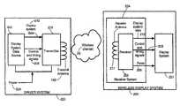
- FIG. 23shows a complete wireless system comprising a driver system 200 constituting a transmitting section and a wireless display system 220 constituting a receiving section.
- the driver system 200comprises a data source 202 to supply the display system data 212 and the control and timing signals 208 . These signals are then connected to the transmitter system 210 which is then connected to a transmit antenna 166 .
- the driver system 200is supplied with power 204 externally to power all the circuitry. After the signal is launched from the transmit antenna 210 , it traverses the wireless channel 26 to couple to the wireless display system 220 .
- the wireless display systemcomprises the receive system 224 which is connected to the display system 257 .
- a receive antenna 211which captures the transmitted signal is connected to a receiver 255 .
- the receiverextracts the display system data 212 , control and timing signals 208 and power 256 from the transmitted signal. These signals are then connected to the display system 257 .
- the wireless display systemis a self-contained system and does not require any external connections. All the data signals 212 , control and timing signals 208 and the power are supplied via the wireless interface completely eliminating the need for a physical connector to the display system for the transmitted signal.
- the display system data source 202 , transmitter system 210 , receiver 255 and display system 257may, for example, be implemented as described hereinbefore and illustrated in FIGS. 2 , 4 , 16 .
- FIG. 24shows an implementation of the transmit antenna 166 which takes the signal to be transmitted (RF IN 124 ) and launches it across the wireless interface.
- the antenna 166comprises a parallel resonant circuit including a first inductor in the form of a parallel coil 120 and a series resonant circuit including a second inductor in the form of a series coil 116 .
- the parallel capacitor 118is used to tune the parallel resonance circuit while capacitor 122 is used to tune the series resonance circuit.
- the tuning of the transmit antenna 166 in FIG. 24is dependent on the modulation scheme used as well as the signal data rate.
- Amplitude Shift Keying (ASK), Frequency Shift Keying (FSK), Phase Shift Keying (PSK) or, indeed, any higher order modulation schememay be used.
- ASICis used as an example.
- a suitable data rate for a mobile displaymay be 6.75 Mb/s. This corresponds to a wave of maximum frequency 3.375 MHz, assuming that non-return to zero (NRZ) data encoding is used.
- the carrier frequencymust be suitably higher than the data rate to reduce the complexity of the demodulation.
- a suitable value of the carrier frequencywould be 8 ⁇ or more the value of the data rate. In this case, 27 MHz is a reasonable choice for the carrier frequency.
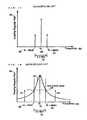
- FIG. 25shows the variation of the coupling magnetic field 65 of the transmit antenna with frequency 64 .
- the responsehas two peaks at the lower sideband (Fc ⁇ Fdata 68 ) and at the upper sideband (Fc ⁇ Fdata 62 ), where Fc is the frequency of the power carrying signal and Fdata is the frequency of the data carrying signal.
- Fcthe frequency of the power carrying signal
- Fdatathe frequency of the data carrying signal.
- the antenna resonance peaksare tuned to these values.
- the series resonanceis tuned to 23.625 MHz while the parallel resonance is tuned to 30.375 MHz.
- the Qs of two resonancesare chosen to be sufficiently high so that the overlap at 27 MHz 400 (in FIG. 25 ) has sufficient power to transmit the carrier.
- a suitable value for the Q for both resonancesis 3 or higher.
- FIG. 26shows an implementation of the receive antenna 211 which is based on a parallel resonance circuit.
- the antenna 211comprises a third inductor in the form of an inductive coil 111 and the tuning capacitor 46 and is designed to resonate at a frequency which is a geometric mean of the two sideband frequencies, i.e., ((Fc+Fdata) (Fc ⁇ Fdata)) 1/2 , which is approximately 27 MHz.
- a suitable Q for the receiver antennais 3 or higher.
- the output signal (RF OUT 112 )connects the signal to the rest of the receiver system.
- the third inductor 111is temporarily or permanently inductively coupled to the first and second inductors 120 , 116 .
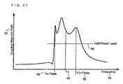
- FIG. 27shows the combined response of the transmit antenna 166 and receive antenna 211 . It plots the variation of the coupling magnetic field 65 with frequency 64 .
- the responseis broadband with a high Q covering the range between the lower sideband (Fc ⁇ Fdata 68 ) and the upper sideband (Fc+Fdata 62 ) of the data carrying signal.
- the half-power level 66is such that the lower sideband 68 and upper sideband 62 lie inside the response curve. This leads to the antenna response having a very high ‘Q’ to aid the transmission of power but also a very broadband response to ensure the transmission of high speed data substantially without any distortion.
Landscapes
- Engineering & Computer Science (AREA)
- Power Engineering (AREA)
- Computer Networks & Wireless Communication (AREA)
- Physics & Mathematics (AREA)
- Life Sciences & Earth Sciences (AREA)
- General Life Sciences & Earth Sciences (AREA)
- General Physics & Mathematics (AREA)
- Geophysics (AREA)
- Near-Field Transmission Systems (AREA)
- Transmitters (AREA)
- Circuits Of Receivers In General (AREA)
- Details Of Aerials (AREA)
Abstract
Description
xc=cos(2πfct),
xdata=cos(2πfdatat),
xtrans=(A+xdata)xc=Acos(2πfct)+cos [2πt(fc−fdata)]+cos [2πt(fc+fdata)]
Q=fc/(2×BW)
Fc−Fdata=23.625
Fc+Fdata=30.375
Claims (28)
Applications Claiming Priority (3)
| Application Number | Priority Date | Filing Date | Title |
|---|---|---|---|
| GB0702842.6 | 2007-02-14 | ||
| GB0702842AGB2446622A (en) | 2007-02-14 | 2007-02-14 | Wireless interface |
| PCT/JP2008/051901WO2008099722A1 (en) | 2007-02-14 | 2008-01-30 | Wireless interface |
Publications (2)
| Publication Number | Publication Date |
|---|---|
| US20100068998A1 US20100068998A1 (en) | 2010-03-18 |
| US8244177B2true US8244177B2 (en) | 2012-08-14 |
Family
ID=37908605
Family Applications (1)
| Application Number | Title | Priority Date | Filing Date |
|---|---|---|---|
| US12/449,510Expired - Fee RelatedUS8244177B2 (en) | 2007-02-14 | 2008-01-30 | Wireless interface |
Country Status (8)
| Country | Link |
|---|---|
| US (1) | US8244177B2 (en) |
| EP (1) | EP2127028A1 (en) |
| JP (1) | JP5015262B2 (en) |
| CN (1) | CN101611518A (en) |
| BR (1) | BRPI0807959A2 (en) |
| GB (1) | GB2446622A (en) |
| RU (1) | RU2415500C1 (en) |
| WO (1) | WO2008099722A1 (en) |
Cited By (11)
| Publication number | Priority date | Publication date | Assignee | Title |
|---|---|---|---|---|
| US9852691B2 (en)* | 2015-01-19 | 2017-12-26 | Samsung Display Co., Ltd. | Display device, system having the same, and pixel |
| US10128678B2 (en) | 2011-02-04 | 2018-11-13 | Qnovo Inc. | Method and circuitry to adaptively charge a battery/cell |
| US10389156B2 (en) | 2010-05-21 | 2019-08-20 | Qnovo Inc. | Method and circuitry to adaptively charge a battery/cell |
| US10417143B2 (en)* | 2015-10-08 | 2019-09-17 | Esker Technologies, LLC | Apparatus and method for sending power over synchronous serial communication wiring |
| US10447055B1 (en) | 2013-04-19 | 2019-10-15 | Qnovo Inc. | Method and circuitry to adaptively charge a battery/cell using a charge-time parameter |
| US10560154B2 (en) | 2016-07-11 | 2020-02-11 | Esker Technologies, LLC | Power line signal coupler |
| US10574079B1 (en)* | 2014-06-20 | 2020-02-25 | Qnovo Inc. | Wireless charging techniques and circuitry for a battery |
| US11397215B2 (en) | 2010-05-21 | 2022-07-26 | Qnovo Inc. | Battery adaptive charging using battery physical phenomena |
| US11397216B2 (en) | 2010-05-21 | 2022-07-26 | Qnovo Inc. | Battery adaptive charging using a battery model |
| US11791647B2 (en) | 2010-05-21 | 2023-10-17 | Qnovo Inc. | Method and circuitry to adaptively charge a battery/cell |
| US12081057B2 (en) | 2010-05-21 | 2024-09-03 | Qnovo Inc. | Method and circuitry to adaptively charge a battery/cell |
Families Citing this family (35)
| Publication number | Priority date | Publication date | Assignee | Title |
|---|---|---|---|---|
| US9130602B2 (en)* | 2006-01-18 | 2015-09-08 | Qualcomm Incorporated | Method and apparatus for delivering energy to an electrical or electronic device via a wireless link |
| US8447234B2 (en)* | 2006-01-18 | 2013-05-21 | Qualcomm Incorporated | Method and system for powering an electronic device via a wireless link |
| GB2446622A (en) | 2007-02-14 | 2008-08-20 | Sharp Kk | Wireless interface |
| US8482157B2 (en)* | 2007-03-02 | 2013-07-09 | Qualcomm Incorporated | Increasing the Q factor of a resonator |
| US9774086B2 (en)* | 2007-03-02 | 2017-09-26 | Qualcomm Incorporated | Wireless power apparatus and methods |
| US8378523B2 (en)* | 2007-03-02 | 2013-02-19 | Qualcomm Incorporated | Transmitters and receivers for wireless energy transfer |
| US9124120B2 (en)* | 2007-06-11 | 2015-09-01 | Qualcomm Incorporated | Wireless power system and proximity effects |
| WO2009036405A1 (en) | 2007-09-13 | 2009-03-19 | Nigelpower, Llc | Maximizing power yield from wireless power magnetic resonators |
| JP5362733B2 (en)* | 2007-10-11 | 2013-12-11 | クゥアルコム・インコーポレイテッド | Wireless power transfer using a magneto-mechanical system |
| US8629576B2 (en)* | 2008-03-28 | 2014-01-14 | Qualcomm Incorporated | Tuning and gain control in electro-magnetic power systems |
| US20090273242A1 (en)* | 2008-05-05 | 2009-11-05 | Nigelpower, Llc | Wireless Delivery of power to a Fixed-Geometry power part |
| US20090299918A1 (en)* | 2008-05-28 | 2009-12-03 | Nigelpower, Llc | Wireless delivery of power to a mobile powered device |
| US8132037B2 (en)* | 2008-06-06 | 2012-03-06 | Roche Diagnostics International Ag | Apparatus and method for processing wirelessly communicated data and clock information within an electronic device |
| US8111042B2 (en)* | 2008-08-05 | 2012-02-07 | Broadcom Corporation | Integrated wireless resonant power charging and communication channel |
| JP4645698B2 (en)* | 2008-08-19 | 2011-03-09 | ソニー株式会社 | Wireless communication device and power receiving device |
| KR101718715B1 (en) | 2010-04-28 | 2017-03-22 | 삼성전자주식회사 | Method and Apparatus of Controlling of Resonance Bandwidth in Wireless Power Transform System |
| CN103180955B (en)* | 2010-08-23 | 2018-10-16 | L·皮尔·德罗什蒙 | Power Field Effect Transistor with Resonant Transistor Gate |
| US8995907B2 (en)* | 2011-06-24 | 2015-03-31 | Baker Hughes Incorporated | Data communication system |
| RU2475644C1 (en)* | 2011-07-15 | 2013-02-20 | Государственное образовательное учреждение высшего профессионального образования "Омский государственный университет им. Ф.М. Достоевского" | Method of reception and transmission of data from well bottom to surface by electromagnetic communication channel by rock using superconducting quantum interference device |
| US9179492B2 (en) | 2011-10-26 | 2015-11-03 | Texas Instruments Deutschland Gmbh | Electronic device, method and system for half duplex data transmission |
| US8862104B2 (en)* | 2012-06-29 | 2014-10-14 | Intel Corporation | System and method for gesture-based management |
| US9859744B2 (en) | 2012-08-03 | 2018-01-02 | Mediatek Singapore Pte. Ltd. | Dual-mode wireless power receiver |
| US9912197B2 (en) | 2012-08-03 | 2018-03-06 | Mediatek Singapore Pte. Ltd. | Dual-mode wireless power receiver |
| US10658869B2 (en) | 2012-08-03 | 2020-05-19 | Mediatek Inc. | Multi-mode, multi-standard wireless power transmitter coil assembly |
| WO2014158504A1 (en)* | 2013-03-14 | 2014-10-02 | Mediatek Singapore Pte. Ltd. | Dual-mode wireless power receiver |
| US9601267B2 (en) | 2013-07-03 | 2017-03-21 | Qualcomm Incorporated | Wireless power transmitter with a plurality of magnetic oscillators |
| US10135305B2 (en) | 2014-06-10 | 2018-11-20 | Mediatek Singapore Pte. Ltd. | Multi-mode wireless power transmitter |
| US9787353B2 (en)* | 2015-07-13 | 2017-10-10 | Qorvo Us, Inc. | Radio frequency (RF) front-end without signal switches |
| US10461812B2 (en) | 2016-04-01 | 2019-10-29 | Nan Jing Qiwei Technology Limited | Near-field communication (NFC) tags optimized for high performance NFC and wireless power reception with small antennas |
| US10153809B2 (en)* | 2016-04-01 | 2018-12-11 | Fusens Technology Limited | Near-field communication (NFC) reader optimized for high performance NFC and wireless power transfer with small antennas |
| US10666325B2 (en) | 2016-04-01 | 2020-05-26 | Nan Jing Qiwei Technology Limited | Near-field communication (NFC) system and method for high performance NFC and wireless power transfer with small antennas |
| TW201817080A (en)* | 2016-10-24 | 2018-05-01 | 財團法人金屬工業硏究發展中心 | Microstrip antenna structure and microwave imaging system using the same |
| JP7414405B2 (en)* | 2019-05-23 | 2024-01-16 | キヤノン株式会社 | Control system and control method |
| EP4084314A4 (en)* | 2020-01-07 | 2022-12-28 | Guangdong Oppo Mobile Telecommunications Corp., Ltd. | ADAPTER AND ORDERING METHOD |
| EP3934057B1 (en)* | 2020-04-29 | 2024-03-20 | Huawei Digital Power Technologies Co., Ltd. | Long-distance wireless charging transmitting end, receiving end, and system |
Citations (32)
| Publication number | Priority date | Publication date | Assignee | Title |
|---|---|---|---|---|
| JPS6473918A (en) | 1987-09-16 | 1989-03-20 | Nec Corp | Antenna for small sized radio equipment |
| JPH0746515A (en) | 1993-07-28 | 1995-02-14 | Sharp Corp | Information input / output device |
| JPH09298500A (en) | 1996-05-09 | 1997-11-18 | Citizen Watch Co Ltd | Communication circuit for contactless memory card |
| JPH09298485A (en) | 1996-04-30 | 1997-11-18 | Yamatake Honeywell Co Ltd | Non-contact data transmission / reception method and device |
| GB2331638A (en) | 1997-11-19 | 1999-05-26 | Ackermann Ltd | Inductive power transfer to mobile electrical equipment |
| JPH11332135A (en) | 1998-03-03 | 1999-11-30 | Seiko Epson Corp | Electronics |
| JPH11353438A (en) | 1998-06-04 | 1999-12-24 | Canon Inc | Card device |
| JP2000059261A (en) | 1998-08-06 | 2000-02-25 | Yamatake Corp | Non-contact data transmission / reception device |
| JP2000113144A (en) | 1998-10-06 | 2000-04-21 | Hitachi Chem Co Ltd | Non-contact type ic card |
| US6088741A (en) | 1996-05-09 | 2000-07-11 | Citizen Watch Co., Ltd. | Storage medium system which uses a contactless memory card |
| JP2002032728A (en) | 2000-07-18 | 2002-01-31 | Toshiba Corp | Wireless card system |
| US20020152606A1 (en) | 2001-04-19 | 2002-10-24 | Chi-Fang Huang | Printed-on-display antenna of wireless mobile personal terminal |
| US6533178B1 (en) | 1998-05-15 | 2003-03-18 | Infineon Technologies Ag | Device for contactless transmission of data |
| US6575374B1 (en) | 1999-10-28 | 2003-06-10 | Ask S.A. | Coupling antenna with high inductance |
| JP2004102840A (en) | 2002-09-11 | 2004-04-02 | Fuji Xerox Co Ltd | Electronic media |
| EP1538558A2 (en) | 2003-12-03 | 2005-06-08 | Hitachi, Ltd. | RFID with a resonant circuit |
| EP1547719A2 (en) | 2003-12-26 | 2005-06-29 | Semiconductor Energy Laboratory Co., Ltd. | Laser irradiation apparatus, laser irradiation method, and method for manufacturing crystalline semiconductor film |
| US20060083955A1 (en) | 2004-10-19 | 2006-04-20 | Akihiko Kanouda | Mobile type information terminal and self diagnosis method and operation method thereof |
| US7071629B2 (en) | 2003-03-31 | 2006-07-04 | Sony Corporation | Image display device incorporating driver circuits on active substrate and other methods to reduce interconnects |
| CA2543655A1 (en) | 2005-05-13 | 2006-07-19 | Research In Motion Limited | Communications system including units with lcd optical transmitters/receivers and related methods |
| US7183987B2 (en)* | 2002-09-27 | 2007-02-27 | Sony Corporation | Antenna apparatus, and communications apparatus using same |
| GB2431821A (en) | 2005-10-27 | 2007-05-02 | Hewlett Packard Development Co | Inductively powered devices |
| US20070158804A1 (en) | 2006-01-10 | 2007-07-12 | Semiconductor Energy Laboratory Co., Ltd. | Semiconductor device, manufacturing method of semiconductor device, and RFID tag |
| US20070197049A1 (en) | 2006-02-17 | 2007-08-23 | Semiconductor Energy Laboratory Co., Ltd. | Method for manufacturing semiconductor device |
| US20070195834A1 (en) | 2006-02-21 | 2007-08-23 | Semiconductor Energy Laboratory Co., Ltd. | Laser irradiation apparatus, method of laser irradiation, and method for manufacturing semiconductor device |
| US20080067874A1 (en)* | 2006-09-14 | 2008-03-20 | Ryan Tseng | Method and apparatus for wireless power transmission |
| US20080153416A1 (en)* | 2006-09-11 | 2008-06-26 | Takanori Washiro | Communication System and Communication Apparatus |
| WO2008099722A1 (en) | 2007-02-14 | 2008-08-21 | Sharp Kabushiki Kaisha | Wireless interface |
| US20080227478A1 (en)* | 2007-03-15 | 2008-09-18 | Greene Charles E | Multiple frequency transmitter, receiver, and systems thereof |
| US7764928B2 (en)* | 2006-01-19 | 2010-07-27 | Murata Manufacturing Co., Ltd. | Wireless IC device and component for wireless IC device |
| US20100237707A1 (en)* | 2005-07-12 | 2010-09-23 | Aristeidis Karalis | Increasing the q factor of a resonator |
| US20110043328A1 (en)* | 2007-01-29 | 2011-02-24 | Fred Bassali | Advanced Vehicular Universal Transmitter Using Time Domain With Vehicle LocationLoggin System |
Family Cites Families (1)
| Publication number | Priority date | Publication date | Assignee | Title |
|---|---|---|---|---|
| JP4203460B2 (en)* | 2004-10-19 | 2009-01-07 | 株式会社日立超エル・エス・アイ・システムズ | Portable information terminal and method of operating portable information terminal |
- 2007
- 2007-02-14GBGB0702842Apatent/GB2446622A/ennot_activeWithdrawn
- 2008
- 2008-01-30RURU2009132094/07Apatent/RU2415500C1/ennot_activeIP Right Cessation
- 2008-01-30CNCNA200880004614XApatent/CN101611518A/enactivePending
- 2008-01-30WOPCT/JP2008/051901patent/WO2008099722A1/enactiveApplication Filing
- 2008-01-30JPJP2009537949Apatent/JP5015262B2/ennot_activeExpired - Fee Related
- 2008-01-30BRBRPI0807959-5A2Apatent/BRPI0807959A2/ennot_activeIP Right Cessation
- 2008-01-30USUS12/449,510patent/US8244177B2/ennot_activeExpired - Fee Related
- 2008-01-30EPEP08704474Apatent/EP2127028A1/ennot_activeWithdrawn
Patent Citations (35)
| Publication number | Priority date | Publication date | Assignee | Title |
|---|---|---|---|---|
| JPS6473918A (en) | 1987-09-16 | 1989-03-20 | Nec Corp | Antenna for small sized radio equipment |
| JPH0746515A (en) | 1993-07-28 | 1995-02-14 | Sharp Corp | Information input / output device |
| JPH09298485A (en) | 1996-04-30 | 1997-11-18 | Yamatake Honeywell Co Ltd | Non-contact data transmission / reception method and device |
| US6088741A (en) | 1996-05-09 | 2000-07-11 | Citizen Watch Co., Ltd. | Storage medium system which uses a contactless memory card |
| JPH09298500A (en) | 1996-05-09 | 1997-11-18 | Citizen Watch Co Ltd | Communication circuit for contactless memory card |
| GB2331638A (en) | 1997-11-19 | 1999-05-26 | Ackermann Ltd | Inductive power transfer to mobile electrical equipment |
| JPH11332135A (en) | 1998-03-03 | 1999-11-30 | Seiko Epson Corp | Electronics |
| US6533178B1 (en) | 1998-05-15 | 2003-03-18 | Infineon Technologies Ag | Device for contactless transmission of data |
| RU2213370C2 (en) | 1998-05-15 | 2003-09-27 | Инфинеон Текнолоджиз Аг | Contactless data transmission device |
| JPH11353438A (en) | 1998-06-04 | 1999-12-24 | Canon Inc | Card device |
| JP2000059261A (en) | 1998-08-06 | 2000-02-25 | Yamatake Corp | Non-contact data transmission / reception device |
| JP2000113144A (en) | 1998-10-06 | 2000-04-21 | Hitachi Chem Co Ltd | Non-contact type ic card |
| US6575374B1 (en) | 1999-10-28 | 2003-06-10 | Ask S.A. | Coupling antenna with high inductance |
| JP2002032728A (en) | 2000-07-18 | 2002-01-31 | Toshiba Corp | Wireless card system |
| US20020152606A1 (en) | 2001-04-19 | 2002-10-24 | Chi-Fang Huang | Printed-on-display antenna of wireless mobile personal terminal |
| JP2004102840A (en) | 2002-09-11 | 2004-04-02 | Fuji Xerox Co Ltd | Electronic media |
| US7183987B2 (en)* | 2002-09-27 | 2007-02-27 | Sony Corporation | Antenna apparatus, and communications apparatus using same |
| US7071629B2 (en) | 2003-03-31 | 2006-07-04 | Sony Corporation | Image display device incorporating driver circuits on active substrate and other methods to reduce interconnects |
| EP1538558A2 (en) | 2003-12-03 | 2005-06-08 | Hitachi, Ltd. | RFID with a resonant circuit |
| EP1547719A2 (en) | 2003-12-26 | 2005-06-29 | Semiconductor Energy Laboratory Co., Ltd. | Laser irradiation apparatus, laser irradiation method, and method for manufacturing crystalline semiconductor film |
| US20060083955A1 (en) | 2004-10-19 | 2006-04-20 | Akihiko Kanouda | Mobile type information terminal and self diagnosis method and operation method thereof |
| CA2543655A1 (en) | 2005-05-13 | 2006-07-19 | Research In Motion Limited | Communications system including units with lcd optical transmitters/receivers and related methods |
| US20100237707A1 (en)* | 2005-07-12 | 2010-09-23 | Aristeidis Karalis | Increasing the q factor of a resonator |
| US20110074347A1 (en)* | 2005-07-12 | 2011-03-31 | Aristeidis Karalis | Wireless energy transfer |
| US20100253152A1 (en)* | 2005-07-12 | 2010-10-07 | Aristeidis Karalis | Long range low frequency resonator |
| GB2431821A (en) | 2005-10-27 | 2007-05-02 | Hewlett Packard Development Co | Inductively powered devices |
| US20070158804A1 (en) | 2006-01-10 | 2007-07-12 | Semiconductor Energy Laboratory Co., Ltd. | Semiconductor device, manufacturing method of semiconductor device, and RFID tag |
| US7764928B2 (en)* | 2006-01-19 | 2010-07-27 | Murata Manufacturing Co., Ltd. | Wireless IC device and component for wireless IC device |
| US20070197049A1 (en) | 2006-02-17 | 2007-08-23 | Semiconductor Energy Laboratory Co., Ltd. | Method for manufacturing semiconductor device |
| US20070195834A1 (en) | 2006-02-21 | 2007-08-23 | Semiconductor Energy Laboratory Co., Ltd. | Laser irradiation apparatus, method of laser irradiation, and method for manufacturing semiconductor device |
| US20080153416A1 (en)* | 2006-09-11 | 2008-06-26 | Takanori Washiro | Communication System and Communication Apparatus |
| US20080067874A1 (en)* | 2006-09-14 | 2008-03-20 | Ryan Tseng | Method and apparatus for wireless power transmission |
| US20110043328A1 (en)* | 2007-01-29 | 2011-02-24 | Fred Bassali | Advanced Vehicular Universal Transmitter Using Time Domain With Vehicle LocationLoggin System |
| WO2008099722A1 (en) | 2007-02-14 | 2008-08-21 | Sharp Kabushiki Kaisha | Wireless interface |
| US20080227478A1 (en)* | 2007-03-15 | 2008-09-18 | Greene Charles E | Multiple frequency transmitter, receiver, and systems thereof |
Non-Patent Citations (12)
| Title |
|---|
| Behzad Razavi, "Design of Analog CMOS Integrated Circuits", Mc-Graw-Hill 2001. |
| E. Zambyo et al., "A Fully Monolithic Wireless Display System" ECS Transactions vol. 16, Issue 9, p. 309-312, Oct. 12, 2008. |
| E. Zambyo et al., "A Fully Monolithic Wireless Display System" Late Technical news submission to the International Display Workshop (IDW07) 2007. |
| E. Zambyo et al., "A Fully Monolithic Wireless Display System" The Fifteenth International Workshop on Active-Matrix Flat Pane Displays and Devices, Jul. 2-4, 2008. |
| E. Zyambo et al. "A Fully Monolithic Wireless Display System." ECS Trans., 16, 3 (2008) DOI:10.1149/1.2980525. |
| E. Zyambo et al. "A Fully Monolithic Wireless Display System." Proceedings of the 14th International Display Workshops, 2007. |
| E. Zyambo et al. "A Fully Monolithic Wireless Display System." The 15th International Workshop on Active-Matrix Flatpanel Displays and Devices, (AM-FPD 08), 2008. |
| English translation of International Search Report issued for International Patent Application No. PCT/JP2008/060037. |
| International Search Report. |
| M. Ghovanloo et al., "A widespread Frequency-Shift Keying Wireless Link for Inductively Powered Biomedical Implants" IEEE Trans. on Circuits and Systems, vol. 51, No. 12, Dec. 2004, pp. 2374-2383. |
| R. Jacob Baker et al., "CMOS, Circuit design, Layout and Simulation" IEEE Press 1998. |
| Search Report dated Jun. 21, 2007 for the UK patent application No. GB0702842.6. |
Cited By (18)
| Publication number | Priority date | Publication date | Assignee | Title |
|---|---|---|---|---|
| US12081057B2 (en) | 2010-05-21 | 2024-09-03 | Qnovo Inc. | Method and circuitry to adaptively charge a battery/cell |
| US12132339B2 (en) | 2010-05-21 | 2024-10-29 | Qnovo Inc. | Battery adaptive charging using a battery model |
| US10389156B2 (en) | 2010-05-21 | 2019-08-20 | Qnovo Inc. | Method and circuitry to adaptively charge a battery/cell |
| US12438386B2 (en) | 2010-05-21 | 2025-10-07 | Qnovo Inc. | Method and circuitry to adaptively charge a battery/cell |
| US12249694B2 (en) | 2010-05-21 | 2025-03-11 | Qnovo Inc. | Battery adaptive charging |
| US12176497B2 (en) | 2010-05-21 | 2024-12-24 | Qnovo Inc. | Battery adaptive charging |
| US12136708B2 (en) | 2010-05-21 | 2024-11-05 | Qnovo Inc. | Battery adaptive charging using battery physical phenomena |
| US11063459B2 (en) | 2010-05-21 | 2021-07-13 | Qnovo Inc. | Method and circuitry to adaptively charge a battery/cell |
| US11397215B2 (en) | 2010-05-21 | 2022-07-26 | Qnovo Inc. | Battery adaptive charging using battery physical phenomena |
| US11728525B2 (en) | 2010-05-21 | 2023-08-15 | Qnovo Inc. | Battery adaptive charging |
| US11397216B2 (en) | 2010-05-21 | 2022-07-26 | Qnovo Inc. | Battery adaptive charging using a battery model |
| US11791647B2 (en) | 2010-05-21 | 2023-10-17 | Qnovo Inc. | Method and circuitry to adaptively charge a battery/cell |
| US10128678B2 (en) | 2011-02-04 | 2018-11-13 | Qnovo Inc. | Method and circuitry to adaptively charge a battery/cell |
| US10447055B1 (en) | 2013-04-19 | 2019-10-15 | Qnovo Inc. | Method and circuitry to adaptively charge a battery/cell using a charge-time parameter |
| US10574079B1 (en)* | 2014-06-20 | 2020-02-25 | Qnovo Inc. | Wireless charging techniques and circuitry for a battery |
| US9852691B2 (en)* | 2015-01-19 | 2017-12-26 | Samsung Display Co., Ltd. | Display device, system having the same, and pixel |
| US10417143B2 (en)* | 2015-10-08 | 2019-09-17 | Esker Technologies, LLC | Apparatus and method for sending power over synchronous serial communication wiring |
| US10560154B2 (en) | 2016-07-11 | 2020-02-11 | Esker Technologies, LLC | Power line signal coupler |
Also Published As
| Publication number | Publication date |
|---|---|
| CN101611518A (en) | 2009-12-23 |
| GB2446622A (en) | 2008-08-20 |
| US20100068998A1 (en) | 2010-03-18 |
| WO2008099722A1 (en) | 2008-08-21 |
| RU2415500C1 (en) | 2011-03-27 |
| JP2010511316A (en) | 2010-04-08 |
| BRPI0807959A2 (en) | 2014-06-10 |
| EP2127028A1 (en) | 2009-12-02 |
| JP5015262B2 (en) | 2012-08-29 |
| GB0702842D0 (en) | 2007-03-28 |
Similar Documents
| Publication | Publication Date | Title |
|---|---|---|
| US8244177B2 (en) | Wireless interface | |
| US20190074726A1 (en) | Wireless power feeding system, wireless power transmitter, and wireless power receiver | |
| CN101861703B (en) | Transceiving circuit for contactless communication | |
| US8629760B2 (en) | Signal conversion device, radio frequency identification (RFID) tag, and method for operating the RFID tag | |
| JP2016517662A (en) | Load modulation of direct power transmission in near field communication devices | |
| US8811542B2 (en) | HDX demodulator | |
| US10419254B2 (en) | Transmission apparatus for a wireless device using delta-sigma modulation | |
| US20090247079A1 (en) | Terminal of radio-frequency transmission/reception by inductive coupling | |
| US8690071B2 (en) | Transponder | |
| US8159291B2 (en) | AM (amplitude modulation) demodulation system for RFID reader device | |
| WO1998058347A1 (en) | Non-contact ic card system and non-contact ic card | |
| US7791409B2 (en) | AM (amplitude modulation) demodulation system for RFID reader device | |
| US7573368B2 (en) | Electromagnetic transponder with no autonomous power supply | |
| CN104335494B (en) | Method and apparatus for generating a dedicated data channel in an inductively coupled RFID system using bandpass modulation | |
| JP2004206383A (en) | Non-contact IC card reading / writing device | |
| CN1192478C (en) | Method for modulating the amplitude of an antenna signal | |
| JP4067638B2 (en) | Data carrier system and interrogator for data carrier system | |
| Cho et al. | An analog front-end IP for 13.56 MHz RFID interrogators | |
| KR20060011241A (en) | AFF circuit of RFID reader and RFID reader using it | |
| CN113902078B (en) | Remote ID identity recognition method and system suitable for being within 1500 meters | |
| CN102567777B (en) | Non-contact IC card parameter determination device and method | |
| JP4528650B2 (en) | Wireless communication device and non-contact IC card reader / writer device | |
| JPWO2004051880A1 (en) | Non-contact non-power IC card system | |
| JP2005528055A (en) | Passive data carrier with signal evaluation means for evaluating self-clocking signal information | |
| JP2004538697A (en) | Contactless smart card interrogation device |
Legal Events
| Date | Code | Title | Description |
|---|---|---|---|
| AS | Assignment | Owner name:SHARP KABUSHIKI KAISHA,JAPAN Free format text:ASSIGNMENT OF ASSIGNORS INTEREST;ASSIGNORS:ZYAMBO, EMMANUEL;LUKAMA, LLOYD;BROWN, CHRISTOPHER JAMES;AND OTHERS;SIGNING DATES FROM 20090703 TO 20090810;REEL/FRAME:023088/0210 Owner name:SHARP KABUSHIKI KAISHA, JAPAN Free format text:ASSIGNMENT OF ASSIGNORS INTEREST;ASSIGNORS:ZYAMBO, EMMANUEL;LUKAMA, LLOYD;BROWN, CHRISTOPHER JAMES;AND OTHERS;SIGNING DATES FROM 20090703 TO 20090810;REEL/FRAME:023088/0210 | |
| ZAAA | Notice of allowance and fees due | Free format text:ORIGINAL CODE: NOA | |
| ZAAB | Notice of allowance mailed | Free format text:ORIGINAL CODE: MN/=. | |
| STCF | Information on status: patent grant | Free format text:PATENTED CASE | |
| FEPP | Fee payment procedure | Free format text:PAYOR NUMBER ASSIGNED (ORIGINAL EVENT CODE: ASPN); ENTITY STATUS OF PATENT OWNER: LARGE ENTITY | |
| FPAY | Fee payment | Year of fee payment:4 | |
| MAFP | Maintenance fee payment | Free format text:PAYMENT OF MAINTENANCE FEE, 8TH YEAR, LARGE ENTITY (ORIGINAL EVENT CODE: M1552); ENTITY STATUS OF PATENT OWNER: LARGE ENTITY Year of fee payment:8 | |
| FEPP | Fee payment procedure | Free format text:MAINTENANCE FEE REMINDER MAILED (ORIGINAL EVENT CODE: REM.); ENTITY STATUS OF PATENT OWNER: LARGE ENTITY | |
| LAPS | Lapse for failure to pay maintenance fees | Free format text:PATENT EXPIRED FOR FAILURE TO PAY MAINTENANCE FEES (ORIGINAL EVENT CODE: EXP.); ENTITY STATUS OF PATENT OWNER: LARGE ENTITY | |
| STCH | Information on status: patent discontinuation | Free format text:PATENT EXPIRED DUE TO NONPAYMENT OF MAINTENANCE FEES UNDER 37 CFR 1.362 | |
| FP | Lapsed due to failure to pay maintenance fee | Effective date:20240814 |