US8243525B1 - Refreshing non-volatile semiconductor memory by reading without rewriting - Google Patents
Refreshing non-volatile semiconductor memory by reading without rewritingDownload PDFInfo
- Publication number
- US8243525B1 US8243525B1US12/571,330US57133009AUS8243525B1US 8243525 B1US8243525 B1US 8243525B1US 57133009 AUS57133009 AUS 57133009AUS 8243525 B1US8243525 B1US 8243525B1
- Authority
- US
- United States
- Prior art keywords
- memory
- read
- memory device
- data
- read command
- Prior art date
- Legal status (The legal status is an assumption and is not a legal conclusion. Google has not performed a legal analysis and makes no representation as to the accuracy of the status listed.)
- Expired - Fee Related, expires
Links
- 239000004065semiconductorSubstances0.000titleclaimsabstractdescription25
- 230000015654memoryEffects0.000claimsabstractdescription59
- 238000000034methodMethods0.000claimsdescription11
- 238000010586diagramMethods0.000description9
- 210000004027cellAnatomy0.000description6
- 210000000352storage cellAnatomy0.000description4
- 230000000593degrading effectEffects0.000description2
- 230000014759maintenance of locationEffects0.000description2
- 230000015556catabolic processEffects0.000description1
- 238000004891communicationMethods0.000description1
- 230000007423decreaseEffects0.000description1
- 238000006731degradation reactionMethods0.000description1
- 230000001934delayEffects0.000description1
- 230000007613environmental effectEffects0.000description1
- 239000007787solidSubstances0.000description1
Images


Classifications
- G—PHYSICS
- G11—INFORMATION STORAGE
- G11C—STATIC STORES
- G11C16/00—Erasable programmable read-only memories
- G11C16/02—Erasable programmable read-only memories electrically programmable
- G11C16/06—Auxiliary circuits, e.g. for writing into memory
- G11C16/34—Determination of programming status, e.g. threshold voltage, overprogramming or underprogramming, retention
- G11C16/349—Arrangements for evaluating degradation, retention or wearout, e.g. by counting erase cycles
- G11C16/3495—Circuits or methods to detect or delay wearout of nonvolatile EPROM or EEPROM memory devices, e.g. by counting numbers of erase or reprogram cycles, by using multiple memory areas serially or cyclically
- G—PHYSICS
- G11—INFORMATION STORAGE
- G11C—STATIC STORES
- G11C16/00—Erasable programmable read-only memories
- G11C16/02—Erasable programmable read-only memories electrically programmable
- G11C16/06—Auxiliary circuits, e.g. for writing into memory
- G11C16/34—Determination of programming status, e.g. threshold voltage, overprogramming or underprogramming, retention
- G11C16/3418—Disturbance prevention or evaluation; Refreshing of disturbed memory data
- G11C16/3431—Circuits or methods to detect disturbed nonvolatile memory cells, e.g. which still read as programmed but with threshold less than the program verify threshold or read as erased but with threshold greater than the erase verify threshold, and to reverse the disturbance via a refreshing programming or erasing step
Definitions
- a non-volatile semiconductor memorymay be employed as mass storage for a computer system (e.g., desktop, laptop, portable, etc.) or a consumer device (e.g., music player, cell phone, camera, etc.) or other suitable application.
- the non-volatile semiconductor memorymay comprise one or more memory devices (such as a flash memory) and control circuitry for accessing each memory device. Each memory device is coupled to an I/O bus, as well as a number of interface control lines.
- the control circuitrytransfers the address and command data (and write data for a program operation) over the I/O bus.
- the control circuitrytransfers the address and command data over the I/O bus and then receives the read data over the I/O bus.
- flash memoryis non-volatile (retains data when power is removed), the charge on the floating gate of each storage cell will eventually degrade over time until the retention capability is lost.
- the retention degradationmay be precipitated by environmental conditions (e.g., temperature), as well as interference when accessing adjacent or near adjacent cells.
- environmental conditionse.g., temperature
- interferencee.g., temperature
- the storage cellsare periodically refreshed (by reading and rewriting the data) after a predetermined interval and/or after a number of access operations to adjacent cells.
- rewriting the storage cells during a refresh operationtakes time which degrades overall performance of the memory device, and it consumes power which may be a concern in portable applications.
- a non-volatile semiconductor memorytypically has a limited number of erase/program cycles. If the storage cells must first be erased before being rewritten during a refresh operation, each refresh operation decreases the remaining number of erase/program cycles.
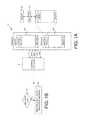
- FIG. 1Ashows a non-volatile semiconductor memory according to an embodiment of the present invention comprising a plurality of memory devices (e.g., flash memories) and control circuitry (e.g., a flash controller).
- memory devicese.g., flash memories
- control circuitrye.g., a flash controller
- FIG. 1Bis a flow diagram executed by the control circuitry according to an embodiment of the present invention wherein when a memory segment of a memory device needs refreshing, data is read from the memory segment without rewriting the data.
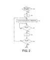
- FIG. 2is a flow diagram according to an embodiment of the present invention wherein each memory device comprises a plurality of blocks, each block comprises a plurality of pages, and the pages of a block are refreshed together to mitigate read disturb.
- FIG. 3Ashows an embodiment of the present invention wherein a PAGE CACHE READ command is issued to the memory device to expedite the refresh operation.
- FIG. 3Bshows an embodiment of the present invention wherein a status is read from a status register in the memory device to determine when a refresh read has been completed.
- FIG. 3Cshows a status register wherein bit 5 indicates whether a refresh read has finished reading data from the memory segment into the data register.
- FIG. 4Ashows an embodiment of the present invention wherein refresh read commands are issued to a plurality of memory devices in an order based on the read time of each memory device.
- FIG. 4Billustrates how the read time is measured for each memory device relative to when the status register indicates a read operation has completed.
- FIG. 5is a flow diagram according to an embodiment of the present invention wherein the read times for each memory device is measured, and then the refresh read commands are issued to the memory devices in an order based on the read times.
- FIG. 6shows a non-volatile semiconductor memory according to an embodiment of the present invention wherein a flash memory comprises the control circuitry and the memory device (e.g., a NAND array).
- a flash memorycomprises the control circuitry and the memory device (e.g., a NAND array).
- FIG. 1Ashows a non-volatile semiconductor memory 2 according to an embodiment of the present invention comprising a first memory device 4 A including a plurality of memory segments, and control circuitry 6 operable to execute the flow diagram of FIG. 1B .
- the control circuitry 6determines whether a memory segment in the first memory device needs refreshing (step 8 ), and when the memory segment needs refreshing, reads data from the memory segment into a data register 12 without rewriting the data (step 10 ).
- the non-volatile semiconductor memory 2may comprise any suitable configuration of control circuitry 6 and memory devices 4 A- 4 B.
- each memory device 4 A- 4 Bcomprises a suitable flash memory (e.g., NAND or NOR flash), and the control circuitry 6 comprises a suitable flash controller.
- the control circuitry 6implements a solid state drive (SSD) by emulating a disk drive accessible by a host system using a standard disk drive communication protocol (e.g., the ATA protocol).
- SSDsolid state drive
- the control circuitry 6may be implemented within the flash memory, that is, the flash memory may implement the refresh algorithm internally rather than implemented by the flash controller.
- each memory devicecomprises a plurality of blocks, wherein each block comprises a plurality of pages.
- the blocksare accessed a page at a time through the data register 12 . That is, write data is stored in the data register 12 and then the control circuitry 6 issues a write command to flush the data in the register 12 to the target page. During a read operation, the data is read from the page into the data register 12 , and then transferred to the control circuitry 6 .
- the memory segment that is refreshedmay comprise a partial page, a single page, multiple pages, an entire block, or multiple blocks.
- the control circuitry 6may implement any suitable refresh algorithm for determining when a memory segment in one of the memory devices needs refreshing. For example, the control circuitry 6 may determine that a memory segment needs refreshing after a predetermined interval, or after a predetermined number of write and/or read operations to proximate memory segments, or a combination of these or other factors. In another embodiment, the control circuitry 6 may execute the refresh algorithm when the non-volatile semiconductor memory 2 is idle (not processing access commands from a host) regardless as to whether the data may be degrading.
- the control circuitry 6When a memory segment needs refreshing, the control circuitry 6 reads the data from the memory segment into the data register 12 without rewriting the data into the same or other memory device. In one embodiment, the control circuitry 6 does not read the data from the data register 12 since there is no use for the data. The data in the data register 12 is simply overwritten during the next access operation (refresh read or normal read/write operation).
- the prior artteaches that a non-volatile semiconductor memory must be rewritten in order to refresh the memory segments, whereas the inventors have discovered that performing a read operation alone will effectuate a refresh operation. Refreshing the memory segments without rewriting the data improves performance, reduces power consumption, and increases endurance since an erase/program cycle is avoided.
- FIG. 2is a flow diagram according to an embodiment of the present invention wherein each memory device comprises a plurality of blocks, and each block comprises a plurality of pages.
- each memory devicecomprises a plurality of blocks, and each block comprises a plurality of pages.
- a page counter iis initialized to zero (step 16 ).
- a commandis issued to read page[i], and when the memory device returns a ready status indicating that the read operation is completed (step 20 ), the page counter i is incremented (step 22 ) and the next page is read (step 18 ). This process is repeated until all of the pages in the block have been read (step 24 ).
- FIG. 1Aillustrates an embodiment of the present invention wherein each memory device (e.g., memory device 4 B) comprises a cache register 26 .
- the control circuitry 6transfers the write data to the cache register 26 .
- the memory devicethen transfers the write data from the cache register 26 to the data register 12 .
- the memory devicesignals the control circuitry 6 that it is ready to receive another write command.
- new write datacan be received from the control circuitry 6 and stored in the cache register 26 while the write data stored in the data register 12 is being programmed into the target page.
- the read datais read from a page into the data register 12 , and then transferred into the cache register 26 . In this manner, a next page can be read into the data register 12 while the previous read data is transferred from the cache register 26 to the control circuitry 6 .
- FIG. 3Aillustrates an embodiment of the present invention wherein the cache mode of the memory device is exploited to increase the performance of a refresh operation.
- a PAGE READ commandis issued to read the first page of memory.
- the PAGE READ commandcomprises the control command 00h followed by the address of the first page of the block, followed by the control command 30h (an “A” cycle in FIG. 3A ).
- the control circuitrydetects that the memory device is no longer busy and issues a PAGE CACHE READ command by sending the control command 31h to the memory device (a “B” cycle in FIG. 3A ).
- the PAGE CACHE READ command (31h)causes the memory device to automatically read the next page in the block into the data register 12 without needing to send the address of the next page.
- an EXIT CACHE READ command (34h)is issued to the memory device.
- the memory devicemay indicate whether it is busy processing a read command in any suitable manner, such as by toggling a ready/busy control line connected to the control circuitry.
- the memory devicecomprises a status register that is read by the control circuitry (command 70h) to determine whether the memory device has completed a read operation.
- the control circuitryissues a PAGE CACHE READ command ( FIG. 3A )
- bit 5 of the status registerindicates when the memory device has completed reading data from a page into the data register 12 .
- the memory deviceexecutes a read operation over a read time which may vary between memory devices, particularly if different types of memory devices are employed in the same non-volatile semiconductor memory.
- memory device 4 A of FIG. 1Amay comprise a multi-level cell (MLC) type of flash memory and memory device 4 B may comprise a single-level cell (SLC) flash memory, wherein the read time of an SLC is shorter than that of an MLC.
- MLCmulti-level cell
- SLCsingle-level cell
- the control circuitryissues read commands to a plurality of the memory devices in an order based on the read times of the memory devices. In the example shown in FIG. 4A , the read commands are issued first to the memory devices having the shorter read times.
- FIG. 4Bshows an embodiment of the present invention for measuring the read time of a memory device.
- the control circuitry 6issues a read command and then delays for a STATUS_DELAY time.
- the control circuitry 6then begins polling the memory device to read the status register, and when the status register indicates the read operation has been completed, the control circuitry 6 saves the READ_TIME.
- the control circuitry 6may monitor a control signal (e.g., a READY/BUSY line) to determine when the memory device has completed the read operation.
- FIG. 5shows a flow diagram according to an embodiment of the present invention wherein the read times of a plurality of memory devices are measured (step 27 ) and then ordered from slowest to fastest (step 28 ).
- a page counter i and a device counter jare initialized (step 30 ). If memory device[j] needs to be refreshed (step 32 ), a read command is issued to read page[i] from the memory device[j] (step 34 ). The device counter j is incremented (step 36 ) and the flow diagram repeated from step 32 until a read command has been issued to all of the memory devices that need to be refreshed (step 38 ).
- the device counter jis reset to the first memory device being refreshed and the page counter i is incremented (step 40 ).
- the status for memory device[j]is determined (step 42 ) such as by reading the status register.
- a read commandis issued to read page[i] from the memory device[j] (step 46 ).
- the device counter jis then set to the next device that is being refreshed (step 48 ) and the flow diagram is repeated from step 42 until a read command has been issued to all of the memory devices that need to be refreshed (step 50 ).
- the flow diagramis then repeated from step 40 until a read command has been issued to read all of the pages from all of the memory devices that need to be refreshed (step 52 ).
- the non-volatile semiconductor memorymay comprise any suitable configuration.
- the non-volatile semiconductor memory 2comprises control circuitry 6 in the form of a flash controller that communicates with flash memory devices.
- the control circuitry 54is integrated with a memory device, such as a flash memory device connected to a flash controller 56 .
- the control circuitry 54 within each memory deviceimplements the refresh algorithm in order to determine when to refresh memory segments of the memory device (e.g., pages in a block of memory).
- the flash controller 56may determine when a memory segment within the memory device needs to be refreshed, and issues a refresh command to the memory device.
- the control circuitry 54 within the memory deviceresponds to the refresh command by performing the refresh read operations of the memory segment(s).
- a bit in a status register 58may indicate the status of the refresh operation, including when the refresh operation has been completed.
Landscapes
- Read Only Memory (AREA)
- Dram (AREA)
Abstract
Description
Claims (18)
Priority Applications (1)
| Application Number | Priority Date | Filing Date | Title |
|---|---|---|---|
| US12/571,330US8243525B1 (en) | 2009-09-30 | 2009-09-30 | Refreshing non-volatile semiconductor memory by reading without rewriting |
Applications Claiming Priority (1)
| Application Number | Priority Date | Filing Date | Title |
|---|---|---|---|
| US12/571,330US8243525B1 (en) | 2009-09-30 | 2009-09-30 | Refreshing non-volatile semiconductor memory by reading without rewriting |
Publications (1)
| Publication Number | Publication Date |
|---|---|
| US8243525B1true US8243525B1 (en) | 2012-08-14 |
Family
ID=46613503
Family Applications (1)
| Application Number | Title | Priority Date | Filing Date |
|---|---|---|---|
| US12/571,330Expired - Fee RelatedUS8243525B1 (en) | 2009-09-30 | 2009-09-30 | Refreshing non-volatile semiconductor memory by reading without rewriting |
Country Status (1)
| Country | Link |
|---|---|
| US (1) | US8243525B1 (en) |
Cited By (129)
| Publication number | Priority date | Publication date | Assignee | Title |
|---|---|---|---|---|
| US20130070530A1 (en)* | 2011-09-19 | 2013-03-21 | Sandisk Technologies Inc. | High endurance non-volatile storage |
| US8612669B1 (en)* | 2010-06-28 | 2013-12-17 | Western Digital Technologies, Inc. | System and method for performing data retention in solid-state memory using copy commands and validity and usage data |
| US8687422B2 (en)* | 2007-10-17 | 2014-04-01 | Micron Technologies, Inc. | Method for operating a NAND flash memory device in multiple operational modes |
| KR20140055739A (en)* | 2012-11-01 | 2014-05-09 | 삼성전자주식회사 | Memory system including nonvolatile memory and method for operating nonvolatile memory |
| US20140146605A1 (en)* | 2012-11-29 | 2014-05-29 | Silicon Motion Inc. | Refresh method for flash memory and related memory controller thereof |
| US8898373B1 (en) | 2011-06-29 | 2014-11-25 | Western Digital Technologies, Inc. | System and method for improving wear-leveling performance in solid-state memory |
| US8917471B1 (en) | 2013-10-29 | 2014-12-23 | Western Digital Technologies, Inc. | Power management for data storage device |
| US8954694B2 (en) | 2012-11-15 | 2015-02-10 | Western Digital Technologies, Inc. | Methods, data storage devices and systems for fragmented firmware table rebuild in a solid state drive |
| US8954653B1 (en) | 2012-06-26 | 2015-02-10 | Western Digital Technologies, Inc. | Mechanisms for efficient management of system data in data storage systems |
| US8954655B2 (en) | 2013-01-14 | 2015-02-10 | Western Digital Technologies, Inc. | Systems and methods of configuring a mode of operation in a solid-state memory |
| US8959284B1 (en) | 2010-06-28 | 2015-02-17 | Western Digital Technologies, Inc. | Disk drive steering write data to write cache based on workload |
| US8959416B1 (en) | 2011-12-16 | 2015-02-17 | Western Digital Technologies, Inc. | Memory defect management using signature identification |
| US8966343B2 (en) | 2012-08-21 | 2015-02-24 | Western Digital Technologies, Inc. | Solid-state drive retention monitor using reference blocks |
| US8966339B1 (en) | 2012-12-18 | 2015-02-24 | Western Digital Technologies, Inc. | Decoder supporting multiple code rates and code lengths for data storage systems |
| US8966205B1 (en) | 2012-05-10 | 2015-02-24 | Western Digital Technologies, Inc. | System data management using garbage collection and hybrid self mapping |
| US8972826B2 (en) | 2012-10-24 | 2015-03-03 | Western Digital Technologies, Inc. | Adaptive error correction codes for data storage systems |
| US8972655B2 (en) | 2013-01-21 | 2015-03-03 | Western Digital Technolgies, Inc. | Initialization of a storage device |
| US8977804B1 (en) | 2011-11-21 | 2015-03-10 | Western Digital Technologies, Inc. | Varying data redundancy in storage systems |
| US8984247B1 (en) | 2012-05-10 | 2015-03-17 | Western Digital Technologies, Inc. | Storing and reconstructing mapping table data in a data storage system |
| US8990668B2 (en) | 2013-03-14 | 2015-03-24 | Western Digital Technologies, Inc. | Decoding data stored in solid-state memory |
| US9007841B1 (en) | 2013-10-24 | 2015-04-14 | Western Digital Technologies, Inc. | Programming scheme for improved voltage distribution in solid-state memory |
| US9007854B1 (en) | 2013-12-09 | 2015-04-14 | Western Digital Technologies, Inc. | Method and system for optimized soft decoding in a data storage device |
| US9013920B2 (en) | 2013-04-03 | 2015-04-21 | Western Digital Technologies, Inc. | Systems and methods of write precompensation to extend life of a solid-state memory |
| US9021339B2 (en) | 2012-11-29 | 2015-04-28 | Western Digital Technologies, Inc. | Data reliability schemes for data storage systems |
| US9021168B1 (en) | 2011-09-06 | 2015-04-28 | Western Digital Technologies, Inc. | Systems and methods for an enhanced controller architecture in data storage systems |
| US9021192B1 (en) | 2010-09-21 | 2015-04-28 | Western Digital Technologies, Inc. | System and method for enhancing processing of memory access requests |
| US9026716B2 (en) | 2010-05-12 | 2015-05-05 | Western Digital Technologies, Inc. | System and method for managing garbage collection in solid-state memory |
| US9032271B2 (en) | 2012-12-07 | 2015-05-12 | Western Digital Technologies, Inc. | System and method for lower page data recovery in a solid state drive |
| US9036283B1 (en) | 2014-01-22 | 2015-05-19 | Western Digital Technologies, Inc. | Data storage device with selective write to a first storage media or a second storage media |
| US9042197B2 (en) | 2013-07-23 | 2015-05-26 | Western Digital Technologies, Inc. | Power fail protection and recovery using low power states in a data storage device/system |
| US9053008B1 (en) | 2012-03-26 | 2015-06-09 | Western Digital Technologies, Inc. | Systems and methods for providing inline parameter service in data storage devices |
| US9058261B1 (en) | 2011-09-06 | 2015-06-16 | Western Digital Technologies, Inc. | Systems and methods for detailed error reporting in data storage systems |
| US9058280B1 (en) | 2010-08-13 | 2015-06-16 | Western Digital Technologies, Inc. | Hybrid drive migrating data from disk to non-volatile semiconductor memory based on accumulated access time |
| US9059742B1 (en) | 2013-03-15 | 2015-06-16 | Western Digital Technologies, Inc. | System and method for dynamic scaling of LDPC decoder in a solid state drive |
| US9059736B2 (en) | 2012-12-03 | 2015-06-16 | Western Digital Technologies, Inc. | Methods, solid state drive controllers and data storage devices having a runtime variable raid protection scheme |
| US9069475B1 (en) | 2010-10-26 | 2015-06-30 | Western Digital Technologies, Inc. | Hybrid drive selectively spinning up disk when powered on |
| US9070379B2 (en) | 2013-08-28 | 2015-06-30 | Western Digital Technologies, Inc. | Data migration for data storage device |
| US9081700B2 (en) | 2013-05-16 | 2015-07-14 | Western Digital Technologies, Inc. | High performance read-modify-write system providing line-rate merging of dataframe segments in hardware |
| US9110835B1 (en) | 2011-03-09 | 2015-08-18 | Western Digital Technologies, Inc. | System and method for improving a data redundancy scheme in a solid state subsystem with additional metadata |
| US9122625B1 (en) | 2012-12-18 | 2015-09-01 | Western Digital Technologies, Inc. | Error correcting code encoder supporting multiple code rates and throughput speeds for data storage systems |
| US9123686B2 (en) | 2013-04-12 | 2015-09-01 | Western Digital Technologies, Inc. | Thermal management for solid-state drive |
| US9141176B1 (en) | 2013-07-29 | 2015-09-22 | Western Digital Technologies, Inc. | Power management for data storage device |
| US9164886B1 (en) | 2010-09-21 | 2015-10-20 | Western Digital Technologies, Inc. | System and method for multistage processing in a memory storage subsystem |
| US9170938B1 (en) | 2013-05-17 | 2015-10-27 | Western Digital Technologies, Inc. | Method and system for atomically writing scattered information in a solid state storage device |
| US9170932B1 (en) | 2012-05-22 | 2015-10-27 | Western Digital Technologies, Inc. | System data storage mechanism providing coherency and segmented data loading |
| US9176859B2 (en) | 2009-01-07 | 2015-11-03 | Siliconsystems, Inc. | Systems and methods for improving the performance of non-volatile memory operations |
| US9177638B2 (en) | 2012-11-13 | 2015-11-03 | Western Digital Technologies, Inc. | Methods and devices for avoiding lower page corruption in data storage devices |
| US9182916B1 (en) | 2010-09-17 | 2015-11-10 | Western Digital Technologies, Inc. | Non-volatile storage subsystem with energy-based performance throttling |
| US20150325291A1 (en)* | 2014-05-08 | 2015-11-12 | Robert Bosch Gmbh | Refresh of a memory area of a non-volatile memory unit |
| US9195293B1 (en) | 2013-05-03 | 2015-11-24 | Western Digital Technologies, Inc. | User controlled data storage device power and performance settings |
| US9195530B1 (en) | 2011-09-06 | 2015-11-24 | Western Digital Technologies, Inc. | Systems and methods for improved data management in data storage systems |
| US9208101B2 (en) | 2013-06-26 | 2015-12-08 | Western Digital Technologies, Inc. | Virtual NAND capacity extension in a hybrid drive |
| US9208020B2 (en) | 2012-06-26 | 2015-12-08 | Western Digital Technologies, Inc. | Efficient error handling mechanisms in data storage systems |
| US9214963B1 (en) | 2012-12-21 | 2015-12-15 | Western Digital Technologies, Inc. | Method and system for monitoring data channel to enable use of dynamically adjustable LDPC coding parameters in a data storage system |
| US9218279B2 (en) | 2013-03-15 | 2015-12-22 | Western Digital Technologies, Inc. | Atomic write command support in a solid state drive |
| US9250994B1 (en) | 2014-02-05 | 2016-02-02 | Western Digital Technologies, Inc. | Non-binary low-density parity check (LDPC) decoding using trellis maximization |
| US9263136B1 (en) | 2013-09-04 | 2016-02-16 | Western Digital Technologies, Inc. | Data retention flags in solid-state drives |
| US9268701B1 (en) | 2011-11-21 | 2016-02-23 | Western Digital Technologies, Inc. | Caching of data in data storage systems by managing the size of read and write cache based on a measurement of cache reliability |
| US9268487B2 (en) | 2014-03-24 | 2016-02-23 | Western Digital Technologies, Inc. | Method and apparatus for restricting writes to solid state memory when an end-of life condition is reached |
| US9270296B1 (en) | 2013-11-13 | 2016-02-23 | Western Digital Technologies, Inc. | Method and system for soft decoding through single read |
| US9274966B1 (en) | 2013-02-20 | 2016-03-01 | Western Digital Technologies, Inc. | Dynamically throttling host commands to disk drives |
| US9275741B1 (en) | 2014-09-10 | 2016-03-01 | Western Digital Technologies, Inc. | Temperature compensation management in solid-state memory |
| US9274978B2 (en) | 2013-06-10 | 2016-03-01 | Western Digital Technologies, Inc. | Migration of encrypted data for data storage systems |
| US9280200B1 (en) | 2013-05-20 | 2016-03-08 | Western Digital Technologies, Inc. | Automatic peak current throttle of tiered storage elements |
| US9280472B1 (en) | 2013-03-13 | 2016-03-08 | Western Digital Technologies, Inc. | Caching data in a high performance zone of a data storage system |
| US9286176B1 (en) | 2013-11-08 | 2016-03-15 | Western Digital Technologies, Inc. | Selective skipping of blocks in an SSD |
| US9304709B2 (en) | 2013-09-06 | 2016-04-05 | Western Digital Technologies, Inc. | High performance system providing selective merging of dataframe segments in hardware |
| US9304560B2 (en) | 2013-06-19 | 2016-04-05 | Western Digital Technologies, Inc. | Backup power for reducing host current transients |
| US9323467B2 (en) | 2013-10-29 | 2016-04-26 | Western Digital Technologies, Inc. | Data storage device startup |
| US9330143B2 (en) | 2013-10-24 | 2016-05-03 | Western Digital Technologies, Inc. | Data storage device supporting accelerated database operations |
| US9335950B2 (en) | 2013-03-15 | 2016-05-10 | Western Digital Technologies, Inc. | Multiple stream compression and formatting of data for data storage systems |
| US9337864B1 (en) | 2014-01-29 | 2016-05-10 | Western Digital Technologies, Inc. | Non-binary LDPC decoder using binary subgroup processing |
| US9338927B2 (en) | 2013-05-02 | 2016-05-10 | Western Digital Technologies, Inc. | Thermal interface material pad and method of forming the same |
| US9348741B1 (en) | 2011-12-19 | 2016-05-24 | Western Digital Technologies, Inc. | Systems and methods for handling write data access requests in data storage devices |
| US9348520B2 (en) | 2014-03-24 | 2016-05-24 | Western Digital Technologies, Inc. | Lifetime extension of non-volatile semiconductor memory for data storage device |
| US9354955B1 (en) | 2014-03-19 | 2016-05-31 | Western Digital Technologies, Inc. | Partial garbage collection for fast error handling and optimized garbage collection for the invisible band |
| US9361044B2 (en) | 2011-03-28 | 2016-06-07 | Western Digital Technologies, Inc. | Power-safe data management system |
| US9384088B1 (en) | 2014-02-24 | 2016-07-05 | Western Digital Technologies, Inc. | Double writing map table entries in a data storage system to guard against silent corruption |
| US9405356B1 (en) | 2014-10-21 | 2016-08-02 | Western Digital Technologies, Inc. | Temperature compensation in data storage device |
| US9405675B1 (en) | 2010-05-11 | 2016-08-02 | Western Digital Technologies, Inc. | System and method for managing execution of internal commands and host commands in a solid-state memory |
| US9405617B1 (en) | 2011-02-11 | 2016-08-02 | Western Digital Technologies, Inc. | System and method for data error recovery in a solid state subsystem |
| US9418699B1 (en) | 2014-10-09 | 2016-08-16 | Western Digital Technologies, Inc. | Management of sequentially written data |
| US9436630B2 (en) | 2013-06-11 | 2016-09-06 | Western Digital Technologies, Inc. | Using dual phys to support multiple PCIe link widths |
| US9442668B1 (en) | 2013-08-29 | 2016-09-13 | Western Digital Technologies, Inc. | Adaptive power management control with performance feedback |
| US9448742B2 (en) | 2014-03-27 | 2016-09-20 | Western Digital Technologies, Inc. | Communication between a host and a secondary storage device |
| US9448738B2 (en) | 2013-03-15 | 2016-09-20 | Western Digital Technologies, Inc. | Compression and formatting of data for data storage systems |
| US9454474B2 (en) | 2013-03-05 | 2016-09-27 | Western Digital Technologies, Inc. | Methods, devices and systems for two stage power-on map rebuild with free space accounting in a solid state drive |
| US9472222B2 (en) | 2014-05-16 | 2016-10-18 | Western Digital Technologies, Inc. | Vibration mitigation for a data storage device |
| US20160306569A1 (en)* | 2015-02-25 | 2016-10-20 | Kabushiki Kaisha Toshiba | Memory system |
| US9489296B1 (en) | 2012-10-17 | 2016-11-08 | Western Digital Technologies, Inc. | Methods, devices and systems for hardware-based garbage collection in solid state drives |
| US9507523B1 (en) | 2012-10-12 | 2016-11-29 | Western Digital Technologies, Inc. | Methods, devices and systems for variable size logical page management in a solid state drive |
| US9529710B1 (en) | 2013-12-06 | 2016-12-27 | Western Digital Technologies, Inc. | Interleaved channels in a solid-state drive |
| US9542287B1 (en) | 2011-09-06 | 2017-01-10 | Western Digital Technologies, Inc. | Systems and methods for error injection in data storage systems |
| US9564212B2 (en) | 2014-05-06 | 2017-02-07 | Western Digital Technologies, Inc. | Solid-state memory corruption mitigation |
| US9583153B1 (en) | 2013-06-28 | 2017-02-28 | Western Digital Technologies, Inc. | Memory card placement within a solid state drive |
| US9620226B1 (en) | 2015-10-30 | 2017-04-11 | Western Digital Technologies, Inc. | Data retention charge loss and read disturb compensation in solid-state data storage systems |
| US9619317B1 (en) | 2012-12-18 | 2017-04-11 | Western Digital Technologies, Inc. | Decoder having early decoding termination detection |
| US9641378B1 (en) | 2013-03-12 | 2017-05-02 | Western Digital Technologies, Inc. | Adjustment of compression ratios for data storage |
| US9652379B1 (en) | 2010-09-15 | 2017-05-16 | Western Digital Technologies, Inc. | System and method for reducing contentions in solid-state memory access |
| US9668337B2 (en) | 2015-09-08 | 2017-05-30 | Western Digital Technologies, Inc. | Temperature management in data storage devices |
| US9665501B1 (en) | 2013-06-18 | 2017-05-30 | Western Digital Technologies, Inc. | Self-encrypting data storage device supporting object-level encryption |
| US9690696B1 (en) | 2014-05-14 | 2017-06-27 | Western Digital Technologies, Inc. | Lifetime extension of memory for data storage system |
| US9727261B2 (en) | 2015-09-24 | 2017-08-08 | Western Digital Technologies, Inc. | Weighted programming patterns in solid-state data storage systems |
| US9740248B2 (en) | 2013-06-07 | 2017-08-22 | Western Digital Technologies, Inc. | Component placement within a solid state drive |
| US9753847B2 (en) | 2009-10-27 | 2017-09-05 | Western Digital Technologies, Inc. | Non-volatile semiconductor memory segregating sequential, random, and system data to reduce garbage collection for page based mapping |
| US9785563B1 (en) | 2015-08-13 | 2017-10-10 | Western Digital Technologies, Inc. | Read command processing for data storage system based on previous writes |
| US9823859B2 (en) | 2014-11-06 | 2017-11-21 | Western Digital Technologies, Inc. | Mechanical shock mitigation for data storage |
| US20170337979A1 (en)* | 2016-05-19 | 2017-11-23 | Samsung Electronics Co., Ltd. | Operating method of memory controller controlling non-volatile memory device performing refresh read operation |
| US9830257B1 (en) | 2013-06-12 | 2017-11-28 | Western Digital Technologies, Inc. | Fast saving of data during power interruption in data storage systems |
| US9836232B1 (en) | 2015-09-30 | 2017-12-05 | Western Digital Technologies, Inc. | Data storage device and method for using secondary non-volatile memory for temporary metadata storage |
| US9847136B2 (en) | 2015-11-02 | 2017-12-19 | Samsung Electronics Co., Ltd. | Operating method for host device and memory system including host device and storage device |
| US9857995B1 (en) | 2015-03-09 | 2018-01-02 | Western Digital Technologies, Inc. | Data storage device and method providing non-volatile memory buffer for real-time primary non-volatile memory protection |
| US9977612B1 (en) | 2012-05-11 | 2018-05-22 | Western Digital Technologies, Inc. | System data management using garbage collection and logs |
| US10013174B2 (en) | 2015-09-30 | 2018-07-03 | Western Digital Technologies, Inc. | Mapping system selection for data storage device |
| US10079048B2 (en) | 2009-03-24 | 2018-09-18 | Western Digital Technologies, Inc. | Adjusting access of non-volatile semiconductor memory based on access time |
| US10126981B1 (en) | 2015-12-14 | 2018-11-13 | Western Digital Technologies, Inc. | Tiered storage using storage class memory |
| US10140067B1 (en) | 2013-12-19 | 2018-11-27 | Western Digital Technologies, Inc. | Data management for data storage device with multiple types of non-volatile memory media |
| US10387303B2 (en) | 2016-08-16 | 2019-08-20 | Western Digital Technologies, Inc. | Non-volatile storage system with compute engine to accelerate big data applications |
| US10417123B1 (en) | 2013-05-16 | 2019-09-17 | Western Digital Technologies, Inc. | Systems and methods for improving garbage collection and wear leveling performance in data storage systems |
| US10444998B1 (en) | 2013-10-24 | 2019-10-15 | Western Digital Technologies, Inc. | Data storage device providing data maintenance services |
| US10459644B2 (en) | 2016-10-28 | 2019-10-29 | Western Digital Techologies, Inc. | Non-volatile storage system with integrated compute engine and optimized use of local fast memory |
| US10545819B1 (en) | 2013-03-12 | 2020-01-28 | Western Digital Technologies, Inc. | Soft-decision input generation for data storage systems |
| US10565123B2 (en) | 2017-04-10 | 2020-02-18 | Western Digital Technologies, Inc. | Hybrid logical to physical address translation for non-volatile storage devices with integrated compute module |
| US10740231B2 (en) | 2018-11-20 | 2020-08-11 | Western Digital Technologies, Inc. | Data access in data storage device including storage class memory |
| US10769062B2 (en) | 2018-10-01 | 2020-09-08 | Western Digital Technologies, Inc. | Fine granularity translation layer for data storage devices |
| US10956071B2 (en) | 2018-10-01 | 2021-03-23 | Western Digital Technologies, Inc. | Container key value store for data storage devices |
| US11016905B1 (en) | 2019-11-13 | 2021-05-25 | Western Digital Technologies, Inc. | Storage class memory access |
| US11249921B2 (en) | 2020-05-06 | 2022-02-15 | Western Digital Technologies, Inc. | Page modification encoding and caching |
| US11404127B1 (en) | 2021-02-11 | 2022-08-02 | Sandisk Technologies Llc | Read refresh to improve power on data retention for a non-volatile memory |
Citations (11)
| Publication number | Priority date | Publication date | Assignee | Title |
|---|---|---|---|---|
| US6166959A (en) | 1998-09-17 | 2000-12-26 | Atmel Corporation | Flash memory array with internal refresh |
| US7079422B1 (en) | 2000-04-25 | 2006-07-18 | Samsung Electronics Co., Ltd. | Periodic refresh operations for non-volatile multiple-bit-per-cell memory |
| US20070091677A1 (en) | 2005-10-25 | 2007-04-26 | M-Systems Flash Disk Pioneers Ltd. | Method for recovering from errors in flash memory |
| US7292490B1 (en) | 2005-09-08 | 2007-11-06 | Gsi Technology, Inc. | System and method for refreshing a DRAM device |
| US7447096B2 (en) | 2006-05-05 | 2008-11-04 | Honeywell International Inc. | Method for refreshing a non-volatile memory |
| US7495962B2 (en) | 2006-12-29 | 2009-02-24 | Sandisk Corporation | Alternating read mode |
| US20090201736A1 (en)* | 2007-01-25 | 2009-08-13 | Nguyen Dzung H | Increased nand flash memory read throughput |
| WO2009107268A1 (en)* | 2008-02-29 | 2009-09-03 | Kabushiki Kaisha Toshiba | Semiconductor storage device |
| US20100202203A1 (en)* | 2009-02-11 | 2010-08-12 | Mosys, Inc. | Data restoration method for a non-volatile memory |
| US20110302476A1 (en)* | 2008-06-13 | 2011-12-08 | Samsung Electronics Co., Ltd. | Memory system and method of accessing a semiconductor memory device |
| US8078923B2 (en)* | 2007-10-03 | 2011-12-13 | Kabushiki Kaisha Toshiba | Semiconductor memory device with error correction |
- 2009
- 2009-09-30USUS12/571,330patent/US8243525B1/ennot_activeExpired - Fee Related
Patent Citations (13)
| Publication number | Priority date | Publication date | Assignee | Title |
|---|---|---|---|---|
| US6166959A (en) | 1998-09-17 | 2000-12-26 | Atmel Corporation | Flash memory array with internal refresh |
| US7079422B1 (en) | 2000-04-25 | 2006-07-18 | Samsung Electronics Co., Ltd. | Periodic refresh operations for non-volatile multiple-bit-per-cell memory |
| US7292490B1 (en) | 2005-09-08 | 2007-11-06 | Gsi Technology, Inc. | System and method for refreshing a DRAM device |
| US20070091677A1 (en) | 2005-10-25 | 2007-04-26 | M-Systems Flash Disk Pioneers Ltd. | Method for recovering from errors in flash memory |
| US7447096B2 (en) | 2006-05-05 | 2008-11-04 | Honeywell International Inc. | Method for refreshing a non-volatile memory |
| US7495962B2 (en) | 2006-12-29 | 2009-02-24 | Sandisk Corporation | Alternating read mode |
| US20090201736A1 (en)* | 2007-01-25 | 2009-08-13 | Nguyen Dzung H | Increased nand flash memory read throughput |
| US8078923B2 (en)* | 2007-10-03 | 2011-12-13 | Kabushiki Kaisha Toshiba | Semiconductor memory device with error correction |
| WO2009107268A1 (en)* | 2008-02-29 | 2009-09-03 | Kabushiki Kaisha Toshiba | Semiconductor storage device |
| US20100313084A1 (en)* | 2008-02-29 | 2010-12-09 | Kabushiki Kaisha Toshiba | Semiconductor storage device |
| US8060797B2 (en)* | 2008-02-29 | 2011-11-15 | Kabushiki Kaisha Toshiba | Semiconductor storage device |
| US20110302476A1 (en)* | 2008-06-13 | 2011-12-08 | Samsung Electronics Co., Ltd. | Memory system and method of accessing a semiconductor memory device |
| US20100202203A1 (en)* | 2009-02-11 | 2010-08-12 | Mosys, Inc. | Data restoration method for a non-volatile memory |
Cited By (179)
| Publication number | Priority date | Publication date | Assignee | Title |
|---|---|---|---|---|
| US10062420B2 (en) | 2007-10-17 | 2018-08-28 | Micron Technology, Inc. | Memory devices having special mode access using a serial message |
| US8687422B2 (en)* | 2007-10-17 | 2014-04-01 | Micron Technologies, Inc. | Method for operating a NAND flash memory device in multiple operational modes |
| US10192591B2 (en) | 2007-10-17 | 2019-01-29 | Micron Technology, Inc. | Memory devices having special mode access |
| US10978112B2 (en) | 2007-10-17 | 2021-04-13 | Micron Technology, Inc. | Memory devices having special mode access |
| US11657857B2 (en) | 2007-10-17 | 2023-05-23 | Micron Technology, Inc. | Memory devices having special mode access |
| US10366731B2 (en) | 2007-10-17 | 2019-07-30 | Micron Technology, Inc. | Memory devices having special mode access using a serial message |
| US9176859B2 (en) | 2009-01-07 | 2015-11-03 | Siliconsystems, Inc. | Systems and methods for improving the performance of non-volatile memory operations |
| US10079048B2 (en) | 2009-03-24 | 2018-09-18 | Western Digital Technologies, Inc. | Adjusting access of non-volatile semiconductor memory based on access time |
| US9753847B2 (en) | 2009-10-27 | 2017-09-05 | Western Digital Technologies, Inc. | Non-volatile semiconductor memory segregating sequential, random, and system data to reduce garbage collection for page based mapping |
| US9405675B1 (en) | 2010-05-11 | 2016-08-02 | Western Digital Technologies, Inc. | System and method for managing execution of internal commands and host commands in a solid-state memory |
| US9026716B2 (en) | 2010-05-12 | 2015-05-05 | Western Digital Technologies, Inc. | System and method for managing garbage collection in solid-state memory |
| US8959284B1 (en) | 2010-06-28 | 2015-02-17 | Western Digital Technologies, Inc. | Disk drive steering write data to write cache based on workload |
| US9135166B1 (en) | 2010-06-28 | 2015-09-15 | Western Digital Technologies, Inc. | System and method for performing data retention in solid-state memory utilizing copy commands and usage data |
| US9875025B2 (en) | 2010-06-28 | 2018-01-23 | Western Digital Technologies, Inc | System and method for performing data retention in solid-state memory using an LRU list |
| US8612669B1 (en)* | 2010-06-28 | 2013-12-17 | Western Digital Technologies, Inc. | System and method for performing data retention in solid-state memory using copy commands and validity and usage data |
| US9058280B1 (en) | 2010-08-13 | 2015-06-16 | Western Digital Technologies, Inc. | Hybrid drive migrating data from disk to non-volatile semiconductor memory based on accumulated access time |
| US9652379B1 (en) | 2010-09-15 | 2017-05-16 | Western Digital Technologies, Inc. | System and method for reducing contentions in solid-state memory access |
| US9182916B1 (en) | 2010-09-17 | 2015-11-10 | Western Digital Technologies, Inc. | Non-volatile storage subsystem with energy-based performance throttling |
| US9164886B1 (en) | 2010-09-21 | 2015-10-20 | Western Digital Technologies, Inc. | System and method for multistage processing in a memory storage subsystem |
| US10048875B2 (en) | 2010-09-21 | 2018-08-14 | Western Digital Technologies, Inc. | System and method for managing access requests to a memory storage subsystem |
| US9021192B1 (en) | 2010-09-21 | 2015-04-28 | Western Digital Technologies, Inc. | System and method for enhancing processing of memory access requests |
| US9477413B2 (en) | 2010-09-21 | 2016-10-25 | Western Digital Technologies, Inc. | System and method for managing access requests to a memory storage subsystem |
| US9069475B1 (en) | 2010-10-26 | 2015-06-30 | Western Digital Technologies, Inc. | Hybrid drive selectively spinning up disk when powered on |
| US9405617B1 (en) | 2011-02-11 | 2016-08-02 | Western Digital Technologies, Inc. | System and method for data error recovery in a solid state subsystem |
| US9110835B1 (en) | 2011-03-09 | 2015-08-18 | Western Digital Technologies, Inc. | System and method for improving a data redundancy scheme in a solid state subsystem with additional metadata |
| US10496535B2 (en) | 2011-03-28 | 2019-12-03 | Western Digital Technologies, Inc. | Power-safe data management system |
| US9361044B2 (en) | 2011-03-28 | 2016-06-07 | Western Digital Technologies, Inc. | Power-safe data management system |
| US10025712B2 (en) | 2011-03-28 | 2018-07-17 | Western Digital Technologies, Inc. | Power-safe data management system |
| US8898373B1 (en) | 2011-06-29 | 2014-11-25 | Western Digital Technologies, Inc. | System and method for improving wear-leveling performance in solid-state memory |
| US9195530B1 (en) | 2011-09-06 | 2015-11-24 | Western Digital Technologies, Inc. | Systems and methods for improved data management in data storage systems |
| US9542287B1 (en) | 2011-09-06 | 2017-01-10 | Western Digital Technologies, Inc. | Systems and methods for error injection in data storage systems |
| US9058261B1 (en) | 2011-09-06 | 2015-06-16 | Western Digital Technologies, Inc. | Systems and methods for detailed error reporting in data storage systems |
| US9021168B1 (en) | 2011-09-06 | 2015-04-28 | Western Digital Technologies, Inc. | Systems and methods for an enhanced controller architecture in data storage systems |
| US20130070530A1 (en)* | 2011-09-19 | 2013-03-21 | Sandisk Technologies Inc. | High endurance non-volatile storage |
| US9361986B2 (en)* | 2011-09-19 | 2016-06-07 | Sandisk Technologies Inc. | High endurance non-volatile storage |
| US9268701B1 (en) | 2011-11-21 | 2016-02-23 | Western Digital Technologies, Inc. | Caching of data in data storage systems by managing the size of read and write cache based on a measurement of cache reliability |
| US9898406B2 (en) | 2011-11-21 | 2018-02-20 | Western Digital Technologies, Inc. | Caching of data in data storage systems by managing the size of read and write cache based on a measurement of cache reliability |
| US9268657B1 (en) | 2011-11-21 | 2016-02-23 | Western Digital Technologies, Inc. | Varying data redundancy in storage systems |
| US8977804B1 (en) | 2011-11-21 | 2015-03-10 | Western Digital Technologies, Inc. | Varying data redundancy in storage systems |
| US8959416B1 (en) | 2011-12-16 | 2015-02-17 | Western Digital Technologies, Inc. | Memory defect management using signature identification |
| US9348741B1 (en) | 2011-12-19 | 2016-05-24 | Western Digital Technologies, Inc. | Systems and methods for handling write data access requests in data storage devices |
| US9053008B1 (en) | 2012-03-26 | 2015-06-09 | Western Digital Technologies, Inc. | Systems and methods for providing inline parameter service in data storage devices |
| US8966205B1 (en) | 2012-05-10 | 2015-02-24 | Western Digital Technologies, Inc. | System data management using garbage collection and hybrid self mapping |
| US8984247B1 (en) | 2012-05-10 | 2015-03-17 | Western Digital Technologies, Inc. | Storing and reconstructing mapping table data in a data storage system |
| US9977612B1 (en) | 2012-05-11 | 2018-05-22 | Western Digital Technologies, Inc. | System data management using garbage collection and logs |
| US9170932B1 (en) | 2012-05-22 | 2015-10-27 | Western Digital Technologies, Inc. | System data storage mechanism providing coherency and segmented data loading |
| US10379755B2 (en) | 2012-05-22 | 2019-08-13 | Western Digital Technologies, Inc. | System data storage mechanism providing coherency and segmented data loading |
| US10942656B2 (en) | 2012-05-22 | 2021-03-09 | Western Digital Technologies, Inc. | System data storage mechanism providing coherency and segmented data loading |
| US11543974B2 (en) | 2012-05-22 | 2023-01-03 | Western Digital Technologies, Inc. | System data storage mechanism providing coherency and segmented data loading |
| US8954653B1 (en) | 2012-06-26 | 2015-02-10 | Western Digital Technologies, Inc. | Mechanisms for efficient management of system data in data storage systems |
| US9208020B2 (en) | 2012-06-26 | 2015-12-08 | Western Digital Technologies, Inc. | Efficient error handling mechanisms in data storage systems |
| US9626118B2 (en) | 2012-06-26 | 2017-04-18 | Western Digital Technologies, Inc. | Efficient error handling mechanisms in data storage systems |
| US8966343B2 (en) | 2012-08-21 | 2015-02-24 | Western Digital Technologies, Inc. | Solid-state drive retention monitor using reference blocks |
| US9507523B1 (en) | 2012-10-12 | 2016-11-29 | Western Digital Technologies, Inc. | Methods, devices and systems for variable size logical page management in a solid state drive |
| US10055345B2 (en) | 2012-10-17 | 2018-08-21 | Western Digital Technologies, Inc. | Methods, devices and systems for solid state drive control |
| US9489296B1 (en) | 2012-10-17 | 2016-11-08 | Western Digital Technologies, Inc. | Methods, devices and systems for hardware-based garbage collection in solid state drives |
| US10216574B2 (en) | 2012-10-24 | 2019-02-26 | Western Digital Technologies, Inc. | Adaptive error correction codes for data storage systems |
| US8972826B2 (en) | 2012-10-24 | 2015-03-03 | Western Digital Technologies, Inc. | Adaptive error correction codes for data storage systems |
| KR20140055739A (en)* | 2012-11-01 | 2014-05-09 | 삼성전자주식회사 | Memory system including nonvolatile memory and method for operating nonvolatile memory |
| KR101989792B1 (en) | 2012-11-01 | 2019-06-17 | 삼성전자주식회사 | Memory system including nonvolatile memory and method for operating nonvolatile memory |
| US9177638B2 (en) | 2012-11-13 | 2015-11-03 | Western Digital Technologies, Inc. | Methods and devices for avoiding lower page corruption in data storage devices |
| US8954694B2 (en) | 2012-11-15 | 2015-02-10 | Western Digital Technologies, Inc. | Methods, data storage devices and systems for fragmented firmware table rebuild in a solid state drive |
| US9627085B2 (en)* | 2012-11-29 | 2017-04-18 | Silicon Motion Inc. | Refresh method for flash memory and related memory controller thereof |
| US20140146605A1 (en)* | 2012-11-29 | 2014-05-29 | Silicon Motion Inc. | Refresh method for flash memory and related memory controller thereof |
| US9021339B2 (en) | 2012-11-29 | 2015-04-28 | Western Digital Technologies, Inc. | Data reliability schemes for data storage systems |
| US9059736B2 (en) | 2012-12-03 | 2015-06-16 | Western Digital Technologies, Inc. | Methods, solid state drive controllers and data storage devices having a runtime variable raid protection scheme |
| US9952939B1 (en) | 2012-12-07 | 2018-04-24 | Western Digital Technologies, Inc. | System and method for lower page data recovery in a solid state drive |
| US9032271B2 (en) | 2012-12-07 | 2015-05-12 | Western Digital Technologies, Inc. | System and method for lower page data recovery in a solid state drive |
| US9122625B1 (en) | 2012-12-18 | 2015-09-01 | Western Digital Technologies, Inc. | Error correcting code encoder supporting multiple code rates and throughput speeds for data storage systems |
| US8966339B1 (en) | 2012-12-18 | 2015-02-24 | Western Digital Technologies, Inc. | Decoder supporting multiple code rates and code lengths for data storage systems |
| US9619317B1 (en) | 2012-12-18 | 2017-04-11 | Western Digital Technologies, Inc. | Decoder having early decoding termination detection |
| US9495243B2 (en) | 2012-12-18 | 2016-11-15 | Western Digital Technologies, Inc. | Error correcting code encoder supporting multiple code rates and throughput speeds for data storage systems |
| US9214963B1 (en) | 2012-12-21 | 2015-12-15 | Western Digital Technologies, Inc. | Method and system for monitoring data channel to enable use of dynamically adjustable LDPC coding parameters in a data storage system |
| US8954655B2 (en) | 2013-01-14 | 2015-02-10 | Western Digital Technologies, Inc. | Systems and methods of configuring a mode of operation in a solid-state memory |
| US8972655B2 (en) | 2013-01-21 | 2015-03-03 | Western Digital Technolgies, Inc. | Initialization of a storage device |
| US9274966B1 (en) | 2013-02-20 | 2016-03-01 | Western Digital Technologies, Inc. | Dynamically throttling host commands to disk drives |
| US9817577B2 (en) | 2013-03-05 | 2017-11-14 | Western Digital Technologies, Inc. | Methods, devices and systems for two stage power-on map rebuild with free space accounting in a solid state drive |
| US9454474B2 (en) | 2013-03-05 | 2016-09-27 | Western Digital Technologies, Inc. | Methods, devices and systems for two stage power-on map rebuild with free space accounting in a solid state drive |
| US10545819B1 (en) | 2013-03-12 | 2020-01-28 | Western Digital Technologies, Inc. | Soft-decision input generation for data storage systems |
| US9641378B1 (en) | 2013-03-12 | 2017-05-02 | Western Digital Technologies, Inc. | Adjustment of compression ratios for data storage |
| US11074125B2 (en) | 2013-03-12 | 2021-07-27 | Western Digital Technologies, Inc. | Data storage system and method for decoding data based on extrapolated flipped-bit data |
| US9280472B1 (en) | 2013-03-13 | 2016-03-08 | Western Digital Technologies, Inc. | Caching data in a high performance zone of a data storage system |
| US8990668B2 (en) | 2013-03-14 | 2015-03-24 | Western Digital Technologies, Inc. | Decoding data stored in solid-state memory |
| US9594520B2 (en) | 2013-03-15 | 2017-03-14 | Western Digital Technologies, Inc. | Atomic write command support in a solid state drive |
| US9059742B1 (en) | 2013-03-15 | 2015-06-16 | Western Digital Technologies, Inc. | System and method for dynamic scaling of LDPC decoder in a solid state drive |
| US9218279B2 (en) | 2013-03-15 | 2015-12-22 | Western Digital Technologies, Inc. | Atomic write command support in a solid state drive |
| US10951233B2 (en) | 2013-03-15 | 2021-03-16 | Western Digital Technologies, Inc. | System and method for decoding iterations and dynamic scaling |
| US9985652B2 (en) | 2013-03-15 | 2018-05-29 | Western Digital Technologies, Inc. | System and method for dynamic scaling of LDPC decoder in a solid state drive |
| US9350391B1 (en) | 2013-03-15 | 2016-05-24 | Western Digital Technologies, Inc. | System and method for dynamic scaling of LDPC decoder in a solid state drive |
| US9448738B2 (en) | 2013-03-15 | 2016-09-20 | Western Digital Technologies, Inc. | Compression and formatting of data for data storage systems |
| US10055171B2 (en) | 2013-03-15 | 2018-08-21 | Western Digital Technologies, Inc. | Compression and formatting of data for data storage systems |
| US10254983B2 (en) | 2013-03-15 | 2019-04-09 | Western Digital Technologies, Inc. | Atomic write command support in a solid state drive |
| US10389381B2 (en) | 2013-03-15 | 2019-08-20 | Western Digital Technologies, Inc. | System and method for dynamic scaling of LDPC decoder in a solid state drive |
| US9335950B2 (en) | 2013-03-15 | 2016-05-10 | Western Digital Technologies, Inc. | Multiple stream compression and formatting of data for data storage systems |
| US9013920B2 (en) | 2013-04-03 | 2015-04-21 | Western Digital Technologies, Inc. | Systems and methods of write precompensation to extend life of a solid-state memory |
| US9123686B2 (en) | 2013-04-12 | 2015-09-01 | Western Digital Technologies, Inc. | Thermal management for solid-state drive |
| US9880594B2 (en) | 2013-04-12 | 2018-01-30 | Western Digital Technologies, Inc. | Thermal management for solid-state drive |
| US9338927B2 (en) | 2013-05-02 | 2016-05-10 | Western Digital Technologies, Inc. | Thermal interface material pad and method of forming the same |
| US9195293B1 (en) | 2013-05-03 | 2015-11-24 | Western Digital Technologies, Inc. | User controlled data storage device power and performance settings |
| US10417123B1 (en) | 2013-05-16 | 2019-09-17 | Western Digital Technologies, Inc. | Systems and methods for improving garbage collection and wear leveling performance in data storage systems |
| US9081700B2 (en) | 2013-05-16 | 2015-07-14 | Western Digital Technologies, Inc. | High performance read-modify-write system providing line-rate merging of dataframe segments in hardware |
| US9948322B1 (en) | 2013-05-16 | 2018-04-17 | Western Digital Technologies, Inc. | High performance read-modify-write system providing line-rate merging of dataframe segments in hardware |
| US9170938B1 (en) | 2013-05-17 | 2015-10-27 | Western Digital Technologies, Inc. | Method and system for atomically writing scattered information in a solid state storage device |
| US9513831B2 (en) | 2013-05-17 | 2016-12-06 | Western Digital Technologies, Inc. | Method and system for atomically writing scattered information in a solid state storage device |
| US9280200B1 (en) | 2013-05-20 | 2016-03-08 | Western Digital Technologies, Inc. | Automatic peak current throttle of tiered storage elements |
| US10289168B2 (en) | 2013-06-07 | 2019-05-14 | Western Digital Technologies, Inc. | Component placement within a solid state drive |
| US9740248B2 (en) | 2013-06-07 | 2017-08-22 | Western Digital Technologies, Inc. | Component placement within a solid state drive |
| US9274978B2 (en) | 2013-06-10 | 2016-03-01 | Western Digital Technologies, Inc. | Migration of encrypted data for data storage systems |
| US9436630B2 (en) | 2013-06-11 | 2016-09-06 | Western Digital Technologies, Inc. | Using dual phys to support multiple PCIe link widths |
| US9830257B1 (en) | 2013-06-12 | 2017-11-28 | Western Digital Technologies, Inc. | Fast saving of data during power interruption in data storage systems |
| US9665501B1 (en) | 2013-06-18 | 2017-05-30 | Western Digital Technologies, Inc. | Self-encrypting data storage device supporting object-level encryption |
| US9304560B2 (en) | 2013-06-19 | 2016-04-05 | Western Digital Technologies, Inc. | Backup power for reducing host current transients |
| US9208101B2 (en) | 2013-06-26 | 2015-12-08 | Western Digital Technologies, Inc. | Virtual NAND capacity extension in a hybrid drive |
| US9583153B1 (en) | 2013-06-28 | 2017-02-28 | Western Digital Technologies, Inc. | Memory card placement within a solid state drive |
| US9042197B2 (en) | 2013-07-23 | 2015-05-26 | Western Digital Technologies, Inc. | Power fail protection and recovery using low power states in a data storage device/system |
| US9141176B1 (en) | 2013-07-29 | 2015-09-22 | Western Digital Technologies, Inc. | Power management for data storage device |
| US9070379B2 (en) | 2013-08-28 | 2015-06-30 | Western Digital Technologies, Inc. | Data migration for data storage device |
| US9442668B1 (en) | 2013-08-29 | 2016-09-13 | Western Digital Technologies, Inc. | Adaptive power management control with performance feedback |
| US9263136B1 (en) | 2013-09-04 | 2016-02-16 | Western Digital Technologies, Inc. | Data retention flags in solid-state drives |
| US9620220B2 (en) | 2013-09-04 | 2017-04-11 | Western Digital Technologies, Inc. | Data retention flags in solid-state drives |
| US10109352B2 (en) | 2013-09-04 | 2018-10-23 | Western Digital Technologies, Inc. | Data retention flags in solid-state drives |
| US9304709B2 (en) | 2013-09-06 | 2016-04-05 | Western Digital Technologies, Inc. | High performance system providing selective merging of dataframe segments in hardware |
| US9760304B2 (en) | 2013-09-06 | 2017-09-12 | Western Digital Technologies, Inc. | High performance system for selective merging of dataframe segments |
| US10444998B1 (en) | 2013-10-24 | 2019-10-15 | Western Digital Technologies, Inc. | Data storage device providing data maintenance services |
| US9007841B1 (en) | 2013-10-24 | 2015-04-14 | Western Digital Technologies, Inc. | Programming scheme for improved voltage distribution in solid-state memory |
| US9330143B2 (en) | 2013-10-24 | 2016-05-03 | Western Digital Technologies, Inc. | Data storage device supporting accelerated database operations |
| US9323467B2 (en) | 2013-10-29 | 2016-04-26 | Western Digital Technologies, Inc. | Data storage device startup |
| US8917471B1 (en) | 2013-10-29 | 2014-12-23 | Western Digital Technologies, Inc. | Power management for data storage device |
| US9286176B1 (en) | 2013-11-08 | 2016-03-15 | Western Digital Technologies, Inc. | Selective skipping of blocks in an SSD |
| US9270296B1 (en) | 2013-11-13 | 2016-02-23 | Western Digital Technologies, Inc. | Method and system for soft decoding through single read |
| US9529710B1 (en) | 2013-12-06 | 2016-12-27 | Western Digital Technologies, Inc. | Interleaved channels in a solid-state drive |
| US9007854B1 (en) | 2013-12-09 | 2015-04-14 | Western Digital Technologies, Inc. | Method and system for optimized soft decoding in a data storage device |
| US10140067B1 (en) | 2013-12-19 | 2018-11-27 | Western Digital Technologies, Inc. | Data management for data storage device with multiple types of non-volatile memory media |
| US9036283B1 (en) | 2014-01-22 | 2015-05-19 | Western Digital Technologies, Inc. | Data storage device with selective write to a first storage media or a second storage media |
| US9748974B2 (en) | 2014-01-29 | 2017-08-29 | Western Digital Technologies, Inc. | Non-binary LDPC decoder using binary subgroup processing |
| US9337864B1 (en) | 2014-01-29 | 2016-05-10 | Western Digital Technologies, Inc. | Non-binary LDPC decoder using binary subgroup processing |
| US9250994B1 (en) | 2014-02-05 | 2016-02-02 | Western Digital Technologies, Inc. | Non-binary low-density parity check (LDPC) decoding using trellis maximization |
| US9384088B1 (en) | 2014-02-24 | 2016-07-05 | Western Digital Technologies, Inc. | Double writing map table entries in a data storage system to guard against silent corruption |
| US10061696B2 (en) | 2014-03-19 | 2018-08-28 | Western Digital Technologies, Inc. | Partial garbage collection for fast error handling and optimized garbage collection for the invisible band |
| US9354955B1 (en) | 2014-03-19 | 2016-05-31 | Western Digital Technologies, Inc. | Partial garbage collection for fast error handling and optimized garbage collection for the invisible band |
| US9268487B2 (en) | 2014-03-24 | 2016-02-23 | Western Digital Technologies, Inc. | Method and apparatus for restricting writes to solid state memory when an end-of life condition is reached |
| US9348520B2 (en) | 2014-03-24 | 2016-05-24 | Western Digital Technologies, Inc. | Lifetime extension of non-volatile semiconductor memory for data storage device |
| US9448742B2 (en) | 2014-03-27 | 2016-09-20 | Western Digital Technologies, Inc. | Communication between a host and a secondary storage device |
| US9564212B2 (en) | 2014-05-06 | 2017-02-07 | Western Digital Technologies, Inc. | Solid-state memory corruption mitigation |
| US20150325291A1 (en)* | 2014-05-08 | 2015-11-12 | Robert Bosch Gmbh | Refresh of a memory area of a non-volatile memory unit |
| US10013343B2 (en)* | 2014-05-08 | 2018-07-03 | Robert Bosch Gmbh | Apparatus and method of refreshing a memory area of a non-volatile memory unit used in an embedded system |
| US9690696B1 (en) | 2014-05-14 | 2017-06-27 | Western Digital Technologies, Inc. | Lifetime extension of memory for data storage system |
| US9472222B2 (en) | 2014-05-16 | 2016-10-18 | Western Digital Technologies, Inc. | Vibration mitigation for a data storage device |
| US9275741B1 (en) | 2014-09-10 | 2016-03-01 | Western Digital Technologies, Inc. | Temperature compensation management in solid-state memory |
| US9672934B2 (en) | 2014-09-10 | 2017-06-06 | Western Digital Technologies, Inc. | Temperature compensation management in solid-state memory |
| US9418699B1 (en) | 2014-10-09 | 2016-08-16 | Western Digital Technologies, Inc. | Management of sequentially written data |
| US9405356B1 (en) | 2014-10-21 | 2016-08-02 | Western Digital Technologies, Inc. | Temperature compensation in data storage device |
| US9823859B2 (en) | 2014-11-06 | 2017-11-21 | Western Digital Technologies, Inc. | Mechanical shock mitigation for data storage |
| US20160306569A1 (en)* | 2015-02-25 | 2016-10-20 | Kabushiki Kaisha Toshiba | Memory system |
| US9857995B1 (en) | 2015-03-09 | 2018-01-02 | Western Digital Technologies, Inc. | Data storage device and method providing non-volatile memory buffer for real-time primary non-volatile memory protection |
| US9785563B1 (en) | 2015-08-13 | 2017-10-10 | Western Digital Technologies, Inc. | Read command processing for data storage system based on previous writes |
| US9668337B2 (en) | 2015-09-08 | 2017-05-30 | Western Digital Technologies, Inc. | Temperature management in data storage devices |
| US9727261B2 (en) | 2015-09-24 | 2017-08-08 | Western Digital Technologies, Inc. | Weighted programming patterns in solid-state data storage systems |
| US10481809B2 (en) | 2015-09-24 | 2019-11-19 | Western Digital Technologies, Inc. | Read disturb compensation using weighted programming patterns |
| US10013174B2 (en) | 2015-09-30 | 2018-07-03 | Western Digital Technologies, Inc. | Mapping system selection for data storage device |
| US9836232B1 (en) | 2015-09-30 | 2017-12-05 | Western Digital Technologies, Inc. | Data storage device and method for using secondary non-volatile memory for temporary metadata storage |
| US9620226B1 (en) | 2015-10-30 | 2017-04-11 | Western Digital Technologies, Inc. | Data retention charge loss and read disturb compensation in solid-state data storage systems |
| US9847136B2 (en) | 2015-11-02 | 2017-12-19 | Samsung Electronics Co., Ltd. | Operating method for host device and memory system including host device and storage device |
| US10761777B2 (en) | 2015-12-14 | 2020-09-01 | Western Digital Technologies, Inc. | Tiered storage using storage class memory |
| US10126981B1 (en) | 2015-12-14 | 2018-11-13 | Western Digital Technologies, Inc. | Tiered storage using storage class memory |
| US20170337979A1 (en)* | 2016-05-19 | 2017-11-23 | Samsung Electronics Co., Ltd. | Operating method of memory controller controlling non-volatile memory device performing refresh read operation |
| CN107403639A (en)* | 2016-05-19 | 2017-11-28 | 三星电子株式会社 | The operating method of Memory Controller |
| CN107403639B (en)* | 2016-05-19 | 2020-12-11 | 三星电子株式会社 | How to operate the memory controller |
| US9984757B2 (en)* | 2016-05-19 | 2018-05-29 | Samsung Electronics Co., Ltd. | Operating method of memory controller controlling non-volatile memory device performing refresh read operation |
| US10387303B2 (en) | 2016-08-16 | 2019-08-20 | Western Digital Technologies, Inc. | Non-volatile storage system with compute engine to accelerate big data applications |
| US10459644B2 (en) | 2016-10-28 | 2019-10-29 | Western Digital Techologies, Inc. | Non-volatile storage system with integrated compute engine and optimized use of local fast memory |
| US10565123B2 (en) | 2017-04-10 | 2020-02-18 | Western Digital Technologies, Inc. | Hybrid logical to physical address translation for non-volatile storage devices with integrated compute module |
| US10956071B2 (en) | 2018-10-01 | 2021-03-23 | Western Digital Technologies, Inc. | Container key value store for data storage devices |
| US10769062B2 (en) | 2018-10-01 | 2020-09-08 | Western Digital Technologies, Inc. | Fine granularity translation layer for data storage devices |
| US11169918B2 (en) | 2018-11-20 | 2021-11-09 | Western Digital Technologies, Inc. | Data access in data storage device including storage class memory |
| US10740231B2 (en) | 2018-11-20 | 2020-08-11 | Western Digital Technologies, Inc. | Data access in data storage device including storage class memory |
| US11016905B1 (en) | 2019-11-13 | 2021-05-25 | Western Digital Technologies, Inc. | Storage class memory access |
| US11249921B2 (en) | 2020-05-06 | 2022-02-15 | Western Digital Technologies, Inc. | Page modification encoding and caching |
| US11404127B1 (en) | 2021-02-11 | 2022-08-02 | Sandisk Technologies Llc | Read refresh to improve power on data retention for a non-volatile memory |
Similar Documents
| Publication | Publication Date | Title |
|---|---|---|
| US8243525B1 (en) | Refreshing non-volatile semiconductor memory by reading without rewriting | |
| US8254172B1 (en) | Wear leveling non-volatile semiconductor memory based on erase times and program times | |
| US10079048B2 (en) | Adjusting access of non-volatile semiconductor memory based on access time | |
| US8645656B2 (en) | Flash memory controller | |
| US8305817B2 (en) | Nonvolatile memory devices and program methods thereof in which a target verify operation and a pre-pass verify operation are performed simultaneously using a common verify voltage | |
| TWI434286B (en) | Solid state storage device controller with expansion mode and method for operation of the same | |
| KR101616097B1 (en) | Programing method of nonvolatile memory device | |
| US8935467B2 (en) | Memory system, and a method of controlling an operation thereof | |
| US20050162929A1 (en) | Memory system | |
| US20080172521A1 (en) | Memory System Determining Storage Mode According to Host Provided Data Information | |
| KR20140072118A (en) | Flash memory system | |
| CN105895161A (en) | Storage Devices, Memory Systems And Operating Methods Thereof | |
| KR102299186B1 (en) | Apparatus and Method for Automated Dynamic Word Line Start Voltage | |
| TWI506424B (en) | Methods and memory devices where a host is used to configure the memory devices to perform an automatic background operation | |
| US9465539B2 (en) | Operation management in a memory device | |
| US9477423B2 (en) | Eliminating or reducing programming errors when programming flash memory cells | |
| US11656777B2 (en) | Memory system and operating method thereof | |
| KR102802194B1 (en) | Memory system, and operating method of the memory system | |
| KR20120056113A (en) | Nonvolatile meomory device and program method thereof, memory system comprising the same | |
| US11550503B2 (en) | Storage device which controls memory according to temperature, and method of controlling the same | |
| US12417035B2 (en) | Modified read counter incrementing scheme in a memory sub-system | |
| US20230384970A1 (en) | Storage device and operating method thereof | |
| US20220293182A1 (en) | Estimating resistance-capacitance time constant of electrical circuit | |
| KR20170109344A (en) | Data storage device and operating method thereof | |
| US11538518B2 (en) | Memory device to suspend ROM operation and a method of operating the memory device |
Legal Events
| Date | Code | Title | Description |
|---|---|---|---|
| AS | Assignment | Owner name:WESTERN DIGITAL TECHNOLOGIES, INC., CALIFORNIA Free format text:ASSIGNMENT OF ASSIGNORS INTEREST;ASSIGNOR:KAN, ALAN CHINGTAO;REEL/FRAME:023680/0034 Effective date:20091001 | |
| ZAAA | Notice of allowance and fees due | Free format text:ORIGINAL CODE: NOA | |
| ZAAB | Notice of allowance mailed | Free format text:ORIGINAL CODE: MN/=. | |
| STCF | Information on status: patent grant | Free format text:PATENTED CASE | |
| FPAY | Fee payment | Year of fee payment:4 | |
| AS | Assignment | Owner name:JPMORGAN CHASE BANK, N.A., AS COLLATERAL AGENT, ILLINOIS Free format text:SECURITY AGREEMENT;ASSIGNOR:WESTERN DIGITAL TECHNOLOGIES, INC.;REEL/FRAME:038744/0481 Effective date:20160512 Owner name:U.S. BANK NATIONAL ASSOCIATION, AS COLLATERAL AGENT, CALIFORNIA Free format text:SECURITY AGREEMENT;ASSIGNOR:WESTERN DIGITAL TECHNOLOGIES, INC.;REEL/FRAME:038744/0281 Effective date:20160512 Owner name:JPMORGAN CHASE BANK, N.A., AS COLLATERAL AGENT, ILLINOIS Free format text:SECURITY AGREEMENT;ASSIGNOR:WESTERN DIGITAL TECHNOLOGIES, INC.;REEL/FRAME:038722/0229 Effective date:20160512 Owner name:JPMORGAN CHASE BANK, N.A., AS COLLATERAL AGENT, IL Free format text:SECURITY AGREEMENT;ASSIGNOR:WESTERN DIGITAL TECHNOLOGIES, INC.;REEL/FRAME:038722/0229 Effective date:20160512 Owner name:JPMORGAN CHASE BANK, N.A., AS COLLATERAL AGENT, IL Free format text:SECURITY AGREEMENT;ASSIGNOR:WESTERN DIGITAL TECHNOLOGIES, INC.;REEL/FRAME:038744/0481 Effective date:20160512 Owner name:U.S. BANK NATIONAL ASSOCIATION, AS COLLATERAL AGEN Free format text:SECURITY AGREEMENT;ASSIGNOR:WESTERN DIGITAL TECHNOLOGIES, INC.;REEL/FRAME:038744/0281 Effective date:20160512 | |
| AS | Assignment | Owner name:WESTERN DIGITAL TECHNOLOGIES, INC., CALIFORNIA Free format text:RELEASE BY SECURED PARTY;ASSIGNOR:U.S. BANK NATIONAL ASSOCIATION, AS COLLATERAL AGENT;REEL/FRAME:045501/0714 Effective date:20180227 | |
| MAFP | Maintenance fee payment | Free format text:PAYMENT OF MAINTENANCE FEE, 8TH YEAR, LARGE ENTITY (ORIGINAL EVENT CODE: M1552); ENTITY STATUS OF PATENT OWNER: LARGE ENTITY Year of fee payment:8 | |
| AS | Assignment | Owner name:WESTERN DIGITAL TECHNOLOGIES, INC., CALIFORNIA Free format text:RELEASE OF SECURITY INTEREST AT REEL 038744 FRAME 0481;ASSIGNOR:JPMORGAN CHASE BANK, N.A.;REEL/FRAME:058982/0556 Effective date:20220203 | |
| AS | Assignment | Owner name:JPMORGAN CHASE BANK, N.A., ILLINOIS Free format text:PATENT COLLATERAL AGREEMENT - A&R LOAN AGREEMENT;ASSIGNOR:WESTERN DIGITAL TECHNOLOGIES, INC.;REEL/FRAME:064715/0001 Effective date:20230818 Owner name:JPMORGAN CHASE BANK, N.A., ILLINOIS Free format text:PATENT COLLATERAL AGREEMENT - DDTL LOAN AGREEMENT;ASSIGNOR:WESTERN DIGITAL TECHNOLOGIES, INC.;REEL/FRAME:067045/0156 Effective date:20230818 | |
| FEPP | Fee payment procedure | Free format text:MAINTENANCE FEE REMINDER MAILED (ORIGINAL EVENT CODE: REM.); ENTITY STATUS OF PATENT OWNER: LARGE ENTITY | |
| LAPS | Lapse for failure to pay maintenance fees | Free format text:PATENT EXPIRED FOR FAILURE TO PAY MAINTENANCE FEES (ORIGINAL EVENT CODE: EXP.); ENTITY STATUS OF PATENT OWNER: LARGE ENTITY | |
| STCH | Information on status: patent discontinuation | Free format text:PATENT EXPIRED DUE TO NONPAYMENT OF MAINTENANCE FEES UNDER 37 CFR 1.362 | |
| FP | Lapsed due to failure to pay maintenance fee | Effective date:20240814 |