US8242601B2 - Semiconductor chip with passivation layer comprising metal interconnect and contact pads - Google Patents
Semiconductor chip with passivation layer comprising metal interconnect and contact padsDownload PDFInfo
- Publication number
- US8242601B2 US8242601B2US12/464,896US46489609AUS8242601B2US 8242601 B2US8242601 B2US 8242601B2US 46489609 AUS46489609 AUS 46489609AUS 8242601 B2US8242601 B2US 8242601B2
- Authority
- US
- United States
- Prior art keywords
- contact pad
- layer
- metal
- over
- semiconductor chip
- Prior art date
- Legal status (The legal status is an assumption and is not a legal conclusion. Google has not performed a legal analysis and makes no representation as to the accuracy of the status listed.)
- Active
Links
- 229910052751metalInorganic materials0.000titleclaimsabstractdescription147
- 239000002184metalSubstances0.000titleclaimsabstractdescription146
- 239000004065semiconductorSubstances0.000titleclaimsabstractdescription74
- 238000002161passivationMethods0.000titleclaimsdescription59
- 239000000758substrateSubstances0.000claimsabstractdescription34
- 239000010931goldSubstances0.000claimsabstractdescription11
- PCHJSUWPFVWCPO-UHFFFAOYSA-NgoldChemical compound[Au]PCHJSUWPFVWCPO-UHFFFAOYSA-N0.000claimsabstractdescription7
- 229910052737goldInorganic materials0.000claimsabstractdescription7
- XUIMIQQOPSSXEZ-UHFFFAOYSA-NSiliconChemical compound[Si]XUIMIQQOPSSXEZ-UHFFFAOYSA-N0.000claimsdescription20
- 229910052710siliconInorganic materials0.000claimsdescription20
- 239000010703siliconSubstances0.000claimsdescription20
- 229920000642polymerPolymers0.000claimsdescription17
- RYGMFSIKBFXOCR-UHFFFAOYSA-NCopperChemical compound[Cu]RYGMFSIKBFXOCR-UHFFFAOYSA-N0.000claimsdescription6
- 229910052802copperInorganic materials0.000claimsdescription6
- 239000010949copperSubstances0.000claimsdescription6
- 239000011521glassSubstances0.000claimsdescription4
- 150000004767nitridesChemical class0.000claims8
- 238000000034methodMethods0.000description34
- 238000000151depositionMethods0.000description32
- 229910052814silicon oxideInorganic materials0.000description31
- VYPSYNLAJGMNEJ-UHFFFAOYSA-NSilicium dioxideChemical compoundO=[Si]=OVYPSYNLAJGMNEJ-UHFFFAOYSA-N0.000description30
- 238000000623plasma-assisted chemical vapour depositionMethods0.000description26
- 229910052581Si3N4Inorganic materials0.000description14
- HQVNEWCFYHHQES-UHFFFAOYSA-Nsilicon nitrideChemical compoundN12[Si]34N5[Si]62N3[Si]51N64HQVNEWCFYHHQES-UHFFFAOYSA-N0.000description13
- 230000035939shockEffects0.000description6
- 239000010409thin filmSubstances0.000description6
- 238000012986modificationMethods0.000description4
- 230000004048modificationEffects0.000description4
- 239000005360phosphosilicate glassSubstances0.000description4
- 230000002093peripheral effectEffects0.000description3
- BOTDANWDWHJENH-UHFFFAOYSA-NTetraethyl orthosilicateChemical compoundCCO[Si](OCC)(OCC)OCCBOTDANWDWHJENH-UHFFFAOYSA-N0.000description2
- 229910052782aluminiumInorganic materials0.000description2
- XAGFODPZIPBFFR-UHFFFAOYSA-NaluminiumChemical compound[Al]XAGFODPZIPBFFR-UHFFFAOYSA-N0.000description2
- UMIVXZPTRXBADB-UHFFFAOYSA-NbenzocyclobuteneChemical compoundC1=CC=C2CCC2=C1UMIVXZPTRXBADB-UHFFFAOYSA-N0.000description2
- 239000005380borophosphosilicate glassSubstances0.000description2
- 239000000463materialSubstances0.000description2
- 239000000523sampleSubstances0.000description2
- -1silicon oxide compoundChemical class0.000description2
- 238000004528spin coatingMethods0.000description2
- 229910001218Gallium arsenideInorganic materials0.000description1
- 239000004642PolyimideSubstances0.000description1
- 229910000577Silicon-germaniumInorganic materials0.000description1
- 239000004809TeflonSubstances0.000description1
- 229920006362Teflon®Polymers0.000description1
- 239000003990capacitorSubstances0.000description1
- 239000002131composite materialSubstances0.000description1
- 150000001875compoundsChemical class0.000description1
- 238000009713electroplatingMethods0.000description1
- 239000012535impuritySubstances0.000description1
- 150000002500ionsChemical class0.000description1
- 238000004806packaging method and processMethods0.000description1
- 238000000059patterningMethods0.000description1
- 229920001721polyimidePolymers0.000description1
- 229920001296polysiloxanePolymers0.000description1
- 238000004544sputter depositionMethods0.000description1
Images

Classifications
- H—ELECTRICITY
- H01—ELECTRIC ELEMENTS
- H01L—SEMICONDUCTOR DEVICES NOT COVERED BY CLASS H10
- H01L24/00—Arrangements for connecting or disconnecting semiconductor or solid-state bodies; Methods or apparatus related thereto
- H01L24/01—Means for bonding being attached to, or being formed on, the surface to be connected, e.g. chip-to-package, die-attach, "first-level" interconnects; Manufacturing methods related thereto
- H01L24/02—Bonding areas ; Manufacturing methods related thereto
- H01L24/04—Structure, shape, material or disposition of the bonding areas prior to the connecting process
- H01L24/06—Structure, shape, material or disposition of the bonding areas prior to the connecting process of a plurality of bonding areas
- H—ELECTRICITY
- H01—ELECTRIC ELEMENTS
- H01L—SEMICONDUCTOR DEVICES NOT COVERED BY CLASS H10
- H01L21/00—Processes or apparatus adapted for the manufacture or treatment of semiconductor or solid state devices or of parts thereof
- H01L21/70—Manufacture or treatment of devices consisting of a plurality of solid state components formed in or on a common substrate or of parts thereof; Manufacture of integrated circuit devices or of parts thereof
- H01L21/71—Manufacture of specific parts of devices defined in group H01L21/70
- H01L21/768—Applying interconnections to be used for carrying current between separate components within a device comprising conductors and dielectrics
- H01L21/76801—Applying interconnections to be used for carrying current between separate components within a device comprising conductors and dielectrics characterised by the formation and the after-treatment of the dielectrics, e.g. smoothing
- H—ELECTRICITY
- H01—ELECTRIC ELEMENTS
- H01L—SEMICONDUCTOR DEVICES NOT COVERED BY CLASS H10
- H01L2224/00—Indexing scheme for arrangements for connecting or disconnecting semiconductor or solid-state bodies and methods related thereto as covered by H01L24/00
- H01L2224/01—Means for bonding being attached to, or being formed on, the surface to be connected, e.g. chip-to-package, die-attach, "first-level" interconnects; Manufacturing methods related thereto
- H01L2224/02—Bonding areas; Manufacturing methods related thereto
- H01L2224/023—Redistribution layers [RDL] for bonding areas
- H—ELECTRICITY
- H01—ELECTRIC ELEMENTS
- H01L—SEMICONDUCTOR DEVICES NOT COVERED BY CLASS H10
- H01L2224/00—Indexing scheme for arrangements for connecting or disconnecting semiconductor or solid-state bodies and methods related thereto as covered by H01L24/00
- H01L2224/01—Means for bonding being attached to, or being formed on, the surface to be connected, e.g. chip-to-package, die-attach, "first-level" interconnects; Manufacturing methods related thereto
- H01L2224/02—Bonding areas; Manufacturing methods related thereto
- H01L2224/04—Structure, shape, material or disposition of the bonding areas prior to the connecting process
- H01L2224/0401—Bonding areas specifically adapted for bump connectors, e.g. under bump metallisation [UBM]
- H—ELECTRICITY
- H01—ELECTRIC ELEMENTS
- H01L—SEMICONDUCTOR DEVICES NOT COVERED BY CLASS H10
- H01L24/00—Arrangements for connecting or disconnecting semiconductor or solid-state bodies; Methods or apparatus related thereto
- H01L24/01—Means for bonding being attached to, or being formed on, the surface to be connected, e.g. chip-to-package, die-attach, "first-level" interconnects; Manufacturing methods related thereto
- H01L24/10—Bump connectors ; Manufacturing methods related thereto
- H01L24/12—Structure, shape, material or disposition of the bump connectors prior to the connecting process
- H—ELECTRICITY
- H01—ELECTRIC ELEMENTS
- H01L—SEMICONDUCTOR DEVICES NOT COVERED BY CLASS H10
- H01L2924/00—Indexing scheme for arrangements or methods for connecting or disconnecting semiconductor or solid-state bodies as covered by H01L24/00
- H01L2924/01—Chemical elements
- H01L2924/01013—Aluminum [Al]
- H—ELECTRICITY
- H01—ELECTRIC ELEMENTS
- H01L—SEMICONDUCTOR DEVICES NOT COVERED BY CLASS H10
- H01L2924/00—Indexing scheme for arrangements or methods for connecting or disconnecting semiconductor or solid-state bodies as covered by H01L24/00
- H01L2924/01—Chemical elements
- H01L2924/01014—Silicon [Si]
- H—ELECTRICITY
- H01—ELECTRIC ELEMENTS
- H01L—SEMICONDUCTOR DEVICES NOT COVERED BY CLASS H10
- H01L2924/00—Indexing scheme for arrangements or methods for connecting or disconnecting semiconductor or solid-state bodies as covered by H01L24/00
- H01L2924/01—Chemical elements
- H01L2924/01029—Copper [Cu]
- H—ELECTRICITY
- H01—ELECTRIC ELEMENTS
- H01L—SEMICONDUCTOR DEVICES NOT COVERED BY CLASS H10
- H01L2924/00—Indexing scheme for arrangements or methods for connecting or disconnecting semiconductor or solid-state bodies as covered by H01L24/00
- H01L2924/01—Chemical elements
- H01L2924/01074—Tungsten [W]
- H—ELECTRICITY
- H01—ELECTRIC ELEMENTS
- H01L—SEMICONDUCTOR DEVICES NOT COVERED BY CLASS H10
- H01L2924/00—Indexing scheme for arrangements or methods for connecting or disconnecting semiconductor or solid-state bodies as covered by H01L24/00
- H01L2924/01—Chemical elements
- H01L2924/01076—Osmium [Os]
- H—ELECTRICITY
- H01—ELECTRIC ELEMENTS
- H01L—SEMICONDUCTOR DEVICES NOT COVERED BY CLASS H10
- H01L2924/00—Indexing scheme for arrangements or methods for connecting or disconnecting semiconductor or solid-state bodies as covered by H01L24/00
- H01L2924/01—Chemical elements
- H01L2924/01079—Gold [Au]
- H—ELECTRICITY
- H01—ELECTRIC ELEMENTS
- H01L—SEMICONDUCTOR DEVICES NOT COVERED BY CLASS H10
- H01L2924/00—Indexing scheme for arrangements or methods for connecting or disconnecting semiconductor or solid-state bodies as covered by H01L24/00
- H01L2924/049—Nitrides composed of metals from groups of the periodic table
- H01L2924/0504—14th Group
- H01L2924/05042—Si3N4
- H—ELECTRICITY
- H01—ELECTRIC ELEMENTS
- H01L—SEMICONDUCTOR DEVICES NOT COVERED BY CLASS H10
- H01L2924/00—Indexing scheme for arrangements or methods for connecting or disconnecting semiconductor or solid-state bodies as covered by H01L24/00
- H01L2924/10—Details of semiconductor or other solid state devices to be connected
- H01L2924/102—Material of the semiconductor or solid state bodies
- H01L2924/1025—Semiconducting materials
- H01L2924/1026—Compound semiconductors
- H01L2924/1032—III-V
- H01L2924/10329—Gallium arsenide [GaAs]
- H—ELECTRICITY
- H01—ELECTRIC ELEMENTS
- H01L—SEMICONDUCTOR DEVICES NOT COVERED BY CLASS H10
- H01L2924/00—Indexing scheme for arrangements or methods for connecting or disconnecting semiconductor or solid-state bodies as covered by H01L24/00
- H01L2924/10—Details of semiconductor or other solid state devices to be connected
- H01L2924/11—Device type
- H01L2924/14—Integrated circuits
- H—ELECTRICITY
- H01—ELECTRIC ELEMENTS
- H01L—SEMICONDUCTOR DEVICES NOT COVERED BY CLASS H10
- H01L2924/00—Indexing scheme for arrangements or methods for connecting or disconnecting semiconductor or solid-state bodies as covered by H01L24/00
- H01L2924/15—Details of package parts other than the semiconductor or other solid state devices to be connected
- H01L2924/151—Die mounting substrate
- H01L2924/156—Material
- H01L2924/15786—Material with a principal constituent of the material being a non metallic, non metalloid inorganic material
- H01L2924/15788—Glasses, e.g. amorphous oxides, nitrides or fluorides
- H—ELECTRICITY
- H01—ELECTRIC ELEMENTS
- H01L—SEMICONDUCTOR DEVICES NOT COVERED BY CLASS H10
- H01L2924/00—Indexing scheme for arrangements or methods for connecting or disconnecting semiconductor or solid-state bodies as covered by H01L24/00
- H01L2924/19—Details of hybrid assemblies other than the semiconductor or other solid state devices to be connected
- H01L2924/1901—Structure
- H01L2924/1904—Component type
- H01L2924/19041—Component type being a capacitor
- H—ELECTRICITY
- H01—ELECTRIC ELEMENTS
- H01L—SEMICONDUCTOR DEVICES NOT COVERED BY CLASS H10
- H01L2924/00—Indexing scheme for arrangements or methods for connecting or disconnecting semiconductor or solid-state bodies as covered by H01L24/00
- H01L2924/19—Details of hybrid assemblies other than the semiconductor or other solid state devices to be connected
- H01L2924/1901—Structure
- H01L2924/1904—Component type
- H01L2924/19042—Component type being an inductor
- H—ELECTRICITY
- H01—ELECTRIC ELEMENTS
- H01L—SEMICONDUCTOR DEVICES NOT COVERED BY CLASS H10
- H01L2924/00—Indexing scheme for arrangements or methods for connecting or disconnecting semiconductor or solid-state bodies as covered by H01L24/00
- H01L2924/19—Details of hybrid assemblies other than the semiconductor or other solid state devices to be connected
- H01L2924/1901—Structure
- H01L2924/1904—Component type
- H01L2924/19043—Component type being a resistor
Definitions
- the inventionrelates to a semiconductor chip, and particularly to a semiconductor chip with a post-passivation scheme formed over a passivation layer.
- the Au bumpsare used for the TCP (tape carrier packaging) and COG (chip on glass) assembly in the LCD driver ICs. Due to the finer pixel demand and ever-increasing panel size, the required number of I/O layouts is increasing.
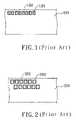
- the chip 101includes a single row of IO contact pads 102 exposed by openings in a passivation layer.
- the I/O contact pads 102are at the periphery of the chip 101 .
- Au bumps 103are formed on the I/O contact pads 102 . There are no semiconductor devices, such MOS devices or transistors, under the I/O contact pads 102 .
- the size of the Au bumps 103have to be shrunk to maintain the chip 101 in a small size. Then it becomes technically difficult and economically expensive in connecting the chip 101 to an external circuitry.
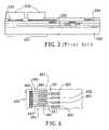
- Some designersdesign the contact pads 202 of the chip 201 aligned in two rows, as shown in FIGS. 2 and 3 , with the contact pads 202 exposed by openings in a passivation layer 204 .
- There are no semiconductor devices 205such MOS devices or transistors, under the contact pads 202 and Au bumps 203 , neither. Then the chip 201 cannot be maintained in a small size since the underlying semiconductor substrate 206 vacates a peripheral region 207 having no semiconductor devices.
- the objective of the inventionis to provide multiple metal bumps that are soft and ductile to buffer and absorb the shock energy during assembling the semiconductor chip and an external circuitry or to buffer and absorb the shock energy during a probe or testing card is poked in the metal bumps. Therefore, the invention allows the semiconductor devices under the metal bumps without being damaged if a shock happens to the metal bumps.
- Another objective of the inventionis to provide an RDL layer that is employed to change the I/O layout from a fine-pitched contact pad exposed by an opening in the passivation layer to a coarse-pitched contact pad formed over the fine-pitched contact pad or a passivation layer. Therefore, the process for forming a metal bump on the RDL layer is easily performed.
- Another objective of the inventionis to provide a semiconductor chip where a peripheral region of a semiconductor substrate close to the edge thereof may have semiconductor devices formed therein or on.
- the rate of the semiconductor devices occupying the top surface of the semiconductor substrateis improved and therefore the semiconductor chip can be shrunk.
- FIG. 1illustrates a top view of a conventional semiconductor chip.
- FIG. 2illustrates a top view of another conventional semiconductor chip.
- FIG. 3illustrates s cross-sectional view of FIG. 2 .
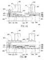
- FIG. 4illustrates a top view of a semiconductor chip according to the invention.
- FIG. 4Aillustrates a cross-sectional view of FIG. 4 .
- FIG. 4Billustrates an cross-sectional view of an alternative semiconductor chip according to the invention.
- FIGS. 5-5Aillustrate top and cross-sectional views of an alternative semiconductor chip according to the invention.
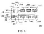
- FIG. 6illustrates a top view of an alternative semiconductor chip according to the invention.
- an embodiment of the inventionis the cross section of an semiconductor chip 400 including a semiconductor substrate 401 , such as silicon substrate, GaAs substrate or SiGe substrate, with multiple semiconductor devices 403 , such as CMOS devices, transistors, resistors, capacitors, or inductors, formed therein or on, multiple thin-film dielectric layers 408 , such as silicon oxide, over the semiconductor substrate 401 , multiple thin-film metal layers 404 , formed by a process comprising sputtering an aluminum layer and then patterning the aluminum layer, or by a process comprising electroplating a copper layer in opening in a dielectric layer and on the dielectric layer and then removing the copper layer outside the opening in the dielectric layer using a CMP process, and a passivation layer 405 over the thin-film dielectric layers 408 and thin-film metal layers 404 , multiple openings 480 in the passivation layer 405 exposing multiple contact pads 402 provided by the topmost one of the thin-film metal layers
- the openings 480have a largest transverse dimension w of between 0.1 and 30 microns, for example.
- the passivation layer 405should be thick enough to prevent moisture, impurities, mobile ions or transitional metal elements from moving through the passivation layer 405 .
- the passivation layer 405is constructed of a silicon oxide compound, a silicon nitride compound, phosphosilicate glass (PSG), a silicon oxynitride compound or a composite formed by depositing the above materials.
- the passivation layer 405can be formed by first depositing a silicon-oxide layer with a thickness of between 0.2 and 1.0 microns using a PECVD process, then depositing a silicon-nitride layer with a thickness of between 0.2 and 1.0 microns on the silicon-oxide layer using a PECVD process.
- the passivation layer 405can be formed by first depositing a silicon-oxide layer with a thickness of between 0.2 and 1.0 microns using a PECVD process, then depositing a silicon-oxynitride layer with a thickness of between 0.05 and 0.5 microns on the silicon-oxide layer using a PECVD process, and then depositing a silicon-nitride layer with a thickness of between 0.2 and 1.0 microns on the silicon-oxynitride layer using a PECVD process.
- the passivation layer 405can be formed by first depositing a silicon-oxynitride layer with a thickness of between 0.05 and 0.5 microns using a PECVD process, then depositing a silicon-oxide layer with a thickness of between 0.2 and 1.0 microns on the silicon-oxynitride layer using a PECVD process, and then depositing a silicon-nitride layer with a thickness of between 0.2 and 1.0 microns on the silicon-oxide layer using a PECVD process.
- the passivation layer 405can be formed by first depositing a silicon-oxide layer with a thickness of between 0.2 and 1.0 microns using a PECVD process, then depositing a silicon-oxide layer with a thickness of between 0.5 and 3.0 microns on the PECVD silicon-oxide layer using a spin-coating process, then depositing a silicon-oxide layer with a thickness of between 0.2 and 1.0 microns on the spin-coated silicon-oxide layer using a PECVD process, and then depositing a silicon-nitride layer with a thickness of between 0.2 and 1.0 microns on the PECVD silicon-oxide layer using a PECVD process.
- the passivation layer 405can be formed by first depositing a silicon-oxide layer with a thickness of between 0.5 and 3.0 microns using a HDP-CVD process, and then depositing a silicon-nitride layer with a thickness of between 0.2 and 1.0 microns on the silicon-oxide layer using a PECVD process.
- the passivation layer 405can be formed by first depositing a USG layer with a thickness of between 0.2 and 3 microns, then depositing a layer of TEOS, BPSG or PSG with a thickness of between 0.5 and 3 microns on the USG layer, and then depositing a silicon-nitride layer with a thickness of between 0.2 and 1.0 microns on the layer of TEOS, BPSG or PSG using a PECVD process.
- the passivation layer 405can be formed by optionally first depositing a first silicon-oxynitride layer with a thickness of between 0.05 and 0.5 microns on the silicon-oxide layer using a PECVD process, then depositing a silicon-oxide layer with a thickness of between 0.2 and 1.0 microns optionally on the first silicon-oxynitride layer using a PECVD process, then optionally depositing a second silicon-oxynitride layer with a thickness of between 0.05 and 0.5 microns on the silicon-oxide layer using a PECVD process, then depositing a silicon-nitride layer with a thickness of between 0.2 and 1.0 microns on the second silicon-oxynitride layer or on the silicon-oxide layer using a PECVD process, then optionally depositing a third silicon-oxynitride layer with a thickness of between 0.05 and 0.5 microns on the silicon-nitride layer using a PECVD process, and then depositing a third silicon
- the passivation layer 405can be formed by first depositing a first silicon-oxide layer with a thickness of between 0.2 and 1.0 microns using a PECVD process, then depositing a second silicon-oxide layer with a thickness of between 0.5 and 3.0 microns on the first silicon-oxide layer using a spin-coating process, then depositing a third silicon-oxide layer with a thickness of between 0.2 and 1.0 microns on the second silicon-oxide layer using a PECVD process, then depositing a silicon-nitride layer with a thickness of between 0.2 and 1.0 microns on the third silicon-oxide layer using a PECVD process, and then depositing a fourth silicon-oxide layer with a thickness of between 0.2 and 1.0 microns on the silicon-nitride layer using a PECVD process.
- the passivation layer 405can be formed by first depositing a silicon-oxide layer with a thickness of between 0.5 and 3.0 microns using a HDP-CVD process, then depositing a silicon-nitride layer with a thickness of between 0.2 and 1.0 microns on the silicon-oxide layer using a PECVD process, and then depositing another silicon-oxide layer with a thickness of between 0.5 and 3.0 microns on the silicon-nitride layer using a HDP-CVD process.
- a patterned metal layer 406 working as a redistribution layer (RDL)is deposited on the passivation layer 405 and connected to the contact pads 402 through the openings 480 in the passivation layer 405 .
- the redistribution layer 406includes multiple contact pads 481 and 482 used to have metal bumps 407 formed thereon.
- the contact pads 481 and 482have positions different from those of the contact pads 402 exposed by the openings 480 in the passivation layer 405 from a top view, as shown in FIG. 4 .
- FIG. 4is a top view of FIGS. 4A and 4B .
- the contact pads 481 and 482are placed close to the edge 490 of the semiconductor chip 400 .
- the contact pads 481are aligned in an external line, while the contact pads 482 are aligned in an internal line.
- Multiple traces 484 of the patterned metal layer 406 connecting the contact pads 402 exposed by the openings 480 in the passivation layer 405 to the contact pads 482 aligned in the internal linepass through the gap between the neighboring contact pads 481 aligned in the external line.
- Multiple traces 483 of the patterned metal layer 406connect the contact pads 402 exposed by the openings 480 in the passivation layer 405 to the contact pads 481 aligned in the internal line.
- the metal bumps 407are formed over the semiconductor devices 403 and thin-film metal layers 404 .
- the metal bumps 407can be connected to electrical contact pads on a glass substrate, flexible substrate, TAB (tape automated bonding) carrier or printed circuit board.
- the metal bumps 407are formed with more than 50 percent by weight of gold, for example, and preferably with more than 90 percent by weight of gold.
- the metal bumps 407have a height hi of between 8 and 50 microns and, preferably, between 10 and 30 microns.
- the contact pads 402are formed over an ESD (electrostatic discharge) circuit 403 a and connected to the ESD circuit 403 a through a metal plug 410 .
- the metal plug 410has a bottom end joined to a contact of the ESD circuit 403 a and a top end joined to the bottom of the contact pads 402 .
- FIG. 4Banother embodiment of the invention, it is almost similar to the detail in FIG. 4A except there is a polymer layer 409 formed on the passivation layer 405 and under the patterned metal layer 406 .
- the polymer layer 409may be polyimide, benzocyclobutene (BCB), silicone, Teflon, paralene or rubber.
- the polymer layer 409may be a porous structure.
- the polymer layer 409may have a thickness t 1 of between 1 and 30 microns, and, preferably, between 3 and 10 microns.
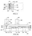
- FIGS. 5 and 5Aare an embodiment of the invention to show top and cross-sectional views of a semiconductor chip.
- the contact pads 402are placed close to the edge 490 of the semiconductor chip 400 .
- a patterned metal layer 406 including multiple contact pads 491 and 492 and traces 493is formed on the polymer layer 409 and on the contact pads 402 exposed by openings in the passivation layer 405 .
- the contact pads 491 aligned in the external lineare placed on the contact pads 402 exposed by the openings in the passivation layer 405
- the contact pads 492 aligned in the internal lineare placed not on the contact pads 402 exposed by the openings in the passivation layer 405 but on the polymer layer 409 .
- the traces 493 of the patterned metal layerconnect the contact pads 402 exposed by the openings in the passivation layer 405 to the contact pads 492 aligned in the internal line.
- Various metal bumps described in the above paragraphscan be formed on the contact pads 491 and 492 .
- the patterned metal layer 406can be formed on the passivation layer 405 without the polymer layer 409 between the patterned metal layer 406 and the passivation layer 405 .
- FIG. 6is an embodiment of the invention to show a top view of a semiconductor chip.
- the patterned metal layer formed over the passivation layer and on the contact pads exposed by the openings in the passivation layerincludes multiple contact pads 581 , 582 and 583 and traces 584 , 585 and 586 .
- the contact pads 581 , 582 and 583 used to have metal bumps formed thereoncan be aligned in three lines along an edge 490 of the semiconductor chip 500 .
- traces 586 of the patterned metal layer connecting the contact pads 402 exposed by the openings in the passivation layer to the contact pads 583 aligned in the internal linepass through the gap between the neighboring contact pads 581 aligned in the external line and the gap between the neighboring contact pads 582 aligned in the middle line.
- Multiple traces 585 of the patterned metal layer connecting the contact pads 402 exposed by the openings in the passivation layer to the contact pads 582 aligned in the middle linepass through the gap between the neighboring contact pads 581 aligned in the external line.
- the patterned metal layercan be formed on the passivation layer without the polymer layer between the patterned metal layer and the passivation layer. Alternatively, the patterned metal layer can be formed on the polymer layer deposited on the passivation layer.
- the material of the metal bumpsis soft and ductile to buffer and absorb the shock energy during assembling the semiconductor chip and an external circuitry or to buffer and absorb the shock energy during a probe or testing card is poked in the metal bumps.
- the RDL layeris employed to change the I/O layout from the fine-pitched contact pads exposed by the opening in the passivation layer to the coarse-pitched contact pads formed over the fine-pitched contact pads or the passivation layer. Therefore, the process for forming metal bumps is easily performed.
Landscapes
- Engineering & Computer Science (AREA)
- Computer Hardware Design (AREA)
- Microelectronics & Electronic Packaging (AREA)
- Power Engineering (AREA)
- Physics & Mathematics (AREA)
- Condensed Matter Physics & Semiconductors (AREA)
- General Physics & Mathematics (AREA)
- Manufacturing & Machinery (AREA)
- Internal Circuitry In Semiconductor Integrated Circuit Devices (AREA)
Abstract
Description
Claims (33)
Priority Applications (1)
| Application Number | Priority Date | Filing Date | Title |
|---|---|---|---|
| US12/464,896US8242601B2 (en) | 2004-10-29 | 2009-05-13 | Semiconductor chip with passivation layer comprising metal interconnect and contact pads |
Applications Claiming Priority (3)
| Application Number | Priority Date | Filing Date | Title |
|---|---|---|---|
| US62355304P | 2004-10-29 | 2004-10-29 | |
| US11/262,182US7547969B2 (en) | 2004-10-29 | 2005-10-28 | Semiconductor chip with passivation layer comprising metal interconnect and contact pads |
| US12/464,896US8242601B2 (en) | 2004-10-29 | 2009-05-13 | Semiconductor chip with passivation layer comprising metal interconnect and contact pads |
Related Parent Applications (1)
| Application Number | Title | Priority Date | Filing Date |
|---|---|---|---|
| US11/262,182ContinuationUS7547969B2 (en) | 2004-10-29 | 2005-10-28 | Semiconductor chip with passivation layer comprising metal interconnect and contact pads |
Publications (2)
| Publication Number | Publication Date |
|---|---|
| US20090218687A1 US20090218687A1 (en) | 2009-09-03 |
| US8242601B2true US8242601B2 (en) | 2012-08-14 |
Family
ID=36260881
Family Applications (2)
| Application Number | Title | Priority Date | Filing Date |
|---|---|---|---|
| US11/262,182Active2026-02-25US7547969B2 (en) | 2004-10-29 | 2005-10-28 | Semiconductor chip with passivation layer comprising metal interconnect and contact pads |
| US12/464,896ActiveUS8242601B2 (en) | 2004-10-29 | 2009-05-13 | Semiconductor chip with passivation layer comprising metal interconnect and contact pads |
Family Applications Before (1)
| Application Number | Title | Priority Date | Filing Date |
|---|---|---|---|
| US11/262,182Active2026-02-25US7547969B2 (en) | 2004-10-29 | 2005-10-28 | Semiconductor chip with passivation layer comprising metal interconnect and contact pads |
Country Status (1)
| Country | Link |
|---|---|
| US (2) | US7547969B2 (en) |
Cited By (4)
| Publication number | Priority date | Publication date | Assignee | Title |
|---|---|---|---|---|
| US20130049217A1 (en)* | 2011-08-31 | 2013-02-28 | Zhiwei Gong | Semiconductor device packaging having pre-encapsulation through via formation using drop-in signal conduits |
| US8597983B2 (en) | 2011-11-18 | 2013-12-03 | Freescale Semiconductor, Inc. | Semiconductor device packaging having substrate with pre-encapsulation through via formation |
| US8916421B2 (en) | 2011-08-31 | 2014-12-23 | Freescale Semiconductor, Inc. | Semiconductor device packaging having pre-encapsulation through via formation using lead frames with attached signal conduits |
| US20210287973A1 (en)* | 2019-10-18 | 2021-09-16 | Taiwan Semiconductor Manufacturing Co., Ltd. | Low-Stress Passivation Layer |
Families Citing this family (17)
| Publication number | Priority date | Publication date | Assignee | Title |
|---|---|---|---|---|
| US8021976B2 (en)* | 2002-10-15 | 2011-09-20 | Megica Corporation | Method of wire bonding over active area of a semiconductor circuit |
| US8022544B2 (en) | 2004-07-09 | 2011-09-20 | Megica Corporation | Chip structure |
| US7465654B2 (en) | 2004-07-09 | 2008-12-16 | Megica Corporation | Structure of gold bumps and gold conductors on one IC die and methods of manufacturing the structures |
| US7452803B2 (en) | 2004-08-12 | 2008-11-18 | Megica Corporation | Method for fabricating chip structure |
| US7547969B2 (en)* | 2004-10-29 | 2009-06-16 | Megica Corporation | Semiconductor chip with passivation layer comprising metal interconnect and contact pads |
| CN1901162B (en) | 2005-07-22 | 2011-04-20 | 米辑电子股份有限公司 | Method for manufacturing circuit assembly by continuous electroplating and circuit assembly structure |
| US7397121B2 (en)* | 2005-10-28 | 2008-07-08 | Megica Corporation | Semiconductor chip with post-passivation scheme formed over passivation layer |
| JPWO2007055047A1 (en)* | 2005-11-10 | 2009-04-30 | シャープ株式会社 | Display device and electronic device including the same |
| US8421227B2 (en)* | 2006-06-28 | 2013-04-16 | Megica Corporation | Semiconductor chip structure |
| US8193636B2 (en)* | 2007-03-13 | 2012-06-05 | Megica Corporation | Chip assembly with interconnection by metal bump |
| JP5361264B2 (en) | 2008-07-04 | 2013-12-04 | ローム株式会社 | Semiconductor device |
| KR20100055193A (en)* | 2008-11-17 | 2010-05-26 | 삼성전자주식회사 | Semiconductor integrated circuit device and liquid crystal display comprising the same |
| TWI528514B (en)* | 2009-08-20 | 2016-04-01 | 精材科技股份有限公司 | Chip package and fabrication method thereof |
| KR101101686B1 (en)* | 2010-01-07 | 2011-12-30 | 삼성전기주식회사 | High frequency semiconductor device and manufacturing method thereof |
| CA2882646A1 (en) | 2012-09-05 | 2014-03-13 | Research Triangle Institute | Electronic devices utilizing contact pads with protrusions and methods for fabrication |
| US10177011B2 (en)* | 2017-04-13 | 2019-01-08 | Powertech Technology Inc. | Chip packaging method by using a temporary carrier for flattening a multi-layer structure |
| US20250300146A1 (en)* | 2022-05-23 | 2025-09-25 | Massachusetts Institute Of Technology | Extremely Large Area Integrated Circuit |
Citations (121)
| Publication number | Priority date | Publication date | Assignee | Title |
|---|---|---|---|---|
| US3668484A (en) | 1970-10-28 | 1972-06-06 | Rca Corp | Semiconductor device with multi-level metalization and method of making the same |
| US4685998A (en) | 1984-03-22 | 1987-08-11 | Thomson Components - Mostek Corp. | Process of forming integrated circuits with contact pads in a standard array |
| US4825276A (en) | 1986-06-19 | 1989-04-25 | Nec Corporation | Integrated circuit semiconductor device having improved wiring structure |
| US4880708A (en)* | 1988-07-05 | 1989-11-14 | Motorola, Inc. | Metallization scheme providing adhesion and barrier properties |
| US5083187A (en) | 1990-05-16 | 1992-01-21 | Texas Instruments Incorporated | Integrated circuit device having bumped power supply buses over active surface areas and method of manufacture thereof |
| US5226232A (en) | 1990-05-18 | 1993-07-13 | Hewlett-Packard Company | Method for forming a conductive pattern on an integrated circuit |
| US5468984A (en) | 1994-11-02 | 1995-11-21 | Texas Instruments Incorporated | ESD protection structure using LDMOS diodes with thick copper interconnect |
| US5532512A (en) | 1994-10-03 | 1996-07-02 | General Electric Company | Direct stacked and flip chip power semiconductor device structures |
| US5554940A (en) | 1994-07-05 | 1996-09-10 | Motorola, Inc. | Bumped semiconductor device and method for probing the same |
| US5631499A (en) | 1994-04-28 | 1997-05-20 | Kabushiki Kaisha Toshiba | Semiconductor device comprising fine bump electrode having small side etch portion and stable characteristics |
| US5656858A (en) | 1994-10-19 | 1997-08-12 | Nippondenso Co., Ltd. | Semiconductor device with bump structure |
| US5659201A (en) | 1995-06-05 | 1997-08-19 | Advanced Micro Devices, Inc. | High conductivity interconnection line |
| US5691248A (en) | 1995-07-26 | 1997-11-25 | International Business Machines Corporation | Methods for precise definition of integrated circuit chip edges |
| US5726502A (en) | 1996-04-26 | 1998-03-10 | Motorola, Inc. | Bumped semiconductor device with alignment features and method for making the same |
| US5742094A (en) | 1993-01-25 | 1998-04-21 | Intel Corporation | Sealed semiconductor chip |
| US5792594A (en) | 1996-04-01 | 1998-08-11 | Motorola, Inc. | Metallization and termination process for an integrated circuit chip |
| US5834844A (en) | 1995-03-24 | 1998-11-10 | Shinko Electric Industries Co., Ltd. | Semiconductor device having an element with circuit pattern thereon |
| US5854513A (en) | 1995-07-14 | 1998-12-29 | Lg Electronics Inc. | Semiconductor device having a bump structure and test electrode |
| US5879964A (en) | 1997-07-07 | 1999-03-09 | Korea Advanced Institute Of Science And Technology | Method for fabricating chip size packages using lamination process |
| US5883435A (en) | 1996-07-25 | 1999-03-16 | International Business Machines Corporation | Personalization structure for semiconductor devices |
| US5895947A (en) | 1996-07-29 | 1999-04-20 | Samsung Electronics Co., Ltd. | Intergrated circuit memory devices including capacitors on capping layer |
| US6011314A (en) | 1999-02-01 | 2000-01-04 | Hewlett-Packard Company | Redistribution layer and under bump material structure for converting periphery conductive pads to an array of solder bumps |
| US6013571A (en) | 1997-06-16 | 2000-01-11 | Motorola, Inc. | Microelectronic assembly including columnar interconnections and method for forming same |
| US6022792A (en) | 1996-03-13 | 2000-02-08 | Seiko Instruments, Inc. | Semiconductor dicing and assembling method |
| US6077726A (en) | 1998-07-30 | 2000-06-20 | Motorola, Inc. | Method and apparatus for stress relief in solder bump formation on a semiconductor device |
| US6103552A (en) | 1998-08-10 | 2000-08-15 | Lin; Mou-Shiung | Wafer scale packaging scheme |
| US6107180A (en) | 1998-01-30 | 2000-08-22 | Motorola, Inc. | Method for forming interconnect bumps on a semiconductor die |
| US6144100A (en) | 1997-06-05 | 2000-11-07 | Texas Instruments Incorporated | Integrated circuit with bonding layer over active circuitry |
| US6159837A (en) | 1998-07-16 | 2000-12-12 | Kabushiki Kaisha Toshiba | Manufacturing method of semiconductor device |
| US6166444A (en) | 1999-06-21 | 2000-12-26 | United Microelectronics Corp. | Cascade-type chip module |
| US6181569B1 (en) | 1999-06-07 | 2001-01-30 | Kishore K. Chakravorty | Low cost chip size package and method of fabricating the same |
| US6184143B1 (en) | 1997-09-08 | 2001-02-06 | Hitachi, Ltd. | Semiconductor integrated circuit device and fabrication process thereof |
| US6187680B1 (en) | 1998-10-07 | 2001-02-13 | International Business Machines Corporation | Method/structure for creating aluminum wirebound pad on copper BEOL |
| US20010000080A1 (en) | 1998-03-27 | 2001-03-29 | Kazuhiko Nozawa | Semiconductor device and method of manufacturing the same, circuit board and electronic instrument |
| US6229711B1 (en) | 1998-08-31 | 2001-05-08 | Shinko Electric Industries Co., Ltd. | Flip-chip mount board and flip-chip mount structure with improved mounting reliability |
| US6287893B1 (en) | 1997-10-20 | 2001-09-11 | Flip Chip Technologies, L.L.C. | Method for forming chip scale package |
| US20010026021A1 (en) | 2000-02-21 | 2001-10-04 | Hirokazu Honda | Flip-chip type semiconductor device and method of manufacturing the same |
| US20010040290A1 (en) | 2000-05-01 | 2001-11-15 | Seiko Epson Corporation | Method for forming bump, semiconductor device and method for making the same, circuit board, and electronic device |
| US6319846B1 (en) | 2001-01-05 | 2001-11-20 | Taiwan Semiconductor Manufacturing Company, Ltd | Method for removing solder bodies from a semiconductor wafer |
| US20010051426A1 (en) | 1999-11-22 | 2001-12-13 | Scott K. Pozder | Method for forming a semiconductor device having a mechanically robust pad interface. |
| US20020016079A1 (en) | 1999-12-14 | 2002-02-07 | Dykstra Jerald P. | Enhanced etching/smoothing of dielectric surfaces |
| US6359328B1 (en) | 1998-12-31 | 2002-03-19 | Intel Corporation | Methods for making interconnects and diffusion barriers in integrated circuits |
| US6362087B1 (en) | 2000-05-05 | 2002-03-26 | Aptos Corporation | Method for fabricating a microelectronic fabrication having formed therein a redistribution structure |
| US6372619B1 (en) | 2001-07-30 | 2002-04-16 | Taiwan Semiconductor Manufacturing Company, Ltd | Method for fabricating wafer level chip scale package with discrete package encapsulation |
| US20020043723A1 (en) | 2000-10-16 | 2002-04-18 | Hironobu Shimizu | Semiconductor device and manufacturing method thereof |
| US6380061B1 (en) | 1998-12-17 | 2002-04-30 | Shinko Electric Industries Co., Ltd. | Process for fabricating bump electrode |
| US6383916B1 (en)* | 1998-12-21 | 2002-05-07 | M. S. Lin | Top layers of metal for high performance IC's |
| US20020079576A1 (en) | 2000-06-30 | 2002-06-27 | Krishna Seshan | Ball limiting metallurgy for input/outputs and methods of fabrication |
| US6426281B1 (en) | 2001-01-16 | 2002-07-30 | Taiwan Semiconductor Manufacturing Company | Method to form bump in bumping technology |
| US20020100975A1 (en) | 2001-01-29 | 2002-08-01 | Makoto Kanda | Semiconductor integrated circuit and fabrication process therefor |
| US6429120B1 (en) | 2000-01-18 | 2002-08-06 | Micron Technology, Inc. | Methods and apparatus for making integrated-circuit wiring from copper, silver, gold, and other metals |
| US6458622B1 (en) | 1999-07-06 | 2002-10-01 | Motorola, Inc. | Stress compensation composition and semiconductor component formed using the stress compensation composition |
| US6462426B1 (en) | 2000-12-14 | 2002-10-08 | National Semiconductor Corporation | Barrier pad for wafer level chip scale packages |
| US6472745B1 (en) | 1999-01-18 | 2002-10-29 | Shinko Electric Industries Co., Ltd. | Semiconductor device |
| US20020158334A1 (en) | 2001-04-30 | 2002-10-31 | Intel Corporation | Microelectronic device having signal distribution functionality on an interfacial layer thereof |
| US6479900B1 (en) | 1998-12-22 | 2002-11-12 | Sanyo Electric Co., Ltd. | Semiconductor device and method of manufacturing the same |
| US20030006062A1 (en) | 2001-07-06 | 2003-01-09 | Stone William M. | Interconnect system and method of fabrication |
| US20030008133A1 (en) | 2001-07-06 | 2003-01-09 | Korea Advanced Institute Of Science And Technology | Anisotropic conductive film and method of fabricating the same for ultra-fine pitch COG application |
| US20030020163A1 (en) | 2001-07-25 | 2003-01-30 | Cheng-Yu Hung | Bonding pad structure for copper/low-k dielectric material BEOL process |
| US6534853B2 (en) | 2001-06-05 | 2003-03-18 | Chipmos Technologies Inc. | Semiconductor wafer designed to avoid probed marks while testing |
| US20030052409A1 (en) | 2001-08-29 | 2003-03-20 | Mie Matsuo | Semiconductor device and method of manufacturing the same |
| US20030080416A1 (en) | 2001-10-29 | 2003-05-01 | Dialog Semiconductor Gmbh | Sub-milliohm on-chip interconnection |
| US20030127734A1 (en) | 2002-01-07 | 2003-07-10 | Jin-Yuan Lee | Cylindrical bonding structure and method of manufacture |
| US6596560B1 (en) | 2001-12-28 | 2003-07-22 | Via Technologies, Inc. | Method of making wafer level packaging and chip structure |
| US6605525B2 (en) | 2001-05-01 | 2003-08-12 | Industrial Technologies Research Institute | Method for forming a wafer level package incorporating a multiplicity of elastomeric blocks and package formed |
| US20030162383A1 (en) | 2002-02-22 | 2003-08-28 | Matsushita Electric Industrial Co., Ltd. | Semiconductor device and method for fabricating the same |
| US6614091B1 (en) | 2002-03-13 | 2003-09-02 | Motorola, Inc. | Semiconductor device having a wire bond pad and method therefor |
| US6617655B1 (en) | 2002-04-05 | 2003-09-09 | Fairchild Semiconductor Corporation | MOSFET device with multiple gate contacts offset from gate contact area and over source area |
| US20030168733A1 (en) | 2002-03-06 | 2003-09-11 | Seiko Epson Corporation | Integrated circuit chip, electronic device and method of manufacturing the same, and electronic instrument |
| US6620728B2 (en) | 1998-12-21 | 2003-09-16 | Megic Corporation | Top layers of metal for high performance IC's |
| US6639299B2 (en) | 2001-04-17 | 2003-10-28 | Casio Computer Co., Ltd. | Semiconductor device having a chip size package including a passive element |
| US6642136B1 (en) | 2001-09-17 | 2003-11-04 | Megic Corporation | Method of making a low fabrication cost, high performance, high reliability chip scale package |
| US6646347B2 (en) | 2001-11-30 | 2003-11-11 | Motorola, Inc. | Semiconductor power device and method of formation |
| US6653563B2 (en) | 2001-03-30 | 2003-11-25 | Intel Corporation | Alternate bump metallurgy bars for power and ground routing |
| US20030219966A1 (en) | 2002-05-21 | 2003-11-27 | St Assembly Test Services Pte Ltd | Small pitch torch bump for mounting high-performance flip-chip |
| US20030218246A1 (en) | 2002-05-22 | 2003-11-27 | Hirofumi Abe | Semiconductor device passing large electric current |
| US6664141B1 (en) | 2001-08-10 | 2003-12-16 | Lsi Logic Corporation | Method of forming metal fuses in CMOS processes with copper interconnect |
| US20040007779A1 (en) | 2002-07-15 | 2004-01-15 | Diane Arbuthnot | Wafer-level method for fine-pitch, high aspect ratio chip interconnect |
| US6683380B2 (en) | 2000-07-07 | 2004-01-27 | Texas Instruments Incorporated | Integrated circuit with bonding layer over active circuitry |
| US20040023450A1 (en) | 2001-02-08 | 2004-02-05 | Mitsuaki Katagiri | Semiconductor integrated circuit device and its manufacturing method |
| US20040029404A1 (en) | 1998-12-21 | 2004-02-12 | Megic Corporation | High performance system-on-chip passive device using post passivation process |
| US20040048202A1 (en) | 2000-08-29 | 2004-03-11 | Au Optronics Corporation | Metal bump with an insulating sidewall and method of fabricating thereof |
| US6707124B2 (en) | 1992-10-26 | 2004-03-16 | Texas Instruments Incorporated | HID land grid array packaged device having electrical and optical interconnects |
| US6707159B1 (en) | 1999-02-18 | 2004-03-16 | Rohm Co., Ltd. | Semiconductor chip and production process therefor |
| US20040070042A1 (en) | 2002-10-15 | 2004-04-15 | Megic Corporation | Method of wire bonding over active area of a semiconductor circuit |
| US6762122B2 (en) | 2001-09-27 | 2004-07-13 | Unitivie International Limited | Methods of forming metallurgy structures for wire and solder bonding |
| US20040145052A1 (en) | 2003-01-29 | 2004-07-29 | Matsushita Electric Industrial Co., Ltd. | Semiconductor device and display device using the same |
| US6780748B2 (en) | 2001-12-07 | 2004-08-24 | Hitachi, Ltd. | Method of fabricating a wafer level chip size package utilizing a maskless exposure |
| US20040166659A1 (en)* | 1998-12-21 | 2004-08-26 | Megic Corporation | Top layers of metal for high performance IC's |
| US20040188839A1 (en) | 2001-04-27 | 2004-09-30 | Fujitsu Limited | Semiconductor device and method of manufacturing the same |
| US20040253801A1 (en) | 2003-06-13 | 2004-12-16 | Aptos Corporation | Ultimate low dielectric device and method of making the same |
| US6841872B1 (en) | 2000-01-05 | 2005-01-11 | Hynix Semiconductor Inc. | Semiconductor package and fabrication method thereof |
| US20050017343A1 (en) | 2003-07-23 | 2005-01-27 | Kwon Yong-Hwan | Method of forming redistribution bump and semiconductor chip and mount structure fabricated using the same |
| US6853076B2 (en) | 2001-09-21 | 2005-02-08 | Intel Corporation | Copper-containing C4 ball-limiting metallurgy stack for enhanced reliability of packaged structures and method of making same |
| US6861762B1 (en) | 2002-05-01 | 2005-03-01 | Marvell Semiconductor Israel Ltd. | Flip chip with novel power and ground arrangement |
| US6891248B2 (en) | 2002-08-23 | 2005-05-10 | Micron Technology, Inc. | Semiconductor component with on board capacitor |
| US6900538B2 (en) | 2003-06-03 | 2005-05-31 | Micrel, Inc. | Integrating chip scale packaging metallization into integrated circuit die structures |
| EP1536469A1 (en) | 2003-11-28 | 2005-06-01 | EM Microelectronic-Marin SA | Semiconductor device with connecting bumps |
| US20050121804A1 (en) | 2003-12-08 | 2005-06-09 | Nick Kuo | Chip structure with bumps and testing pads |
| US6943440B2 (en) | 2003-09-09 | 2005-09-13 | Intel Corporation | Methods of processing thick ILD layers using spray coating or lamination for C4 wafer level thick metal integrated flow |
| US6959856B2 (en) | 2003-01-10 | 2005-11-01 | Samsung Electronics Co., Ltd. | Solder bump structure and method for forming a solder bump |
| US6963136B2 (en) | 2000-12-18 | 2005-11-08 | Renesas Technology Corporation | Semiconductor integrated circuit device |
| US20060012041A1 (en) | 2004-07-16 | 2006-01-19 | Chiu-Ming Chou | Connection between two circuitry components |
| US6998711B1 (en) | 1998-08-14 | 2006-02-14 | Micron Technology, Inc. | Method of forming a micro solder ball for use in C4 bonding process |
| US20060060961A1 (en) | 2004-07-09 | 2006-03-23 | Mou-Shiung Lin | Chip structure |
| US20060091540A1 (en) | 2004-10-29 | 2006-05-04 | Megic Corporation | Semiconductor chip with post-passivation scheme formed over passivation layer |
| US7043830B2 (en) | 2003-02-20 | 2006-05-16 | Micron Technology, Inc. | Method of forming conductive bumps |
| US7220657B2 (en) | 1999-01-27 | 2007-05-22 | Shinko Electric Industries, Co., Ltd. | Semiconductor wafer and semiconductor device provided with columnar electrodes and methods of producing the wafer and device |
| US7239028B2 (en) | 2002-08-09 | 2007-07-03 | Oki Electric Industry Co., Ltd. | Semiconductor device with signal line having decreased characteristic impedance |
| US7319277B2 (en) | 2003-05-08 | 2008-01-15 | Megica Corporation | Chip structure with redistribution traces |
| US7394164B2 (en) | 2006-07-28 | 2008-07-01 | Ultra Chip, Inc. | Semiconductor device having bumps in a same row for staggered probing |
| US7397121B2 (en) | 2005-10-28 | 2008-07-08 | Megica Corporation | Semiconductor chip with post-passivation scheme formed over passivation layer |
| US7452803B2 (en) | 2004-08-12 | 2008-11-18 | Megica Corporation | Method for fabricating chip structure |
| US7465654B2 (en) | 2004-07-09 | 2008-12-16 | Megica Corporation | Structure of gold bumps and gold conductors on one IC die and methods of manufacturing the structures |
| US7470927B2 (en) | 2005-05-18 | 2008-12-30 | Megica Corporation | Semiconductor chip with coil element over passivation layer |
| US7489037B2 (en) | 2005-04-11 | 2009-02-10 | Siliconware Precision Industries Co., Ltd. | Semiconductor device and fabrication method thereof |
| US7528495B2 (en) | 2006-07-17 | 2009-05-05 | Chipmos Technologies Inc. | Chip structure |
| US7531898B2 (en) | 2002-06-25 | 2009-05-12 | Unitive International Limited | Non-Circular via holes for bumping pads and related structures |
| US7545037B2 (en) | 2005-03-18 | 2009-06-09 | Samsung Electronics Co., Ltd. | Semiconductor chips having redistributed power/ground lines directly connected to power/ground lines of internal circuits and methods of fabricating the same |
| US7566650B2 (en) | 2005-09-23 | 2009-07-28 | Stats Chippac Ltd. | Integrated circuit solder bumping system |
| US7622364B2 (en) | 2006-08-18 | 2009-11-24 | International Business Machines Corporation | Bond pad for wafer and package for CMOS imager |
- 2005
- 2005-10-28USUS11/262,182patent/US7547969B2/enactiveActive
- 2009
- 2009-05-13USUS12/464,896patent/US8242601B2/enactiveActive
Patent Citations (128)
| Publication number | Priority date | Publication date | Assignee | Title |
|---|---|---|---|---|
| US3668484A (en) | 1970-10-28 | 1972-06-06 | Rca Corp | Semiconductor device with multi-level metalization and method of making the same |
| US4685998A (en) | 1984-03-22 | 1987-08-11 | Thomson Components - Mostek Corp. | Process of forming integrated circuits with contact pads in a standard array |
| US4825276A (en) | 1986-06-19 | 1989-04-25 | Nec Corporation | Integrated circuit semiconductor device having improved wiring structure |
| US4880708A (en)* | 1988-07-05 | 1989-11-14 | Motorola, Inc. | Metallization scheme providing adhesion and barrier properties |
| US5083187A (en) | 1990-05-16 | 1992-01-21 | Texas Instruments Incorporated | Integrated circuit device having bumped power supply buses over active surface areas and method of manufacture thereof |
| US5226232A (en) | 1990-05-18 | 1993-07-13 | Hewlett-Packard Company | Method for forming a conductive pattern on an integrated circuit |
| US6707124B2 (en) | 1992-10-26 | 2004-03-16 | Texas Instruments Incorporated | HID land grid array packaged device having electrical and optical interconnects |
| US5742094A (en) | 1993-01-25 | 1998-04-21 | Intel Corporation | Sealed semiconductor chip |
| US5631499A (en) | 1994-04-28 | 1997-05-20 | Kabushiki Kaisha Toshiba | Semiconductor device comprising fine bump electrode having small side etch portion and stable characteristics |
| US5554940A (en) | 1994-07-05 | 1996-09-10 | Motorola, Inc. | Bumped semiconductor device and method for probing the same |
| US5532512A (en) | 1994-10-03 | 1996-07-02 | General Electric Company | Direct stacked and flip chip power semiconductor device structures |
| US5656858A (en) | 1994-10-19 | 1997-08-12 | Nippondenso Co., Ltd. | Semiconductor device with bump structure |
| US5468984A (en) | 1994-11-02 | 1995-11-21 | Texas Instruments Incorporated | ESD protection structure using LDMOS diodes with thick copper interconnect |
| US5834844A (en) | 1995-03-24 | 1998-11-10 | Shinko Electric Industries Co., Ltd. | Semiconductor device having an element with circuit pattern thereon |
| US5659201A (en) | 1995-06-05 | 1997-08-19 | Advanced Micro Devices, Inc. | High conductivity interconnection line |
| US5854513A (en) | 1995-07-14 | 1998-12-29 | Lg Electronics Inc. | Semiconductor device having a bump structure and test electrode |
| US5691248A (en) | 1995-07-26 | 1997-11-25 | International Business Machines Corporation | Methods for precise definition of integrated circuit chip edges |
| US6022792A (en) | 1996-03-13 | 2000-02-08 | Seiko Instruments, Inc. | Semiconductor dicing and assembling method |
| US5792594A (en) | 1996-04-01 | 1998-08-11 | Motorola, Inc. | Metallization and termination process for an integrated circuit chip |
| US5726502A (en) | 1996-04-26 | 1998-03-10 | Motorola, Inc. | Bumped semiconductor device with alignment features and method for making the same |
| US5883435A (en) | 1996-07-25 | 1999-03-16 | International Business Machines Corporation | Personalization structure for semiconductor devices |
| US5895947A (en) | 1996-07-29 | 1999-04-20 | Samsung Electronics Co., Ltd. | Intergrated circuit memory devices including capacitors on capping layer |
| US6144100A (en) | 1997-06-05 | 2000-11-07 | Texas Instruments Incorporated | Integrated circuit with bonding layer over active circuitry |
| US6013571A (en) | 1997-06-16 | 2000-01-11 | Motorola, Inc. | Microelectronic assembly including columnar interconnections and method for forming same |
| US5879964A (en) | 1997-07-07 | 1999-03-09 | Korea Advanced Institute Of Science And Technology | Method for fabricating chip size packages using lamination process |
| US6184143B1 (en) | 1997-09-08 | 2001-02-06 | Hitachi, Ltd. | Semiconductor integrated circuit device and fabrication process thereof |
| US6287893B1 (en) | 1997-10-20 | 2001-09-11 | Flip Chip Technologies, L.L.C. | Method for forming chip scale package |
| US6107180A (en) | 1998-01-30 | 2000-08-22 | Motorola, Inc. | Method for forming interconnect bumps on a semiconductor die |
| US20010000080A1 (en) | 1998-03-27 | 2001-03-29 | Kazuhiko Nozawa | Semiconductor device and method of manufacturing the same, circuit board and electronic instrument |
| US6159837A (en) | 1998-07-16 | 2000-12-12 | Kabushiki Kaisha Toshiba | Manufacturing method of semiconductor device |
| US6077726A (en) | 1998-07-30 | 2000-06-20 | Motorola, Inc. | Method and apparatus for stress relief in solder bump formation on a semiconductor device |
| US6103552A (en) | 1998-08-10 | 2000-08-15 | Lin; Mou-Shiung | Wafer scale packaging scheme |
| US6998711B1 (en) | 1998-08-14 | 2006-02-14 | Micron Technology, Inc. | Method of forming a micro solder ball for use in C4 bonding process |
| US6229711B1 (en) | 1998-08-31 | 2001-05-08 | Shinko Electric Industries Co., Ltd. | Flip-chip mount board and flip-chip mount structure with improved mounting reliability |
| US6187680B1 (en) | 1998-10-07 | 2001-02-13 | International Business Machines Corporation | Method/structure for creating aluminum wirebound pad on copper BEOL |
| US6380061B1 (en) | 1998-12-17 | 2002-04-30 | Shinko Electric Industries Co., Ltd. | Process for fabricating bump electrode |
| US20040166659A1 (en)* | 1998-12-21 | 2004-08-26 | Megic Corporation | Top layers of metal for high performance IC's |
| US6620728B2 (en) | 1998-12-21 | 2003-09-16 | Megic Corporation | Top layers of metal for high performance IC's |
| US20040029404A1 (en) | 1998-12-21 | 2004-02-12 | Megic Corporation | High performance system-on-chip passive device using post passivation process |
| US6383916B1 (en)* | 1998-12-21 | 2002-05-07 | M. S. Lin | Top layers of metal for high performance IC's |
| US6479900B1 (en) | 1998-12-22 | 2002-11-12 | Sanyo Electric Co., Ltd. | Semiconductor device and method of manufacturing the same |
| US6359328B1 (en) | 1998-12-31 | 2002-03-19 | Intel Corporation | Methods for making interconnects and diffusion barriers in integrated circuits |
| US6472745B1 (en) | 1999-01-18 | 2002-10-29 | Shinko Electric Industries Co., Ltd. | Semiconductor device |
| US7220657B2 (en) | 1999-01-27 | 2007-05-22 | Shinko Electric Industries, Co., Ltd. | Semiconductor wafer and semiconductor device provided with columnar electrodes and methods of producing the wafer and device |
| US6011314A (en) | 1999-02-01 | 2000-01-04 | Hewlett-Packard Company | Redistribution layer and under bump material structure for converting periphery conductive pads to an array of solder bumps |
| US6707159B1 (en) | 1999-02-18 | 2004-03-16 | Rohm Co., Ltd. | Semiconductor chip and production process therefor |
| US6181569B1 (en) | 1999-06-07 | 2001-01-30 | Kishore K. Chakravorty | Low cost chip size package and method of fabricating the same |
| US6166444A (en) | 1999-06-21 | 2000-12-26 | United Microelectronics Corp. | Cascade-type chip module |
| US6458622B1 (en) | 1999-07-06 | 2002-10-01 | Motorola, Inc. | Stress compensation composition and semiconductor component formed using the stress compensation composition |
| US20010051426A1 (en) | 1999-11-22 | 2001-12-13 | Scott K. Pozder | Method for forming a semiconductor device having a mechanically robust pad interface. |
| US20020016079A1 (en) | 1999-12-14 | 2002-02-07 | Dykstra Jerald P. | Enhanced etching/smoothing of dielectric surfaces |
| US6841872B1 (en) | 2000-01-05 | 2005-01-11 | Hynix Semiconductor Inc. | Semiconductor package and fabrication method thereof |
| US6429120B1 (en) | 2000-01-18 | 2002-08-06 | Micron Technology, Inc. | Methods and apparatus for making integrated-circuit wiring from copper, silver, gold, and other metals |
| US20010026021A1 (en) | 2000-02-21 | 2001-10-04 | Hirokazu Honda | Flip-chip type semiconductor device and method of manufacturing the same |
| US20010040290A1 (en) | 2000-05-01 | 2001-11-15 | Seiko Epson Corporation | Method for forming bump, semiconductor device and method for making the same, circuit board, and electronic device |
| US6362087B1 (en) | 2000-05-05 | 2002-03-26 | Aptos Corporation | Method for fabricating a microelectronic fabrication having formed therein a redistribution structure |
| US20020079576A1 (en) | 2000-06-30 | 2002-06-27 | Krishna Seshan | Ball limiting metallurgy for input/outputs and methods of fabrication |
| US6683380B2 (en) | 2000-07-07 | 2004-01-27 | Texas Instruments Incorporated | Integrated circuit with bonding layer over active circuitry |
| US20040048202A1 (en) | 2000-08-29 | 2004-03-11 | Au Optronics Corporation | Metal bump with an insulating sidewall and method of fabricating thereof |
| US20020043723A1 (en) | 2000-10-16 | 2002-04-18 | Hironobu Shimizu | Semiconductor device and manufacturing method thereof |
| US6462426B1 (en) | 2000-12-14 | 2002-10-08 | National Semiconductor Corporation | Barrier pad for wafer level chip scale packages |
| US6963136B2 (en) | 2000-12-18 | 2005-11-08 | Renesas Technology Corporation | Semiconductor integrated circuit device |
| US6319846B1 (en) | 2001-01-05 | 2001-11-20 | Taiwan Semiconductor Manufacturing Company, Ltd | Method for removing solder bodies from a semiconductor wafer |
| US6426281B1 (en) | 2001-01-16 | 2002-07-30 | Taiwan Semiconductor Manufacturing Company | Method to form bump in bumping technology |
| US20020100975A1 (en) | 2001-01-29 | 2002-08-01 | Makoto Kanda | Semiconductor integrated circuit and fabrication process therefor |
| US20040023450A1 (en) | 2001-02-08 | 2004-02-05 | Mitsuaki Katagiri | Semiconductor integrated circuit device and its manufacturing method |
| US6653563B2 (en) | 2001-03-30 | 2003-11-25 | Intel Corporation | Alternate bump metallurgy bars for power and ground routing |
| US6639299B2 (en) | 2001-04-17 | 2003-10-28 | Casio Computer Co., Ltd. | Semiconductor device having a chip size package including a passive element |
| US20040188839A1 (en) | 2001-04-27 | 2004-09-30 | Fujitsu Limited | Semiconductor device and method of manufacturing the same |
| US20020158334A1 (en) | 2001-04-30 | 2002-10-31 | Intel Corporation | Microelectronic device having signal distribution functionality on an interfacial layer thereof |
| US6605525B2 (en) | 2001-05-01 | 2003-08-12 | Industrial Technologies Research Institute | Method for forming a wafer level package incorporating a multiplicity of elastomeric blocks and package formed |
| US6534853B2 (en) | 2001-06-05 | 2003-03-18 | Chipmos Technologies Inc. | Semiconductor wafer designed to avoid probed marks while testing |
| US20030006062A1 (en) | 2001-07-06 | 2003-01-09 | Stone William M. | Interconnect system and method of fabrication |
| US20030008133A1 (en) | 2001-07-06 | 2003-01-09 | Korea Advanced Institute Of Science And Technology | Anisotropic conductive film and method of fabricating the same for ultra-fine pitch COG application |
| US20030020163A1 (en) | 2001-07-25 | 2003-01-30 | Cheng-Yu Hung | Bonding pad structure for copper/low-k dielectric material BEOL process |
| US6372619B1 (en) | 2001-07-30 | 2002-04-16 | Taiwan Semiconductor Manufacturing Company, Ltd | Method for fabricating wafer level chip scale package with discrete package encapsulation |
| US6664141B1 (en) | 2001-08-10 | 2003-12-16 | Lsi Logic Corporation | Method of forming metal fuses in CMOS processes with copper interconnect |
| US20030052409A1 (en) | 2001-08-29 | 2003-03-20 | Mie Matsuo | Semiconductor device and method of manufacturing the same |
| US6917119B2 (en) | 2001-09-17 | 2005-07-12 | Megic Corporation | Low fabrication cost, high performance, high reliability chip scale package |
| US6642136B1 (en) | 2001-09-17 | 2003-11-04 | Megic Corporation | Method of making a low fabrication cost, high performance, high reliability chip scale package |
| US6853076B2 (en) | 2001-09-21 | 2005-02-08 | Intel Corporation | Copper-containing C4 ball-limiting metallurgy stack for enhanced reliability of packaged structures and method of making same |
| US6762122B2 (en) | 2001-09-27 | 2004-07-13 | Unitivie International Limited | Methods of forming metallurgy structures for wire and solder bonding |
| US20030080416A1 (en) | 2001-10-29 | 2003-05-01 | Dialog Semiconductor Gmbh | Sub-milliohm on-chip interconnection |
| US6646347B2 (en) | 2001-11-30 | 2003-11-11 | Motorola, Inc. | Semiconductor power device and method of formation |
| US6780748B2 (en) | 2001-12-07 | 2004-08-24 | Hitachi, Ltd. | Method of fabricating a wafer level chip size package utilizing a maskless exposure |
| US6596560B1 (en) | 2001-12-28 | 2003-07-22 | Via Technologies, Inc. | Method of making wafer level packaging and chip structure |
| US20030127734A1 (en) | 2002-01-07 | 2003-07-10 | Jin-Yuan Lee | Cylindrical bonding structure and method of manufacture |
| US20030162383A1 (en) | 2002-02-22 | 2003-08-28 | Matsushita Electric Industrial Co., Ltd. | Semiconductor device and method for fabricating the same |
| US6853078B2 (en) | 2002-02-22 | 2005-02-08 | Matsushita Electric Industrial Co., Ltd. | Semiconductor device and method for fabricating the same |
| US20030168733A1 (en) | 2002-03-06 | 2003-09-11 | Seiko Epson Corporation | Integrated circuit chip, electronic device and method of manufacturing the same, and electronic instrument |
| US6614091B1 (en) | 2002-03-13 | 2003-09-02 | Motorola, Inc. | Semiconductor device having a wire bond pad and method therefor |
| US6617655B1 (en) | 2002-04-05 | 2003-09-09 | Fairchild Semiconductor Corporation | MOSFET device with multiple gate contacts offset from gate contact area and over source area |
| US6861762B1 (en) | 2002-05-01 | 2005-03-01 | Marvell Semiconductor Israel Ltd. | Flip chip with novel power and ground arrangement |
| US20030219966A1 (en) | 2002-05-21 | 2003-11-27 | St Assembly Test Services Pte Ltd | Small pitch torch bump for mounting high-performance flip-chip |
| US6940169B2 (en) | 2002-05-21 | 2005-09-06 | Stats Chippac Ltd. | Torch bump |
| US20030218246A1 (en) | 2002-05-22 | 2003-11-27 | Hirofumi Abe | Semiconductor device passing large electric current |
| US7531898B2 (en) | 2002-06-25 | 2009-05-12 | Unitive International Limited | Non-Circular via holes for bumping pads and related structures |
| US20040007779A1 (en) | 2002-07-15 | 2004-01-15 | Diane Arbuthnot | Wafer-level method for fine-pitch, high aspect ratio chip interconnect |
| US7239028B2 (en) | 2002-08-09 | 2007-07-03 | Oki Electric Industry Co., Ltd. | Semiconductor device with signal line having decreased characteristic impedance |
| US6891248B2 (en) | 2002-08-23 | 2005-05-10 | Micron Technology, Inc. | Semiconductor component with on board capacitor |
| US20040070042A1 (en) | 2002-10-15 | 2004-04-15 | Megic Corporation | Method of wire bonding over active area of a semiconductor circuit |
| US6959856B2 (en) | 2003-01-10 | 2005-11-01 | Samsung Electronics Co., Ltd. | Solder bump structure and method for forming a solder bump |
| US20040145052A1 (en) | 2003-01-29 | 2004-07-29 | Matsushita Electric Industrial Co., Ltd. | Semiconductor device and display device using the same |
| US7043830B2 (en) | 2003-02-20 | 2006-05-16 | Micron Technology, Inc. | Method of forming conductive bumps |
| US7319277B2 (en) | 2003-05-08 | 2008-01-15 | Megica Corporation | Chip structure with redistribution traces |
| US6900538B2 (en) | 2003-06-03 | 2005-05-31 | Micrel, Inc. | Integrating chip scale packaging metallization into integrated circuit die structures |
| US20040253801A1 (en) | 2003-06-13 | 2004-12-16 | Aptos Corporation | Ultimate low dielectric device and method of making the same |
| US20050017343A1 (en) | 2003-07-23 | 2005-01-27 | Kwon Yong-Hwan | Method of forming redistribution bump and semiconductor chip and mount structure fabricated using the same |
| US7078331B2 (en) | 2003-07-23 | 2006-07-18 | Samsung Electronics Co., Ltd. | Method of forming redistribution bump and semiconductor chip and mount structure fabricated using the same |
| US6943440B2 (en) | 2003-09-09 | 2005-09-13 | Intel Corporation | Methods of processing thick ILD layers using spray coating or lamination for C4 wafer level thick metal integrated flow |
| US20060076678A1 (en) | 2003-09-09 | 2006-04-13 | Kim Sarah E | Thick metal layer integrated process flow to improve power delivery and mechanical buffering |
| US6977435B2 (en) | 2003-09-09 | 2005-12-20 | Intel Corporation | Thick metal layer integrated process flow to improve power delivery and mechanical buffering |
| EP1536469A1 (en) | 2003-11-28 | 2005-06-01 | EM Microelectronic-Marin SA | Semiconductor device with connecting bumps |
| US20050121804A1 (en) | 2003-12-08 | 2005-06-09 | Nick Kuo | Chip structure with bumps and testing pads |
| US20060060961A1 (en) | 2004-07-09 | 2006-03-23 | Mou-Shiung Lin | Chip structure |
| US7465654B2 (en) | 2004-07-09 | 2008-12-16 | Megica Corporation | Structure of gold bumps and gold conductors on one IC die and methods of manufacturing the structures |
| US20060012041A1 (en) | 2004-07-16 | 2006-01-19 | Chiu-Ming Chou | Connection between two circuitry components |
| US7452803B2 (en) | 2004-08-12 | 2008-11-18 | Megica Corporation | Method for fabricating chip structure |
| US20060091540A1 (en) | 2004-10-29 | 2006-05-04 | Megic Corporation | Semiconductor chip with post-passivation scheme formed over passivation layer |
| US7547969B2 (en) | 2004-10-29 | 2009-06-16 | Megica Corporation | Semiconductor chip with passivation layer comprising metal interconnect and contact pads |
| US7545037B2 (en) | 2005-03-18 | 2009-06-09 | Samsung Electronics Co., Ltd. | Semiconductor chips having redistributed power/ground lines directly connected to power/ground lines of internal circuits and methods of fabricating the same |
| US7489037B2 (en) | 2005-04-11 | 2009-02-10 | Siliconware Precision Industries Co., Ltd. | Semiconductor device and fabrication method thereof |
| US7470927B2 (en) | 2005-05-18 | 2008-12-30 | Megica Corporation | Semiconductor chip with coil element over passivation layer |
| US7566650B2 (en) | 2005-09-23 | 2009-07-28 | Stats Chippac Ltd. | Integrated circuit solder bumping system |
| US7397121B2 (en) | 2005-10-28 | 2008-07-08 | Megica Corporation | Semiconductor chip with post-passivation scheme formed over passivation layer |
| US7528495B2 (en) | 2006-07-17 | 2009-05-05 | Chipmos Technologies Inc. | Chip structure |
| US7394164B2 (en) | 2006-07-28 | 2008-07-01 | Ultra Chip, Inc. | Semiconductor device having bumps in a same row for staggered probing |
| US7622364B2 (en) | 2006-08-18 | 2009-11-24 | International Business Machines Corporation | Bond pad for wafer and package for CMOS imager |
Non-Patent Citations (30)
| Title |
|---|
| Bohr, M. "The New Era of Scaling in an SoC World," International Solid-State Circuits Conference (2009) pp. 23-28. |
| Bohr, M. "The New Era of Scaling in an SoC World," International Solid-State Circuits Conference (2009) Presentation Slides 1-66. |
| Edelstein, D. et al. "Full Copper Wiring in a Sub-0.25 pm CMOS ULSI Technology," Technical Digest IEEE International Electron Devices Meeting (1997) pp. 773-776. |
| Edelstein, D.C., "Advantages of Copper Interconnects," Proceedings of the 12th International IEEE VLSI Multilevel Interconnection Conference (1995) pp. 301-307. |
| Gao, X. et al. "An improved electrostatic discharge protection structure for reducing triggering voltage and parasitic capacitance," Solid-State Electronics, 27 (2003), pp. 1105-1110. |
| Geffken, R. M. "An Overview of Polyimide Use in Integrated Circuits and Packaging," Proceedings of the Third International Symposium on Ultra Large Scale Integration Science and Technology (1991) pp. 667-677. |
| Groves, R. et al. "High Q Inductors in a SiGe BiCMOS Process Utilizing a Thick Metal Process Add-on Module," Proceedings of the Bipolar/BiCMOS Circuits and Technology Meeting (1999) pp. 149-152. |
| Hu, C-K. et al. "Copper-Polyimide Wiring Technology for VLSI Circuits," Materials Research Society Symposium Proceedings VLSI V (1990) pp. 369-373. |
| Ingerly, D. et al. "Low-K Interconnect Stack with Thick Metal 9 Redistribution Layer and Cu Die Bump for 45nm High vol. Manufacturing," International Interconnect Technology Conference (2008) pp. 216-218. |
| Jenei, S. et al. "High Q Inductor Add-on Module in Thick Cu/SiLK(TM) single damascene," Proceedings from the IEEE International Interconnect Technology Conference (2001) pp. 107-109. |
| Jenei, S. et al. "High Q Inductor Add-on Module in Thick Cu/SiLK™ single damascene," Proceedings from the IEEE International Interconnect Technology Conference (2001) pp. 107-109. |
| Kumar, R. et al. "A Family of 45nm IA Processors," IEEE International Solid-State Circuits Conference, Session 3, Microprocessor Technologies, 3.2 (2009) pp. 58-59. |
| Kurd, N. et al. "Next Generation Intel® Micro-architecture (Nehalem) Clocking Architecture," Symposium on VLSI Circuits Digest of Technical Papers (2008) pp. 62-63. |
| Lee, Y-H. et al. "Effect of ESD Layout on the Assembly Yield and Reliability," International Electron Devices Meeting (2006) pp. 1-4. |
| Lin, M.S. "Post Passivation Technology(TM)-MEGIC ® Way to System Solutions," Presentation given at TSMC Technology Symposium, Japan (Oct. 1, 2003) pp. 1-32. |
| Lin, M.S. "Post Passivation Technology™—MEGIC ® Way to System Solutions," Presentation given at TSMC Technology Symposium, Japan (Oct. 1, 2003) pp. 1-32. |
| Lin, M.S. et al. "A New IC Interconnection Scheme and Design Architecture for High Performance ICs at Very Low Fabrication Cost-Post Passivation Interconnection," Proceedings of the IEEE Custom Integrated Circuits Conference (Sep. 24, 2003) pp. 533-536. |
| Lin, M.S. et al. "A New System-on-a-Chip (SOC) Technology-High Q Post Passivation Inductors," Proceedings from the 53rd Electronic Components and Technology Conference (May 30, 2003) pp. 1503-1509. |
| Luther, B. et al. "Planar Copper-Polyimide Back End of the Line Interconnections for ULSI Devices," Proceedings of the 10th International IEEE VLSI Multilevel Interconnection Conference (1993) pp. 15-21. |
| Maloney, T. et al. "Novel Clamp Circuits for IC Power Supply Protection," IEEE Transactions on Components, Packaging, and Manufacturing Technology, Part C, vol. 19, No. 3 (Jul. 1996) pp. 150-161. |
| Maloney, T. et al. "Stacked PMOS Clamps for High Voltage Power Supply Protection," Electrical Overstress/Electrostatic Discharge Symposium Proceedings (1999) pp. 70-77. |
| Master, R. et al. "Ceramic Mini-Ball Grid Array Package for High Speed Device," Proceedings from the 45th Electronic Components and Technology Conference (1995) pp. 46-50. |
| MEGIC Corp. "MEGIC way to system solutions through bumping and redistribution," (Brochure) (Feb. 6, 2004) pp. 1-3. |
| Mistry, K. et al. "A 45nm Logic Technology with High-k+ Metal Gate Transistors, Strained Silicon, 9 Cu Interconnect Layers, 193nm Dry Patterning, and 100% Pb-free Packaging," IEEE International Electron Devices Meeting (2007) pp. 247-250. |
| Roesch, W. et al. "Cycling copper flip chip interconnects," Microelectronics Reliability, 44 (2004) pp. 1047-1054. |
| Sakran, N. et al. "The Implementation of the 65nm Dual-Core 64b Merom Processor," IEEE International Solid-State Circuits Conference, Session 5, Microprocessors, 5.6 (2007) pp. 106-107, p. 590. |
| Theng, C. et al. "An Automated Tool Deployment for ESD (Electro-StaticDischarge) Correct-by-Construction Strategy in 90 nm Process," IEEE International Conference on Semiconductor Electronics (2004) pp. 61-67. |
| Venkatesan, S. et al. "A High Performance 1.8V, 0.20 pm CMOS Technology with Copper Metallization," Technical Digest IEEE International Electron Devices Meeting (1997) pp. 769-772. |
| Yeoh, A. et al. "Copper Die Bumps (First Level Interconnect) and Low-K Dielectrics in 65nm High vol. Manufacturing," Electronic Components and Technology Conference (2006) pp. 1611-1615. |
| Yeoh, T-S. "ESD Effects on Power Supply Clamps," Proceedings of the 6th International Sympoisum on Physical & Failure Analysis of Integrated Circuits (1997) pp. 121-124. |
Cited By (7)
| Publication number | Priority date | Publication date | Assignee | Title |
|---|---|---|---|---|
| US20130049217A1 (en)* | 2011-08-31 | 2013-02-28 | Zhiwei Gong | Semiconductor device packaging having pre-encapsulation through via formation using drop-in signal conduits |
| US8916421B2 (en) | 2011-08-31 | 2014-12-23 | Freescale Semiconductor, Inc. | Semiconductor device packaging having pre-encapsulation through via formation using lead frames with attached signal conduits |
| US9142502B2 (en)* | 2011-08-31 | 2015-09-22 | Zhiwei Gong | Semiconductor device packaging having pre-encapsulation through via formation using drop-in signal conduits |
| US8597983B2 (en) | 2011-11-18 | 2013-12-03 | Freescale Semiconductor, Inc. | Semiconductor device packaging having substrate with pre-encapsulation through via formation |
| US20210287973A1 (en)* | 2019-10-18 | 2021-09-16 | Taiwan Semiconductor Manufacturing Co., Ltd. | Low-Stress Passivation Layer |
| US11670573B2 (en)* | 2019-10-18 | 2023-06-06 | Taiwan Semiconductor Manufacturing Co., Ltd. | Low-stress passivation layer |
| US11996356B2 (en) | 2019-10-18 | 2024-05-28 | Taiwan Semiconductor Manufacturing Co., Ltd. | Low-stress passivation layer |
Also Published As
| Publication number | Publication date |
|---|---|
| US7547969B2 (en) | 2009-06-16 |
| US20090218687A1 (en) | 2009-09-03 |
| US20060091540A1 (en) | 2006-05-04 |
Similar Documents
| Publication | Publication Date | Title |
|---|---|---|
| US8242601B2 (en) | Semiconductor chip with passivation layer comprising metal interconnect and contact pads | |
| US7397121B2 (en) | Semiconductor chip with post-passivation scheme formed over passivation layer | |
| US7397127B2 (en) | Bonding and probing pad structures | |
| US7233075B2 (en) | Bonding pad structure | |
| US6921979B2 (en) | Semiconductor device having a bond pad and method therefor | |
| US7626276B2 (en) | Method and apparatus for providing structural support for interconnect pad while allowing signal conductance | |
| US7977803B2 (en) | Chip structure with bumps and testing pads | |
| US7521812B2 (en) | Method of wire bonding over active area of a semiconductor circuit | |
| US6846717B2 (en) | Semiconductor device having a wire bond pad and method therefor | |
| US8072076B2 (en) | Bond pad structures and integrated circuit chip having the same | |
| US20070087544A1 (en) | Method for forming improved bump structure | |
| US10658325B2 (en) | Semiconductor device including a buffer layer structure for reducing stress | |
| KR100916721B1 (en) | Semiconductor device | |
| US7288845B2 (en) | Fabrication of wire bond pads over underlying active devices, passive devices and/or dielectric layers in integrated circuits | |
| US20140361433A1 (en) | Semiconductor device | |
| US20070075424A1 (en) | Semiconductor chip and semiconductor device | |
| US20070138638A1 (en) | Semiconductor device | |
| US8669555B2 (en) | Semiconductor device | |
| US7576424B2 (en) | Semiconductor device | |
| US7847385B1 (en) | Stacked die structure with an underlying copper-topped die | |
| US20080006950A1 (en) | Bonding pad structure for electronic device |
Legal Events
| Date | Code | Title | Description |
|---|---|---|---|
| AS | Assignment | Owner name:MEGICA CORPORATION, TAIWAN Free format text:ASSIGNMENT OF ASSIGNORS INTEREST;ASSIGNORS:CHOU, CHIU-MING;CHOU, CHIEN-KANG;LIN, CHING-SAN;AND OTHERS;REEL/FRAME:022674/0726 Effective date:20051025 | |
| FEPP | Fee payment procedure | Free format text:PAYOR NUMBER ASSIGNED (ORIGINAL EVENT CODE: ASPN); ENTITY STATUS OF PATENT OWNER: LARGE ENTITY | |
| STCF | Information on status: patent grant | Free format text:PATENTED CASE | |
| AS | Assignment | Owner name:MEGIT ACQUISITION CORP., CALIFORNIA Free format text:MERGER;ASSIGNOR:MEGICA CORPORATION;REEL/FRAME:031283/0198 Effective date:20130611 | |
| AS | Assignment | Owner name:QUALCOMM INCORPORATED, CALIFORNIA Free format text:ASSIGNMENT OF ASSIGNORS INTEREST;ASSIGNOR:MEGIT ACQUISITION CORP.;REEL/FRAME:033303/0124 Effective date:20140709 | |
| FPAY | Fee payment | Year of fee payment:4 | |
| MAFP | Maintenance fee payment | Free format text:PAYMENT OF MAINTENANCE FEE, 8TH YEAR, LARGE ENTITY (ORIGINAL EVENT CODE: M1552); ENTITY STATUS OF PATENT OWNER: LARGE ENTITY Year of fee payment:8 | |
| MAFP | Maintenance fee payment | Free format text:PAYMENT OF MAINTENANCE FEE, 12TH YEAR, LARGE ENTITY (ORIGINAL EVENT CODE: M1553); ENTITY STATUS OF PATENT OWNER: LARGE ENTITY Year of fee payment:12 |