US8242522B1 - Optical device structure using non-polar GaN substrates and growth structures for laser applications in 481 nm - Google Patents
Optical device structure using non-polar GaN substrates and growth structures for laser applications in 481 nmDownload PDFInfo
- Publication number
- US8242522B1 US8242522B1US12/778,718US77871810AUS8242522B1US 8242522 B1US8242522 B1US 8242522B1US 77871810 AUS77871810 AUS 77871810AUS 8242522 B1US8242522 B1US 8242522B1
- Authority
- US
- United States
- Prior art keywords
- layer
- type
- thickness
- laser
- overlying
- Prior art date
- Legal status (The legal status is an assumption and is not a legal conclusion. Google has not performed a legal analysis and makes no representation as to the accuracy of the status listed.)
- Expired - Fee Related, expires
Links
Images

Classifications
- H—ELECTRICITY
- H01—ELECTRIC ELEMENTS
- H01S—DEVICES USING THE PROCESS OF LIGHT AMPLIFICATION BY STIMULATED EMISSION OF RADIATION [LASER] TO AMPLIFY OR GENERATE LIGHT; DEVICES USING STIMULATED EMISSION OF ELECTROMAGNETIC RADIATION IN WAVE RANGES OTHER THAN OPTICAL
- H01S5/00—Semiconductor lasers
- H01S5/30—Structure or shape of the active region; Materials used for the active region
- H01S5/34—Structure or shape of the active region; Materials used for the active region comprising quantum well or superlattice structures, e.g. single quantum well [SQW] lasers, multiple quantum well [MQW] lasers or graded index separate confinement heterostructure [GRINSCH] lasers
- H01S5/343—Structure or shape of the active region; Materials used for the active region comprising quantum well or superlattice structures, e.g. single quantum well [SQW] lasers, multiple quantum well [MQW] lasers or graded index separate confinement heterostructure [GRINSCH] lasers in AIIIBV compounds, e.g. AlGaAs-laser, InP-based laser
- H01S5/34333—Structure or shape of the active region; Materials used for the active region comprising quantum well or superlattice structures, e.g. single quantum well [SQW] lasers, multiple quantum well [MQW] lasers or graded index separate confinement heterostructure [GRINSCH] lasers in AIIIBV compounds, e.g. AlGaAs-laser, InP-based laser with a well layer based on Ga(In)N or Ga(In)P, e.g. blue laser
- B—PERFORMING OPERATIONS; TRANSPORTING
- B82—NANOTECHNOLOGY
- B82Y—SPECIFIC USES OR APPLICATIONS OF NANOSTRUCTURES; MEASUREMENT OR ANALYSIS OF NANOSTRUCTURES; MANUFACTURE OR TREATMENT OF NANOSTRUCTURES
- B82Y20/00—Nanooptics, e.g. quantum optics or photonic crystals
- H—ELECTRICITY
- H01—ELECTRIC ELEMENTS
- H01S—DEVICES USING THE PROCESS OF LIGHT AMPLIFICATION BY STIMULATED EMISSION OF RADIATION [LASER] TO AMPLIFY OR GENERATE LIGHT; DEVICES USING STIMULATED EMISSION OF ELECTROMAGNETIC RADIATION IN WAVE RANGES OTHER THAN OPTICAL
- H01S5/00—Semiconductor lasers
- H01S5/30—Structure or shape of the active region; Materials used for the active region
- H01S5/32—Structure or shape of the active region; Materials used for the active region comprising PN junctions, e.g. hetero- or double- heterostructures
- H01S5/3202—Structure or shape of the active region; Materials used for the active region comprising PN junctions, e.g. hetero- or double- heterostructures grown on specifically orientated substrates, or using orientation dependent growth
- H01S5/32025—Structure or shape of the active region; Materials used for the active region comprising PN junctions, e.g. hetero- or double- heterostructures grown on specifically orientated substrates, or using orientation dependent growth non-polar orientation
- H—ELECTRICITY
- H01—ELECTRIC ELEMENTS
- H01S—DEVICES USING THE PROCESS OF LIGHT AMPLIFICATION BY STIMULATED EMISSION OF RADIATION [LASER] TO AMPLIFY OR GENERATE LIGHT; DEVICES USING STIMULATED EMISSION OF ELECTROMAGNETIC RADIATION IN WAVE RANGES OTHER THAN OPTICAL
- H01S5/00—Semiconductor lasers
- H01S5/02—Structural details or components not essential to laser action
- H01S5/0201—Separation of the wafer into individual elements, e.g. by dicing, cleaving, etching or directly during growth
- H01S5/0202—Cleaving
- H—ELECTRICITY
- H01—ELECTRIC ELEMENTS
- H01S—DEVICES USING THE PROCESS OF LIGHT AMPLIFICATION BY STIMULATED EMISSION OF RADIATION [LASER] TO AMPLIFY OR GENERATE LIGHT; DEVICES USING STIMULATED EMISSION OF ELECTROMAGNETIC RADIATION IN WAVE RANGES OTHER THAN OPTICAL
- H01S5/00—Semiconductor lasers
- H01S5/20—Structure or shape of the semiconductor body to guide the optical wave ; Confining structures perpendicular to the optical axis, e.g. index or gain guiding, stripe geometry, broad area lasers, gain tailoring, transverse or lateral reflectors, special cladding structures, MQW barrier reflection layers
- H01S5/2004—Confining in the direction perpendicular to the layer structure
- H01S5/2009—Confining in the direction perpendicular to the layer structure by using electron barrier layers
- H—ELECTRICITY
- H01—ELECTRIC ELEMENTS
- H01S—DEVICES USING THE PROCESS OF LIGHT AMPLIFICATION BY STIMULATED EMISSION OF RADIATION [LASER] TO AMPLIFY OR GENERATE LIGHT; DEVICES USING STIMULATED EMISSION OF ELECTROMAGNETIC RADIATION IN WAVE RANGES OTHER THAN OPTICAL
- H01S5/00—Semiconductor lasers
- H01S5/20—Structure or shape of the semiconductor body to guide the optical wave ; Confining structures perpendicular to the optical axis, e.g. index or gain guiding, stripe geometry, broad area lasers, gain tailoring, transverse or lateral reflectors, special cladding structures, MQW barrier reflection layers
- H01S5/2004—Confining in the direction perpendicular to the layer structure
- H01S5/2018—Optical confinement, e.g. absorbing-, reflecting- or waveguide-layers
- H01S5/2031—Optical confinement, e.g. absorbing-, reflecting- or waveguide-layers characterized by special waveguide layers, e.g. asymmetric waveguide layers or defined bandgap discontinuities
- H—ELECTRICITY
- H01—ELECTRIC ELEMENTS
- H01S—DEVICES USING THE PROCESS OF LIGHT AMPLIFICATION BY STIMULATED EMISSION OF RADIATION [LASER] TO AMPLIFY OR GENERATE LIGHT; DEVICES USING STIMULATED EMISSION OF ELECTROMAGNETIC RADIATION IN WAVE RANGES OTHER THAN OPTICAL
- H01S5/00—Semiconductor lasers
- H01S5/20—Structure or shape of the semiconductor body to guide the optical wave ; Confining structures perpendicular to the optical axis, e.g. index or gain guiding, stripe geometry, broad area lasers, gain tailoring, transverse or lateral reflectors, special cladding structures, MQW barrier reflection layers
- H01S5/22—Structure or shape of the semiconductor body to guide the optical wave ; Confining structures perpendicular to the optical axis, e.g. index or gain guiding, stripe geometry, broad area lasers, gain tailoring, transverse or lateral reflectors, special cladding structures, MQW barrier reflection layers having a ridge or stripe structure
- H01S5/2201—Structure or shape of the semiconductor body to guide the optical wave ; Confining structures perpendicular to the optical axis, e.g. index or gain guiding, stripe geometry, broad area lasers, gain tailoring, transverse or lateral reflectors, special cladding structures, MQW barrier reflection layers having a ridge or stripe structure in a specific crystallographic orientation
- H—ELECTRICITY
- H01—ELECTRIC ELEMENTS
- H01S—DEVICES USING THE PROCESS OF LIGHT AMPLIFICATION BY STIMULATED EMISSION OF RADIATION [LASER] TO AMPLIFY OR GENERATE LIGHT; DEVICES USING STIMULATED EMISSION OF ELECTROMAGNETIC RADIATION IN WAVE RANGES OTHER THAN OPTICAL
- H01S5/00—Semiconductor lasers
- H01S5/30—Structure or shape of the active region; Materials used for the active region
- H01S5/32—Structure or shape of the active region; Materials used for the active region comprising PN junctions, e.g. hetero- or double- heterostructures
- H01S5/3211—Structure or shape of the active region; Materials used for the active region comprising PN junctions, e.g. hetero- or double- heterostructures characterised by special cladding layers, e.g. details on band-discontinuities
Definitions
- This inventionis directed to optical devices and related methods. More particularly, the invention provides a method and device for emitting electromagnetic radiation using non-polar gallium containing substrates, such as GaN, MN, InN, InGaN, AlGaN, and AlInGaN, and others.
- non-polar gallium containing substratessuch as GaN, MN, InN, InGaN, AlGaN, and AlInGaN, and others.
- the inventioncan be applied to optical devices, lasers, light emitting diodes, solar cells, photoelectrochemical water splitting and hydrogen generation, photodetectors, integrated circuits, and transistors, among other devices.
- the conventional light bulbcommonly called the “Edison bulb,” has been used for over one hundred years for a variety of applications, including lighting and displays.
- the conventional light bulbuses a tungsten filament enclosed in a glass bulb sealed in a base, which is screwed into a socket.
- the socketis coupled to an AC power or DC power source.
- Such light bulbscan be found commonly in houses, buildings, and outdoor lighting displays, as well as elsewhere.
- the conventional light bulbdissipates considerable energy as thermal energy. More than 90% of the energy used for the conventional light bulb is lost as thermal energy. Secondly, reliability is a concern. The conventional light bulb routinely fails from thermal expansion and contraction of the filament element. Furthermore, light bulbs emit light over a broad spectrum, much of which does not result in bright illumination due to the spectral sensitivity of the human eye. Another disadvantage is that light bulbs emit light in all directions. Therefore they are not ideal for applications requiring directionality or focus, such as projection displays, optical data storage, or specialized directed lighting.
- the Ar-ion laserutilized a noble gas as the active medium and produced laser light output in the UV, blue, and green wavelengths including 351 nm, 454.6 nm, 457.9 nm, 465.8 nm, 476.5 nm, 488.0 nm, 496.5 nm, 501.7 nm, 514.5 nm, and 528.7 nm.
- the Ar-ion laserhad the benefit of producing highly directional and focusable light with a narrow spectral output, but the wall plug efficiency was ⁇ 0.1%. In addition, the size, weight, and cost of the lasers were undesirable.
- lamp pumped solid state laserswere developed in the infrared, with the output wavelength was converted to the visible using specialty crystals with nonlinear optical properties.
- a green lamp pumped solid state laserhad 3 stages: electricity powers lamp, lamp excites gain crystal which lases at 1064 nm, 1064 nm goes into frequency conversion crystal which converts to visible 532 nm.
- the resulting green and blue laserswere called “lamped pumped solid state lasers with second harmonic generation” (LPSS with SHG) had wall plug efficiency of ⁇ 1%, and were more efficient than Ar-ion gas lasers, but were still too inefficient, large, expensive, fragile for broad deployment outside of specialty scientific and medical applications. Additionally, the gain crystal used in the solid state lasers typically had energy storage properties which made the lasers difficult to modulate at high speeds which limited its broader deployment.
- DPSS with SHGdiode pumped solid state lasers with SHG
- the DPSS laser technologyextended the life and improved the wall plug efficiency of the LPSS lasers to 5-10%. Further commercialization resulted in more high end specialty industrial, medical, and scientific applications.
- the change to diode pumpingincreases the system cost and requires precise temperature control.
- the resulting laseris large, consumes substantial power, yet does not address the energy storage properties which make the lasers difficult to modulate at high speeds.
- the present inventionprovides a method and device for emitting electromagnetic radiation using non-polar gallium containing substrates, such as GaN, MN, InN, InGaN, AlGaN, and AlInGaN, and others.
- the inventioncan be applied to optical devices, lasers, light emitting diodes, solar cells, photoelectrochemical water splitting and hydrogen generation, photodetectors, integrated circuits, and transistors, among other devices.
- the present inventionprovides an optical device.
- the optical devicehas a gallium nitride substrate member having a non-polar crystalline surface region.
- the devicehas an n-type GaN cladding layer overlying the surface region.
- the n-type GaN cladding layerpreferably has a thickness from 100 nm to 3000 nm, with a silicon doping level of 5E17 to 3E18 cm-3.
- the devicehas an n-side SCH layer overlying the n-type GaN cladding layer.
- the n-side SCH layeris comprised of InGaN with a molar fraction of indium of between 4% and 6% and has a thickness from 45 to 60 nm.
- the devicealso has a multiple quantum well active region overlying the n-side SCH layer.
- the multiple quantum well active regionis comprised of five 4.5-5.5 nm InGaN quantum wells separated by four 9.5-10.5 nm InGaN barriers with an indium molar fraction of between 1.5% and 3%.
- the optical devicealso has a p-side guide layer overlying the multiple quantum well active region.
- the p-side guide layeris comprised of GaN with molar a thickness from 10 nm to 20 nm.
- the devicealso has an electron blocking layer overlying the p-side guide layer.
- the p-side guide layeris comprised of AlGaN with molar fraction of aluminum of between 15% and 22% and has a thickness from 10 nm to 15 nm and doped with magnesium.
- the devicefurther has a p-GaN cladding layer overlying the electron blocking layer.
- the p-GaN cladding layerhas a thickness from 400 nm to 1000 nm with Mg doping level of 5E17 cm-3 to 1E19 cm-3.
- the devicehas a p++-GaN contact layer overlying the p-GaN cladding layer.
- the p++-gaN contact layerhas a thickness from 20 nm to 40 nm with a magnesium doping level of 1E20 cm-3 to 1E21 cm-3.
- the present inventionenables a cost-effective optical device for laser applications.
- the optical devicecan be manufactured in a relatively simple and cost effective manner.
- the present apparatus and methodcan be manufactured using conventional materials and/or methods.
- the present laser deviceuses a non-polar gallium nitride material capable of achieving a 481 nm light.
- FIG. 1is a simplified perspective view of a laser device fabricated on a non-polar substrate according to an embodiment of the present invention.
- FIG. 2is a detailed cross-sectional view of a laser device fabricated on a non-polar substrate according to an embodiment of the present invention.
- FIGS. 3A and 3Bare simplified diagrams illustrating a laser device for a laser device according to an embodiment of the present invention.
- the present inventionprovides a method and device for emitting electromagnetic radiation using non-polar gallium containing substrates such as GaN, MN, InN, InGaN, AlGaN, and AlInGaN, and others.
- non-polar gallium containing substratessuch as GaN, MN, InN, InGaN, AlGaN, and AlInGaN, and others.
- the inventioncan be applied to optical devices, lasers, light emitting diodes, solar cells, photoelectrochemical water splitting and hydrogen generation, photodetectors, integrated circuits, and transistors, among other devices.
- the present laser devicecan be employed in a non-polar gallium containing substrate, as described below.
- FIG. 1is a simplified perspective view of a laser device fabricated on a non-polar substrate according to an embodiment of the present invention.
- the optical deviceincludes a gallium nitride substrate member having a non-polar crystalline surface region.
- the gallium nitride substrate memberis a bulk GaN substrate characterized by having a non-polar crystalline surface region, but can be others.
- the bulk nitride GaN substratecomprises nitrogen and has a surface dislocation density below 10 5 cm ⁇ 2 .
- the nitride crystal or wafermay comprise Al x In y Ga 1-x-y N, where 0 ⁇ x, y, x+y ⁇ 1.
- the nitride crystalcomprises GaN.
- the GaN substratehas threading dislocations, at a concentration between about 10 5 cm ⁇ 2 and about 10 8 cm ⁇ 2 , in a direction that is substantially orthogonal or oblique with respect to the surface. As a consequence of the orthogonal or oblique orientation of the dislocations, the surface dislocation density is below about 10 5 cm ⁇ 2 .
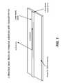
- the devicehas a laser stripe region formed overlying a portion of the non-polar crystalline orientation surface region.
- the laser stripe regionis characterized by a cavity orientation is substantially parallel to the c-direction.
- the laser strip regionhas a first end and a second end.
- the non-polar crystalline orientationis configured on an m-plane, which leads to polarization ratios parallel to the a-direction.
- the m-planeis the (10-10) family.
- there cavity orientationcan also be substantially parallel to the a-direction as well.
- the devicehas a first cleaved c-face facet provided on the first end of the laser stripe region and a second cleaved c-face facet provided on the second end of the laser stripe region.
- the first cleaved c-facetis substantially parallel with the second cleaved c-facet.
- the non-polar substrateis configured on (10-10) series of planes, which enables the formation of c-facets for laser cavities oriented in the c-direction.
- Mirror surfacesare formed on each of the cleaved surfaces.
- the first cleaved c-facetcomprises a first mirror surface.
- the first mirror surfaceis provided by a scribing and breaking process.
- the scribing processcan use any suitable techniques, such as a diamond scribe or laser scribe or combinations.
- the first mirror surfacecomprises a reflective coating.
- the reflective coatingis selected from silicon dioxide, hafnia, and titaniatantalum pentoxidezirconia, including combinations, and the like.
- the first mirror surfacecan also comprise an anti-reflective coating.
- the second cleaved c-facetcomprises a second mirror surface.
- the second mirror surfaceis provided by a scribing and breaking process according to a specific embodiment.
- the scribingis diamond scribed or laser scribed or the like.
- the second mirror surfacecomprises a reflective coating, such as silicon dioxide, hafnia, and titaniatantalum pentoxidezirconia, combinations, and the like.
- the second mirror surfacecomprises an anti-reflective coating.
- the laser stripehas a length and width.
- the lengthranges from about 50 microns to about 3000 microns.
- the stripalso has a width ranging from about 0.5 microns to about 50 microns, but can be other dimensions.
- the widthis substantially constant in dimension, although there may be slight variations.
- the width and lengthare often formed using a masking and etching process, which are commonly used in the art. Further details of the present device can be found throughout the present specification and more particularly below
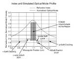
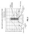
- the deviceis also characterized by a spontaneously emitted light that is polarized parallel to the a-direction. That is, the device performs as a laser or the like.
- the spontaneously emitted lightis characterized by a polarization ratio of greater than about 0.1 and less than about 1 parallel to the projection of the c-direction.
- a polarization ratioof greater than about 0.1 and less than about 1 parallel to the projection of the c-direction.
- FIG. 2is a detailed cross-sectional view of a laser device 200 fabricated on a non-polar substrate according to an embodiment of the present invention.
- the laser deviceincludes gallium nitride substrate 203, which has an underlying n-type metal back contact region 201.
- the metal back contact regionis made of a suitable material such as those noted below and others. Further details of the contact region can be found throughout the present specification and more particularly below.
- the devicealso has an overlying n-type gallium nitride layer 205, an active region 207, and an overlying p-type gallium nitride layer structured as a laser stripe region 209.
- each of these regionsis formed using at least an epitaxial deposition technique of metal organic chemical vapor deposition (MOCVD), molecular beam epitaxy (MBE), or other epitaxial growth techniques suitable for GaN growth.
- the epitaxial layeris a high quality epitaxial layer overlying the n-type gallium nitride layer.
- the high quality layeris doped, for example, with Si or O to form n-type material, with a dopant concentration between about 10 16 cm ⁇ 3 and 10 20 cm ⁇ 3 .
- an n-type Al u In v Ga 1-u-v N layerwhere 0 ⁇ u, v, u+v ⁇ 1, is deposited on the substrate.
- the carrier concentrationmay lie in the range between about 10 16 cm ⁇ 3 and 10 20 cm ⁇ 3 .
- the depositionmay be performed using metalorganic chemical vapor deposition (MOCVD) or molecular beam epitaxy (MBE).
- MOCVDmetalorganic chemical vapor deposition
- MBEmolecular beam epitaxy
- the bulk GaN substrateis placed on a susceptor in an MOCVD reactor.
- the susceptoris heated to a temperature between about 1000 and about 1200 degrees Celsius in the presence of a nitrogen-containing gas.
- the susceptoris heated to approximately 1100 degrees Celsius under flowing ammonia.
- a flow of a gallium-containing metalorganic precursor, such as trimethylgallium (TMG) or triethylgallium (TEG)is initiated, in a carrier gas, at a total rate between approximately 1 and 50 standard cubic centimeters per minute (sccm).
- the carrier gasmay comprise hydrogen, helium, nitrogen, or argon.
- the ratio of the flow rate of the group V precursor (ammonia) to that of the group III precursor (trimethylgallium, triethylgallium, trimethylindium, trimethylaluminum) during growthis between about 2000 and about 12000.
- the laser stripe regionis made of the p-type gallium nitride layer 209.
- the laser stripeis provided by an etching process selected from dry etching or wet etching.
- the etching processis dry, but can be others.
- the dry etching processis an inductively coupled process using chlorine bearing species or a reactive ion etching process using similar chemistries. Again as an example, the chlorine bearing species are commonly derived from chlorine gas or the like.
- the devicealso has an overlying dielectric region, which exposes 213 contact region.
- the dielectric regionis an oxide such as silicon dioxide or silicon nitride, but can be others.
- the contact regionis coupled to an overlying metal layer 215.
- the overlying metal layeris a multilayered structure containing gold and platinum (Pt/Au), but can be others. Of course, there can be other variations, modifications, and alternatives.
- the laser devicehas active region 207.
- the active regioncan include one to twenty quantum well regions according to one or more embodiments.
- an active layeris deposited.
- the active layermay comprise a single quantum well or a multiple quantum well, with 1-20 quantum wells.
- the quantum wellsmay comprise InGaN wells and GaN barrier layers.
- the well layers and barrier layerscomprise Al w In x Ga 1-w-x N and Al y In z Ga 1-y-z N, respectively, where 0 ⁇ w, x, y, z, w+x, y+z ⁇ 1, where w ⁇ u, y and/or x>v, z so that the bandgap of the well layer(s) is less than that of the barrier layer(s) and the n-type layer.
- the well layers and barrier layersmay each have a thickness between about 1 nm and about 40 nm.
- the active layercomprises a double heterostructure, with an InGaN or Al w In x Ga 1-w-x N layer about 10 nm to 100 nm thick surrounded by GaN or Al y In z Ga 1-y-z N layers, where w ⁇ u, y and/or x>v, z.
- the composition and structure of the active layerare chosen to provide light emission at a preselected wavelength.
- the active layermay be left undoped (or unintentionally doped) or may be doped n-type or p-type.
- the active regioncan also include an electron blocking region, and a separate confinement heterostructure.
- an electron blocking layeris preferably deposited.
- the electron-blocking layermay comprise Al s In t Ga 1-s-t N, where 0 ⁇ s, t, s+t ⁇ 1, with a higher bandgap than the active layer, and may be doped p-type.
- the electron blocking layercomprises AlGaN.
- the electron blocking layercomprises an AlGaN/GaN super-lattice structure, comprising alternating layers of AlGaN and GaN, each with a thickness between about 0.2 nm and about 5 nm.
- the p-type gallium nitride structurewhich can be a p-type doped Al q In r Ga 1-q-4 N, where 0 ⁇ q, r, q+r ⁇ 1, layer is deposited above the active layer.
- the p-type layermay be doped with Mg, to a level between about 10 16 cm ⁇ 3 and 10 22 cm ⁇ 3 , and may have a thickness between about 5 nm and about 1000 nm.
- the outermost 1-50 nm of the p-type layermay be doped more heavily than the rest of the layer, so as to enable an improved electrical contact.
- the laser stripeis provided by an etching process selected from dry etching or wet etching.
- the etching processis dry, but can be others.
- the devicealso has an overlying dielectric region, which exposes 213 contact region.
- the dielectric regionis an oxide such as silicon dioxide, but can be others.
- oxidesuch as silicon dioxide
- the metal contactis made of suitable material.
- the reflective electrical contactmay comprise at least one of silver, gold, aluminum, nickel, platinum, rhodium, palladium, chromium, or the like.
- the electrical contactmay be deposited by thermal evaporation, electron beam evaporation, electroplating, sputtering, or another suitable technique.
- the electrical contactserves as a p-type electrode for the optical device.
- the electrical contactserves as an n-type electrode for the optical device.
- the present inventionprovides an alternative device structure capable of emitting 481 nm light, among others, in a ridge laser embodiment.
- the deviceis provided with one or more of the following elements, as also referenced in FIGS. 3A and 3B .
- n-GaN cladding layerwith a thickness from 100 nm to 3000 nm with Si doping level of 5E17 to 3E18 cm-3
- n-side SCH layercomprised of InGaN with molar fraction of indium of between 4% and 6% and thickness from 45 to 60 nm
- Multiple quantum well active region layerscomprised of five 4.5-5.5 nm InGaN quantum wells separated by four 9.5-10.5 nm InGaN barriers with an indium molar fraction of between 1.5% and 3%
- p-side guide layercomprised of GaN with molar a thickness from 10 nm to 20 nm.
- Electron blocking layercomprised of AlGaN with molar fraction of aluminum of between 15% and 22% and thickness from 10 nm to 15 nm and doped with Mg.
- p-GaN cladding layerwith a thickness from 400 nm to 1000 nm with Mg doping level of 5E17 cm-3 to 1E19 cm-3
- p++-GaN contact layerwith a thickness from 20 nm to 40 nm with Mg doping level of 1E20 cm-3 to 1E21 cm-3
- the laser deviceis fabricated on a non-polar oriented surface region (m-plane).
- the non-polar substratehas a miscut or off cut of ⁇ 0.8 to ⁇ 1.2 degrees towards (0001) and ⁇ 0.3 to 0.3 degrees towards (11-20).
- the non-polar oriented surface regionhas an overlying n-GaN/p-GaN grown with H 2 /N 2 subflow and H 2 carrier gas.
Landscapes
- Physics & Mathematics (AREA)
- Optics & Photonics (AREA)
- Condensed Matter Physics & Semiconductors (AREA)
- General Physics & Mathematics (AREA)
- Electromagnetism (AREA)
- Chemical & Material Sciences (AREA)
- Engineering & Computer Science (AREA)
- Nanotechnology (AREA)
- Life Sciences & Earth Sciences (AREA)
- Biophysics (AREA)
- Crystallography & Structural Chemistry (AREA)
- Semiconductor Lasers (AREA)
Abstract
Description
Claims (1)
Priority Applications (12)
| Application Number | Priority Date | Filing Date | Title |
|---|---|---|---|
| US12/778,718US8242522B1 (en) | 2009-05-12 | 2010-05-12 | Optical device structure using non-polar GaN substrates and growth structures for laser applications in 481 nm |
| US13/549,335US8837545B2 (en) | 2009-04-13 | 2012-07-13 | Optical device structure using GaN substrates and growth structures for laser applications |
| US14/229,738US8969113B2 (en) | 2009-04-13 | 2014-03-28 | Optical device structure using GaN substrates and growth structures for laser applications |
| US14/601,651US9099844B2 (en) | 2009-04-13 | 2015-01-21 | Optical device structure using GaN substrates and growth structures for laser applications |
| US14/754,043US9356430B2 (en) | 2009-04-13 | 2015-06-29 | Optical device structure using GaN substrates and growth structures for laser applications |
| US15/155,947US9553426B1 (en) | 2009-04-13 | 2016-05-16 | Optical device structure using GaN substrates and growth structures for laser applications |
| US15/380,156US9735547B1 (en) | 2009-04-13 | 2016-12-15 | Optical device structure using GaN substrates and growth structures for laser applications |
| US15/671,384US9941665B1 (en) | 2009-04-13 | 2017-08-08 | Optical device structure using GaN substrates and growth structures for laser applications |
| US15/938,802US10374392B1 (en) | 2009-04-13 | 2018-03-28 | Optical device structure using GaN substrates and growth structures for laser applications |
| US16/529,587US10862273B1 (en) | 2009-04-13 | 2019-08-01 | Optical device structure using GaN substrates and growth structures for laser applications |
| US16/799,217US10862274B1 (en) | 2009-04-13 | 2020-02-24 | Optical device structure using GaN substrates and growth structures for laser applications |
| US17/094,662US11862937B1 (en) | 2009-04-13 | 2020-11-10 | Optical device structure using GaN substrates and growth structures for laser applications |
Applications Claiming Priority (2)
| Application Number | Priority Date | Filing Date | Title |
|---|---|---|---|
| US17731709P | 2009-05-12 | 2009-05-12 | |
| US12/778,718US8242522B1 (en) | 2009-05-12 | 2010-05-12 | Optical device structure using non-polar GaN substrates and growth structures for laser applications in 481 nm |
Related Parent Applications (2)
| Application Number | Title | Priority Date | Filing Date |
|---|---|---|---|
| US12/762,269Continuation-In-PartUS8254425B1 (en) | 2009-04-13 | 2010-04-16 | Optical device structure using GaN substrates and growth structures for laser applications |
| US12/762,271Continuation-In-PartUS8294179B1 (en) | 2009-04-13 | 2010-04-16 | Optical device structure using GaN substrates and growth structures for laser applications |
Related Child Applications (2)
| Application Number | Title | Priority Date | Filing Date |
|---|---|---|---|
| US12/884,993Continuation-In-PartUS8351478B2 (en) | 2009-04-13 | 2010-09-17 | Growth structures and method for forming laser diodes on {30-31} or off cut gallium and nitrogen containing substrates |
| US13/549,335Continuation-In-PartUS8837545B2 (en) | 2009-04-13 | 2012-07-13 | Optical device structure using GaN substrates and growth structures for laser applications |
Publications (1)
| Publication Number | Publication Date |
|---|---|
| US8242522B1true US8242522B1 (en) | 2012-08-14 |
Family
ID=46613465
Family Applications (1)
| Application Number | Title | Priority Date | Filing Date |
|---|---|---|---|
| US12/778,718Expired - Fee RelatedUS8242522B1 (en) | 2009-04-13 | 2010-05-12 | Optical device structure using non-polar GaN substrates and growth structures for laser applications in 481 nm |
Country Status (1)
| Country | Link |
|---|---|
| US (1) | US8242522B1 (en) |
Cited By (68)
| Publication number | Priority date | Publication date | Assignee | Title |
|---|---|---|---|---|
| US20100195687A1 (en)* | 2009-02-02 | 2010-08-05 | Rohm Co., Ltd. | Semiconductor laser device |
| US20100302464A1 (en)* | 2009-05-29 | 2010-12-02 | Soraa, Inc. | Laser Based Display Method and System |
| US8422525B1 (en) | 2009-03-28 | 2013-04-16 | Soraa, Inc. | Optical device structure using miscut GaN substrates for laser applications |
| US8451876B1 (en) | 2010-05-17 | 2013-05-28 | Soraa, Inc. | Method and system for providing bidirectional light sources with broad spectrum |
| US8494017B2 (en) | 2008-08-04 | 2013-07-23 | Soraa, Inc. | Solid state laser device using a selected crystal orientation in non-polar or semi-polar GaN containing materials and methods |
| US8509275B1 (en) | 2009-05-29 | 2013-08-13 | Soraa, Inc. | Gallium nitride based laser dazzling device and method |
| US8524578B1 (en) | 2009-05-29 | 2013-09-03 | Soraa, Inc. | Method and surface morphology of non-polar gallium nitride containing substrates |
| US8558265B2 (en) | 2008-08-04 | 2013-10-15 | Soraa, Inc. | White light devices using non-polar or semipolar gallium containing materials and phosphors |
| US8728842B2 (en) | 2008-07-14 | 2014-05-20 | Soraa Laser Diode, Inc. | Self-aligned multi-dielectric-layer lift off process for laser diode stripes |
| US8750342B1 (en) | 2011-09-09 | 2014-06-10 | Soraa Laser Diode, Inc. | Laser diodes with scribe structures |
| US8767787B1 (en) | 2008-07-14 | 2014-07-01 | Soraa Laser Diode, Inc. | Integrated laser diodes with quality facets on GaN substrates |
| US8805134B1 (en) | 2012-02-17 | 2014-08-12 | Soraa Laser Diode, Inc. | Methods and apparatus for photonic integration in non-polar and semi-polar oriented wave-guided optical devices |
| US8816319B1 (en) | 2010-11-05 | 2014-08-26 | Soraa Laser Diode, Inc. | Method of strain engineering and related optical device using a gallium and nitrogen containing active region |
| US8837545B2 (en) | 2009-04-13 | 2014-09-16 | Soraa Laser Diode, Inc. | Optical device structure using GaN substrates and growth structures for laser applications |
| US8847249B2 (en) | 2008-06-16 | 2014-09-30 | Soraa, Inc. | Solid-state optical device having enhanced indium content in active regions |
| US8905588B2 (en) | 2010-02-03 | 2014-12-09 | Sorra, Inc. | System and method for providing color light sources in proximity to predetermined wavelength conversion structures |
| US8971370B1 (en) | 2011-10-13 | 2015-03-03 | Soraa Laser Diode, Inc. | Laser devices using a semipolar plane |
| US8971368B1 (en) | 2012-08-16 | 2015-03-03 | Soraa Laser Diode, Inc. | Laser devices having a gallium and nitrogen containing semipolar surface orientation |
| US9020003B1 (en) | 2012-03-14 | 2015-04-28 | Soraa Laser Diode, Inc. | Group III-nitride laser diode grown on a semi-polar orientation of gallium and nitrogen containing substrates |
| US9025635B2 (en) | 2011-01-24 | 2015-05-05 | Soraa Laser Diode, Inc. | Laser package having multiple emitters configured on a support member |
| US9048170B2 (en) | 2010-11-09 | 2015-06-02 | Soraa Laser Diode, Inc. | Method of fabricating optical devices using laser treatment |
| US9071039B2 (en) | 2009-04-13 | 2015-06-30 | Soraa Laser Diode, Inc. | Optical device structure using GaN substrates for laser applications |
| US9093820B1 (en) | 2011-01-25 | 2015-07-28 | Soraa Laser Diode, Inc. | Method and structure for laser devices using optical blocking regions |
| US9099843B1 (en) | 2012-07-19 | 2015-08-04 | Soraa Laser Diode, Inc. | High operating temperature laser diodes |
| US9250044B1 (en) | 2009-05-29 | 2016-02-02 | Soraa Laser Diode, Inc. | Gallium and nitrogen containing laser diode dazzling devices and methods of use |
| US9287684B2 (en) | 2011-04-04 | 2016-03-15 | Soraa Laser Diode, Inc. | Laser package having multiple emitters with color wheel |
| US9343871B1 (en) | 2012-04-05 | 2016-05-17 | Soraa Laser Diode, Inc. | Facet on a gallium and nitrogen containing laser diode |
| US9531164B2 (en) | 2009-04-13 | 2016-12-27 | Soraa Laser Diode, Inc. | Optical device structure using GaN substrates for laser applications |
| US9543738B2 (en) | 2009-09-17 | 2017-01-10 | Soraa Laser Diode, Inc. | Low voltage laser diodes on {20-21} gallium and nitrogen containing substrates |
| US9595813B2 (en) | 2011-01-24 | 2017-03-14 | Soraa Laser Diode, Inc. | Laser package having multiple emitters configured on a substrate member |
| US9787963B2 (en) | 2015-10-08 | 2017-10-10 | Soraa Laser Diode, Inc. | Laser lighting having selective resolution |
| US9800016B1 (en) | 2012-04-05 | 2017-10-24 | Soraa Laser Diode, Inc. | Facet on a gallium and nitrogen containing laser diode |
| US9800017B1 (en) | 2009-05-29 | 2017-10-24 | Soraa Laser Diode, Inc. | Laser device and method for a vehicle |
| US9829780B2 (en) | 2009-05-29 | 2017-11-28 | Soraa Laser Diode, Inc. | Laser light source for a vehicle |
| US9869433B1 (en) | 2013-12-18 | 2018-01-16 | Soraa Laser Diode, Inc. | Color converting element for laser diode |
| US10090433B2 (en)* | 2016-12-02 | 2018-10-02 | Sensor Electronic Technology, Inc. | Semiconductor heterostructure polarization doping |
| US10108079B2 (en) | 2009-05-29 | 2018-10-23 | Soraa Laser Diode, Inc. | Laser light source for a vehicle |
| US10147850B1 (en) | 2010-02-03 | 2018-12-04 | Soraa, Inc. | System and method for providing color light sources in proximity to predetermined wavelength conversion structures |
| US10222474B1 (en) | 2017-12-13 | 2019-03-05 | Soraa Laser Diode, Inc. | Lidar systems including a gallium and nitrogen containing laser light source |
| CN110289343A (en)* | 2018-12-03 | 2019-09-27 | 东莞理工学院 | Nonpolar plane gallium nitride substrate epitaxial structure and preparation method and application thereof |
| US10439365B1 (en) | 2014-06-26 | 2019-10-08 | Soraa Laser Diode, Inc. | Epitaxial growth of cladding regions for a gallium and nitrogen containing laser diode |
| US10551728B1 (en) | 2018-04-10 | 2020-02-04 | Soraa Laser Diode, Inc. | Structured phosphors for dynamic lighting |
| US10559939B1 (en) | 2012-04-05 | 2020-02-11 | Soraa Laser Diode, Inc. | Facet on a gallium and nitrogen containing laser diode |
| US10651629B1 (en) | 2013-06-28 | 2020-05-12 | Soraa Laser Diode, Inc. | Gallium nitride containing laser device configured on a patterned substrate |
| US10771155B2 (en) | 2017-09-28 | 2020-09-08 | Soraa Laser Diode, Inc. | Intelligent visible light with a gallium and nitrogen containing laser source |
| US10854777B1 (en) | 2014-12-23 | 2020-12-01 | Soraa Laser Diode, Inc. | Manufacturable thin film gallium and nitrogen containing semiconductor devices |
| US10903623B2 (en) | 2019-05-14 | 2021-01-26 | Soraa Laser Diode, Inc. | Method and structure for manufacturable large area gallium and nitrogen containing substrate |
| US11088505B2 (en) | 2014-02-10 | 2021-08-10 | Kyocera Sld Laser, Inc. | Method for manufacturing gallium and nitrogen bearing laser devices with improved usage of substrate material |
| US11139637B2 (en) | 2014-02-10 | 2021-10-05 | Kyocera Sld Laser, Inc. | Manufacturable RGB laser diode source and system |
| WO2021243178A1 (en)* | 2020-05-28 | 2021-12-02 | The Regents Of The University Of California | Iii-nitride led with uv emission by auger carrier injection |
| US11228158B2 (en) | 2019-05-14 | 2022-01-18 | Kyocera Sld Laser, Inc. | Manufacturable laser diodes on a large area gallium and nitrogen containing substrate |
| US11239637B2 (en) | 2018-12-21 | 2022-02-01 | Kyocera Sld Laser, Inc. | Fiber delivered laser induced white light system |
| JP2022048060A (en)* | 2020-09-14 | 2022-03-25 | 日本ルメンタム株式会社 | Semiconductor optical device |
| US11342727B1 (en) | 2014-02-07 | 2022-05-24 | Kyocera Sld Laser, Inc. | Semiconductor laser diode on tiled gallium containing material |
| US11421843B2 (en) | 2018-12-21 | 2022-08-23 | Kyocera Sld Laser, Inc. | Fiber-delivered laser-induced dynamic light system |
| US11569637B2 (en) | 2013-10-18 | 2023-01-31 | Kyocera Sld Laser, Inc. | Manufacturable laser diode formed on c-plane gallium and nitrogen material |
| US11630307B2 (en) | 2010-05-17 | 2023-04-18 | Kyocera Sld Laser, Inc. | Wearable laser based display method and system |
| US11658456B2 (en) | 2014-02-10 | 2023-05-23 | Kyocera Sld Laser, Inc. | Manufacturable multi-emitter laser diode |
| US11862939B1 (en) | 2014-11-06 | 2024-01-02 | Kyocera Sld Laser, Inc. | Ultraviolet laser diode device |
| US11884202B2 (en) | 2019-01-18 | 2024-01-30 | Kyocera Sld Laser, Inc. | Laser-based fiber-coupled white light system |
| US11903187B2 (en) | 2021-04-30 | 2024-02-13 | Samsung Electronics Co., Ltd. | Semiconductor devices |
| US11973308B2 (en) | 2015-08-19 | 2024-04-30 | Kyocera Sld Laser, Inc. | Integrated white light source using a laser diode and a phosphor in a surface mount device package |
| US12000552B2 (en) | 2019-01-18 | 2024-06-04 | Kyocera Sld Laser, Inc. | Laser-based fiber-coupled white light system for a vehicle |
| US12126143B2 (en) | 2014-11-06 | 2024-10-22 | Kyocera Sld Laser, Inc. | Method of manufacture for an ultraviolet emitting optoelectronic device |
| US12152742B2 (en) | 2019-01-18 | 2024-11-26 | Kyocera Sld Laser, Inc. | Laser-based light guide-coupled wide-spectrum light system |
| US12191626B1 (en) | 2020-07-31 | 2025-01-07 | Kyocera Sld Laser, Inc. | Vertically emitting laser devices and chip-scale-package laser devices and laser-based, white light emitting devices |
| US12218477B2 (en) | 2015-08-19 | 2025-02-04 | Kyocera Sld Laser, Inc. | High-luminous flux laser-based white light source |
| US12272929B2 (en) | 2020-09-14 | 2025-04-08 | Lumentum Japan, Inc. | Optical semiconductor device |
Citations (113)
| Publication number | Priority date | Publication date | Assignee | Title |
|---|---|---|---|---|
| US4341592A (en) | 1975-08-04 | 1982-07-27 | Texas Instruments Incorporated | Method for removing photoresist layer from substrate by ozone treatment |
| US4860687A (en) | 1986-03-21 | 1989-08-29 | U.S. Philips Corporation | Device comprising a flat susceptor rotating parallel to a reference surface about a shift perpendicular to this surface |
| US5334277A (en) | 1990-10-25 | 1994-08-02 | Nichia Kagaky Kogyo K.K. | Method of vapor-growing semiconductor crystal and apparatus for vapor-growing the same |
| US5366953A (en) | 1991-03-19 | 1994-11-22 | Conductus, Inc. | Method of forming grain boundary junctions in high temperature superconductor films |
| US5527417A (en) | 1992-07-06 | 1996-06-18 | Kabushiki Kaisha Toshiba | Photo-assisted CVD apparatus |
| US5607899A (en) | 1994-02-25 | 1997-03-04 | Sumitomo Electric Industries, Ltd. | Method of forming single-crystalline thin film |
| US5632812A (en) | 1993-03-10 | 1997-05-27 | Canon Kabushiki Kaisha | Diamond electronic device and process for producing the same |
| US5696389A (en) | 1994-03-15 | 1997-12-09 | Kabushiki Kaisha Toshiba | Light-emitting semiconductor device |
| US5821555A (en) | 1995-03-27 | 1998-10-13 | Kabushiki Kaisha Toshiba | Semicoductor device having a hetero interface with a lowered barrier |
| US5888907A (en) | 1996-04-26 | 1999-03-30 | Tokyo Electron Limited | Plasma processing method |
| US5926493A (en) | 1997-05-20 | 1999-07-20 | Sdl, Inc. | Optical semiconductor device with diffraction grating structure |
| US6069394A (en) | 1997-04-09 | 2000-05-30 | Matsushita Electronics Corporation | Semiconductor substrate, semiconductor device and method of manufacturing the same |
| US6147953A (en) | 1998-03-25 | 2000-11-14 | Duncan Technologies, Inc. | Optical signal transmission apparatus |
| US6153010A (en) | 1997-04-11 | 2000-11-28 | Nichia Chemical Industries Ltd. | Method of growing nitride semiconductors, nitride semiconductor substrate and nitride semiconductor device |
| US6379985B1 (en) | 2001-08-01 | 2002-04-30 | Xerox Corporation | Methods for cleaving facets in III-V nitrides grown on c-face sapphire substrates |
| US20020050488A1 (en) | 2000-03-01 | 2002-05-02 | Dmitri Nikitin | Method and apparatus for thermally processing quartz using a plurality of laser beams |
| US20020085603A1 (en) | 1997-03-07 | 2002-07-04 | Toshiyuki Okumura | Gallium nitride semiconductor light emitting device having multi-quantum-well structure active layer, and semiconductor laser light source device |
| US6451157B1 (en) | 1999-09-23 | 2002-09-17 | Lam Research Corporation | Gas distribution apparatus for semiconductor processing |
| US20030001238A1 (en) | 2001-06-06 | 2003-01-02 | Matsushita Electric Industrial Co., Ltd. | GaN-based compound semiconductor EPI-wafer and semiconductor element using the same |
| US20030000453A1 (en) | 2001-06-27 | 2003-01-02 | Yasuyuki Unno | Optical element and manufacturing method thereof |
| US20030012243A1 (en)* | 1998-01-26 | 2003-01-16 | Toshiyuki Okumura | Gallium nitride type semiconductor laser device |
| US20030020087A1 (en) | 2001-04-24 | 2003-01-30 | Osamu Goto | Nitride semiconductor, semiconductor device, and method of manufacturing the same |
| US6586762B2 (en) | 2000-07-07 | 2003-07-01 | Nichia Corporation | Nitride semiconductor device with improved lifetime and high output power |
| US20030140846A1 (en) | 2002-01-17 | 2003-07-31 | Goshi Biwa | Selective growth method, and semiconductor light emitting device and fabrication method thereof |
| US20030216011A1 (en) | 1992-11-20 | 2003-11-20 | Nichia Chemical Industries Ltd. | Light-emitting gallium nitride-based compound semiconductor device |
| US6680959B2 (en) | 2000-07-18 | 2004-01-20 | Rohm Co., Ltd. | Semiconductor light emitting device and semiconductor laser |
| US20040025787A1 (en) | 2002-04-19 | 2004-02-12 | Selbrede Steven C. | System for depositing a film onto a substrate using a low pressure gas precursor |
| US20040060518A1 (en) | 2001-09-29 | 2004-04-01 | Cree Lighting Company | Apparatus for inverted multi-wafer MOCVD fabrication |
| US6734461B1 (en) | 1999-09-07 | 2004-05-11 | Sixon Inc. | SiC wafer, SiC semiconductor device, and production method of SiC wafer |
| US6755932B2 (en) | 2000-02-21 | 2004-06-29 | Hitachi, Ltd. | Plasma processing system and apparatus and a sample processing method |
| US20040151222A1 (en) | 2003-02-05 | 2004-08-05 | Fujitsu Limited | Distributed feedback semiconductor laser |
| US20040196877A1 (en) | 2003-04-01 | 2004-10-07 | Sharp Kabushiki Kaisha | Multi-wavelength laser device |
| US6814811B2 (en) | 1998-10-29 | 2004-11-09 | Shin-Etsu Handotai Co., Ltd. | Semiconductor wafer and vapor phase growth apparatus |
| US6833564B2 (en) | 2001-11-02 | 2004-12-21 | Lumileds Lighting U.S., Llc | Indium gallium nitride separate confinement heterostructure light emitting devices |
| US20050040384A1 (en)* | 2003-08-20 | 2005-02-24 | Kabushiki Kaisha Toshiba | Semiconductor light-emitting element and method of manufacturing the same |
| US20050072986A1 (en) | 2001-09-03 | 2005-04-07 | Nec Corporation | Group-III nitride semiconductor device |
| US6920166B2 (en) | 2002-03-19 | 2005-07-19 | Nippon Telegraph & Telephone Corporation | Thin film deposition method of nitride semiconductor and nitride semiconductor light emitting device |
| US20050168564A1 (en) | 2004-01-30 | 2005-08-04 | Yoshinobu Kawaguchi | Method and device for driving LED element, illumination apparatus, and display apparatus |
| US20050224826A1 (en) | 2004-03-19 | 2005-10-13 | Lumileds Lighting, U.S., Llc | Optical system for light emitting diodes |
| US20050229855A1 (en) | 1998-09-10 | 2005-10-20 | Ivo Raaijmakers | Apparatus for thermal treatment of substrates |
| US20060037529A1 (en) | 2002-03-27 | 2006-02-23 | General Electric Company | Single crystal and quasi-single crystal, composition, apparatus, and associated method |
| US20060060131A1 (en) | 2003-12-29 | 2006-03-23 | Translucent, Inc. | Method of forming a rare-earth dielectric layer |
| US20060079082A1 (en) | 2002-07-19 | 2006-04-13 | Cree, Inc. | Trench cut light emitting diodes and methods of fabricating same |
| US20060078022A1 (en)* | 1999-03-04 | 2006-04-13 | Tokuya Kozaki | Nitride semiconductor laser device |
| US20060086319A1 (en) | 2003-06-10 | 2006-04-27 | Tokyo Electron Limited | Processing gas supply mechanism, film forming apparatus and method, and computer storage medium storing program for controlling same |
| US7053413B2 (en) | 2000-10-23 | 2006-05-30 | General Electric Company | Homoepitaxial gallium-nitride-based light emitting device and method for producing |
| US20060118799A1 (en) | 2003-10-24 | 2006-06-08 | General Electric Company | Resonant cavity light emitting devices and associated method |
| US20060144334A1 (en) | 2002-05-06 | 2006-07-06 | Applied Materials, Inc. | Method and apparatus for deposition of low dielectric constant materials |
| US20060189098A1 (en) | 2005-02-23 | 2006-08-24 | Cree, Inc. | Substrate removal process for high light extraction LEDs |
| US20060193359A1 (en) | 2005-02-25 | 2006-08-31 | Mitsubishi Denki Kabushiki Kaisha | Semiconductor light-emitting device |
| US20060216416A1 (en) | 2003-04-16 | 2006-09-28 | Sumakeris Joseph J | Methods for controlling formation of deposits in a deposition system and deposition methods including the same |
| US20060256482A1 (en) | 2005-05-10 | 2006-11-16 | Hitachi Global Storage Technologies Netherlands, B.V. | Method to fabricate side shields for a magnetic sensor |
| US20060288928A1 (en) | 2005-06-10 | 2006-12-28 | Chang-Beom Eom | Perovskite-based thin film structures on miscut semiconductor substrates |
| US20070110112A1 (en) | 2005-11-16 | 2007-05-17 | Katsumi Sugiura | Group III nitride semiconductor light emitting device |
| US7220324B2 (en) | 2005-03-10 | 2007-05-22 | The Regents Of The University Of California | Technique for the growth of planar semi-polar gallium nitride |
| JP2007173467A (en) | 2005-12-21 | 2007-07-05 | Toyota Motor Corp | Semiconductor thin film manufacturing equipment |
| US20070217462A1 (en) | 2006-03-14 | 2007-09-20 | Sharp Kabushiki Kaisha | Nitride semiconductor laser device and method of producing the same |
| US7303630B2 (en) | 2003-11-05 | 2007-12-04 | Sumitomo Electric Industries, Ltd. | Method of growing GaN crystal, method of producing single crystal GaN substrate, and single crystal GaN substrate |
| US7312156B2 (en) | 1996-07-08 | 2007-12-25 | Asm International N.V. | Method and apparatus for supporting a semiconductor wafer during processing |
| US7323723B2 (en) | 2001-12-28 | 2008-01-29 | Sanken Electric Co., Ltd. | Semiconductor light-emitting device using phosphors for performing wavelength conversion |
| US7338828B2 (en) | 2005-05-31 | 2008-03-04 | The Regents Of The University Of California | Growth of planar non-polar {1 -1 0 0} m-plane gallium nitride with metalorganic chemical vapor deposition (MOCVD) |
| WO2008041521A1 (en)* | 2006-09-29 | 2008-04-10 | Rohm Co., Ltd. | Light-emitting device |
| US20080087919A1 (en) | 2006-10-08 | 2008-04-17 | Tysoe Steven A | Method for forming nitride crystals |
| US20080092812A1 (en) | 2004-06-10 | 2008-04-24 | Mcdiarmid James | Methods and Apparatuses for Depositing Uniform Layers |
| US20080095492A1 (en) | 2006-10-18 | 2008-04-24 | Samsung Electronics Co., Ltd. | Semiconductor optoelectronic device and method of fabricating the same |
| US20080124817A1 (en) | 2006-08-23 | 2008-05-29 | Applied Materials, Inc. | Stress measurement and stress balance in films |
| US7390359B2 (en) | 2004-10-06 | 2008-06-24 | Sumitomo Electric Industries, Ltd. | Nitride semiconductor wafer |
| US20080164578A1 (en) | 2006-12-28 | 2008-07-10 | Saint-Gobain Ceramics & Plastics, Inc. | Sapphire substrates and methods of making same |
| US20080173735A1 (en) | 2007-01-12 | 2008-07-24 | Veeco Instruments Inc. | Gas treatment systems |
| US20080191192A1 (en) | 2007-02-12 | 2008-08-14 | The Regents Of The University Of California | Al(x)Ga(1-x)N-CLADDING-FREE NONPOLAR III-NITRIDE BASED LASER DIODES AND LIGHT EMITTING DIODES |
| US20080191223A1 (en) | 2007-02-12 | 2008-08-14 | The Regents Of The University Of California | CLEAVED FACET (Ga,Al,In)N EDGE-EMITTING LASER DIODES GROWN ON SEMIPOLAR BULK GALLIUM NITRIDE SUBSTRATES |
| US20080217745A1 (en) | 2006-12-19 | 2008-09-11 | Sumitomo Electric Industries, Ltd. | Nitride Semiconductor Wafer |
| US20080232416A1 (en) | 2007-03-23 | 2008-09-25 | Rohm Co., Ltd. | Light emitting device |
| US20080285609A1 (en)* | 2007-05-16 | 2008-11-20 | Rohm Co., Ltd. | Semiconductor laser diode |
| US20080291961A1 (en) | 2005-12-16 | 2008-11-27 | Takeshi Kamikawa | Nitride semiconductor light emitting device and method of fabricating nitride semiconductor laser device |
| US20080303033A1 (en) | 2007-06-05 | 2008-12-11 | Cree, Inc. | Formation of nitride-based optoelectronic and electronic device structures on lattice-matched substrates |
| US20080315179A1 (en)* | 2007-06-22 | 2008-12-25 | Tae Yun Kim | Semiconductor light emitting device |
| US7470555B2 (en) | 2000-06-08 | 2008-12-30 | Nichia Corporation | Semiconductor laser device, and method of manufacturing the same |
| US7489441B2 (en) | 2004-05-17 | 2009-02-10 | Carl Zeiss Smt Ag | Monocrystalline optical component with curved surface and multilayer coating |
| US20090058532A1 (en) | 2007-08-31 | 2009-03-05 | Fujitsu Limited | Nitride semiconductor device, doherty amplifier and drain voltage controlled amplifier |
| US20090078944A1 (en) | 2007-09-07 | 2009-03-26 | Rohm Co., Ltd. | Light emitting device and method of manufacturing the same |
| US20090081857A1 (en) | 2007-09-14 | 2009-03-26 | Kyma Technologies, Inc. | Non-polar and semi-polar GaN substrates, devices, and methods for making them |
| US20090141765A1 (en) | 2007-11-12 | 2009-06-04 | Rohm Co., Ltd. | Nitride semiconductor laser device |
| US20090159869A1 (en) | 2005-03-11 | 2009-06-25 | Ponce Fernando A | Solid State Light Emitting Device |
| US7555025B2 (en) | 2007-03-07 | 2009-06-30 | Mitsubishi Electric Corporation | Semiconductor laser device |
| US20090250686A1 (en) | 2008-04-04 | 2009-10-08 | The Regents Of The University Of California | METHOD FOR FABRICATION OF SEMIPOLAR (Al, In, Ga, B)N BASED LIGHT EMITTING DIODES |
| US20090267100A1 (en) | 2008-04-25 | 2009-10-29 | Sanyo Electric Co., Ltd. | Nitride-based semiconductor device and method of manufacturing the same |
| US20090301388A1 (en) | 2008-06-05 | 2009-12-10 | Soraa Inc. | Capsule for high pressure processing and method of use for supercritical fluids |
| US20090301387A1 (en) | 2008-06-05 | 2009-12-10 | Soraa Inc. | High pressure apparatus and method for nitride crystal growth |
| US20090309110A1 (en) | 2008-06-16 | 2009-12-17 | Soraa, Inc. | Selective area epitaxy growth method and structure for multi-colored devices |
| US20090309127A1 (en) | 2008-06-13 | 2009-12-17 | Soraa, Inc. | Selective area epitaxy growth method and structure |
| US20090320744A1 (en) | 2008-06-18 | 2009-12-31 | Soraa, Inc. | High pressure apparatus and method for nitride crystal growth |
| US20100003492A1 (en) | 2008-07-07 | 2010-01-07 | Soraa, Inc. | High quality large area bulk non-polar or semipolar gallium based substrates and methods |
| US20100001300A1 (en) | 2008-06-25 | 2010-01-07 | Soraa, Inc. | COPACKING CONFIGURATIONS FOR NONPOLAR GaN AND/OR SEMIPOLAR GaN LEDs |
| US20100025656A1 (en) | 2008-08-04 | 2010-02-04 | Soraa, Inc. | White light devices using non-polar or semipolar gallium containing materials and phosphors |
| US20100031875A1 (en) | 2008-08-07 | 2010-02-11 | Soraa, Inc. | Process for large-scale ammonothermal manufacturing of gallium nitride boules |
| US7727332B2 (en) | 2005-12-22 | 2010-06-01 | Freiberger Compound Materials Gmbh | Process for selective masking of III-N layers and for the preparation of free-standing III-N layers or of devices, and products obtained thereby |
| US20100140745A1 (en) | 2006-12-15 | 2010-06-10 | Khan M Asif | Pulsed selective area lateral epitaxy for growth of iii-nitride materials over non-polar and semi-polar substrates |
| US20100151194A1 (en) | 2008-12-12 | 2010-06-17 | Soraa, Inc. | Polycrystalline group iii metal nitride with getter and method of making |
| US7749326B2 (en) | 2008-05-22 | 2010-07-06 | Samsung Led Co., Ltd. | Chemical vapor deposition apparatus |
| US7806078B2 (en) | 2002-08-09 | 2010-10-05 | Mitsubishi Heavy Industries, Ltd. | Plasma treatment apparatus |
| US20100295054A1 (en) | 2007-06-08 | 2010-11-25 | Rohm Co., Ltd. | Semiconductor light-emitting element and method for fabricating the same |
| US20100302464A1 (en) | 2009-05-29 | 2010-12-02 | Soraa, Inc. | Laser Based Display Method and System |
| US20100316075A1 (en) | 2009-04-13 | 2010-12-16 | Kaai, Inc. | Optical Device Structure Using GaN Substrates for Laser Applications |
| US20110057167A1 (en) | 2008-09-11 | 2011-03-10 | Sumitomo Electric Industries, Ltd. | Nitride based semiconductor optical device, epitaxial wafer for nitride based semiconductor optical device, and method of fabricating semiconductor light-emitting device |
| US20110056429A1 (en) | 2009-08-21 | 2011-03-10 | Soraa, Inc. | Rapid Growth Method and Structures for Gallium and Nitrogen Containing Ultra-Thin Epitaxial Structures for Devices |
| US20110064100A1 (en) | 2009-09-17 | 2011-03-17 | Kaai, Inc. | Growth Structures and Method for Forming Laser Diodes on or Off Cut Gallium and Nitrogen Containing Substrates |
| US20110103418A1 (en) | 2009-11-03 | 2011-05-05 | The Regents Of The University Of California | Superluminescent diodes by crystallographic etching |
| US7968864B2 (en) | 2008-02-22 | 2011-06-28 | Sumitomo Electric Industries, Ltd. | Group-III nitride light-emitting device |
| US20110180781A1 (en) | 2008-06-05 | 2011-07-28 | Soraa, Inc | Highly Polarized White Light Source By Combining Blue LED on Semipolar or Nonpolar GaN with Yellow LED on Semipolar or Nonpolar GaN |
| US20110186887A1 (en) | 2009-09-21 | 2011-08-04 | Soraa, Inc. | Reflection Mode Wavelength Conversion Material for Optical Devices Using Non-Polar or Semipolar Gallium Containing Materials |
| US20110186874A1 (en) | 2010-02-03 | 2011-08-04 | Soraa, Inc. | White Light Apparatus and Method |
| US20110247556A1 (en) | 2010-03-31 | 2011-10-13 | Soraa, Inc. | Tapered Horizontal Growth Chamber |
- 2010
- 2010-05-12USUS12/778,718patent/US8242522B1/ennot_activeExpired - Fee Related
Patent Citations (121)
| Publication number | Priority date | Publication date | Assignee | Title |
|---|---|---|---|---|
| US4341592A (en) | 1975-08-04 | 1982-07-27 | Texas Instruments Incorporated | Method for removing photoresist layer from substrate by ozone treatment |
| US4860687A (en) | 1986-03-21 | 1989-08-29 | U.S. Philips Corporation | Device comprising a flat susceptor rotating parallel to a reference surface about a shift perpendicular to this surface |
| US5334277A (en) | 1990-10-25 | 1994-08-02 | Nichia Kagaky Kogyo K.K. | Method of vapor-growing semiconductor crystal and apparatus for vapor-growing the same |
| US5366953A (en) | 1991-03-19 | 1994-11-22 | Conductus, Inc. | Method of forming grain boundary junctions in high temperature superconductor films |
| US5527417A (en) | 1992-07-06 | 1996-06-18 | Kabushiki Kaisha Toshiba | Photo-assisted CVD apparatus |
| US20030216011A1 (en) | 1992-11-20 | 2003-11-20 | Nichia Chemical Industries Ltd. | Light-emitting gallium nitride-based compound semiconductor device |
| US5632812A (en) | 1993-03-10 | 1997-05-27 | Canon Kabushiki Kaisha | Diamond electronic device and process for producing the same |
| US5607899A (en) | 1994-02-25 | 1997-03-04 | Sumitomo Electric Industries, Ltd. | Method of forming single-crystalline thin film |
| US5696389A (en) | 1994-03-15 | 1997-12-09 | Kabushiki Kaisha Toshiba | Light-emitting semiconductor device |
| US5821555A (en) | 1995-03-27 | 1998-10-13 | Kabushiki Kaisha Toshiba | Semicoductor device having a hetero interface with a lowered barrier |
| US5888907A (en) | 1996-04-26 | 1999-03-30 | Tokyo Electron Limited | Plasma processing method |
| US7312156B2 (en) | 1996-07-08 | 2007-12-25 | Asm International N.V. | Method and apparatus for supporting a semiconductor wafer during processing |
| US20020085603A1 (en) | 1997-03-07 | 2002-07-04 | Toshiyuki Okumura | Gallium nitride semiconductor light emitting device having multi-quantum-well structure active layer, and semiconductor laser light source device |
| US6069394A (en) | 1997-04-09 | 2000-05-30 | Matsushita Electronics Corporation | Semiconductor substrate, semiconductor device and method of manufacturing the same |
| US6153010A (en) | 1997-04-11 | 2000-11-28 | Nichia Chemical Industries Ltd. | Method of growing nitride semiconductors, nitride semiconductor substrate and nitride semiconductor device |
| US5926493A (en) | 1997-05-20 | 1999-07-20 | Sdl, Inc. | Optical semiconductor device with diffraction grating structure |
| US20030012243A1 (en)* | 1998-01-26 | 2003-01-16 | Toshiyuki Okumura | Gallium nitride type semiconductor laser device |
| US6147953A (en) | 1998-03-25 | 2000-11-14 | Duncan Technologies, Inc. | Optical signal transmission apparatus |
| US20050229855A1 (en) | 1998-09-10 | 2005-10-20 | Ivo Raaijmakers | Apparatus for thermal treatment of substrates |
| US6814811B2 (en) | 1998-10-29 | 2004-11-09 | Shin-Etsu Handotai Co., Ltd. | Semiconductor wafer and vapor phase growth apparatus |
| US20060078022A1 (en)* | 1999-03-04 | 2006-04-13 | Tokuya Kozaki | Nitride semiconductor laser device |
| US6734461B1 (en) | 1999-09-07 | 2004-05-11 | Sixon Inc. | SiC wafer, SiC semiconductor device, and production method of SiC wafer |
| US6451157B1 (en) | 1999-09-23 | 2002-09-17 | Lam Research Corporation | Gas distribution apparatus for semiconductor processing |
| US6755932B2 (en) | 2000-02-21 | 2004-06-29 | Hitachi, Ltd. | Plasma processing system and apparatus and a sample processing method |
| US20020050488A1 (en) | 2000-03-01 | 2002-05-02 | Dmitri Nikitin | Method and apparatus for thermally processing quartz using a plurality of laser beams |
| US7470555B2 (en) | 2000-06-08 | 2008-12-30 | Nichia Corporation | Semiconductor laser device, and method of manufacturing the same |
| US6586762B2 (en) | 2000-07-07 | 2003-07-01 | Nichia Corporation | Nitride semiconductor device with improved lifetime and high output power |
| US6680959B2 (en) | 2000-07-18 | 2004-01-20 | Rohm Co., Ltd. | Semiconductor light emitting device and semiconductor laser |
| US7053413B2 (en) | 2000-10-23 | 2006-05-30 | General Electric Company | Homoepitaxial gallium-nitride-based light emitting device and method for producing |
| US20030020087A1 (en) | 2001-04-24 | 2003-01-30 | Osamu Goto | Nitride semiconductor, semiconductor device, and method of manufacturing the same |
| US20030001238A1 (en) | 2001-06-06 | 2003-01-02 | Matsushita Electric Industrial Co., Ltd. | GaN-based compound semiconductor EPI-wafer and semiconductor element using the same |
| US20030000453A1 (en) | 2001-06-27 | 2003-01-02 | Yasuyuki Unno | Optical element and manufacturing method thereof |
| US6379985B1 (en) | 2001-08-01 | 2002-04-30 | Xerox Corporation | Methods for cleaving facets in III-V nitrides grown on c-face sapphire substrates |
| US20050072986A1 (en) | 2001-09-03 | 2005-04-07 | Nec Corporation | Group-III nitride semiconductor device |
| US20040060518A1 (en) | 2001-09-29 | 2004-04-01 | Cree Lighting Company | Apparatus for inverted multi-wafer MOCVD fabrication |
| US6833564B2 (en) | 2001-11-02 | 2004-12-21 | Lumileds Lighting U.S., Llc | Indium gallium nitride separate confinement heterostructure light emitting devices |
| US7323723B2 (en) | 2001-12-28 | 2008-01-29 | Sanken Electric Co., Ltd. | Semiconductor light-emitting device using phosphors for performing wavelength conversion |
| US20030140846A1 (en) | 2002-01-17 | 2003-07-31 | Goshi Biwa | Selective growth method, and semiconductor light emitting device and fabrication method thereof |
| US6858081B2 (en) | 2002-01-17 | 2005-02-22 | Sony Corporation | Selective growth method, and semiconductor light emitting device and fabrication method thereof |
| US6920166B2 (en) | 2002-03-19 | 2005-07-19 | Nippon Telegraph & Telephone Corporation | Thin film deposition method of nitride semiconductor and nitride semiconductor light emitting device |
| US20060037529A1 (en) | 2002-03-27 | 2006-02-23 | General Electric Company | Single crystal and quasi-single crystal, composition, apparatus, and associated method |
| US7063741B2 (en) | 2002-03-27 | 2006-06-20 | General Electric Company | High pressure high temperature growth of crystalline group III metal nitrides |
| US20040025787A1 (en) | 2002-04-19 | 2004-02-12 | Selbrede Steven C. | System for depositing a film onto a substrate using a low pressure gas precursor |
| US20060144334A1 (en) | 2002-05-06 | 2006-07-06 | Applied Materials, Inc. | Method and apparatus for deposition of low dielectric constant materials |
| US20060079082A1 (en) | 2002-07-19 | 2006-04-13 | Cree, Inc. | Trench cut light emitting diodes and methods of fabricating same |
| US7806078B2 (en) | 2002-08-09 | 2010-10-05 | Mitsubishi Heavy Industries, Ltd. | Plasma treatment apparatus |
| US20040151222A1 (en) | 2003-02-05 | 2004-08-05 | Fujitsu Limited | Distributed feedback semiconductor laser |
| US20040196877A1 (en) | 2003-04-01 | 2004-10-07 | Sharp Kabushiki Kaisha | Multi-wavelength laser device |
| US20060216416A1 (en) | 2003-04-16 | 2006-09-28 | Sumakeris Joseph J | Methods for controlling formation of deposits in a deposition system and deposition methods including the same |
| US20060086319A1 (en) | 2003-06-10 | 2006-04-27 | Tokyo Electron Limited | Processing gas supply mechanism, film forming apparatus and method, and computer storage medium storing program for controlling same |
| US20050040384A1 (en)* | 2003-08-20 | 2005-02-24 | Kabushiki Kaisha Toshiba | Semiconductor light-emitting element and method of manufacturing the same |
| US20060118799A1 (en) | 2003-10-24 | 2006-06-08 | General Electric Company | Resonant cavity light emitting devices and associated method |
| US7303630B2 (en) | 2003-11-05 | 2007-12-04 | Sumitomo Electric Industries, Ltd. | Method of growing GaN crystal, method of producing single crystal GaN substrate, and single crystal GaN substrate |
| US20060060131A1 (en) | 2003-12-29 | 2006-03-23 | Translucent, Inc. | Method of forming a rare-earth dielectric layer |
| US20050168564A1 (en) | 2004-01-30 | 2005-08-04 | Yoshinobu Kawaguchi | Method and device for driving LED element, illumination apparatus, and display apparatus |
| US20050224826A1 (en) | 2004-03-19 | 2005-10-13 | Lumileds Lighting, U.S., Llc | Optical system for light emitting diodes |
| US7489441B2 (en) | 2004-05-17 | 2009-02-10 | Carl Zeiss Smt Ag | Monocrystalline optical component with curved surface and multilayer coating |
| US20080092812A1 (en) | 2004-06-10 | 2008-04-24 | Mcdiarmid James | Methods and Apparatuses for Depositing Uniform Layers |
| US7390359B2 (en) | 2004-10-06 | 2008-06-24 | Sumitomo Electric Industries, Ltd. | Nitride semiconductor wafer |
| US20060189098A1 (en) | 2005-02-23 | 2006-08-24 | Cree, Inc. | Substrate removal process for high light extraction LEDs |
| US20060193359A1 (en) | 2005-02-25 | 2006-08-31 | Mitsubishi Denki Kabushiki Kaisha | Semiconductor light-emitting device |
| US7220324B2 (en) | 2005-03-10 | 2007-05-22 | The Regents Of The University Of California | Technique for the growth of planar semi-polar gallium nitride |
| US20090159869A1 (en) | 2005-03-11 | 2009-06-25 | Ponce Fernando A | Solid State Light Emitting Device |
| US20060256482A1 (en) | 2005-05-10 | 2006-11-16 | Hitachi Global Storage Technologies Netherlands, B.V. | Method to fabricate side shields for a magnetic sensor |
| US7338828B2 (en) | 2005-05-31 | 2008-03-04 | The Regents Of The University Of California | Growth of planar non-polar {1 -1 0 0} m-plane gallium nitride with metalorganic chemical vapor deposition (MOCVD) |
| US20060288928A1 (en) | 2005-06-10 | 2006-12-28 | Chang-Beom Eom | Perovskite-based thin film structures on miscut semiconductor substrates |
| US20070110112A1 (en) | 2005-11-16 | 2007-05-17 | Katsumi Sugiura | Group III nitride semiconductor light emitting device |
| US20080291961A1 (en) | 2005-12-16 | 2008-11-27 | Takeshi Kamikawa | Nitride semiconductor light emitting device and method of fabricating nitride semiconductor laser device |
| JP2007173467A (en) | 2005-12-21 | 2007-07-05 | Toyota Motor Corp | Semiconductor thin film manufacturing equipment |
| US20090229519A1 (en) | 2005-12-21 | 2009-09-17 | Hiroaki Saitoh | Apparatus for manufacturing semiconductor thin film |
| US7727332B2 (en) | 2005-12-22 | 2010-06-01 | Freiberger Compound Materials Gmbh | Process for selective masking of III-N layers and for the preparation of free-standing III-N layers or of devices, and products obtained thereby |
| US20070217462A1 (en) | 2006-03-14 | 2007-09-20 | Sharp Kabushiki Kaisha | Nitride semiconductor laser device and method of producing the same |
| US20080124817A1 (en) | 2006-08-23 | 2008-05-29 | Applied Materials, Inc. | Stress measurement and stress balance in films |
| WO2008041521A1 (en)* | 2006-09-29 | 2008-04-10 | Rohm Co., Ltd. | Light-emitting device |
| US20100096615A1 (en)* | 2006-09-29 | 2010-04-22 | Rohm Co., Ltd. | Light-emitting device |
| US8017932B2 (en) | 2006-09-29 | 2011-09-13 | Rohm Co., Ltd. | Light-emitting device |
| US20080087919A1 (en) | 2006-10-08 | 2008-04-17 | Tysoe Steven A | Method for forming nitride crystals |
| US20080095492A1 (en) | 2006-10-18 | 2008-04-24 | Samsung Electronics Co., Ltd. | Semiconductor optoelectronic device and method of fabricating the same |
| US20100140745A1 (en) | 2006-12-15 | 2010-06-10 | Khan M Asif | Pulsed selective area lateral epitaxy for growth of iii-nitride materials over non-polar and semi-polar substrates |
| US20080217745A1 (en) | 2006-12-19 | 2008-09-11 | Sumitomo Electric Industries, Ltd. | Nitride Semiconductor Wafer |
| US20080164578A1 (en) | 2006-12-28 | 2008-07-10 | Saint-Gobain Ceramics & Plastics, Inc. | Sapphire substrates and methods of making same |
| US20080173735A1 (en) | 2007-01-12 | 2008-07-24 | Veeco Instruments Inc. | Gas treatment systems |
| US20080191223A1 (en) | 2007-02-12 | 2008-08-14 | The Regents Of The University Of California | CLEAVED FACET (Ga,Al,In)N EDGE-EMITTING LASER DIODES GROWN ON SEMIPOLAR BULK GALLIUM NITRIDE SUBSTRATES |
| US20080191192A1 (en) | 2007-02-12 | 2008-08-14 | The Regents Of The University Of California | Al(x)Ga(1-x)N-CLADDING-FREE NONPOLAR III-NITRIDE BASED LASER DIODES AND LIGHT EMITTING DIODES |
| US7555025B2 (en) | 2007-03-07 | 2009-06-30 | Mitsubishi Electric Corporation | Semiconductor laser device |
| US20080232416A1 (en) | 2007-03-23 | 2008-09-25 | Rohm Co., Ltd. | Light emitting device |
| US20080285609A1 (en)* | 2007-05-16 | 2008-11-20 | Rohm Co., Ltd. | Semiconductor laser diode |
| US20080303033A1 (en) | 2007-06-05 | 2008-12-11 | Cree, Inc. | Formation of nitride-based optoelectronic and electronic device structures on lattice-matched substrates |
| US20100295054A1 (en) | 2007-06-08 | 2010-11-25 | Rohm Co., Ltd. | Semiconductor light-emitting element and method for fabricating the same |
| US20080315179A1 (en)* | 2007-06-22 | 2008-12-25 | Tae Yun Kim | Semiconductor light emitting device |
| US20090058532A1 (en) | 2007-08-31 | 2009-03-05 | Fujitsu Limited | Nitride semiconductor device, doherty amplifier and drain voltage controlled amplifier |
| US20090078944A1 (en) | 2007-09-07 | 2009-03-26 | Rohm Co., Ltd. | Light emitting device and method of manufacturing the same |
| US20090081857A1 (en) | 2007-09-14 | 2009-03-26 | Kyma Technologies, Inc. | Non-polar and semi-polar GaN substrates, devices, and methods for making them |
| US20090141765A1 (en) | 2007-11-12 | 2009-06-04 | Rohm Co., Ltd. | Nitride semiconductor laser device |
| US7968864B2 (en) | 2008-02-22 | 2011-06-28 | Sumitomo Electric Industries, Ltd. | Group-III nitride light-emitting device |
| US20090250686A1 (en) | 2008-04-04 | 2009-10-08 | The Regents Of The University Of California | METHOD FOR FABRICATION OF SEMIPOLAR (Al, In, Ga, B)N BASED LIGHT EMITTING DIODES |
| US20090267100A1 (en) | 2008-04-25 | 2009-10-29 | Sanyo Electric Co., Ltd. | Nitride-based semiconductor device and method of manufacturing the same |
| US7749326B2 (en) | 2008-05-22 | 2010-07-06 | Samsung Led Co., Ltd. | Chemical vapor deposition apparatus |
| US20090301387A1 (en) | 2008-06-05 | 2009-12-10 | Soraa Inc. | High pressure apparatus and method for nitride crystal growth |
| US20090301388A1 (en) | 2008-06-05 | 2009-12-10 | Soraa Inc. | Capsule for high pressure processing and method of use for supercritical fluids |
| US20110180781A1 (en) | 2008-06-05 | 2011-07-28 | Soraa, Inc | Highly Polarized White Light Source By Combining Blue LED on Semipolar or Nonpolar GaN with Yellow LED on Semipolar or Nonpolar GaN |
| US20090309127A1 (en) | 2008-06-13 | 2009-12-17 | Soraa, Inc. | Selective area epitaxy growth method and structure |
| US20090309110A1 (en) | 2008-06-16 | 2009-12-17 | Soraa, Inc. | Selective area epitaxy growth method and structure for multi-colored devices |
| US20090320744A1 (en) | 2008-06-18 | 2009-12-31 | Soraa, Inc. | High pressure apparatus and method for nitride crystal growth |
| US20100006873A1 (en) | 2008-06-25 | 2010-01-14 | Soraa, Inc. | HIGHLY POLARIZED WHITE LIGHT SOURCE BY COMBINING BLUE LED ON SEMIPOLAR OR NONPOLAR GaN WITH YELLOW LED ON SEMIPOLAR OR NONPOLAR GaN |
| US20100001300A1 (en) | 2008-06-25 | 2010-01-07 | Soraa, Inc. | COPACKING CONFIGURATIONS FOR NONPOLAR GaN AND/OR SEMIPOLAR GaN LEDs |
| US20100003492A1 (en) | 2008-07-07 | 2010-01-07 | Soraa, Inc. | High quality large area bulk non-polar or semipolar gallium based substrates and methods |
| US20100025656A1 (en) | 2008-08-04 | 2010-02-04 | Soraa, Inc. | White light devices using non-polar or semipolar gallium containing materials and phosphors |
| US20100031875A1 (en) | 2008-08-07 | 2010-02-11 | Soraa, Inc. | Process for large-scale ammonothermal manufacturing of gallium nitride boules |
| US20110057167A1 (en) | 2008-09-11 | 2011-03-10 | Sumitomo Electric Industries, Ltd. | Nitride based semiconductor optical device, epitaxial wafer for nitride based semiconductor optical device, and method of fabricating semiconductor light-emitting device |
| US20100151194A1 (en) | 2008-12-12 | 2010-06-17 | Soraa, Inc. | Polycrystalline group iii metal nitride with getter and method of making |
| US20100316075A1 (en) | 2009-04-13 | 2010-12-16 | Kaai, Inc. | Optical Device Structure Using GaN Substrates for Laser Applications |
| US20100302464A1 (en) | 2009-05-29 | 2010-12-02 | Soraa, Inc. | Laser Based Display Method and System |
| US20110056429A1 (en) | 2009-08-21 | 2011-03-10 | Soraa, Inc. | Rapid Growth Method and Structures for Gallium and Nitrogen Containing Ultra-Thin Epitaxial Structures for Devices |
| US20110064100A1 (en) | 2009-09-17 | 2011-03-17 | Kaai, Inc. | Growth Structures and Method for Forming Laser Diodes on or Off Cut Gallium and Nitrogen Containing Substrates |
| US20110064102A1 (en) | 2009-09-17 | 2011-03-17 | Kaai, Inc. | Growth Structures and Method for Forming Laser Diodes on or Off Cut Gallium and Nitrogen Containing Substrates |
| US20110064101A1 (en) | 2009-09-17 | 2011-03-17 | Kaai, Inc. | Low Voltage Laser Diodes on Gallium and Nitrogen Containing Substrates |
| US20110186887A1 (en) | 2009-09-21 | 2011-08-04 | Soraa, Inc. | Reflection Mode Wavelength Conversion Material for Optical Devices Using Non-Polar or Semipolar Gallium Containing Materials |
| US20110103418A1 (en) | 2009-11-03 | 2011-05-05 | The Regents Of The University Of California | Superluminescent diodes by crystallographic etching |
| US20110186874A1 (en) | 2010-02-03 | 2011-08-04 | Soraa, Inc. | White Light Apparatus and Method |
| US20110247556A1 (en) | 2010-03-31 | 2011-10-13 | Soraa, Inc. | Tapered Horizontal Growth Chamber |
Non-Patent Citations (59)
| Title |
|---|
| Abare "Cleaved and Etched Facet Nitride Laser Diodes," IEEE Journal of Selected Topics in Quantum Electronics, vol. 4, No. 3, pp. 505-509 (May 1998). |
| Aoki et al., "InGaAs/InGaAsP MQW Electroabsorption Modulator Integrated with a DFB Laser Fabricated by Band-Gap Energy Control Selective Area MOCVD, 1993," IEEE J Quantum Electronics, vol. 29, pp. 2088-2096. |
| Asano et al., "100-mW kink-Free Blue-Violet Laser Diodes with Low Aspect Ratio," 2003, IEEE Journal of Quantum Electronics, vol. 39, No. 1, pp. 135-140. |
| Asif Khan "Cleaved cavity optically pumped InGaN-GaN laser grown on spinel substrates," Appl. Phys. Lett. 69 (16), pp. 2418-2420 (Oct. 14, 1996). |
| Bernardini et al., "Spontaneous Polarization and Piezoelectric Constants of III-V Nitrides," 1997, Physical Review B, vol. 56, No. 16, pp. 10024-10027. |
| Caneau et al., "Studies on Selective OMVPE of (Ga,In)/(As,P)," 1992, Journal of Crystal Growth, vol. 124, pp. 243-248. |
| Chen et al., "Growth and Optical Properties of Highly Uniform and Periodic InGaN Nanostructures," 2007, Advanced Materials, vol. 19, pp. 1707-1710. |
| D'Evelyn et al., "Bulk GaN Crystal Growth by the High-Pressure Ammonothermal Method," Journal of Crystal Growth, 2007, vol. 300, pp. 11-16. |
| Feezell, Daniel et al.; "Short-Wave Diode Lasers: Nonpolar gallium nitride laser diodes are the next new blue"; Laser Focus World; Oct. 1, 2007; vol. 43, Issue 10 Retrieved from the Internet: <URL: http://www.laserfocusworld.com/content/lfw/en/articles/print/volume-43/issue-10/features/short-wave-diode-lasers-nonpolar-gallium-nitride-laser-diodes-are-the-next-new-blue.html >. |
| Fujii et al., "Increase in the Extraction Efficiency of GaN-based Light-Emitting Diodes Via Surface Roughening," 2004, Applied Physics Letters, vol. 84, No. 6, pp. 855-857. |
| Funato et al., "Blue, Green, and Amber InGaN/GaN Light-Emitting Diodes on Semipolar (1122) GaN Substrates," 2006, Journal of Japanese Applied Physics, vol. 45, No. 26, pp. L659-L662. |
| Funato et al., "Monolithic Polychromatic Light-Emitting Diodes Based on InGaN Microfacet Quantum Wells toward Tailor-Made Solid-State Lighting," 2008, Applied Physics Express, vol. 1, pp. 011106-1-011106-3. |
| Gardner et al. "Blue-emitting InGaN-GaN double-heterostructure light-emitting diodes reaching maximum quantum efficiency above 200 A/ cm2", Applied Physics Letters 91, 243506 (2007). |
| hap ://techon.nikkeibp. co jp/english/NEWS-EN/20080122/146009. |
| Hiramatsu et al., Selective Area Growth and Epitaxial Lateral Overgrowth of GaN by Metalorganic Vapor Phase Epitaxy and Hydride Vapor Phase Epitaxy. Materials Science and Engineering B, vol. 59, May 6, 1999. pp. 104-111. |
| Iso et al., "High Brightness Blue InGaN/GaN Light Emitting Diode on Nonpolar m-plane Bulk GaN Substrate," 2007, Japanese Journal of Applied Physics, vol. 46, No. 40, pp. L960-L962. |
| Kendall et al., "Energy Savings Potential of Solid State Lighting in General Lighting Applications," 2001, Report for the Department of Energy, pp. 1-35. |
| Kim et al, "Improved Electroluminescence on Nonpolar m-plane InGaN/GaN Qantum Well LEDs", 2007, Physics Status Solidi (RRL), vol. 1, No. 3, pp. 125-127. |
| Kuramoto et al., "Novel Ridge-Type InGaN Multiple-Quantum-Well Laser Diodes Fabricated by Selective Area Re-Growth on n-GaN Substrates," 2007, Journal of Japanese Applied Physics, vol. 40, pp. 925-927. |
| Lin et al."Influence of Separate Confinement Heterostructure Layer on Carrier Distribution in InGaAsP Laser Diodes with Nonidentical Multiple Quantum Wells," Japanese Journal of Applied Physics, vol. 43, No. 10, pp. 7032-7035 (2004). |
| Masui et al. "Electrical Characteristics of Nonpolar InGaN-Based Light-Emitting Diodes Evaluated at Low Temperature," Jpn. J. Appl. Phys. 46 pp. 7309-7310 (2007). |
| Michiue et al. "Recent development of nitride LEDs and LDs," Proceedings of SPIE, vol. 7216, 72161Z (2009). |
| Nakamura et al., "InGaN/Gan/AlGaN-based Laser Diodes with Modulation-doped Strained-layer Superlattices Grown on an Epitaxially Laterally Grown GaN Substrate", 1998, Applied Physics Letters, vol. 72, No. 12, pp. 211-213. |
| Nam et al., "Later Epitaxial Overgrowth of GaN films on SiO2 Areas Via Metalorganic Vapor Phase Epitaxy," 1998, Journal of Electronic Materials, vol. 27, No. 4, pp. 233-237. |
| Notice of Allowance for U.S. Appl. No. 12/762,278 (Nov. 7, 2011). |
| Office action for U.S. Appl. No. 12/484,924 (Oct. 31, 2011). |
| Office action for U.S. Appl. No. 12/497,289 (Feb. 2, 2012). |
| Office action for U.S. Appl. No. 12/573,820 (Oct. 11, 2011). |
| Office action for U.S. Appl. No. 12/749,466 (Feb. 3, 2012). |
| Office action for U.S. Appl. No. 12/759,273 (Nov. 21, 2011). |
| Office action for U.S. Appl. No. 12/762,269 (Oct. 12, 2011). |
| Office action for U.S. Appl. No. 12/762,271 (Dec. 23, 2011). |
| Office action for U.S. Appl. No. 12/778,718 (Nov. 25, 2011). |
| Office action for U.S. Appl. No. 13/046,565 (Feb. 2, 2012). |
| Office action for U.S. Appl. No. 13/046,565 (Nov. 7, 2011). |
| Okamoto et al. in "High-Efficiency Continuous-Wave Operation of Blue-Green Laser Diodes Based on Nonpolar m-Plane Gallium Nitride", Jun. 20, 2008, The Japan Society of Applied Physics, Applied Physics Express 1 (2008) 072201.* |
| Okamoto et al., "Pure Blue Laser Diodes Based on Nonpolar m-Plane Gallium Nitride with InGaN Waveguiding Layers," 2007, Journal of Japanese Applied Physics, vol. 46, No. 35, pp. 820-822. |
| Okamoto et. al "Continuous-Wave Operation of m-Plane InGaN Multiple Quantum Well Laser Diodes" The Japan Society of | Applied Physics JJAP Express LEtter, vol. 46, No. 9, 2007 pp. L 187-L 189. |
| Park, "Crystal orientation effects on electronic properties of wurtzite InGaN/GaN quantum wells,",Journal of Applied Physics vol. 91, No. 12, pp. 9904-9908 (Jun. 2002). |
| Purvis, "Changing the Crystal Face of Gallium Nitride." The Advance Semiconductor Magazine, vol. 18, No. 8, Nov. 2005. |
| Romanov "Strain-induced polarization in wurtzite III-nitride semipolar layers," Journal of Applied Physics 100, pp. 023522-1 through 023522-10 (Jul. 25, 2006). |
| Sato et al., "High Power and High Efficiency Green Light Emitting Diode on free-Standing Semipolar (1122) Bulk GaN Substrate," 2007 Physica Status Solidi (RRL), vol. 1, pp. 162-164. |
| Sato et al., "Optical Properties of Yellow Light-Emitting-Diodes Grown on Semipolar (1122) Bulk GaN Substrate," 2008, Applied Physics Letter, vol. 92, No. 22, pp. 221110-1-221110-3. |
| Schmidt et al., "Demonstration of Nonpolar m-plane InGaN/GaN Laser Diodes," 2007, Journal of Japanese Applied Physics, vol. 46, No. 9, pp. 190-191. |
| Schmidt et al., "High Power and High External Efficiency m-plane InGaN Light Emitting Diodes," 2007, Japanese Journal of Applied Physics, vol. 46, No. 7, pp. L126-L128. |
| Schoedl "Facet degradation of GaN heterostructure laser diodes," Journal of Applied Physics vol. 97, issue 12, pp. 123102-1 to 123102-8 (2005). |
| Shchekin et al., "High Performance Thin-film Flip-Chip InGaN-GaN Light-emitting Diodes," 2006, Applied Physics Letters, vol. 89, pp. 071109-071109-3. |
| Shen et al. "Auger recombination in InGaN measured by photoluminescence," Applied Physics Letters, 91, 141101 (2007). |
| Sizov et al., "500-nm Optical Gain Anisotropy of Semipolar (1122) InGaN Quantum Wells," 2009, Applied Physics Express, vol. 2, pp. 071001-1-071001-3. |
| Tomiya et. al. Dislocation related issues in the degradation of GaN-based laser diodes, IEEE Journal of Selected Topics in Quantum Electronics vol. 10, No. 6 (2004). |
| Tyagi et al., "High Brightness Violet InGaN/GaN Light Emitting Diodes on Semipolar (1011) Bulk GaN Substrates," 2007, Japanese Journal of Applied Physics, vol. 46, No. 7, pp. L129-L131. |
| Uchida et al.,"Recent Progress in High-Power Blue-violet Lasers," 2003, IEEE Journal of Selected Topics in Quantum Electronics, vol. 9, No. 5, pp. 1252-1259. |
| Waltereit et al., "Nitride Semiconductors Free of Electrostatic Fields for Efficient White Light-emitting Diodes," 2000, Nature: International Weekly Journal of Science, vol. 406, pp. 865-868. |
| Wierer et al., "High-power AlGaInN Flip-chip Light-emitting Diodes," 2001, Applied Physics Letters, vol. 78, No. 22, pp. 3379-3381. |
| Yamaguchi, A. Atsushi, "Anisotropic Optical Matrix Elements in Strained GaN-quantum Wells with Various Substrate Orientations," 2008, Physica Status Solidi (PSS), vol. 5, No. 6, pp. 2329-2332. |
| Yoshizumi et al. "Continuous-Wave operation of 520 nm Green InGaN-Based Laser Diodes on Semi-Polar {20-21} GaN Substrates," Applied Physics Express 2 (2009).-1310 1410. |
| Yu et al., "Multiple Wavelength Emission from Semipolar InGaN/GaN Quantum Wells Selectively Grown by MOCVD," in Conference on Lasers and Electro-Optics/Quantum Electronics and Laser Science Conference and Photonic Applications Systems Technologies, OSA Technical Digest (CD) (Optical Society of America, 2007), paper JTuA92. |
| Zhong et al., "Demonstration of High Power Blue-Green Light Emitting Diode on Semipolar (1122) Bulk GaN Substrate," 2007, Electron Letter, vol. 43, No. 15, pp. 825-826. |
| Zhong et al., "High Power and High Efficiency Blue Light Emitting Diode on Freestanding Semipolar (1122) Bulk GaN Substrate," 2007, Applied Physics Letter, vol. 90, No. 23, pp. 233504-233504-3. |
Cited By (192)
| Publication number | Priority date | Publication date | Assignee | Title |
|---|---|---|---|---|
| US8847249B2 (en) | 2008-06-16 | 2014-09-30 | Soraa, Inc. | Solid-state optical device having enhanced indium content in active regions |
| US8767787B1 (en) | 2008-07-14 | 2014-07-01 | Soraa Laser Diode, Inc. | Integrated laser diodes with quality facets on GaN substrates |
| US9711941B1 (en) | 2008-07-14 | 2017-07-18 | Soraa Laser Diode, Inc. | Methods and apparatus for photonic integration in non-polar and semi-polar oriented wave-guided optical devices |
| US9239427B1 (en) | 2008-07-14 | 2016-01-19 | Soraa Laser Diode, Inc. | Methods and apparatus for photonic integration in non-polar and semi-polar oriented wave-guided optical devices |
| US8728842B2 (en) | 2008-07-14 | 2014-05-20 | Soraa Laser Diode, Inc. | Self-aligned multi-dielectric-layer lift off process for laser diode stripes |
| USRE47711E1 (en) | 2008-08-04 | 2019-11-05 | Soraa, Inc. | White light devices using non-polar or semipolar gallium containing materials and phosphors |
| US8494017B2 (en) | 2008-08-04 | 2013-07-23 | Soraa, Inc. | Solid state laser device using a selected crystal orientation in non-polar or semi-polar GaN containing materials and methods |
| US8956894B2 (en) | 2008-08-04 | 2015-02-17 | Soraa, Inc. | White light devices using non-polar or semipolar gallium containing materials and phosphors |
| US8558265B2 (en) | 2008-08-04 | 2013-10-15 | Soraa, Inc. | White light devices using non-polar or semipolar gallium containing materials and phosphors |
| US20100195687A1 (en)* | 2009-02-02 | 2010-08-05 | Rohm Co., Ltd. | Semiconductor laser device |
| US8422525B1 (en) | 2009-03-28 | 2013-04-16 | Soraa, Inc. | Optical device structure using miscut GaN substrates for laser applications |
| US10862273B1 (en)* | 2009-04-13 | 2020-12-08 | Soraa Laser Diode, Inc. | Optical device structure using GaN substrates and growth structures for laser applications |
| US8969113B2 (en) | 2009-04-13 | 2015-03-03 | Soraa Laser Diode, Inc. | Optical device structure using GaN substrates and growth structures for laser applications |
| US9941665B1 (en) | 2009-04-13 | 2018-04-10 | Soraa Laser Diode, Inc. | Optical device structure using GaN substrates and growth structures for laser applications |
| US10374392B1 (en) | 2009-04-13 | 2019-08-06 | Soraa Laser Diode, Inc. | Optical device structure using GaN substrates and growth structures for laser applications |
| US11862937B1 (en) | 2009-04-13 | 2024-01-02 | Kyocera Sld Laser, Inc. | Optical device structure using GaN substrates and growth structures for laser applications |
| US9735547B1 (en) | 2009-04-13 | 2017-08-15 | Soraa Laser Diode, Inc. | Optical device structure using GaN substrates and growth structures for laser applications |
| US8837545B2 (en) | 2009-04-13 | 2014-09-16 | Soraa Laser Diode, Inc. | Optical device structure using GaN substrates and growth structures for laser applications |
| US9722398B2 (en) | 2009-04-13 | 2017-08-01 | Soraa Laser Diode, Inc. | Optical device structure using GaN substrates for laser applications |
| US9553426B1 (en) | 2009-04-13 | 2017-01-24 | Soraa Laser Diode, Inc. | Optical device structure using GaN substrates and growth structures for laser applications |
| US9531164B2 (en) | 2009-04-13 | 2016-12-27 | Soraa Laser Diode, Inc. | Optical device structure using GaN substrates for laser applications |
| US10862274B1 (en) | 2009-04-13 | 2020-12-08 | Soraa Laser Diode, Inc. | Optical device structure using GaN substrates and growth structures for laser applications |
| US9356430B2 (en) | 2009-04-13 | 2016-05-31 | Soraa Laser Diode, Inc. | Optical device structure using GaN substrates and growth structures for laser applications |
| US9099844B2 (en) | 2009-04-13 | 2015-08-04 | Soraa Laser Diode, Inc. | Optical device structure using GaN substrates and growth structures for laser applications |
| US9071039B2 (en) | 2009-04-13 | 2015-06-30 | Soraa Laser Diode, Inc. | Optical device structure using GaN substrates for laser applications |
| US8509275B1 (en) | 2009-05-29 | 2013-08-13 | Soraa, Inc. | Gallium nitride based laser dazzling device and method |
| US8837546B1 (en) | 2009-05-29 | 2014-09-16 | Soraa Laser Diode, Inc. | Gallium nitride based laser dazzling device and method |
| US9014229B1 (en) | 2009-05-29 | 2015-04-21 | Soraa Laser Diode, Inc. | Gallium nitride based laser dazzling method |
| US8773598B2 (en) | 2009-05-29 | 2014-07-08 | Soraa Laser Diode, Inc. | Laser based display method and system |
| US9019437B2 (en) | 2009-05-29 | 2015-04-28 | Soraa Laser Diode, Inc. | Laser based display method and system |
| US10108079B2 (en) | 2009-05-29 | 2018-10-23 | Soraa Laser Diode, Inc. | Laser light source for a vehicle |
| US11619871B2 (en) | 2009-05-29 | 2023-04-04 | Kyocera Sld Laser, Inc. | Laser based display system |
| US9071772B2 (en) | 2009-05-29 | 2015-06-30 | Soraa Laser Diode, Inc. | Laser based display method and system |
| US11796903B2 (en) | 2009-05-29 | 2023-10-24 | Kyocera Sld Laser, Inc. | Laser based display system |
| US11101618B1 (en) | 2009-05-29 | 2021-08-24 | Kyocera Sld Laser, Inc. | Laser device for dynamic white light |
| US11817675B1 (en) | 2009-05-29 | 2023-11-14 | Kyocera Sld Laser, Inc. | Laser device for white light |
| US9100590B2 (en) | 2009-05-29 | 2015-08-04 | Soraa Laser Diode, Inc. | Laser based display method and system |
| US11088507B1 (en) | 2009-05-29 | 2021-08-10 | Kyocera Sld Laser, Inc. | Laser source apparatus |
| US9829778B2 (en) | 2009-05-29 | 2017-11-28 | Soraa Laser Diode, Inc. | Laser light source |
| US9829780B2 (en) | 2009-05-29 | 2017-11-28 | Soraa Laser Diode, Inc. | Laser light source for a vehicle |
| US9800017B1 (en) | 2009-05-29 | 2017-10-24 | Soraa Laser Diode, Inc. | Laser device and method for a vehicle |
| US11016378B2 (en) | 2009-05-29 | 2021-05-25 | Kyocera Sld Laser, Inc. | Laser light source |
| US10205300B1 (en) | 2009-05-29 | 2019-02-12 | Soraa Laser Diode, Inc. | Gallium and nitrogen containing laser diode dazzling devices and methods of use |
| US9250044B1 (en) | 2009-05-29 | 2016-02-02 | Soraa Laser Diode, Inc. | Gallium and nitrogen containing laser diode dazzling devices and methods of use |
| US10297977B1 (en) | 2009-05-29 | 2019-05-21 | Soraa Laser Diode, Inc. | Laser device and method for a vehicle |
| US10904506B1 (en) | 2009-05-29 | 2021-01-26 | Soraa Laser Diode, Inc. | Laser device for white light |
| US8524578B1 (en) | 2009-05-29 | 2013-09-03 | Soraa, Inc. | Method and surface morphology of non-polar gallium nitride containing substrates |
| US9013638B2 (en) | 2009-05-29 | 2015-04-21 | Soraa Laser Diode, Inc. | Laser based display method and system |
| US20100302464A1 (en)* | 2009-05-29 | 2010-12-02 | Soraa, Inc. | Laser Based Display Method and System |
| US8427590B2 (en) | 2009-05-29 | 2013-04-23 | Soraa, Inc. | Laser based display method and system |
| US8908731B1 (en) | 2009-05-29 | 2014-12-09 | Soraa Laser Diode, Inc. | Gallium nitride based laser dazzling device and method |
| US10084281B1 (en) | 2009-05-29 | 2018-09-25 | Soraa Laser Diode, Inc. | Laser device and method for a vehicle |
| US8575728B1 (en) | 2009-05-29 | 2013-11-05 | Soraa, Inc. | Method and surface morphology of non-polar gallium nitride containing substrates |
| US11070031B2 (en) | 2009-09-17 | 2021-07-20 | Kyocera Sld Laser, Inc. | Low voltage laser diodes on {20-21} gallium and nitrogen containing surfaces |
| US10090644B2 (en) | 2009-09-17 | 2018-10-02 | Soraa Laser Diode, Inc. | Low voltage laser diodes on {20-21} gallium and nitrogen containing substrates |
| US9853420B2 (en) | 2009-09-17 | 2017-12-26 | Soraa Laser Diode, Inc. | Low voltage laser diodes on {20-21} gallium and nitrogen containing substrates |
| US10424900B2 (en) | 2009-09-17 | 2019-09-24 | Soraa Laser Diode, Inc. | Low voltage laser diodes on {20-21} gallium and nitrogen containing substrates |
| US9543738B2 (en) | 2009-09-17 | 2017-01-10 | Soraa Laser Diode, Inc. | Low voltage laser diodes on {20-21} gallium and nitrogen containing substrates |
| US9142935B2 (en) | 2009-09-17 | 2015-09-22 | Soraa Laser Diode, Inc. | Laser diodes with scribe structures |
| US12327984B2 (en) | 2009-09-17 | 2025-06-10 | Kyocera Sld Laser, Inc. | Low voltage laser diodes on {20-21} gallium and nitrogen containing surfaces |
| US8905588B2 (en) | 2010-02-03 | 2014-12-09 | Sorra, Inc. | System and method for providing color light sources in proximity to predetermined wavelength conversion structures |
| US10147850B1 (en) | 2010-02-03 | 2018-12-04 | Soraa, Inc. | System and method for providing color light sources in proximity to predetermined wavelength conversion structures |
| US12369438B2 (en) | 2010-02-03 | 2025-07-22 | Korrus, Inc. | System and method for providing color light sources in proximity to predetermined wavelength conversion structures |
| US8848755B1 (en) | 2010-05-17 | 2014-09-30 | Soraa Laser Diode, Inc. | Method and system for providing directional light sources with broad spectrum |
| US10923878B1 (en) | 2010-05-17 | 2021-02-16 | Soraa Laser Diode, Inc. | Method and system for providing directional light sources with broad spectrum |
| US9362720B1 (en) | 2010-05-17 | 2016-06-07 | Soraa Laser Diode, Inc. | Method and system for providing directional light sources with broad spectrum |
| US9106049B1 (en) | 2010-05-17 | 2015-08-11 | Soraa Laser Diode, Inc. | Method and system for providing directional light sources with broad spectrum |
| US10122148B1 (en) | 2010-05-17 | 2018-11-06 | Soraa Laser Diodide, Inc. | Method and system for providing directional light sources with broad spectrum |
| US9837790B1 (en) | 2010-05-17 | 2017-12-05 | Soraa Laser Diode, Inc. | Method and system for providing directional light sources with broad spectrum |
| US8451876B1 (en) | 2010-05-17 | 2013-05-28 | Soraa, Inc. | Method and system for providing bidirectional light sources with broad spectrum |
| US11630307B2 (en) | 2010-05-17 | 2023-04-18 | Kyocera Sld Laser, Inc. | Wearable laser based display method and system |
| US11791606B1 (en) | 2010-05-17 | 2023-10-17 | Kyocera Sld Laser, Inc. | Method and system for providing directional light sources with broad spectrum |
| US10505344B1 (en) | 2010-05-17 | 2019-12-10 | Soraa Laser Diode, Inc. | Method and system for providing directional light sources with broad spectrum |
| US9379522B1 (en)* | 2010-11-05 | 2016-06-28 | Soraa Laser Diode, Inc. | Method of strain engineering and related optical device using a gallium and nitrogen containing active region |
| US11152765B1 (en)* | 2010-11-05 | 2021-10-19 | Kyocera Sld Laser, Inc. | Strained and strain control regions in optical devices |
| US10637210B1 (en)* | 2010-11-05 | 2020-04-28 | Soraa Laser Diode, Inc. | Strained and strain control regions in optical devices |
| US11715931B1 (en)* | 2010-11-05 | 2023-08-01 | Kyocera Sld Laser, Inc. | Strained and strain control regions in optical devices |
| US10283938B1 (en)* | 2010-11-05 | 2019-05-07 | Soraa Laser Diode, Inc. | Method of strain engineering and related optical device using a gallium and nitrogen containing active region |
| US9570888B1 (en)* | 2010-11-05 | 2017-02-14 | Soraa Laser Diode, Inc. | Method of strain engineering and related optical device using a gallium and nitrogen containing active region |
| US8816319B1 (en) | 2010-11-05 | 2014-08-26 | Soraa Laser Diode, Inc. | Method of strain engineering and related optical device using a gallium and nitrogen containing active region |
| US9786810B2 (en) | 2010-11-09 | 2017-10-10 | Soraa Laser Diode, Inc. | Method of fabricating optical devices using laser treatment |
| US9048170B2 (en) | 2010-11-09 | 2015-06-02 | Soraa Laser Diode, Inc. | Method of fabricating optical devices using laser treatment |
| US11543590B2 (en) | 2011-01-24 | 2023-01-03 | Kyocera Sld Laser, Inc. | Optical module having multiple laser diode devices and a support member |
| US9835296B2 (en) | 2011-01-24 | 2017-12-05 | Soraa Laser Diode, Inc. | Laser package having multiple emitters configured on a support member |
| US10247366B2 (en) | 2011-01-24 | 2019-04-02 | Soraa Laser Diode, Inc. | Laser package having multiple emitters configured on a support member |
| US10655800B2 (en) | 2011-01-24 | 2020-05-19 | Soraa Laser Diode, Inc. | Laser package having multiple emitters configured on a support member |
| US9371970B2 (en) | 2011-01-24 | 2016-06-21 | Soraa Laser Diode, Inc. | Laser package having multiple emitters configured on a support member |
| US11573374B2 (en) | 2011-01-24 | 2023-02-07 | Kyocera Sld Laser, Inc. | Gallium and nitrogen containing laser module configured for phosphor pumping |
| US9595813B2 (en) | 2011-01-24 | 2017-03-14 | Soraa Laser Diode, Inc. | Laser package having multiple emitters configured on a substrate member |
| US9810383B2 (en) | 2011-01-24 | 2017-11-07 | Soraa Laser Diode, Inc. | Laser package having multiple emitters configured on a support member |
| US9025635B2 (en) | 2011-01-24 | 2015-05-05 | Soraa Laser Diode, Inc. | Laser package having multiple emitters configured on a support member |
| US9093820B1 (en) | 2011-01-25 | 2015-07-28 | Soraa Laser Diode, Inc. | Method and structure for laser devices using optical blocking regions |
| US11005234B1 (en) | 2011-04-04 | 2021-05-11 | Kyocera Sld Laser, Inc. | Laser bar device having multiple emitters |
| US9716369B1 (en) | 2011-04-04 | 2017-07-25 | Soraa Laser Diode, Inc. | Laser package having multiple emitters with color wheel |
| US9287684B2 (en) | 2011-04-04 | 2016-03-15 | Soraa Laser Diode, Inc. | Laser package having multiple emitters with color wheel |
| US11742634B1 (en) | 2011-04-04 | 2023-08-29 | Kyocera Sld Laser, Inc. | Laser bar device having multiple emitters |
| US10050415B1 (en)* | 2011-04-04 | 2018-08-14 | Soraa Laser Diode, Inc. | Laser device having multiple emitters |
| US10587097B1 (en) | 2011-04-04 | 2020-03-10 | Soraa Laser Diode, Inc. | Laser bar device having multiple emitters |
| US8750342B1 (en) | 2011-09-09 | 2014-06-10 | Soraa Laser Diode, Inc. | Laser diodes with scribe structures |
| US8971370B1 (en) | 2011-10-13 | 2015-03-03 | Soraa Laser Diode, Inc. | Laser devices using a semipolar plane |
| US9166374B1 (en) | 2011-10-13 | 2015-10-20 | Soraa Laser Diode, Inc. | Laser devices using a semipolar plane |
| US10522976B1 (en) | 2011-10-13 | 2019-12-31 | Soraa Laser Diode, Inc. | Laser devices using a semipolar plane |
| US10069282B1 (en) | 2011-10-13 | 2018-09-04 | Soraa Laser Diode, Inc. | Laser devices using a semipolar plane |
| US11387630B1 (en) | 2011-10-13 | 2022-07-12 | Kyocera Sld Laser, Inc. | Laser devices using a semipolar plane |
| US9590392B1 (en) | 2011-10-13 | 2017-03-07 | Soraa Laser Diode, Inc. | Laser devices using a semipolar plane |
| US10879674B1 (en) | 2011-10-13 | 2020-12-29 | Soraa Laser Diode, Inc. | Laser devices using a semipolar plane |
| US11749969B1 (en) | 2011-10-13 | 2023-09-05 | Kyocera Sld Laser, Inc. | Laser devices using a semipolar plane |
| US10630050B1 (en) | 2012-02-17 | 2020-04-21 | Soraa Laser Diode, Inc. | Methods for photonic integration in non-polar and semi-polar oriented wave-guided optical devices |
| US8805134B1 (en) | 2012-02-17 | 2014-08-12 | Soraa Laser Diode, Inc. | Methods and apparatus for photonic integration in non-polar and semi-polar oriented wave-guided optical devices |
| US10090638B1 (en) | 2012-02-17 | 2018-10-02 | Soraa Laser Diode, Inc. | Methods and apparatus for photonic integration in non-polar and semi-polar oriented wave-guided optical devices |
| US11677213B1 (en) | 2012-02-17 | 2023-06-13 | Kyocera Sld Laser, Inc. | Systems for photonic integration in non-polar and semi-polar oriented wave-guided optical devices |
| US11201452B1 (en) | 2012-02-17 | 2021-12-14 | Kyocera Sld Laser, Inc. | Systems for photonic integration in non-polar and semi-polar oriented wave-guided optical devices |
| US9020003B1 (en) | 2012-03-14 | 2015-04-28 | Soraa Laser Diode, Inc. | Group III-nitride laser diode grown on a semi-polar orientation of gallium and nitrogen containing substrates |
| US11139634B1 (en) | 2012-04-05 | 2021-10-05 | Kyocera Sld Laser, Inc. | Facet on a gallium and nitrogen containing laser diode |
| US11121522B1 (en) | 2012-04-05 | 2021-09-14 | Kyocera Sld Laser, Inc. | Facet on a gallium and nitrogen containing laser diode |
| US10559939B1 (en) | 2012-04-05 | 2020-02-11 | Soraa Laser Diode, Inc. | Facet on a gallium and nitrogen containing laser diode |
| US11742631B1 (en) | 2012-04-05 | 2023-08-29 | Kyocera Sld Laser, Inc. | Facet on a gallium and nitrogen containing laser diode |
| US9800016B1 (en) | 2012-04-05 | 2017-10-24 | Soraa Laser Diode, Inc. | Facet on a gallium and nitrogen containing laser diode |
| US9343871B1 (en) | 2012-04-05 | 2016-05-17 | Soraa Laser Diode, Inc. | Facet on a gallium and nitrogen containing laser diode |
| US9099843B1 (en) | 2012-07-19 | 2015-08-04 | Soraa Laser Diode, Inc. | High operating temperature laser diodes |
| US9166373B1 (en) | 2012-08-16 | 2015-10-20 | Soraa Laser Diode, Inc. | Laser devices having a gallium and nitrogen containing semipolar surface orientation |
| US8971368B1 (en) | 2012-08-16 | 2015-03-03 | Soraa Laser Diode, Inc. | Laser devices having a gallium and nitrogen containing semipolar surface orientation |
| US11177634B1 (en) | 2013-06-28 | 2021-11-16 | Kyocera Sld Laser, Inc. | Gallium and nitrogen containing laser device configured on a patterned substrate |
| US10651629B1 (en) | 2013-06-28 | 2020-05-12 | Soraa Laser Diode, Inc. | Gallium nitride containing laser device configured on a patterned substrate |
| US11569637B2 (en) | 2013-10-18 | 2023-01-31 | Kyocera Sld Laser, Inc. | Manufacturable laser diode formed on c-plane gallium and nitrogen material |
| US10627055B1 (en) | 2013-12-18 | 2020-04-21 | Soraa Laser Diode, Inc. | Color converting device |
| US10274139B1 (en) | 2013-12-18 | 2019-04-30 | Soraa Laser Diode, Inc. | Patterned color converting element for laser diode |
| US9869433B1 (en) | 2013-12-18 | 2018-01-16 | Soraa Laser Diode, Inc. | Color converting element for laser diode |
| US11649936B1 (en) | 2013-12-18 | 2023-05-16 | Kyocera Sld Laser, Inc. | Color converting element for laser device |
| US11342727B1 (en) | 2014-02-07 | 2022-05-24 | Kyocera Sld Laser, Inc. | Semiconductor laser diode on tiled gallium containing material |
| US11088505B2 (en) | 2014-02-10 | 2021-08-10 | Kyocera Sld Laser, Inc. | Method for manufacturing gallium and nitrogen bearing laser devices with improved usage of substrate material |
| US11710944B2 (en) | 2014-02-10 | 2023-07-25 | Kyocera Sld Laser, Inc. | Manufacturable RGB laser diode source and system |
| US11139637B2 (en) | 2014-02-10 | 2021-10-05 | Kyocera Sld Laser, Inc. | Manufacturable RGB laser diode source and system |
| US11705689B2 (en) | 2014-02-10 | 2023-07-18 | Kyocera Sld Laser, Inc. | Gallium and nitrogen bearing dies with improved usage of substrate material |
| US11658456B2 (en) | 2014-02-10 | 2023-05-23 | Kyocera Sld Laser, Inc. | Manufacturable multi-emitter laser diode |
| US10439365B1 (en) | 2014-06-26 | 2019-10-08 | Soraa Laser Diode, Inc. | Epitaxial growth of cladding regions for a gallium and nitrogen containing laser diode |
| US11862939B1 (en) | 2014-11-06 | 2024-01-02 | Kyocera Sld Laser, Inc. | Ultraviolet laser diode device |
| US12126143B2 (en) | 2014-11-06 | 2024-10-22 | Kyocera Sld Laser, Inc. | Method of manufacture for an ultraviolet emitting optoelectronic device |
| US10854776B1 (en) | 2014-12-23 | 2020-12-01 | Soraa Laser Diode, Inc. | Manufacturable thin film gallium and nitrogen containing devices integrated with silicon electronic devices |
| US11955521B1 (en) | 2014-12-23 | 2024-04-09 | Kyocera Sld Laser, Inc. | Manufacturable thin film gallium and nitrogen containing devices |
| US10854777B1 (en) | 2014-12-23 | 2020-12-01 | Soraa Laser Diode, Inc. | Manufacturable thin film gallium and nitrogen containing semiconductor devices |
| US10854778B1 (en) | 2014-12-23 | 2020-12-01 | Soraa Laser Diode, Inc. | Manufacturable display based on thin film gallium and nitrogen containing light emitting diodes |
| US11973308B2 (en) | 2015-08-19 | 2024-04-30 | Kyocera Sld Laser, Inc. | Integrated white light source using a laser diode and a phosphor in a surface mount device package |
| US12218477B2 (en) | 2015-08-19 | 2025-02-04 | Kyocera Sld Laser, Inc. | High-luminous flux laser-based white light source |
| US11800077B2 (en) | 2015-10-08 | 2023-10-24 | Kyocera Sld Laser, Inc. | Laser lighting having selective resolution |
| US10075688B2 (en) | 2015-10-08 | 2018-09-11 | Soraa Laser Diode, Inc. | Laser lighting having selective resolution |
| US11172182B2 (en) | 2015-10-08 | 2021-11-09 | Kyocera Sld Laser, Inc. | Laser lighting having selective resolution |
| US9787963B2 (en) | 2015-10-08 | 2017-10-10 | Soraa Laser Diode, Inc. | Laser lighting having selective resolution |
| US10506210B2 (en) | 2015-10-08 | 2019-12-10 | Soraa Laser Diode, Inc. | Laser lighting having selective resolution |
| US10431711B2 (en)* | 2016-12-02 | 2019-10-01 | Sensor Electronic Technology, Inc. | Semiconductor heterostructure polarization doping |
| US10090433B2 (en)* | 2016-12-02 | 2018-10-02 | Sensor Electronic Technology, Inc. | Semiconductor heterostructure polarization doping |
| US10880005B2 (en) | 2017-09-28 | 2020-12-29 | Soraa Laser Diode, Inc. | Laser based white light source configured for communication |
| US11502753B2 (en) | 2017-09-28 | 2022-11-15 | Kyocera Sld Laser, Inc. | Intelligent visible light with a gallium and nitrogen containing laser source |
| US10784960B2 (en) | 2017-09-28 | 2020-09-22 | Soraa Laser Diode, Inc. | Fiber delivered laser based white light source configured for communication |
| US11870495B2 (en) | 2017-09-28 | 2024-01-09 | Kyocera Sld Laser, Inc. | Intelligent visible light with a gallium and nitrogen containing laser source |
| US11277204B2 (en) | 2017-09-28 | 2022-03-15 | Kyocera Sld Laser, Inc. | Laser based white light source configured for communication |
| US10771155B2 (en) | 2017-09-28 | 2020-09-08 | Soraa Laser Diode, Inc. | Intelligent visible light with a gallium and nitrogen containing laser source |
| US11121772B2 (en) | 2017-09-28 | 2021-09-14 | Kyocera Sld Laser, Inc. | Smart laser light for a vehicle |
| US10873395B2 (en) | 2017-09-28 | 2020-12-22 | Soraa Laser Diode, Inc. | Smart laser light for communication |
| US11153011B2 (en) | 2017-09-28 | 2021-10-19 | Kyocera Sld Laser, Inc. | Intelligent visible light with a gallium and nitrogen containing laser source |
| US11677468B2 (en) | 2017-09-28 | 2023-06-13 | Kyocera Sld Laser, Inc. | Laser based white light source configured for communication |
| US10338220B1 (en) | 2017-12-13 | 2019-07-02 | Soraa Laser Diode, Inc. | Integrated lighting and LIDAR system |
| US11231499B2 (en) | 2017-12-13 | 2022-01-25 | Kyocera Sld Laser, Inc. | Distance detecting systems for use in automotive applications including gallium and nitrogen containing laser diodes |
| US11867813B2 (en) | 2017-12-13 | 2024-01-09 | Kyocera Sld Laser, Inc. | Distance detecting systems for use in mobile machines including gallium and nitrogen containing laser diodes |
| US11199628B2 (en) | 2017-12-13 | 2021-12-14 | Kyocera Sld Laser, Inc. | Distance detecting systems including gallium and nitrogen containing laser diodes |
| US10345446B2 (en) | 2017-12-13 | 2019-07-09 | Soraa Laser Diode, Inc. | Integrated laser lighting and LIDAR system |
| US11841429B2 (en) | 2017-12-13 | 2023-12-12 | Kyocera Sld Laser, Inc. | Distance detecting systems for use in mobile machine applications |
| US11287527B2 (en) | 2017-12-13 | 2022-03-29 | Kyocera Sld Laser, Inc. | Distance detecting systems for use in mobile machines including gallium and nitrogen containing laser diodes |
| US10222474B1 (en) | 2017-12-13 | 2019-03-05 | Soraa Laser Diode, Inc. | Lidar systems including a gallium and nitrogen containing laser light source |
| US11249189B2 (en) | 2017-12-13 | 2022-02-15 | Kyocera Sld Laser, Inc. | Distance detecting systems for use in mobile machines including gallium and nitrogen containing laser diodes |
| US10649086B2 (en) | 2017-12-13 | 2020-05-12 | Soraa Laser Diode, Inc. | Lidar systems including a gallium and nitrogen containing laser light source |
| US10551728B1 (en) | 2018-04-10 | 2020-02-04 | Soraa Laser Diode, Inc. | Structured phosphors for dynamic lighting |
| US11811189B1 (en) | 2018-04-10 | 2023-11-07 | Kyocera Sld Laser, Inc. | Structured phosphors for dynamic lighting |
| US10809606B1 (en) | 2018-04-10 | 2020-10-20 | Soraa Laser Diode, Inc. | Structured phosphors for dynamic lighting |
| US11294267B1 (en) | 2018-04-10 | 2022-04-05 | Kyocera Sld Laser, Inc. | Structured phosphors for dynamic lighting |
| CN110289343A (en)* | 2018-12-03 | 2019-09-27 | 东莞理工学院 | Nonpolar plane gallium nitride substrate epitaxial structure and preparation method and application thereof |
| US11594862B2 (en) | 2018-12-21 | 2023-02-28 | Kyocera Sld Laser, Inc. | Fiber delivered laser induced white light system |
| US11788699B2 (en) | 2018-12-21 | 2023-10-17 | Kyocera Sld Laser, Inc. | Fiber-delivered laser-induced dynamic light system |
| US11239637B2 (en) | 2018-12-21 | 2022-02-01 | Kyocera Sld Laser, Inc. | Fiber delivered laser induced white light system |
| US11421843B2 (en) | 2018-12-21 | 2022-08-23 | Kyocera Sld Laser, Inc. | Fiber-delivered laser-induced dynamic light system |
| US12152742B2 (en) | 2019-01-18 | 2024-11-26 | Kyocera Sld Laser, Inc. | Laser-based light guide-coupled wide-spectrum light system |
| US12000552B2 (en) | 2019-01-18 | 2024-06-04 | Kyocera Sld Laser, Inc. | Laser-based fiber-coupled white light system for a vehicle |
| US11884202B2 (en) | 2019-01-18 | 2024-01-30 | Kyocera Sld Laser, Inc. | Laser-based fiber-coupled white light system |
| US11949212B2 (en) | 2019-05-14 | 2024-04-02 | Kyocera Sld Laser, Inc. | Method for manufacturable large area gallium and nitrogen containing substrate |
| US11228158B2 (en) | 2019-05-14 | 2022-01-18 | Kyocera Sld Laser, Inc. | Manufacturable laser diodes on a large area gallium and nitrogen containing substrate |
| US10903623B2 (en) | 2019-05-14 | 2021-01-26 | Soraa Laser Diode, Inc. | Method and structure for manufacturable large area gallium and nitrogen containing substrate |
| US11715927B2 (en) | 2019-05-14 | 2023-08-01 | Kyocera Sld Laser, Inc. | Manufacturable laser diodes on a large area gallium and nitrogen containing substrate |
| WO2021243178A1 (en)* | 2020-05-28 | 2021-12-02 | The Regents Of The University Of California | Iii-nitride led with uv emission by auger carrier injection |
| US12191626B1 (en) | 2020-07-31 | 2025-01-07 | Kyocera Sld Laser, Inc. | Vertically emitting laser devices and chip-scale-package laser devices and laser-based, white light emitting devices |
| US12272929B2 (en) | 2020-09-14 | 2025-04-08 | Lumentum Japan, Inc. | Optical semiconductor device |
| JP2022048060A (en)* | 2020-09-14 | 2022-03-25 | 日本ルメンタム株式会社 | Semiconductor optical device |
| US11903187B2 (en) | 2021-04-30 | 2024-02-13 | Samsung Electronics Co., Ltd. | Semiconductor devices |
Similar Documents
| Publication | Publication Date | Title |
|---|---|---|
| US11862937B1 (en) | Optical device structure using GaN substrates and growth structures for laser applications | |
| US8242522B1 (en) | Optical device structure using non-polar GaN substrates and growth structures for laser applications in 481 nm | |
| US8254425B1 (en) | Optical device structure using GaN substrates and growth structures for laser applications | |
| US8294179B1 (en) | Optical device structure using GaN substrates and growth structures for laser applications | |
| US8126024B1 (en) | Optical device structure using GaN substrates and growth structures for laser applications of emissions of 500 nm and greater | |
| US12327984B2 (en) | Low voltage laser diodes on {20-21} gallium and nitrogen containing surfaces | |
| US8422525B1 (en) | Optical device structure using miscut GaN substrates for laser applications | |
| US8416825B1 (en) | Optical device structure using GaN substrates and growth structure for laser applications | |
| US8306081B1 (en) | High indium containing InGaN substrates for long wavelength optical devices | |
| US8259769B1 (en) | Integrated total internal reflectors for high-gain laser diodes with high quality cleaved facets on nonpolar/semipolar GaN substrates | |
| US9531164B2 (en) | Optical device structure using GaN substrates for laser applications | |
| US9595813B2 (en) | Laser package having multiple emitters configured on a substrate member | |
| US8767787B1 (en) | Integrated laser diodes with quality facets on GaN substrates | |
| US10439365B1 (en) | Epitaxial growth of cladding regions for a gallium and nitrogen containing laser diode | |
| US9020003B1 (en) | Group III-nitride laser diode grown on a semi-polar orientation of gallium and nitrogen containing substrates |
Legal Events
| Date | Code | Title | Description |
|---|---|---|---|
| AS | Assignment | Owner name:KAAI, INC., CALIFORNIA Free format text:ASSIGNMENT OF ASSIGNORS INTEREST;ASSIGNOR:RARING, JAMES W.;REEL/FRAME:024742/0021 Effective date:20100512 | |
| ZAAA | Notice of allowance and fees due | Free format text:ORIGINAL CODE: NOA | |
| ZAAB | Notice of allowance mailed | Free format text:ORIGINAL CODE: MN/=. | |
| ZAAA | Notice of allowance and fees due | Free format text:ORIGINAL CODE: NOA | |
| ZAAB | Notice of allowance mailed | Free format text:ORIGINAL CODE: MN/=. | |
| AS | Assignment | Owner name:SORAA, INC., CALIFORNIA Free format text:ASSIGNMENT OF ASSIGNORS INTEREST;ASSIGNOR:RARING, JAMES W.;REEL/FRAME:028483/0083 Effective date:20120702 | |
| STCF | Information on status: patent grant | Free format text:PATENTED CASE | |
| AS | Assignment | Owner name:SORAA LASER DIODE, INC., CALIFORNIA Free format text:ASSIGNMENT OF ASSIGNORS INTEREST;ASSIGNOR:SORAA, INC.;REEL/FRAME:032743/0321 Effective date:20140416 | |
| FPAY | Fee payment | Year of fee payment:4 | |
| AS | Assignment | Owner name:SORAA, INC., CALIFORNIA Free format text:MERGER;ASSIGNOR:KAAI, INC.;REEL/FRAME:037725/0029 Effective date:20100922 | |
| MAFP | Maintenance fee payment | Free format text:PAYMENT OF MAINTENANCE FEE, 8TH YR, SMALL ENTITY (ORIGINAL EVENT CODE: M2552); ENTITY STATUS OF PATENT OWNER: SMALL ENTITY Year of fee payment:8 | |
| AS | Assignment | Owner name:KYOCERA SLD LASER, INC., CALIFORNIA Free format text:CHANGE OF NAME;ASSIGNOR:SORAA LASER DIODE, INC.;REEL/FRAME:056001/0313 Effective date:20210108 | |
| FEPP | Fee payment procedure | Free format text:MAINTENANCE FEE REMINDER MAILED (ORIGINAL EVENT CODE: REM.); ENTITY STATUS OF PATENT OWNER: SMALL ENTITY | |
| LAPS | Lapse for failure to pay maintenance fees | Free format text:PATENT EXPIRED FOR FAILURE TO PAY MAINTENANCE FEES (ORIGINAL EVENT CODE: EXP.); ENTITY STATUS OF PATENT OWNER: SMALL ENTITY | |
| STCH | Information on status: patent discontinuation | Free format text:PATENT EXPIRED DUE TO NONPAYMENT OF MAINTENANCE FEES UNDER 37 CFR 1.362 | |
| FP | Lapsed due to failure to pay maintenance fee | Effective date:20240814 |