US8239650B2 - Wirelessly configurable memory device addressing - Google Patents
Wirelessly configurable memory device addressingDownload PDFInfo
- Publication number
- US8239650B2 US8239650B2US12/236,294US23629408AUS8239650B2US 8239650 B2US8239650 B2US 8239650B2US 23629408 AUS23629408 AUS 23629408AUS 8239650 B2US8239650 B2US 8239650B2
- Authority
- US
- United States
- Prior art keywords
- memory
- mmw
- module
- modules
- memory modules
- Prior art date
- Legal status (The legal status is an assumption and is not a legal conclusion. Google has not performed a legal analysis and makes no representation as to the accuracy of the status listed.)
- Expired - Fee Related, expires
Links
Images


Classifications
- G—PHYSICS
- G06—COMPUTING OR CALCULATING; COUNTING
- G06F—ELECTRIC DIGITAL DATA PROCESSING
- G06F12/00—Accessing, addressing or allocating within memory systems or architectures
- G06F12/02—Addressing or allocation; Relocation
- G06F12/08—Addressing or allocation; Relocation in hierarchically structured memory systems, e.g. virtual memory systems
- G06F12/10—Address translation
- G06F12/1009—Address translation using page tables, e.g. page table structures
- G—PHYSICS
- G06—COMPUTING OR CALCULATING; COUNTING
- G06F—ELECTRIC DIGITAL DATA PROCESSING
- G06F12/00—Accessing, addressing or allocating within memory systems or architectures
- G06F12/02—Addressing or allocation; Relocation
- G06F12/06—Addressing a physical block of locations, e.g. base addressing, module addressing, memory dedication
- G06F12/0615—Address space extension
- G06F12/0623—Address space extension for memory modules
- G—PHYSICS
- G06—COMPUTING OR CALCULATING; COUNTING
- G06F—ELECTRIC DIGITAL DATA PROCESSING
- G06F12/00—Accessing, addressing or allocating within memory systems or architectures
- G06F12/02—Addressing or allocation; Relocation
- G06F12/06—Addressing a physical block of locations, e.g. base addressing, module addressing, memory dedication
- G06F12/0646—Configuration or reconfiguration
- G—PHYSICS
- G06—COMPUTING OR CALCULATING; COUNTING
- G06F—ELECTRIC DIGITAL DATA PROCESSING
- G06F12/00—Accessing, addressing or allocating within memory systems or architectures
- G06F12/02—Addressing or allocation; Relocation
- G06F12/08—Addressing or allocation; Relocation in hierarchically structured memory systems, e.g. virtual memory systems
- G06F12/10—Address translation
- G06F12/1081—Address translation for peripheral access to main memory, e.g. direct memory access [DMA]
- Y—GENERAL TAGGING OF NEW TECHNOLOGICAL DEVELOPMENTS; GENERAL TAGGING OF CROSS-SECTIONAL TECHNOLOGIES SPANNING OVER SEVERAL SECTIONS OF THE IPC; TECHNICAL SUBJECTS COVERED BY FORMER USPC CROSS-REFERENCE ART COLLECTIONS [XRACs] AND DIGESTS
- Y02—TECHNOLOGIES OR APPLICATIONS FOR MITIGATION OR ADAPTATION AGAINST CLIMATE CHANGE
- Y02D—CLIMATE CHANGE MITIGATION TECHNOLOGIES IN INFORMATION AND COMMUNICATION TECHNOLOGIES [ICT], I.E. INFORMATION AND COMMUNICATION TECHNOLOGIES AIMING AT THE REDUCTION OF THEIR OWN ENERGY USE
- Y02D10/00—Energy efficient computing, e.g. low power processors, power management or thermal management
Definitions
- This inventionrelates generally to computing devices and more particularly to components of such computing devices.
- Communication systemsare known to support wireless and wire lined communications between wireless and/or wire lined communication devices. Such communication systems range from national and/or international cellular telephone systems to the Internet to point-to-point in-home wireless or wired networks.
- the wireless and/or wire lined communication devicesmay be personal computers, laptop computers, personal digital assistants (PDA), cellular telephones, personal digital video players, personal digital audio players, global positioning system (GPS) receivers, video game consoles, entertainment devices, etc.
- PDApersonal digital assistants
- GPSglobal positioning system
- Many of the communication devicesinclude a similar basic architecture: that being a processing core, memory, and peripheral devices.
- the memorystores operating instructions that the processing core uses to generate data, which may also be stored in the memory.
- the peripheral devicesallow a user of the communication device to direct the processing core as to which programs and hence which operating instructions to execute, to enter data, etc. and to see the resulting data.
- a cellular telephoneincludes a keypad, a display, a microphone and a speaker for such functions.
- the memorytypically includes a hierarchy structure of cache memory, random access memory (RAM), hard disk memory, and/or flash memory since the processing core operates at a much faster rate than data can be read from, or written to, RAM, hard disks, and/or flash memory.
- the cache memoryexchanges data and/or instructions with the processing core and the RAM and the RAM exchanges the data and/or instructions with the hard disk memory and/or flash memory.
- Such data exchangeis typically done in a serial read-write manner.
- some memoriesmay utilize a double data rate technique. While a great many advances have been made in memory technology, once the architecture of a memory device is implemented on an IC, there is little ability to reconfigure the architecture.
- tracese.g., on an IC and/or on a PCB
- driversto drive the lines.
- the transferring of data via the traces and driversconsumes a significant amount of power, which produces heat, and consumes a relatively significant amount of die area.
- FIG. 1is a schematic block diagram of an embodiment of a memory device in accordance with the present invention.
- FIG. 2is a schematic block diagram of another embodiment of a memory device in accordance with the present invention.
- FIG. 3is a diagram of an example of a main memory configuration in accordance with the present invention.
- FIG. 4is a diagram of another example of a main memory configuration in accordance with the present invention.
- FIG. 5is a schematic block diagram of an embodiment of a circuit in accordance with the present invention.
- FIG. 6is a schematic block diagram of another embodiment of a circuit in accordance with the present invention.
- FIG. 7is a logic diagram of an embodiment of a method for accessing a configured main memory in accordance with the present invention.
- FIG. 8is a diagram of an example of accessing a configured main memory in accordance with the present invention.
- FIG. 9is a diagram of another example of accessing a configured main memory in accordance with the present invention.
- FIG. 10is a schematic block diagram of an embodiment of a memory management module in accordance with the present invention.
- FIG. 11is a schematic block diagram of an embodiment of a memory management module in accordance with the present invention.
- FIG. 12is a schematic block diagram of another embodiment of a circuit in accordance with the present invention.
- FIG. 13is a schematic block diagram of another embodiment of a circuit in accordance with the present invention.
- FIG. 14is a schematic block diagram of an embodiment of a memory management module and a memory module in accordance with the present invention.
- FIG. 15is a schematic block diagram of another embodiment of a memory management module and a memory module in accordance with the present invention.
- FIG. 1is a schematic block diagram of an embodiment of a memory device 10 that includes a memory management module 12 and a plurality of memory modules 14 .
- Each of the memory modules 14includes a plurality of memory cells 16 and a millimeter wave (MMW) transceiver (XCVR) 18 .
- the memory device 10may be implemented on one or more dies of an integrated circuit (IC) and/or in one or more integrated circuits.
- the MMW transceiver 18includes a baseband processing module, a receiver section, and a transmitter section.
- the transmitter and receiver sectionsmay share one or more antennas or each may have its own one or more antennas.
- the baseband processing modulemay include one or more processing devices, which may be a field programmable gate array, a programmable logic device, a state machine, logic circuitry, analog circuitry, digital circuitry, and/or any device that manipulates signals (analog and/or digital) based on hard coding of the circuitry and/or operational instructions.
- the baseband processing moduleconverts outbound data (e.g., a memory access response, a configuration response, etc.) into an outbound symbol stream in accordance with a data modulation scheme and a channel usage scheme.
- the data modulation schememay be binary phase shift keying (BPSK), quadrature phase shift keying (QPSK), frequency shift keying (FSK), minimum shift keying (MSK), amplitude shift keying (ASK), quadrature amplitude modulation (QAM), a combination thereof, and/or variations thereof.
- the channel usage schememay be time division multiple access (TDMA), frequency divisional multiple access (FDMA), code division multiple access (CDMA), orthogonal frequency division multiplexing (OFDM), a combination thereof, and/or variations thereof.
- the baseband processing modulemay also utilize a scrambling scheme, an encoding scheme, a data puncture scheme, an interleaving scheme, space-time-frequency encoding, a beamforming scheme, a frequency to time domain conversion, and/or a combination thereof to produce the outbound symbol stream.
- the transmitter sectionconverts the outbound symbol stream into an outbound RF signal that has a carrier frequency within a given frequency band (e.g., 57-66 GHz, etc.). In an embodiment, this may be done by mixing the outbound symbol stream with a local oscillation to produce an up-converted signal.
- One or more power amplifiers and/or power amplifier driversamplifies the up-converted signal, which may be RF bandpass filtered, to produce the outbound RF signal.
- the transmitter sectionincludes an oscillator that produces an oscillation.
- the outbound symbol streamprovides phase information (e.g., +/ ⁇ [phase shift] and/or ⁇ (t) [phase modulation]) that adjusts the phase of the oscillation to produce a phase adjusted RF signal, which is transmitted as the outbound RF signal.
- phase informatione.g., +/ ⁇ [phase shift] and/or ⁇ (t) [phase modulation]
- the outbound symbol streamincludes amplitude information (e.g., A(t) [amplitude modulation]), which is used to adjust the amplitude of the phase adjusted RF signal to produce the outbound RF signal.
- the transmitter sectionincludes an oscillator that produces an oscillation.
- the outbound symbolprovides frequency information (e.g., +/ ⁇ f [frequency shift] and/or f(t) [frequency modulation]) that adjusts the frequency of the oscillation to produce a frequency adjusted RF signal, which is transmitted as the outbound RF signal.
- the outbound symbol streamincludes amplitude information, which is used to adjust the amplitude of the frequency adjusted RF signal to produce the outbound RF signal.
- the transmitter sectionincludes an oscillator that produces an oscillation.
- the outbound symbolprovides amplitude information (e.g., +/ ⁇ A [amplitude shift] and/or A(t) [amplitude modulation) that adjusts the amplitude of the oscillation to produce the outbound RF signal.
- the receiver sectionamplifies an inbound RF signal to produce an amplified inbound RF signal.
- the receiver sectionmay then mix in-phase (I) and quadrature (Q) components of the amplified inbound RF signal with in-phase and quadrature components of a local oscillation to produce a mixed I signal and a mixed Q signal.
- the mixed I and Q signalsare combined to produce an inbound symbol stream.
- the inbound symbolmay include phase information (e.g., +/ ⁇ [phase shift] and/or ⁇ (t) [phase modulation]) and/or frequency information (e.g., +/ ⁇ f [frequency shift] and/or f(t) [frequency modulation]).
- the inbound RF signalincludes amplitude information (e.g., +/ ⁇ A [amplitude shift] and/or A(t) [amplitude modulation]).
- the receiver sectionincludes an amplitude detector such as an envelope detector, a low pass filter, etc.
- the baseband processing moduleconverts the inbound symbol stream into inbound data (e.g., a memory access request, a configuration command, etc.) in accordance with the data modulation scheme and the channel usage scheme.
- the baseband processing modulemay also utilize a descrambling scheme, an decoding scheme, a data de-puncture scheme, a de-interleaving scheme, space-time-frequency decoding, a time to frequency domain conversion, and/or a combination thereof to produce the inbound data.
- the memory management module 12determines a main memory configuration for at least some of the plurality of memory modules 14 .
- the memory management modulemay determine the main memory configuration by accessing a pre-programmed default configuration, accessing a look up table to determine the main memory configuration from one of a plurality of configurations, and/or by determining memory addressability (e.g., location addressable, file addressable, and/or content-addressable). Examples of configuring the memory modules 14 into main memory are provided with reference to FIGS. 3 and 4 .
- the memory management module 12determines physical addresses for the main memory configuration, which may be recorded in a physical address to memory module table.
- the memory management module 12continues it functioning by determining a MMW communication resource table for the main memory configuration.
- the tableincludes an allocation mapping of one or more MMW communication resources to one or more of the at least some of the plurality of memory modules 14 .
- a wireless communication resourcemay be a channel or a slot of a channel that lies within one or more of a plurality of frequency bands (e.g., 29 GHz frequency band, the 60 GHz frequency band, and/or other higher frequency bands).
- Each frequency bandis divided into a plurality of channels.
- the number of channels within a frequency bandmay conform to conventional channel definition schemes or customized for the memory device 10 .
- One or more of the channelsmay be divided into slots or subcarriers that may be partitioned in a time division multiple access manner (e.g., TDMA), in a frequency divisional multiple access or orthogonal frequency division multiple access manner (e.g., FDMA, OFDM), and/or in a code division multiple access manner (e.g., CDMA).
- TDMAtime division multiple access manner
- FDMAfrequency divisional multiple access or orthogonal frequency division multiple access manner
- CDMAcode division multiple access manner
- FIG. 2is a schematic block diagram of another embodiment of a memory device 10 that includes the memory management module 12 , the plurality of memory modules 14 , and a plurality of input/output (I/O) modules 20 .
- Each of the I/O modules 20includes a baseband (BB) unit 22 and a millimeter wave (MMW) front-end (FE) 24 (e.g., a transmitter section and a receiver section).
- the baseband unit 22may include one or more processing devices, which may be a field programmable gate array, a programmable logic device, a state machine, logic circuitry, analog circuitry, digital circuitry, and/or any device that manipulates signals (analog and/or digital) based on hard coding of the circuitry and/or operational instructions.
- the memory management module 12configures the memory modules 14 into a main memory as discussed with reference to FIG. 1 , however, communication between the memory modules 14 and components (e.g., processing module, digital signal processor, microprocessor, direct memory access module, etc.) is via the I/O modules 20 .
- the memory management module 12may further allocation wireless communication resources with the memory device 10 for communications between the I/O devices and the memory modules 14 and may even further allocation wireless communication resources for communications of the I/O devices 20 with the external components.
- FIG. 3is a diagram of an example of a plurality of memory modules 14 configured into a main memory.
- Each memory module 14has a unique identification code (ID) and includes a plurality of cells that are arranged into x-rows and y-columns, where x is equal to or greater than 1 and y is equal to or greater than 8.
- IDunique identification code
- a cellincludes circuitry to store a bit of data, where the circuitry may be a flip-flop (e.g., for static RAM), a capacitor and/or transistor (e.g., for dynamic RAM), etc.
- the circuitrymay also include parity bit checking and/or error correction coding functionality to detect and/or correct memory errors.
- the number of rows (x) and the number of columns (y)may vary.
- one group of memory modulesmay includes 16 rows and 16 columns of cells, while another group of memory modules includes 32 rows of 16 columns, and another group includes 8 rows of 32 columns, etc.
- a memory module 14includes 16 addressable lines (e.g., 16 rows of y-columns). The number of columns may be 8 bits, 16 bits, 32 bits, 64 bits, etc.
- each line within the memory module 14has a unique physical address (PHY ADDR).
- the memory module 14 having a memory module identification code (ID) of 000 0000may be assigned physical addresses of 0000 0000 to 0000 000F (in hexadecimal) of main memory; memory module 14 having the memory ID of 000 1111 may be assigned physical addresses 0000 0010 to 0000 001F; memory module 14 having the memory ID of 011 0000 may be assigned physical addresses 0000 0020 to 0000 002F, etc.
- the memory management module 12records the mapping of memory modules to physical addresses in a table based on the memory module ID. Note that any memory module 14 may be mapped to any physical address within the defined space of physical addresses and such mapping may change during use of the memory device 10 .
- the memory modules 14are arranged into a 4 Giga-word (where a word corresponds to the length of the addressable line, i.e., the number of columns of cells in a memory module) main memory.
- the main memorymay be smaller (e.g., 1 Giga-word, 512 Mega-word, etc.), may be configured to provide multiple main memories (e.g., one for user applications, one for operating system applications, one for direct memory access (DMA), etc.), and/or a combination thereof.
- FIG. 4is a diagram of another example an example of a plurality of memory modules 14 configured into a main memory.
- Each memory module 14has a unique identification code (ID) and includes a plurality of cells that are arranged into x-rows and y-columns, where x is equal to or greater than 1 and y is equal to or greater than 8.
- IDunique identification code
- the number of rows (x) and the number of columns (y)may vary. For example, one group of memory modules may includes 16 rows and 16 columns of cells, while another group of memory modules includes 32 rows of 16 columns, and another group includes 8 rows of 32 columns, etc.
- a memory module 14includes 32 addressable lines (e.g., 32 rows of y-columns). The number of columns may be 8 bits, 16 bits, 32 bits, 64 bits, etc.
- a unique physical address(PHY ADDR) includes the first addressable line of two memory modules such that an addressable line includes 2*y-columns of cells.
- the memory modules 14 having memory module IDs of 000 0000 and 000 0001may be assigned physical addresses of 0000 0000 to 0000 001F (in hexadecimal) of main memory; memory modules 14 having the memory IDs of 000 1111 and 000 0011 may be assigned physical addresses 0000 0020 to 0000 003F; memory modules 14 having the memory IDs of 011 0000 and 011 1000 may be assigned physical addresses 0000 0040 to 0000 005F, etc.
- the memory management module 12records the mapping of memory modules to physical addresses in a table based on the memory module ID. The mapping includes identifying which memory module corresponds to the most significant bits and which one corresponds to the least significant bits.
- FIGS. 3 and 4are two of a variety of ways in which the memory modules may be configured to provide a main memory. For example, more than two columns of memory modules may be used to provide the main memory. Further, multiple main memories may be generated based on the word size of the application accessing the main memory. For example, if an application uses 16 bit words and another uses 32-bit words, a first main memory of 16-bit lines may be configured to support the first application and a second main memory of 32-bit lines may be configured to support the other application.
- the memory management module 12determines a memory line size of memory modules 14 (e.g., the number of columns) and then determines the main memory configuration in accordance with the memory line size. Continuing with the present example, if the memory line size of a memory module is 16 bits, then the first main memory may be configured as shown in FIG. 3 and the second main memory may be configured as shown in FIG. 4 .
- the memory management module 12determines the main memory configuration at start-up a device including the memory device and during on-going operation of the device.
- the memory management module 12determines start-up applications (e.g., user applications, operating system applications, DMA, etc.) requiring access to main memory.
- the memory management module 12then allocates a portion of the plurality of memory modules for the start-up applications and configures the portion of the plurality of memory modules in accordance with memory requirements of the start-up applications.
- the memory management moduledetermines active applications (e.g., new applications and at least some of the start-up applications) requiring access to main memory.
- the memory management module 12then allocates the plurality of memory modules for the active applications, which may include re-allocating memory modules from inactive applications.
- the memory management modulethen configures the plurality of memory modules in accordance with memory requirements of the active applications.
- FIG. 5is a schematic block diagram of an embodiment of a circuit 45 that includes the memory management module 12 , a processing module 30 , main memory 40 , secondary memory 42 , a direct memory access (DMA) module 54 , and a plurality of peripheral devices 56 - 60 .
- DMAdirect memory access
- the peripheral devices 56 - 60include one or more of a data input interface, a display interface, a video codec, a mobile industry processor interface (MIPI) interface, a USB interface, a graphics engine, a secure digital input/output (SDIO) interface, a hard disk/flash memory interface, an audio codec, a digital camera interface, an LCD interface, a SIM (Security Identification Module) card interface, a power management (PM) interface, a SD (Secure Digital) card or MMC (Multi Media Card) interface, a coprocessor interface, a Bluetooth (BT) transceiver interface, an FM tuner interface, a GPS receiver interface, a video sensor interface (e.g., a camcorder), a TV tuner interface, a universal subscriber identity module (USIM) interface, a second display interface, a Universal Asynchronous Receiver-Transmitter (UART) interface, a real time clock, and a general purpose I/O interface.
- MIPImobile industry processor interface
- USBUSB interface
- the processing module 30When the processing module 30 desires access to the main memory 40 , it generates a memory access request (e.g., a read command, a write command, etc.) that includes a logical address 34 .
- the logical address 34corresponds to a memory location within a virtual memory 32 , which includes a plurality of pages. Each page includes a plurality of addressable memory locations (e.g., 4K or more).
- the processing module 30transmits the memory access request (which includes the logical address 34 ) via a wired or wireless communication path to the memory management module 12 .
- the memory management module 12retrieves the logical address 34 from the memory access request and determines whether the logical address 34 is mapped to a physical address 38 in main memory 40 . This may be done by accessing a logical address to physical address table 36 , which includes a mapping of physical addresses of the main memory to logical addresses of the virtual memory 32 . If the logical address is mapped to a physical address in the table 36 , the memory management module 12 accesses a physical address to memory module table 50 to identify the memory module(s) 14 that is mapped to the identified physical address. The memory management module 12 then accesses a MMW wireless communication resource table 52 to identify the wireless communication resource(s) allocated to the identified memory module(s) and/or to identify an addressing wireless communication resource(s).
- the memory management module 12updates the memory access request to include the physical address 38 and provides the updated memory access request to the memory module(s) 14 of the main memory 40 . This may be done via a wired connection or a wireless communication path (e.g., via an addressing wireless communication resource).
- the addressed memory module(s) 14performs the memory access request. For example, if the request is a read request, the memory module(s) reads data (e.g., one or more lines of data, typically a page) from the corresponding memory lines and provides the read data to the processing module 30 via one or more of the allocated wireless communication resources.
- the read requestmay be for an instruction 46 and/or data 48 .
- the memory management module 12If the logical address is not mapped to a physical address in the table 36 , the memory management module 12 generates a swap message that is conveyed to the main memory 40 and the secondary memory module 42 .
- the main memory 40 and the secondary memory swap datai.e., the main memory sends a page of data (or instructions) to the secondary memory 42 and the secondary memory 42 sends a page of data (or instructions) including the desired data (or instruction) to the main memory 40 ).
- the desired data (or instruction)is stored in the main memory 40 , it provides the data (or instruction) to the processing module 30 via one or more of the allocated wireless communication resources.
- the main memory 40may include a DMA buffer 44 that is wirelessly accessible by the plurality of peripheral devices 56 - 60 via the DMA module 54 .
- the DMA buffer 44may be a contiguous buffer (i.e., a contiguous block of memory) or a scatter/gather buffer (i.e., buffer can be fragmented in the main memory and tracked via a mapping table).
- FIG. 6is a schematic block diagram of another embodiment of a circuit 45 that includes the processing module 30 , the memory management module 12 , the secondary memory 42 and the main memory 40 .
- the processing module 30includes a processing core 72 , a processing core cache module 70 , and a plurality of millimeter wave (MMW) front-ends (FE) 78 - 84 .
- the processing core cache module 70includes one or more cache memories (e.g., a data cache and an instruction cache), and a baseband processing module 76 .
- the memory management module 12includes a memory management unit 86 and one or more MMW transceivers (XCVR) 88 - 90 .
- XCVRMMW transceivers
- the secondary memory module 42includes secondary memory (e.g., a hard disk, flash memory, etc.) and a MMW transceiver 94 .
- the main memory 40includes the plurality of memory modules 14 , which can be configured in a variety as ways as discussed with reference to FIGS. 3 and 4 .
- the processing core 72may include one or more processing devices such as, but not limited to, a microprocessor, micro-controller, digital signal processor, microcomputer, central processing unit, field programmable gate array, programmable logic device, state machine, logic circuitry, analog circuitry, digital circuitry, and/or any device that manipulates signals [analog and/or digital] based on hard coding of the circuitry and/or operational instructions.
- a processing core 72desires access to the main memory 40 , it generates a memory access request (e.g., a read command, a write command, etc.) that includes a logical address, which it provides to the memory management unit 86 .
- the memory management unit 86determines whether the memory access request can be satisfied by the currently configured main memory 40 (i.e., the requested data and/or instruction is currently stored in main memory 40 ). If yes, the memory management unit 86 identifies the memory module(s) 14 within the main memory that satisfy the memory access request (e.g., is/are identified via the logical to physical address table 36 and the physical address to memory module table 50 or the logical address to memory module table).
- the MMW transceiver 88converts the memory access request into a MMW signal and transmits it to the identified memory modules 14 via an address wireless communication resource (resource_addr).
- the identified memory module(s) 14recover the memory access request from the MMW signal and perform the request.
- the memory module(s)reads data (e.g., one or more lines of data, typically a page) from the corresponding memory lines and converts it into a memory MMW signal, which is transmitted to the MMW front ends 78 - 84 of the processing module 30 via one or more wireless communication resources (resource 0 through resource n).
- data and/or instructions stored in the cache 74is converted to MMW signals and transmitted to the memory modules 14 via the MMW front-ends 78 - 84 and corresponding wireless communication resources.
- the memory management unit 86If the memory access request cannot be satisfied by the currently configured main memory 40 (i.e., the requested data and/or instruction is not currently stored in main memory 40 ), the memory management unit 86 generates a swap message that is converted into one or more MMW signals by MMW transceiver 88 and/or 90 .
- the swap MMW signalis transmitted to the secondary memory module 42 via a secondary memory wireless communication resource and the swap MMW signal is transmitted to the main memory 40 via the address wireless communication resource.
- the MMW transceiver 94recovers the swap message and provides it to the second memory 92 .
- the secondary memory 92reads a page of data and provides it to the MMW transceiver 94 .
- the MMW transceiver 94converts the page of data into a MMW signal that is transmitted to the main memory via a memory transfer wireless communication resource (resource_mem xfr).
- the main memory 40retrieves and sends a page of data (or instructions) to the secondary memory 42 via the memory exchange wireless communication resource.
- the MMW transceiver 94recovers the data and provides it to the secondary memory 92 for storage. Once the desired data (or instruction) is stored in the main memory 40 , it provides the data (or instruction) to the processing module 30 via one or more of the allocated wireless communication resources.
- FIG. 7is a logic diagram of an embodiment of a method for accessing a configured main memory that may be performed by the memory management unit 86 .
- the methodbegins at step 100 where the memory management unit 86 receives a memory access request (read, write, etc.) that includes a logical address.
- the requestmay be received from the processing via a wireless link or a wired link.
- the methodcontinues at step 102 where the memory management unit 86 accesses a physical address-to-logical address table to determine a physical address.
- the physical address-to-logical address tablemaps physical addresses of main memory to logical addresses of the virtual memory.
- the memory management module 86accesses a memory module-to-physical address table to identify at least one memory module of the at least some of the plurality of memory modules based on the physical address. This mapping may be based on a line-by-line basis (e.g., a physical address maps to a row of one or more memory modules), based on the number of columns in a memory module; and/or on a page-by-page basis.
- the memory management unit 86may use a logical address to memory module table to determine the identification of the one or more memory modules directly from the logical address. In this instance, the memory management unit 86 assigns memory modules directly to one or more logical addresses of the virtual memory and records the assignments in a table. As such, when a memory access request is received, which includes a logical address, the memory management unit 86 can readily identify one or more memory modules to address.
- the memory management unit 86determines at least one MMW communication resource for the at least one memory module in accordance with the MMW communication resource table.
- the MMW communication resource tablemay include an entry, or entries, for MMW wireless communication resources to use for addressing the one or more memory modules, entries for resources to be used for transceiving data and/or instructions between the memory modules and the processing module, and/or an entry, or entries, for resources to be used for transceiving data and/or instructions between the memory modules and the secondary memory module.
- the methodcontinues at step 108 wherein the memory management module 86 generates a memory module address message based on the memory access request and the identity of the at least one memory module.
- the memory module address messagemay include a field (or fields) for the memory module identification code, a field (or fields) for a local address within a memory module (e.g., one or more rows within the memory module), a field (or fields) for the allocated wireless communication resources, and/or a field (or fields) for at least a portion of the memory access request (e.g., read, write, swap, etc.).
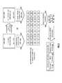
- FIG. 8is a diagram of an example of the memory management module accessing a configured main memory.
- the examplebegins with the memory management module receiving at least one logical address that is associated with a virtual page of addresses 110 .
- the virtual page 110may have a logical address range of 0001 1000 to 0001 1FFF (hexadecimal) (e.g., a 4K word page) and the received logical address is within this range.
- the memory management module 12accesses a logical address to memory module table to identify one or more memory modules of the main memory.
- the tableis graphically represented 114 as a plurality of memory modules arranged in a particular configuration to comprise the main memory.
- a memory module 14stores less than a full page of information (e.g., data and/or instructions). As such, the storage of the virtual page is spread among four memory modules 14 . This may result because the number of cells of the memory modules is less than the page size (e.g., 1K word of memory cells vs. 4K word page size) or because only a portion of the memory cells of memory module are used for a given page and other memory cells are used for other pages.
- the memory management module 12accesses a logical address to physical address table to map the logical address to a physical address and to correspondingly map the virtual page of addresses 110 to a main memory page of addresses 112 .
- the logical addresses of 0001 1000 to 0001 1FFFis mapped to 00F1 1000 to 00F1 1FFF.
- the memory management module 12then accesses a memory module to physical address table to identify one or more memory modules corresponding to the page of main memory.
- the tableis graphically represented 114 as a plurality of memory modules arranged in a particular configuration to comprise the main memory.
- the memory management module 12determines the MMW wireless communication resources to convey the memory access message to the memory modules, the resources for the memory modules to transceive data and/or instructions with the processing module, and/or resources for the memory module to transceive data with the secondary memory module. Once the resources are identified, the memory management module 12 generates a memory module address message 116 that is conveyed to the memory modules 14 via the allocated MMW wireless communication resource.
- the memory module address message 116may include a plurality of fields.
- the message 116may include one or more fields 118 for identifying the memory modules being addressed; one or more fields 120 for the allocated MMW wireless communication resources; and one or more fields 122 for the memory access message or a portion thereof.
- the message 116may further include one or more fields 124 for a local address of the memory modules, which is used when a portion of the memory cells of the memory module are used for a given page and other memory cells are used for other pages. For example, when the memory module stores only one page, or a portion of a page, it can be addressed by its ID. However, when the memory modules stores, is capable of storing, or configured to storing more than just one page, or portion thereof, then the appropriate columns of the memory module need to be individually addressed, or addressed as local group.
- FIG. 9is a diagram of another example of the memory management module accessing a configured main memory.
- the examplebegins with the memory management module receiving at least one logical address that is associated with a virtual page of addresses 110 .
- the virtual page 110may have a logical address range of 0001 1000 to 0001 1FFF (hexadecimal) (e.g., a 4K word page) and the received logical address is within this range.
- the memory management module 12accesses a logical address to memory module table to identify one or more memory modules of the main memory.
- the tableis graphically represented 114 as a plurality of memory modules arranged in a particular configuration to comprise the main memory.
- a memory module 14stores a full page of information (e.g., data and/or instructions).
- the memory management module 12accesses a logical address to physical address table to map the logical address to a physical address and to correspondingly map the virtual page of addresses 110 to a main memory page of addresses 112 .
- the logical addresses of 0001 1000 to 0001 1FFFis mapped to 00F1 1000 to 00F1 1FFF.
- the memory management module 12then accesses a memory module to physical address table to identify the memory modules corresponding to the page of main memory.
- the tableis graphically represented 114 as a plurality of memory modules arranged in a particular configuration to comprise the main memory.
- the memory management module 12determines the MMW wireless communication resources to convey the memory access message to the memory modules, the resources for the memory modules to transceive data and/or instructions with the processing module, and/or resources for the memory module to transceive data with the secondary memory module. Once the resources are identified, the memory management module 12 generates a memory module address message 116 that is conveyed to the memory modules 14 via the allocated MMW wireless communication resource.
- the memory module address message 116may include a plurality of fields.
- the message 116may include one or more fields 118 for identifying the memory modules being addressed; one or more fields 120 for the allocated MMW wireless communication resources; and one or more fields 122 for the memory access message or a portion thereof.
- FIG. 10is a schematic block diagram of an embodiment of a memory management module 12 that includes the memory management unit 86 and the MMW transceiver 88 .
- the MMW transceiver 88includes a baseband processing module 130 and a MMW front-end (FE) 132 .
- the MMW FE 132includes a transmitter section and a receiver section, embodiments of which have been previously discussed.
- the memory management unit 86 and the baseband processing module 130may be implemented via the same processing device or via separate processing devices.
- Such a processing devicemay be a microprocessor, micro-controller, digital signal processor, microcomputer, central processing unit, field programmable gate array, programmable logic device, state machine, logic circuitry, analog circuitry, digital circuitry, and/or any device that manipulates signals (analog and/or digital) based on hard coding of the circuitry and/or operational instructions.
- the processing devicemay have an associated memory and/or memory element, which may be a single memory device, a plurality of memory devices, and/or embedded circuitry of the processing device.
- Such a memory devicemay be a read-only memory, random access memory, volatile memory, non-volatile memory, static memory, dynamic memory, flash memory, cache memory, and/or any device that stores digital information.
- the memory and/or memory element storing the corresponding operational instructionsmay be embedded within, or external to, the circuitry comprising the state machine, analog circuitry, digital circuitry, and/or logic circuitry.
- the memory management module 86receives, or identifies, a virtual page of addresses 110 , processes them to identify main memory page of addresses 112 , and generates a memory module address message 116 .
- the baseband processing module 130converts the memory module address message 116 into an outbound address message symbol stream in a manner as previously discussed.
- the MMW FE 132converts the outbound address message symbol stream into a MMW signal 134 in accordance with the at least one MMW communication resource (e.g., within the appropriate slot(s) and/or on the appropriate channel(s)).
- the MMW FE 132then transmits the MMW signal 134 to the at least one memory module via the at least one MMW communication resource.
- FIG. 11is a schematic block diagram of an embodiment of a memory management module 12 that includes the memory management unit 86 and the MMW transceiver 88 .
- the MMW transceiver 88includes a baseband processing module 130 and a MMW front-end (FE) 132 .
- the memory management unit 86 and the MMW transceiver 88function as previously described to generate the MMW signal 134 .
- the MMW front-end (FE) 132receives an inbound MMW memory access signal 140 from a processing module or other component.
- the MMW FE 132converts the inbound MMW memory access signal 140 into an inbound memory access symbol stream and provides it to the baseband processing module 130 .
- the baseband processing module 130converts the inbound memory access symbol stream into the memory access request 142 , which is conveyed to the memory management unit, which it processes as previously discussed.
- FIG. 12is a schematic block diagram of another embodiment of a circuit 145 that includes the processing module 30 , the memory management module 12 , the secondary memory 42 and the main memory 40 .
- the processing module 30includes a processing core 72 , a processing cache memory 74 (e.g., a data cache and/or an instruction cache), and a millimeter wave (MMW) transceiver 89 .
- the memory management module 12includes the memory management unit 86 and a MMW transceiver (XCVR) 88 .
- the secondary memory module 42includes secondary memory (e.g., a hard disk, flash memory, etc.) and a MMW transceiver 94 .
- the main memory 40includes the plurality of memory modules 14 , which can be configured in a variety as ways as discussed with reference to FIGS. 3 and 4 , and one or more I/O modules 20 .
- the processing core 72may include one or more processing devices such as, but not limited to, a microprocessor, micro-controller, digital signal processor, microcomputer, central processing unit, field programmable gate array, programmable logic device, state machine, logic circuitry, analog circuitry, digital circuitry, and/or any device that manipulates signals [analog and/or digital] based on hard coding of the circuitry and/or operational instructions.
- a processing core 72desires access to the main memory 40 , it generates a memory access request (e.g., a read command, a write command, etc.) that includes a logical address, which it provides to the memory management unit 86 , which may be done via a wired connection or a wireless communication.
- the memory management unit 86determines whether the memory access request can be satisfied by the currently configured main memory 40 (i.e., the requested data and/or instruction is currently stored in main memory 40 ). If yes, the memory management unit 86 identifies the memory module(s) 14 within the main memory that satisfy the memory access request (e.g., is/are identified via the logical to physical address table 36 and the physical address to memory module table 50 or the logical address to memory module table).
- the MMW transceiver 88converts the memory access request into a MMW signal and transmits it to the I/O module 20 via an address wireless communication resource (resource_addr).
- the I/O module 20may function as a repeater and provide the MMW signal to the identified memory module(s) 14 via communication resources within the memory device 10 .
- the I/O module 20may convert the MMW signal into an inbound symbol stream by the MMW FE 24 .
- the baseband unit 22processes the inbound symbol stream to produce an outbound symbol stream.
- the MMW FE 24converts the outbound symbol stream into an intra-device MMW signal that is transmitted to the identified memory module(s) 14 .
- the identified memory module(s) 14recover the memory access request from the intra-device MMW signal and perform the request.
- the memory module(s)reads data (e.g., one or more lines of data, typically a page) from the corresponding memory lines and converts it into an intra-device memory MMW signal, which is transmitted to the MMW front end 24 of the I/O module 20 via one or more wireless communication resources.
- the I/O module 20processes the intra-device memory MMW signal into a MMW signal that is transmitted to the MMW transceiver 89 of the processing module.
- data and/or instructions stored in the cache 74is converted into a write MMW signal that is transmitted to the I/O module 20 via the MMW transceiver and corresponding inter-device wireless communication resources.
- the I/O module 20processes the write MMW signal to produce an intra-device write MMW signal that it provides to the identified memory module(s) 14 , which recovers and performs the corresponding write function.
- the memory management unit 86If the memory access request cannot be satisfied by the currently configured main memory 40 (i.e., the requested data and/or instruction is not currently stored in main memory 40 ), the memory management unit 86 generates a swap message that is converted into one or more MMW signals by MMW transceiver 88 .
- the swap MMW signalis transmitted to the secondary memory module 42 via a secondary memory wireless communication resource and the swap MMW signal is transmitted to the I/O module 20 of the main memory 40 via the address wireless communication resource.
- the MMW transceiver 94recovers the swap message and provides it to the second memory 92 .
- the secondary memory 92reads a page of data and provides it to the MMW transceiver 94 .
- the MMW transceiver 94converts the page of data into a MMW signal that is transmitted to the main memory via a memory transfer wireless communication resource (resource_mem xfr).
- the main memory 40retrieves and sends a page of data (or instructions) to the secondary memory 42 via the memory exchange wireless communication resource.
- the MMW transceiver 94recovers the data and provides it to the secondary memory 92 for storage. Once the desired data (or instruction) is stored in the main memory 40 , it provides the data (or instruction) to the processing module 30 via one or more of the allocated wireless communication resources.
- FIG. 13is a schematic block diagram of another embodiment of a circuit 145 that includes the processing module 30 , the memory management module 12 , the secondary memory 42 and the main memory 40 .
- the processing module 30includes a processing core 72 , a plurality of processing cache memory 74 (e.g., a data cache and/or an instruction cache), and a plurality of millimeter wave (MMW) transceivers 89 .
- the memory management module 12includes the memory management unit 86 and one or more MMW transceivers (XCVR) 88 & 90 .
- the secondary memory module 42includes secondary memory (e.g., a hard disk, flash memory, etc.) and a MMW transceiver 94 .
- the main memory 40includes the plurality of memory modules 14 , which can be configured in a variety as ways as discussed with reference to FIGS. 3 and 4 .
- the processing core 72When the processing core 72 desires access to the main memory 40 , it generates a memory access request (e.g., a read command, a write command, etc.) that includes a logical address, which it provides to the memory management unit 86 , which may be done via a wired connection or a wireless communication.
- the memory management unit 86determines whether the memory access request can be satisfied by the currently configured main memory 40 (i.e., the requested data and/or instruction is currently stored in main memory 40 ). If yes, the memory management unit 86 identifies the memory module(s) 14 within the main memory that satisfy the memory access request (e.g., is/are identified via the logical to physical address table 36 and the physical address to memory module table 50 or the logical address to memory module table).
- the MMW transceiver 88converts the memory access request into a MMW signal and transmits it to the identified memory modules 14 via an address wireless communication resource (resource_addr).
- the identified memory module(s) 14recover the memory access request from the intra-device MMW signal and perform the request.
- the memory module(s)reads data (e.g., one or more lines of data, typically a page) from the corresponding memory lines and converts it into a memory MMW signal, which is transmitted to the MMW transceiver 89 associated with one of the plurality of cache memories 74 via one or more wireless communication resources.
- data and/or instructions stored in the cache 74is converted into a write MMW signal that is transmitted to the identified memory module ( 14 ) via the MMW transceiver 89 and allocated wireless communication resources.
- the identified memory module(s) 14recovers and performs the corresponding write function.
- the memory management unit 86If the memory access request cannot be satisfied by the currently configured main memory 40 (i.e., the requested data and/or instruction is not currently stored in main memory 40 ), the memory management unit 86 generates a swap message that is converted into one or more MMW signals by MMW transceiver 88 and/or 90 .
- the swap MMW signalis transmitted to the secondary memory module 42 via a secondary memory wireless communication resource and the swap MMW signal is transmitted to the main memory 40 via the address wireless communication resource.
- the MMW transceiver 94 of the secondary memory module 42recovers the swap message and provides it to the second memory 92 .
- the secondary memory 92reads a page of data and provides it to the MMW transceiver 94 .
- the MMW transceiver 94converts the page of data into a MMW signal that is transmitted to the main memory via a memory transfer wireless communication resource (resource_mem xfr).
- the main memory 40retrieves and sends a page of data (or instructions) to the secondary memory 42 via the memory exchange wireless communication resource.
- the MMW transceiver 94recovers the data and provides it to the secondary memory 92 for storage. Once the desired data (or instruction) is stored in the main memory 40 , it provides the data (or instruction) to the processing module 30 via one or more of the allocated wireless communication resources.
- a plurality of memory access requestsmay be processed concurrently.
- each cache memory 74may be concurrently active in a memory access request (e.g., read, write, swap, etc.) with negligible interference from the other cache memories' processing of their memory access requests.
- a memory access requeste.g., read, write, swap, etc.
- 32 MMW transceivers 89in the processing module 30
- 32 different and concurrent memory access requests between the processing module 30 and the main memory 40can be supported.
- each memory access requestmay be processes as previously described with respect to a single memory access request.
- FIG. 14is a schematic block diagram of an embodiment of a memory management module 12 wirelessly communicating with a memory module 14 .
- Each module 12 and 14performs a plurality of steps to wirelessly communicate with the other module, with the processing module 30 , and/or with the secondary memory module 42 .
- the memory management module 12performs steps 150 - 162 and the memory module 14 performs steps 166 - 172 .
- the module 12receives a memory access request that includes a logical address, which has been previously discussed.
- the methodcontinues at step 152 where the memory management module 12 determines whether one or more of the plurality of memory modules satisfies the memory access request based on the logical address and a table of logical address to memory modules.
- the tablemay include a mapping of logical addresses to memory module IDs or a first table that maps the logic address to a physical address and another table that maps the physical address to memory module IDs. Satisfying the request was previously discussed.
- the methodproceeds to step 154 where the memory management module 12 generates a memory module message identifying the one or more of the plurality of memory modules and at least a portion of the memory access request.
- the memory management module 12may interpret the memory access request to identify a page of memory based on the logical address. The memory management module 12 may then determine whether the page is stored in the one of the plurality of memory modules or in the one and at least one other memory module of the plurality of memory modules (i.e., is the page completely stored in one memory module or in more than one memory module).
- the memory management module 12determines whether at least part of another page is stored in the one of the plurality of memory modules (e.g., the page size is less than the size of the memory module or the memory module has been configured to store more than one page, or a portion thereof). When at least part of another page is not stored in the memory module, the memory management module generates the memory module message to include an identification code of the memory module. An example of this was provided with reference to FIG. 9 . If, however, at least part of another page is stored in the memory module, the memory management unit 12 generates the memory module message to include the identification code of the one of the plurality of memory modules and a local address. An example of this was provided with reference to FIG. 8 .
- Another example of the memory management module 12 generating the memory module messagebegins with the module 12 determining that the page is stored in multiple memory modules and determining whether at least part of another page is stored in at least one of the multiple memory modules. When at least part of another page is not stored in one or more of the multiple memory modules (e.g., each memory module only stores, is capable of storing, or is configured to store one page, or a portion thereof), the memory management module 12 generates the memory module message to include an identification code of the each of the multiple memory modules.
- the memory management module 12When at least part of another page is stored in the one of the multiple memory modules, the memory management module 12 generates the memory module message to include the identification code of each of the multiple memory modules, a first corresponding local address for one of the multiple memory modules, and a second corresponding local address for a second one of the multiple memory modules.
- the module 12converts the memory module message into a millimeter wave (MMW) memory signal 158 in accordance with a memory module addressing communication resource.
- the memory management module 12then transmits the MMW memory signal 158 to the one or more memory modules via the memory module addressing communication resource.
- MMWmillimeter wave
- the methodcontinues at step 160 where the memory management module 12 generates a swap message.
- the methodthen continues at step 162 where the memory management module converts the swap message into a MMW swap message 164 that it subsequently transmits.
- the module 14begins it method by receiving the MMW memory signal 158 via the memory module addressing communication resource.
- the methodcontinues at step 166 where the memory module 14 recovers the memory module message from the MMW memory signal 158 .
- the methodcontinues at step 168 where the memory module 14 processes at least a portion of the memory access request.
- the methodcontinues at step 170 where the memory module 14 generates a memory access response when required (e.g., a response to a read request).
- the methodthen continues at step 172 where the memory module 14 converts the memory access response into a MMW memory response signal 174 in accordance with a wireless communication resource.
- the memory module 14transmits the MMW memory signal 174 to the processing module 30 or other device.
- FIG. 15is a schematic block diagram of an embodiment of a memory module 14 wirelessly communicating with a secondary memory module 42 .
- Each module 14 and 42performs a plurality of steps to wirelessly communicate with the other module, with the processing module 30 , and/or with the memory management module 12 .
- the memory module 14performs steps 174 - 178 and 194 - 196 and the secondary memory module 42 performs steps 182 - 184 and 186 - 190 .
- the module 14converts the MMW swap message 164 into the swap message.
- the methodcontinues at step 176 where the module 14 processes the swap message to retrieve data stored therein (e.g., all data stored in the memory module or a portion thereof).
- the methodcontinues at step 178 where the memory module 14 converts the retrieved data into a MMW data signal 180 and transmits it to the secondary memory module 42 .
- processingbegins at step 182 where it receives the MMW data signal 180 and recaptures the retrieved data therefrom.
- the methodcontinues at step 182 where the secondary memory module 42 stores the retrieved data at a designated location.
- the secondary memory module 42converts, at step 186 , the MMW swap message 164 into the swap message.
- the processingcontinues at step 188 where the secondary memory module 42 processes the swap message to retrieve second data stored within a second designated location to produce second retrieved data.
- the processingcontinues at step 190 where the secondary memory module 42 converts the second retrieved data into a second MMW data signal 192 and transmits it to the addressed one or more memory modules 14 .
- the methodcontinues with the addressed one or more memory modules 14 at step 194 where the module 14 receives the second MMW data signal 192 and recaptures the second retrieved data therefrom.
- the methodcontinues at step 196 where the memory module 14 stores the second retrieved data.
- the terms “substantially” and “approximately”provides an industry-accepted tolerance for its corresponding term and/or relativity between items. Such an industry-accepted tolerance ranges from less than one percent to fifty percent and corresponds to, but is not limited to, component values, integrated circuit process variations, temperature variations, rise and fall times, and/or thermal noise. Such relativity between items ranges from a difference of a few percent to magnitude differences.
- the term(s) “coupled to” and/or “coupling” and/orincludes direct coupling between items and/or indirect coupling between items via an intervening item (e.g., an item includes, but is not limited to, a component, an element, a circuit, and/or a module) where, for indirect coupling, the intervening item does not modify the information of a signal but may adjust its current level, voltage level, and/or power level.
- an intervening iteme.g., an item includes, but is not limited to, a component, an element, a circuit, and/or a module
- inferred couplingi.e., where one element is coupled to another element by inference
- the term “operable to”indicates that an item includes one or more of power connections, input(s), output(s), etc., to perform one or more its corresponding functions and may further include inferred coupling to one or more other items.
- the term “associated with”,includes direct and/or indirect coupling of separate items and/or one item being embedded within another item.
- the term “compares favorably”,indicates that a comparison between two or more items, signals, etc., provides a desired relationship. For example, when the desired relationship is that signal 1 has a greater magnitude than signal 2 , a favorable comparison may be achieved when the magnitude of signal 1 is greater than that of signal 2 or when the magnitude of signal 2 is less than that of signal 1 .
Landscapes
- Engineering & Computer Science (AREA)
- Theoretical Computer Science (AREA)
- Physics & Mathematics (AREA)
- General Engineering & Computer Science (AREA)
- General Physics & Mathematics (AREA)
- Memory System (AREA)
- Mobile Radio Communication Systems (AREA)
Abstract
Description
Claims (22)
Priority Applications (2)
| Application Number | Priority Date | Filing Date | Title |
|---|---|---|---|
| US12/236,294US8239650B2 (en) | 2007-01-31 | 2008-09-23 | Wirelessly configurable memory device addressing |
| US13/542,284US8661224B2 (en) | 2007-01-31 | 2012-07-05 | Wirelessly configurable memory device addressing |
Applications Claiming Priority (5)
| Application Number | Priority Date | Filing Date | Title |
|---|---|---|---|
| US11/700,285US8116294B2 (en) | 2007-01-31 | 2007-01-31 | RF bus controller |
| US11/888,068US8010735B2 (en) | 2007-07-31 | 2007-07-31 | Flash memory with millimeter wave host interface and method for use therewith |
| US12/026,681US20090197641A1 (en) | 2008-02-06 | 2008-02-06 | Computing device with handheld and extended computing units |
| US12/202,260US8175108B2 (en) | 2007-01-31 | 2008-08-30 | Wirelessly configurable memory device |
| US12/236,294US8239650B2 (en) | 2007-01-31 | 2008-09-23 | Wirelessly configurable memory device addressing |
Related Parent Applications (1)
| Application Number | Title | Priority Date | Filing Date |
|---|---|---|---|
| US12/026,681Continuation-In-PartUS20090197641A1 (en) | 2007-01-31 | 2008-02-06 | Computing device with handheld and extended computing units |
Related Child Applications (1)
| Application Number | Title | Priority Date | Filing Date |
|---|---|---|---|
| US13/542,284ContinuationUS8661224B2 (en) | 2007-01-31 | 2012-07-05 | Wirelessly configurable memory device addressing |
Publications (2)
| Publication Number | Publication Date |
|---|---|
| US20090019250A1 US20090019250A1 (en) | 2009-01-15 |
| US8239650B2true US8239650B2 (en) | 2012-08-07 |
Family
ID=40254097
Family Applications (2)
| Application Number | Title | Priority Date | Filing Date |
|---|---|---|---|
| US12/236,294Expired - Fee RelatedUS8239650B2 (en) | 2007-01-31 | 2008-09-23 | Wirelessly configurable memory device addressing |
| US13/542,284Expired - Fee RelatedUS8661224B2 (en) | 2007-01-31 | 2012-07-05 | Wirelessly configurable memory device addressing |
Family Applications After (1)
| Application Number | Title | Priority Date | Filing Date |
|---|---|---|---|
| US13/542,284Expired - Fee RelatedUS8661224B2 (en) | 2007-01-31 | 2012-07-05 | Wirelessly configurable memory device addressing |
Country Status (1)
| Country | Link |
|---|---|
| US (2) | US8239650B2 (en) |
Families Citing this family (14)
| Publication number | Priority date | Publication date | Assignee | Title |
|---|---|---|---|---|
| US8510560B1 (en) | 2008-08-20 | 2013-08-13 | Marvell International Ltd. | Efficient key establishment for wireless networks |
| WO2010033497A1 (en) | 2008-09-18 | 2010-03-25 | Marvell World Trade Ltd. | Preloading applications onto memory at least partially during boot up |
| US20100180182A1 (en)* | 2009-01-09 | 2010-07-15 | Seagate Technology Llc | Data memory device and controller with interface error detection and handling logic |
| US20130082767A1 (en)* | 2011-09-29 | 2013-04-04 | Broadcom Corporation | Signal distribution and radiation in a wireless enabled integrated circuit (ic) |
| US9075105B2 (en) | 2011-09-29 | 2015-07-07 | Broadcom Corporation | Passive probing of various locations in a wireless enabled integrated circuit (IC) |
| US9318785B2 (en) | 2011-09-29 | 2016-04-19 | Broadcom Corporation | Apparatus for reconfiguring an integrated waveguide |
| US9570420B2 (en) | 2011-09-29 | 2017-02-14 | Broadcom Corporation | Wireless communicating among vertically arranged integrated circuits (ICs) in a semiconductor package |
| US9736801B1 (en) | 2013-05-20 | 2017-08-15 | Marvell International Ltd. | Methods and apparatus for synchronizing devices in a wireless data communication system |
| US9521635B1 (en) | 2013-05-21 | 2016-12-13 | Marvell International Ltd. | Methods and apparatus for selecting a device to perform shared functionality in a deterministic and fair manner in a wireless data communication system |
| WO2015038568A1 (en)* | 2013-09-10 | 2015-03-19 | Marvell World Trade Ltd. | Secure device bootstrap identity |
| CA2951050A1 (en)* | 2014-06-04 | 2015-12-10 | Csa Medical, Inc. | Method and system for consistent, repeatable, and safe cryospray treatment of airway tissue |
| US20150363329A1 (en)* | 2014-06-12 | 2015-12-17 | Hamilton Sundstrand Corporation | Memory address translation |
| US10979412B2 (en) | 2016-03-08 | 2021-04-13 | Nxp Usa, Inc. | Methods and apparatus for secure device authentication |
| CN107632944B (en)* | 2017-09-22 | 2021-06-18 | 郑州云海信息技术有限公司 | A method and device for reading data |
Citations (100)
| Publication number | Priority date | Publication date | Assignee | Title |
|---|---|---|---|---|
| US4807183A (en) | 1985-09-27 | 1989-02-21 | Carnegie-Mellon University | Programmable interconnection chip for computer system functional modules |
| US5502683A (en) | 1993-04-20 | 1996-03-26 | International Business Machines Corporation | Dual ported memory with word line access control |
| US5754948A (en) | 1995-12-29 | 1998-05-19 | University Of North Carolina At Charlotte | Millimeter-wave wireless interconnection of electronic components |
| US5786912A (en) | 1996-12-27 | 1998-07-28 | Lucent Technologies Inc. | Waveguide-based, fabricless switch for telecommunication system and telecommunication infrastructure employing the same |
| US5809321A (en) | 1995-08-16 | 1998-09-15 | Microunity Systems Engineering, Inc. | General purpose, multiple precision parallel operation, programmable media processor |
| US5884104A (en) | 1997-11-26 | 1999-03-16 | Eastman Kodak Company | Compact camera flash unit |
| US6182203B1 (en) | 1997-01-24 | 2001-01-30 | Texas Instruments Incorporated | Microprocessor |
| US6234900B1 (en) | 1997-08-22 | 2001-05-22 | Blake Cumbers | Player tracking and identification system |
| US20020022521A1 (en) | 2000-05-15 | 2002-02-21 | Konami Corporation | Game machine and network system for setting up game environment thereof |
| US20020049806A1 (en) | 2000-05-16 | 2002-04-25 | Scott Gatz | Parental control system for use in connection with account-based internet access server |
| US20020061012A1 (en) | 1999-04-13 | 2002-05-23 | Thi James C. | Cable modem with voice processing capability |
| US20020107010A1 (en) | 2000-12-22 | 2002-08-08 | Witte Markus Valter | Communication system for use with a vehicle |
| US6438622B1 (en) | 1998-11-17 | 2002-08-20 | Intel Corporation | Multiprocessor system including a docking system |
| US20020164945A1 (en) | 2001-05-02 | 2002-11-07 | Olsen Randall B. | Narrow beamwidth communication link with alignment camera |
| US6500070B1 (en) | 1999-05-28 | 2002-12-31 | Nintendo Co., Ltd. | Combined game system of portable and video game machines |
| US20030001882A1 (en) | 2001-06-29 | 2003-01-02 | Macer Peter J. | Portable entertainment machines |
| US6505305B1 (en)* | 1998-07-16 | 2003-01-07 | Compaq Information Technologies Group, L.P. | Fail-over of multiple memory blocks in multiple memory modules in computer system |
| US20030017845A1 (en) | 1995-06-01 | 2003-01-23 | Padcom, Inc. | Apparatus and method for intelligent routing of data between a remote device and a host system |
| US20030023828A1 (en)* | 2000-09-15 | 2003-01-30 | March Roger W. | Memory devices and methods for use therewith |
| US20030040284A1 (en) | 2000-12-05 | 2003-02-27 | Masanori Sato | Method and apparatus of retransmitted data combination |
| US20030059022A1 (en) | 2001-09-24 | 2003-03-27 | Nebiker Robert M. | Multi-media communication downloading |
| US20030078071A1 (en) | 2001-10-22 | 2003-04-24 | Koji Uchiyama | Cordless and wireless telephone docking station with land line interface and switching mode |
| US20030112585A1 (en) | 2001-12-13 | 2003-06-19 | Silvester Kelan Craig | Multiprocessor notebook computer with a tablet PC conversion capability |
| US20030126335A1 (en) | 1999-12-23 | 2003-07-03 | Kelan C. Silvester | Notebook computer with independently functional, dockable core computer |
| US20030128712A1 (en) | 2002-01-09 | 2003-07-10 | Norihiko Moriwaki | Packet communication apparatus and controlling method thereof |
| US20030162503A1 (en) | 2002-02-26 | 2003-08-28 | Motorola, Inc. | Dynamic reallocation of processing resources for redundant functionality |
| US20030172380A1 (en) | 2001-06-05 | 2003-09-11 | Dan Kikinis | Audio command and response for IPGs |
| US20030221036A1 (en) | 2002-05-24 | 2003-11-27 | Dell Products, L.P. | Information handling system featuring multi-processor capability with processor located in docking station |
| US6663295B2 (en) | 2001-01-26 | 2003-12-16 | Nec Corporation | Optical transmitter-receiver module suitable for reducing crosstalk |
| US20040054776A1 (en) | 2002-09-16 | 2004-03-18 | Finisar Corporation | Network expert analysis process |
| US20040062308A1 (en) | 2002-09-27 | 2004-04-01 | Kamosa Gregg Mark | System and method for accelerating video data processing |
| US6735708B2 (en) | 1999-10-08 | 2004-05-11 | Dell Usa, L.P. | Apparatus and method for a combination personal digital assistant and network portable device |
| US6735663B2 (en) | 2000-12-18 | 2004-05-11 | Dell Products L.P. | Combination personal data assistant and personal computing device |
| US20040117442A1 (en) | 2002-12-10 | 2004-06-17 | Thielen Kurt R. | Handheld portable wireless digital content player |
| US20040123113A1 (en) | 2002-12-18 | 2004-06-24 | Svein Mathiassen | Portable or embedded access and input devices and methods for giving access to access limited devices, apparatuses, appliances, systems or networks |
| US20040153863A1 (en) | 2002-09-16 | 2004-08-05 | Finisar Corporation | Network analysis omniscent loop state machine |
| US20040157559A1 (en) | 2003-02-10 | 2004-08-12 | Kabushiki Kaisha Toshiba | Information providing apparatus, information receiver, information providing program, information receiving program and wireless communication apparatus |
| US20040174431A1 (en) | 2001-05-14 | 2004-09-09 | Stienstra Marcelle Andrea | Device for interacting with real-time streams of content |
| US6801974B1 (en) | 2001-01-26 | 2004-10-05 | Dell Products L.P. | Method of filtering events in a combinational computing device |
| US20040203364A1 (en) | 2002-05-23 | 2004-10-14 | Silvester Kelan C. | Method and apparatus for dynamically resolving radio frequency interference problems in a system |
| US6816925B2 (en) | 2001-01-26 | 2004-11-09 | Dell Products L.P. | Combination personal data assistant and personal computing device with master slave input output |
| US20040266336A1 (en) | 2003-04-25 | 2004-12-30 | Stelios Patsiokas | System and method for providing recording and playback of digital media content |
| EP1499070A2 (en) | 2003-07-18 | 2005-01-19 | Nokia Corporation | Integration of a plurality of short-range communication protocols |
| US20050060598A1 (en) | 2003-09-12 | 2005-03-17 | Finisar Corporation | Network analysis tool |
| US20050124307A1 (en) | 2003-12-08 | 2005-06-09 | Xytrans, Inc. | Low cost broadband wireless communication system |
| US20050185364A1 (en) | 2004-01-05 | 2005-08-25 | Jory Bell | Docking station for mobile computing device |
| US20050250531A1 (en) | 2004-05-10 | 2005-11-10 | Kabushiki Kaisha Toshiba | Mobile communication terminal having plurality of operation modes |
| US20060026348A1 (en) | 2004-07-08 | 2006-02-02 | Wallace Robert F | Portable memory devices with removable caps that effect operation of the devices when attached |
| US20060038731A1 (en) | 2004-08-18 | 2006-02-23 | Microsoft Corporation | Parallel loop antennas for a mobile electronic device |
| US20060046762A1 (en) | 2004-08-27 | 2006-03-02 | Samsung Electronics Co., Ltd. | System and method for controlling congestion between response messages responsive to a group call page in a mobile communication system |
| US20060085675A1 (en) | 2004-10-12 | 2006-04-20 | Andrew Popell | One-touch backup system |
| US20060101164A1 (en) | 2000-06-12 | 2006-05-11 | Broadcom Corporation | Context switch architecture and system |
| US7065326B2 (en) | 2001-05-02 | 2006-06-20 | Trex Enterprises Corporation | Millimeter wave communications system with a high performance modulator circuit |
| US20060148568A1 (en) | 2004-12-30 | 2006-07-06 | Motorola, Inc. | Device and method for wirelessly accessing game media |
| US7082285B2 (en) | 2001-03-23 | 2006-07-25 | Broadcom Corporation | Reduced instruction set baseband controller |
| US20060167784A1 (en) | 2004-09-10 | 2006-07-27 | Hoffberg Steven M | Game theoretic prioritization scheme for mobile ad hoc networks permitting hierarchal deference |
| US20060164271A1 (en) | 2003-03-12 | 2006-07-27 | Walter Hirt | Method and apparatus for converting optical signals to radio channels |
| US20060176851A1 (en) | 2005-02-07 | 2006-08-10 | Bennett James D | Computer chip set having on board wireless interfaces to support test operations |
| US20060190691A1 (en) | 2005-02-03 | 2006-08-24 | Nicolas Chauve | Die-to-die interconnect interface and protocol for stacked semiconductor dies |
| US20060203758A1 (en) | 2005-03-11 | 2006-09-14 | Samsung Electronics Co., Ltd. | Mobile terminal for relaying multimedia data to an external display device |
| US20060252470A1 (en) | 2005-05-03 | 2006-11-09 | Nambirajan Seshadri | Modular ear-piece/microphone (headset) operable to service voice activated commands |
| US20060262026A1 (en) | 2005-05-18 | 2006-11-23 | Widefi, Inc. | Integrated, closely spaced, high isolation, printed dipoles |
| US20060260546A1 (en) | 2003-08-28 | 2006-11-23 | Hitachi, Ltd. | Semiconductor device and its manufacturing method |
| US20060269004A1 (en) | 2005-05-26 | 2006-11-30 | Brima Ibrahim | Method and system for digital spur cancellation |
| US20060282635A1 (en) | 2005-06-10 | 2006-12-14 | Mather Clifford J | Apparatus and method for configuring memory blocks |
| US7159099B2 (en) | 2002-06-28 | 2007-01-02 | Motorola, Inc. | Streaming vector processor with reconfigurable interconnection switch |
| US20070015558A1 (en) | 2002-07-27 | 2007-01-18 | Sony Computer Entertainment America Inc. | Method and apparatus for use in determining an activity level of a user in relation to a system |
| US7171050B2 (en) | 2002-03-19 | 2007-01-30 | Samsung Electronics Co., Ltd. | System on chip processor for multimedia devices |
| US20070038808A1 (en) | 2005-07-13 | 2007-02-15 | Samsung Electronics Co., Ltd. | Data storage system with complex memory and method of operating the same |
| US7197584B2 (en) | 2001-01-26 | 2007-03-27 | Dell Products L.P. | Removable personal digital assistant in a dual personal computer/personal digital assistant computer architecture |
| US7218143B1 (en) | 2005-06-14 | 2007-05-15 | Xilinx, Inc. | Integrated circuit having fast interconnect paths between memory elements and carry logic |
| US20070147152A1 (en) | 2002-11-08 | 2007-06-28 | Hitachi, Ltd. | Sense amplifier for semiconductor memory device |
| US20070155502A1 (en) | 2005-12-16 | 2007-07-05 | Pixart Imaging Inc. | Device for motion tracking and object for reflecting infrared light |
| US20070167149A1 (en) | 2001-05-31 | 2007-07-19 | Palm, Inc. | System and method for communicating with a network access node |
| US7257093B1 (en) | 2001-10-10 | 2007-08-14 | Sandia Corporation | Localized radio frequency communication using asynchronous transfer mode protocol |
| US20070229270A1 (en) | 2006-03-16 | 2007-10-04 | Broadcom Corporation, A California Corporation | RFID system with RF bus |
| US20070239929A1 (en) | 2006-04-07 | 2007-10-11 | Chen Ben W | Wireless flash memory card expansion system |
| US20070268481A1 (en) | 2006-05-17 | 2007-11-22 | Ramesh Raskar | System and method for measuring scene reflectance using optical sensors |
| US20070298882A1 (en) | 2003-09-15 | 2007-12-27 | Sony Computer Entertainment Inc. | Methods and systems for enabling direction detection when interfacing with a computer program |
| US20080020843A1 (en) | 2002-05-13 | 2008-01-24 | New Illuminations Llc | Method and apparatus using insertably-removable auxiliary devices to play games over a communications link |
| US20080028118A1 (en) | 2006-07-31 | 2008-01-31 | Craig Peter Sayers | Portable dock for a portable computing system |
| US7330702B2 (en) | 2005-01-31 | 2008-02-12 | Taiwan Semiconductor Manufacturing Co., Ltd. | Method and apparatus for inter-chip wireless communication |
| US20080040541A1 (en) | 2004-09-22 | 2008-02-14 | Mark Brockmann | System and Method for Configuring Memory Devices for Use in a Network |
| US20080063236A1 (en) | 2006-06-09 | 2008-03-13 | Sony Computer Entertainment Inc. | Object Tracker for Visually Tracking Object Motion |
| US20080070516A1 (en) | 2006-09-15 | 2008-03-20 | Plantronics, Inc. | Audio data streaming with auto switching between wireless headset and speakers |
| US20080076406A1 (en) | 2006-09-22 | 2008-03-27 | Vanu, Inc. | Wireless Backhaul |
| US20080151847A1 (en) | 2006-12-22 | 2008-06-26 | Canon Kabushiki Kaisha | Automated wireless access to peripheral devices |
| US7406062B2 (en) | 2004-02-10 | 2008-07-29 | Realtek Semiconductor Corp. | Method for selecting a channel in a wireless network |
| US20080244148A1 (en) | 2007-04-02 | 2008-10-02 | Go2Call.Com, Inc. | VoIP Enabled Femtocell with a USB Transceiver Station |
| US7444393B2 (en) | 2001-10-30 | 2008-10-28 | Keicy K. Chung | Read-only storage device having network interface, a system including the device, and a method of distributing files over a network |
| WO2009002464A2 (en) | 2007-06-22 | 2008-12-31 | Vubiq Incorporated | System and method for wireless communication in a backplane fabric architecture |
| US20090006640A1 (en) | 2007-06-28 | 2009-01-01 | Michael Lambertus Hubertus Brouwer | Incremental secure backup and restore of user settings and data |
| US20090198854A1 (en) | 2008-02-06 | 2009-08-06 | Broadcom Corporation | File storage for a computing device with handheld and extended computing units |
| US20090215533A1 (en) | 2008-02-27 | 2009-08-27 | Gary Zalewski | Methods for capturing depth data of a scene and applying computer actions |
| US20100056132A1 (en) | 2008-08-29 | 2010-03-04 | Mark Gallagher | System and method for femtocell management |
| US20100120447A1 (en) | 2008-11-11 | 2010-05-13 | Trueposition, Inc. | Femto-Cell Location by Direct Methods |
| US20100146199A1 (en) | 2005-09-26 | 2010-06-10 | Rambus Inc. | Memory System Topologies Including A Buffer Device And An Integrated Circuit Memory Device |
| US20100273468A1 (en) | 2009-04-28 | 2010-10-28 | Maik Bienas | Methods and apparatus for configuration of femtocells in a wireless network |
| US7903724B2 (en) | 2007-01-31 | 2011-03-08 | Broadcom Corporation | RF transceiver device with RF bus |
| US20110134868A1 (en) | 2008-08-04 | 2011-06-09 | Moon Il Lee | Method and apparatus of transmitting data in multiple rf system |
- 2008
- 2008-09-23USUS12/236,294patent/US8239650B2/ennot_activeExpired - Fee Related
- 2012
- 2012-07-05USUS13/542,284patent/US8661224B2/ennot_activeExpired - Fee Related
Patent Citations (103)
| Publication number | Priority date | Publication date | Assignee | Title |
|---|---|---|---|---|
| US4807183A (en) | 1985-09-27 | 1989-02-21 | Carnegie-Mellon University | Programmable interconnection chip for computer system functional modules |
| US5502683A (en) | 1993-04-20 | 1996-03-26 | International Business Machines Corporation | Dual ported memory with word line access control |
| US20030017845A1 (en) | 1995-06-01 | 2003-01-23 | Padcom, Inc. | Apparatus and method for intelligent routing of data between a remote device and a host system |
| US5809321A (en) | 1995-08-16 | 1998-09-15 | Microunity Systems Engineering, Inc. | General purpose, multiple precision parallel operation, programmable media processor |
| US5754948A (en) | 1995-12-29 | 1998-05-19 | University Of North Carolina At Charlotte | Millimeter-wave wireless interconnection of electronic components |
| US5786912A (en) | 1996-12-27 | 1998-07-28 | Lucent Technologies Inc. | Waveguide-based, fabricless switch for telecommunication system and telecommunication infrastructure employing the same |
| US6182203B1 (en) | 1997-01-24 | 2001-01-30 | Texas Instruments Incorporated | Microprocessor |
| US6234900B1 (en) | 1997-08-22 | 2001-05-22 | Blake Cumbers | Player tracking and identification system |
| US5884104A (en) | 1997-11-26 | 1999-03-16 | Eastman Kodak Company | Compact camera flash unit |
| US6505305B1 (en)* | 1998-07-16 | 2003-01-07 | Compaq Information Technologies Group, L.P. | Fail-over of multiple memory blocks in multiple memory modules in computer system |
| US6438622B1 (en) | 1998-11-17 | 2002-08-20 | Intel Corporation | Multiprocessor system including a docking system |
| US20020061012A1 (en) | 1999-04-13 | 2002-05-23 | Thi James C. | Cable modem with voice processing capability |
| US6500070B1 (en) | 1999-05-28 | 2002-12-31 | Nintendo Co., Ltd. | Combined game system of portable and video game machines |
| US6735708B2 (en) | 1999-10-08 | 2004-05-11 | Dell Usa, L.P. | Apparatus and method for a combination personal digital assistant and network portable device |
| US20030126335A1 (en) | 1999-12-23 | 2003-07-03 | Kelan C. Silvester | Notebook computer with independently functional, dockable core computer |
| US20020022521A1 (en) | 2000-05-15 | 2002-02-21 | Konami Corporation | Game machine and network system for setting up game environment thereof |
| US20020049806A1 (en) | 2000-05-16 | 2002-04-25 | Scott Gatz | Parental control system for use in connection with account-based internet access server |
| US20060101164A1 (en) | 2000-06-12 | 2006-05-11 | Broadcom Corporation | Context switch architecture and system |
| US20030023828A1 (en)* | 2000-09-15 | 2003-01-30 | March Roger W. | Memory devices and methods for use therewith |
| US20030040284A1 (en) | 2000-12-05 | 2003-02-27 | Masanori Sato | Method and apparatus of retransmitted data combination |
| US7149837B2 (en) | 2000-12-18 | 2006-12-12 | Dell Products L.P. | Method of operating combination personal data assistant and personal computing device |
| US6735663B2 (en) | 2000-12-18 | 2004-05-11 | Dell Products L.P. | Combination personal data assistant and personal computing device |
| US20020107010A1 (en) | 2000-12-22 | 2002-08-08 | Witte Markus Valter | Communication system for use with a vehicle |
| US6801974B1 (en) | 2001-01-26 | 2004-10-05 | Dell Products L.P. | Method of filtering events in a combinational computing device |
| US6816925B2 (en) | 2001-01-26 | 2004-11-09 | Dell Products L.P. | Combination personal data assistant and personal computing device with master slave input output |
| US6663295B2 (en) | 2001-01-26 | 2003-12-16 | Nec Corporation | Optical transmitter-receiver module suitable for reducing crosstalk |
| US7197584B2 (en) | 2001-01-26 | 2007-03-27 | Dell Products L.P. | Removable personal digital assistant in a dual personal computer/personal digital assistant computer architecture |
| US7082285B2 (en) | 2001-03-23 | 2006-07-25 | Broadcom Corporation | Reduced instruction set baseband controller |
| US20020164945A1 (en) | 2001-05-02 | 2002-11-07 | Olsen Randall B. | Narrow beamwidth communication link with alignment camera |
| US7065326B2 (en) | 2001-05-02 | 2006-06-20 | Trex Enterprises Corporation | Millimeter wave communications system with a high performance modulator circuit |
| US20040174431A1 (en) | 2001-05-14 | 2004-09-09 | Stienstra Marcelle Andrea | Device for interacting with real-time streams of content |
| US20070167149A1 (en) | 2001-05-31 | 2007-07-19 | Palm, Inc. | System and method for communicating with a network access node |
| US20030172380A1 (en) | 2001-06-05 | 2003-09-11 | Dan Kikinis | Audio command and response for IPGs |
| US20030001882A1 (en) | 2001-06-29 | 2003-01-02 | Macer Peter J. | Portable entertainment machines |
| US20030059022A1 (en) | 2001-09-24 | 2003-03-27 | Nebiker Robert M. | Multi-media communication downloading |
| US7257093B1 (en) | 2001-10-10 | 2007-08-14 | Sandia Corporation | Localized radio frequency communication using asynchronous transfer mode protocol |
| US20030078071A1 (en) | 2001-10-22 | 2003-04-24 | Koji Uchiyama | Cordless and wireless telephone docking station with land line interface and switching mode |
| US7444393B2 (en) | 2001-10-30 | 2008-10-28 | Keicy K. Chung | Read-only storage device having network interface, a system including the device, and a method of distributing files over a network |
| US20030112585A1 (en) | 2001-12-13 | 2003-06-19 | Silvester Kelan Craig | Multiprocessor notebook computer with a tablet PC conversion capability |
| US20030128712A1 (en) | 2002-01-09 | 2003-07-10 | Norihiko Moriwaki | Packet communication apparatus and controlling method thereof |
| US20030162503A1 (en) | 2002-02-26 | 2003-08-28 | Motorola, Inc. | Dynamic reallocation of processing resources for redundant functionality |
| US7171050B2 (en) | 2002-03-19 | 2007-01-30 | Samsung Electronics Co., Ltd. | System on chip processor for multimedia devices |
| US20080020843A1 (en) | 2002-05-13 | 2008-01-24 | New Illuminations Llc | Method and apparatus using insertably-removable auxiliary devices to play games over a communications link |
| US20040203364A1 (en) | 2002-05-23 | 2004-10-14 | Silvester Kelan C. | Method and apparatus for dynamically resolving radio frequency interference problems in a system |
| US20030221036A1 (en) | 2002-05-24 | 2003-11-27 | Dell Products, L.P. | Information handling system featuring multi-processor capability with processor located in docking station |
| US7159099B2 (en) | 2002-06-28 | 2007-01-02 | Motorola, Inc. | Streaming vector processor with reconfigurable interconnection switch |
| US20070015558A1 (en) | 2002-07-27 | 2007-01-18 | Sony Computer Entertainment America Inc. | Method and apparatus for use in determining an activity level of a user in relation to a system |
| US20040153863A1 (en) | 2002-09-16 | 2004-08-05 | Finisar Corporation | Network analysis omniscent loop state machine |
| US20040054776A1 (en) | 2002-09-16 | 2004-03-18 | Finisar Corporation | Network expert analysis process |
| US20040062308A1 (en) | 2002-09-27 | 2004-04-01 | Kamosa Gregg Mark | System and method for accelerating video data processing |
| US20070147152A1 (en) | 2002-11-08 | 2007-06-28 | Hitachi, Ltd. | Sense amplifier for semiconductor memory device |
| US20040117442A1 (en) | 2002-12-10 | 2004-06-17 | Thielen Kurt R. | Handheld portable wireless digital content player |
| US20040123113A1 (en) | 2002-12-18 | 2004-06-24 | Svein Mathiassen | Portable or embedded access and input devices and methods for giving access to access limited devices, apparatuses, appliances, systems or networks |
| US20040157559A1 (en) | 2003-02-10 | 2004-08-12 | Kabushiki Kaisha Toshiba | Information providing apparatus, information receiver, information providing program, information receiving program and wireless communication apparatus |
| US20060164271A1 (en) | 2003-03-12 | 2006-07-27 | Walter Hirt | Method and apparatus for converting optical signals to radio channels |
| US20040266336A1 (en) | 2003-04-25 | 2004-12-30 | Stelios Patsiokas | System and method for providing recording and playback of digital media content |
| US20050014468A1 (en) | 2003-07-18 | 2005-01-20 | Juha Salokannel | Scalable bluetooth multi-mode radio module |
| EP1499070A2 (en) | 2003-07-18 | 2005-01-19 | Nokia Corporation | Integration of a plurality of short-range communication protocols |
| US20060260546A1 (en) | 2003-08-28 | 2006-11-23 | Hitachi, Ltd. | Semiconductor device and its manufacturing method |
| US20050060598A1 (en) | 2003-09-12 | 2005-03-17 | Finisar Corporation | Network analysis tool |
| US20070298882A1 (en) | 2003-09-15 | 2007-12-27 | Sony Computer Entertainment Inc. | Methods and systems for enabling direction detection when interfacing with a computer program |
| US20050124307A1 (en) | 2003-12-08 | 2005-06-09 | Xytrans, Inc. | Low cost broadband wireless communication system |
| US20050185364A1 (en) | 2004-01-05 | 2005-08-25 | Jory Bell | Docking station for mobile computing device |
| US7406062B2 (en) | 2004-02-10 | 2008-07-29 | Realtek Semiconductor Corp. | Method for selecting a channel in a wireless network |
| US20050250531A1 (en) | 2004-05-10 | 2005-11-10 | Kabushiki Kaisha Toshiba | Mobile communication terminal having plurality of operation modes |
| US20060026348A1 (en) | 2004-07-08 | 2006-02-02 | Wallace Robert F | Portable memory devices with removable caps that effect operation of the devices when attached |
| US20060038731A1 (en) | 2004-08-18 | 2006-02-23 | Microsoft Corporation | Parallel loop antennas for a mobile electronic device |
| US20060046762A1 (en) | 2004-08-27 | 2006-03-02 | Samsung Electronics Co., Ltd. | System and method for controlling congestion between response messages responsive to a group call page in a mobile communication system |
| US20060167784A1 (en) | 2004-09-10 | 2006-07-27 | Hoffberg Steven M | Game theoretic prioritization scheme for mobile ad hoc networks permitting hierarchal deference |
| US20080040541A1 (en) | 2004-09-22 | 2008-02-14 | Mark Brockmann | System and Method for Configuring Memory Devices for Use in a Network |
| US20060085675A1 (en) | 2004-10-12 | 2006-04-20 | Andrew Popell | One-touch backup system |
| US20060148568A1 (en) | 2004-12-30 | 2006-07-06 | Motorola, Inc. | Device and method for wirelessly accessing game media |
| US7330702B2 (en) | 2005-01-31 | 2008-02-12 | Taiwan Semiconductor Manufacturing Co., Ltd. | Method and apparatus for inter-chip wireless communication |
| US20060190691A1 (en) | 2005-02-03 | 2006-08-24 | Nicolas Chauve | Die-to-die interconnect interface and protocol for stacked semiconductor dies |
| US20060176851A1 (en) | 2005-02-07 | 2006-08-10 | Bennett James D | Computer chip set having on board wireless interfaces to support test operations |
| US20060203758A1 (en) | 2005-03-11 | 2006-09-14 | Samsung Electronics Co., Ltd. | Mobile terminal for relaying multimedia data to an external display device |
| US20060252470A1 (en) | 2005-05-03 | 2006-11-09 | Nambirajan Seshadri | Modular ear-piece/microphone (headset) operable to service voice activated commands |
| US20060262026A1 (en) | 2005-05-18 | 2006-11-23 | Widefi, Inc. | Integrated, closely spaced, high isolation, printed dipoles |
| US20060269004A1 (en) | 2005-05-26 | 2006-11-30 | Brima Ibrahim | Method and system for digital spur cancellation |
| US20060282635A1 (en) | 2005-06-10 | 2006-12-14 | Mather Clifford J | Apparatus and method for configuring memory blocks |
| US7218143B1 (en) | 2005-06-14 | 2007-05-15 | Xilinx, Inc. | Integrated circuit having fast interconnect paths between memory elements and carry logic |
| US20070038808A1 (en) | 2005-07-13 | 2007-02-15 | Samsung Electronics Co., Ltd. | Data storage system with complex memory and method of operating the same |
| US20100146199A1 (en) | 2005-09-26 | 2010-06-10 | Rambus Inc. | Memory System Topologies Including A Buffer Device And An Integrated Circuit Memory Device |
| US20070155502A1 (en) | 2005-12-16 | 2007-07-05 | Pixart Imaging Inc. | Device for motion tracking and object for reflecting infrared light |
| US20070229270A1 (en) | 2006-03-16 | 2007-10-04 | Broadcom Corporation, A California Corporation | RFID system with RF bus |
| US20070239929A1 (en) | 2006-04-07 | 2007-10-11 | Chen Ben W | Wireless flash memory card expansion system |
| US20070268481A1 (en) | 2006-05-17 | 2007-11-22 | Ramesh Raskar | System and method for measuring scene reflectance using optical sensors |
| US20080063236A1 (en) | 2006-06-09 | 2008-03-13 | Sony Computer Entertainment Inc. | Object Tracker for Visually Tracking Object Motion |
| US20080028118A1 (en) | 2006-07-31 | 2008-01-31 | Craig Peter Sayers | Portable dock for a portable computing system |
| US20080070516A1 (en) | 2006-09-15 | 2008-03-20 | Plantronics, Inc. | Audio data streaming with auto switching between wireless headset and speakers |
| US20080076406A1 (en) | 2006-09-22 | 2008-03-27 | Vanu, Inc. | Wireless Backhaul |
| US20080151847A1 (en) | 2006-12-22 | 2008-06-26 | Canon Kabushiki Kaisha | Automated wireless access to peripheral devices |
| US7903724B2 (en) | 2007-01-31 | 2011-03-08 | Broadcom Corporation | RF transceiver device with RF bus |
| US20080244148A1 (en) | 2007-04-02 | 2008-10-02 | Go2Call.Com, Inc. | VoIP Enabled Femtocell with a USB Transceiver Station |
| WO2009002464A2 (en) | 2007-06-22 | 2008-12-31 | Vubiq Incorporated | System and method for wireless communication in a backplane fabric architecture |
| US7929474B2 (en) | 2007-06-22 | 2011-04-19 | Vubiq Incorporated | System and method for wireless communication in a backplane fabric architecture |
| US20090006640A1 (en) | 2007-06-28 | 2009-01-01 | Michael Lambertus Hubertus Brouwer | Incremental secure backup and restore of user settings and data |
| US20090198854A1 (en) | 2008-02-06 | 2009-08-06 | Broadcom Corporation | File storage for a computing device with handheld and extended computing units |
| US20090215533A1 (en) | 2008-02-27 | 2009-08-27 | Gary Zalewski | Methods for capturing depth data of a scene and applying computer actions |
| US20110134868A1 (en) | 2008-08-04 | 2011-06-09 | Moon Il Lee | Method and apparatus of transmitting data in multiple rf system |
| US20100056132A1 (en) | 2008-08-29 | 2010-03-04 | Mark Gallagher | System and method for femtocell management |
| US20100120447A1 (en) | 2008-11-11 | 2010-05-13 | Trueposition, Inc. | Femto-Cell Location by Direct Methods |
| US20100273468A1 (en) | 2009-04-28 | 2010-10-28 | Maik Bienas | Methods and apparatus for configuration of femtocells in a wireless network |
Non-Patent Citations (9)
| Title |
|---|
| Bruce K Gale, "RF, Electrical, and Magnetic Microsystems," date unknown, 8 pages, Apr. 18, 2003. |
| Dr. Lynn Fuller, "Microelectromechanical Systems (MEMs) Applications-Microphones,"Rochester Institute of Technology Microelectronic Engineering, Apr. 25, 2005, pp. 1-43. |
| Dr. Lynn Fuller, "Microelectromechanical Systems (MEMs) Applications—Microphones,"Rochester Institute of Technology Microelectronic Engineering, Apr. 25, 2005, pp. 1-43. |
| E3 Wii Controller; Nintendo Wilmote; Technology Limitations; Xgaming, Inc.; pp. 1-5, May 28, 2005. |
| Elsadek, et al.; "A Compact 3-D Microwave Holographic Pointer System Using a Size Reduced Microstrip Planar Array"; Department of Electrical and Computer Engineering; University of California; pp. 1-5, Aug. 6, 2002. |
| Elsadek, et al.; "Microstrip Multi-element Diversity Antenna Array for Three Dimensional Microwave Holographic Input Pointer (Holo3D)"; Department of Electrical and Computer Engineering; University of California; pp. 1-4, Aug. 7, 2002. |
| Haworth, et al.; Public Security Screening for Metallic Objects with Millimetre-Wave Images; Heriot-Watt University; United Kingdom; pp. 1-4, Oct. 10, 2005. |
| Radio Control Adapter; IBM Technical Disclosure Bulletin NN86081337; IBM; Aug. 1986. |
| Xilinx Inc.: Spartan-3AN FPGA Family Data Sheet, DS557, Jun. 2, 2008, p. 5. |
Also Published As
| Publication number | Publication date |
|---|---|
| US20090019250A1 (en) | 2009-01-15 |
| US20120284481A1 (en) | 2012-11-08 |
| US8661224B2 (en) | 2014-02-25 |
Similar Documents
| Publication | Publication Date | Title |
|---|---|---|
| US8239650B2 (en) | Wirelessly configurable memory device addressing | |
| US8621175B2 (en) | Wirelessly configurable memory device | |
| US20250258601A1 (en) | Apparatus and method to share host system ram with mass storage memory ram | |
| US12355853B2 (en) | Memory system allowing host to easily transmit and receive data | |
| CN101091189B (en) | Combined IC card and wireless transceiver module for mobile communication equipment | |
| JP5313301B2 (en) | Wireless internet access device, SD control chip, and data communication method | |
| US20090037627A1 (en) | Flash memory with millimeter wave host interface and method for use therewith | |
| US20080046638A1 (en) | Multiprocessor System having an Input/Output (I/O) Bridge Circuit for Transferring Data Between Volatile and Non-Volatile Memory | |
| JP2616455B2 (en) | Wireless modem | |
| JPWO2004077306A1 (en) | SDIO controller | |
| EP3893119B1 (en) | System on chip, routing method for access command and terminal | |
| US20060253673A1 (en) | Apparatus and method for permitting access to storage means | |
| CN100538678C (en) | High-speed internal wireless bus | |
| US20090037670A1 (en) | Disk controller with millimeter wave host interface and method for use therewith | |
| US8238275B2 (en) | IC with MMW transceiver communications | |
| US9128811B2 (en) | Assigning addresses to devices on an interconnect | |
| CN203366744U (en) | Wireless USB flash disk device supporting self-building of hot spot | |
| US20090022215A1 (en) | Modem | |
| US20110053634A1 (en) | Handheld communication devices with shared processing and methods for use therewith | |
| CN114238160B (en) | Address access method, device and electronic device | |
| CN117931465A (en) | Data transmission method and related device | |
| CN117971710B (en) | Method and device for dynamic multiplexing of memory, electronic equipment and storage medium | |
| US20250117345A1 (en) | Method for communicating data between a slave device and a master device, and corresponding integrated system | |
| CN117135281A (en) | Communication device, telephone card switching method, and computer-readable storage medium | |
| CN114499592A (en) | System and method for reducing NFC power consumption and improving reliability |
Legal Events
| Date | Code | Title | Description |
|---|---|---|---|
| AS | Assignment | Owner name:BROADCOM CORPORATION, CALIFORNIA Free format text:ASSIGNMENT OF ASSIGNORS INTEREST;ASSIGNORS:ROFOUGARAN, AHMADREZA (REZA);MARKISON, TIMOTHY W.;REEL/FRAME:021588/0444 Effective date:20080923 | |
| FEPP | Fee payment procedure | Free format text:PAYOR NUMBER ASSIGNED (ORIGINAL EVENT CODE: ASPN); ENTITY STATUS OF PATENT OWNER: LARGE ENTITY | |
| AS | Assignment | Owner name:BANK OF AMERICA, N.A., AS COLLATERAL AGENT, NORTH CAROLINA Free format text:PATENT SECURITY AGREEMENT;ASSIGNOR:BROADCOM CORPORATION;REEL/FRAME:037806/0001 Effective date:20160201 Owner name:BANK OF AMERICA, N.A., AS COLLATERAL AGENT, NORTH Free format text:PATENT SECURITY AGREEMENT;ASSIGNOR:BROADCOM CORPORATION;REEL/FRAME:037806/0001 Effective date:20160201 | |
| REMI | Maintenance fee reminder mailed | ||
| LAPS | Lapse for failure to pay maintenance fees | ||
| STCH | Information on status: patent discontinuation | Free format text:PATENT EXPIRED DUE TO NONPAYMENT OF MAINTENANCE FEES UNDER 37 CFR 1.362 | |
| FP | Lapsed due to failure to pay maintenance fee | Effective date:20160807 | |
| AS | Assignment | Owner name:AVAGO TECHNOLOGIES GENERAL IP (SINGAPORE) PTE. LTD., SINGAPORE Free format text:ASSIGNMENT OF ASSIGNORS INTEREST;ASSIGNOR:BROADCOM CORPORATION;REEL/FRAME:041706/0001 Effective date:20170120 Owner name:AVAGO TECHNOLOGIES GENERAL IP (SINGAPORE) PTE. LTD Free format text:ASSIGNMENT OF ASSIGNORS INTEREST;ASSIGNOR:BROADCOM CORPORATION;REEL/FRAME:041706/0001 Effective date:20170120 | |
| AS | Assignment | Owner name:BROADCOM CORPORATION, CALIFORNIA Free format text:TERMINATION AND RELEASE OF SECURITY INTEREST IN PATENTS;ASSIGNOR:BANK OF AMERICA, N.A., AS COLLATERAL AGENT;REEL/FRAME:041712/0001 Effective date:20170119 |