US8239607B2 - System and method for an asynchronous data buffer having buffer write and read pointers - Google Patents
System and method for an asynchronous data buffer having buffer write and read pointersDownload PDFInfo
- Publication number
- US8239607B2 US8239607B2US12/553,856US55385609AUS8239607B2US 8239607 B2US8239607 B2US 8239607B2US 55385609 AUS55385609 AUS 55385609AUS 8239607 B2US8239607 B2US 8239607B2
- Authority
- US
- United States
- Prior art keywords
- coupled
- flip
- data
- flops
- pointer
- Prior art date
- Legal status (The legal status is an assumption and is not a legal conclusion. Google has not performed a legal analysis and makes no representation as to the accuracy of the status listed.)
- Expired - Lifetime
Links
Images


Classifications
- G—PHYSICS
- G06—COMPUTING OR CALCULATING; COUNTING
- G06F—ELECTRIC DIGITAL DATA PROCESSING
- G06F13/00—Interconnection of, or transfer of information or other signals between, memories, input/output devices or central processing units
- G06F13/14—Handling requests for interconnection or transfer
- G06F13/16—Handling requests for interconnection or transfer for access to memory bus
- G06F13/1668—Details of memory controller
- G06F13/1689—Synchronisation and timing concerns
- G—PHYSICS
- G06—COMPUTING OR CALCULATING; COUNTING
- G06F—ELECTRIC DIGITAL DATA PROCESSING
- G06F13/00—Interconnection of, or transfer of information or other signals between, memories, input/output devices or central processing units
- G06F13/14—Handling requests for interconnection or transfer
- G06F13/16—Handling requests for interconnection or transfer for access to memory bus
- G06F13/1668—Details of memory controller
- G06F13/1684—Details of memory controller using multiple buses
- G—PHYSICS
- G11—INFORMATION STORAGE
- G11C—STATIC STORES
- G11C29/00—Checking stores for correct operation ; Subsequent repair; Testing stores during standby or offline operation
- G11C29/02—Detection or location of defective auxiliary circuits, e.g. defective refresh counters
- G—PHYSICS
- G11—INFORMATION STORAGE
- G11C—STATIC STORES
- G11C29/00—Checking stores for correct operation ; Subsequent repair; Testing stores during standby or offline operation
- G11C29/02—Detection or location of defective auxiliary circuits, e.g. defective refresh counters
- G11C29/022—Detection or location of defective auxiliary circuits, e.g. defective refresh counters in I/O circuitry
- G—PHYSICS
- G11—INFORMATION STORAGE
- G11C—STATIC STORES
- G11C29/00—Checking stores for correct operation ; Subsequent repair; Testing stores during standby or offline operation
- G11C29/02—Detection or location of defective auxiliary circuits, e.g. defective refresh counters
- G11C29/023—Detection or location of defective auxiliary circuits, e.g. defective refresh counters in clock generator or timing circuitry
- G—PHYSICS
- G11—INFORMATION STORAGE
- G11C—STATIC STORES
- G11C29/00—Checking stores for correct operation ; Subsequent repair; Testing stores during standby or offline operation
- G11C29/02—Detection or location of defective auxiliary circuits, e.g. defective refresh counters
- G11C29/025—Detection or location of defective auxiliary circuits, e.g. defective refresh counters in signal lines
- G—PHYSICS
- G11—INFORMATION STORAGE
- G11C—STATIC STORES
- G11C29/00—Checking stores for correct operation ; Subsequent repair; Testing stores during standby or offline operation
- G11C29/02—Detection or location of defective auxiliary circuits, e.g. defective refresh counters
- G11C29/028—Detection or location of defective auxiliary circuits, e.g. defective refresh counters with adaption or trimming of parameters
- G—PHYSICS
- G11—INFORMATION STORAGE
- G11C—STATIC STORES
- G11C29/00—Checking stores for correct operation ; Subsequent repair; Testing stores during standby or offline operation
- G11C29/04—Detection or location of defective memory elements, e.g. cell constructio details, timing of test signals
- G11C29/50—Marginal testing, e.g. race, voltage or current testing
- G11C29/50012—Marginal testing, e.g. race, voltage or current testing of timing
- G—PHYSICS
- G11—INFORMATION STORAGE
- G11C—STATIC STORES
- G11C7/00—Arrangements for writing information into, or reading information out from, a digital store
- G11C7/10—Input/output [I/O] data interface arrangements, e.g. I/O data control circuits, I/O data buffers
- G11C7/1006—Data managing, e.g. manipulating data before writing or reading out, data bus switches or control circuits therefor
- G11C7/1012—Data reordering during input/output, e.g. crossbars, layers of multiplexers, shifting or rotating
- G—PHYSICS
- G11—INFORMATION STORAGE
- G11C—STATIC STORES
- G11C7/00—Arrangements for writing information into, or reading information out from, a digital store
- G11C7/10—Input/output [I/O] data interface arrangements, e.g. I/O data control circuits, I/O data buffers
- G11C7/1015—Read-write modes for single port memories, i.e. having either a random port or a serial port
- G11C7/1039—Read-write modes for single port memories, i.e. having either a random port or a serial port using pipelining techniques, i.e. using latches between functional memory parts, e.g. row/column decoders, I/O buffers, sense amplifiers
- G—PHYSICS
- G11—INFORMATION STORAGE
- G11C—STATIC STORES
- G11C7/00—Arrangements for writing information into, or reading information out from, a digital store
- G11C7/10—Input/output [I/O] data interface arrangements, e.g. I/O data control circuits, I/O data buffers
- G11C7/1051—Data output circuits, e.g. read-out amplifiers, data output buffers, data output registers, data output level conversion circuits
- G11C7/1066—Output synchronization
- G—PHYSICS
- G11—INFORMATION STORAGE
- G11C—STATIC STORES
- G11C7/00—Arrangements for writing information into, or reading information out from, a digital store
- G11C7/10—Input/output [I/O] data interface arrangements, e.g. I/O data control circuits, I/O data buffers
- G11C7/1051—Data output circuits, e.g. read-out amplifiers, data output buffers, data output registers, data output level conversion circuits
- G11C7/1069—I/O lines read out arrangements
- G—PHYSICS
- G11—INFORMATION STORAGE
- G11C—STATIC STORES
- G11C7/00—Arrangements for writing information into, or reading information out from, a digital store
- G11C7/10—Input/output [I/O] data interface arrangements, e.g. I/O data control circuits, I/O data buffers
- G11C7/1078—Data input circuits, e.g. write amplifiers, data input buffers, data input registers, data input level conversion circuits
- G11C7/1093—Input synchronization
- G—PHYSICS
- G11—INFORMATION STORAGE
- G11C—STATIC STORES
- G11C7/00—Arrangements for writing information into, or reading information out from, a digital store
- G11C7/22—Read-write [R-W] timing or clocking circuits; Read-write [R-W] control signal generators or management
- G—PHYSICS
- G11—INFORMATION STORAGE
- G11C—STATIC STORES
- G11C5/00—Details of stores covered by group G11C11/00
- G11C5/02—Disposition of storage elements, e.g. in the form of a matrix array
- G11C5/04—Supports for storage elements, e.g. memory modules; Mounting or fixing of storage elements on such supports
Definitions
- the present inventionis related generally to a memory system for a processor-based system, and more particularly, to synchronizing the coupling of read data across different clock domains and providing information related to the timing margin in crossing the different clock domains.
- Computer systemsuse memory devices, such as dynamic random access memory (“DRAM”) devices, to store data that are accessed by a processor. These memory devices are normally used as system memory in a computer system.
- the processorcommunicates with the system memory through a processor bus and a memory controller.
- the memory devices of the system memorytypically arranged in memory modules having multiple memory devices, are coupled through a memory bus to the memory controller.
- the processorissues a memory request, which includes a memory command, such as a read command, and an address designating the location from which data or instructions are to be read.
- the memory controlleruses the command and address to generate appropriate command signals as well as row and column addresses, which are applied to the system memory through the memory bus.
- dataare transferred between the system memory and the processor.
- the memory controlleris often part of a system controller, which also includes bus bridge circuitry for coupling the processor bus to an expansion bus, such as a PCI bus.
- bandwidth limitationsare not related to the memory controllers since the memory controllers sequence data to and from the system memory as fast as the memory devices allow.
- One approach that has been taken to increase bandwidthis to increase the speed of the memory data bus coupling the memory controller to the memory devices.
- the same amount of informationcan be moved over the memory data bus in less time.
- a corresponding increase in bandwidthdoes not result.
- One reason for the non-linear relationship between data bus speed and bandwidthis the hardware limitations within the memory devices themselves. That is, the memory controller has to schedule all memory commands to the memory devices such that the hardware limitations are honored.
- the performance of computer systemsis also limited by latency problems that increase the time required to read data from system memory devices. More specifically, when a memory device read command is coupled to a system memory device, such as a synchronous DRAM (“SDRAM”) device, the read data are output from the SDRAM device only after a delay of several clock periods. Therefore, although SDRAM devices can synchronously output burst data at a high data rate, the delay in initially providing the data can significantly slow the operating speed of a computer system using such SDRAM devices. Increasing the memory data bus speed can be used to help alleviate the latency issue. However, as with bandwidth, the increase in memory data bus speeds do not yield a linear reduction of latency, for essentially the same reasons previously discussed.
- SDRAMsynchronous DRAM
- a computer system 100 shown in FIG. 1uses a memory hub architecture.
- the computer system 100includes a processor 104 for performing various computing functions, such as executing specific software to perform specific calculations or tasks.
- the processor 104includes a processor bus 106 that normally includes an address bus, a control bus, and a data bus.
- the processor bus 106is typically coupled to cache memory 108 , which, is typically static random access memory (“SRAM”).
- SRAMstatic random access memory
- the processor bus 106is coupled to a system controller 110 , which is also sometimes referred to as a bus bridge.
- the system controller 110serves as a communications path to the processor 104 for a variety of other components.
- the system controller 110includes a graphics port that is typically coupled to a graphics controller 112 , which is, in turn, coupled to a video terminal 114 .
- the system controller 110is also coupled to one or more input devices 118 , such as a keyboard or a mouse, to allow an operator to interface with the computer system 100 .
- the computer system 100also includes one or more output devices 120 , such as a printer, coupled to the processor 104 through the system controller 110 .
- One or more data storage devices 124are also typically coupled to the processor 104 through the system controller 110 to allow the processor 104 to store data or retrieve data from internal or external storage media (not shown). Examples of typical storage devices 124 include hard and floppy disks, tape cassettes, and compact disk read-only memories (CD-ROMs).
- the system controller 110includes a memory hub controller 128 that is coupled to the processor 104 .
- the system controller 110is further coupled over a high speed bi-directional or unidirectional system controller/hub interface 134 to several memory modules 130 a - n .
- the controller/hub interface 134includes a downstream bus 154 and an upstream bus 156 which are used to couple data, address, and/or control signals away from or toward, respectively, the memory hub controller 128 .
- the memory modules 130 a - nare coupled in a point-to-point or daisy chain architecture such that the memory modules 130 a - n are connected one to another in series.
- the system controller 110is coupled to a first memory module 130 a , with the first memory module 130 a connected to a second memory module 130 b , and the second memory module 130 b coupled to a third memory module 130 c , and so on in a daisy chain fashion.
- Each memory module 130 a - nincludes a memory hub 140 that is coupled to the system controller/hub interface 134 , and is further coupled a number of memory devices 148 through command, address and data buses, collectively shown as local memory bus 150 .
- the memory hub 140efficiently routes memory requests and responses between the memory hub controller 128 and the memory devices 148 .
- the memory devices 148 on the memory modules 130 a - nare typically capable of operating at high clock frequencies in order to facilitate the relatively high speed operation of the overall memory system. Consequently, computer systems employing this architecture can also use the high-speed system controller/hub interface 134 to complement the high clock speeds of the memory devices 148 . Additionally, with a memory hub based system, signal integrity can be maintained on the system controller/hub interface 134 since the signals are typically transmitted through multiple memory hubs 140 to and from the memory hub controller 128 . Moreover, this architecture also provides for easy expansion of the system memory without concern for degradation in signal quality as more memory modules are added, such as occurs in conventional memory bus architectures.
- the memory hub architecture shown in FIG. 1provides improved memory system performance
- the design of the hub memory system, and more generally, computer systems including such a memory hub architecturebecomes increasingly difficult.
- the processoris coupled through a memory hub controller to each of several memory hubs via a high speed bus or link over which signals, such as command, address, or data signals, are transferred at a very high rate.
- the memory hubsare, in turn, coupled to several memory devices via buses that must also operate at a very high speed.
- transfer ratesincrease, the time for which a signal represents valid information is decreasing.
- the window or “eye” for when the signals are validdecreases at higher transfer rates.
- the “data eye”decreases.
- the data eye for each of the data signalsdefines the actual duration that each signal is valid after various factors affecting the signal are considered, such as timing skew, voltage and current drive capability, and the like.
- timing skew of signalsit often arises from a variety of timing errors such as loading on the lines of the bus, the physical lengths of such lines, and drifting operating conditions.
- One approach to alleviating timing problems in memory devicesis to use a delay-locked loop (DLL) to lock or align the receipt of read data from a memory device and a capture strobe signal used to latch the read data in a memory hub. More specifically, a read strobe signal is output by the memory devices along with read data signals.
- DLLdelay-locked loop
- the timing of when the read strobe signal and the read data are provided by the memory device to a memory hubmay slowly drift in relation to a core clock domain used to synchronize operation of the memory hub and the memory device. The timing may slowly drift due to variations in the operating conditions, such as increasing operating temperature or voltage variations.
- a DLL included in the memory deviceis used to maintain synchronization of the operation of the memory device and the memory controller. This is accomplished by the memory device by aligning its output strobe to an input clock signal that is sourced from the memory controller or provided by a common clock signal sourced to the memory controller and memory device. That is, as the timing between the memory device and memory hub begins to drift, the DLL can adjust the timing of internal clock signals of the memory device relative to the core clock signal thereby “re-synchronizing” operation of the memory device and the memory hub.
- the DLLis thus effective in preventing substantial drifting of the read data strobe and the read data in relation to the core clock domain.
- the timing specifications for the DLLbecome more stringent and therefore increasingly difficult to meet.
- DLL circuitry sufficient to accommodate such timing needsoften consume substantial power as well.
- the amount of circuitry required to implement a suitable DLLcan materially reduce the amount of space that could otherwise be used for memory device circuitry, thereby either increasing the cost or reducing the storage capacity of such memory devices.
- a system for facilitating the adjustment of timing parameters between a memory controller operating in a first clock domain and a memory device operating in a second clock domainmonitors a write pointer and a read pointer to provide a write-read pointer offset representing the timing between when read data is made available by the memory device and when the read data is retrieved by the memory controller. Based on the write-read pointer offset, adjustment to different timing parameters can be made.
- Such a systemcan include a data buffer coupled to the memory device and having a plurality of data locations at which read data are respectively stored and a multiplexer coupled to the data buffer to selectively couple read data stored at respective data locations of the data buffer to an output terminal in accordance with a selection signal.
- a write pointer circuitis coupled to the memory device and the data buffer to generate a write pointer signal to sequentially select one of the plurality of data locations of the data buffer for storing read data received from the memory device responsive to a strobe signal provided by the memory device.
- a read pointer circuitis coupled to the multiplexer to generate responsive to the core clock signal a read pointer signal provided to the multiplexer to sequentially select one of the plurality of data locations of the buffer from which the read data stored therein is coupled to the output terminal of the multiplexer.
- a write-read pointer compare circuitcoupled to the write and read pointer circuits compares the write and read pointer signals to generate a write-read pointer offset signal indicative of the comparison.
- a method of adjusting the relative timing between issuing memory write commands and memory read commandsincludes storing read data provided by at least one memory device in sequentially selected data locations of a buffer, the data location at which read data are currently stored selected by a write pointer.
- the read data stored in the bufferis retrieved from sequentially selected data locations, the data location from which read data are currently retrieved selected by a read pointer.
- a write-read pointer offsetis generated indicative of a data location offset between the data location selected by the write pointer and the data location selected by the read pointer, the timing between the issuance of memory write commands and memory read commands is adjusted based on the write-read pointer offset.
- FIG. 1is a partial block diagram of a computer system having a memory hub based system memory in which embodiments of the present invention can be implemented.
- FIG. 2is a partial block diagram of a memory hub used in the computer system of FIG. 1 , which contains read synchronization modules according to an embodiment of the present invention.
- FIG. 3a partial block diagram of a read synchronization circuit according to an embodiment of the present invention.
- FIG. 4is a partial block diagram of a write pointer circuit according to an embodiment of the present invention that may be substituted into the read synchronization circuit of FIG. 3 .
- FIG. 5is a partial block diagram of a read pointer circuit and a portion of a compare circuit according to embodiments of the present invention that may be substituted into the read synchronization circuit of FIG. 3 .
- FIG. 6is a partial block diagram of another portion of the a compare circuit of FIG. 5 .
- Embodiments of the present inventionare directed to a read data synchronization circuit for coupling read data across two clock domains and providing information on the timing margin between when read data is made available and when the data can be retrieved.
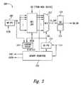
- FIG. 2illustrates a memory hub 200 in which an embodiment of the present invention is implemented.
- the memory hub 200can be substituted for the memory hub 140 of FIG. 1 .
- the memory hub 200is shown in FIG. 2 as being coupled to system memory 240 a - d .
- the system memory 240 a - dis representative of different types of memory devices and different numbers of memory devices.
- each system memory 240 a - drepresents a conventional double data rate (DDR) synchronous dynamic random access memory (SDRAM) device.
- DDRdouble data rate
- SDRAMsynchronous dynamic random access memory
- each of the system memory 240 a - drepresents a bank of memory having a plurality of memory devices. It will be appreciated that the necessary modifications to the memory hub 200 to accommodate the different types and number of memory devices is within the knowledge of those ordinarily skilled in the art, and will not be discussed herein in the interest of brevity.
- link interfaces 210 a , 210 b and 212 a , 212 bfor coupling the memory module on which the memory hub 200 is located to the bus system 134 .
- the link interfaces 210 a , 210 bare coupled to the downstream bus 154 and the link interfaces 212 a , 212 b are coupled to the upstream bus 156 .
- the link interfaces 210 a , 210 b and 212 a , 212 bare conventional, and include conventional circuitry used for transferring data, command, and address information to and from the downstream and upstream busses 154 , 156 .
- the link interfaces 210 a , 210 b and 212 a , 212 bare coupled to a switch 260 through a plurality of bus and signal lines, represented by busses 214 .
- the busses 214are conventional, and include a write data bus and a read data bus, although a single bi-directional data bus may alternatively be provided to couple data through the link interfaces 210 a , 210 b and 212 a , 212 b.
- the switch 260 coupling the link interfaces 210 a - d , 212 a - d and the memory interfaces 270 a - dcan be any of a variety of conventional or hereinafter developed switches.
- the switch 260can be a conventional cross-bar switch that can simultaneously couple link interfaces 210 a , 210 b and 212 a , 212 b and the memory interfaces 270 a - d to each other in a variety of arrangements.
- the switch 260may also include arbitration logic (not shown) to determine which memory accesses should receive priority over other memory accesses. Bus arbitration performing this function is well known to one skilled in the art.
- the switch 260is further coupled to four memory interfaces 270 a - d which are, in turn, coupled to the system memory 240 a - d , respectively.
- the switch 260is coupled to each memory interface through a plurality of bus and signal lines, represented by busses 274 .
- the busses 274include a write data bus, a read data bus, and a request line.
- the memory interfaces 270 a - dare adapted to the system memory 240 a - d to which it is coupled. More specifically, the memory interfaces 270 a - d are specially adapted to provide and receive the specific signals received and generated, respectively, by the system memory 240 a - d to which it is coupled. Also, the memory interfaces 270 a - d are capable of operating with system memory 240 a - d operating at different clock frequencies.
- the memory interfaces 270 a - disolate the processor 104 from changes that may occur at the interface between the memory hub 230 and memory devices 240 a - d coupled to the memory hub 200 , and provide a more controlled environment to which the memory devices 240 a - d may interface.
- each of the memory interfaces 270 a - dincludes a respective memory controller 280 , a respective write buffer 282 , and a respective cache memory unit 284 .
- the memory controller 280performs the same functions as a conventional memory controller by providing control, address and data signals to the system memory device 240 a - d to which it is coupled and receiving data signals from the system memory device 240 a - d to which it is coupled.
- the write buffer 282 and the cache memory unit 284include the normal components of a buffer and cache memory, including a tag memory, a data memory, a comparator, and the like, as is well known in the art.
- the write buffer 282 in each memory interface 270 a - dcan be used to store write requests while a read request is being serviced.
- the cache memory unit 284 in each memory interface 270 a - dallows the processor 104 to receive data responsive to a read command directed to a respective system memory 240 a - d without waiting for the system memory 240 a - d to provide such data in the event that the data was recently read from or written to that memory device 240 a - d.
- Embodiments of the present inventionprovide a read synchronization module 297 for determining timing margin between when read data is provided by the system memory 240 and when the read data is retrieved by the memory controller 280 .
- the read datais provided according to a memory device clock signal and the read data retrieved according to a core clock signal that has a lower frequency than the memory device clock signal.
- various timing parameters between the memory controller 280 and the system memory 240can be adjusted.
- the memory synchronization module 297can be used to synchronize the coupling of read data from the memory device with the core clock domain of the memory hub 200 as established by a system clock signal from the memory hub controller 128 .
- the memory synchronization module 297By having the memory synchronization module 297 adjust for timing drift of the read strobe signal and read data relative to the core clock signal, it may be possible to eliminate DLL circuitry from the memory device since the memory synchronization module 297 tracks when read data is latched by the memory controller 280 and when the read data is available for reading, and if necessary, adjusts the latching and the reading of the data to accommodate for the timing drift.
- a single synchronization module 297is shown in FIG. 2 , it is to be understood that a plurality of synchronization modules 297 may also be used, for example, one per memory controller 280 . Further, in the embodiment shown in FIG. 2 , the synchronization module 297 is shown in communication with the memory device 240 c and the memory controller 280 c . In some embodiments, the synchronization module 297 may be in communication with one or more memory devices and the controller 100 or memory hub 140 shown in FIG. 1 . It will be further appreciated that the read synchronization module 297 may be included as part of the memory controller 280 , although shown in FIG. 2 as a separate functional block.
- FIG. 3illustrates a read data synchronization circuit 300 according to an embodiment of the present invention.
- the read data synchronization circuit 300can be substituted for the read data synchronization circuit 297 shown in FIG. 2 .
- the read data synchronization circuit 300 shown in FIG. 3is operable for one bit of the read data.
- the functional blocks shown in FIG. 3should be generally repeated for every bit of the read data. It will be appreciated, however, that it may not be necessary for some functional blocks to repeated. Those ordinarily skilled in the art will obtain sufficient understanding from the description provided herein in order to practice the present invention.
- the read data synchronization circuit 300provides for coupling read data across two clock domains, namely coupling read data from the system memory 240 operating according to a memory clock signal and the memory hubs 140 operating according to a core clock signal.
- the frequency of the memory clock signalis greater than the frequency of the core clock signal.
- the core clock signalis represented by the CLK signal and the memory clock signal is represented by the RSTB signal.
- the RSTB signalis a read strobe signal that is transmitted by the system memory 240 along with the read data as an indication that read data is being transmitted, as known in the art.
- the RSTB signalis not the actual memory clock signal, the RSTB signal has a timing relative to, and the same frequency as, the memory clock signal.
- the RSTB signalis used to synchronize read data capture.
- the read data synchronization circuit 300includes a data buffer 304 .
- the buffer 304is conventional, and can be configured as a first-in-first-out (FIFO) buffer.
- the buffer 304includes n data locations for storing up to n data.
- the buffer 304is coupled to receive the RSTB signal in order to capture data in response to each clock transition of the RSTB signal.
- the buffer 304is further coupled to a write pointer circuit 308 . In response to the RSTB signal, the write pointer circuit 308 provides an enable signal EN to the buffer 304 to selectively enable one of the n data locations to which memory read data DQ is to be written.
- the write pointer circuit 308disables the current data location and enables a next data location of the FIFO to which the next memory read data DQ is to be written. In this manner, the data locations of the buffer 304 are incremented through in response to each transition of the RSTB signal so that as new memory read data DQ is provided to the buffer 304 , each memory read data DQ is captured at one of the n data locations of the buffer 304 in response to the RSTB signal that is provided with the memory read data DQ.
- the EN signalBy using the EN signal to select which one of the n data locations to write the memory read data DQ, the EN signal provides a “write pointer” that “points” to the data location in the buffer 304 that memory read data DQ is to be written.
- the write pointer circuit 308operates the buffer 304 as a circular buffer in that after n memory read data DQ are written to the n data locations, the n+1 memory read data DQ will overwrite the memory read data DQ written to a first data location of the buffer 304 . Consequently, it is desirable for the memory read data DQ at the first data location to have been retrieved before being overwritten. It will be appreciated that the number of data locations of the buffer 304 should be sufficient to prevent new memory read data DQ written to the buffer 304 according to the memory clock signal from overwriting memory read data DQ already written to the buffer 304 , but not yet retrieved according to a lower frequency core clock signal CLK.
- a multiplexer 312is coupled to the buffer 304 to select m of the n data locations and provide the data stored in the m selected data locations as output data DQ_OUT.
- the output data DQ_OUTis coupled to a latch circuit 314 , which latches the m output data DQ_OUT in response to the rising edge of the core clock signal CLK and provides the data as read data DQ_RD.
- Selection by the multiplexer 312is based on a selection signal SEL provided by a read pointer circuit 316 that is coupled to the multiplexer 312 and the memory controller 280 ( FIG. 2 ).
- the SEL signalis indicative of the data locations of the buffer 304 from which data is selected for provision by the multiplexer 312 as output data DQ_OUT.
- the SEL signalprovides a “read pointer” that “points” to the data locations in the buffer 304 from which data is read.
- the memory controller 280provides memory device command signals CMD and memory address signals ADDR to the system memory 240 .
- the memory sequencerfurther enables the read pointer circuit 316 at a time relative to sending a read command to the system memory 240 in order to select from the buffer 304 m memory read data DQ to be provided as output data DQ_OUT.
- the read pointer circuit 316increments through groups of m data locations of the buffer 304 in response to the core clock signal CLK.
- the multiplexer 312selects m of the n data locations simultaneously in response to the CLK signal to accommodate the higher clock frequency of the memory clock signal relative to the frequency of the CLK signal. It will be appreciated by those ordinarily skilled in the art that the m number of data locations to be selected by the multiplexer 312 will be based on the number of memory read DQ provided by the system memory 280 for every clock cycle of the CLK signal.
- the read data synchronization circuit 300further includes a compare circuit 320 that is coupled to the write pointer circuit 308 and the read pointer circuit 316 .
- the compare circuit 320compares the EN and SEL signals to determine an offset between the data location of the buffer 304 to which memory read data DQ is written and the data locations of the buffer 304 from which data is provided by the multiplexer 312 as output data DQ_OUT. That is, with reference to the previous discussion of write and read pointers, the compare circuit 320 determines the offset between the write pointer and the read pointer.
- a signal OFFSET indicative of the offset between the write and read pointersis generated by the compare circuit 320 and provided to the memory controller 280 .
- the offset between the write and read pointers determined by the compare circuit 318can be used by the memory controller 280 to gauge timing margins, and if appropriate, adjust timing parameters such as to reduce read latency and command turn-around times.
- the read data synchronization circuit 300will be described with respect to a conventional “burst” read operation for a DDR memory device.
- a burst read operation in a DDR memory devicea first data is provided after a time delay from the latching of a column address by the memory device. Thereafter, new data is provided in response to each transition of a memory clock signal applied to the DDR memory device until the burst operation is terminated.
- the DDR memory deviceoutputs data twice, that is, once in response to a rising edge of the memory clock signal and again in response to a falling edge of the memory clock signal.
- the buffer 304 and the multiplexer 312function to de-serialize the memory read data DQ received from the system memory 240 in accordance with the memory device clock signal to be provided in parallel from the multiplexer 312 according to the core clock signal CLK.
- the memory controller 280transmits CMD and ADDR signals to the memory devices 148 in order to execute a burst read operation.
- the write pointer of the write pointer circuit 308 and the read pointer of the read pointer circuit 316are pointing to the same data location of the buffer 304 .
- the system memory 240access the memory cell locations corresponding to the ADDR signals to retrieve the requested read data, and provide the requested read data to the buffer 304 as memory read data DQ. Since the present example is directed to a burst read operation, new memory read data DQ is provided to the buffer 304 in response to each transition of the memory clock signal. As previously discussed, the system memory 240 transmits a RSTB signal with each memory read data DQ provided to the buffer 304 . In the case of a burst read operation, the RSTB signal clocks between two logic levels at the same frequency as the memory clock signal. Consequently, the write pointer circuit 308 sequentially enables data locations in the buffer 304 in response to each transition of the RSTB signal in order to capture the memory read data DQ provided to the buffer 304 in response to each transition of the memory clock signal.
- the memory controller 280enables to read pointer circuit 316 to provide a SEL signal to the multiplexer 316 to select groups of m data locations of the buffer 304 for provision as the output data DQ_OUT.
- the timetypically corresponds to t number of clock cycles of the core clock signal CLK after the burst read operation was initiated by the CMD and ADDR signals.
- m data locations of the buffer 304are selected by the multiplexer 312 , the data stored therein provided as the output data DQ_OUT, and latched by the latch circuit 314 for provision as read data DQ_RD.
- a next group of m data locations of the buffer 304are selected so that the data stored therein are provided as the output read data DQ_OUT and latched by the latch circuit 314 .
- the process of selecting a next group of m data locations of the buffer 304 and latching the data stored in the selected data locations at the latch 314continues until the last read data of the burst operation is provided as read data DQ_RD.
- the read pointerwould have finally caught up to the write pointer.
- a relative offset between the write pointer and the read pointercan be determined by the compare circuit 320 .
- the write and read pointer offsetwhich is the number of data locations of the buffer 304 between the data location to which the write pointer points and the data location to which the read pointer points, is representative of the timing margin between when read data DQ is made available in the buffer 304 and when the data is selected by the multiplexer 312 for reading.
- the timing marginsmay be adjusted based on the write and read pointer offset, such as for accommodating timing drift, exploiting extra timing margin to reduce read latency, or reducing memory device command turn-around times.
- the memory controller 280can adjust the timing of when the multiplexer 312 selects a group of m data from the buffer 304 to be provided as DQ_OUT relative to when the memory read data DQ is written to the FIFO 204 . This may be desirable in the event that timing drift causes the offset to be relatively small, indicating that the data selected by the multiplexer 312 from the buffer 304 is occurring too soon after the memory read data DQ is written to the buffer 304 .
- timing margincan be relaxed by having the memory controller 280 wait an additional clock cycle of the CLK signal before enabling the read pointer circuit 316 to select data from the buffer 304 .
- timing of when memory read data DQ is written to the buffer 304 and when the data is selected to be provided as output data DQ_OUTcan be decreased to tighten the timing margin where the write and read pointer offset is relatively large, thus reducing read latency.
- the write and read pointer offsetcan be used to monitor the memory device command turn-around time.
- the command turn-around timeis representative of the minimum time required between the issuance of a first memory device command and the issuance of a second memory device command.
- the read-write command turn-around timeis the minimum time required after the issuance of a read command before a write command to the same memory device can be issued.
- the turn-around timeincludes not only the time necessary for the read command to be transmitted to the memory device and the read data to be obtained after receiving the read command and memory addresses.
- the read-write turn-around timealso includes the time necessary for the read data to be transmitted back on a bidirectional memory device data bus coupled between the memory device and a memory controller, such as a memory hub.
- the minimum read-write turn-around timeis determined based on a “worst case” scenario where all of the timing parameters are assumed to be the longest allowable time within specification. Based on the write and read pointer offset, however, the “worst case” assumption can be refined to reduce the minimum read-write turn-around time if possible.
- the memory controller 280can issue a write command relatively sooner in time after issuing a read command to take advantage of the extra timing margin rather than waiting for the worst-case read-write turn-around time to elapse.
- the write commandcan be issued one clock cycle of the CLK signal sooner. It will be appreciated by those ordinarily skilled in the art that analysis of the write-read turn-around time can also be refined from the worst-case scenario through the use of the write and read pointer offset as well.
- timing parameters in the memory systemcan occur whenever desired.
- the timing parametersare typically adjusted during a time when there are no memory requests pending in order to avoid negatively affecting any memory operations currently in progress. For example, adjustment can be made during a refresh operation for a memory device. During this time, as known in the art, there are no memory operations currently in progress, and adjustment of timing parameters can be made without interference.
- the write and read pointer offsetwas used by the memory controller 280 to adjust the timing of when to retrieve read data from the buffer 304 relative to the issuance of a read command.
- the write and read pointer offsetwas used by the memory controller 280 to adjust the time of when a subsequent memory device command is issued relative to the issuance of the previous memory device command. It will be appreciated that the information provided by the write and read pointer offset, which can be used more generally to gauge various timing margins of a system including a memory controller and memory device, can be used to adjust timing parameters in addition to the ones previously described. Consequently, the scope of the present invention should not be limited to the specific embodiments described herein.
- FIG. 4illustrates a write pointer circuit 400 according to an embodiment of the present invention.
- the write pointer circuit 400can be substituted for the write pointer circuit 308 in FIG. 3 .
- the write pointer circuit 400includes a first set of series coupled D flip-flops 410 - 415 clocked according the RSTB signal and further includes a second set of series coupled D flip-flops 420 - 425 clocked according to the complementary RSTB signal, RSTB_N.
- the output of the last D flip-flop 415 , 425 of each setis coupled back to the input of the first D flip-flop 410 , 420 , respectively, of the same set.
- a tap at the output of each of the D flip-flops 410 - 415 and 420 - 425provide an enable signal for a respective data location of a buffer (not shown).
- the write pointer circuit 400can be used with a buffer having 12 data locations in which to store memory read data, and with a DDR memory device that can provide output data in response to each edge of a memory clock signal.
- the D flip-flops 410 - 415provide enable signals for enabling the even numbered data locations (i.e., location 0 , location 2 , location 4 , etc.) of the buffer and the D flip-flops 420 - 425 provide enable signals for enabling the odd numbered data locations (i.e., location 1 , location 3 , location 5 , etc.).
- the D flip-flops 410 - 415 and 420 - 425are reset and initialized by an active HIGH reset signal CFGRST_N.
- the D flip-flop 410is set to output a “1” at the next rising edge of the RSTB signal and the D flip-flop 420 is set to output a “1” at the next rising edge of the RSTB_N signal, which coincides with the next falling edge of the RSTB signal.
- the WPTR 0 signalswitches from a “0” to a “1,” and at the following falling edge of the RSTB signal (i.e., the next rising edge of the RSTB_N signal) the WPTR 0 _N signal switches from a “0” to a “1.”
- the D flip-flop 411latches the “1” at the output of the D flip-flop 410 and the output of the D flip-flop 411 switches from a “0” to a “1.”
- the output of the first D flip-flop 410switches from a “1” to a “0” in response to the same rising edge of the RSTB signal.
- the WPTR 1 signalswitches from a “0” to a “1” and the WPTR 0 signal switches form a “1” to a “0” in response to the rising of the RSTB signal.
- the D flip-flop 421latches the “1” at the output of the D flip-flop 420 and the output of the D flip-flop 421 switches from a “0” to a “1.”
- the output of the first D flip-flop 420switches from a “1” to a “0” in response to the same falling edge of the RSTB signal.
- the WPTR 1 _N signalswitches from a “0” to a “1” and the WPTR 0 _N signal switches from a “1” to a “0” in response
- each set of D flip-flops 410 - 415 , 420 - 425can be referred to as a “one-hot” arrangement. That is, only one of the D flip-flops of each set 410 - 415 , 420 - 425 is “hot,” or outputs a “1,” in response to the respective RSTB edge.
- the output signal at each of the D flip-flops 410 - 415 , 420 - 425can be used as the EN signal ( FIG. 3 ) to sequentially enable and disable the data locations of a buffer (not shown) in accordance with each clock edge of the RSTB signal, as previously described with respect to the write pointer circuit 308 of the read data synchronization circuit 300 .
- FIG. 5illustrates a read pointer circuit 500 and a portion of a compare circuit 502 according to an embodiment of the present invention.
- the read pointer circuit 500includes three D flip-flops 510 - 512 clocked by a CLK signal, which can represent a core clock signal.
- the three bit output of the D flip-flops 510 - 512can be used as the select signal SEL to control a multiplexer to sequentially select groups of m data locations of a buffer for provision as read data.
- a conventional binary counter circuitcan be coupled to the inputs of the D flip-flops 510 - 512 to provide an incrementing signal that is latched and output in response to each rising edge of the CLK signal.
- the counter circuit(not shown) can be included in a memory controller coupled to the read pointer circuit 500 .
- the conventional binary counter circuit coupled to the read pointer circuit 500should rollover after a six count.
- the outputs of the D flip-flops 510 - 512are further coupled to multiplexers 520 , 530 which represent a portion of the compare circuit 502 .
- Each of the multiplexers 520 , 530receive a respective set of input signals SAMP 01 -SAMP 50 from which each of the multiplexers select for output based on the SEL signal of the D flip-flops 510 - 512 .
- the output of each of the multiplexers 520 , 530is coupled to a respective pair of series coupled D flip-flops 522 , 524 and 532 , 534 .
- the two pairs of D flip-flops 522 , 524 and 532 , 534are clocked by the CLK signal, and the output of the D flip-flops 524 , 534 can be used as an OFFSET signal indicative of the write and read pointer offset.
- a flip-flop enable signal INC_DEC_CE provided to the D flip-flops 522 , 532is used to enable sampling of the write pointer. It will be appreciated that sampling of the write pointer can occur at any time when desired. However, sampling of the write pointer is typically enabled during burst memory operations, where the write and read pointer offset is a relatively stable value.
- the pairs of D flip-flops 522 , 524 and 532 , 534provide an arrangement that can be used to reduce instability of the OFFSET signal caused by the meta-stability of D flip-flops at the time input data is latched in response to a rising clock edge. That is, the first D flip-flops 522 and 532 may latch a transitional data value in response to the rising edge of the CLK signal since the input values to the multiplexers are changing according to the higher frequency memory clock signal. However, the second D flip-flops 524 , 534 latch a stable output value provided at the output of the first D flip-flops 522 , 532 .
- the D flip-flops 510 - 512 , 522 , 524 , 532 , and 534 , and the multiplexers 520 , 530are conventional.
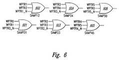
- FIG. 6illustrates another portion of the compare circuit 502 shown in FIG. 5 .
- Six three-input OR logic gates 601 - 606provide a respective one of the input signals SAMP 01 -SAMP 50 that are coupled to the inputs of the multiplexers 520 , 530 .
- the inputs of each of the OR gates 601 - 606are coupled to a different combination of the enable signals WPTR 0 -WPTR 5 , WPTR 0 _N-WPTR 5 _N provided by the write counter circuit 400 ( FIG. 4 ).
- the OR gates 601 - 606are conventional.
- the read pointer circuit 500 and the compare circuit 502can be substituted for the read pointer 316 and the compare circuit 320 of the read data synchronization circuit 300 .
- the write pointer circuit 400 , the read pointer circuit 500 , and the compare circuit 502can be used together to determine a write and read pointer offset for a read data synchronization circuit having a buffer with 12 data locations and a multiplexer that selects groups of 4 data locations of the buffer for coupling to a latch circuit.
- the write pointer circuit 400can be used to generate enable signals WPTR 0 -WPTR 5 , WPTR 0 _N-WPTR 5 _N for sequentially enabling one of twelve data locations of a buffer to which memory read data from a memory device is written.
- the write pointer circuit 400operates according to the RSTB signal, which essentially clocks at the same frequency as a memory clock signal.
- the enable signals WPTR 0 -WPTR 5 , WPTR 0 _N-WPTR 5 _Nare further coupled in various combinations to the input terminals of the OR gates 601 - 606 .
- the OR gates 601 - 606are used to generate signals that are indicative of the location of the write pointer.
- the OR gates 601 - 606generate signals indicative of the location of the “one-hot” bit for the D flip-flops 410 - 415 and 420 - 425 . Based on the location of the one-hot bits, an indication of which data location the write pointer is pointing is provided.
- the one-hot bit for the first set of D flip-flops 410 - 415is located at the D flip-flop 411 following a rising edge of the RSTB signal, the output of the OR gates 601 and 602 will be HIGH, while the output of the remaining OR gates 603 - 606 will remain LOW.
- the one-hot bit for the D flip-flops 420 - 425is located at the D flip-flop 421 , causing in the outputs of the OR gates 601 and 602 to remain HIGH and the outputs of the remaining D flip-flops 603 - 606 remain LOW.
- the one-hot bit of the D flip-flops 210 - 215moves to the D flip-flop 412 .
- the output of the OR gate 601switches LOW
- the output of the OR gate 602remains HIGH
- the output of the OR gate 603switches HIGH.
- the OR gates 604 - 606remain LOW.
- the one-hot bit for the D flip-flops 420 - 425moves to the D flip-flop 422 .
- the outputs of the OR gates 602 and 603remain HIGH, and the outputs of the remaining OR gates 601 and 604 - 606 remain LOW.
- the one-hot bit of the D flip-flops 410 - 415moves to the D flip-flop 413 , causing the output of the OR gate 602 to switch LOW and the output of the OR gate 604 to switch HIGH.
- the output of the OR gate 603remains HIGH and the outputs of the remaining OR gates 601 , 602 , 605 , 606 remain LOW.
- the location of the one-hot bits of the D flip-flops 410 - 415 , 420 - 425is represented by which two of the six OR gates 601 - 606 has HIGH output signals.
- a first of the two OR gates having a HIGH outputidentifies the “trailing” D flip-flop at which the one-hot bit is currently located or was just previously located, and a second of the two OR gates identifies the “leading” D flip-flop at which the one-hot bit is currently located or will soon be located.
- the one-hot arrangement of the D flip-flops 410 - 415 and 420 - 425facilitates determination of the write and read pointer offset by avoiding potential sampling errors present with an encoded write pointer scheme.
- An encoded schemedigitally encodes a value corresponding to the data location to which memory read data is written. For example, when using a three-bit encoded write pointer, pointing to the fourth data location of the 12-data location buffer is represented by 011. In response to the next clock transition of the RSTB signal, the write pointer will increment to 100.
- the read pointer circuit 500generates selection signal SEL for a multiplexer (not shown) that selects groups of four data locations of the 12-data location buffer in accordance with the CLK signal.
- the SEL signalis further used to sequentially select which of the six input signals from the OR gates 601 - 606 are coupled as a respective output signal of the multiplexers 520 , 530 .
- the respective outputs of the multiplexers 520 , 530are latched in response to the rising edge of the CLK signal by the D flip-flops 522 , 532 , and on the next rising edge of the CLK signal by the D flip-flops 524 , 534 to provide an OFFSET signal.
- the OFFSET signal provided by the D flip-flops 524 , 534is indicative of the write and read pointer offset.
- the memory controller 280receives the OFFSET signal from the compare circuit and uses the write and read pointer offset to determine whether timing parameters should be adjusted. For example, based on the write and read pointer offset, the memory controller 280 can determine whether the timing between issuance of a read command and when the data locations of the buffer are selected for providing the read data should be adjusted to relax or tighten the timing margin. Additionally, based on the write and read pointer offset, analysis of the timing between the issuance of a first memory command and a second memory command can be refined and modified to reduce command turn-around times if desirable.
Landscapes
- Engineering & Computer Science (AREA)
- Theoretical Computer Science (AREA)
- Physics & Mathematics (AREA)
- General Engineering & Computer Science (AREA)
- General Physics & Mathematics (AREA)
- Dram (AREA)
Abstract
Description
Claims (17)
Priority Applications (1)
| Application Number | Priority Date | Filing Date | Title |
|---|---|---|---|
| US12/553,856US8239607B2 (en) | 2004-06-04 | 2009-09-03 | System and method for an asynchronous data buffer having buffer write and read pointers |
Applications Claiming Priority (3)
| Application Number | Priority Date | Filing Date | Title |
|---|---|---|---|
| US10/861,145US7519788B2 (en) | 2004-06-04 | 2004-06-04 | System and method for an asynchronous data buffer having buffer write and read pointers |
| US11/418,897US7594088B2 (en) | 2004-06-04 | 2006-05-04 | System and method for an asynchronous data buffer having buffer write and read pointers |
| US12/553,856US8239607B2 (en) | 2004-06-04 | 2009-09-03 | System and method for an asynchronous data buffer having buffer write and read pointers |
Related Parent Applications (1)
| Application Number | Title | Priority Date | Filing Date |
|---|---|---|---|
| US11/418,897ContinuationUS7594088B2 (en) | 2004-06-04 | 2006-05-04 | System and method for an asynchronous data buffer having buffer write and read pointers |
Publications (2)
| Publication Number | Publication Date |
|---|---|
| US20090319745A1 US20090319745A1 (en) | 2009-12-24 |
| US8239607B2true US8239607B2 (en) | 2012-08-07 |
Family
ID=35505626
Family Applications (3)
| Application Number | Title | Priority Date | Filing Date |
|---|---|---|---|
| US10/861,145Active2027-01-25US7519788B2 (en) | 2004-06-04 | 2004-06-04 | System and method for an asynchronous data buffer having buffer write and read pointers |
| US11/418,897Active2026-03-28US7594088B2 (en) | 2004-06-04 | 2006-05-04 | System and method for an asynchronous data buffer having buffer write and read pointers |
| US12/553,856Expired - LifetimeUS8239607B2 (en) | 2004-06-04 | 2009-09-03 | System and method for an asynchronous data buffer having buffer write and read pointers |
Family Applications Before (2)
| Application Number | Title | Priority Date | Filing Date |
|---|---|---|---|
| US10/861,145Active2027-01-25US7519788B2 (en) | 2004-06-04 | 2004-06-04 | System and method for an asynchronous data buffer having buffer write and read pointers |
| US11/418,897Active2026-03-28US7594088B2 (en) | 2004-06-04 | 2006-05-04 | System and method for an asynchronous data buffer having buffer write and read pointers |
Country Status (1)
| Country | Link |
|---|---|
| US (3) | US7519788B2 (en) |
Cited By (7)
| Publication number | Priority date | Publication date | Assignee | Title |
|---|---|---|---|---|
| US20130182515A1 (en)* | 2012-01-17 | 2013-07-18 | Qualcomm Incorporated | Dual-voltage domain memory buffers, and related systems and methods |
| US8526249B1 (en)* | 2010-08-04 | 2013-09-03 | Marvell International Ltd. | Methods and systems for detecting and correcting timing signal drift in memory systems |
| US9589661B2 (en) | 2014-03-20 | 2017-03-07 | Samsung Electronics Co., Ltd. | Method of programming memory device and method of reading data of memory device including the same |
| US11113213B2 (en) | 2019-12-30 | 2021-09-07 | Micron Technology, Inc. | Determining write commands for deletion in a host interface |
| US11294592B2 (en) | 2018-01-09 | 2022-04-05 | Alibaba Group Holding Limited | Method and device for data processing, and computer device |
| US20230216653A1 (en)* | 2020-06-15 | 2023-07-06 | Ntt Electronics Corporation | Data transfer circuit and communication apparatus |
| US11907572B2 (en) | 2019-12-30 | 2024-02-20 | Micron Technology, Inc. | Interface read after write |
Families Citing this family (44)
| Publication number | Priority date | Publication date | Assignee | Title |
|---|---|---|---|---|
| US6791555B1 (en) | 2000-06-23 | 2004-09-14 | Micron Technology, Inc. | Apparatus and method for distributed memory control in a graphics processing system |
| US7133972B2 (en) | 2002-06-07 | 2006-11-07 | Micron Technology, Inc. | Memory hub with internal cache and/or memory access prediction |
| US7117316B2 (en) | 2002-08-05 | 2006-10-03 | Micron Technology, Inc. | Memory hub and access method having internal row caching |
| US6820181B2 (en) | 2002-08-29 | 2004-11-16 | Micron Technology, Inc. | Method and system for controlling memory accesses to memory modules having a memory hub architecture |
| US7120727B2 (en) | 2003-06-19 | 2006-10-10 | Micron Technology, Inc. | Reconfigurable memory module and method |
| US7260685B2 (en) | 2003-06-20 | 2007-08-21 | Micron Technology, Inc. | Memory hub and access method having internal prefetch buffers |
| US7107415B2 (en) | 2003-06-20 | 2006-09-12 | Micron Technology, Inc. | Posted write buffers and methods of posting write requests in memory modules |
| US7133991B2 (en)* | 2003-08-20 | 2006-11-07 | Micron Technology, Inc. | Method and system for capturing and bypassing memory transactions in a hub-based memory system |
| US7120743B2 (en) | 2003-10-20 | 2006-10-10 | Micron Technology, Inc. | Arbitration system and method for memory responses in a hub-based memory system |
| US7330992B2 (en) | 2003-12-29 | 2008-02-12 | Micron Technology, Inc. | System and method for read synchronization of memory modules |
| US7188219B2 (en) | 2004-01-30 | 2007-03-06 | Micron Technology, Inc. | Buffer control system and method for a memory system having outstanding read and write request buffers |
| US7213082B2 (en) | 2004-03-29 | 2007-05-01 | Micron Technology, Inc. | Memory hub and method for providing memory sequencing hints |
| US7162567B2 (en) | 2004-05-14 | 2007-01-09 | Micron Technology, Inc. | Memory hub and method for memory sequencing |
| US7519788B2 (en) | 2004-06-04 | 2009-04-14 | Micron Technology, Inc. | System and method for an asynchronous data buffer having buffer write and read pointers |
| US7401258B1 (en)* | 2004-09-30 | 2008-07-15 | Xilinx, Inc. | Circuit for and method of accessing instruction data written to a memory |
| US7966439B1 (en)* | 2004-11-24 | 2011-06-21 | Nvidia Corporation | Apparatus, system, and method for a fast data return memory controller |
| DE102005053294B4 (en)* | 2005-11-08 | 2008-03-27 | Qimonda Ag | Circuit arrangement for the time delay of read data, semiconductor memory circuit and method |
| US8059642B2 (en)* | 2006-02-09 | 2011-11-15 | Flextronics International Usa, Inc. | Single stage pointer and overhead processing |
| US7415569B2 (en)* | 2006-03-22 | 2008-08-19 | Infineon Technologies Ag | Memory including a write training block |
| US8185711B2 (en)* | 2006-05-16 | 2012-05-22 | Samsung Electronics Co., Ltd. | Memory module, a memory system including a memory controller and a memory module and methods thereof |
| JP2008152315A (en)* | 2006-12-14 | 2008-07-03 | Sanyo Electric Co Ltd | Signal processing circuit |
| WO2008079910A2 (en) | 2006-12-20 | 2008-07-03 | Rambus Inc. | Strobe acquisition and tracking |
| WO2008142610A1 (en)* | 2007-05-16 | 2008-11-27 | Nxp B.V. | Fifo buffer |
| US7958285B1 (en)* | 2007-07-12 | 2011-06-07 | Oracle America, Inc. | System and method to facilitate deterministic testing of data transfers between independent clock domains on a chip |
| US8289086B2 (en) | 2008-04-02 | 2012-10-16 | Qualcomm Atheros, Inc. | Fractional and integer PLL architectures |
| EP2466478B1 (en) | 2010-12-20 | 2013-11-27 | STMicroelectronics (Grenoble 2) SAS | Communication system, and corresponding integrated circuit and method |
| US9026761B2 (en)* | 2010-12-20 | 2015-05-05 | Stmicroelectronics (Grenoble 2) Sas | Interface system, and corresponding integrated circuit and method |
| US8995207B2 (en)* | 2011-08-12 | 2015-03-31 | Qualcomm Incorporated | Data storage for voltage domain crossings |
| TWI474147B (en)* | 2012-03-01 | 2015-02-21 | Realtek Semiconductor Corp | Modulating determination apparatus , modulating determination method, and power supply circuit thereof |
| US9712453B1 (en) | 2012-03-26 | 2017-07-18 | Amazon Technologies, Inc. | Adaptive throttling for shared resources |
| US8909878B2 (en)* | 2012-06-12 | 2014-12-09 | International Business Machines Corporation | Implementing timing alignment and synchronized memory activities of multiple memory devices accessed in parallel |
| CN102779016B (en)* | 2012-06-18 | 2015-06-24 | 上海卫星工程研究所 | Design method based on synchronous dynamic random access memory (SDRAM) satellite-bone storage subfile reading and writing |
| EP3058571A1 (en)* | 2013-10-15 | 2016-08-24 | Rambus Inc. | Load reduced memory module |
| US11132328B2 (en)* | 2013-12-20 | 2021-09-28 | Rambus, Inc. | High level instructions with lower-level assembly code style primitives within a memory appliance for accessing memory |
| DE102015209486A1 (en)* | 2015-05-22 | 2016-11-24 | Robert Bosch Gmbh | FIFO memory with operable memory area |
| US10719237B2 (en) | 2016-01-11 | 2020-07-21 | Micron Technology, Inc. | Apparatuses and methods for concurrently accessing multiple partitions of a non-volatile memory |
| US10534540B2 (en)* | 2016-06-06 | 2020-01-14 | Micron Technology, Inc. | Memory protocol |
| US10168731B2 (en)* | 2016-07-13 | 2019-01-01 | Advanced Micro Devices, Inc. | Managing frequency changes of clock signals across different clock domains |
| CN109800186B (en)* | 2017-11-17 | 2022-06-24 | 英业达科技有限公司 | Control system and control method thereof |
| US10592442B2 (en)* | 2017-12-11 | 2020-03-17 | Advanced Micro Devices, Inc. | Asynchronous buffer with pointer offsets |
| CN109299146B (en)* | 2018-09-18 | 2020-09-25 | 交控科技股份有限公司 | Data synchronization system and method |
| KR102802463B1 (en) | 2019-08-05 | 2025-05-02 | 에스케이하이닉스 주식회사 | Stack Type Semiconductor Apparatus |
| US20230186142A1 (en)* | 2021-12-13 | 2023-06-15 | Intel Corporation | Technologies for high-speed interfaces for cryogenic quantum control |
| JP7544823B2 (en)* | 2022-02-24 | 2024-09-03 | チャンシン メモリー テクノロジーズ インコーポレイテッド | Data transmission circuit, data transmission method and memory |
Citations (300)
| Publication number | Priority date | Publication date | Assignee | Title |
|---|---|---|---|---|
| US4045781A (en) | 1976-02-13 | 1977-08-30 | Digital Equipment Corporation | Memory module with selectable byte addressing for digital data processing system |
| US4240143A (en) | 1978-12-22 | 1980-12-16 | Burroughs Corporation | Hierarchical multi-processor network for memory sharing |
| US4245306A (en) | 1978-12-21 | 1981-01-13 | Burroughs Corporation | Selection of addressed processor in a multi-processor network |
| US4253146A (en) | 1978-12-21 | 1981-02-24 | Burroughs Corporation | Module for coupling computer-processors |
| US4253144A (en) | 1978-12-21 | 1981-02-24 | Burroughs Corporation | Multi-processor communication network |
| US4608702A (en) | 1984-12-21 | 1986-08-26 | Advanced Micro Devices, Inc. | Method for digital clock recovery from Manchester-encoded signals |
| US4707823A (en) | 1986-07-21 | 1987-11-17 | Chrysler Motors Corporation | Fiber optic multiplexed data acquisition system |
| US4724520A (en) | 1985-07-01 | 1988-02-09 | United Technologies Corporation | Modular multiport data hub |
| US4891808A (en) | 1987-12-24 | 1990-01-02 | Coherent Communication Systems Corp. | Self-synchronizing multiplexer |
| US4930128A (en) | 1987-06-26 | 1990-05-29 | Hitachi, Ltd. | Method for restart of online computer system and apparatus for carrying out the same |
| US4953930A (en) | 1989-03-15 | 1990-09-04 | Ramtech, Inc. | CPU socket supporting socket-to-socket optical communications |
| EP0395559A2 (en) | 1989-04-25 | 1990-10-31 | International Business Machines Corporation | Distributed cache dram chip |
| GB2244157A (en) | 1990-05-15 | 1991-11-20 | Sun Microsystems Inc | Apparatus for row caching in random access memory |
| US5133059A (en) | 1987-07-30 | 1992-07-21 | Alliant Computer Systems Corporation | Computer with multiple processors having varying priorities for access to a multi-element memory |
| US5241506A (en) | 1989-11-15 | 1993-08-31 | Kabushiki Kaisha Toshiba | Semiconductor memory circuit apparatus |
| US5243703A (en) | 1990-04-18 | 1993-09-07 | Rambus, Inc. | Apparatus for synchronously generating clock signals in a data processing system |
| US5251303A (en) | 1989-01-13 | 1993-10-05 | International Business Machines Corporation | System for DMA block data transfer based on linked control blocks |
| US5269022A (en) | 1990-03-28 | 1993-12-07 | Kabushiki Kaisha Toshiba | Method and apparatus for booting a computer system by restoring the main memory from a backup memory |
| US5317752A (en) | 1989-12-22 | 1994-05-31 | Tandem Computers Incorporated | Fault-tolerant computer system with auto-restart after power-fall |
| US5319755A (en) | 1990-04-18 | 1994-06-07 | Rambus, Inc. | Integrated circuit I/O using high performance bus interface |
| US5327553A (en) | 1989-12-22 | 1994-07-05 | Tandem Computers Incorporated | Fault-tolerant computer system with /CONFIG filesystem |
| US5355391A (en) | 1992-03-06 | 1994-10-11 | Rambus, Inc. | High speed bus system |
| US5432907A (en) | 1992-05-12 | 1995-07-11 | Network Resources Corporation | Network hub with integrated bridge |
| US5432823A (en) | 1992-03-06 | 1995-07-11 | Rambus, Inc. | Method and circuitry for minimizing clock-data skew in a bus system |
| US5442770A (en) | 1989-01-24 | 1995-08-15 | Nec Electronics, Inc. | Triple port cache memory |
| US5461627A (en) | 1991-12-24 | 1995-10-24 | Rypinski; Chandos A. | Access protocol for a common channel wireless network |
| US5465343A (en) | 1993-04-30 | 1995-11-07 | Quantum Corporation | Shared memory array for data block and control program storage in disk drive |
| US5465229A (en) | 1992-05-19 | 1995-11-07 | Sun Microsystems, Inc. | Single in-line memory module |
| US5479370A (en) | 1992-02-20 | 1995-12-26 | Kabushiki Kaisha Toshiba | Semiconductor memory with bypass circuit |
| US5497476A (en) | 1992-09-21 | 1996-03-05 | International Business Machines Corporation | Scatter-gather in data processing system |
| US5502621A (en) | 1994-03-31 | 1996-03-26 | Hewlett-Packard Company | Mirrored pin assignment for two sided multi-chip layout |
| US5544319A (en) | 1992-03-25 | 1996-08-06 | Encore Computer U.S., Inc. | Fiber optic memory coupling system with converter transmitting and receiving bus data in parallel fashion and diagnostic data in serial fashion |
| US5566325A (en) | 1994-06-30 | 1996-10-15 | Digital Equipment Corporation | Method and apparatus for adaptive memory access |
| US5577220A (en) | 1993-07-23 | 1996-11-19 | International Business Machines Corporation | Method for saving and restoring the state of a CPU executing code in protected mode including estimating the value of the page table base register |
| US5581767A (en) | 1993-06-16 | 1996-12-03 | Nippon Sheet Glass Co., Ltd. | Bus structure for multiprocessor system having separated processor section and control/memory section |
| US5613075A (en) | 1993-11-12 | 1997-03-18 | Intel Corporation | Method and apparatus for providing deterministic read access to main memory in a computer system |
| US5619670A (en) | 1993-07-26 | 1997-04-08 | Nec Corporation | Address decoder with small circuit scale and address area expansion capability |
| US5638534A (en) | 1995-03-31 | 1997-06-10 | Samsung Electronics Co., Ltd. | Memory controller which executes read and write commands out of order |
| US5659713A (en) | 1992-04-24 | 1997-08-19 | Digital Equipment Corporation | Memory stream buffer with variable-size prefetch depending on memory interleaving configuration |
| US5659798A (en) | 1996-02-02 | 1997-08-19 | Blumrich; Matthias Augustin | Method and system for initiating and loading DMA controller registers by using user-level programs |
| US5706224A (en) | 1996-10-10 | 1998-01-06 | Quality Semiconductor, Inc. | Content addressable memory and random access memory partition circuit |
| US5715456A (en) | 1995-02-13 | 1998-02-03 | International Business Machines Corporation | Method and apparatus for booting a computer system without pre-installing an operating system |
| US5729709A (en) | 1993-11-12 | 1998-03-17 | Intel Corporation | Memory controller with burst addressing circuit |
| US5748616A (en) | 1994-09-13 | 1998-05-05 | Square D Company | Data link module for time division multiplexing control systems |
| EP0843261A2 (en) | 1996-11-18 | 1998-05-20 | Nec Corporation | Virtual channel memory system |
| EP0849685A2 (en) | 1996-12-19 | 1998-06-24 | Texas Instruments Incorporated | Communication bus system between processors and memory modules |
| US5796413A (en) | 1995-12-06 | 1998-08-18 | Compaq Computer Corporation | Graphics controller utilizing video memory to provide macro command capability and enhanched command buffering |
| US5818844A (en) | 1996-06-06 | 1998-10-06 | Advanced Micro Devices, Inc. | Address generation and data path arbitration to and from SRAM to accommodate multiple transmitted packets |
| US5819304A (en) | 1996-01-29 | 1998-10-06 | Iowa State University Research Foundation, Inc. | Random access memory assembly |
| US5822255A (en) | 1996-08-13 | 1998-10-13 | Fujitsu Limited | Semiconductor integrated circuit for supplying a control signal to a plurality of object circuits |
| US5832250A (en) | 1996-01-26 | 1998-11-03 | Unisys Corporation | Multi set cache structure having parity RAMs holding parity bits for tag data and for status data utilizing prediction circuitry that predicts and generates the needed parity bits |
| US5838931A (en) | 1994-12-08 | 1998-11-17 | Intel Corporation | Method and apparatus for enabling a processor to access an external component through a private bus or a shared bus |
| US5875352A (en) | 1995-11-03 | 1999-02-23 | Sun Microsystems, Inc. | Method and apparatus for multiple channel direct memory access control |
| US5875454A (en) | 1996-07-24 | 1999-02-23 | International Business Machiness Corporation | Compressed data cache storage system |
| US5887159A (en) | 1996-12-11 | 1999-03-23 | Digital Equipment Corporation | Dynamically determining instruction hint fields |
| US5889714A (en) | 1997-11-03 | 1999-03-30 | Digital Equipment Corporation | Adaptive precharge management for synchronous DRAM |
| US5953743A (en) | 1997-03-12 | 1999-09-14 | Micron Electronics, Inc. | Method for accelerating memory bandwidth |
| US5966724A (en) | 1996-01-11 | 1999-10-12 | Micron Technology, Inc. | Synchronous memory device with dual page and burst mode operations |
| US5973935A (en) | 1997-04-07 | 1999-10-26 | Micron Technology, Inc. | Interdigitated leads-over-chip lead frame for supporting an integrated circuit die |
| US5978567A (en) | 1994-07-27 | 1999-11-02 | Instant Video Technologies Inc. | System for distribution of interactive multimedia and linear programs by enabling program webs which include control scripts to define presentation by client transceiver |
| US5987196A (en) | 1997-11-06 | 1999-11-16 | Micron Technology, Inc. | Semiconductor structure having an optical signal path in a substrate and method for forming the same |
| US6006340A (en)* | 1998-03-27 | 1999-12-21 | Phoenix Technologies Ltd. | Communication interface between two finite state machines operating at different clock domains |
| US6023726A (en) | 1998-01-20 | 2000-02-08 | Netscape Communications Corporation | User configurable prefetch control system for enabling client to prefetch documents from a network server |
| US6029250A (en) | 1998-09-09 | 2000-02-22 | Micron Technology, Inc. | Method and apparatus for adaptively adjusting the timing offset between a clock signal and digital signals transmitted coincident with that clock signal, and memory device and system using same |
| US6031241A (en) | 1997-03-11 | 2000-02-29 | University Of Central Florida | Capillary discharge extreme ultraviolet lamp source for EUV microlithography and other related applications |
| US6033951A (en) | 1996-08-16 | 2000-03-07 | United Microelectronics Corp. | Process for fabricating a storage capacitor for semiconductor memory devices |
| TW387072B (en) | 1997-04-04 | 2000-04-11 | Ibm | Low latency first data access in a data buffered smp memory controller |
| US6061263A (en) | 1998-12-29 | 2000-05-09 | Intel Corporation | Small outline rambus in-line memory module |
| US6061296A (en) | 1998-08-17 | 2000-05-09 | Vanguard International Semiconductor Corporation | Multiple data clock activation with programmable delay for use in multiple CAS latency memory devices |
| US6067262A (en) | 1998-12-11 | 2000-05-23 | Lsi Logic Corporation | Redundancy analysis for embedded memories with built-in self test and built-in self repair |
| US6073190A (en) | 1997-07-18 | 2000-06-06 | Micron Electronics, Inc. | System for dynamic buffer allocation comprising control logic for controlling a first address buffer and a first data buffer as a matched pair |
| US6076139A (en) | 1996-12-31 | 2000-06-13 | Compaq Computer Corporation | Multimedia computer architecture with multi-channel concurrent memory access |
| US6079008A (en) | 1998-04-03 | 2000-06-20 | Patton Electronics Co. | Multiple thread multiple data predictive coded parallel processing system and method |
| US6092158A (en) | 1997-06-13 | 2000-07-18 | Intel Corporation | Method and apparatus for arbitrating between command streams |
| US6098158A (en) | 1997-12-18 | 2000-08-01 | International Business Machines Corporation | Software-enabled fast boot |
| US6105075A (en) | 1997-08-05 | 2000-08-15 | Adaptec, Inc. | Scatter gather memory system for a hardware accelerated command interpreter engine |
| US6111757A (en) | 1998-01-16 | 2000-08-29 | International Business Machines Corp. | SIMM/DIMM memory module |
| US6125431A (en) | 1996-08-02 | 2000-09-26 | Oki Electric Industry Co., Ltd. | Single-chip microcomputer using adjustable timing to fetch data from an external memory |
| JP2000268006A (en) | 1999-03-15 | 2000-09-29 | Fuji Xerox Co Ltd | Multiprocessor system |
| US6128703A (en) | 1997-09-05 | 2000-10-03 | Integrated Device Technology, Inc. | Method and apparatus for memory prefetch operation of volatile non-coherent data |
| US6128706A (en) | 1998-02-03 | 2000-10-03 | Institute For The Development Of Emerging Architectures, L.L.C. | Apparatus and method for a load bias--load with intent to semaphore |
| US6131149A (en) | 1997-06-04 | 2000-10-10 | Oak Technology, Inc. | Apparatus and method for reading data from synchronous memory with skewed clock pulses |
| US6134624A (en) | 1998-06-08 | 2000-10-17 | Storage Technology Corporation | High bandwidth cache system |
| US6145033A (en) | 1998-07-17 | 2000-11-07 | Seiko Epson Corporation | Management of display FIFO requests for DRAM access wherein low priority requests are initiated when FIFO level is below/equal to high threshold value |
| US6144587A (en) | 1998-06-23 | 2000-11-07 | Nec Corporation | Semiconductor memory device |
| KR20000067533A (en) | 1999-04-29 | 2000-11-25 | 한탁돈 | Memory access system and method thereof |
| US6157962A (en) | 1996-02-05 | 2000-12-05 | International Business Machines Corporation | Multipath I/O storage systems with multiipath I/O request mechanisms |
| US6157743A (en) | 1998-07-31 | 2000-12-05 | Hewlett Packard Company | Method for retrieving compressed texture data from a memory system |
| US6167465A (en) | 1998-05-20 | 2000-12-26 | Aureal Semiconductor, Inc. | System for managing multiple DMA connections between a peripheral device and a memory and performing real-time operations on data carried by a selected DMA connection |
| US6175571B1 (en) | 1994-07-22 | 2001-01-16 | Network Peripherals, Inc. | Distributed memory switching hub |
| US6185676B1 (en) | 1997-09-30 | 2001-02-06 | Intel Corporation | Method and apparatus for performing early branch prediction in a microprocessor |
| US6185352B1 (en) | 2000-02-24 | 2001-02-06 | Siecor Operations, Llc | Optical fiber ribbon fan-out cables |
| US6186400B1 (en) | 1998-03-20 | 2001-02-13 | Symbol Technologies, Inc. | Bar code reader with an integrated scanning component module mountable on printed circuit board |
| US6191663B1 (en) | 1998-12-22 | 2001-02-20 | Intel Corporation | Echo reduction on bit-serial, multi-drop bus |
| US6201724B1 (en) | 1998-11-12 | 2001-03-13 | Nec Corporation | Semiconductor memory having improved register array access speed |
| US6208180B1 (en) | 1995-12-29 | 2001-03-27 | Intel Corporation | Core clock correction in a 2/N mode clocking scheme |
| US6212590B1 (en) | 1997-12-22 | 2001-04-03 | Compaq Computer Corporation | Computer system having integrated bus bridge design with delayed transaction arbitration mechanism employed within laptop computer docked to expansion base |
| US6216219B1 (en) | 1996-12-31 | 2001-04-10 | Texas Instruments Incorporated | Microprocessor circuits, systems, and methods implementing a load target buffer with entries relating to prefetch desirability |
| US6216178B1 (en) | 1998-11-16 | 2001-04-10 | Infineon Technologies Ag | Methods and apparatus for detecting the collision of data on a data bus in case of out-of-order memory accesses of different times of memory access execution |
| US6219725B1 (en) | 1998-08-28 | 2001-04-17 | Hewlett-Packard Company | Method and apparatus for performing direct memory access transfers involving non-sequentially-addressable memory locations |
| US6223301B1 (en) | 1997-09-30 | 2001-04-24 | Compaq Computer Corporation | Fault tolerant memory |
| US6223259B1 (en) | 1998-10-30 | 2001-04-24 | Telefonaktiebolaget Lm Ericsson (Publ) | Reducing read cycle of memory read request for data to be partially modified by a pending write request |
| US6233376B1 (en) | 1999-05-18 | 2001-05-15 | The United States Of America As Represented By The Secretary Of The Navy | Embedded fiber optic circuit boards and integrated circuits |
| US6243831B1 (en) | 1998-10-31 | 2001-06-05 | Compaq Computer Corporation | Computer system with power loss protection mechanism |
| US6243769B1 (en) | 1997-07-18 | 2001-06-05 | Micron Technology, Inc. | Dynamic buffer allocation for a computer system |
| US6246618B1 (en) | 2000-06-30 | 2001-06-12 | Mitsubishi Denki Kabushiki Kaisha | Semiconductor integrated circuit capable of testing and substituting defective memories and method thereof |
| US6247107B1 (en) | 1998-04-06 | 2001-06-12 | Advanced Micro Devices, Inc. | Chipset configured to perform data-directed prefetching |
| US6249802B1 (en) | 1997-09-19 | 2001-06-19 | Silicon Graphics, Inc. | Method, system, and computer program product for allocating physical memory in a distributed shared memory network |
| US6252821B1 (en) | 1999-12-29 | 2001-06-26 | Intel Corporation | Method and apparatus for memory address decode in memory subsystems supporting a large number of memory devices |
| US6256692B1 (en) | 1997-10-13 | 2001-07-03 | Fujitsu Limited | CardBus interface circuit, and a CardBus PC having the same |
| US6266730B1 (en) | 1997-09-26 | 2001-07-24 | Rambus Inc. | High-frequency bus system |
| US6272609B1 (en) | 1998-07-31 | 2001-08-07 | Micron Electronics, Inc. | Pipelined memory controller |
| US6285349B1 (en) | 1999-02-26 | 2001-09-04 | Intel Corporation | Correcting non-uniformity in displays |
| US6286083B1 (en) | 1998-07-08 | 2001-09-04 | Compaq Computer Corporation | Computer system with adaptive memory arbitration scheme |
| US6294937B1 (en) | 1999-05-25 | 2001-09-25 | Lsi Logic Corporation | Method and apparatus for self correcting parallel I/O circuitry |
| JP2001265539A (en) | 2000-03-16 | 2001-09-28 | Fuji Xerox Co Ltd | Array type storage device and information processing system |
| US6301637B1 (en) | 1998-06-08 | 2001-10-09 | Storage Technology Corporation | High performance data paths |
| US20010039612A1 (en) | 1999-12-02 | 2001-11-08 | Lee Sang-Jin | Apparatus and method for fast booting |
| US6321233B1 (en) | 1998-12-15 | 2001-11-20 | Micron Technology, Inc. | Apparatus for controlling pipelined memory access requests |
| US6330639B1 (en) | 1999-06-29 | 2001-12-11 | Intel Corporation | Method and apparatus for dynamically changing the sizes of pools that control the power consumption levels of memory devices |
| US6330205B2 (en) | 1999-12-22 | 2001-12-11 | Nec Corporation | Virtual channel synchronous dynamic random access memory |
| US20020002656A1 (en) | 1997-01-29 | 2002-01-03 | Ichiki Honma | Information processing system |
| US6347055B1 (en) | 1999-06-24 | 2002-02-12 | Nec Corporation | Line buffer type semiconductor memory device capable of direct prefetch and restore operations |
| US6349363B2 (en) | 1998-12-08 | 2002-02-19 | Intel Corporation | Multi-section cache with different attributes for each section |
| US6356573B1 (en) | 1998-01-31 | 2002-03-12 | Mitel Semiconductor Ab | Vertical cavity surface emitting laser |
| US6367074B1 (en) | 1998-12-28 | 2002-04-02 | Intel Corporation | Operation of a system |
| WO2002027499A2 (en) | 2000-09-29 | 2002-04-04 | Intel Corporation | Shared translation address caching |
| US6370068B2 (en) | 2000-01-05 | 2002-04-09 | Samsung Electronics Co., Ltd. | Semiconductor memory devices and methods for sampling data therefrom based on a relative position of a memory cell array section containing the data |
| US6370611B1 (en) | 2000-04-04 | 2002-04-09 | Compaq Computer Corporation | Raid XOR operations to synchronous DRAM using a read buffer and pipelining of synchronous DRAM burst read data |
| US6373777B1 (en) | 1998-07-14 | 2002-04-16 | Nec Corporation | Semiconductor memory |
| EP1199637A2 (en) | 2000-10-17 | 2002-04-24 | Hitachi, Ltd. | Disk controller comprising cache memory and method of controlling the cache |
| US6381190B1 (en) | 1999-05-13 | 2002-04-30 | Nec Corporation | Semiconductor memory device in which use of cache can be selected |
| US6389514B1 (en) | 1999-03-25 | 2002-05-14 | Hewlett-Packard Company | Method and computer system for speculatively closing pages in memory |
| US6392653B1 (en) | 1998-06-25 | 2002-05-21 | Inria Institut National De Recherche En Informatique Et En Automatique | Device for processing acquisition data, in particular image data |
| US6401149B1 (en) | 1999-05-05 | 2002-06-04 | Qlogic Corporation | Methods for context switching within a disk controller |
| US6401213B1 (en) | 1999-07-09 | 2002-06-04 | Micron Technology, Inc. | Timing circuit for high speed memory |
| US6405280B1 (en) | 1998-06-05 | 2002-06-11 | Micron Technology, Inc. | Packet-oriented synchronous DRAM interface supporting a plurality of orderings for data block transfers within a burst sequence |
| US20020078298A1 (en) | 1999-01-29 | 2002-06-20 | Joseph M. Jeddeloh | Method to access memory based on a programmable page limit |
| TW491970B (en) | 2000-06-29 | 2002-06-21 | Silicon Integrated Sys Corp | Page collector for improving performance of a memory |
| US6421744B1 (en) | 1999-10-25 | 2002-07-16 | Motorola, Inc. | Direct memory access controller and method therefor |
| US6430696B1 (en) | 1998-11-30 | 2002-08-06 | Micron Technology, Inc. | Method and apparatus for high speed data capture utilizing bit-to-bit timing correction, and memory device using same |
| US6434696B1 (en) | 1998-05-11 | 2002-08-13 | Lg Electronics Inc. | Method for quickly booting a computer system |
| US6434736B1 (en) | 1999-07-08 | 2002-08-13 | Intel Corporation | Location based timing scheme in memory design |
| US6434639B1 (en) | 1998-11-13 | 2002-08-13 | Intel Corporation | System for combining requests associated with one or more memory locations that are collectively associated with a single cache line to furnish a single memory operation |
| US6433785B1 (en) | 1999-04-09 | 2002-08-13 | Intel Corporation | Method and apparatus for improving processor to graphics device throughput |
| US20020112119A1 (en) | 1998-02-13 | 2002-08-15 | Intel Corporation | Dual-port buffer-to-memory interface |
| JP2002232890A (en) | 2001-02-01 | 2002-08-16 | Sony Corp | Block distortion reduction circuit, reproducing device, receiver, block distortion reduction method |
| US6438622B1 (en) | 1998-11-17 | 2002-08-20 | Intel Corporation | Multiprocessor system including a docking system |
| US6438668B1 (en) | 1999-09-30 | 2002-08-20 | Apple Computer, Inc. | Method and apparatus for reducing power consumption in a digital processing system |
| US20020116588A1 (en) | 2000-12-20 | 2002-08-22 | Beckert Richard Dennis | Software management systems and methods for automotive computing devices |
| US20020120709A1 (en) | 2001-02-13 | 2002-08-29 | Matsushita Electric Industrial Co., Ltd. | Shared-memory controller for use in a multimedia processor system |
| US6449308B1 (en) | 1999-05-25 | 2002-09-10 | Intel Corporation | High-speed digital distribution system |
| US6453393B1 (en) | 2000-09-18 | 2002-09-17 | Intel Corporation | Method and apparatus for interfacing to a computer memory |
| US6457116B1 (en) | 1997-10-31 | 2002-09-24 | Broadcom Corporation | Method and apparatus for controlling contexts of multiple context processing elements in a network of multiple context processing elements |
| US6460114B1 (en) | 1999-07-29 | 2002-10-01 | Micron Technology, Inc. | Storing a flushed cache line in a memory buffer of a controller |
| US6460108B1 (en) | 1999-03-31 | 2002-10-01 | Intel Corporation | Low cost data streaming mechanism |
| US20020144064A1 (en) | 2001-03-30 | 2002-10-03 | Fanning Blaise B. | Controlling cache memory in external chipset using processor |
| US6463059B1 (en) | 1998-12-04 | 2002-10-08 | Koninklijke Philips Electronics N.V. | Direct memory access execution engine with indirect addressing of circular queues in addition to direct memory addressing |
| US6462978B2 (en) | 1997-08-21 | 2002-10-08 | Hitachi, Ltd. | Method of designing semiconductor integrated circuit device and semiconductor integrated circuit device |
| US6467013B1 (en) | 1999-09-30 | 2002-10-15 | Intel Corporation | Memory transceiver to couple an additional memory channel to an existing memory channel |
| US6473828B1 (en) | 1998-07-03 | 2002-10-29 | Nec Corporation | Virtual channel synchronous dynamic random access memory |
| US6477614B1 (en) | 1998-09-30 | 2002-11-05 | Intel Corporation | Method for implementing multiple memory buses on a memory module |
| US6477592B1 (en) | 1999-08-06 | 2002-11-05 | Integrated Memory Logic, Inc. | System for I/O interfacing for semiconductor chip utilizing addition of reference element to each data element in first data stream and interpret to recover data elements of second data stream |
| US6479322B2 (en) | 1998-06-01 | 2002-11-12 | Hitachi, Ltd. | Semiconductor device with two stacked chips in one resin body and method of producing |
| US6487628B1 (en) | 1999-03-31 | 2002-11-26 | Compaq Computer Corporation | Peripheral component interface with multiple data channels and reduced latency over a system area network |
| US20020178319A1 (en) | 2001-05-24 | 2002-11-28 | Jorge Sanchez-Olea | Optical bus arrangement for computer system |
| US6490188B2 (en) | 1999-09-02 | 2002-12-03 | Micron Technology, Inc. | Semiconductor devices having mirrored terminal arrangements, devices including same, and methods of testing such semiconductor devices |
| US6493803B1 (en) | 1999-08-23 | 2002-12-10 | Advanced Micro Devices, Inc. | Direct memory access controller with channel width configurability support |
| US6496193B1 (en) | 1999-12-30 | 2002-12-17 | Intel Corporation | Method and apparatus for fast loading of texture data into a tiled memory |
| US6496909B1 (en) | 1999-04-06 | 2002-12-17 | Silicon Graphics, Inc. | Method for managing concurrent access to virtual memory data structures |
| US6501471B1 (en) | 1999-12-13 | 2002-12-31 | Intel Corporation | Volume rendering |
| US6502161B1 (en) | 2000-01-05 | 2002-12-31 | Rambus Inc. | Memory system including a point-to-point linked memory subsystem |
| US20030005223A1 (en) | 2001-06-27 | 2003-01-02 | Coulson Richard L. | System boot time reduction method |
| US6505287B2 (en) | 1999-12-20 | 2003-01-07 | Nec Corporation | Virtual channel memory access controlling circuit |
| US20030014578A1 (en) | 2001-07-11 | 2003-01-16 | Pax George E. | Routability for memeory devices |
| US6523093B1 (en) | 2000-09-29 | 2003-02-18 | Intel Corporation | Prefetch buffer allocation and filtering system |
| US6523092B1 (en) | 2000-09-29 | 2003-02-18 | Intel Corporation | Cache line replacement policy enhancement to avoid memory page thrashing |
| US6526483B1 (en) | 2000-09-20 | 2003-02-25 | Broadcom Corporation | Page open hint in transactions |
| US20030043158A1 (en) | 2001-05-18 | 2003-03-06 | Wasserman Michael A. | Method and apparatus for reducing inefficiencies in shared memory devices |
| US20030043426A1 (en) | 2001-08-30 | 2003-03-06 | Baker R. J. | Optical interconnect in high-speed memory systems |
| US6539490B1 (en) | 1999-08-30 | 2003-03-25 | Micron Technology, Inc. | Clock distribution without clock delay or skew |
| US6553476B1 (en) | 1997-02-10 | 2003-04-22 | Matsushita Electric Industrial Co., Ltd. | Storage management based on predicted I/O execution times |
| US6552564B1 (en) | 1999-08-30 | 2003-04-22 | Micron Technology, Inc. | Technique to reduce reflections and ringing on CMOS interconnections |
| US6564329B1 (en) | 1999-03-16 | 2003-05-13 | Linkup Systems Corporation | System and method for dynamic clock generation |
| US20030093630A1 (en) | 2001-11-15 | 2003-05-15 | Richard Elizabeth A. | Techniques for processing out-of -order requests in a processor-based system |
| US6590816B2 (en) | 2001-03-05 | 2003-07-08 | Infineon Technologies Ag | Integrated memory and method for testing and repairing the integrated memory |
| US6594713B1 (en) | 1999-09-10 | 2003-07-15 | Texas Instruments Incorporated | Hub interface unit and application unit interfaces for expanded direct memory access processor |
| US6594722B1 (en) | 2000-06-29 | 2003-07-15 | Intel Corporation | Mechanism for managing multiple out-of-order packet streams in a PCI host bridge |
| US6598154B1 (en) | 1998-12-29 | 2003-07-22 | Intel Corporation | Precoding branch instructions to reduce branch-penalty in pipelined processors |
| US20030149809A1 (en) | 2001-08-29 | 2003-08-07 | Jensen Poul R. | Method and apparatus for timing and event processing in wireless systems |
| US20030158995A1 (en) | 2002-02-15 | 2003-08-21 | Ming-Hsien Lee | Method for DRAM control with adjustable page size |
| US20030156639A1 (en) | 2002-02-19 | 2003-08-21 | Jui Liang | Frame rate control system and method |
| US6611884B2 (en)* | 1999-02-05 | 2003-08-26 | Broadcom Corp | Self-adjusting elasticity data buffer with preload value |
| US20030163649A1 (en) | 2002-02-25 | 2003-08-28 | Kapur Suvansh K. | Shared bypass bus structure |
| US6615325B2 (en) | 1996-01-11 | 2003-09-02 | Micron Technology, Inc. | Method for switching between modes of operation |
| US6622227B2 (en) | 2000-12-27 | 2003-09-16 | Intel Corporation | Method and apparatus for utilizing write buffers in memory control/interface |
| US6628294B1 (en) | 1999-12-31 | 2003-09-30 | Intel Corporation | Prefetching of virtual-to-physical address translation for display data |
| US6629220B1 (en) | 1999-08-20 | 2003-09-30 | Intel Corporation | Method and apparatus for dynamic arbitration between a first queue and a second queue based on a high priority transaction type |
| US6631440B2 (en) | 2000-11-30 | 2003-10-07 | Hewlett-Packard Development Company | Method and apparatus for scheduling memory calibrations based on transactions |
| US6633959B2 (en) | 2001-06-21 | 2003-10-14 | International Business Machines Corporation | Non-uniform memory access (NUMA) data processing system that provides notification of remote deallocation of shared data |
| US20030193927A1 (en) | 2002-04-10 | 2003-10-16 | Stanley Hronik | Random access memory architecture and serial interface with continuous packet handling capability |
| US6636110B1 (en) | 1998-05-01 | 2003-10-21 | Mitsubishi Denki Kabushiki Kaisha | Internal clock generating circuit for clock synchronous semiconductor memory device |
| US6647470B1 (en) | 2000-08-21 | 2003-11-11 | Micron Technology, Inc. | Memory device having posted write per command |
| US6646929B1 (en) | 2001-12-05 | 2003-11-11 | Lsi Logic Corporation | Methods and structure for read data synchronization with minimal latency |
| US20030215042A1 (en) | 2002-05-17 | 2003-11-20 | Claude R. Gauthier | Adjustment and calibration system for post-fabrication treatment of phase locked loop input receiver |
| US20030217223A1 (en) | 2002-05-14 | 2003-11-20 | Infineon Technologies North America Corp. | Combined command set |
| US6658509B1 (en) | 2000-10-03 | 2003-12-02 | Intel Corporation | Multi-tier point-to-point ring memory interface |
| US20030223295A1 (en) | 2002-01-17 | 2003-12-04 | Ozguz Volkan H. | Field programmable gate array with a variably wide word width memory |
| US6662304B2 (en) | 1998-12-11 | 2003-12-09 | Micron Technology, Inc. | Method and apparatus for bit-to-bit timing correction of a high speed memory bus |
| US20030229762A1 (en) | 2002-06-11 | 2003-12-11 | Subramaniam Maiyuran | Apparatus, method, and system for synchronizing information prefetch between processors and memory controllers |
| US20030227798A1 (en) | 2002-06-07 | 2003-12-11 | Pax George E | Reduced power registered memory module and method |
| US6665202B2 (en) | 2001-09-25 | 2003-12-16 | Integrated Device Technology, Inc. | Content addressable memory (CAM) devices that can identify highest priority matches in non-sectored CAM arrays and methods of operating same |
| US6667895B2 (en) | 2001-12-06 | 2003-12-23 | Samsung Electronics Co., Ltd. | Integrated circuit device and module with integrated circuits |
| US20030235072A1 (en) | 2002-06-22 | 2003-12-25 | Tae-Wan Kim | Magnetic random access memory (MRAM) for spontaneous hall effect and method of writing and reading data using the MRAM |
| US20040006671A1 (en) | 2002-07-05 | 2004-01-08 | Handgen Erin Antony | Method and system for optimizing pre-fetch memory transactions |
| US6681292B2 (en) | 2001-08-27 | 2004-01-20 | Intel Corporation | Distributed read and write caching implementation for optimized input/output applications |
| US20040015666A1 (en)* | 2002-07-19 | 2004-01-22 | Edmundo Rojas | Method and apparatus for asynchronous read control |
| US20040019728A1 (en) | 2002-07-23 | 2004-01-29 | Sharma Debendra Das | Multiple hardware partitions under one input/output hub |
| US20040024959A1 (en) | 2002-08-02 | 2004-02-05 | Taylor George R. | System and method for optically interconnecting memory devices |
| US20040034753A1 (en) | 2002-08-16 | 2004-02-19 | Jeddeloh Joseph M. | Memory hub bypass circuit and method |
| US6697926B2 (en) | 2001-06-06 | 2004-02-24 | Micron Technology, Inc. | Method and apparatus for determining actual write latency and accurately aligning the start of data capture with the arrival of data at a memory device |
| US20040039886A1 (en) | 2002-08-26 | 2004-02-26 | International Business Machines Corporation | Dynamic cache disable |
| US20040044833A1 (en) | 2002-08-29 | 2004-03-04 | Ryan Kevin J. | System and method for optimizing interconnections of memory devices in a multichip module |
| US6704817B1 (en) | 2000-08-31 | 2004-03-09 | Hewlett-Packard Development Company, L.P. | Computer architecture and system for efficient management of bi-directional bus |
| US20040049649A1 (en) | 2002-09-06 | 2004-03-11 | Paul Durrant | Computer system and method with memory copy command |
| US6715018B2 (en) | 1998-06-16 | 2004-03-30 | Micron Technology, Inc. | Computer including installable and removable cards, optical interconnection between cards, and method of assembling a computer |
| US20040064602A1 (en) | 2002-09-30 | 2004-04-01 | Varghese George | Claiming cycles on a processor bus in a system having a PCI to PCI bridge north of a memory controller |
| US6718440B2 (en) | 2001-09-28 | 2004-04-06 | Intel Corporation | Memory access latency hiding with hint buffer |
| US6721195B2 (en) | 2001-07-12 | 2004-04-13 | Micron Technology, Inc. | Reversed memory module socket and motherboard incorporating same |
| US6724685B2 (en) | 2001-10-31 | 2004-04-20 | Infineon Technologies Ag | Configuration for data transmission in a semiconductor memory system, and relevant data transmission method |
| US6728800B1 (en) | 2000-06-28 | 2004-04-27 | Intel Corporation | Efficient performance based scheduling mechanism for handling multiple TLB operations |
| US6735679B1 (en) | 1998-07-08 | 2004-05-11 | Broadcom Corporation | Apparatus and method for optimizing access to memory |
| US6735682B2 (en) | 2002-03-28 | 2004-05-11 | Intel Corporation | Apparatus and method for address calculation |
| US6745275B2 (en) | 2000-01-25 | 2004-06-01 | Via Technologies, Inc. | Feedback system for accomodating different memory module loading |
| US6748493B1 (en) | 1998-11-30 | 2004-06-08 | International Business Machines Corporation | Method and apparatus for managing memory operations in a data processing system using a store buffer |
| US6751703B2 (en) | 2000-12-27 | 2004-06-15 | Emc Corporation | Data storage systems and methods which utilize an on-board cache |
| US6754812B1 (en) | 2000-07-06 | 2004-06-22 | Intel Corporation | Hardware predication for conditional instruction path branching |
| US6754117B2 (en) | 2002-08-16 | 2004-06-22 | Micron Technology, Inc. | System and method for self-testing and repair of memory modules |
| US20040122988A1 (en) | 2002-12-20 | 2004-06-24 | Han Jong Seok | System for controlling data transfer protocol with a host bus interface |
| US6756661B2 (en) | 2000-03-24 | 2004-06-29 | Hitachi, Ltd. | Semiconductor device, a semiconductor module loaded with said semiconductor device and a method of manufacturing said semiconductor device |
| US20040126115A1 (en) | 2002-12-31 | 2004-07-01 | Levy Paul S. | System having multiple agents on optical and electrical bus |
| US6760833B1 (en) | 1997-08-01 | 2004-07-06 | Micron Technology, Inc. | Split embedded DRAM processor |
| US20040144994A1 (en) | 2003-01-23 | 2004-07-29 | Lee Terry R. | Apparatus and methods for optically-coupled memory systems |
| US6772295B2 (en) | 1999-01-15 | 2004-08-03 | Hewlett-Packard Development Company, L.P. | System and method for managing data in an I/O cache |
| US6771538B2 (en) | 1999-02-01 | 2004-08-03 | Renesas Technology Corp. | Semiconductor integrated circuit and nonvolatile memory element |
| US6775747B2 (en) | 2002-01-03 | 2004-08-10 | Intel Corporation | System and method for performing page table walks on speculative software prefetch operations |
| US20040158677A1 (en) | 2003-02-10 | 2004-08-12 | Dodd James M. | Buffered writes and memory page control |
| US6779036B1 (en) | 1999-07-08 | 2004-08-17 | International Business Machines Corporation | Method and apparatus for achieving correct order among bus memory transactions in a physically distributed SMP system |
| US6782466B1 (en) | 1999-11-24 | 2004-08-24 | Koninklijke Philips Electronics N.V. | Arrangement and method for accessing data in a virtual memory arrangement |
| US20040170196A1 (en)* | 2000-06-13 | 2004-09-02 | Intel Corporation | Synchronization of network communication link |
| US6789173B1 (en) | 1999-06-03 | 2004-09-07 | Hitachi, Ltd. | Node controller for performing cache coherence control and memory-shared multiprocessor system |
| US6788104B2 (en) | 2001-06-29 | 2004-09-07 | Stmicroelectronics Pvt. Ltd. | Field programmable logic device with efficient memory utilization |
| US6792496B2 (en) | 2001-08-02 | 2004-09-14 | Intel Corporation | Prefetching data for peripheral component interconnect devices |
| US6792059B2 (en) | 2000-11-30 | 2004-09-14 | Trw Inc. | Early/on-time/late gate bit synchronizer |
| US6795899B2 (en) | 2002-03-22 | 2004-09-21 | Intel Corporation | Memory system with burst length shorter than prefetch length |
| US6799246B1 (en) | 1993-06-24 | 2004-09-28 | Discovision Associates | Memory interface for reading/writing data from/to a memory |
| US6799268B1 (en) | 2000-06-30 | 2004-09-28 | Intel Corporation | Branch ordering buffer |
| US6804764B2 (en) | 2002-01-22 | 2004-10-12 | Mircron Technology, Inc. | Write clock and data window tuning based on rank select |
| US6804760B2 (en) | 1994-12-23 | 2004-10-12 | Micron Technology, Inc. | Method for determining a type of memory present in a system |
| US6807630B2 (en) | 2000-12-15 | 2004-10-19 | International Business Machines Corporation | Method for fast reinitialization wherein a saved system image of an operating system is transferred into a primary memory from a secondary memory |
| US6811320B1 (en) | 2002-11-13 | 2004-11-02 | Russell Mistretta Abbott | System for connecting a fiber optic cable to an electronic device |
| US6816947B1 (en) | 2000-07-20 | 2004-11-09 | Silicon Graphics, Inc. | System and method for memory arbitration |
| US6820181B2 (en) | 2002-08-29 | 2004-11-16 | Micron Technology, Inc. | Method and system for controlling memory accesses to memory modules having a memory hub architecture |
| US6823023B1 (en) | 2000-01-31 | 2004-11-23 | Intel Corporation | Serial bus communication system |
| US6821029B1 (en) | 2002-09-10 | 2004-11-23 | Xilinx, Inc. | High speed serial I/O technology using an optical link |
| US20040236885A1 (en) | 2001-06-06 | 2004-11-25 | Lars- Berno Fredriksson | Arrangement and method for system of locally deployed module units, and contact unit for connection of such a module unit |
| US6829705B2 (en) | 2001-02-28 | 2004-12-07 | Mpc Computers, Llc | System information display method and apparatus |
| US6832303B2 (en) | 2002-01-03 | 2004-12-14 | Hewlett-Packard Development Company, L.P. | Method and system for managing an allocation of a portion of a memory |
| US20040260864A1 (en) | 2003-06-19 | 2004-12-23 | Lee Terry R. | Reconfigurable memory module and method |
| US20040260909A1 (en) | 2003-06-20 | 2004-12-23 | Lee Terry R. | Memory hub and access method having internal prefetch buffers |
| US20040268061A1 (en) | 2001-03-31 | 2004-12-30 | Manoj Khare | Mechanism for handling explicit writeback in a cache coherent multi-node architecture |
| US6845409B1 (en) | 2000-07-25 | 2005-01-18 | Sun Microsystems, Inc. | Data exchange methods for a switch which selectively forms a communication channel between a processing unit and multiple devices |
| US20050044327A1 (en) | 2003-08-19 | 2005-02-24 | Quicksilver Technology, Inc. | Asynchronous, independent and multiple process shared memory system in an adaptive computing architecture |
| US20050060533A1 (en) | 2003-09-17 | 2005-03-17 | Steven Woo | Method, device, software and apparatus for adjusting a system parameter value, such as a page closing time |
| US20050071542A1 (en) | 2003-05-13 | 2005-03-31 | Advanced Micro Devices, Inc. | Prefetch mechanism for use in a system including a host connected to a plurality of memory modules via a serial memory interconnect |
| US20050078506A1 (en) | 2003-10-10 | 2005-04-14 | Ocz Technology | Posted precharge and multiple open-page ram architecture |
| US6889304B2 (en) | 2001-02-28 | 2005-05-03 | Rambus Inc. | Memory device supporting a dynamically configurable core organization |
| US20050105350A1 (en) | 2003-11-13 | 2005-05-19 | David Zimmerman | Memory channel test fixture and method |
| US6910109B2 (en) | 1998-09-30 | 2005-06-21 | Intel Corporation | Tracking memory page state |
| US20050149774A1 (en) | 2003-12-29 | 2005-07-07 | Jeddeloh Joseph M. | System and method for read synchronization of memory modules |
| US6928528B1 (en)* | 2002-10-07 | 2005-08-09 | Advanced Micro Devices, Inc. | Guaranteed data synchronization |
| US6941433B1 (en)* | 2002-05-22 | 2005-09-06 | Juniper Networks, Inc. | Systems and methods for memory read response latency detection |
| US20050216678A1 (en) | 2004-03-29 | 2005-09-29 | Jeddeloh Joseph M | Memory hub and method for providing memory sequencing hints |
| US20050216648A1 (en) | 2004-03-25 | 2005-09-29 | Jeddeloh Joseph M | System and method for memory hub-based expansion bus |
| US20050223161A1 (en) | 2002-08-05 | 2005-10-06 | Jeddeloh Joseph M | Memory hub and access method having internal row caching |
| US20050228939A1 (en) | 2004-04-08 | 2005-10-13 | Janzen Jeffery W | System and method for optimizing interconnections of components in a multichip memory module |
| US20050246558A1 (en) | 2004-04-29 | 2005-11-03 | Ku Joseph W | Power management using a pre-determined thermal characteristic of a memory module |
| US6980042B2 (en) | 2004-04-05 | 2005-12-27 | Micron Technology, Inc. | Delay line synchronizer apparatus and method |
| US7006505B1 (en) | 2000-10-23 | 2006-02-28 | Bay Microsystems, Inc. | Memory management system and algorithm for network processor architecture |
| US20060085616A1 (en) | 2004-10-20 | 2006-04-20 | Zeighami Roy M | Method and system for dynamically adjusting DRAM refresh rate |
| US20060168407A1 (en) | 2005-01-26 | 2006-07-27 | Micron Technology, Inc. | Memory hub system and method having large virtual page size |
| US7107415B2 (en) | 2003-06-20 | 2006-09-12 | Micron Technology, Inc. | Posted write buffers and methods of posting write requests in memory modules |
| US7133972B2 (en) | 2002-06-07 | 2006-11-07 | Micron Technology, Inc. | Memory hub with internal cache and/or memory access prediction |
| US7162567B2 (en) | 2004-05-14 | 2007-01-09 | Micron Technology, Inc. | Memory hub and method for memory sequencing |
| US7188219B2 (en) | 2004-01-30 | 2007-03-06 | Micron Technology, Inc. | Buffer control system and method for a memory system having outstanding read and write request buffers |
| US20070088915A1 (en) | 2005-10-13 | 2007-04-19 | Roch Archambault | Method and apparatus for software-assisted data cache and prefetch control |
| US7254075B2 (en) | 2004-09-30 | 2007-08-07 | Rambus Inc. | Integrated circuit memory system having dynamic memory bank count and page size |
| US7315053B2 (en) | 2002-04-09 | 2008-01-01 | Sony Corporation | Magnetoresistive effect element and magnetic memory device |
| US7318130B2 (en) | 2004-06-29 | 2008-01-08 | Intel Corporation | System and method for thermal throttling of memory modules |
| US7519788B2 (en) | 2004-06-04 | 2009-04-14 | Micron Technology, Inc. | System and method for an asynchronous data buffer having buffer write and read pointers |
Family Cites Families (12)
| Publication number | Priority date | Publication date | Assignee | Title |
|---|---|---|---|---|
| JPH064401Y2 (en) | 1987-05-20 | 1994-02-02 | 三洋電機株式会社 | Recording / playback switching circuit for tape recorder |
| JPH0628180B2 (en) | 1989-05-19 | 1994-04-13 | 日産自動車株式会社 | Connector housing terminal locking structure |
| WO1993018459A1 (en) | 1992-03-06 | 1993-09-16 | Rambus Inc. | Prefetching into a cache to minimize main memory access time and cache size in a computer system |
| JP3598139B2 (en) | 1994-12-28 | 2004-12-08 | 株式会社日立製作所 | Data processing device |
| WO1997004401A2 (en) | 1995-07-21 | 1997-02-06 | Philips Electronics N.V. | Multi-media processor architecture with high performance-density |
| JPH10228413A (en) | 1997-02-17 | 1998-08-25 | Ge Yokogawa Medical Syst Ltd | Memory access controlling method device therefor and memory system |
| US6049845A (en) | 1997-11-05 | 2000-04-11 | Unisys Corporation | System and method for providing speculative arbitration for transferring data |
| WO1999034294A1 (en) | 1997-12-24 | 1999-07-08 | Creative Technology Ltd. | Optimal multi-channel memory controller system |
| US6145039A (en) | 1998-11-03 | 2000-11-07 | Intel Corporation | Method and apparatus for an improved interface between computer components |
| US6578110B1 (en) | 1999-01-21 | 2003-06-10 | Sony Computer Entertainment, Inc. | High-speed processor system and cache memories with processing capabilities |
| JP3756337B2 (en) | 1999-02-09 | 2006-03-15 | 愛三工業株式会社 | Fluid pump |
| US6722295B2 (en)* | 2000-09-29 | 2004-04-20 | Bert Zauderer | Method for the combined reduction of nitrogen oxide and sulfur dioxide concentrations in the furnace region of boilers |
- 2004
- 2004-06-04USUS10/861,145patent/US7519788B2/enactiveActive
- 2006
- 2006-05-04USUS11/418,897patent/US7594088B2/enactiveActive
- 2009
- 2009-09-03USUS12/553,856patent/US8239607B2/ennot_activeExpired - Lifetime
Patent Citations (332)
| Publication number | Priority date | Publication date | Assignee | Title |
|---|---|---|---|---|
| US4045781A (en) | 1976-02-13 | 1977-08-30 | Digital Equipment Corporation | Memory module with selectable byte addressing for digital data processing system |
| US4253144A (en) | 1978-12-21 | 1981-02-24 | Burroughs Corporation | Multi-processor communication network |
| US4253146A (en) | 1978-12-21 | 1981-02-24 | Burroughs Corporation | Module for coupling computer-processors |
| US4245306A (en) | 1978-12-21 | 1981-01-13 | Burroughs Corporation | Selection of addressed processor in a multi-processor network |
| US4240143A (en) | 1978-12-22 | 1980-12-16 | Burroughs Corporation | Hierarchical multi-processor network for memory sharing |
| US4608702A (en) | 1984-12-21 | 1986-08-26 | Advanced Micro Devices, Inc. | Method for digital clock recovery from Manchester-encoded signals |
| US4724520A (en) | 1985-07-01 | 1988-02-09 | United Technologies Corporation | Modular multiport data hub |
| US4707823A (en) | 1986-07-21 | 1987-11-17 | Chrysler Motors Corporation | Fiber optic multiplexed data acquisition system |
| US4930128A (en) | 1987-06-26 | 1990-05-29 | Hitachi, Ltd. | Method for restart of online computer system and apparatus for carrying out the same |
| US5133059A (en) | 1987-07-30 | 1992-07-21 | Alliant Computer Systems Corporation | Computer with multiple processors having varying priorities for access to a multi-element memory |
| US4891808A (en) | 1987-12-24 | 1990-01-02 | Coherent Communication Systems Corp. | Self-synchronizing multiplexer |
| US5251303A (en) | 1989-01-13 | 1993-10-05 | International Business Machines Corporation | System for DMA block data transfer based on linked control blocks |
| US5442770A (en) | 1989-01-24 | 1995-08-15 | Nec Electronics, Inc. | Triple port cache memory |
| US4953930A (en) | 1989-03-15 | 1990-09-04 | Ramtech, Inc. | CPU socket supporting socket-to-socket optical communications |
| EP0395559A2 (en) | 1989-04-25 | 1990-10-31 | International Business Machines Corporation | Distributed cache dram chip |
| US5241506A (en) | 1989-11-15 | 1993-08-31 | Kabushiki Kaisha Toshiba | Semiconductor memory circuit apparatus |
| US5317752A (en) | 1989-12-22 | 1994-05-31 | Tandem Computers Incorporated | Fault-tolerant computer system with auto-restart after power-fall |
| US5327553A (en) | 1989-12-22 | 1994-07-05 | Tandem Computers Incorporated | Fault-tolerant computer system with /CONFIG filesystem |
| US5269022A (en) | 1990-03-28 | 1993-12-07 | Kabushiki Kaisha Toshiba | Method and apparatus for booting a computer system by restoring the main memory from a backup memory |
| US5638334A (en) | 1990-04-18 | 1997-06-10 | Rambus Inc. | Integrated circuit I/O using a high performance bus interface |
| US5319755A (en) | 1990-04-18 | 1994-06-07 | Rambus, Inc. | Integrated circuit I/O using high performance bus interface |
| US5928343A (en) | 1990-04-18 | 1999-07-27 | Rambus Inc. | Memory module having memory devices containing internal device ID registers and method of initializing same |
| US5606717A (en) | 1990-04-18 | 1997-02-25 | Rambus, Inc. | Memory circuitry having bus interface for receiving information in packets and access time registers |
| US5243703A (en) | 1990-04-18 | 1993-09-07 | Rambus, Inc. | Apparatus for synchronously generating clock signals in a data processing system |
| GB2244157A (en) | 1990-05-15 | 1991-11-20 | Sun Microsystems Inc | Apparatus for row caching in random access memory |
| US5461627A (en) | 1991-12-24 | 1995-10-24 | Rypinski; Chandos A. | Access protocol for a common channel wireless network |
| US5479370A (en) | 1992-02-20 | 1995-12-26 | Kabushiki Kaisha Toshiba | Semiconductor memory with bypass circuit |
| US5432823A (en) | 1992-03-06 | 1995-07-11 | Rambus, Inc. | Method and circuitry for minimizing clock-data skew in a bus system |
| US5355391A (en) | 1992-03-06 | 1994-10-11 | Rambus, Inc. | High speed bus system |
| US5544319A (en) | 1992-03-25 | 1996-08-06 | Encore Computer U.S., Inc. | Fiber optic memory coupling system with converter transmitting and receiving bus data in parallel fashion and diagnostic data in serial fashion |
| US5659713A (en) | 1992-04-24 | 1997-08-19 | Digital Equipment Corporation | Memory stream buffer with variable-size prefetch depending on memory interleaving configuration |
| US5432907A (en) | 1992-05-12 | 1995-07-11 | Network Resources Corporation | Network hub with integrated bridge |
| US5465229A (en) | 1992-05-19 | 1995-11-07 | Sun Microsystems, Inc. | Single in-line memory module |
| US5973951A (en) | 1992-05-19 | 1999-10-26 | Sun Microsystems, Inc. | Single in-line memory module |
| US5497476A (en) | 1992-09-21 | 1996-03-05 | International Business Machines Corporation | Scatter-gather in data processing system |
| US5465343A (en) | 1993-04-30 | 1995-11-07 | Quantum Corporation | Shared memory array for data block and control program storage in disk drive |
| US5581767A (en) | 1993-06-16 | 1996-12-03 | Nippon Sheet Glass Co., Ltd. | Bus structure for multiprocessor system having separated processor section and control/memory section |
| US6799246B1 (en) | 1993-06-24 | 2004-09-28 | Discovision Associates | Memory interface for reading/writing data from/to a memory |
| US5577220A (en) | 1993-07-23 | 1996-11-19 | International Business Machines Corporation | Method for saving and restoring the state of a CPU executing code in protected mode including estimating the value of the page table base register |
| US5619670A (en) | 1993-07-26 | 1997-04-08 | Nec Corporation | Address decoder with small circuit scale and address area expansion capability |
| US5729709A (en) | 1993-11-12 | 1998-03-17 | Intel Corporation | Memory controller with burst addressing circuit |
| US5613075A (en) | 1993-11-12 | 1997-03-18 | Intel Corporation | Method and apparatus for providing deterministic read access to main memory in a computer system |
| US5502621A (en) | 1994-03-31 | 1996-03-26 | Hewlett-Packard Company | Mirrored pin assignment for two sided multi-chip layout |
| US5566325A (en) | 1994-06-30 | 1996-10-15 | Digital Equipment Corporation | Method and apparatus for adaptive memory access |
| US6175571B1 (en) | 1994-07-22 | 2001-01-16 | Network Peripherals, Inc. | Distributed memory switching hub |
| US5978567A (en) | 1994-07-27 | 1999-11-02 | Instant Video Technologies Inc. | System for distribution of interactive multimedia and linear programs by enabling program webs which include control scripts to define presentation by client transceiver |
| US5748616A (en) | 1994-09-13 | 1998-05-05 | Square D Company | Data link module for time division multiplexing control systems |
| US5838931A (en) | 1994-12-08 | 1998-11-17 | Intel Corporation | Method and apparatus for enabling a processor to access an external component through a private bus or a shared bus |
| US6804760B2 (en) | 1994-12-23 | 2004-10-12 | Micron Technology, Inc. | Method for determining a type of memory present in a system |
| US5715456A (en) | 1995-02-13 | 1998-02-03 | International Business Machines Corporation | Method and apparatus for booting a computer system without pre-installing an operating system |
| US5638534A (en) | 1995-03-31 | 1997-06-10 | Samsung Electronics Co., Ltd. | Memory controller which executes read and write commands out of order |
| US5875352A (en) | 1995-11-03 | 1999-02-23 | Sun Microsystems, Inc. | Method and apparatus for multiple channel direct memory access control |
| US5796413A (en) | 1995-12-06 | 1998-08-18 | Compaq Computer Corporation | Graphics controller utilizing video memory to provide macro command capability and enhanched command buffering |
| US6208180B1 (en) | 1995-12-29 | 2001-03-27 | Intel Corporation | Core clock correction in a 2/N mode clocking scheme |
| US6615325B2 (en) | 1996-01-11 | 2003-09-02 | Micron Technology, Inc. | Method for switching between modes of operation |
| US5966724A (en) | 1996-01-11 | 1999-10-12 | Micron Technology, Inc. | Synchronous memory device with dual page and burst mode operations |
| US5832250A (en) | 1996-01-26 | 1998-11-03 | Unisys Corporation | Multi set cache structure having parity RAMs holding parity bits for tag data and for status data utilizing prediction circuitry that predicts and generates the needed parity bits |
| US5819304A (en) | 1996-01-29 | 1998-10-06 | Iowa State University Research Foundation, Inc. | Random access memory assembly |
| US5659798A (en) | 1996-02-02 | 1997-08-19 | Blumrich; Matthias Augustin | Method and system for initiating and loading DMA controller registers by using user-level programs |
| US6157962A (en) | 1996-02-05 | 2000-12-05 | International Business Machines Corporation | Multipath I/O storage systems with multiipath I/O request mechanisms |
| US5818844A (en) | 1996-06-06 | 1998-10-06 | Advanced Micro Devices, Inc. | Address generation and data path arbitration to and from SRAM to accommodate multiple transmitted packets |
| US5875454A (en) | 1996-07-24 | 1999-02-23 | International Business Machiness Corporation | Compressed data cache storage system |
| US6125431A (en) | 1996-08-02 | 2000-09-26 | Oki Electric Industry Co., Ltd. | Single-chip microcomputer using adjustable timing to fetch data from an external memory |
| US5822255A (en) | 1996-08-13 | 1998-10-13 | Fujitsu Limited | Semiconductor integrated circuit for supplying a control signal to a plurality of object circuits |
| US6033951A (en) | 1996-08-16 | 2000-03-07 | United Microelectronics Corp. | Process for fabricating a storage capacitor for semiconductor memory devices |
| US5706224A (en) | 1996-10-10 | 1998-01-06 | Quality Semiconductor, Inc. | Content addressable memory and random access memory partition circuit |
| US6327642B1 (en) | 1996-11-18 | 2001-12-04 | Nec Electronics, Inc. | Parallel access virtual channel memory system |
| US6167486A (en) | 1996-11-18 | 2000-12-26 | Nec Electronics, Inc. | Parallel access virtual channel memory system with cacheable channels |
| EP0843261A2 (en) | 1996-11-18 | 1998-05-20 | Nec Corporation | Virtual channel memory system |
| US6477621B1 (en) | 1996-11-18 | 2002-11-05 | Nec Electronics, Inc. | Parallel access virtual channel memory system |
| US5887159A (en) | 1996-12-11 | 1999-03-23 | Digital Equipment Corporation | Dynamically determining instruction hint fields |
| EP0849685A2 (en) | 1996-12-19 | 1998-06-24 | Texas Instruments Incorporated | Communication bus system between processors and memory modules |
| US6216219B1 (en) | 1996-12-31 | 2001-04-10 | Texas Instruments Incorporated | Microprocessor circuits, systems, and methods implementing a load target buffer with entries relating to prefetch desirability |
| US6076139A (en) | 1996-12-31 | 2000-06-13 | Compaq Computer Corporation | Multimedia computer architecture with multi-channel concurrent memory access |
| US20020002656A1 (en) | 1997-01-29 | 2002-01-03 | Ichiki Honma | Information processing system |
| US6553476B1 (en) | 1997-02-10 | 2003-04-22 | Matsushita Electric Industrial Co., Ltd. | Storage management based on predicted I/O execution times |
| US6031241A (en) | 1997-03-11 | 2000-02-29 | University Of Central Florida | Capillary discharge extreme ultraviolet lamp source for EUV microlithography and other related applications |
| US5953743A (en) | 1997-03-12 | 1999-09-14 | Micron Electronics, Inc. | Method for accelerating memory bandwidth |
| TW387072B (en) | 1997-04-04 | 2000-04-11 | Ibm | Low latency first data access in a data buffered smp memory controller |
| US5973935A (en) | 1997-04-07 | 1999-10-26 | Micron Technology, Inc. | Interdigitated leads-over-chip lead frame for supporting an integrated circuit die |
| US6131149A (en) | 1997-06-04 | 2000-10-10 | Oak Technology, Inc. | Apparatus and method for reading data from synchronous memory with skewed clock pulses |
| US6092158A (en) | 1997-06-13 | 2000-07-18 | Intel Corporation | Method and apparatus for arbitrating between command streams |
| US6073190A (en) | 1997-07-18 | 2000-06-06 | Micron Electronics, Inc. | System for dynamic buffer allocation comprising control logic for controlling a first address buffer and a first data buffer as a matched pair |
| US6243769B1 (en) | 1997-07-18 | 2001-06-05 | Micron Technology, Inc. | Dynamic buffer allocation for a computer system |
| US6760833B1 (en) | 1997-08-01 | 2004-07-06 | Micron Technology, Inc. | Split embedded DRAM processor |
| US6105075A (en) | 1997-08-05 | 2000-08-15 | Adaptec, Inc. | Scatter gather memory system for a hardware accelerated command interpreter engine |
| US6462978B2 (en) | 1997-08-21 | 2002-10-08 | Hitachi, Ltd. | Method of designing semiconductor integrated circuit device and semiconductor integrated circuit device |
| US6128703A (en) | 1997-09-05 | 2000-10-03 | Integrated Device Technology, Inc. | Method and apparatus for memory prefetch operation of volatile non-coherent data |
| US6249802B1 (en) | 1997-09-19 | 2001-06-19 | Silicon Graphics, Inc. | Method, system, and computer program product for allocating physical memory in a distributed shared memory network |
| US6266730B1 (en) | 1997-09-26 | 2001-07-24 | Rambus Inc. | High-frequency bus system |
| US6223301B1 (en) | 1997-09-30 | 2001-04-24 | Compaq Computer Corporation | Fault tolerant memory |
| US6185676B1 (en) | 1997-09-30 | 2001-02-06 | Intel Corporation | Method and apparatus for performing early branch prediction in a microprocessor |
| US6256692B1 (en) | 1997-10-13 | 2001-07-03 | Fujitsu Limited | CardBus interface circuit, and a CardBus PC having the same |
| US6457116B1 (en) | 1997-10-31 | 2002-09-24 | Broadcom Corporation | Method and apparatus for controlling contexts of multiple context processing elements in a network of multiple context processing elements |
| US5889714A (en) | 1997-11-03 | 1999-03-30 | Digital Equipment Corporation | Adaptive precharge management for synchronous DRAM |
| US5987196A (en) | 1997-11-06 | 1999-11-16 | Micron Technology, Inc. | Semiconductor structure having an optical signal path in a substrate and method for forming the same |
| US6098158A (en) | 1997-12-18 | 2000-08-01 | International Business Machines Corporation | Software-enabled fast boot |
| US6212590B1 (en) | 1997-12-22 | 2001-04-03 | Compaq Computer Corporation | Computer system having integrated bus bridge design with delayed transaction arbitration mechanism employed within laptop computer docked to expansion base |
| US6111757A (en) | 1998-01-16 | 2000-08-29 | International Business Machines Corp. | SIMM/DIMM memory module |
| US6023726A (en) | 1998-01-20 | 2000-02-08 | Netscape Communications Corporation | User configurable prefetch control system for enabling client to prefetch documents from a network server |
| US6356573B1 (en) | 1998-01-31 | 2002-03-12 | Mitel Semiconductor Ab | Vertical cavity surface emitting laser |
| US6128706A (en) | 1998-02-03 | 2000-10-03 | Institute For The Development Of Emerging Architectures, L.L.C. | Apparatus and method for a load bias--load with intent to semaphore |
| US20020112119A1 (en) | 1998-02-13 | 2002-08-15 | Intel Corporation | Dual-port buffer-to-memory interface |
| US6186400B1 (en) | 1998-03-20 | 2001-02-13 | Symbol Technologies, Inc. | Bar code reader with an integrated scanning component module mountable on printed circuit board |
| US6006340A (en)* | 1998-03-27 | 1999-12-21 | Phoenix Technologies Ltd. | Communication interface between two finite state machines operating at different clock domains |
| US6079008A (en) | 1998-04-03 | 2000-06-20 | Patton Electronics Co. | Multiple thread multiple data predictive coded parallel processing system and method |
| US6247107B1 (en) | 1998-04-06 | 2001-06-12 | Advanced Micro Devices, Inc. | Chipset configured to perform data-directed prefetching |
| US6636110B1 (en) | 1998-05-01 | 2003-10-21 | Mitsubishi Denki Kabushiki Kaisha | Internal clock generating circuit for clock synchronous semiconductor memory device |
| US6434696B1 (en) | 1998-05-11 | 2002-08-13 | Lg Electronics Inc. | Method for quickly booting a computer system |
| US6167465A (en) | 1998-05-20 | 2000-12-26 | Aureal Semiconductor, Inc. | System for managing multiple DMA connections between a peripheral device and a memory and performing real-time operations on data carried by a selected DMA connection |
| US6479322B2 (en) | 1998-06-01 | 2002-11-12 | Hitachi, Ltd. | Semiconductor device with two stacked chips in one resin body and method of producing |
| US6405280B1 (en) | 1998-06-05 | 2002-06-11 | Micron Technology, Inc. | Packet-oriented synchronous DRAM interface supporting a plurality of orderings for data block transfers within a burst sequence |
| US6301637B1 (en) | 1998-06-08 | 2001-10-09 | Storage Technology Corporation | High performance data paths |
| US6134624A (en) | 1998-06-08 | 2000-10-17 | Storage Technology Corporation | High bandwidth cache system |
| US6715018B2 (en) | 1998-06-16 | 2004-03-30 | Micron Technology, Inc. | Computer including installable and removable cards, optical interconnection between cards, and method of assembling a computer |
| US6144587A (en) | 1998-06-23 | 2000-11-07 | Nec Corporation | Semiconductor memory device |
| US6392653B1 (en) | 1998-06-25 | 2002-05-21 | Inria Institut National De Recherche En Informatique Et En Automatique | Device for processing acquisition data, in particular image data |
| US6473828B1 (en) | 1998-07-03 | 2002-10-29 | Nec Corporation | Virtual channel synchronous dynamic random access memory |
| US6735679B1 (en) | 1998-07-08 | 2004-05-11 | Broadcom Corporation | Apparatus and method for optimizing access to memory |
| US6286083B1 (en) | 1998-07-08 | 2001-09-04 | Compaq Computer Corporation | Computer system with adaptive memory arbitration scheme |
| US6373777B1 (en) | 1998-07-14 | 2002-04-16 | Nec Corporation | Semiconductor memory |
| US6145033A (en) | 1998-07-17 | 2000-11-07 | Seiko Epson Corporation | Management of display FIFO requests for DRAM access wherein low priority requests are initiated when FIFO level is below/equal to high threshold value |
| US6157743A (en) | 1998-07-31 | 2000-12-05 | Hewlett Packard Company | Method for retrieving compressed texture data from a memory system |
| US6272609B1 (en) | 1998-07-31 | 2001-08-07 | Micron Electronics, Inc. | Pipelined memory controller |
| US6061296A (en) | 1998-08-17 | 2000-05-09 | Vanguard International Semiconductor Corporation | Multiple data clock activation with programmable delay for use in multiple CAS latency memory devices |
| US6219725B1 (en) | 1998-08-28 | 2001-04-17 | Hewlett-Packard Company | Method and apparatus for performing direct memory access transfers involving non-sequentially-addressable memory locations |
| US6029250A (en) | 1998-09-09 | 2000-02-22 | Micron Technology, Inc. | Method and apparatus for adaptively adjusting the timing offset between a clock signal and digital signals transmitted coincident with that clock signal, and memory device and system using same |
| US6587912B2 (en) | 1998-09-30 | 2003-07-01 | Intel Corporation | Method and apparatus for implementing multiple memory buses on a memory module |
| US6910109B2 (en) | 1998-09-30 | 2005-06-21 | Intel Corporation | Tracking memory page state |
| US6477614B1 (en) | 1998-09-30 | 2002-11-05 | Intel Corporation | Method for implementing multiple memory buses on a memory module |
| US6223259B1 (en) | 1998-10-30 | 2001-04-24 | Telefonaktiebolaget Lm Ericsson (Publ) | Reducing read cycle of memory read request for data to be partially modified by a pending write request |
| US6243831B1 (en) | 1998-10-31 | 2001-06-05 | Compaq Computer Corporation | Computer system with power loss protection mechanism |
| US6201724B1 (en) | 1998-11-12 | 2001-03-13 | Nec Corporation | Semiconductor memory having improved register array access speed |
| US6434639B1 (en) | 1998-11-13 | 2002-08-13 | Intel Corporation | System for combining requests associated with one or more memory locations that are collectively associated with a single cache line to furnish a single memory operation |
| US6216178B1 (en) | 1998-11-16 | 2001-04-10 | Infineon Technologies Ag | Methods and apparatus for detecting the collision of data on a data bus in case of out-of-order memory accesses of different times of memory access execution |
| US6438622B1 (en) | 1998-11-17 | 2002-08-20 | Intel Corporation | Multiprocessor system including a docking system |
| US6748493B1 (en) | 1998-11-30 | 2004-06-08 | International Business Machines Corporation | Method and apparatus for managing memory operations in a data processing system using a store buffer |
| US6430696B1 (en) | 1998-11-30 | 2002-08-06 | Micron Technology, Inc. | Method and apparatus for high speed data capture utilizing bit-to-bit timing correction, and memory device using same |
| US6463059B1 (en) | 1998-12-04 | 2002-10-08 | Koninklijke Philips Electronics N.V. | Direct memory access execution engine with indirect addressing of circular queues in addition to direct memory addressing |
| US6470422B2 (en) | 1998-12-08 | 2002-10-22 | Intel Corporation | Buffer memory management in a system having multiple execution entities |
| US6349363B2 (en) | 1998-12-08 | 2002-02-19 | Intel Corporation | Multi-section cache with different attributes for each section |
| US6662304B2 (en) | 1998-12-11 | 2003-12-09 | Micron Technology, Inc. | Method and apparatus for bit-to-bit timing correction of a high speed memory bus |
| US6067262A (en) | 1998-12-11 | 2000-05-23 | Lsi Logic Corporation | Redundancy analysis for embedded memories with built-in self test and built-in self repair |
| US6321233B1 (en) | 1998-12-15 | 2001-11-20 | Micron Technology, Inc. | Apparatus for controlling pipelined memory access requests |
| US6191663B1 (en) | 1998-12-22 | 2001-02-20 | Intel Corporation | Echo reduction on bit-serial, multi-drop bus |
| US6367074B1 (en) | 1998-12-28 | 2002-04-02 | Intel Corporation | Operation of a system |
| US6598154B1 (en) | 1998-12-29 | 2003-07-22 | Intel Corporation | Precoding branch instructions to reduce branch-penalty in pipelined processors |
| US6137709A (en) | 1998-12-29 | 2000-10-24 | Intel Corporation | Small outline memory module |
| US6061263A (en) | 1998-12-29 | 2000-05-09 | Intel Corporation | Small outline rambus in-line memory module |
| US6772295B2 (en) | 1999-01-15 | 2004-08-03 | Hewlett-Packard Development Company, L.P. | System and method for managing data in an I/O cache |
| US20020078298A1 (en) | 1999-01-29 | 2002-06-20 | Joseph M. Jeddeloh | Method to access memory based on a programmable page limit |
| US6771538B2 (en) | 1999-02-01 | 2004-08-03 | Renesas Technology Corp. | Semiconductor integrated circuit and nonvolatile memory element |
| US6611884B2 (en)* | 1999-02-05 | 2003-08-26 | Broadcom Corp | Self-adjusting elasticity data buffer with preload value |
| US6285349B1 (en) | 1999-02-26 | 2001-09-04 | Intel Corporation | Correcting non-uniformity in displays |
| JP2000268006A (en) | 1999-03-15 | 2000-09-29 | Fuji Xerox Co Ltd | Multiprocessor system |
| US6564329B1 (en) | 1999-03-16 | 2003-05-13 | Linkup Systems Corporation | System and method for dynamic clock generation |
| US6389514B1 (en) | 1999-03-25 | 2002-05-14 | Hewlett-Packard Company | Method and computer system for speculatively closing pages in memory |
| US6487628B1 (en) | 1999-03-31 | 2002-11-26 | Compaq Computer Corporation | Peripheral component interface with multiple data channels and reduced latency over a system area network |
| US6460108B1 (en) | 1999-03-31 | 2002-10-01 | Intel Corporation | Low cost data streaming mechanism |
| US6496909B1 (en) | 1999-04-06 | 2002-12-17 | Silicon Graphics, Inc. | Method for managing concurrent access to virtual memory data structures |
| US6433785B1 (en) | 1999-04-09 | 2002-08-13 | Intel Corporation | Method and apparatus for improving processor to graphics device throughput |
| KR20000067533A (en) | 1999-04-29 | 2000-11-25 | 한탁돈 | Memory access system and method thereof |
| US6401149B1 (en) | 1999-05-05 | 2002-06-04 | Qlogic Corporation | Methods for context switching within a disk controller |
| US6381190B1 (en) | 1999-05-13 | 2002-04-30 | Nec Corporation | Semiconductor memory device in which use of cache can be selected |
| US6233376B1 (en) | 1999-05-18 | 2001-05-15 | The United States Of America As Represented By The Secretary Of The Navy | Embedded fiber optic circuit boards and integrated circuits |
| US6294937B1 (en) | 1999-05-25 | 2001-09-25 | Lsi Logic Corporation | Method and apparatus for self correcting parallel I/O circuitry |
| US6449308B1 (en) | 1999-05-25 | 2002-09-10 | Intel Corporation | High-speed digital distribution system |
| US6789173B1 (en) | 1999-06-03 | 2004-09-07 | Hitachi, Ltd. | Node controller for performing cache coherence control and memory-shared multiprocessor system |
| US6347055B1 (en) | 1999-06-24 | 2002-02-12 | Nec Corporation | Line buffer type semiconductor memory device capable of direct prefetch and restore operations |
| US6330639B1 (en) | 1999-06-29 | 2001-12-11 | Intel Corporation | Method and apparatus for dynamically changing the sizes of pools that control the power consumption levels of memory devices |
| US6779036B1 (en) | 1999-07-08 | 2004-08-17 | International Business Machines Corporation | Method and apparatus for achieving correct order among bus memory transactions in a physically distributed SMP system |
| US6434736B1 (en) | 1999-07-08 | 2002-08-13 | Intel Corporation | Location based timing scheme in memory design |
| US6401213B1 (en) | 1999-07-09 | 2002-06-04 | Micron Technology, Inc. | Timing circuit for high speed memory |
| US6460114B1 (en) | 1999-07-29 | 2002-10-01 | Micron Technology, Inc. | Storing a flushed cache line in a memory buffer of a controller |
| US6477592B1 (en) | 1999-08-06 | 2002-11-05 | Integrated Memory Logic, Inc. | System for I/O interfacing for semiconductor chip utilizing addition of reference element to each data element in first data stream and interpret to recover data elements of second data stream |
| US6629220B1 (en) | 1999-08-20 | 2003-09-30 | Intel Corporation | Method and apparatus for dynamic arbitration between a first queue and a second queue based on a high priority transaction type |
| US6493803B1 (en) | 1999-08-23 | 2002-12-10 | Advanced Micro Devices, Inc. | Direct memory access controller with channel width configurability support |
| US6539490B1 (en) | 1999-08-30 | 2003-03-25 | Micron Technology, Inc. | Clock distribution without clock delay or skew |
| US6552564B1 (en) | 1999-08-30 | 2003-04-22 | Micron Technology, Inc. | Technique to reduce reflections and ringing on CMOS interconnections |
| US6490188B2 (en) | 1999-09-02 | 2002-12-03 | Micron Technology, Inc. | Semiconductor devices having mirrored terminal arrangements, devices including same, and methods of testing such semiconductor devices |
| US6594713B1 (en) | 1999-09-10 | 2003-07-15 | Texas Instruments Incorporated | Hub interface unit and application unit interfaces for expanded direct memory access processor |
| US6467013B1 (en) | 1999-09-30 | 2002-10-15 | Intel Corporation | Memory transceiver to couple an additional memory channel to an existing memory channel |
| US6438668B1 (en) | 1999-09-30 | 2002-08-20 | Apple Computer, Inc. | Method and apparatus for reducing power consumption in a digital processing system |
| US6421744B1 (en) | 1999-10-25 | 2002-07-16 | Motorola, Inc. | Direct memory access controller and method therefor |
| US6782466B1 (en) | 1999-11-24 | 2004-08-24 | Koninklijke Philips Electronics N.V. | Arrangement and method for accessing data in a virtual memory arrangement |
| US20010039612A1 (en) | 1999-12-02 | 2001-11-08 | Lee Sang-Jin | Apparatus and method for fast booting |
| US6501471B1 (en) | 1999-12-13 | 2002-12-31 | Intel Corporation | Volume rendering |
| US6505287B2 (en) | 1999-12-20 | 2003-01-07 | Nec Corporation | Virtual channel memory access controlling circuit |
| US6330205B2 (en) | 1999-12-22 | 2001-12-11 | Nec Corporation | Virtual channel synchronous dynamic random access memory |
| US6252821B1 (en) | 1999-12-29 | 2001-06-26 | Intel Corporation | Method and apparatus for memory address decode in memory subsystems supporting a large number of memory devices |
| US6496193B1 (en) | 1999-12-30 | 2002-12-17 | Intel Corporation | Method and apparatus for fast loading of texture data into a tiled memory |
| US6628294B1 (en) | 1999-12-31 | 2003-09-30 | Intel Corporation | Prefetching of virtual-to-physical address translation for display data |
| US6370068B2 (en) | 2000-01-05 | 2002-04-09 | Samsung Electronics Co., Ltd. | Semiconductor memory devices and methods for sampling data therefrom based on a relative position of a memory cell array section containing the data |
| US6502161B1 (en) | 2000-01-05 | 2002-12-31 | Rambus Inc. | Memory system including a point-to-point linked memory subsystem |
| US6745275B2 (en) | 2000-01-25 | 2004-06-01 | Via Technologies, Inc. | Feedback system for accomodating different memory module loading |
| US6823023B1 (en) | 2000-01-31 | 2004-11-23 | Intel Corporation | Serial bus communication system |
| US6185352B1 (en) | 2000-02-24 | 2001-02-06 | Siecor Operations, Llc | Optical fiber ribbon fan-out cables |
| JP2001265539A (en) | 2000-03-16 | 2001-09-28 | Fuji Xerox Co Ltd | Array type storage device and information processing system |
| US6756661B2 (en) | 2000-03-24 | 2004-06-29 | Hitachi, Ltd. | Semiconductor device, a semiconductor module loaded with said semiconductor device and a method of manufacturing said semiconductor device |
| US6370611B1 (en) | 2000-04-04 | 2002-04-09 | Compaq Computer Corporation | Raid XOR operations to synchronous DRAM using a read buffer and pipelining of synchronous DRAM burst read data |
| US20040170196A1 (en)* | 2000-06-13 | 2004-09-02 | Intel Corporation | Synchronization of network communication link |
| US6728800B1 (en) | 2000-06-28 | 2004-04-27 | Intel Corporation | Efficient performance based scheduling mechanism for handling multiple TLB operations |
| US6594722B1 (en) | 2000-06-29 | 2003-07-15 | Intel Corporation | Mechanism for managing multiple out-of-order packet streams in a PCI host bridge |
| TW491970B (en) | 2000-06-29 | 2002-06-21 | Silicon Integrated Sys Corp | Page collector for improving performance of a memory |
| US6799268B1 (en) | 2000-06-30 | 2004-09-28 | Intel Corporation | Branch ordering buffer |
| US6246618B1 (en) | 2000-06-30 | 2001-06-12 | Mitsubishi Denki Kabushiki Kaisha | Semiconductor integrated circuit capable of testing and substituting defective memories and method thereof |
| US6754812B1 (en) | 2000-07-06 | 2004-06-22 | Intel Corporation | Hardware predication for conditional instruction path branching |
| US6816947B1 (en) | 2000-07-20 | 2004-11-09 | Silicon Graphics, Inc. | System and method for memory arbitration |
| US6845409B1 (en) | 2000-07-25 | 2005-01-18 | Sun Microsystems, Inc. | Data exchange methods for a switch which selectively forms a communication channel between a processing unit and multiple devices |
| US6647470B1 (en) | 2000-08-21 | 2003-11-11 | Micron Technology, Inc. | Memory device having posted write per command |
| US6704817B1 (en) | 2000-08-31 | 2004-03-09 | Hewlett-Packard Development Company, L.P. | Computer architecture and system for efficient management of bi-directional bus |
| US6453393B1 (en) | 2000-09-18 | 2002-09-17 | Intel Corporation | Method and apparatus for interfacing to a computer memory |
| US6681302B2 (en) | 2000-09-20 | 2004-01-20 | Broadcom Corporation | Page open hint in transactions |
| US6526483B1 (en) | 2000-09-20 | 2003-02-25 | Broadcom Corporation | Page open hint in transactions |
| US6523092B1 (en) | 2000-09-29 | 2003-02-18 | Intel Corporation | Cache line replacement policy enhancement to avoid memory page thrashing |
| WO2002027499A2 (en) | 2000-09-29 | 2002-04-04 | Intel Corporation | Shared translation address caching |
| US6523093B1 (en) | 2000-09-29 | 2003-02-18 | Intel Corporation | Prefetch buffer allocation and filtering system |
| US6658509B1 (en) | 2000-10-03 | 2003-12-02 | Intel Corporation | Multi-tier point-to-point ring memory interface |
| EP1199637A2 (en) | 2000-10-17 | 2002-04-24 | Hitachi, Ltd. | Disk controller comprising cache memory and method of controlling the cache |
| US7006505B1 (en) | 2000-10-23 | 2006-02-28 | Bay Microsystems, Inc. | Memory management system and algorithm for network processor architecture |
| US6631440B2 (en) | 2000-11-30 | 2003-10-07 | Hewlett-Packard Development Company | Method and apparatus for scheduling memory calibrations based on transactions |
| US6792059B2 (en) | 2000-11-30 | 2004-09-14 | Trw Inc. | Early/on-time/late gate bit synchronizer |
| US6807630B2 (en) | 2000-12-15 | 2004-10-19 | International Business Machines Corporation | Method for fast reinitialization wherein a saved system image of an operating system is transferred into a primary memory from a secondary memory |
| US20020116588A1 (en) | 2000-12-20 | 2002-08-22 | Beckert Richard Dennis | Software management systems and methods for automotive computing devices |
| US6751703B2 (en) | 2000-12-27 | 2004-06-15 | Emc Corporation | Data storage systems and methods which utilize an on-board cache |
| US6622227B2 (en) | 2000-12-27 | 2003-09-16 | Intel Corporation | Method and apparatus for utilizing write buffers in memory control/interface |
| JP2002232890A (en) | 2001-02-01 | 2002-08-16 | Sony Corp | Block distortion reduction circuit, reproducing device, receiver, block distortion reduction method |
| US20020120709A1 (en) | 2001-02-13 | 2002-08-29 | Matsushita Electric Industrial Co., Ltd. | Shared-memory controller for use in a multimedia processor system |
| US6829705B2 (en) | 2001-02-28 | 2004-12-07 | Mpc Computers, Llc | System information display method and apparatus |
| US6889304B2 (en) | 2001-02-28 | 2005-05-03 | Rambus Inc. | Memory device supporting a dynamically configurable core organization |
| US6590816B2 (en) | 2001-03-05 | 2003-07-08 | Infineon Technologies Ag | Integrated memory and method for testing and repairing the integrated memory |
| US20020144064A1 (en) | 2001-03-30 | 2002-10-03 | Fanning Blaise B. | Controlling cache memory in external chipset using processor |
| US20040268061A1 (en) | 2001-03-31 | 2004-12-30 | Manoj Khare | Mechanism for handling explicit writeback in a cache coherent multi-node architecture |
| US20030043158A1 (en) | 2001-05-18 | 2003-03-06 | Wasserman Michael A. | Method and apparatus for reducing inefficiencies in shared memory devices |
| US20020178319A1 (en) | 2001-05-24 | 2002-11-28 | Jorge Sanchez-Olea | Optical bus arrangement for computer system |
| US6697926B2 (en) | 2001-06-06 | 2004-02-24 | Micron Technology, Inc. | Method and apparatus for determining actual write latency and accurately aligning the start of data capture with the arrival of data at a memory device |
| US20040236885A1 (en) | 2001-06-06 | 2004-11-25 | Lars- Berno Fredriksson | Arrangement and method for system of locally deployed module units, and contact unit for connection of such a module unit |
| US6633959B2 (en) | 2001-06-21 | 2003-10-14 | International Business Machines Corporation | Non-uniform memory access (NUMA) data processing system that provides notification of remote deallocation of shared data |
| US20030005223A1 (en) | 2001-06-27 | 2003-01-02 | Coulson Richard L. | System boot time reduction method |
| US6788104B2 (en) | 2001-06-29 | 2004-09-07 | Stmicroelectronics Pvt. Ltd. | Field programmable logic device with efficient memory utilization |
| US20030014578A1 (en) | 2001-07-11 | 2003-01-16 | Pax George E. | Routability for memeory devices |
| US6721195B2 (en) | 2001-07-12 | 2004-04-13 | Micron Technology, Inc. | Reversed memory module socket and motherboard incorporating same |
| US6792496B2 (en) | 2001-08-02 | 2004-09-14 | Intel Corporation | Prefetching data for peripheral component interconnect devices |
| US6681292B2 (en) | 2001-08-27 | 2004-01-20 | Intel Corporation | Distributed read and write caching implementation for optimized input/output applications |
| US20030149809A1 (en) | 2001-08-29 | 2003-08-07 | Jensen Poul R. | Method and apparatus for timing and event processing in wireless systems |
| US20030043426A1 (en) | 2001-08-30 | 2003-03-06 | Baker R. J. | Optical interconnect in high-speed memory systems |
| US6665202B2 (en) | 2001-09-25 | 2003-12-16 | Integrated Device Technology, Inc. | Content addressable memory (CAM) devices that can identify highest priority matches in non-sectored CAM arrays and methods of operating same |
| US6718440B2 (en) | 2001-09-28 | 2004-04-06 | Intel Corporation | Memory access latency hiding with hint buffer |
| US6724685B2 (en) | 2001-10-31 | 2004-04-20 | Infineon Technologies Ag | Configuration for data transmission in a semiconductor memory system, and relevant data transmission method |
| US20030093630A1 (en) | 2001-11-15 | 2003-05-15 | Richard Elizabeth A. | Techniques for processing out-of -order requests in a processor-based system |
| US6646929B1 (en) | 2001-12-05 | 2003-11-11 | Lsi Logic Corporation | Methods and structure for read data synchronization with minimal latency |
| US6667895B2 (en) | 2001-12-06 | 2003-12-23 | Samsung Electronics Co., Ltd. | Integrated circuit device and module with integrated circuits |
| US6775747B2 (en) | 2002-01-03 | 2004-08-10 | Intel Corporation | System and method for performing page table walks on speculative software prefetch operations |
| US6832303B2 (en) | 2002-01-03 | 2004-12-14 | Hewlett-Packard Development Company, L.P. | Method and system for managing an allocation of a portion of a memory |
| US20030223295A1 (en) | 2002-01-17 | 2003-12-04 | Ozguz Volkan H. | Field programmable gate array with a variably wide word width memory |
| US6804764B2 (en) | 2002-01-22 | 2004-10-12 | Mircron Technology, Inc. | Write clock and data window tuning based on rank select |
| US20030158995A1 (en) | 2002-02-15 | 2003-08-21 | Ming-Hsien Lee | Method for DRAM control with adjustable page size |
| US20030156639A1 (en) | 2002-02-19 | 2003-08-21 | Jui Liang | Frame rate control system and method |
| US20030177320A1 (en) | 2002-02-25 | 2003-09-18 | Suneeta Sah | Memory read/write reordering |
| US20030163649A1 (en) | 2002-02-25 | 2003-08-28 | Kapur Suvansh K. | Shared bypass bus structure |
| US20040022094A1 (en)* | 2002-02-25 | 2004-02-05 | Sivakumar Radhakrishnan | Cache usage for concurrent multiple streams |
| US6795899B2 (en) | 2002-03-22 | 2004-09-21 | Intel Corporation | Memory system with burst length shorter than prefetch length |
| US6735682B2 (en) | 2002-03-28 | 2004-05-11 | Intel Corporation | Apparatus and method for address calculation |
| US7315053B2 (en) | 2002-04-09 | 2008-01-01 | Sony Corporation | Magnetoresistive effect element and magnetic memory device |
| US20030193927A1 (en) | 2002-04-10 | 2003-10-16 | Stanley Hronik | Random access memory architecture and serial interface with continuous packet handling capability |
| US20030217223A1 (en) | 2002-05-14 | 2003-11-20 | Infineon Technologies North America Corp. | Combined command set |
| US20030215042A1 (en) | 2002-05-17 | 2003-11-20 | Claude R. Gauthier | Adjustment and calibration system for post-fabrication treatment of phase locked loop input receiver |
| US6941433B1 (en)* | 2002-05-22 | 2005-09-06 | Juniper Networks, Inc. | Systems and methods for memory read response latency detection |
| US7644253B2 (en) | 2002-06-07 | 2010-01-05 | Micron Technology, Inc. | Memory hub with internal cache and/or memory access prediction |
| US20030227798A1 (en) | 2002-06-07 | 2003-12-11 | Pax George E | Reduced power registered memory module and method |
| US7133972B2 (en) | 2002-06-07 | 2006-11-07 | Micron Technology, Inc. | Memory hub with internal cache and/or memory access prediction |
| US6731548B2 (en) | 2002-06-07 | 2004-05-04 | Micron Technology, Inc. | Reduced power registered memory module and method |
| US20090125688A1 (en) | 2002-06-07 | 2009-05-14 | Jeddeloh Joseph M | Memory hub with internal cache and/or memory access prediction |
| US20030229762A1 (en) | 2002-06-11 | 2003-12-11 | Subramaniam Maiyuran | Apparatus, method, and system for synchronizing information prefetch between processors and memory controllers |
| US20030235072A1 (en) | 2002-06-22 | 2003-12-25 | Tae-Wan Kim | Magnetic random access memory (MRAM) for spontaneous hall effect and method of writing and reading data using the MRAM |
| US20040006671A1 (en) | 2002-07-05 | 2004-01-08 | Handgen Erin Antony | Method and system for optimizing pre-fetch memory transactions |
| US20040015666A1 (en)* | 2002-07-19 | 2004-01-22 | Edmundo Rojas | Method and apparatus for asynchronous read control |
| US20040019728A1 (en) | 2002-07-23 | 2004-01-29 | Sharma Debendra Das | Multiple hardware partitions under one input/output hub |
| US20040024959A1 (en) | 2002-08-02 | 2004-02-05 | Taylor George R. | System and method for optically interconnecting memory devices |
| US7117316B2 (en) | 2002-08-05 | 2006-10-03 | Micron Technology, Inc. | Memory hub and access method having internal row caching |
| US20050223161A1 (en) | 2002-08-05 | 2005-10-06 | Jeddeloh Joseph M | Memory hub and access method having internal row caching |
| US6754117B2 (en) | 2002-08-16 | 2004-06-22 | Micron Technology, Inc. | System and method for self-testing and repair of memory modules |
| US20040034753A1 (en) | 2002-08-16 | 2004-02-19 | Jeddeloh Joseph M. | Memory hub bypass circuit and method |
| US20040039886A1 (en) | 2002-08-26 | 2004-02-26 | International Business Machines Corporation | Dynamic cache disable |
| US6820181B2 (en) | 2002-08-29 | 2004-11-16 | Micron Technology, Inc. | Method and system for controlling memory accesses to memory modules having a memory hub architecture |
| US20070271435A1 (en) | 2002-08-29 | 2007-11-22 | Jeddeloh Joseph M | Method and system for controlling memory accesses to memory modules having a memory hub architecture |
| US20040044833A1 (en) | 2002-08-29 | 2004-03-04 | Ryan Kevin J. | System and method for optimizing interconnections of memory devices in a multichip module |
| US20050066137A1 (en) | 2002-08-29 | 2005-03-24 | Jeddeloh Joseph M. | Method and system for controlling memory accesses to memory modules having a memory hub architecture |
| US20040049649A1 (en) | 2002-09-06 | 2004-03-11 | Paul Durrant | Computer system and method with memory copy command |
| US6821029B1 (en) | 2002-09-10 | 2004-11-23 | Xilinx, Inc. | High speed serial I/O technology using an optical link |
| US20040064602A1 (en) | 2002-09-30 | 2004-04-01 | Varghese George | Claiming cycles on a processor bus in a system having a PCI to PCI bridge north of a memory controller |
| US6928528B1 (en)* | 2002-10-07 | 2005-08-09 | Advanced Micro Devices, Inc. | Guaranteed data synchronization |
| US6811320B1 (en) | 2002-11-13 | 2004-11-02 | Russell Mistretta Abbott | System for connecting a fiber optic cable to an electronic device |
| US20040122988A1 (en) | 2002-12-20 | 2004-06-24 | Han Jong Seok | System for controlling data transfer protocol with a host bus interface |
| US20040126115A1 (en) | 2002-12-31 | 2004-07-01 | Levy Paul S. | System having multiple agents on optical and electrical bus |
| US20040144994A1 (en) | 2003-01-23 | 2004-07-29 | Lee Terry R. | Apparatus and methods for optically-coupled memory systems |
| US20040158677A1 (en) | 2003-02-10 | 2004-08-12 | Dodd James M. | Buffered writes and memory page control |
| US20050071542A1 (en) | 2003-05-13 | 2005-03-31 | Advanced Micro Devices, Inc. | Prefetch mechanism for use in a system including a host connected to a plurality of memory modules via a serial memory interconnect |
| US20040260864A1 (en) | 2003-06-19 | 2004-12-23 | Lee Terry R. | Reconfigurable memory module and method |
| US20080140952A1 (en) | 2003-06-19 | 2008-06-12 | Micro Technology, Inc. | Reconfigurable memory module and method |
| US7343444B2 (en) | 2003-06-19 | 2008-03-11 | Micron Technology, Inc. | Reconfigurable memory module and method |
| US7120727B2 (en) | 2003-06-19 | 2006-10-10 | Micron Technology, Inc. | Reconfigurable memory module and method |
| US20040260909A1 (en) | 2003-06-20 | 2004-12-23 | Lee Terry R. | Memory hub and access method having internal prefetch buffers |
| US20090187714A1 (en) | 2003-06-20 | 2009-07-23 | Micron Technology, Inc. | Memory hub and access method having internal prefetch buffers |
| US7529896B2 (en) | 2003-06-20 | 2009-05-05 | Micron Technology, Inc. | Memory modules having a memory hub containing a posted write buffer, a memory device interface and a link interface, and method of posting write requests in memory modules |
| US7412566B2 (en) | 2003-06-20 | 2008-08-12 | Micron Technology, Inc. | Memory hub and access method having internal prefetch buffers |
| US7107415B2 (en) | 2003-06-20 | 2006-09-12 | Micron Technology, Inc. | Posted write buffers and methods of posting write requests in memory modules |
| US20050044327A1 (en) | 2003-08-19 | 2005-02-24 | Quicksilver Technology, Inc. | Asynchronous, independent and multiple process shared memory system in an adaptive computing architecture |
| US20050060533A1 (en) | 2003-09-17 | 2005-03-17 | Steven Woo | Method, device, software and apparatus for adjusting a system parameter value, such as a page closing time |
| US20050078506A1 (en) | 2003-10-10 | 2005-04-14 | Ocz Technology | Posted precharge and multiple open-page ram architecture |
| US20050105350A1 (en) | 2003-11-13 | 2005-05-19 | David Zimmerman | Memory channel test fixture and method |
| US7434081B2 (en) | 2003-12-29 | 2008-10-07 | Micron Technology, Inc. | System and method for read synchronization of memory modules |
| US20050149774A1 (en) | 2003-12-29 | 2005-07-07 | Jeddeloh Joseph M. | System and method for read synchronization of memory modules |
| US20090013143A1 (en) | 2003-12-29 | 2009-01-08 | Jeddeloh Joseph M | System and method for read synchronization of memory modules |
| US7188219B2 (en) | 2004-01-30 | 2007-03-06 | Micron Technology, Inc. | Buffer control system and method for a memory system having outstanding read and write request buffers |
| US20070113027A1 (en) | 2004-01-30 | 2007-05-17 | Micron Technology, Inc. | Buffer control system and method for a memory system having memory request buffers |
| US20050216648A1 (en) | 2004-03-25 | 2005-09-29 | Jeddeloh Joseph M | System and method for memory hub-based expansion bus |
| US20050216678A1 (en) | 2004-03-29 | 2005-09-29 | Jeddeloh Joseph M | Memory hub and method for providing memory sequencing hints |
| US7418526B2 (en) | 2004-03-29 | 2008-08-26 | Micron Technology, Inc. | Memory hub and method for providing memory sequencing hints |
| US6980042B2 (en) | 2004-04-05 | 2005-12-27 | Micron Technology, Inc. | Delay line synchronizer apparatus and method |
| US20050228939A1 (en) | 2004-04-08 | 2005-10-13 | Janzen Jeffery W | System and method for optimizing interconnections of components in a multichip memory module |
| US20050246558A1 (en) | 2004-04-29 | 2005-11-03 | Ku Joseph W | Power management using a pre-determined thermal characteristic of a memory module |
| US7162567B2 (en) | 2004-05-14 | 2007-01-09 | Micron Technology, Inc. | Memory hub and method for memory sequencing |
| US20070033353A1 (en) | 2004-05-14 | 2007-02-08 | Jeddeloh Joseph M | Memory hub and method for memory sequencing |
| US7562178B2 (en) | 2004-05-14 | 2009-07-14 | Micron Technology, Inc. | Memory hub and method for memory sequencing |
| US7519788B2 (en) | 2004-06-04 | 2009-04-14 | Micron Technology, Inc. | System and method for an asynchronous data buffer having buffer write and read pointers |
| US7594088B2 (en) | 2004-06-04 | 2009-09-22 | Micron Technology, Inc. | System and method for an asynchronous data buffer having buffer write and read pointers |
| US7318130B2 (en) | 2004-06-29 | 2008-01-08 | Intel Corporation | System and method for thermal throttling of memory modules |
| US7254075B2 (en) | 2004-09-30 | 2007-08-07 | Rambus Inc. | Integrated circuit memory system having dynamic memory bank count and page size |
| US20060085616A1 (en) | 2004-10-20 | 2006-04-20 | Zeighami Roy M | Method and system for dynamically adjusting DRAM refresh rate |
| US20060168407A1 (en) | 2005-01-26 | 2006-07-27 | Micron Technology, Inc. | Memory hub system and method having large virtual page size |
| US20070088915A1 (en) | 2005-10-13 | 2007-04-19 | Roch Archambault | Method and apparatus for software-assisted data cache and prefetch control |
Non-Patent Citations (6)
| Title |
|---|
| "Free On-Line Dictionary of Computing" entry Flash Erasable Programmable Read-Only Memory, online May 17, 2004 [http://foldoc.doc.ic.ac.uk/foldoc/foldoc.cgi?flash+memory]. |
| Hellwagner, H. et al., "Enabling a PC Cluster for High-Performance Computing", The SPEEDUP Journal, vol. 11, No. 1, Jun. 1997, pp. 1-9. |
| Intel, "Flash Memory PCI Add-In Card for Embedded Systems", Application Note AP-758, Sep. 1997, pp. i-13. |
| Intel, "Intel 840 Chipset: 82840 Memory Controller Hub (MCH)", Datasheet, www.intel.com/design/chipsets/datashts/298020.htm, Oct. 1999, pp. 1-178. |
| Micron Technology, Inc., "Synchronous DRAM Module 512MB/1GB (×72, ECC) 168-PIN Registered FBGA SDRAM DIMM", Micron Technology, Inc., 2002, pp. 1-23. |
| Shanley, T. et al., "PCI System Architecture", Third Edition, Mindshare, Inc., 1995, pp. 24-25. |
Cited By (12)
| Publication number | Priority date | Publication date | Assignee | Title |
|---|---|---|---|---|
| US8526249B1 (en)* | 2010-08-04 | 2013-09-03 | Marvell International Ltd. | Methods and systems for detecting and correcting timing signal drift in memory systems |
| US8804441B1 (en) | 2010-08-04 | 2014-08-12 | Marvell International Ltd. | Methods and systems for detecting and correcting timing signal drift in memory systems |
| US20130182515A1 (en)* | 2012-01-17 | 2013-07-18 | Qualcomm Incorporated | Dual-voltage domain memory buffers, and related systems and methods |
| US9142268B2 (en)* | 2012-01-17 | 2015-09-22 | Qualcomm Incorporated | Dual-voltage domain memory buffers, and related systems and methods |
| US9589661B2 (en) | 2014-03-20 | 2017-03-07 | Samsung Electronics Co., Ltd. | Method of programming memory device and method of reading data of memory device including the same |
| US11294592B2 (en) | 2018-01-09 | 2022-04-05 | Alibaba Group Holding Limited | Method and device for data processing, and computer device |
| US11113213B2 (en) | 2019-12-30 | 2021-09-07 | Micron Technology, Inc. | Determining write commands for deletion in a host interface |
| US11620242B2 (en) | 2019-12-30 | 2023-04-04 | Micron Technology, Inc. | Determining write commands for deletion in a host interface |
| US11907572B2 (en) | 2019-12-30 | 2024-02-20 | Micron Technology, Inc. | Interface read after write |
| US12346603B2 (en) | 2019-12-30 | 2025-07-01 | Micron Technology, Inc. | Interface read after write |
| US20230216653A1 (en)* | 2020-06-15 | 2023-07-06 | Ntt Electronics Corporation | Data transfer circuit and communication apparatus |
| US12132812B2 (en)* | 2020-06-15 | 2024-10-29 | Ntt Electronics Corporation | Data transfer circuit and communication apparatus |
Also Published As
| Publication number | Publication date |
|---|---|
| US20050286506A1 (en) | 2005-12-29 |
| US20060200642A1 (en) | 2006-09-07 |
| US7594088B2 (en) | 2009-09-22 |
| US20090319745A1 (en) | 2009-12-24 |
| US7519788B2 (en) | 2009-04-14 |
Similar Documents
| Publication | Publication Date | Title |
|---|---|---|
| US8239607B2 (en) | System and method for an asynchronous data buffer having buffer write and read pointers | |
| US7434081B2 (en) | System and method for read synchronization of memory modules | |
| US11556164B2 (en) | Memory IC with data loopback | |
| US8065461B2 (en) | Capturing read data | |
| US6209072B1 (en) | Source synchronous interface between master and slave using a deskew latch | |
| US7605631B2 (en) | Delay line synchronizer apparatus and method | |
| US9639281B1 (en) | Data clock synchronization in hybrid memory modules | |
| US5566325A (en) | Method and apparatus for adaptive memory access | |
| EP1668523B1 (en) | Integrated circuit with bi-modal data strobe | |
| US6898648B2 (en) | Memory bus polarity indicator system and method for reducing the affects of simultaneous switching outputs (SSO) on memory bus timing | |
| US9548088B2 (en) | Semiconductor memory asynchronous pipeline | |
| US6930932B2 (en) | Data signal reception latch control using clock aligned relative to strobe signal | |
| US6795899B2 (en) | Memory system with burst length shorter than prefetch length | |
| US20060206742A1 (en) | System and method for using a learning sequence to establish communications on a high- speed nonsynchronous interface in the absence of clock forwarding | |
| US7672191B2 (en) | Data output control circuit | |
| US6721229B1 (en) | Method and apparatus for using SDRAM to read and write data without latency | |
| US11829640B2 (en) | Asynchronous arbitration across clock domains for register writes in an integrated circuit chip | |
| US8406080B2 (en) | Data output control circuit of a double data rate (DDR) synchronous semiconductor memory device responsive to a delay locked loop (DLL) clock and method thereof | |
| US11372591B2 (en) | Memory apparatus, a semiconductor system including the same and an operating method thereof |
Legal Events
| Date | Code | Title | Description |
|---|---|---|---|
| FEPP | Fee payment procedure | Free format text:PAYOR NUMBER ASSIGNED (ORIGINAL EVENT CODE: ASPN); ENTITY STATUS OF PATENT OWNER: LARGE ENTITY | |
| STCF | Information on status: patent grant | Free format text:PATENTED CASE | |
| FPAY | Fee payment | Year of fee payment:4 | |
| AS | Assignment | Owner name:U.S. BANK NATIONAL ASSOCIATION, AS COLLATERAL AGENT, CALIFORNIA Free format text:SECURITY INTEREST;ASSIGNOR:MICRON TECHNOLOGY, INC.;REEL/FRAME:038669/0001 Effective date:20160426 Owner name:U.S. BANK NATIONAL ASSOCIATION, AS COLLATERAL AGEN Free format text:SECURITY INTEREST;ASSIGNOR:MICRON TECHNOLOGY, INC.;REEL/FRAME:038669/0001 Effective date:20160426 | |
| AS | Assignment | Owner name:MORGAN STANLEY SENIOR FUNDING, INC., AS COLLATERAL AGENT, MARYLAND Free format text:PATENT SECURITY AGREEMENT;ASSIGNOR:MICRON TECHNOLOGY, INC.;REEL/FRAME:038954/0001 Effective date:20160426 Owner name:MORGAN STANLEY SENIOR FUNDING, INC., AS COLLATERAL Free format text:PATENT SECURITY AGREEMENT;ASSIGNOR:MICRON TECHNOLOGY, INC.;REEL/FRAME:038954/0001 Effective date:20160426 | |
| AS | Assignment | Owner name:U.S. BANK NATIONAL ASSOCIATION, AS COLLATERAL AGENT, CALIFORNIA Free format text:CORRECTIVE ASSIGNMENT TO CORRECT THE REPLACE ERRONEOUSLY FILED PATENT #7358718 WITH THE CORRECT PATENT #7358178 PREVIOUSLY RECORDED ON REEL 038669 FRAME 0001. ASSIGNOR(S) HEREBY CONFIRMS THE SECURITY INTEREST;ASSIGNOR:MICRON TECHNOLOGY, INC.;REEL/FRAME:043079/0001 Effective date:20160426 Owner name:U.S. BANK NATIONAL ASSOCIATION, AS COLLATERAL AGEN Free format text:CORRECTIVE ASSIGNMENT TO CORRECT THE REPLACE ERRONEOUSLY FILED PATENT #7358718 WITH THE CORRECT PATENT #7358178 PREVIOUSLY RECORDED ON REEL 038669 FRAME 0001. ASSIGNOR(S) HEREBY CONFIRMS THE SECURITY INTEREST;ASSIGNOR:MICRON TECHNOLOGY, INC.;REEL/FRAME:043079/0001 Effective date:20160426 | |
| AS | Assignment | Owner name:JPMORGAN CHASE BANK, N.A., AS COLLATERAL AGENT, ILLINOIS Free format text:SECURITY INTEREST;ASSIGNORS:MICRON TECHNOLOGY, INC.;MICRON SEMICONDUCTOR PRODUCTS, INC.;REEL/FRAME:047540/0001 Effective date:20180703 Owner name:JPMORGAN CHASE BANK, N.A., AS COLLATERAL AGENT, IL Free format text:SECURITY INTEREST;ASSIGNORS:MICRON TECHNOLOGY, INC.;MICRON SEMICONDUCTOR PRODUCTS, INC.;REEL/FRAME:047540/0001 Effective date:20180703 | |
| AS | Assignment | Owner name:MICRON TECHNOLOGY, INC., IDAHO Free format text:RELEASE BY SECURED PARTY;ASSIGNOR:U.S. BANK NATIONAL ASSOCIATION, AS COLLATERAL AGENT;REEL/FRAME:047243/0001 Effective date:20180629 | |
| AS | Assignment | Owner name:MICRON TECHNOLOGY, INC., IDAHO Free format text:RELEASE BY SECURED PARTY;ASSIGNOR:MORGAN STANLEY SENIOR FUNDING, INC., AS COLLATERAL AGENT;REEL/FRAME:050937/0001 Effective date:20190731 | |
| AS | Assignment | Owner name:MICRON SEMICONDUCTOR PRODUCTS, INC., IDAHO Free format text:RELEASE BY SECURED PARTY;ASSIGNOR:JPMORGAN CHASE BANK, N.A., AS COLLATERAL AGENT;REEL/FRAME:051028/0001 Effective date:20190731 Owner name:MICRON TECHNOLOGY, INC., IDAHO Free format text:RELEASE BY SECURED PARTY;ASSIGNOR:JPMORGAN CHASE BANK, N.A., AS COLLATERAL AGENT;REEL/FRAME:051028/0001 Effective date:20190731 | |
| MAFP | Maintenance fee payment | Free format text:PAYMENT OF MAINTENANCE FEE, 8TH YEAR, LARGE ENTITY (ORIGINAL EVENT CODE: M1552); ENTITY STATUS OF PATENT OWNER: LARGE ENTITY Year of fee payment:8 | |
| MAFP | Maintenance fee payment | Free format text:PAYMENT OF MAINTENANCE FEE, 12TH YEAR, LARGE ENTITY (ORIGINAL EVENT CODE: M1553); ENTITY STATUS OF PATENT OWNER: LARGE ENTITY Year of fee payment:12 |