US8239434B2 - System, method, and apparatus for distortion analysis - Google Patents
System, method, and apparatus for distortion analysisDownload PDFInfo
- Publication number
- US8239434B2 US8239434B2US12/170,334US17033408AUS8239434B2US 8239434 B2US8239434 B2US 8239434B2US 17033408 AUS17033408 AUS 17033408AUS 8239434 B2US8239434 B2US 8239434B2
- Authority
- US
- United States
- Prior art keywords
- digital
- circuitry
- dds
- analog
- output
- Prior art date
- Legal status (The legal status is an assumption and is not a legal conclusion. Google has not performed a legal analysis and makes no representation as to the accuracy of the status listed.)
- Active, expires
Links
- 238000000034methodMethods0.000titleclaimsabstractdescription31
- 238000012360testing methodMethods0.000claimsdescription46
- 238000012937correctionMethods0.000claimsdescription36
- 239000002131composite materialSubstances0.000claimsdescription19
- 230000005540biological transmissionEffects0.000claimsdescription10
- 230000015654memoryEffects0.000description18
- 230000010363phase shiftEffects0.000description9
- 238000006243chemical reactionMethods0.000description4
- 230000003287optical effectEffects0.000description3
- 239000004065semiconductorSubstances0.000description3
- 230000005291magnetic effectEffects0.000description2
- 238000009825accumulationMethods0.000description1
- 230000015572biosynthetic processEffects0.000description1
- 238000004590computer programMethods0.000description1
- 230000001351cycling effectEffects0.000description1
- 230000001419dependent effectEffects0.000description1
- 238000013461designMethods0.000description1
- 229920005994diacetyl cellulosePolymers0.000description1
- 238000010586diagramMethods0.000description1
- 230000000694effectsEffects0.000description1
- 230000007274generation of a signal involved in cell-cell signalingEffects0.000description1
- 238000012986modificationMethods0.000description1
- 230000004048modificationEffects0.000description1
- 230000004044responseEffects0.000description1
- 230000003068static effectEffects0.000description1
- 230000001360synchronised effectEffects0.000description1
- 238000003786synthesis reactionMethods0.000description1
Images


Classifications
- G—PHYSICS
- G01—MEASURING; TESTING
- G01R—MEASURING ELECTRIC VARIABLES; MEASURING MAGNETIC VARIABLES
- G01R31/00—Arrangements for testing electric properties; Arrangements for locating electric faults; Arrangements for electrical testing characterised by what is being tested not provided for elsewhere
- G01R31/28—Testing of electronic circuits, e.g. by signal tracer
- G01R31/2832—Specific tests of electronic circuits not provided for elsewhere
- G01R31/2836—Fault-finding or characterising
- G01R31/2839—Fault-finding or characterising using signal generators, power supplies or circuit analysers
- G01R31/2841—Signal generators
- G—PHYSICS
- G01—MEASURING; TESTING
- G01R—MEASURING ELECTRIC VARIABLES; MEASURING MAGNETIC VARIABLES
- G01R23/00—Arrangements for measuring frequencies; Arrangements for analysing frequency spectra
- G01R23/16—Spectrum analysis; Fourier analysis
- G01R23/20—Measurement of non-linear distortion
- H—ELECTRICITY
- H03—ELECTRONIC CIRCUITRY
- H03L—AUTOMATIC CONTROL, STARTING, SYNCHRONISATION OR STABILISATION OF GENERATORS OF ELECTRONIC OSCILLATIONS OR PULSES
- H03L7/00—Automatic control of frequency or phase; Synchronisation
- H03L7/06—Automatic control of frequency or phase; Synchronisation using a reference signal applied to a frequency- or phase-locked loop
Definitions
- This disclosurerelates to analyzing distortion and noise in a test signal and, more particularly, to generating a sinusoidal wave signal for use in the analysis of distortion and noise.
- Direct digital synthesisis a method of producing an analog waveform-usually a sine wave—by generating a time-varying signal in digital form and then performing a digital-to-analog conversion. Because operations within a DDS device may be primarily digital, such a device may offer fast switching between output frequencies, fine frequency resolution, and operation over a broad spectrum of frequencies. With advances in design and process technology, today's DDS devices may be very compact and may draw little power.
- a DDSmay be used to digitally generate signals for transmission to a circuit-under-test.
- These synthesizersmay be configured to receive digital data words from a source device and to convert these digital signals to analog signals for transmission to the circuit-under-test.
- a number of different methodsmay be used.
- the generation of sine waveshas previously been implemented by calculating a finite length array, loading the array into a memory, cycling through the array, and applying successive values of that array to a digital-to-analog converter (DAC) input.
- DACdigital-to-analog converter
- the finite number of points that may be required by this techniquemay limit the frequencies that may be synthesized in much the same way that a discrete Fourier transform differs from a continuous Fourier transform.
- the implementation of a wave generation algorithmoften required the use of trigonometric look-up tables.
- a methodmay include receiving a clock frequency at a direct digital synthesizer (DDS) and generating at least one stream of phase numbers at the DDS.
- the methodmay further include generating a digital sine wave using, at least in part, the clock frequency and the at least one stream of phase numbers.
- DDSdirect digital synthesizer
- a method consistent with the present disclosuremay include one of the following features. Generating at least one stream of phase numbers using a phase accumulator associated with the DDS. The method may further include receiving the digital sine wave at a first digital-to-analog (DAC) converter and generating, at the first DAC, an analog output approximating an analog sine wave.
- DACdigital-to-analog
- the methodmay include canceling at least one harmonic associated with the digital sine wave to generate a digital distortion correction output.
- the methodmay further include receiving the digital distortion correction output from the DDS at a second digital-to-analog converter (DAC) and generating an analog distortion correction output.
- the methodmay further include combining the analog output and the analog distortion correction output to generate a composite output for transmission to a circuit-under-test.
- DACdigital-to-analog converter
- an apparatus including distortion analysis circuitrymay be configured to receive a clock frequency at a DDS.
- the distortion analysis circuitrymay be further configured to generate at least one stream of phase numbers at the DDS and to generate a digital sine wave using, at least in part, the clock frequency and the at least one stream of phase numbers.
- An apparatus consistent with the present disclosuremay include at least one of the following features.
- a stream of phase numbersmay be generated by a phase accumulator associated with the DDS.
- the distortion analysis circuitrymay be further configured to receive the digital sine wave at a first digital-to-analog (DAC) converter.
- the first DACmay be configured to generate an analog output approximating an analog sine wave.
- the distortion analysis circuitrymay be further configured to cancel at least one harmonic associated with the digital sine wave to generate a digital distortion correction output.
- the distortion analysis circuitrymay be further configured to receive the digital distortion correction output from the DDS at a second digital-to-analog converter (DAC) and to generate an analog distortion correction output.
- the distortion analysis circuitrymay be further configured to combine the analog output and the analog distortion correction output to generate a composite output for transmission to a circuit-under-test.
- a distortion analysis systemmay include phase accumulator circuitry configured to generate at least one stream of phase numbers and a direct digital synthesizer (DDS) configured to receive a clock frequency.
- the DDSmay be configured to generate a digital sine wave using, at least in part, the clock frequency and the at least one stream of phase numbers.
- the distortion analysis systemmay further include differential amplifier circuitry configured to receive an output signal from circuitry under test and an input signal to the circuitry under test.
- the differential amplifier circuitrymay be configured to generate a differential amplifier output.
- the distortion analysis systemmay also include a first digital-to-analog (DAC) converter configured to receive said digital sine wave.
- the first DACmay be configured to generate an analog output approximating an analog sine wave.
- a system consistent with the present disclosuremay include a DDS configured to cancel at least one harmonic associated with the digital sine wave to generate a digital distortion correction output.
- the digital distortion correction outputmay be provided to a second digital-to-analog converter (DAC) configured to receive the digital distortion correction output from the DDS and to generate a distortion correction output.
- DACdigital-to-analog converter
- the analog output and the distortion correction outputmay be combined to generate a composite output for transmission to a circuit-under-test.
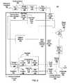
- FIG. 1is a block diagram of a system in accordance with an exemplary embodiment of the present disclosure
- FIG. 2is a diagrammatic representation of testing circuitry including distortion analysis circuitry in accordance with another exemplary embodiment of the present disclosure
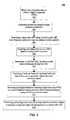
- FIG. 3is a flowchart of a method executed by the distortion analysis system of FIG. 1 ;
- FIG. 4is a diagrammatic representation of a fundamental and a harmonic direct digital synthesizer in accordance with yet another exemplary embodiment of the present disclosure.
- a direct digital synthesizermay be used to generate sinusoidal waveforms to a circuit-under-test (CUT) in real-time, in some cases allowing for the generation of a new sinusoidal waveform data point once every clock cycle.
- DDSdirect digital synthesizer
- CUTcircuit-under-test
- Some of the implementations described hereinutilize a 192 KHz clock, however other clock rates are also within the scope of the present disclosure.
- circuitrymay comprise, for example, singly or in any combination, hardwired circuitry, programmable circuitry, state machine circuitry, and/or firmware that stores instructions executed by programmable circuitry. It should be understood at the outset that any of the operations and/or operative components described in any embodiment or implementation herein may be implemented in software, firmware, hardwired circuitry and/or any combination thereof.
- testing circuitry 12may include a signal generator (not shown) that may be configured to apply a test signal 16 to circuitry under test 14 (CUT).
- the resulting output signali.e., signal under test 18
- test signal 16may typically be a distortion-free signal
- the distortion imparted by circuitry under test 14may be determined by comparing test signal 16 and signal under test 18 .
- circuitry under test 14may be driven by test signal 16 .
- test signal 16may include, but are not limited to, an 8 VAC peak-to-peak 1 kHz sinusoidal signal.
- the amplitude, frequency, and type of test signal (e.g., test signal 16 ) applied to circuitry under test 14may vary depending on the type of circuitry being tested (e.g., circuitry under test 14 ). For example, for some circuit types, a square wave signal or triangle wave signal may be applied to circuitry under test 14 . In some implementations, a sinusoidal wave signal may be provided to circuitry under test 14 as is discussed in further detail below.
- Testing circuitry 100may include a system clock generator 102 configured to receive a system reference frequency 104 .
- reference frequency 104may be a 10 MHz frequency, however, numerous other frequencies may be used without departing from the scope of the present disclosure.
- System clock generator 102may be configured to receive system reference frequency 104 at phase locked loop (PLL) 106 .
- PLL 106may generate an output signal dependent upon both the frequency and phase of system reference frequency 104 .
- This output signalmay be received by divider circuitry 108 before entering direct digital synthesizer (DDS) 110 .
- DDS 110may be configured to receive the output from divider circuitry and to generate an arbitrary waveform from this fixed frequency source. This waveform may be applied to PLL/multiplier 112 .
- DDS 110may include a number of different components, including, but not limited to, RAM, oscillator circuitry, counter circuitry, ADCs, DACs, etc.
- PLL/Multiplier 112may be configured to receive a signal of one frequency range (e.g., 12.5 MHz-25-MHz) and to increase the frequency by a given factor. For example, in this case, a 100 MHz-200 MHz frequency range may be generated if a multiplier of 8 is utilized.
- the output of PLL/Multiplier 112may be provided to multiplexer (MUX) circuitry 114 , which may be configured to provided the clock frequency to distortion analysis circuitry 116 .
- MUXmultiplexer
- distortion analysis circuitry 116may include a number of different components and may be implemented using a number of different implementations.
- distortion analysis circuitry 116may be implemented in a field programmable gate array (FPGA), System on a Chip (SoC), an application specific integrated circuit (ASIC), and/or any other type of semiconductor device.
- FPGAfield programmable gate array
- SoCSystem on a Chip
- ASICapplication specific integrated circuit
- Distortion analysis circuitry 116may be configured to receive the clock frequency output from MUX circuitry 114 at glitchless clock gate 118 .
- Glitchless clock gate 118may also be configured to receive a signal from synchronous bus interface 120 via logic 122 and to generate an output, which may be received by divider circuitry 124 .
- Divider circuitry 124may be configured to receive an input signal having a particular frequency (e.g. 122.88 MHz) and to generate an output frequency having a fraction of the input frequency (e.g. 12.288 MHz). This adjusted frequency signal may then be provided to both the fundamental direct digital synthesizer (DDS) 126 and the harmonic DDS 128 , which are each discussed in more detail below.
- DDSfundamental direct digital synthesizer
- fundamental DDS 126may include a variety of components, including, but not limited to, phase accumulator (PA) circuitry 130 and wave generation circuitry 132 .
- Fundamental DDS 126may be configured to provide adjustable frequency, phase, amplitude and offset capabilities.
- PA circuitry 130may be configured to generate a stream of phase numbers ( 204 ) for use by wave generation circuitry 132 .
- Wave generation circuitry 132may be configured to receive a clock frequency ( 202 ) at fundamental DDS 126 and to generate a digital sine wave using the adjusted clock frequency signal and the stream of phase numbers generated by PA circuitry 130 ( 206 ).
- Wave generation circuitry 132 and 140may be configured to implement a variety of different algorithms. Some of these algorithms may include, but are not limited to, Coordinate Rotation Digital Computer (CORDIC), sine-phase difference, modified Sunderland, Nicholas, and Taylor Series approximation algorithms. Of course, numerous other sine wave generation techniques may be employed without departing from the scope of the present disclosure.
- CORDICCoordinate Rotation Digital Computer
- sine-phase differencemodified Sunderland, Nicholas, and Taylor Series approximation algorithms.
- Taylor Series approximation algorithmsmay be employed without departing from the scope of the present disclosure.
- the 12.288 MHz clock frequency signalmay be used to drive wave generation circuitry 132 to produce a new digital serial word at the rate of 192 KS/s.
- the phase and amplitude valuesmay be selected.
- Wave generation circuitry 132may provide the digital serial data stream to audio digital-to-analog (DAC) converter 134 .
- DAC 134may then receive the digital sine wave ( 208 ) and may be configured to translate the serial data stream, e.g., digital sine wave, into an analog output waveform 136 that approximates a pure analog sine wave ( 210 ).
- Equation 1A refers to the amplitude of the sine wave that is programmed, Angle and Phase may be programmed values, and I is a number that may begin at 0 and may be incremented by 1 at every clock cycle of the 192 KHz clock.
- harmonic DDS 128may also include PA circuitry 138 and wave generation circuitry 140 .
- Harmonic DDS 128may be configured to cancel at least one harmonic associated with the digital sine wave to generate a digital distortion correction output ( 212 ).
- the digital distortion correction outputmay be provided to second DAC 142 to generate an analog distortion correction output 144 ( 214 ).
- Analog distortion correction output 144may be used to correct for distortion components in DAC 134 .
- the analog output waveform generated by DAC 134may be combined with the analog distortion correction output to generate a composite output 146 for transmission to a circuit-under-test ( 216 ) such as that shown in FIG. 1 .
- harmonic DDS 128may be configured to cancel up to 8 harmonics generated by first audio DAC 134 by analyzing the inherent non-linearities in first audio DAC 134 .
- composite output 146may be used to drive an ADC circuit under test CUT, such as CUT 14 shown in FIG. 1 , to test the CUT.
- composite output 146may be used to null a DAC CUT output to generate a null which may be used to evaluate the CUT performance.
- composite output waveform 146may be provided to notch filter circuitry 160 .
- Notch filter circuitry 160may be configured to receive the composite output waveform 146 and to filter composite output 146 to generate a filtered composite output. Filtered composite output may then be provided to differential amplifier 150 , which may amplify a difference between the filtered composite output waveform and a signal from the circuit-under-test to generate an amplified analog signal. Amplified analog signal may be converted to an amplified digital signal using ADC/DAC circuitry 152 . The amplified digital signal may be stored in capture memory 156 .
- a calibration sequencemay be generated for notch filter circuitry 160 .
- the calibration sequencemay be configured to calculate at least one of a harmonic amplitude and a harmonic phase corresponding to a measured unknown harmonic signal.
- frequenciesmay be generated by audio DAC 134 at the various expected harmonics and the phase and amplitude response of notch filter circuitry 160 may be measured.
- Calibration factorsmay be generated and used to calculate what harmonic amplitude and phase is present when an unknown harmonic is measured.
- a compensating distortion correction signalmay be generated to subtract the spurious frequency components. It should be noted that, in some instances, only the frequencies having corresponding notch filters may be tested with some of the algorithms described herein.
- composite output 146 and signal under test 148may be provided to differential amplifier circuitry 150 .
- Differential amplifier circuitry 150may be configured to generate a differential amplifier output using composite output signal 146 and signal under test 148 .
- the output of differential amplifiermay be provided to ADC/DAC circuitry 152 , which may be configured to- provide analog-to-digital- conversion and to provide a signal back to distortion analysis circuitry 116 .
- ADC/DAC interface circuitry 154may receive this converted signal from ADCIDAC circuitry 152 , provide any necessary conversion, and generate an output that may be received by capture memory 156 .
- the term “memory” as described herein,may refer to semiconductor firmware memory, programmable memory, non-volatile memory, read only memory, electrically programmable memory, random access memory, flash memory, magnetic disk memory, and/or optical disk memory.
- Fundamental DDS 302may be configured to receive numerous inputs relating to, for example, the angle, clock and the starting phase information. Of course, additional information may also be provided.
- first adder circuitry 306working in conjunction with second adder circuitry 308 , may be configured to receive the clock frequency ⁇ as well as the phase shift data ⁇ , perform an addition operation, and to provide the result to wave generation circuitry 310 .
- wave generation circuitry 310may then generate a digital sinusoidal waveform using this data resulting in a digital waveform of the equation Sine( ⁇ (n)+ ⁇ ).
- This digital waveformmay then be provided to multiplier 312 , which may perform a multiplication operation on the digital waveform and amplitude input A resulting in an output corresponding to the equation A*Sine( ⁇ (n)+ ⁇ ).
- This outputmay then be combined with a DC offset at third adder 314 to generate the digital sine wave or wave fundamental of the form A*Sine( ⁇ (n)+ ⁇ )+D.
- This signalmay then be provided to the first audio DAC 134 shown in FIG. 2 for conversion to an analog waveform.
- Harmonic DDS 304may be of a similar configuration and, as such, may also include first and second adder circuitry 316 and 318 , wave generation circuitry 320 , multiplier 322 , and third adder 324 .
- harmonic DDS 304may be configured to generate a digital distortion correction output, which may be configured to cancel at least one harmonic generated by Fundamental DDS 302 .
- the digital distortion correction output of harmonic DDS 304may be provided to second audio DAC 142 to generate an analog distortion correction output.
- Analog output 136 from first DAC 134 and analog distortion correction output 144 from second audio DAC 142may be combined to generate a composite output 146 for transmission to a circuit-under-test as is described in further detail above.
- the direct digital synthesizers described hereinmay include a variety of registers (e.g., registers 131 and 139 shown in FIG. 2 ) and other circuitry components in order to generate the sinusoidal waveforms described herein.
- the methods described hereinmay be implemented inside an FPGA. As such, each of the direct digital synthesizers may be controlled in part by a series of registers described in more detail in Tables 1-6.
- Wave phase interval register Address0x18E, HYDRA_ACH_WAVE_INTVL_W1 Address: 0x18F, HYDRA_ACH_WAVE_INTVL_W0 31:16 15:0 Wave_intvl Position Signal Name Description R/W SW HW Bit [31:0] Wave_intvl Point at which setting RW 0x0 0x0 ⁇ * n to zero, e.g., phase is the initial phase shift
- the wave phase interval registermay be a 32 bit register, which may be treated as two 16 bit read/write registers for purposes of reading and writing. This register may be used to keep mathematical errors in the phase accumulator when the ⁇ step is repeatedly added causing drift in the frequency of the signals being generated by fundamental DDS 302 and/or harmonic DDS 304 .
- the wave phase interval registermay be set to the number of master clock cycles after which the phase accumulator circuitry 138 may be back to its initial phase. This information may be utilized inside the signal generator to re-initialize the phase accumulation process.
- the wave phase interval registermay be programmed in units of the 192 kHz sample rate. For merely exemplary purposes, two examples of what may be programmed into the wave phase interval register (assuming a clock rate of 192 kHz) are provided below.
- this registermay be programmed to 192. After 1 ms (192/192 kHz) the phase of the 1 kHz signal that is produced may be back to where it was initially.
- this registermay be programmed to 19200.
- the phase of the 1.01 kHz waveform(i.e., finishing its 101 th cycle) may be the same as it was when the signal generation process was initiated.
- these examplesare merely intended for exemplary purposes as numerous other configurations and inputs may be used.
- Wave DC Offset Register Address0x190, HYDRA_ACH_WAVE_DC_W1 Address: 0x191, HYDRA_ACH_WAVE_DC_W0 31:16 15:0 bit [31:7] Wave Dc Offset xxxx Position Signal Name Description R/W SW HW Bit [31:16] Wave_dc_w1 Bit 31:16 of the DC RW 0x0 0x0 component of the fundamental Bit [15:7] Wave_dc_w0 Bit 15:7 of the DC RW 0x0 0x0 component of the fundamental
- the wave sine index registermay be a 16 bit read/write register. This register may act as the index of the sine components, fundamental, and harmonics, in an arbitrary wave.
- Ais the amplitude or scale
- Dis the DC offset
- ⁇is the phase shift or phase 0
- ⁇is the angular frequency or step.
- the wave sine index registermay also be used as an index when addressing the angular frequency register, the phase shift register, the amplitude, and the phase interval register of each sine component.
- the registers described in TABLES 4-6may be duplicated once for the fundamental tone DDS (e.g., 126) as well as once more for the harmonic tone DDS (e.g., 128). In some implementations, in order to write to or read from any of the registers of the individual DDS's this register must first be set to point to the DDS prior to using the registers described in TABLES 4-6.
- the wave step registermay be a 48 bit register, which may be treated as three 16 bit read/write registers for purposes of reading and writing.
- this wave step registerwhich represents an angle between 0 and Pi may be added to the number already present in phase accumulator circuitry 138 to form new phase angle.
- the resultant phase angle valuewould be greater than Pi then as the step value is being added a value of two Pi may also be subtracted out. (The net effect being that only phase angle values between ⁇ Pi and +Pi may be produced by the phase accumulator stage). It should be noted that numerous alternate algorithms for operating the phase accumulator circuitry 138 are also possible.
- the wave step registermay include a binary point located four bits from the left between Bit[ 44 ] and Bit[ 43 ] of the register such that an angle of one radian (1.000) would be represented as 0 ⁇ 1000 — 0000 — 0000 with the lsb of the 48 bit register representing an angle of 2 ⁇ ( ⁇ 44) radians.
- Wave_phase Position Signal Name DescriptionR/W SW HW Bit [31:16] Wave_phase_w1 Bit 31:16 of the RW 0x0 0x0 phase shift Bit [15:0] Wave_phase_w0 Bit 15:0 of the RW 0x0 0x0 phase shift
- the wave phase shift registermay be a 32 bit register, which may be treated as two 16 bit read/write registers for purposes of reading and writing.
- the value of the wave phase shift registermay be added to the upper bits of the value of phase accumulator circuitry 138 to form a new phase shifted waveform angle.
- the range of this phase shifted waveform anglemay take on values between +Pi and ⁇ Pi.
- this 32 bit shifted waveform angle valuemay have a binary point four places from the left and hold numbers in a two's compliment form between 0 ⁇ 3243F6A8 (+Pi) and 0 ⁇ CDBC0958 ( ⁇ Pi). Relating this to the above description this shifted phase angle represents the term ( ⁇ n+ ⁇ ).
- Wave generation circuitry 132 and 140may be used to either calculate or lookup the sin( ) value corresponding to the phase shifted angle value. This may be done in any number of ways ranging from a brute force lookup table (of depth 2 ⁇ 32) to a nearly all math CORDIC technique.
- the DC offsetmay be added to the scaled fundamental test tone term A ⁇ Sine ( ⁇ n+ ⁇ ) +D using 3rd adder 314 shown in FIG. 4 .
- the DC offsetmay be added to fundamental analog output 136 or the harmonic correction analog output 144 .
- Embodiments of the implementations described abovemay be implemented in a computer program that may be stored on a storage medium having instructions to program a system to perform the methods.
- the storage mediummay include, but is not limited to, any type of disk including floppy disks, optical disks, compact disk read-only memories (CD-ROMs), compact disk rewritables (CD-RWs), and magneto-optical disks, semiconductor devices such as read-only memories (ROMs), random access memories (RAMs) such as dynamic and static RAMs, erasable programmable read-only memories (EPROMs), electrically erasable programmable read-only memories (EEPROMs), flash memories, magnetic or optical cards, or any type of media suitable for storing electronic instructions.
- Other embodimentsmay be implemented as software modules executed by a programmable control device.
Landscapes
- Physics & Mathematics (AREA)
- General Physics & Mathematics (AREA)
- Engineering & Computer Science (AREA)
- General Engineering & Computer Science (AREA)
- Nonlinear Science (AREA)
- Mathematical Physics (AREA)
- Tests Of Electronic Circuits (AREA)
- Preparation Of Compounds By Using Micro-Organisms (AREA)
- Peptides Or Proteins (AREA)
Abstract
Description
N=A*sin(Angle*I+Phase) Equation (1)
| TABLE 1 |
| Wave phase interval register |
| Address: 0x18E, HYDRA_ACH_WAVE_INTVL_W1 |
| Address: 0x18F, HYDRA_ACH_WAVE_INTVL_W0 |
| 31:16 | 15:0 | |
| Wave_intvl |
| Position | Signal Name | Description | R/W | SW | HW |
| Bit [31:0] | Wave_intvl | Point at which setting | RW | 0x0 | 0x0 |
| ω * n to zero, e.g., | |||||
| phase is the initial | |||||
| phase shift | |||||
| TABLE 2 |
| Wave DC Offset Register |
| Address: 0x190, HYDRA_ACH_WAVE_DC_W1 |
| Address: 0x191, HYDRA_ACH_WAVE_DC_W0 |
| 31:16 | 15:0 |
| bit [31:7] Wave Dc Offset | xxxx |
| Position | Signal Name | Description | R/W | SW | HW |
| Bit [31:16] | Wave_dc_w1 | Bit 31:16 of the DC | RW | 0x0 | 0x0 |
| component of the | |||||
| fundamental | |||||
| Bit [15:7] | Wave_dc_w0 | Bit 15:7 of the DC | RW | 0x0 | 0x0 |
| component of the | |||||
| fundamental | |||||
| TABLE 3 |
| Wave Sine Index Register |
| Address: 0x193, HYDRA_ACH_WAVE_SINE_INDEX |
| 15 | 14 | 13 | 12 | 11 | 10 | 9 | 8 | 7 | 6 | 5 | 4 | 3 | 2 | 1 | 0 |
| W0 | sine_index | ||||||||
| Position | Signal Name | Description | R/W | SW | HW |
| Bit [4] | W0 | Write enable for bit 3:0 | R = 0 | 0x0 | 0x0 |
| Bits [3:0] | Sine_index | 0001: fundamental | RW | 0x0 | 0x0 |
| 0010: 2ndharmonic | |||||
| 0011: 3rdharmonic | |||||
| 0100: 4thharmonic | |||||
| 0101: 5thharmonic | |||||
| 0110: 6thharmonic | |||||
| 0111: 7thharmonic | |||||
| 1000: 8thharmonic | |||||
| 1001: 9thharmonic | |||||
| 1010: 10thharmonic | |||||
| TABLE 4 |
| Wave Step Register |
| Address: 0x194, HYDRA_ACH_WAVE_STEP_W2 |
| Address: 0x195, HYDRA_ACH_WAVE_STEP_W1 |
| Address: 0x196, HYDRA_ACH_WAVE_STEP_W0 |
| 47:32 | 31:16 | 15:0 |
| Wave_step |
| Position | Signal Name | Description | R/W | SW | HW |
| Bit [47:32] | Wave_step_w2 | Bit 48:32 of the | RW | 0x0 | 0x0 |
| angular frequency | |||||
| Bit [31:16] | Wave_step_w1 | Bit 31:16 of the | RW | 0x0 | 0x0 |
| angular frequency | |||||
| Bit [15:0] | Wave_step_w0 | Bit 15:0 of the | RW | 0x0 | 0x0 |
| angular frequency | |||||
| TABLE 5 |
| Wave Phase Shift Register |
| Address: 0x198, HYDRA_ACH_WAVE_PHASE_W1 |
| Address: 0x199, HYDRA_ACH_WAVE_PHASE_W0 |
| 31:16 | 15:0 | |
| Wave_phase |
| Position | Signal Name | Description | R/W | SW | HW |
| Bit [31:16] | Wave_phase_w1 | Bit 31:16 of the | RW | 0x0 | 0x0 |
| phase shift | |||||
| Bit [15:0] | Wave_phase_w0 | Bit 15:0 of the | RW | 0x0 | 0x0 |
| phase shift | |||||
| TABLE 6 |
| Wave Scale Register |
| Address: 0x19A, HYDRA_ACH_WAVE_SCALE_W1 |
| Address: 0x19B, HYDRA_ACH_WAVE_SCALE_W0 |
| 31:16 | 15:0 |
| Bit [31:7] Wave_scale | Xxxx |
| Position | Signal Name | Description | R/W | SW | HW |
| Bit [31:16] | Wave_scale_w1 | Bit 31:16 of the | RW | 0x0 | 0x0 |
| amplitude | |||||
| Bit [15:7] | Wave_scale_w0 | Bit 15:7 of the | RW | 0x0 | 0x0 |
| amplitude | |||||
Claims (17)
Priority Applications (1)
| Application Number | Priority Date | Filing Date | Title |
|---|---|---|---|
| US12/170,334US8239434B2 (en) | 2007-07-09 | 2008-07-09 | System, method, and apparatus for distortion analysis |
Applications Claiming Priority (2)
| Application Number | Priority Date | Filing Date | Title |
|---|---|---|---|
| US94857707P | 2007-07-09 | 2007-07-09 | |
| US12/170,334US8239434B2 (en) | 2007-07-09 | 2008-07-09 | System, method, and apparatus for distortion analysis |
Publications (2)
| Publication Number | Publication Date |
|---|---|
| US20090063071A1 US20090063071A1 (en) | 2009-03-05 |
| US8239434B2true US8239434B2 (en) | 2012-08-07 |
Family
ID=40337516
Family Applications (3)
| Application Number | Title | Priority Date | Filing Date |
|---|---|---|---|
| US12/170,334Active2031-06-07US8239434B2 (en) | 2007-07-09 | 2008-07-09 | System, method, and apparatus for distortion analysis |
| US12/170,401Active2030-07-30US8269480B2 (en) | 2007-07-09 | 2008-07-09 | Method and apparatus for identifying and reducing spurious frequency components |
| US13/090,560ActiveUS8415941B2 (en) | 2007-07-09 | 2011-04-20 | Method and apparatus for identifying and reducing spurious frequency components |
Family Applications After (2)
| Application Number | Title | Priority Date | Filing Date |
|---|---|---|---|
| US12/170,401Active2030-07-30US8269480B2 (en) | 2007-07-09 | 2008-07-09 | Method and apparatus for identifying and reducing spurious frequency components |
| US13/090,560ActiveUS8415941B2 (en) | 2007-07-09 | 2011-04-20 | Method and apparatus for identifying and reducing spurious frequency components |
Country Status (2)
| Country | Link |
|---|---|
| US (3) | US8239434B2 (en) |
| AR (1) | AR067500A1 (en) |
Families Citing this family (14)
| Publication number | Priority date | Publication date | Assignee | Title |
|---|---|---|---|---|
| US8239434B2 (en)* | 2007-07-09 | 2012-08-07 | Ltx Corporation | System, method, and apparatus for distortion analysis |
| US8867561B2 (en)* | 2010-05-10 | 2014-10-21 | Comcast Cable Communications, Llc | Managing upstream transmission in a network |
| US8605846B2 (en)* | 2010-12-17 | 2013-12-10 | Maxim Integrated Products, Inc. | Adaptive frequency synthesis for a serial data interface |
| US8405383B2 (en)* | 2011-03-14 | 2013-03-26 | General Electric Company | Three-phase selectable energy meter |
| US9998042B2 (en)* | 2013-03-04 | 2018-06-12 | Seagate Technology Llc | Torque disturbance cancellation for a motor |
| EP2816557B1 (en)* | 2013-06-20 | 2015-11-04 | Harman Becker Automotive Systems GmbH | Identifying spurious signals in audio signals |
| US9356578B1 (en) | 2014-12-10 | 2016-05-31 | Honeywell International Inc. | Spurious frequency attenuation servo without tuning filter |
| US10317514B2 (en) | 2015-08-11 | 2019-06-11 | Raytheon Company | Programmable apparatus for synthesized filter notch |
| US9973360B2 (en)* | 2015-12-18 | 2018-05-15 | Nxp Usa, Inc. | Method and apparatus for generating phase shift control signals |
| US9577657B1 (en) | 2016-05-02 | 2017-02-21 | Analog Devices, Inc. | Delta sigma patterns for calibrating a digital-to-analog converter |
| US10200222B2 (en) | 2017-01-31 | 2019-02-05 | Raytheon Company | Low cost and low frequency baseband two-tone test set using direct digital synthesizers as signal generators and a fully differential amplifier as the power combiner |
| US10374675B1 (en)* | 2018-03-06 | 2019-08-06 | Raytheon Company | Direct digital synthesis based phase shift digital beam forming |
| US12401371B2 (en) | 2022-02-28 | 2025-08-26 | Analog Devices, Inc. | Calibration of digital-to-analog converters |
| CN115589208B (en)* | 2022-10-31 | 2023-11-14 | 中国科学院高能物理研究所 | Magnetic alloy cavity harmonic compensation control method and related equipment |
Citations (24)
| Publication number | Priority date | Publication date | Assignee | Title |
|---|---|---|---|---|
| US5436600A (en) | 1994-07-29 | 1995-07-25 | The Regents Of The University Of California | MRI multi-frequency DSB and SSB RF synthesizer |
| US5687735A (en) | 1996-03-28 | 1997-11-18 | Hewlett-Packard Company | Robust time-diversity filter and method for removing electromagnetic interference |
| US5784413A (en) | 1996-09-06 | 1998-07-21 | General Instrument Corporation | Direct digital synthesis frequency-agile QPSK modulator |
| US5898325A (en)* | 1997-07-17 | 1999-04-27 | Analog Devices, Inc. | Dual tunable direct digital synthesizer with a frequency programmable clock and method of tuning |
| US6236267B1 (en) | 1998-12-29 | 2001-05-22 | International Business Machines Corporation | Linearization for power amplifiers using feed-forward and feedback control |
| US6744261B2 (en) | 2001-04-02 | 2004-06-01 | Agilent Technologies, Inc. | Method and an apparatus for measuring the ratio of the amplification factor of a signal level normalizer |
| US6825729B2 (en) | 2000-04-19 | 2004-11-30 | Siemens Aktiengesellschaft | Frequency synthesizer with sigma-delta modulation |
| US20040260506A1 (en) | 2000-11-15 | 2004-12-23 | Jones Aled Wynne | Tag tracking |
| US6867642B1 (en) | 2003-08-25 | 2005-03-15 | Lockheed Martin Corporation | Realtime adaptive notch compensator |
| US20050063553A1 (en) | 2003-08-01 | 2005-03-24 | Kazuhiko Ozawa | Microphone apparatus, noise reduction method and recording apparatus |
| US20050129139A1 (en) | 2003-12-03 | 2005-06-16 | Jones Aled W. | Tag tracking |
| US6924711B2 (en) | 2002-06-07 | 2005-08-02 | Utstarcom, Inc. | Multimode modulator employing a phase lock loop for wireless communications |
| US7103622B1 (en)* | 2002-10-08 | 2006-09-05 | Analog Devices, Inc. | Direct digital synthesizer with output signal jitter reduction |
| US7119553B2 (en) | 2003-06-11 | 2006-10-10 | Konsulteurope Limited Limited Joint Stock Company | Security scanners with capacitance and magnetic sensor arrays |
| US20070096759A1 (en)* | 2005-11-02 | 2007-05-03 | Chananiel Weinraub | Analog built-in self-test module |
| US20070192391A1 (en)* | 2006-02-10 | 2007-08-16 | Mcewan Thomas E | Direct digital synthesis radar timing system |
| US20070194986A1 (en) | 2006-02-21 | 2007-08-23 | Northrop Grumman Corporation | Wideband active phased array antenna system |
| US20070253561A1 (en) | 2006-04-27 | 2007-11-01 | Tsp Systems, Inc. | Systems and methods for audio enhancement |
| US20080063090A1 (en) | 2006-09-12 | 2008-03-13 | Xantech Corporation | System and method for automatic compensation of video signals |
| US7388497B1 (en) | 2003-09-17 | 2008-06-17 | The United States Of America As Represented By The Secretary Of The Navy | Radio frequency identification tag |
| US20090033375A1 (en)* | 2007-07-09 | 2009-02-05 | Solomon Max | Method and apparatus for identifying and reducing spurious frequency components |
| US20100036455A1 (en) | 2008-07-28 | 2010-02-11 | University Of Washington | Measurement and use of in-socket residual limb volume change data for prosthetic fitting |
| US20110043328A1 (en) | 2007-01-29 | 2011-02-24 | Fred Bassali | Advanced Vehicular Universal Transmitter Using Time Domain With Vehicle LocationLoggin System |
| US20110227767A1 (en)* | 2006-12-29 | 2011-09-22 | O'brien David | Compensating for harmonic distortion in an instrument channel |
- 2008
- 2008-07-09USUS12/170,334patent/US8239434B2/enactiveActive
- 2008-07-09USUS12/170,401patent/US8269480B2/enactiveActive
- 2008-07-10ARARP080102968Apatent/AR067500A1/enactiveIP Right Grant
- 2011
- 2011-04-20USUS13/090,560patent/US8415941B2/enactiveActive
Patent Citations (26)
| Publication number | Priority date | Publication date | Assignee | Title |
|---|---|---|---|---|
| US5436600A (en) | 1994-07-29 | 1995-07-25 | The Regents Of The University Of California | MRI multi-frequency DSB and SSB RF synthesizer |
| US5687735A (en) | 1996-03-28 | 1997-11-18 | Hewlett-Packard Company | Robust time-diversity filter and method for removing electromagnetic interference |
| US5784413A (en) | 1996-09-06 | 1998-07-21 | General Instrument Corporation | Direct digital synthesis frequency-agile QPSK modulator |
| US5898325A (en)* | 1997-07-17 | 1999-04-27 | Analog Devices, Inc. | Dual tunable direct digital synthesizer with a frequency programmable clock and method of tuning |
| US6236267B1 (en) | 1998-12-29 | 2001-05-22 | International Business Machines Corporation | Linearization for power amplifiers using feed-forward and feedback control |
| US6825729B2 (en) | 2000-04-19 | 2004-11-30 | Siemens Aktiengesellschaft | Frequency synthesizer with sigma-delta modulation |
| US20040260506A1 (en) | 2000-11-15 | 2004-12-23 | Jones Aled Wynne | Tag tracking |
| US6744261B2 (en) | 2001-04-02 | 2004-06-01 | Agilent Technologies, Inc. | Method and an apparatus for measuring the ratio of the amplification factor of a signal level normalizer |
| US6924711B2 (en) | 2002-06-07 | 2005-08-02 | Utstarcom, Inc. | Multimode modulator employing a phase lock loop for wireless communications |
| US7103622B1 (en)* | 2002-10-08 | 2006-09-05 | Analog Devices, Inc. | Direct digital synthesizer with output signal jitter reduction |
| US7295019B2 (en) | 2003-06-11 | 2007-11-13 | Konsulteurope Limited Limited Liability Joint Stock Company United Kingdon | Security scanners with capacitance and magnetic sensor arrays |
| US7119553B2 (en) | 2003-06-11 | 2006-10-10 | Konsulteurope Limited Limited Joint Stock Company | Security scanners with capacitance and magnetic sensor arrays |
| US20050063553A1 (en) | 2003-08-01 | 2005-03-24 | Kazuhiko Ozawa | Microphone apparatus, noise reduction method and recording apparatus |
| US6867642B1 (en) | 2003-08-25 | 2005-03-15 | Lockheed Martin Corporation | Realtime adaptive notch compensator |
| US7388497B1 (en) | 2003-09-17 | 2008-06-17 | The United States Of America As Represented By The Secretary Of The Navy | Radio frequency identification tag |
| US20050129139A1 (en) | 2003-12-03 | 2005-06-16 | Jones Aled W. | Tag tracking |
| US20070096759A1 (en)* | 2005-11-02 | 2007-05-03 | Chananiel Weinraub | Analog built-in self-test module |
| US20070192391A1 (en)* | 2006-02-10 | 2007-08-16 | Mcewan Thomas E | Direct digital synthesis radar timing system |
| US20070194986A1 (en) | 2006-02-21 | 2007-08-23 | Northrop Grumman Corporation | Wideband active phased array antenna system |
| US20070253561A1 (en) | 2006-04-27 | 2007-11-01 | Tsp Systems, Inc. | Systems and methods for audio enhancement |
| US20080063090A1 (en) | 2006-09-12 | 2008-03-13 | Xantech Corporation | System and method for automatic compensation of video signals |
| US20110227767A1 (en)* | 2006-12-29 | 2011-09-22 | O'brien David | Compensating for harmonic distortion in an instrument channel |
| US20110043328A1 (en) | 2007-01-29 | 2011-02-24 | Fred Bassali | Advanced Vehicular Universal Transmitter Using Time Domain With Vehicle LocationLoggin System |
| US20090033375A1 (en)* | 2007-07-09 | 2009-02-05 | Solomon Max | Method and apparatus for identifying and reducing spurious frequency components |
| US20110193547A1 (en)* | 2007-07-09 | 2011-08-11 | Ltx-Credence Corporation | Method and apparatus for identifying and reducing spurious frequency components |
| US20100036455A1 (en) | 2008-07-28 | 2010-02-11 | University Of Washington | Measurement and use of in-socket residual limb volume change data for prosthetic fitting |
Also Published As
| Publication number | Publication date |
|---|---|
| US20090063071A1 (en) | 2009-03-05 |
| US8415941B2 (en) | 2013-04-09 |
| US20090033375A1 (en) | 2009-02-05 |
| AR067500A1 (en) | 2009-10-14 |
| US8269480B2 (en) | 2012-09-18 |
| US20110193547A1 (en) | 2011-08-11 |
Similar Documents
| Publication | Publication Date | Title |
|---|---|---|
| US8239434B2 (en) | System, method, and apparatus for distortion analysis | |
| EP0451831B1 (en) | Low-distortion waveform generating method and waveform generator using the same | |
| EP2393224B1 (en) | Method and apparatus for synthesizing and correcting phase distortions in ultra-wide bandwidth optical waveforms | |
| US8400338B2 (en) | Compensating for harmonic distortion in an instrument channel | |
| CN101573592B (en) | Compensate for Harmonic Distortion in Instrument Channels | |
| US7890562B2 (en) | Sine wave generator with dual port look-up table | |
| CN100388156C (en) | Direct digital frequency synthesizer for cellular wireless communication systems based on fast frequency-hopped spread spectrum technology | |
| TWI423589B (en) | Apparatus for and method of generating a sinusoidal signal and method of manufacturing a semiconductor device | |
| US6911925B1 (en) | Linearity compensation by harmonic cancellation | |
| JP2009074941A (en) | Method and apparatus for measuring amplitude of periodic signal and magnetic head test method and apparatus | |
| Leitner et al. | Design techniques for direct digital synthesis circuits with improved frequency accuracy over wide frequency ranges | |
| JP2872275B2 (en) | Rf signal generation circuit arrangement for MR inspection | |
| CN112073064A (en) | Broadband signal generation device and method based on self-adaptive correction | |
| CN1790916B (en) | Calibration system for a linearity corrector using filter products | |
| Sodagar et al. | A novel architecture for ROM-less sine-output direct digital, frequency synthesizers by using the 2/sup nd/-order parabolic approximation | |
| US20140247049A1 (en) | Digital waveform synthesizer for nmr phase control | |
| JP2020148544A (en) | Phase noise measurement device and phase noise measurement method | |
| CN114710139A (en) | Harmonic extraction and synthesizer of APF control system | |
| JP5823785B2 (en) | Rotation angle detector | |
| JP3472333B2 (en) | Signal generator and distortion measuring device | |
| US12228429B2 (en) | Resolver-to-digital converter circuit, resolver signal processing apparatus, resolver signal processing method, and program | |
| Muñoz et al. | Digital Approaches on Frequency Tuning for Magnetoelectric Sensors | |
| JP4277205B2 (en) | Jitter generator | |
| KR20000031136A (en) | Direct digital frequency synthesizer | |
| US20010016863A1 (en) | Frequency synthesizer and gaussian noise generator using the same |
Legal Events
| Date | Code | Title | Description |
|---|---|---|---|
| AS | Assignment | Owner name:LTX CORPORATION, MASSACHUSETTS Free format text:ASSIGNMENT OF ASSIGNORS INTEREST;ASSIGNORS:MAX, SOLOMON;HANNAFORD, CHRISTOPHER JOEL;REEL/FRAME:021782/0460;SIGNING DATES FROM 20080924 TO 20081009 Owner name:LTX CORPORATION, MASSACHUSETTS Free format text:ASSIGNMENT OF ASSIGNORS INTEREST;ASSIGNORS:MAX, SOLOMON;HANNAFORD, CHRISTOPHER JOEL;SIGNING DATES FROM 20080924 TO 20081009;REEL/FRAME:021782/0460 | |
| AS | Assignment | Owner name:LTX-CREDENCE CORPORATION, MASSACHUSETTS Free format text:MERGER;ASSIGNOR:CREDENCE SYSTEMS CORPORATION;REEL/FRAME:025894/0629 Effective date:20090130 | |
| STCF | Information on status: patent grant | Free format text:PATENTED CASE | |
| AS | Assignment | Owner name:SILICON VALLEY BANK, AS ADMINISTRATIVE AGENT, CALI Free format text:SECURITY AGREEMENT;ASSIGNORS:LTX-CREDENCE CORPORATION;EVERETT CHARLES TECHNOLOGIES LLC;REEL/FRAME:032086/0476 Effective date:20131127 | |
| AS | Assignment | Owner name:XCERRA CORPORATION, MASSACHUSETTS Free format text:CHANGE OF NAME;ASSIGNOR:LTX-CREDENCE CORPORATION;REEL/FRAME:033032/0768 Effective date:20140520 | |
| AS | Assignment | Owner name:EVERETT CHARLES TECHNOLOGIES LLC, MASSACHUSETTS Free format text:RELEASE OF SECURITY INTEREST IN UNITED STATES PATENTS;ASSIGNOR:SILICON VALLEY BANK, AS ADMINISTRATIVE AGENT;REEL/FRAME:034660/0394 Effective date:20141215 Owner name:XCERRA CORPORATION, MASSACHUSETTS Free format text:RELEASE OF SECURITY INTEREST IN UNITED STATES PATENTS;ASSIGNOR:SILICON VALLEY BANK, AS ADMINISTRATIVE AGENT;REEL/FRAME:034660/0394 Effective date:20141215 Owner name:SILICON VALLEY BANK, AS ADMINISTRATIVE AGENT, CALI Free format text:SECURITY AGREEMENT;ASSIGNORS:XCERRA CORPORATION;EVERETT CHARLES TECHNOLOGIES LLC;REEL/FRAME:034660/0188 Effective date:20141215 | |
| FPAY | Fee payment | Year of fee payment:4 | |
| AS | Assignment | Owner name:SILICON VALLEY BANK, AS ADMINISTRATIVE AGENT, CALI Free format text:CORRECTIVE ASSIGNMENT TO CORRECT THE INCORRECT PATENT NUMBER 7261561 AND REPLACE WITH PATENT NUMBER 7231561 PREVIOUSLY RECORDED ON REEL 034660 FRAME 0188. ASSIGNOR(S) HEREBY CONFIRMS THE SECURITY AGREEMENT;ASSIGNORS:XCERRA CORPORATION;EVERETT CHARLES TECHNOLOGIES LLC;REEL/FRAME:037824/0372 Effective date:20141215 | |
| AS | Assignment | Owner name:DEUTSCHE BANK AG NEW YORK BRANCH, AS COLLATERAL AGENT, NEW YORK Free format text:PATENT SECURITY AGREEMENT;ASSIGNOR:XCERRA CORPORATION;REEL/FRAME:047185/0624 Effective date:20181001 Owner name:DEUTSCHE BANK AG NEW YORK BRANCH, AS COLLATERAL AG Free format text:PATENT SECURITY AGREEMENT;ASSIGNOR:XCERRA CORPORATION;REEL/FRAME:047185/0624 Effective date:20181001 | |
| AS | Assignment | Owner name:DEUTSCHE BANK AG NEW YORK BRANCH, AS COLLATERAL AGENT, NEW YORK Free format text:CORRECTIVE ASSIGNMENT TO CORRECT THE INCORRECT STATEMENT THAT THIS DOCUMENT SERVES AS AN OATH/DECLARATION PREVIOUSLY RECORDED ON REEL 047185 FRAME 0628. ASSIGNOR(S) HEREBY CONFIRMS THE PATENT SECURITY AGREEMENT;ASSIGNOR:XCERRA CORPORATION;REEL/FRAME:047675/0354 Effective date:20181001 Owner name:DEUTSCHE BANK AG NEW YORK BRANCH, AS COLLATERAL AG Free format text:CORRECTIVE ASSIGNMENT TO CORRECT THE INCORRECT STATEMENT THAT THIS DOCUMENT SERVES AS AN OATH/DECLARATION PREVIOUSLY RECORDED ON REEL 047185 FRAME 0628. ASSIGNOR(S) HEREBY CONFIRMS THE PATENT SECURITY AGREEMENT;ASSIGNOR:XCERRA CORPORATION;REEL/FRAME:047675/0354 Effective date:20181001 | |
| MAFP | Maintenance fee payment | Free format text:PAYMENT OF MAINTENANCE FEE, 8TH YEAR, LARGE ENTITY (ORIGINAL EVENT CODE: M1552); ENTITY STATUS OF PATENT OWNER: LARGE ENTITY Year of fee payment:8 | |
| MAFP | Maintenance fee payment | Free format text:PAYMENT OF MAINTENANCE FEE, 12TH YEAR, LARGE ENTITY (ORIGINAL EVENT CODE: M1553); ENTITY STATUS OF PATENT OWNER: LARGE ENTITY Year of fee payment:12 | |
| AS | Assignment | Owner name:XCERRA CORPORATION, MASSACHUSETTS Free format text:TERMINATION AND RELEASE OF SECURITY INTEREST IN PATENTS, RECORDED AT REEL 047185, FRAME 0624;ASSIGNOR:DEUTSCHE BANK AG NEW YORK BRANCH, AS AGENT;REEL/FRAME:066762/0811 Effective date:20240209 |