US8238842B2 - Method and system for an on-chip and/or an on-package transmit/receive switch and antenna - Google Patents
Method and system for an on-chip and/or an on-package transmit/receive switch and antennaDownload PDFInfo
- Publication number
- US8238842B2 US8238842B2US12/397,024US39702409AUS8238842B2US 8238842 B2US8238842 B2US 8238842B2US 39702409 AUS39702409 AUS 39702409AUS 8238842 B2US8238842 B2US 8238842B2
- Authority
- US
- United States
- Prior art keywords
- distributed antenna
- antenna
- switches
- lnas
- pas
- Prior art date
- Legal status (The legal status is an assumption and is not a legal conclusion. Google has not performed a legal analysis and makes no representation as to the accuracy of the status listed.)
- Active, expires
Links
- 238000000034methodMethods0.000titleclaimsabstractdescription24
- 230000008878couplingEffects0.000claimsabstractdescription11
- 238000010168coupling processMethods0.000claimsabstractdescription11
- 238000005859coupling reactionMethods0.000claimsabstractdescription11
- 238000004891communicationMethods0.000claimsdescription12
- 238000010586diagramMethods0.000description10
- 230000005540biological transmissionEffects0.000description9
- 230000005236sound signalEffects0.000description9
- 238000012545processingMethods0.000description7
- 238000004590computer programMethods0.000description5
- 230000009977dual effectEffects0.000description5
- 238000005070samplingMethods0.000description5
- 230000008569processEffects0.000description4
- 238000006243chemical reactionMethods0.000description3
- 230000003203everyday effectEffects0.000description3
- 230000006870functionEffects0.000description3
- 238000010295mobile communicationMethods0.000description3
- 238000012546transferMethods0.000description3
- 238000005516engineering processMethods0.000description2
- 238000001914filtrationMethods0.000description2
- 239000000463materialSubstances0.000description2
- 239000002184metalSubstances0.000description2
- 230000004044responseEffects0.000description2
- 238000013459approachMethods0.000description1
- 230000001413cellular effectEffects0.000description1
- 239000004020conductorSubstances0.000description1
- 238000011161developmentMethods0.000description1
- 230000000694effectsEffects0.000description1
- 239000004744fabricSubstances0.000description1
- 238000010348incorporationMethods0.000description1
- 230000010365information processingEffects0.000description1
- 239000011810insulating materialSubstances0.000description1
- 230000010354integrationEffects0.000description1
- 238000002955isolationMethods0.000description1
- 238000012986modificationMethods0.000description1
- 230000004048modificationEffects0.000description1
- 238000011160researchMethods0.000description1
- 230000008054signal transmissionEffects0.000description1
Images


Classifications
- H—ELECTRICITY
- H01—ELECTRIC ELEMENTS
- H01L—SEMICONDUCTOR DEVICES NOT COVERED BY CLASS H10
- H01L23/00—Details of semiconductor or other solid state devices
- H01L23/58—Structural electrical arrangements for semiconductor devices not otherwise provided for, e.g. in combination with batteries
- H01L23/64—Impedance arrangements
- H01L23/66—High-frequency adaptations
- H—ELECTRICITY
- H04—ELECTRIC COMMUNICATION TECHNIQUE
- H04B—TRANSMISSION
- H04B1/00—Details of transmission systems, not covered by a single one of groups H04B3/00 - H04B13/00; Details of transmission systems not characterised by the medium used for transmission
- H04B1/38—Transceivers, i.e. devices in which transmitter and receiver form a structural unit and in which at least one part is used for functions of transmitting and receiving
- H04B1/40—Circuits
- H04B1/44—Transmit/receive switching
- H04B1/48—Transmit/receive switching in circuits for connecting transmitter and receiver to a common transmission path, e.g. by energy of transmitter
- H—ELECTRICITY
- H01—ELECTRIC ELEMENTS
- H01Q—ANTENNAS, i.e. RADIO AERIALS
- H01Q3/00—Arrangements for changing or varying the orientation or the shape of the directional pattern of the waves radiated from an antenna or antenna system
- H01Q3/26—Arrangements for changing or varying the orientation or the shape of the directional pattern of the waves radiated from an antenna or antenna system varying the relative phase or relative amplitude of energisation between two or more active radiating elements; varying the distribution of energy across a radiating aperture
- H01Q3/30—Arrangements for changing or varying the orientation or the shape of the directional pattern of the waves radiated from an antenna or antenna system varying the relative phase or relative amplitude of energisation between two or more active radiating elements; varying the distribution of energy across a radiating aperture varying the relative phase between the radiating elements of an array
- H01Q3/34—Arrangements for changing or varying the orientation or the shape of the directional pattern of the waves radiated from an antenna or antenna system varying the relative phase or relative amplitude of energisation between two or more active radiating elements; varying the distribution of energy across a radiating aperture varying the relative phase between the radiating elements of an array by electrical means
- H—ELECTRICITY
- H01—ELECTRIC ELEMENTS
- H01L—SEMICONDUCTOR DEVICES NOT COVERED BY CLASS H10
- H01L2223/00—Details relating to semiconductor or other solid state devices covered by the group H01L23/00
- H01L2223/58—Structural electrical arrangements for semiconductor devices not otherwise provided for
- H01L2223/64—Impedance arrangements
- H01L2223/66—High-frequency adaptations
- H01L2223/6661—High-frequency adaptations for passive devices
- H01L2223/6677—High-frequency adaptations for passive devices for antenna, e.g. antenna included within housing of semiconductor device
- H—ELECTRICITY
- H01—ELECTRIC ELEMENTS
- H01L—SEMICONDUCTOR DEVICES NOT COVERED BY CLASS H10
- H01L2924/00—Indexing scheme for arrangements or methods for connecting or disconnecting semiconductor or solid-state bodies as covered by H01L24/00
- H01L2924/0001—Technical content checked by a classifier
- H01L2924/0002—Not covered by any one of groups H01L24/00, H01L24/00 and H01L2224/00
Definitions
- Certain embodiments of the inventionrelate to wireless communication. More specifically, certain embodiments of the invention relate to a method and system for an on-chip and/or on-package transmit/receive (T/R) switch and antenna.
- T/Rtransmit/receive
- Mobile communicationshave changed the way people communicate and mobile phones have been transformed from a luxury item to an essential part of every day life.
- the use of mobile phonesis today dictated by social situations, rather than hampered by location or technology.
- voice connectionsfulfill the basic need to communicate, and mobile voice connections continue to filter even further into the fabric of every day life, the mobile Internet is the next step in the mobile communication revolution.
- the mobile Internetis poised to become a common source of everyday information, and easy, versatile mobile access to this data will be taken for granted.
- a system and/or method for an on-chip and/or on-package transmit/receive switch and antennasubstantially as shown in and/or described in connection with at least one of the figures, as set forth more completely in the claims.
- FIG. 1is a block diagram of an exemplary wireless system, which may be utilized in accordance with an embodiment of the invention.
- FIG. 2is a block diagram illustrating an exemplary multi-port distributed antenna on a chip, in accordance with an embodiment of the invention.
- FIG. 3Ais a block diagram illustrating a plan view of exemplary transmit/receive switches and a multi-port distributed antenna on a chip, in accordance with an embodiment of the invention.
- FIG. 3Bis a block diagram illustrating a plan view of an exemplary transmit/receive switch and a multi-port distributed antenna on a chip in TDD mode, in accordance with an embodiment of the invention
- FIG. 4is a block diagram illustrating exemplary steps for implementing a transmit/receive switch and a multiport distributed antenna, in accordance with an embodiment of the invention.
- Certain aspects of the inventionmay be found in a method and system for an on-chip and/or on-package transmit/receive (T/R) switch and antenna.
- Exemplary aspects of the inventionmay comprise configuring one or more T/R switches, which may be integrated on a chip with a plurality of low noise amplifiers (LNAs) and a plurality of power amplifiers (PAs), to selectively couple one or more of the plurality of LNAs and/or one or more of the plurality of PAs to one or more of a plurality of ports of a multi-port distributed antenna.
- LNAslow noise amplifiers
- PAspower amplifiers
- the selectively coupled plurality of LNAs and PAsmay be impedance matched to the multi-port distributed antenna by coupling the one or more of the plurality of LNAs and PAs to the one or more of a plurality of ports based on a characteristic impedance of the multi-port distributed antenna at the one of a plurality of ports.
- the T/R switchwhich may comprise CMOS switches, may be integrated on a package, where the chip may be bonded to the package.
- the signals, which may comprise RF signals, transmitted and received by the multi-port distributed antennamay be time division duplexed.
- the multi-port distributed antennamay be integrated on a chip with the LNAs and PAs, or integrated on a package to which the chip is bonded.
- the multi-port distributed antennamay comprise a microstrip antenna.
- the one of the plurality of LNAs and the one of the plurality of PAsmay be coupled to different ports on the multi-port distributed antenna via the T/R switch.
- FIG. 1is a block diagram of an exemplary wireless system, which may be utilized in accordance with an embodiment of the invention.
- the wireless device 150may comprise an antenna 151 , a transceiver 152 , a baseband processor 154 , a processor 156 , a system memory 158 , a logic block 160 , a chip 162 , a distributed antenna 164 , transmit/receive (T/R) switches 165 , an external headset port 166 , and a package 167 .
- T/Rtransmit/receive
- the wireless device 150may also comprise an analog microphone 168 , integrated hands-free (IHF) stereo speakers 170 , a hearing aid compatible (HAC) coil 174 , a dual digital microphone 176 , a vibration transducer 178 , a keypad and/or touchscreen 180 , and a display 182 .
- IHFintegrated hands-free
- HAChearing aid compatible
- the transceiver 152may comprise suitable logic, circuitry, interface(s), and/or code that may be enabled to modulate and upconvert baseband signals to RF signals for transmission by one or more antennas, which may be represented generically by the antenna 151 .
- the transceiver 152may also be enabled to downconvert and demodulate received RF signals to baseband signals.
- the RF signalsmay be received by one or more antennas, which may be represented generically by the antenna 151 , or the distributed antenna 164 . Different wireless systems may use different antennas for transmission and reception.
- the transceiver 152may be enabled to execute other functions, for example, filtering the baseband and/or RF signals, and/or amplifying the baseband and/or RF signals.
- the transceiver 152may be implemented as a separate transmitter and a separate receiver.
- the plurality of transceivers, transmitters and/or receiversmay enable the wireless device 150 to handle a plurality of wireless protocols and/or standards including cellular, WLAN and PAN.
- Wireless technologies handled by the wireless device 150may comprise GSM, CDMA, CDMA2000, WCDMA, GMS, GPRS, EDGE, WIMAX, WLAN, 3GPP, UMTS, BLUETOOTH, and ZIGBEE, for example.
- the baseband processor 154may comprise suitable logic, circuitry, interface(s), and/or code that may be enabled to process baseband signals for transmission via the transceiver 152 and/or the baseband signals received from the transceiver 152 .
- the processor 156may be any suitable processor or controller such as a CPU, DSP, ARM, or any type of integrated circuit processor.
- the processor 156may comprise suitable logic, circuitry, and/or code that may be enabled to control the operations of the transceiver 152 and/or the baseband processor 154 .
- the processor 156may be utilized to update and/or modify programmable parameters and/or values in a plurality of components, devices, and/or processing elements in the transceiver 152 and/or the baseband processor 154 . At least a portion of the programmable parameters may be stored in the system memory 158 .
- Control and/or data informationwhich may comprise the programmable parameters, may be transferred from other portions of the wireless device 150 , not shown in FIG. 1 , to the processor 156 .
- the processor 156may be enabled to transfer control and/or data information, which may include the programmable parameters, to other portions of the wireless device 150 , not shown in FIG. 1 , which may be part of the wireless device 150 .
- the processor 156may utilize the received control and/or data information, which may comprise the programmable parameters, to determine an operating mode of the transceiver 152 .
- the processor 156may be utilized to select a specific frequency for a local oscillator, a specific gain for a variable gain amplifier, configure the local oscillator and/or configure the variable gain amplifier for operation in accordance with various embodiments of the invention.
- the specific frequency selected and/or parameters needed to calculate the specific frequency, and/or the specific gain value and/or the parameters, which may be utilized to calculate the specific gainmay be stored in the system memory 158 via the processor 156 , for example.
- the information stored in system memory 158may be transferred to the transceiver 152 from the system memory 158 via the processor 156 .
- the system memory 158may comprise suitable logic, circuitry, interface(s), and/or code that may be enabled to store a plurality of control and/or data information, including parameters needed to calculate frequencies and/or gain, and/or the frequency value and/or gain value.
- the system memory 158may store at least a portion of the programmable parameters that may be manipulated by the processor 156 .
- the logic block 160may comprise suitable logic, circuitry, interface(s), and/or code that may enable controlling of various functionalities of the wireless device 150 .
- the logic block 160may comprise one or more state machines that may generate signals to control the transceiver 152 and/or the baseband processor 154 .
- the logic block 160may also comprise registers that may hold data for controlling, for example, the transceiver 152 and/or the baseband processor 154 .
- the logic block 160may also generate and/or store status information that may be read by, for example, the processor 156 .
- Amplifier gains and/or filtering characteristics, for example,may be controlled by the logic block 160 .
- the BT radio/processor 163may comprise suitable circuitry, logic, interface(s), and/or code that may enable transmission and reception of Bluetooth signals.
- the BT radio/processor 163may enable processing and/or handling of BT baseband signals.
- the BT radio/processor 163may process or handle BT signals received and/or BT signals transmitted via a wireless communication medium.
- the BT radio/processor 163may also provide control and/or feedback information to/from the baseband processor 154 and/or the processor 156 , based on information from the processed BT signals.
- the BT radio/processor 163may communicate information and/or data from the processed BT signals to the processor 156 and/or to the system memory 158 .
- the BT radio/processor 163may receive information from the processor 156 and/or the system memory 158 , which may be processed and transmitted via the wireless communication medium a Bluetooth headset, for example
- the CODEC 172may comprise suitable circuitry, logic, interface(s), and/or code that may process audio signals received from and/or communicated to input/output devices.
- the input devicesmay be within or communicatively coupled to the wireless device 150 , and may comprise the analog microphone 168 , the stereo speakers 170 , the hearing aid compatible (HAC) coil 174 , the dual digital microphone 176 , and the vibration transducer 178 , for example.
- the CODEC 172may be operable to up-convert and/or down-convert signal frequencies to desired frequencies for processing and/or transmission via an output device.
- the CODEC 172may enable utilizing a plurality of digital audio inputs, such as 16 or 18-bit inputs, for example.
- the CODEC 172may also enable utilizing a plurality of data sampling rate inputs.
- the CODEC 172may accept digital audio signals at sampling rates such as 8 kHz, 11.025 kHz, 12 kHz, 16 kHz, 22.05 kHz, 24 kHz, 32 kHz, 44.1 kHz, and/or 48 kHz.
- the CODEC 172may also support mixing of a plurality of audio sources.
- the CODEC 172may support audio sources such as general audio, polyphonic ringer, I 2 S FM audio, vibration driving signals, and voice.
- the general audio and polyphonic ringer sourcesmay support the plurality of sampling rates that the audio CODEC 172 is enabled to accept, while the voice source may support a portion of the plurality of sampling rates, such as 8 kHz and 16 kHz, for example.
- the CODEC 172may utilize a programmable infinite impulse response (IIR) filter and/or a programmable finite impulse response (FIR) filter for at least a portion of the audio sources to compensate for passband amplitude and phase fluctuation for different output devices.
- filter coefficientsmay be configured or programmed dynamically based on current operations. Moreover, the filter coefficients may be switched in one-shot or may be switched sequentially, for example.
- the CODEC 172may also utilize a modulator, such as a Delta-Sigma ( ⁇ - ⁇ ) modulator, for example, to code digital output signals for analog processing.
- ⁇ - ⁇Delta-Sigma
- the chip 162may comprise an integrated circuit with multiple functional blocks integrated within, such as the transceiver 152 , the processor 156 , the baseband processor 154 , the BT radio/processor 163 , the T/R switches 165 , the CODEC 172 , and the distributed antenna 164 .
- the number of functional blocks integrated in the chip 162is not limited to the number shown in FIG. 1 . Accordingly, any number of blocks may be integrated on the chip 162 depending on chip space and wireless device 150 requirements, for example.
- the distributed antenna 164may comprise a plurality of ports for coupling signals in and/or out of the distributed antenna 164 , and may be integrated in and/or on the chip 162 .
- the physical dimensions of the distributed antenna 164may be configured to optimize a frequency of operation and/or characteristic impedance at the plurality of ports.
- the distributed antenna 164may be integrated on a package to which the chip 162 may be affixed. In this manner, the dimensions of the distributed antenna 164 may not be limited by the size of the chip 162 .
- the T/R switches 165may comprise suitable circuitry, logic, interface(s), and/or code that may be operable to switch multiple components in the transceiver 152 to ports on the distributed antenna 164 .
- the T/R switches 165may comprise a plurality of switches that may enable the coupling of multiple devices to a single port on the distributed antenna 164 .
- an LNA and a PA in the transceiver 152may share a single port in the distributed antenna 164 , and may be operated in time division duplex (TDD) mode utilizing the T/R switches 165 , which may alternate between coupling the LNA and the PA to a port on the distributed antenna 164 .
- TDDtime division duplex
- the portmay be selected based on impedance matching between the port and the output impedance of the PA and input impedance of the LNA, for example.
- the T/R switches 165may comprise a plurality of CMOS switches, for example, that may be enabled by the processor 156 or other control circuitry in the wireless device 150 .
- the external headset port 166may comprise a physical connection for an external headset to be communicatively coupled to the wireless device 150 .
- the analog microphone 168may comprise suitable circuitry, logic, interface(s), and/or code that may detect sound waves and convert them to electrical signals via a piezoelectric effect, for example.
- the electrical signals generated by the analog microphone 168may comprise analog signals that may require analog to digital conversion before processing.
- the package 167may comprise a printed circuit board or other support structure for the chip 162 and other components of the wireless device 150 .
- the chip 162may be bonded to the package 167 .
- the package 167may comprise insulating and conductive material, for example, and may provide isolation between electrical components mounted on the package 167 .
- the stereo speakers 170may comprise a pair of speakers that may be operable to generate audio signals from electrical signals received from the CODEC 172 .
- the HAC coil 174may comprise suitable circuitry, logic, and/or code that may enable communication between the wireless device 150 and a T-coil in a hearing aid, for example. In this manner, electrical audio signals may be communicated to a user that utilizes a hearing aid, without the need for generating sound signals via a speaker, such as the stereo speakers 170 , and converting the generated sound signals back to electrical signals in a hearing aid, and subsequently back into amplified sound signals in the user's ear, for example.
- the dual digital microphone 176may comprise suitable circuitry, logic, interface(s), and/or code that may be operable to detect sound waves and convert them to electrical signals.
- the electrical signals generated by the dual digital microphone 176may comprise digital signals, and thus may not require analog to digital conversion prior to digital processing in the CODEC 172 .
- the dual digital microphone 176may enable beamforming capabilities, for example.
- the vibration transducer 178may comprise suitable circuitry, logic, interface(s), and/or code that may enable notification of an incoming call, alerts and/or message to the wireless device 150 without the use of sound.
- the vibration transducermay generate vibrations that may be in synch with, for example, audio signals such as speech or music.
- control and/or data informationwhich may comprise the programmable parameters, may be transferred from other portions of the wireless device 150 , not shown in FIG. 1 , to the processor 156 .
- the processor 156may be enabled to transfer control and/or data information, which may include the programmable parameters, to other portions of the wireless device 150 , not shown in FIG. 1 , which may be part of the wireless device 150 .
- the processor 156may utilize the received control and/or data information, which may comprise the programmable parameters, to determine an operating mode of the transceiver 152 .
- the processor 156may be utilized to select a specific frequency for a local oscillator, a specific gain for a variable gain amplifier, configure the local oscillator and/or configure the variable gain amplifier for operation in accordance with various embodiments of the invention.
- the specific frequency selected and/or parameters needed to calculate the specific frequency, and/or the specific gain value and/or the parameters, which may be utilized to calculate the specific gainmay be stored in the system memory 158 via the processor 156 , for example.
- the information stored in system memory 158may be transferred to the transceiver 152 from the system memory 158 via the processor 156 .
- the CODEC 172 in the wireless device 150may communicate with the processor 156 in order to transfer audio data and control signals.
- Control registers for the CODEC 172may reside within the processor 156 .
- the processor 156may exchange audio signals and control information via the system memory 158 .
- the CODEC 172may up-convert and/or down-convert the frequencies of multiple audio sources for processing at a desired sampling rate.
- the wireless signalsmay be transmitted and received by the distributed antenna 164 which may comprise a plurality of input/output ports.
- the characteristic impedance seen by a device coupled to a particular portmay be configured by the physical dimensions and by which of the plurality of ports the device may be coupled to, for example.
- power amplifiers and/or low noise amplifiers with similar impedancesmay be coupled to the same port on the distributed antenna 164 . This may be accomplished with the T/R switches 165 , which may couple an LNA and a PA to the same port on the distributed antenna 164 , but at alternate times, thus operating in TDD mode. Sharing ports on the distributed antenna 164 for both transmission and reception of signals may reduce space requirements on the chip 162 .
- the distributed antennamay be integrated on the package 167 , reducing space requirements of the chip 162 and improving space utilization in the wireless device 150 .
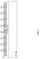
- FIG. 2is a block diagram illustrating an exemplary multi-port distributed antenna on a chip, in accordance with an embodiment of the invention.
- the chip 162there is shown the chip 162 , a distributed antenna 201 , IC circuitry 203 , and antenna ports 205 A- 205 H.
- the chip 162may be as described with respect to FIG. 1 .
- the IC circuitry 203may comprise devices integrated in the chip 162 , such as the transceiver 152 , the processor 156 , the T/R switches 165 , and the baseband processor 154 , for example.
- the distributed antenna 201may comprise an antenna integrated in and/or on the chip 162 that may comprise a plurality of ports, the antenna ports 205 A- 205 H, such that driver and receiver circuitry may be coupled to appropriate points along the distributed antenna 201 .
- LNAsmay be coupled to ports that exhibit high characteristic impedance
- PAsmay be coupled to ports that exhibit low characteristic impedance.
- the distributed antenna 201may comprise a microstrip or coplanar waveguide, for example.
- the antenna ports 205 A- 205 Hmay comprise electrical contacts along the length of the distributed antenna 201 that may enable coupling to the antenna at a plurality of points. In this manner, devices may be coupled to the distributed antenna 201 where the characteristic impedance may be matched to the desirable impedance for the device to be coupled.
- the antenna ports 205 A- 205 Hmay comprise metal strips, for example, that may be electrically coupled to the distributed antenna 201 .
- the antenna ports 205 A- 205 Hmay be coupled to T/R switches such as the T/R switches 165 , described with respect to FIG. 1 .
- a plurality of PAs and LNAsmay be coupled to the antenna ports 205 A- 205 H via a T/R switch comprising an array of switches to allow multiple devices to be coupled to a single antenna port 205 A- 205 H.
- the impedance of the devices to be coupledmay be matched to the characteristic impedance of the port to be coupled to such that the efficiency of the transmission of signals is maximized. This may, for example, increase the efficiency and thus the battery life of the wireless device 150 .
- FIG. 3Ais a block diagram illustrating a plan view of exemplary transmit/receive switches and a multi-port distributed antenna on a chip, in accordance with an embodiment of the invention.
- the chip 162there is shown the chip 162 , the distributed antenna 201 , the antenna ports 205 A- 205 H, baseband/RF circuitry 301 , amplifiers 303 A- 303 H, and T/R switches 310 .
- the baseband/RF circuitry 301may comprise suitable, circuitry, logic, interface(s), and/or code that may be operable to process baseband and RF signals.
- the baseband/RF circuitry 301may comprise the transceiver 152 , the baseband processor 154 , the processor 156 , the CODEC 172 , and the BT radio/processor 163 , for example, described with respect to FIG. 1 . Accordingly, the baseband/RF circuitry 301 may generate signals to be communicated to one or more of the amplifiers 303 A- 303 H, and may receive signals generated by one or more of the amplifiers 303 A- 303 H.
- the amplifiers 303 A- 303 Hmay comprise suitable, circuitry, logic, interface(s), and/or code that may be operable to amplify received signals, and may comprise power amplifiers (PAs) and/or low noise amplifiers (LNAs) that may be operable to communicate signals to and from the wireless medium via the distributed antenna 201 .
- PAspower amplifiers
- LNAslow noise amplifiers
- the T/R switches 310may be substantially similar to the T/R switches 165 and may be operable to switch one or more of the amplifiers 303 A- 303 H to one of the antenna ports 205 A- 205 H, or vice versa. Accordingly, the amplifiers 303 A- 303 H may be switched to one or more of the antenna ports 205 A- 205 H.
- the current versus distance plot 305may represent the magnitude of current across the length of the distributed antenna 201 .
- the voltage versus distance plot 307may represent the magnitude of voltage across the length of the distributed antenna 201 .
- the current and voltage at a given point on a distributed antennamay be dependant on the frequency of signals to be transmitted and/or received, the conductivity of the metal and the dielectric constant between the antenna and a ground plane, and by the physical dimensions of the antenna. Accordingly, by providing a plurality of antenna ports 205 A- 205 H along the length of the distributed antenna 201 , a plurality of characteristic impedances may be available for matching to the amplifiers 303 A- 303 H.
- the number of antenna ports 205 A- 105 His not limited to the number shown in FIGS. 2 and 3A . Accordingly, any number of ports and amplifiers may be utilized depending on the desired number of characteristic impedances and range of amplifier gain or power.
- RF signalsmay be generated by the baseband/RF circuitry 301 .
- the antenna port 205 Dmay be utilized, where a high current/low voltage point along the distributed antenna 201 may be located.
- the distributed antennamay be configured to receive RF signals and may communicate the received signals to an LNA, the amplifier 303 A, for example, which may generate a maximum signal from a high impedance antenna, via the antenna port 205 A, which may represent a high impedance port as indicated by the high voltage and low current for the current versus distance plot 305 and the voltage versus distance plot 307 .
- the received signals and the signals to be transmittedrequire an LNA and a PA, respectively, that exhibit similar impedances, a single antenna port of the antenna ports 205 A- 205 H may be utilized by both the LNA and the PA.
- a plurality of antenna ports along the distributed antenna 201may enable impedance matching of the amplifiers 303 A- 303 H to respective portions of the distributed antenna 201 , such that high impedance devices/circuits may be coupled to high impedance ports of the antenna ports 205 A- 205 H, and low impedance devices/circuits may be coupled to low impedance ports of the antenna ports 205 A- 205 H.
- impedance matchingmay be enabled without adding extra impedance matching circuitry, which may utilize excessive space or components.
- the baseband/RF circuitry 301may be enabled to operate in time division duplex (TDD) mode so that the distributed antenna 201 may be utilized for both transmission and reception of RF signals utilizing the T/R switches 310 .
- TDDtime division duplex
- the gain and/or output power of the amplifiers 303 A- 303 Hmay be dynamically configured to adjust to changing conditions such as received signal strength or channel conditions, for example.
- the T/R switches 310may decouple one of the amplifiers 303 A- 303 H and couple another one to increase/decrease gain and/or output power as needed.
- FIG. 3Bis a block diagram illustrating a plan view of an exemplary transmit/receive switch and a multi-port distributed antenna on a chip in TDD mode, in accordance with an embodiment of the invention.
- the chip 162there is shown the chip 162 , the distributed antenna 201 , the antenna ports 205 A- 205 H, baseband/RF circuitry 301 , an LNA 309 , a PA 311 , and the T/R switches 310 .
- the chip 162 , the distributed antenna 201 , the antenna ports 205 A- 205 H, the baseband/RF circuitry 301 , and the T/R switches 310may be as described with respect to FIGS. 1 , 2 , and 3 A.
- the LNA 309may comprise suitable circuitry, logic, interface(s), and/or code that may be operable to amplify signals received by the distributed antenna 201 and communicated via the T/R switches 310 to the LNA 309 .
- the PA 311may comprise suitable circuitry, logic, interface(s), and/or code that may be operable to amplify signals generated by the baseband/RF circuitry 301 .
- the T/R switches 310may be operable to sequentially couple the LNA 309 and the PA 311 to one of the antenna ports, such as 205 F or 205 G, for example, during a time slot. In this manner, RF signals may be transmitted and received in TDD mode.
- the specific ports that the T/R switches 310 may couple to PAs and/or LNAsis not limited to the exemplary embodiment shown in FIG. 3B . Accordingly, the T/R switches 310 may be configured to couple multiple antenna ports 205 A- 205 H to a PA or LNA, and vice versa.
- the baseband/RF circuitry 301may generate signals to be transmitted by the distributed antenna 201 .
- the generated signalsmay be amplified by the PA 311 and communicated to the distributed antenna 201 via the T/R switches 310 that may be configured to couple the PA 311 to the appropriate antenna port, such as antenna port 205 G, for example.
- the T/R switches 310may then switch the antenna port 205 G to the LNA 309 .
- An RF signal received by the distributed antenna 201may then be communicated to the baseband/RF circuitry 301 via the T/R switches 310 .
- TDD mode communicationmay be enabled. Accordingly, the transmission of RF signals may occur for a defined amount of time, followed by the reception of RF signals for another defined amount of time via the same antenna port, where the amounts of time devoted to transmission versus reception may depend on the desired uplink versus downlink speed.
- the gain of the LNA 309 and/or the output power of the PA 311may be dynamically adjusted during operation depending on received signal strength or channel conditions, for example.
- the TDD parametersmay be adjusted to enable increased uplink or downlink speeds, for example.
- FIG. 4is a block diagram illustrating exemplary steps for implementing a transmit/receive switch and a multiport distributed antenna, in accordance with an embodiment of the invention.
- the T/R switches 310may be configured to couple the LNA 309 to an appropriate antenna port, such as the antenna port 205 G.
- the appropriate portmay be defined by the impedance of the port compared to the input impedance of the LNA to obtain impedance matching.
- RF signalsmay be received by the distributed antenna, amplified by the LNA 309 , and processed by the baseband/RF circuitry 301 , followed by step 407 , where the T/R switches 310 may couple the PA 311 to the antenna port 205 G.
- RF signals to be transmittedmay be generated by the baseband/RF circuitry 301 , amplified by the PA 311 , and communicated to the distributed antenna 201 via the T/R switches 310 and the antenna port 205 G. If, in step 409 , the wireless device 150 is to be powered down, the exemplary steps may proceed to end step 411 , but if the wireless device 150 is not to be powered down, the exemplary steps may proceed back to step 403 to continue the TDD communication.
- a method and systemare disclosed for selectively coupling one or more of a plurality of low noise amplifiers (LNAs) 303 A- 303 H/ 309 and one or more of a plurality of power amplifiers (PAs) 303 A- 303 H/ 311 to one or more of a plurality of ports of a multi-port distributed antenna 164 / 201 utilizing a configurable transmit/receive (T/R) switch 310 integrated on a chip 162 with the plurality of LNAs and PAs 303 A- 303 H/ 309 / 311 .
- LNAslow noise amplifiers
- PAspower amplifiers
- the one or more of a plurality of LNAs and PAs 303 A- 303 H/ 309 / 311may be impedance matched to the multi-port distributed antenna 164 / 201 by coupling the one or more of a plurality of LNAs and PAs 303 A- 303 H/ 309 / 311 to the one or more of a plurality of ports 205 A- 205 H based on a characteristic impedance of the multi-port distributed antenna 164 / 201 at the one or more of a plurality of ports 205 A- 205 H.
- the T/R switch 310which may comprise CMOS switches, may be integrated on a package 167 to which the chip 162 may be bonded.
- the signals, which may comprise RF signals, transmitted and received by the multi-port distributed antenna 164 / 201may be time division duplexed.
- the multi-port distributed antenna 164 / 201may be integrated on a chip 162 with the LNAs and PAs 303 A- 303 H/ 309 / 311 , or integrated on a package 167 to which the chip 162 may be bonded.
- the multi-port distributed antenna 201may comprise a microstrip antenna.
- the one or more of the plurality of LNAs 303 A- 303 H/ 309 and the one or more of the plurality of PAs 303 A- 303 H/ 311may be coupled to different ports on the multi-port distributed antenna 201 via the T/R switch 310 .
- Another embodiment of the inventionmay provide a machine and/or computer readable storage and/or medium, having stored thereon, a machine code and/or a computer program having at least one code section executable by a machine and/or a computer, thereby causing the machine and/or computer to perform the steps as described herein for an on-chip and/or on-package transmit/receive switch and antenna.
- aspects of the inventionmay be realized in hardware, software, firmware or a combination thereof.
- the inventionmay be realized in a centralized fashion in at least one computer system or in a distributed fashion where different elements are spread across several interconnected computer systems. Any kind of computer system or other apparatus adapted for carrying out the methods described herein is suited.
- a typical combination of hardware, software and firmwaremay be a general-purpose computer system with a computer program that, when being loaded and executed, controls the computer system such that it carries out the methods described herein.
- One embodiment of the present inventionmay be implemented as a board level product, as a single chip, application specific integrated circuit (ASIC), or with varying levels integrated on a single chip with other portions of the system as separate components.
- the degree of integration of the systemwill primarily be determined by speed and cost considerations. Because of the sophisticated nature of modern processors, it is possible to utilize a commercially available processor, which may be implemented external to an ASIC implementation of the present system. Alternatively, if the processor is available as an ASIC core or logic block, then the commercially available processor may be implemented as part of an ASIC device with various functions implemented as firmware.
- the present inventionmay also be embedded in a computer program product, which comprises all the features enabling the implementation of the methods described herein, and which when loaded in a computer system is able to carry out these methods.
- Computer program in the present contextmay mean, for example, any expression, in any language, code or notation, of a set of instructions intended to cause a system having an information processing capability to perform a particular function either directly or after either or both of the following: a) conversion to another language, code or notation; b) reproduction in a different material form.
- other meanings of computer programwithin the understanding of those skilled in the art are also contemplated by the present invention.
Landscapes
- Engineering & Computer Science (AREA)
- Physics & Mathematics (AREA)
- Condensed Matter Physics & Semiconductors (AREA)
- General Physics & Mathematics (AREA)
- Computer Hardware Design (AREA)
- Microelectronics & Electronic Packaging (AREA)
- Power Engineering (AREA)
- Computer Networks & Wireless Communication (AREA)
- Signal Processing (AREA)
- Transceivers (AREA)
Abstract
Description
- U.S. patent application Ser. No. 12/367,892 filed on Feb. 9, 2009;
- U.S. patent application Ser. No. 12/396,935 filed on Mar. 3, 2009;
- U.S. patent application Ser. No. 12/396,964 filed on Mar. 3, 2009;
- U.S. patent application Ser. No. 12/397,005 filed on Mar. 3, 2009;
- U.S. patent application Ser. No. 12/397,040 filed on Mar. 3, 2009;
- U.S. patent application Ser. No. 12/397,060 filed on Mar. 3, 2009; and
- U.S. patent application Ser. No. 12/397,096 filed on Mar. 3, 2009.
Claims (20)
Priority Applications (3)
| Application Number | Priority Date | Filing Date | Title |
|---|---|---|---|
| US12/397,024US8238842B2 (en) | 2009-03-03 | 2009-03-03 | Method and system for an on-chip and/or an on-package transmit/receive switch and antenna |
| US13/565,629US8498586B2 (en) | 2009-03-03 | 2012-08-02 | On-package transmit/receive switch and antenna |
| US13/951,375US8831536B2 (en) | 2009-03-03 | 2013-07-25 | Wireless device with multi-port distributed antenna |
Applications Claiming Priority (1)
| Application Number | Priority Date | Filing Date | Title |
|---|---|---|---|
| US12/397,024US8238842B2 (en) | 2009-03-03 | 2009-03-03 | Method and system for an on-chip and/or an on-package transmit/receive switch and antenna |
Related Child Applications (1)
| Application Number | Title | Priority Date | Filing Date |
|---|---|---|---|
| US13/565,629ContinuationUS8498586B2 (en) | 2009-03-03 | 2012-08-02 | On-package transmit/receive switch and antenna |
Publications (2)
| Publication Number | Publication Date |
|---|---|
| US20100225557A1 US20100225557A1 (en) | 2010-09-09 |
| US8238842B2true US8238842B2 (en) | 2012-08-07 |
Family
ID=42677792
Family Applications (3)
| Application Number | Title | Priority Date | Filing Date |
|---|---|---|---|
| US12/397,024Active2030-11-05US8238842B2 (en) | 2009-03-03 | 2009-03-03 | Method and system for an on-chip and/or an on-package transmit/receive switch and antenna |
| US13/565,629Active2029-03-06US8498586B2 (en) | 2009-03-03 | 2012-08-02 | On-package transmit/receive switch and antenna |
| US13/951,375ActiveUS8831536B2 (en) | 2009-03-03 | 2013-07-25 | Wireless device with multi-port distributed antenna |
Family Applications After (2)
| Application Number | Title | Priority Date | Filing Date |
|---|---|---|---|
| US13/565,629Active2029-03-06US8498586B2 (en) | 2009-03-03 | 2012-08-02 | On-package transmit/receive switch and antenna |
| US13/951,375ActiveUS8831536B2 (en) | 2009-03-03 | 2013-07-25 | Wireless device with multi-port distributed antenna |
Country Status (1)
| Country | Link |
|---|---|
| US (3) | US8238842B2 (en) |
Families Citing this family (77)
| Publication number | Priority date | Publication date | Assignee | Title |
|---|---|---|---|---|
| US8873585B2 (en) | 2006-12-19 | 2014-10-28 | Corning Optical Communications Wireless Ltd | Distributed antenna system for MIMO technologies |
| US9276656B2 (en) | 2007-02-19 | 2016-03-01 | Corning Optical Communications Wireless Ltd | Method and system for improving uplink performance |
| US20100054746A1 (en) | 2007-07-24 | 2010-03-04 | Eric Raymond Logan | Multi-port accumulator for radio-over-fiber (RoF) wireless picocellular systems |
| US8175459B2 (en) | 2007-10-12 | 2012-05-08 | Corning Cable Systems Llc | Hybrid wireless/wired RoF transponder and hybrid RoF communication system using same |
| US8594133B2 (en) | 2007-10-22 | 2013-11-26 | Corning Mobileaccess Ltd. | Communication system using low bandwidth wires |
| US8175649B2 (en) | 2008-06-20 | 2012-05-08 | Corning Mobileaccess Ltd | Method and system for real time control of an active antenna over a distributed antenna system |
| US8644844B2 (en) | 2007-12-20 | 2014-02-04 | Corning Mobileaccess Ltd. | Extending outdoor location based services and applications into enclosed areas |
| CN102369678B (en) | 2009-02-03 | 2015-08-19 | 康宁光缆系统有限责任公司 | Optical fiber based distributed antenna systems, assemblies and related methods for calibrating optical fiber based distributed antenna systems, assemblies |
| US9673904B2 (en) | 2009-02-03 | 2017-06-06 | Corning Optical Communications LLC | Optical fiber-based distributed antenna systems, components, and related methods for calibration thereof |
| CN102396171B (en) | 2009-02-03 | 2015-09-30 | 康宁光缆系统有限责任公司 | Based on the distributing antenna system of optical fiber, assembly and the correlation technique for monitoring and configure distributing antenna system based on optical fiber, assembly |
| WO2010089719A1 (en) | 2009-02-08 | 2010-08-12 | Mobileaccess Networks Ltd. | Communication system using cables carrying ethernet signals |
| JP5748149B2 (en) | 2009-05-19 | 2015-07-15 | マーベル ワールド トレード リミテッド | Circuit and method for mixing signal power |
| US9590733B2 (en) | 2009-07-24 | 2017-03-07 | Corning Optical Communications LLC | Location tracking using fiber optic array cables and related systems and methods |
| US8548330B2 (en) | 2009-07-31 | 2013-10-01 | Corning Cable Systems Llc | Sectorization in distributed antenna systems, and related components and methods |
| US8280259B2 (en) | 2009-11-13 | 2012-10-02 | Corning Cable Systems Llc | Radio-over-fiber (RoF) system for protocol-independent wired and/or wireless communication |
| US8275265B2 (en) | 2010-02-15 | 2012-09-25 | Corning Cable Systems Llc | Dynamic cell bonding (DCB) for radio-over-fiber (RoF)-based networks and communication systems and related methods |
| WO2011123336A1 (en) | 2010-03-31 | 2011-10-06 | Corning Cable Systems Llc | Localization services in optical fiber-based distributed communications components and systems, and related methods |
| US9525488B2 (en) | 2010-05-02 | 2016-12-20 | Corning Optical Communications LLC | Digital data services and/or power distribution in optical fiber-based distributed communications systems providing digital data and radio frequency (RF) communications services, and related components and methods |
| US20110268446A1 (en) | 2010-05-02 | 2011-11-03 | Cune William P | Providing digital data services in optical fiber-based distributed radio frequency (rf) communications systems, and related components and methods |
| US8570914B2 (en) | 2010-08-09 | 2013-10-29 | Corning Cable Systems Llc | Apparatuses, systems, and methods for determining location of a mobile device(s) in a distributed antenna system(s) |
| WO2012024247A1 (en) | 2010-08-16 | 2012-02-23 | Corning Cable Systems Llc | Remote antenna clusters and related systems, components, and methods supporting digital data signal propagation between remote antenna units |
| US9252874B2 (en) | 2010-10-13 | 2016-02-02 | Ccs Technology, Inc | Power management for remote antenna units in distributed antenna systems |
| US9160449B2 (en) | 2010-10-13 | 2015-10-13 | Ccs Technology, Inc. | Local power management for remote antenna units in distributed antenna systems |
| EP2643947B1 (en) | 2010-11-24 | 2018-09-19 | Corning Optical Communications LLC | Power distribution module(s) capable of hot connection and/or disconnection for distributed antenna systems, and related power units, components, and methods |
| US11296504B2 (en) | 2010-11-24 | 2022-04-05 | Corning Optical Communications LLC | Power distribution module(s) capable of hot connection and/or disconnection for wireless communication systems, and related power units, components, and methods |
| EP2678972B1 (en) | 2011-02-21 | 2018-09-05 | Corning Optical Communications LLC | Providing digital data services as electrical signals and radio-frequency (rf) communications over optical fiber in distributed communications systems, and related components and methods |
| WO2012148940A1 (en) | 2011-04-29 | 2012-11-01 | Corning Cable Systems Llc | Systems, methods, and devices for increasing radio frequency (rf) power in distributed antenna systems |
| WO2012148938A1 (en) | 2011-04-29 | 2012-11-01 | Corning Cable Systems Llc | Determining propagation delay of communications in distributed antenna systems, and related components, systems and methods |
| EP2829152A2 (en) | 2012-03-23 | 2015-01-28 | Corning Optical Communications Wireless Ltd. | Radio-frequency integrated circuit (rfic) chip(s) for providing distributed antenna system functionalities, and related components, systems, and methods |
| EP2832012A1 (en) | 2012-03-30 | 2015-02-04 | Corning Optical Communications LLC | Reducing location-dependent interference in distributed antenna systems operating in multiple-input, multiple-output (mimo) configuration, and related components, systems, and methods |
| US9781553B2 (en) | 2012-04-24 | 2017-10-03 | Corning Optical Communications LLC | Location based services in a distributed communication system, and related components and methods |
| WO2013162988A1 (en) | 2012-04-25 | 2013-10-31 | Corning Cable Systems Llc | Distributed antenna system architectures |
| WO2013181247A1 (en) | 2012-05-29 | 2013-12-05 | Corning Cable Systems Llc | Ultrasound-based localization of client devices with inertial navigation supplement in distributed communication systems and related devices and methods |
| US9154222B2 (en) | 2012-07-31 | 2015-10-06 | Corning Optical Communications LLC | Cooling system control in distributed antenna systems |
| WO2014024192A1 (en) | 2012-08-07 | 2014-02-13 | Corning Mobile Access Ltd. | Distribution of time-division multiplexed (tdm) management services in a distributed antenna system, and related components, systems, and methods |
| US9455784B2 (en) | 2012-10-31 | 2016-09-27 | Corning Optical Communications Wireless Ltd | Deployable wireless infrastructures and methods of deploying wireless infrastructures |
| US10257056B2 (en) | 2012-11-28 | 2019-04-09 | Corning Optical Communications LLC | Power management for distributed communication systems, and related components, systems, and methods |
| CN105308876B (en) | 2012-11-29 | 2018-06-22 | 康宁光电通信有限责任公司 | Remote unit antennas in distributing antenna system combines |
| US9647758B2 (en) | 2012-11-30 | 2017-05-09 | Corning Optical Communications Wireless Ltd | Cabling connectivity monitoring and verification |
| US9158864B2 (en) | 2012-12-21 | 2015-10-13 | Corning Optical Communications Wireless Ltd | Systems, methods, and devices for documenting a location of installed equipment |
| US9497706B2 (en) | 2013-02-20 | 2016-11-15 | Corning Optical Communications Wireless Ltd | Power management in distributed antenna systems (DASs), and related components, systems, and methods |
| WO2014199380A1 (en) | 2013-06-12 | 2014-12-18 | Corning Optical Communications Wireless, Ltd. | Time-division duplexing (tdd) in distributed communications systems, including distributed antenna systems (dass) |
| CN105452951B (en) | 2013-06-12 | 2018-10-19 | 康宁光电通信无线公司 | Voltage type optical directional coupler |
| US9247543B2 (en) | 2013-07-23 | 2016-01-26 | Corning Optical Communications Wireless Ltd | Monitoring non-supported wireless spectrum within coverage areas of distributed antenna systems (DASs) |
| US9661781B2 (en) | 2013-07-31 | 2017-05-23 | Corning Optical Communications Wireless Ltd | Remote units for distributed communication systems and related installation methods and apparatuses |
| EP3039814B1 (en) | 2013-08-28 | 2018-02-21 | Corning Optical Communications Wireless Ltd. | Power management for distributed communication systems, and related components, systems, and methods |
| US9385810B2 (en) | 2013-09-30 | 2016-07-05 | Corning Optical Communications Wireless Ltd | Connection mapping in distributed communication systems |
| WO2015063758A1 (en) | 2013-10-28 | 2015-05-07 | Corning Optical Communications Wireless Ltd. | Unified optical fiber-based distributed antenna systems (dass) for supporting small cell communications deployment from multiple small cell service providers, and related devices and methods |
| WO2015079435A1 (en) | 2013-11-26 | 2015-06-04 | Corning Optical Communications Wireless Ltd. | Selective activation of communications services on power-up of a remote unit(s) in a distributed antenna system (das) based on power consumption |
| US9178635B2 (en) | 2014-01-03 | 2015-11-03 | Corning Optical Communications Wireless Ltd | Separation of communication signal sub-bands in distributed antenna systems (DASs) to reduce interference |
| US9775123B2 (en) | 2014-03-28 | 2017-09-26 | Corning Optical Communications Wireless Ltd. | Individualized gain control of uplink paths in remote units in a distributed antenna system (DAS) based on individual remote unit contribution to combined uplink power |
| US9357551B2 (en) | 2014-05-30 | 2016-05-31 | Corning Optical Communications Wireless Ltd | Systems and methods for simultaneous sampling of serial digital data streams from multiple analog-to-digital converters (ADCS), including in distributed antenna systems |
| US9509133B2 (en) | 2014-06-27 | 2016-11-29 | Corning Optical Communications Wireless Ltd | Protection of distributed antenna systems |
| US9525472B2 (en) | 2014-07-30 | 2016-12-20 | Corning Incorporated | Reducing location-dependent destructive interference in distributed antenna systems (DASS) operating in multiple-input, multiple-output (MIMO) configuration, and related components, systems, and methods |
| US9730228B2 (en) | 2014-08-29 | 2017-08-08 | Corning Optical Communications Wireless Ltd | Individualized gain control of remote uplink band paths in a remote unit in a distributed antenna system (DAS), based on combined uplink power level in the remote unit |
| US9653861B2 (en) | 2014-09-17 | 2017-05-16 | Corning Optical Communications Wireless Ltd | Interconnection of hardware components |
| US9602210B2 (en) | 2014-09-24 | 2017-03-21 | Corning Optical Communications Wireless Ltd | Flexible head-end chassis supporting automatic identification and interconnection of radio interface modules and optical interface modules in an optical fiber-based distributed antenna system (DAS) |
| US9420542B2 (en) | 2014-09-25 | 2016-08-16 | Corning Optical Communications Wireless Ltd | System-wide uplink band gain control in a distributed antenna system (DAS), based on per band gain control of remote uplink paths in remote units |
| US10659163B2 (en) | 2014-09-25 | 2020-05-19 | Corning Optical Communications LLC | Supporting analog remote antenna units (RAUs) in digital distributed antenna systems (DASs) using analog RAU digital adaptors |
| US9184960B1 (en) | 2014-09-25 | 2015-11-10 | Corning Optical Communications Wireless Ltd | Frequency shifting a communications signal(s) in a multi-frequency distributed antenna system (DAS) to avoid or reduce frequency interference |
| WO2016071902A1 (en) | 2014-11-03 | 2016-05-12 | Corning Optical Communications Wireless Ltd. | Multi-band monopole planar antennas configured to facilitate improved radio frequency (rf) isolation in multiple-input multiple-output (mimo) antenna arrangement |
| WO2016075696A1 (en) | 2014-11-13 | 2016-05-19 | Corning Optical Communications Wireless Ltd. | Analog distributed antenna systems (dass) supporting distribution of digital communications signals interfaced from a digital signal source and analog radio frequency (rf) communications signals |
| US9729267B2 (en) | 2014-12-11 | 2017-08-08 | Corning Optical Communications Wireless Ltd | Multiplexing two separate optical links with the same wavelength using asymmetric combining and splitting |
| WO2016098109A1 (en) | 2014-12-18 | 2016-06-23 | Corning Optical Communications Wireless Ltd. | Digital interface modules (dims) for flexibly distributing digital and/or analog communications signals in wide-area analog distributed antenna systems (dass) |
| WO2016098111A1 (en) | 2014-12-18 | 2016-06-23 | Corning Optical Communications Wireless Ltd. | Digital- analog interface modules (da!ms) for flexibly.distributing digital and/or analog communications signals in wide-area analog distributed antenna systems (dass) |
| US20160249365A1 (en) | 2015-02-19 | 2016-08-25 | Corning Optical Communications Wireless Ltd. | Offsetting unwanted downlink interference signals in an uplink path in a distributed antenna system (das) |
| US9785175B2 (en) | 2015-03-27 | 2017-10-10 | Corning Optical Communications Wireless, Ltd. | Combining power from electrically isolated power paths for powering remote units in a distributed antenna system(s) (DASs) |
| US9681313B2 (en) | 2015-04-15 | 2017-06-13 | Corning Optical Communications Wireless Ltd | Optimizing remote antenna unit performance using an alternative data channel |
| US9948349B2 (en) | 2015-07-17 | 2018-04-17 | Corning Optical Communications Wireless Ltd | IOT automation and data collection system |
| US10560214B2 (en) | 2015-09-28 | 2020-02-11 | Corning Optical Communications LLC | Downlink and uplink communication path switching in a time-division duplex (TDD) distributed antenna system (DAS) |
| US9648580B1 (en) | 2016-03-23 | 2017-05-09 | Corning Optical Communications Wireless Ltd | Identifying remote units in a wireless distribution system (WDS) based on assigned unique temporal delay patterns |
| US10236924B2 (en) | 2016-03-31 | 2019-03-19 | Corning Optical Communications Wireless Ltd | Reducing out-of-channel noise in a wireless distribution system (WDS) |
| KR102615775B1 (en)* | 2017-01-31 | 2023-12-20 | 에스케이하이닉스 주식회사 | Semiconductor device |
| US10819384B2 (en) | 2018-09-28 | 2020-10-27 | Apple Inc. | Bi-directional amplifier with electrostatic discharge protection |
| CN109802666B (en)* | 2019-01-25 | 2023-04-25 | 北京麦克斯韦科技有限公司 | Multifunctional PIN radio frequency switch circuit and multiple-input multiple-output switch circuit |
| CN112217535A (en)* | 2020-09-29 | 2021-01-12 | 西安博瑞集信电子科技有限公司 | Multi-mode radio frequency front-end integrated chip and working method |
| US12107611B2 (en) | 2020-12-11 | 2024-10-01 | Intel Corporation | Receiver with reduced noise figure using split LNA and digital combining |
Citations (41)
| Publication number | Priority date | Publication date | Assignee | Title |
|---|---|---|---|---|
| US5914873A (en) | 1997-06-30 | 1999-06-22 | Advanced Micro Devices | Distributed voltage converter apparatus and method for high power microprocessor with array connections |
| US6570442B2 (en) | 2000-08-08 | 2003-05-27 | Tdk Corporation | Radio frequency signal output module having radio-frequency power amplifier and isolator element |
| US6590468B2 (en) | 2000-07-20 | 2003-07-08 | Paratek Microwave, Inc. | Tunable microwave devices with auto-adjusting matching circuit |
| US20040222506A1 (en) | 2002-10-15 | 2004-11-11 | Silicon Laboratories, Inc. | Integrated circuit package configuration incorporating shielded circuit element structure |
| US6848178B2 (en) | 2002-05-30 | 2005-02-01 | Denso Corporation | Enhancement of current-carrying capacity of a multilayer circuit board |
| US20050023656A1 (en) | 2002-08-08 | 2005-02-03 | Leedy Glenn J. | Vertical system integration |
| US20050079847A1 (en)* | 2003-10-09 | 2005-04-14 | Intel Corporation | Method and apparatus to provide an area efficient antenna diversity receiver |
| US20050161753A1 (en) | 2001-05-18 | 2005-07-28 | Corporation For National Research Initiatives | Method of fabricating radio frequency microelectromechanical systems (MEMS) devices on low-temperature co-fired ceramic (LTCC) substrates |
| US20050212642A1 (en) | 2004-03-26 | 2005-09-29 | Harris Corporation | Embedded toroidal transformers in ceramic substrates |
| US20050281354A1 (en)* | 2004-06-18 | 2005-12-22 | Broadcom Corporation | Wireless local area network system using STBC having backward compatibility with prior standards |
| US20060152911A1 (en) | 2005-01-10 | 2006-07-13 | Ixys Corporation | Integrated packaged having magnetic components |
| US7084715B2 (en) | 2002-09-27 | 2006-08-01 | Nokia Corporation | Coupling device |
| US7138884B2 (en) | 2002-08-19 | 2006-11-21 | Dsp Group Inc. | Circuit package integrating passive radio frequency structure |
| US7149496B2 (en) | 2003-03-27 | 2006-12-12 | Kyocera Corporation | High-frequency module and radio communication apparatus |
| US7183633B2 (en) | 2001-03-01 | 2007-02-27 | Analog Devices Inc. | Optical cross-connect system |
| US20070062027A1 (en) | 2005-09-09 | 2007-03-22 | Stmicroelectronics S.R.L. | Inductive structure |
| US7212788B2 (en)* | 2002-08-13 | 2007-05-01 | Atheros Communications, Inc. | Method and apparatus for signal power loss reduction in RF communication systems |
| US7233773B2 (en)* | 2004-02-13 | 2007-06-19 | Broadcom Corporation | Configuring a MIMO communication |
| US7289008B2 (en) | 2003-10-08 | 2007-10-30 | Kyocera Corporation | High-frequency module and communication apparatus |
| US7336232B1 (en) | 2006-08-04 | 2008-02-26 | Raytheon Company | Dual band space-fed array |
| US7348842B2 (en)* | 2005-01-19 | 2008-03-25 | Micro-Mobio | Multi-substrate RF module for wireless communication devices |
| US7385286B2 (en) | 2001-06-05 | 2008-06-10 | Matsushita Electric Industrial Co., Ltd. | Semiconductor module |
| US20080159364A1 (en)* | 2006-12-29 | 2008-07-03 | Broadcom Corporation, A California Corporation | IC antenna structures and applications thereof |
| US7450072B2 (en)* | 2006-03-28 | 2008-11-11 | Qualcomm Incorporated | Modified inverted-F antenna for wireless communication |
| US20080299930A1 (en)* | 2007-05-29 | 2008-12-04 | Broadcom Corporation, A California Corporation | IC with multi-mode antenna coupling matrix |
| US7515879B2 (en) | 2004-02-05 | 2009-04-07 | Renesas Technology Corp. | Radio frequency circuit module |
| US7518248B2 (en) | 1999-12-28 | 2009-04-14 | Intel Corporation | Inductive filters and methods of fabrication therefor |
| US20090127674A1 (en) | 2004-06-28 | 2009-05-21 | Mitsubishi Electric Corporation | Multilayer dielectric substrate and semiconductor package |
| US7671804B2 (en)* | 2006-09-05 | 2010-03-02 | Apple Inc. | Tunable antennas for handheld devices |
| US20100080204A1 (en)* | 2008-09-29 | 2010-04-01 | Kuang-Yu Yen | Wlan transceiving system |
| US20100157858A1 (en)* | 2008-12-24 | 2010-06-24 | Rayspan Corporation | Rf front-end module and antenna systems |
| US20100171661A1 (en)* | 2006-03-10 | 2010-07-08 | Broadcom Corporation | Beamforming rf circuit and applications thereof |
| US20100238075A1 (en)* | 2009-03-18 | 2010-09-23 | Sierra Wireless, Inc. | Multiple antenna system for wireless communication |
| US7865149B2 (en)* | 2007-06-01 | 2011-01-04 | Broadcom Corporation | On chip MOS transmit / receive switch |
| US20110105061A1 (en)* | 2009-10-30 | 2011-05-05 | Broadcom Corporation | Apparatus and method for accurate and efficient transmit power control |
| US20110150050A1 (en)* | 2009-12-23 | 2011-06-23 | Hafedh Trigui | Digital integrated antenna array for enhancing coverage and capacity of a wireless network |
| US20110159823A1 (en)* | 2009-12-25 | 2011-06-30 | Shao-Chin Lo | RF Front-end Circuit and Wireless Communication Device Using the Same |
| US20110158081A1 (en)* | 2009-12-21 | 2011-06-30 | Dali Systems Ltd. | Remote radio head unit system with wideband power amplifier and method |
| US20110201283A1 (en)* | 2010-01-18 | 2011-08-18 | Robert Gustav Lorenz | Method and system of beamforming a broadband signal through a multiport network |
| US20110221643A1 (en)* | 2006-12-29 | 2011-09-15 | Broadcom Corporation | Adjustable integrated circuit antenna structure |
| US20110248901A1 (en)* | 2010-04-11 | 2011-10-13 | Broadcom Corporation | Multiple frequency projected artificial magnetic mirror and antenna application thereof |
Family Cites Families (11)
| Publication number | Priority date | Publication date | Assignee | Title |
|---|---|---|---|---|
| US4882588A (en)* | 1986-12-22 | 1989-11-21 | Hughes Aircraft Company | Steerable beam antenna system using butler matrix |
| US6529715B1 (en)* | 1999-02-26 | 2003-03-04 | Lucent Technologies Inc. | Amplifier architecture for multi-carrier wide-band communications |
| US6658265B1 (en)* | 2000-04-25 | 2003-12-02 | Rf Micro Devices, Inc. | Matching network for a dual mode RF amplifier |
| US7230570B2 (en)* | 2001-11-14 | 2007-06-12 | Quintel Technology Limited | Antenna system |
| US7034751B2 (en)* | 2002-05-20 | 2006-04-25 | Raytheon Company | Reflective and transmissive mode monolithic millimeter wave array system and in-line amplifier using same |
| US7664461B2 (en)* | 2006-03-02 | 2010-02-16 | Broadcom Corporation | RFID reader architecture |
| US20070275664A1 (en)* | 2006-05-26 | 2007-11-29 | Signature Devices, Inc. | Method and System for Improving Wireless Link Performance |
| EP3447910B1 (en)* | 2008-11-11 | 2020-12-16 | Massachusetts Institute Of Technology | An asymmetric multilevel outphasing architecture for rf amplifiers |
| JP5748149B2 (en)* | 2009-05-19 | 2015-07-15 | マーベル ワールド トレード リミテッド | Circuit and method for mixing signal power |
| US8766743B2 (en)* | 2010-07-02 | 2014-07-01 | Tialinx, Inc. | Wafer scale spatial power combiner |
| US8594233B2 (en)* | 2011-03-16 | 2013-11-26 | Blackberry Limited | Quadrature communications device with power combiner and related methods |
- 2009
- 2009-03-03USUS12/397,024patent/US8238842B2/enactiveActive
- 2012
- 2012-08-02USUS13/565,629patent/US8498586B2/enactiveActive
- 2013
- 2013-07-25USUS13/951,375patent/US8831536B2/enactiveActive
Patent Citations (44)
| Publication number | Priority date | Publication date | Assignee | Title |
|---|---|---|---|---|
| US5914873A (en) | 1997-06-30 | 1999-06-22 | Advanced Micro Devices | Distributed voltage converter apparatus and method for high power microprocessor with array connections |
| US7518248B2 (en) | 1999-12-28 | 2009-04-14 | Intel Corporation | Inductive filters and methods of fabrication therefor |
| US6590468B2 (en) | 2000-07-20 | 2003-07-08 | Paratek Microwave, Inc. | Tunable microwave devices with auto-adjusting matching circuit |
| US6570442B2 (en) | 2000-08-08 | 2003-05-27 | Tdk Corporation | Radio frequency signal output module having radio-frequency power amplifier and isolator element |
| US7183633B2 (en) | 2001-03-01 | 2007-02-27 | Analog Devices Inc. | Optical cross-connect system |
| US7045440B2 (en) | 2001-05-18 | 2006-05-16 | Corporation For National Research Initiatives | Method of fabricating radio frequency microelectromechanical systems (MEMS) devices on low-temperature co-fired ceramic (LTCC) substrates |
| US20050161753A1 (en) | 2001-05-18 | 2005-07-28 | Corporation For National Research Initiatives | Method of fabricating radio frequency microelectromechanical systems (MEMS) devices on low-temperature co-fired ceramic (LTCC) substrates |
| US7385286B2 (en) | 2001-06-05 | 2008-06-10 | Matsushita Electric Industrial Co., Ltd. | Semiconductor module |
| US6848178B2 (en) | 2002-05-30 | 2005-02-01 | Denso Corporation | Enhancement of current-carrying capacity of a multilayer circuit board |
| US20050023656A1 (en) | 2002-08-08 | 2005-02-03 | Leedy Glenn J. | Vertical system integration |
| US7212788B2 (en)* | 2002-08-13 | 2007-05-01 | Atheros Communications, Inc. | Method and apparatus for signal power loss reduction in RF communication systems |
| US7138884B2 (en) | 2002-08-19 | 2006-11-21 | Dsp Group Inc. | Circuit package integrating passive radio frequency structure |
| US7084715B2 (en) | 2002-09-27 | 2006-08-01 | Nokia Corporation | Coupling device |
| US20040222506A1 (en) | 2002-10-15 | 2004-11-11 | Silicon Laboratories, Inc. | Integrated circuit package configuration incorporating shielded circuit element structure |
| US7149496B2 (en) | 2003-03-27 | 2006-12-12 | Kyocera Corporation | High-frequency module and radio communication apparatus |
| US7289008B2 (en) | 2003-10-08 | 2007-10-30 | Kyocera Corporation | High-frequency module and communication apparatus |
| US20050079847A1 (en)* | 2003-10-09 | 2005-04-14 | Intel Corporation | Method and apparatus to provide an area efficient antenna diversity receiver |
| US7515879B2 (en) | 2004-02-05 | 2009-04-07 | Renesas Technology Corp. | Radio frequency circuit module |
| US7233773B2 (en)* | 2004-02-13 | 2007-06-19 | Broadcom Corporation | Configuring a MIMO communication |
| US20050212642A1 (en) | 2004-03-26 | 2005-09-29 | Harris Corporation | Embedded toroidal transformers in ceramic substrates |
| US20050281354A1 (en)* | 2004-06-18 | 2005-12-22 | Broadcom Corporation | Wireless local area network system using STBC having backward compatibility with prior standards |
| US20090127674A1 (en) | 2004-06-28 | 2009-05-21 | Mitsubishi Electric Corporation | Multilayer dielectric substrate and semiconductor package |
| US20060152911A1 (en) | 2005-01-10 | 2006-07-13 | Ixys Corporation | Integrated packaged having magnetic components |
| US7348842B2 (en)* | 2005-01-19 | 2008-03-25 | Micro-Mobio | Multi-substrate RF module for wireless communication devices |
| US20070062027A1 (en) | 2005-09-09 | 2007-03-22 | Stmicroelectronics S.R.L. | Inductive structure |
| US20100171661A1 (en)* | 2006-03-10 | 2010-07-08 | Broadcom Corporation | Beamforming rf circuit and applications thereof |
| US7450072B2 (en)* | 2006-03-28 | 2008-11-11 | Qualcomm Incorporated | Modified inverted-F antenna for wireless communication |
| US7336232B1 (en) | 2006-08-04 | 2008-02-26 | Raytheon Company | Dual band space-fed array |
| US7671804B2 (en)* | 2006-09-05 | 2010-03-02 | Apple Inc. | Tunable antennas for handheld devices |
| US20110199278A1 (en)* | 2006-12-29 | 2011-08-18 | Broadcom Corporation | Ic antenna structures and applications thereof |
| US20080159364A1 (en)* | 2006-12-29 | 2008-07-03 | Broadcom Corporation, A California Corporation | IC antenna structures and applications thereof |
| US20110221643A1 (en)* | 2006-12-29 | 2011-09-15 | Broadcom Corporation | Adjustable integrated circuit antenna structure |
| US20080299930A1 (en)* | 2007-05-29 | 2008-12-04 | Broadcom Corporation, A California Corporation | IC with multi-mode antenna coupling matrix |
| US7865149B2 (en)* | 2007-06-01 | 2011-01-04 | Broadcom Corporation | On chip MOS transmit / receive switch |
| US20100080204A1 (en)* | 2008-09-29 | 2010-04-01 | Kuang-Yu Yen | Wlan transceiving system |
| US20100157858A1 (en)* | 2008-12-24 | 2010-06-24 | Rayspan Corporation | Rf front-end module and antenna systems |
| US20100238075A1 (en)* | 2009-03-18 | 2010-09-23 | Sierra Wireless, Inc. | Multiple antenna system for wireless communication |
| US20110105061A1 (en)* | 2009-10-30 | 2011-05-05 | Broadcom Corporation | Apparatus and method for accurate and efficient transmit power control |
| US20110158081A1 (en)* | 2009-12-21 | 2011-06-30 | Dali Systems Ltd. | Remote radio head unit system with wideband power amplifier and method |
| US20110150050A1 (en)* | 2009-12-23 | 2011-06-23 | Hafedh Trigui | Digital integrated antenna array for enhancing coverage and capacity of a wireless network |
| US20110159823A1 (en)* | 2009-12-25 | 2011-06-30 | Shao-Chin Lo | RF Front-end Circuit and Wireless Communication Device Using the Same |
| US20110201283A1 (en)* | 2010-01-18 | 2011-08-18 | Robert Gustav Lorenz | Method and system of beamforming a broadband signal through a multiport network |
| US20110248901A1 (en)* | 2010-04-11 | 2011-10-13 | Broadcom Corporation | Multiple frequency projected artificial magnetic mirror and antenna application thereof |
| US20110250838A1 (en)* | 2010-04-11 | 2011-10-13 | Broadcom Corporation | Rf and nfc pamm enhanced electromagnetic signaling |
Also Published As
| Publication number | Publication date |
|---|---|
| US20120294208A1 (en) | 2012-11-22 |
| US20130308502A1 (en) | 2013-11-21 |
| US8498586B2 (en) | 2013-07-30 |
| US20100225557A1 (en) | 2010-09-09 |
| US8831536B2 (en) | 2014-09-09 |
Similar Documents
| Publication | Publication Date | Title |
|---|---|---|
| US8238842B2 (en) | Method and system for an on-chip and/or an on-package transmit/receive switch and antenna | |
| US8249523B2 (en) | Method and system for a multi-port distributed antenna | |
| US8787849B2 (en) | Wireless communication using multi-port distributed antenna | |
| US8086192B2 (en) | Method and system for power control with optimum power efficiency with a multi-port distributed antenna | |
| US8577306B2 (en) | Wireless communications chip with multi-port distributed antenna | |
| US8666340B2 (en) | Method and system for on-chip impedance control to impedance match a configurable front end | |
| US8301092B2 (en) | Method and system for a low noise amplifier utilizing a leaky wave antenna | |
| US8244189B2 (en) | Method and system for chip-to-chip mesh networks | |
| US8326233B2 (en) | Method and system for a configurable tuned MOS capacitor | |
| US8401598B2 (en) | Method and system for chip to chip communication utilizing selectable directional antennas | |
| US8660484B2 (en) | Filter using a transmission line as a delay line | |
| US8295783B2 (en) | Method and system for dynamic link control for a chip to chip communication system | |
| US20140099902A1 (en) | Method And System For Dynamic Link Control For A Chip To Chip Communication System |
Legal Events
| Date | Code | Title | Description |
|---|---|---|---|
| AS | Assignment | Owner name:BROADCOM CORPORATION, CALIFORNIA Free format text:ASSIGNMENT OF ASSIGNORS INTEREST;ASSIGNORS:ROFOUGARAN, AHMADREZA;ROFOUGARAN, MARYAM;REEL/FRAME:022557/0041 Effective date:20090227 | |
| STCF | Information on status: patent grant | Free format text:PATENTED CASE | |
| FPAY | Fee payment | Year of fee payment:4 | |
| AS | Assignment | Owner name:BANK OF AMERICA, N.A., AS COLLATERAL AGENT, NORTH CAROLINA Free format text:PATENT SECURITY AGREEMENT;ASSIGNOR:BROADCOM CORPORATION;REEL/FRAME:037806/0001 Effective date:20160201 Owner name:BANK OF AMERICA, N.A., AS COLLATERAL AGENT, NORTH Free format text:PATENT SECURITY AGREEMENT;ASSIGNOR:BROADCOM CORPORATION;REEL/FRAME:037806/0001 Effective date:20160201 | |
| AS | Assignment | Owner name:AVAGO TECHNOLOGIES GENERAL IP (SINGAPORE) PTE. LTD., SINGAPORE Free format text:ASSIGNMENT OF ASSIGNORS INTEREST;ASSIGNOR:BROADCOM CORPORATION;REEL/FRAME:041706/0001 Effective date:20170120 Owner name:AVAGO TECHNOLOGIES GENERAL IP (SINGAPORE) PTE. LTD Free format text:ASSIGNMENT OF ASSIGNORS INTEREST;ASSIGNOR:BROADCOM CORPORATION;REEL/FRAME:041706/0001 Effective date:20170120 | |
| AS | Assignment | Owner name:BROADCOM CORPORATION, CALIFORNIA Free format text:TERMINATION AND RELEASE OF SECURITY INTEREST IN PATENTS;ASSIGNOR:BANK OF AMERICA, N.A., AS COLLATERAL AGENT;REEL/FRAME:041712/0001 Effective date:20170119 | |
| AS | Assignment | Owner name:AVAGO TECHNOLOGIES INTERNATIONAL SALES PTE. LIMITE Free format text:MERGER;ASSIGNOR:AVAGO TECHNOLOGIES GENERAL IP (SINGAPORE) PTE. LTD.;REEL/FRAME:047230/0133 Effective date:20180509 | |
| AS | Assignment | Owner name:AVAGO TECHNOLOGIES INTERNATIONAL SALES PTE. LIMITE Free format text:CORRECTIVE ASSIGNMENT TO CORRECT THE EFFECTIVE DATE OF MERGER TO 09/05/2018 PREVIOUSLY RECORDED AT REEL: 047230 FRAME: 0133. ASSIGNOR(S) HEREBY CONFIRMS THE MERGER;ASSIGNOR:AVAGO TECHNOLOGIES GENERAL IP (SINGAPORE) PTE. LTD.;REEL/FRAME:047630/0456 Effective date:20180905 | |
| MAFP | Maintenance fee payment | Free format text:PAYMENT OF MAINTENANCE FEE, 8TH YEAR, LARGE ENTITY (ORIGINAL EVENT CODE: M1552); ENTITY STATUS OF PATENT OWNER: LARGE ENTITY Year of fee payment:8 | |
| MAFP | Maintenance fee payment | Free format text:PAYMENT OF MAINTENANCE FEE, 12TH YEAR, LARGE ENTITY (ORIGINAL EVENT CODE: M1553); ENTITY STATUS OF PATENT OWNER: LARGE ENTITY Year of fee payment:12 |