US8238285B2 - Method and system for minimizing power consumption in a communication system - Google Patents
Method and system for minimizing power consumption in a communication systemDownload PDFInfo
- Publication number
- US8238285B2 US8238285B2US13/252,402US201113252402AUS8238285B2US 8238285 B2US8238285 B2US 8238285B2US 201113252402 AUS201113252402 AUS 201113252402AUS 8238285 B2US8238285 B2US 8238285B2
- Authority
- US
- United States
- Prior art keywords
- signal
- end circuit
- communication path
- power
- voltage signal
- Prior art date
- Legal status (The legal status is an assumption and is not a legal conclusion. Google has not performed a legal analysis and makes no representation as to the accuracy of the status listed.)
- Expired - Fee Related
Links
- 238000004891communicationMethods0.000titleclaimsabstractdescription78
- 238000000034methodMethods0.000titleclaimsabstractdescription25
- 230000001105regulatory effectEffects0.000claimsabstract4
- 238000004590computer programMethods0.000claimsdescription3
- BNIILDVGGAEEIG-UHFFFAOYSA-Ldisodium hydrogen phosphateChemical compound[Na+].[Na+].OP([O-])([O-])=OBNIILDVGGAEEIG-UHFFFAOYSA-L0.000description60
- 238000012545processingMethods0.000description33
- 239000000872bufferSubstances0.000description28
- 238000010586diagramMethods0.000description26
- 230000001413cellular effectEffects0.000description13
- 230000005540biological transmissionEffects0.000description12
- 238000005516engineering processMethods0.000description8
- 230000001965increasing effectEffects0.000description7
- 238000012360testing methodMethods0.000description5
- 238000006243chemical reactionMethods0.000description4
- 230000003111delayed effectEffects0.000description4
- 230000003203everyday effectEffects0.000description3
- 238000010295mobile communicationMethods0.000description3
- 238000012546transferMethods0.000description3
- 239000000969carrierSubstances0.000description2
- 230000003247decreasing effectEffects0.000description2
- 230000006870functionEffects0.000description2
- 239000000463materialSubstances0.000description2
- 230000008569processEffects0.000description2
- 230000009467reductionEffects0.000description2
- 230000004044responseEffects0.000description2
- 230000006978adaptationEffects0.000description1
- 230000003321amplificationEffects0.000description1
- 238000013459approachMethods0.000description1
- 230000003139buffering effectEffects0.000description1
- 239000002131composite materialSubstances0.000description1
- 238000011161developmentMethods0.000description1
- 230000002708enhancing effectEffects0.000description1
- 239000004744fabricSubstances0.000description1
- 238000010348incorporationMethods0.000description1
- 230000010365information processingEffects0.000description1
- 238000012986modificationMethods0.000description1
- 230000004048modificationEffects0.000description1
- 238000003199nucleic acid amplification methodMethods0.000description1
- 238000005457optimizationMethods0.000description1
- 230000000737periodic effectEffects0.000description1
- 238000009738saturatingMethods0.000description1
Images


Classifications
- H—ELECTRICITY
- H04—ELECTRIC COMMUNICATION TECHNIQUE
- H04L—TRANSMISSION OF DIGITAL INFORMATION, e.g. TELEGRAPHIC COMMUNICATION
- H04L12/00—Data switching networks
- H04L12/02—Details
- H04L12/10—Current supply arrangements
- H—ELECTRICITY
- H03—ELECTRONIC CIRCUITRY
- H03F—AMPLIFIERS
- H03F1/00—Details of amplifiers with only discharge tubes, only semiconductor devices or only unspecified devices as amplifying elements
- H03F1/02—Modifications of amplifiers to raise the efficiency, e.g. gliding Class A stages, use of an auxiliary oscillation
- H03F1/0205—Modifications of amplifiers to raise the efficiency, e.g. gliding Class A stages, use of an auxiliary oscillation in transistor amplifiers
- H03F1/0211—Modifications of amplifiers to raise the efficiency, e.g. gliding Class A stages, use of an auxiliary oscillation in transistor amplifiers with control of the supply voltage or current
- H03F1/0216—Continuous control
- H03F1/0222—Continuous control by using a signal derived from the input signal
- H03F1/0227—Continuous control by using a signal derived from the input signal using supply converters
- H—ELECTRICITY
- H03—ELECTRONIC CIRCUITRY
- H03F—AMPLIFIERS
- H03F1/00—Details of amplifiers with only discharge tubes, only semiconductor devices or only unspecified devices as amplifying elements
- H03F1/02—Modifications of amplifiers to raise the efficiency, e.g. gliding Class A stages, use of an auxiliary oscillation
- H03F1/0205—Modifications of amplifiers to raise the efficiency, e.g. gliding Class A stages, use of an auxiliary oscillation in transistor amplifiers
- H03F1/0211—Modifications of amplifiers to raise the efficiency, e.g. gliding Class A stages, use of an auxiliary oscillation in transistor amplifiers with control of the supply voltage or current
- H03F1/0216—Continuous control
- H03F1/0222—Continuous control by using a signal derived from the input signal
- H—ELECTRICITY
- H03—ELECTRONIC CIRCUITRY
- H03F—AMPLIFIERS
- H03F1/00—Details of amplifiers with only discharge tubes, only semiconductor devices or only unspecified devices as amplifying elements
- H03F1/02—Modifications of amplifiers to raise the efficiency, e.g. gliding Class A stages, use of an auxiliary oscillation
- H03F1/0205—Modifications of amplifiers to raise the efficiency, e.g. gliding Class A stages, use of an auxiliary oscillation in transistor amplifiers
- H03F1/0261—Modifications of amplifiers to raise the efficiency, e.g. gliding Class A stages, use of an auxiliary oscillation in transistor amplifiers with control of the polarisation voltage or current, e.g. gliding Class A
- H03F1/0266—Modifications of amplifiers to raise the efficiency, e.g. gliding Class A stages, use of an auxiliary oscillation in transistor amplifiers with control of the polarisation voltage or current, e.g. gliding Class A by using a signal derived from the input signal
- H—ELECTRICITY
- H03—ELECTRONIC CIRCUITRY
- H03F—AMPLIFIERS
- H03F1/00—Details of amplifiers with only discharge tubes, only semiconductor devices or only unspecified devices as amplifying elements
- H03F1/32—Modifications of amplifiers to reduce non-linear distortion
- H—ELECTRICITY
- H03—ELECTRONIC CIRCUITRY
- H03F—AMPLIFIERS
- H03F2200/00—Indexing scheme relating to amplifiers
- H03F2200/102—A non-specified detector of a signal envelope being used in an amplifying circuit
- H—ELECTRICITY
- H03—ELECTRONIC CIRCUITRY
- H03F—AMPLIFIERS
- H03F2200/00—Indexing scheme relating to amplifiers
- H03F2200/207—A hybrid coupler being used as power measuring circuit at the output of an amplifier circuit
- H—ELECTRICITY
- H03—ELECTRONIC CIRCUITRY
- H03F—AMPLIFIERS
- H03F2200/00—Indexing scheme relating to amplifiers
- H03F2200/321—Use of a microprocessor in an amplifier circuit or its control circuit
- H—ELECTRICITY
- H03—ELECTRONIC CIRCUITRY
- H03F—AMPLIFIERS
- H03F2200/00—Indexing scheme relating to amplifiers
- H03F2200/336—A I/Q, i.e. phase quadrature, modulator or demodulator being used in an amplifying circuit
- H—ELECTRICITY
- H03—ELECTRONIC CIRCUITRY
- H03F—AMPLIFIERS
- H03F2200/00—Indexing scheme relating to amplifiers
- H03F2200/451—Indexing scheme relating to amplifiers the amplifier being a radio frequency amplifier
Definitions
- Certain embodiments of the inventionrelate to communication systems. More specifically, certain embodiments of the invention relate to a method and system for minimizing power consumption in a communication system.
- Mobile communicationshas changed the way people communicate and mobile phones have been transformed from a luxury item to an essential part of every day life.
- the use of mobile phonesis today dictated by social situations, rather than hampered by location or technology.
- voice connectionsfulfill the basic need to communicate, and mobile voice connections continue to filter even further into the fabric of every day life, the data connections, such as the mobile Internet, for example, is the next step in the mobile communication revolution.
- the mobile Internetis poised to become a common source of everyday information, and easy, versatile mobile access to this data will be taken for granted.
- Third generation (3G) cellular networkshave been specifically designed to fulfill these future demands of the mobile Internet.
- QoSquality of service
- WCDMAwideband CDMA
- the evolution of WCDMA technologyhas resulted in the development of various wireless communication technologies, including General Packet Radio Service (GPRS), Enhanced Data rates for GSM (Global System for Mobile communications) Evolution (EDGE), Universal Mobile Telecommunications System (UMTS), and High Speed Downlink Packet Access (HSDPA), for example.
- GPRSGeneral Packet Radio Service
- EDGEEnhanced Data rates for GSM
- UMTSUniversal Mobile Telecommunications System
- HSDPAHigh Speed Downlink Packet Access
- the UMTS wireless communication technologyis an adaptation of the WCDMA 3G system by GSM.
- the HSDPA wireless communication technologyis an Internet protocol (IP) based service, oriented for data communications, which adapts WCDMA to support data transfer rates on the order of 10 megabits per second (Mbits/s).
- IPInternet protocol
- Battery life in mobile deviceshas always been an important consideration for consumers. For some consumers, battery life issues may be mitigated by using higher capacity batteries. But with higher capacity usually comes increased weight and size, which are important consideration for other consumers.
- One way in which designers have tackled this dilemmahas been to optimize battery usage. For example, many cellular protocols facilitate a discontinuous RX and TX so that the receiver and transmitter portions of the cellular telephone are disabled when not in use.
- the processors in such devicesmay shut down other modules and may even disable various system clocks when they are not needed. For instance, USB controllers, SIM controllers and the like may be disabled when they are not needed and the CPU clock may be shutdown as well.
- a system and/or methodis provided for minimizing power consumption in a communication system, substantially as shown in and/or described in connection with at least one of the figures, as set forth more completely in the claims.
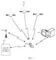
- FIG. 1is a block diagram of an exemplary mobile device communicating with a plurality of wireless systems, in accordance with an embodiment of the invention.
- FIG. 2is a block diagram of an exemplary time slot arrangement, in accordance with an embodiment of the invention.
- FIG. 3is a block diagram of an exemplary system for sharing components in a time division multiplex wireless system, in accordance with an embodiment of the invention.
- FIG. 4is a block diagram of an exemplary control and data interface, in accordance with an embodiment of the invention.
- FIG. 5Ais a block diagram of an exemplary linear amplifier, which may be utilized in connection with an embodiment of the invention.
- FIG. 5Bis a diagram of an exemplary input/output relationship of a linear amplifier, which may be utilized in connection with an embodiment of the invention.
- FIG. 6is a block diagram of an exemplary TX processing system, in accordance with an embodiment of the invention.
- FIG. 7is a block diagram illustrating an exemplary flow diagram of a system for sharing components in a time division multiplex wireless system, in accordance with an embodiment of the invention.
- FIG. 8is a block diagram of an exemplary flow diagram for adjusting several power supplies and a bias voltage, in accordance with an embodiment of the invention.
- FIG. 9is a block diagram of an exemplary flow diagram for calibrating a delay buffer, in accordance with an embodiment of the invention.
- Certain embodiments of the inventionmay be found in a method and system for minimizing power consumption in a communication system.
- Exemplary aspects of the inventionmay comprise configuring a supply voltage of an amplifier to enable communication of data using a first communication protocol during a first timeslot in a TDM frame, reconfiguring the supply voltage of the amplifier to enable communication of data using a different communication protocol, and adjusting the supply voltage of the amplifier in proportion to the envelope of a baseband signal conforming to one of the communication protocols.
- the first and second communication protocolsmay conform to various communication protocols, such as WCDMA, HSDPA, HSUDPA, GSM, GPRS, EDGE, WiMAX, OFDM, UWB, ZigBee, and Bluetooth.
- the baseband signalmay be delayed by a number of samples before being input into the amplifier.
- the number of samplesmay be calculated by minimizing the amount of intermodulation distortion at the output of the amplifier.
- the supply voltagemay be generated by a switching regulator.
- the methodmay also include configure a bias voltage of the amplifier to enable communication over the various protocols as well as adjusting the bias voltage of the amplifier in proportion to the envelope of the baseband signal, where the bias voltage may control the gain of the amplifier.
- the bias voltagemay also be generated by a switching regulator.
- FIG. 1is a block diagram of an exemplary mobile device communicating with a plurality of wireless systems, in accordance with an embodiment of the invention.
- an RFID transceiver 104may comprise suitable logic, circuitry, and/or code that may enable near field communication (NFC) with a mobile device.
- NFCnear field communication
- the RFID transceiver 104may be implemented as part of an electronic toll collection application in which the RFID transceiver 104 may be located at a toll plaza.
- a mobile device 102 that support NFCmay, for example, be used to authorize toll payments.
- the cellular telephone tower 100may comprise suitable logic, circuitry, and or code that may enable transmitting information to and receiving information from a mobile device 102 .
- the cellular telephone tower 100may transmit and receive information utilizing a TDMA communication protocol, such as GSM.
- informationmay be communicated to the mobile device 102 during timeslots. For example, one timeslot may be used to receive information from the mobile device 102 and the other may be used to transmit information to the mobile device 102 . Other timeslots may be used to communicate with other mobile devices.
- the satellite communication system 103may comprise suitable logic, circuitry, and/or code that may enable a mobile device to determine its location on earth.
- the satellite communication system 103may be comprised of a plurality of satellites all working in concert so that a mobile device 102 may triangulate its position.
- the satellite communication system 103may be a global positioning satellite (GPS) system.
- GPSglobal positioning satellite
- the computer 101may comprise suitable logic, circuitry, and or code that may enable communicating data utilizing a variety of communication protocols.
- the computer 101may communicate data utilizing a WLAN protocol, such as 802.11, or a Bluetooth protocol.
- the computer 101may utilize these protocols to communicate to a mobile device 102 .
- the computer 101may discover and make itself accessible to the mobile device 102 .
- the mobile device 102may then initiate a data transfer to the computer 101 .
- the mobile device 102may transfer information stored in a subscriber identity module (SIM), such as an address book, to the computer utilizing one of the protocols.
- SIMsubscriber identity module
- the mobile device 102may comprise suitable logic, circuitry, and/or code that may enable receiving and transmitting information utilizing a plurality of communication protocols.
- the mobile device 102may utilize a time division multiple access (TDMA) protocol, such as GSM, for handling voice and data calls.
- TDMAtime division multiple access
- GSMtime division multiple access
- the mobile device 102may utilize two timeslots within a GSM frame to communicate voice data to a cellular telephone tower 100 .
- the mobile device 102may communicate to other devices utilizing other communication protocols during unused timeslots.
- the mobile device 102may communicate to a computer 101 utilizing a Bluetooth protocol.
- the mobile device 102may also receive information, such as GPS satellite information during other timeslots as well.
- the mobile device 102may also be enabled to receive NFC signals from an RFID transceiver 104 .
- Utilizing unused timeslots to communicate informationmay enable resources within the mobile device 102 to be used more efficiently.
- a PLLmay be configured to enable GSM RX operation during a first timeslot.
- the PLLmay be reconfigured to support other communication protocols, such as Bluetooth. Therefore, only one PLL may be necessary to support the two protocols.
- FIG. 2is a block diagram of an exemplary time slot arrangement, in accordance with an embodiment of the invention.
- a multi-frame 205a single frame 200 , a WCDMA RX timeslot 201 , a WCDMA TX timeslot 203 , a Bluetooth TX timeslot 202 , a GPS RX timeslot 204 , and a NFC RX timeslot 206 .
- the multi-frame 205may conform to a WCDMA standard described above.
- the multi-frame 205may comprise 26 frames, where the length of each frame may be 4.16 milliseconds. Some of the frames within the multi-frame may be used to communicate data to a mobile device 102 ( FIG. 1 ).
- the single frame 200may be one of a plurality of frames in the multi-frame 205 .
- the single frame 200may be divided into, for example, eight (8) timeslots.
- a mobile device 102may communicate utilizing a plurality of communication protocols within the single frame 200 .
- the mobile device 102may receive information from a cellular telephone tower 100 ( FIG. 1 ) during the WCDMA RX timeslot 201 and may transmit information to a cellular telephone tower 100 during the WCDMA TX timeslot 203 .
- the mobile device 102may be configured to communicate using other communication protocols.
- the mobile device 102may be configured to communicate to a computer using, for example a Bluetooth transmission system during the Bluetooth TX slot 202 .
- the mobile terminalmay also be configured to receive signals from a plurality of satellites during the GPS RX time slot 204 .
- the mobile terminalmay also be configured to receive signals from a radio broadcast station during the NFC RX time slot 206 .
- FIG. 3is a block diagram of an exemplary system for sharing components in a time division multiplex wireless system, in accordance with an embodiment of the invention.
- a software definable radio (SDR) 305may comprise a RX processing system 300 , a TX processing system 301 , a PLL 302 , an oscillator 303 , and a control block 304 .
- the DSP 306may comprise receive buffers 307 and transmit buffers 308 .
- the RX processing system 300may comprise suitable logic, code, and/or circuitry that may enable receiving RF signals corresponding to a plurality of communication protocols.
- the RX processing system 300may be adapted to receive WCDMA transmissions, such as UMTS or IS-95.
- the RX processing system 300may be further adapted to receive other forms of transmissions, for example, Bluetooth, WLAN, GPS, NFC, WLAN, ZigBee, and DVB-H.
- the RX processing system 300may comprise a plurality of filters, which may be tailored so that the selected transmission may be properly received.
- the RX processing system 300may include a band pass filter that may in one instance be centered around a carrier frequency associated with, for example, a cellular telephone tower 100 ( FIG.
- the RX processing system 300may be capable of receiving RF signals corresponding to one communication protocol in one timeslot and another communication protocol in another timeslot within the same frame.
- the RX processing system 300may convert the received signals into an I and Q representation for subsequent processing by, for example, a DSP.
- the TX processing system 301may comprise suitable logic, code, and/or circuitry that may enable transmitting signals corresponding to a plurality of communication protocols.
- the TX processing system 301may be adapted to receive I and Q representations of data to be communicated using a particular communication protocol, such as UMTS or IS-95.
- the TX processing system 301may be further adapted to transmit other forms of transmissions, for example, Bluetooth, WLAN, GPS, NFC, WLAN, ZigBee, and DVB-H.
- the TX processing system 301may comprise a plurality of filters and an RF power amplifier that may be configured so that the data may be transmitted utilizing the proper communication protocol.
- the TX processing system 301may include a band pass filter that may in one instance be center around a carrier frequency associated with, for example, a cellular telephone tower 100 , and in another instance may be centered around a carrier frequency associated with a Bluetooth signal from a computer 101 .
- the TX processing system 301may be capable of transmitting RF signals corresponding to one communication protocol in one timeslot and another communication protocol in another timeslot within the same frame.
- the TX processing system 301may also comprise a plurality of amplifiers and mixers.
- the TX processing system 301may comprise a power amplifier (PA) for amplifying low level RF signals so that they may be transmitted via an antenna.
- PApower amplifier
- Mixersmay be utilized for modulating I/O signals from the DSP 306 .
- the TX processing system 301may comprise drivers that may be utilized to match the input impedance of the PA.
- the various amplifiers, mixers, and driversmay comprise linear amplifiers.
- the oscillator 303may comprise suitable logic, circuitry, and/or code that may enable generation of a local oscillator signal with a particular frequency.
- the local oscillator signal from the oscillator 303may be input the RX processing system 300 , the TX processing system 301 and the PLL 302 .
- the local oscillator signalmay be used as the reference for a quadrature phase demodulator that may reside within the RX processing system 300 .
- the demodulatormay shift the carrier frequency of a received RX signal down to a baseband carrier frequency so that the RX signal may be converted into an I and Q domain.
- the PLL 302may comprise suitable logic, circuitry and/or code that may enable generating an output frequency that may be a multiple of an input frequency.
- the PLL 302may be a fractional N synthesizer.
- the PLLmay effectively generate an output signal that may have a frequency that may be a non-integer multiple of the frequency of an input signal, such as the output of the oscillator 303 .
- the output of the PLLmay be 1 Mhz*M/N where M and N may be integers.
- the PLLmay be configured to output a plurality of frequencies that may enable communicating information utilizing a plurality of communication protocols.
- the control block 304may comprise suitable logic, circuitry, and/or code that may enable configuration of a plurality of components within a SDR.
- the control block 304may comprise a plurality of registers. The registers may in turn be used to control the functionality of the various components that make up the SDR 305 .
- the control block 304may be interfaced to a data bus connected to the DSP 304 so that the DSP 304 may read and write to registers within the control block 304 .
- the control block 304may also control which of a plurality of communication protocols may be used at any given time.
- the control block 304may comprise a timer for triggering events. The events may be used to reconfigure the various components of the SDR 305 at specific time.
- a first eventmay be used to configure the SDR 305 so that a first timeslot may be used as WCDMA TX timeslot 203 ( FIG. 2 ).
- a subsequent eventmay reconfigure the SDR 305 so that a second timeslot may be used, for example, as a Bluetooth TX timeslot 202 ( FIG. 2 ). Having the controller perform this function may reduce the processing power requirements of the DSP 304 .
- the DSP 304may comprise suitable logic, circuitry and/or code that may enable may enable sending and receiving I and Q data to and from the SDR 305 as well as suitable logic, circuitry and/or code that may enable configuring the SDR 305 .
- the DSP 304may convert data from various sources into I and Q information and visa versa.
- the DSP 304may maintain information to be transmitted in a buffer until the SDR 305 may be ready to send the information.
- the DSP 304may comprise a plurality of transmit and receive buffers 308 and 307 corresponding to a plurality of communication protocols, such as WCDMA and Bluetooth.
- the non-volatile memory 309may comprise suitable logic, circuitry, and/or code that may enable storing data.
- the DSP 304may store various configuration settings within the non-volatile 611 so that the SDR 305 may be re-initialized after a system reset.
- An event from the Control blockmay be communicated to the DSP 304 that may indicate to the DSP 304 which type of I and Q data to send or receive.
- the control blockmay communicate an event to the DSP 304 indicating that the next time slot in, for example, a WCDMA frame may be used to transmit Bluetooth data.
- the DSP 304may switch to a buffer 308 corresponding to Bluetooth data and begin communicating I and Q samples corresponding to Bluetooth data to the SDR 305 after the event occurs.
- the control blockmay then communicate to the DSP 304 that the next slot may, for example, be utilized to communicate WCDMA TX information.
- the DSPmay then switch over to a buffer 308 corresponding to WCDMA TX data and output I and Q samples corresponding to that data to the SDR 305 .
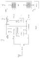
- FIG. 4is a block diagram of an exemplary control and data interface, in accordance with an embodiment of the invention.
- the timermay comprise suitable logic, circuitry, and/or code that may enable generation of periodic events.
- the periodicity of the timer and when events occurmay be configured by a processor, such as a DSP 306 .
- the lookup table 401may comprise suitable logic, circuitry, and/or code that may enable storing various hardware configuration settings corresponding to specific timeslots.
- the first element in the lookup table 401may comprise hardware configuration settings to be utilized during a first time slot in a TDMA frame.
- the subsequent elementsmay correspond to other timeslots within the same TDMA frame.
- a DSP 306may configure the timer, for example, to generate 8 timeslot event over a period of, for example, 4.16 milliseconds.
- a DSPmay program the lookup table 401 with configuration settings for a plurality of hardware components.
- the configuration settingsmay be settings that enable the hardware components within the SDR 305 ( FIG. 3 ) to process specific communication protocols.
- the second element in the lookup tablemay comprise configuration settings that may enable Bluetooth transmission.
- the fifth element in the lookup tablemay comprise configuration settings that may enable WCDMA transmission.
- the timermay output the configuration settings stored in the lookup time for every timeslot. For example, during a second timeslot the Bluetooth transmission configuration settings may be output.
- the control blockmay autonomously reconfigure the various hardware components, such as the RX processing system 300 ( FIG. 3 ), the TX processing system 301 ( FIG. 3 ), the PLL 302 ( FIG. 3 ), and the oscillator 303 ( FIG. 3 ).
- Reconfiguring the components for use with the various communication protocolsmay reduce the cost of the system because fewer components may be needed. This may result in a reduction in the board area required in a mobile device 102 ( FIG. 1 ). Additionally, power consumption may be reduced because the components may not be spending as much time in an idle mode.
- FIG. 5Ais a block diagram of an exemplary linear amplifier, which may be utilized in connection with an embodiment of the invention. Referring to FIG. 5A , there is shown a transistor 500 , a collector resistor (Rc) 504 , a bias resistor 503 , a bias input voltage 501 , a collector voltage 502 , an input signal 505 , and an output signal 506 .
- Rccollector resistor
- Rcbias resistor
- the collector of the transistor 500may be connected to a supply voltage 502 , via a collector resistor (Rc).
- a bias voltage 501may also be provided for controlling the voltage on the collector of the transistor 500 .
- the bias voltagemay then be modulated by an input signal 505 and 511 .
- the output signal 510may be an amplified version of the input signal.
- the bias voltage 501may be chosen so as to maximize the amount of voltage swing available for the output signal 510 .
- the bias voltage 501may be chosen so that the collector voltage on the transistor 500 is, for example, 50% of the supply voltage 502 . This may enable the greatest peak-to-peak voltage swing in the output signal 510 .
- the bias voltagemay also control the gain of the transistor.
- FIG. 5Bis a diagram of exemplary input/output characteristics of a linear amplifier, which may be utilized in connection with an embodiment of the invention. Referring to FIG. 5B , there is shown a transconductance curve 508 , an active region 509 , an input signal 511 , and an output signal 510 .
- the characteristics shown in FIG. 5Bmay correspond to the circuit shown in FIG. 5A Referring, to FIG. 5B , a lower bias voltage may result in a lower gain and conversely a higher bias voltage may result in a higher gain. In this regard, the gain of the transistor 500 may be non-linear when the variation of the output signal 510 may be large.
- the power dissipated in the circuit shown in FIG. 5Amay be dissipated by the collector resistor 504 and the transistor 500 .
- the power dissipated in the two componentsmay be represented by following formulas:
- the bias voltagemay be chosen so as to move the output signal 510 down on the curve shown in FIG. 5B . This may allow for a further reduction in the supply voltage and therefore may further lower the overall power dissipation in the circuit.
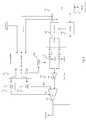
- FIG. 6is a block diagram of an exemplary TX processing system, in accordance with an embodiment of the invention.
- a power amplifier (PA) 604there is shown a power amplifier (PA) 604 , a pre-driver 600 , a delay buffer 606 , a calibrator 605 , a power controller 601 , a power supply 603 , a pre-driver power supply 608 , and a bias controller 607 .
- the pre-driver 600may comprise a driver 609 , and a pair of mixers 610 .
- the PA 604may comprise suitable logic, circuitry and or code that may enable amplifying an input signal so that it may be transmitted via an antenna.
- the internal structure of the PAmay comprise the circuitry shown in FIG. 5A . In this regard, in addition to an input and output signal, the PA may also have supply voltage input and a bias voltage input.
- the pre-driver 600may comprise suitable logic, code, and/or circuitry that may enable RE modulation of a baseband signal.
- the input signalmay be an in-phase and quadrature phase (I/O) representation of data to be transmitted.
- the I/Q datamay originate from a DSP 602 and pass through a delay buffer 606 before being input into the pre-driver 600 .
- the output of the pre-driver 600may be then output an RF signal to the PA 604 where it may then be amplified and transmitted via an antenna.
- the mixers 610may comprise suitable logic, circuitry, and/or code that may enable up-converting an input signal.
- the mixers 610may effectively output the product of the incoming signal and a local oscillator.
- the output of the mixermay be represented by the following formula:
- V ois the output of the mixer
- a 1 and A 2are the amplitudes of the respective inputs to the mixer 610
- ⁇ 1 and ⁇ 2are the period of the respective input signals.
- the mixer 610may effectively create replicas of the input signal at frequencies above and below the original signals frequency.
- a high-pass filtermay be used to strip off the lower frequency signal leaving only the up-converted or RF modulated signal.
- various buffersmay be utilized within the mixers 610 .
- the internal structure of these buffersmay comprise the circuitry shown in FIG. 5A .
- the buffersin addition to an input and output signal, the buffers may also have a supply voltage input and may be biased to have a predetermined gain.
- the output of the mixers 610may be added to together to create a composite output signal, which may then be input into a driver.
- the driver 609may comprise suitable logic, circuitry, and/or code that may enable amplifying or buffering and RF signal.
- the driver 609may be utilized to match the input impedance of the PA 604 .
- the driver 609may have a gain greater than one, in which case the output signal may be greater than the input signal.
- the internal structure of the driver 609may comprise the circuitry shown in FIG. 5A .
- the driver 609in addition to an input and output signal, the driver 609 may also have a supply voltage input and may be biased to have a predetermined gain.
- the delay buffer 606may comprise suitable logic, circuitry, and/or code that may enable delaying an input signal by a specified number of samples.
- the delay buffer 606may comprise a FIFO.
- the FIFOmay be sized to hold 10 I/Q samples.
- the samples leaving the delay buffermay be delayed by 10 samples.
- the I/Q samplesmay be communicated to the delay buffer by the DSP 602 and then passed on to the pre-driver 600 .
- the power controller 601may comprise suitable logic, circuitry, and/or code that may enable generation of a power supply and bias control reference voltage in proportion to the envelope of a signal.
- the power controller 601may input I/Q signals communicated from the DSP 602 .
- An envelope detectormay then analyze the incoming I/Q signals to determine an average amplitude of the signal.
- the power controller 601may collect a series of samples that may be used to determine an average signal amplitude or envelope of the signal.
- the power controller 601may comprise a memory for storing the samples.
- the power controller 601may then output a power supply reference voltage, bias controller reference voltage, and pre-driver power supply reference voltage. These reference voltages may be proportional to the average envelope computed. For example, if the envelope detector detects a signal with a large envelope, the reference voltages may be increased. Conversely, if a small envelope is detected the reference voltages may be decreased.
- the reference voltagesmay be output to the power supply 603 , bias controller 607 and pre-driver power supply 608 .
- the power controller 601may also adjust the various reference voltages in response to a control signal from the control block 304 ( FIG. 3 ).
- the control signal from the control block 304may enable the power controller 601 to converge to the correct voltage settings for the various reference voltages more quickly.
- the power controller 601may initially be configured to handle signals corresponding to, for example, WCDMA.
- the control block 304may then indicate that the next time slot is to be utilized for Bluetooth. If, for example, the envelope of a Bluetooth signal is always smaller than the envelope of a WCDMA signal, the power controller may quickly adjust the reference voltages down to voltages that correspond to the maximum envelope of a Bluetooth signal.
- the power supply 603 , bias controller 607 and pre-driver power supply 608may comprise suitable logic, circuitry, and/or code that may enable generation of an output voltage.
- the input voltage to the power supply 603 , bias controller 607 and pre-driver power supply 608may be larger or smaller than the respective outputs.
- the power supply 603 , bias controller 607 and pre-driver power supply 608may accomplish the conversion by utilizing a switch mode regulator.
- the regulatormay regulate the output voltage by converting the input voltage into a pulse and then varying the duty cycle of that pulse in response to a reference input. For example, given an input voltage of 10 volts, an output voltage of 5 volts may be obtained by generating a pulse with a 50% duty cycle. The pulse may then be filtered to obtain a DC voltage.
- the voltage output from the power supply 603 , bias controller 607 and pre-driver power supply 608may be controlled by the power controller 601 .
- the power supply 603 , bias controller 607 and pre-driver power supply 608may convert a higher voltage to a lower voltage while minimizing the power dissipation associated with such a conversion.
- the output of the power supply 603may be utilized to power the PA 604 .
- the output of the bias controller 607may be utilized to adjust the DC bias of the PA 604 and thus control the gain of the PA 604 .
- the output of the pre-driver power supply 608may be utilized to power the pre-driver 600 .
- the calibrator 605may comprise suitable logic, circuitry, and/or code that may enable minimizing the amount of intermodulation distortion (IMD) produced at the output of a PA.
- IMDintermodulation distortion
- the PA 604may not need as much headroom to handle signals with small envelopes.
- the supply voltage for the PA 604may be reduced.
- the PA 604may saturate. Therefore, the amount of delay in the pre-driver 600 and the power controller 601 must be matched so that the PA 604 may have enough headroom for a pending signal before the signal arrives at the PA 604 .
- the calibrator 605may match the delay of the power controller 601 and pre-driver 600 by measuring the amount of IMD at the output of the PA 604 . This may be accomplished by generating sinusoidal test signals in the DSP 602 , converting those signals into the I/Q domain and then passing the signals through the circuitry shown in FIG. 6 . For example, the DSP 602 may output a first test signal with a small envelope and then output a second signal with a larger envelope. When the delay, for example, is not matched, IMD may be produced at the output of the PA 604 . The calibrator 605 may use this information to adjust the amount of delay produced by the delay buffer 606 so as to reduce or eliminate IMD at the output of the PA 604 .
- the proper amount of delaymay be stored in a non-volatile memory 611 and re-read whenever the system may be re-enabled.
- an I/Q signalmay be communicated to both the delay buffer 606 and the power controller 601 .
- the power controller 601may store a series of I/Q samples so as to determine an average envelope. The power controller 601 may then determine that little or no gain in the PA 604 may be necessary. In this case, the bias voltage produced by the bias controller 607 may be reduced. This may allow for a reduced power supply voltage for the PA 604 as well. For example, referring to FIG. 5B , for lower gains, the active portion 509 may be moved to a lower point on the transconductance curve 508 by decreasing the bias voltage. As a result, the supply voltage for the PA 604 may be reduced as well.
- the active portionmay be moved to a higher point on the transconductance curve 508 by increasing the bias voltage.
- the power supply voltage for the PA 604may have to be increased. In this manner the power dissipation in the PA 604 may be minimized by supplying the minimum supply voltage necessary to avoid PA 604 saturation.
- the power controller 601may also lower the output of the pre-driver power supply 608 when the envelope of the signal is, for example, small. This may be possible because the headroom requirements of the driver 609 and the mixers 610 may be lower for lower signal envelopes. Reducing the power supply to the driver 609 and the mixers 610 may further reduce the overall power consumption of the system.
- the I/Q signals entering the pre-driver 600may have to be delayed by a predetermined number of samples via the delay buffer 606 . This may be necessary so that the power controller 601 may adjust the supply and bias voltages of the PA 604 before the modulated I/Q signals arrive at the input of the PA 604 . For example, if the delay is not set properly, the power supply voltage may be too low, in which case the PA may saturate. If the power supply voltage is too high, optimal power efficiency may not be achieved. Therefore, delaying the I/Q data entering the pre-driver 600 by the right number of samples may prevent the PA 604 from saturating and at the same time may minimize the amount of power dissipated by the PA 604 .
- the optimal delay for the delay buffer 606may be determined by the calibrator 605 .
- the calibrator 605may accomplish this by measuring the IMD produced by the test signals and adjusting the amount of delay produced by the delay buffer 606 so as to minimize the amount of IMD.
- FIG. 7is a block diagram illustrating an exemplary flow diagram of a system for sharing components in a time division multiplex wireless system, in accordance with an embodiment of the invention.
- the DSP 306may initialize the control block 304 ( FIG. 3 ) in the SDR 305 ( FIG. 3 ). This may involve configuring a timer 400 ( FIG. 4 ) for generating timeslot events.
- the DSP 306may, for example, configure the timer 400 so that the timer 400 generates a specific number of timeslot events over a given period of time.
- the DSP 306may configure the timer 400 so that it generates 8 timeslot events evenly distributed over, for example, 4.16 milliseconds.
- the DSP 306may also configure the control block 304 so that the control block 304 may control the various hardware components within the SDR 305 .
- the DSP 306may configure the control block 304 so that a first timeslot may be used for WCDMA RX 201 ( FIG. 2 ) and a second timeslot may be used for BT TX 202 ( FIG. 2 ).
- the control block 304may comprise a lookup table 401 ( FIG. 4 ) of configuration settings. Each entry in the lookup table 401 may contain various hardware configuration settings that may correspond to a particular timeslot within a TDMA frame, such as a WCDMA frame.
- the DSP 306may wait for the next timeslot.
- the control block 304may send a timeslot event for a particular timeslot if, for example, that timeslot may have been enabled for communication. If the communication over the current timeslot has been enabled, the control block 304 may generate a timeslot event to the DSP 306 at step 703 . Otherwise, step 701 may be repeated.
- the DSP 306may check if there may be any data to communicate. For example, in the case of data transmission, the DSP 306 may poll various buffers 308 ( FIG. 3 ) corresponding to various communication protocols to determine whether data needs to be communicated. In the case of data reception, the DSP 306 may check for I and Q data from the RX processing system 300 of the SDR 305 . If no communication is necessary, then step 701 may be repeated.
- the control block 304may configure various hardware components to enable communication for a particular protocol.
- the current timeslotmay have previously been configured for Bluetooth TX 202 .
- the control block 304may configure, for example, various filters within the RX processing system 300 ( FIG. 3 ) and the TX processing system 301 ( FIG. 3 ), the PLL 302 , the local oscillator 303 and the power controller 601 ( FIG. 6 ) within the TX processing system 301 the with values stored in a lookup table corresponding to the current timeslot.
- the DSP 306may communicate I and Q data to the TX processing system 301 of the SDR 305 in the case of data transmission, or the RX processing system 300 of the SDR 305 may communicate I and Q data to the DSP 306 in the case of data reception. After this, step 700 may be repeated.
- FIG. 8is a block diagram of an exemplary flow diagram for adjusting several power supplies and a bias voltage, in accordance with an embodiment of the invention.
- the power controller 601may buffer a series of I/Q samples from the DSP 602 . This may allow the envelope detector within the power controller 601 to determine the envelope of the signal at step 801 .
- the power controller 601may compute the gain and power supply requirements needed by the PA 604 as well as the power supply requirements for the driver 609 and mixers 610 in the pre-driver 600 . For example, for smaller envelopes, less gain and a lower supply voltage may be required. For larger envelopes, more gain and a higher supply voltage may be required.
- the power controller 601may take into consideration the type of signal being transmitted.
- the informationmay be communicated to the power controller 601 by the control block 304 ( FIG. 3 ).
- the power controller 601may initially be configured to handle signals corresponding to, for example, WCDMA.
- the control block 304may then indicate that the next time slot is to be utilized for Bluetooth.
- the power controllermay quickly adjust the reference voltages down to voltages that correspond to the maximum envelope of a Bluetooth signal. This may in turn lead to power savings in the system.
- the power controller 601may generate the appropriate reference voltages for the power supply 603 , bias controller 607 , and pre-driver power supply 608 .
- the power supply 603 , bias controller 607 , and pre-driver power supply 608may then provide the supply and bias voltages necessary for proper amplification of the signal.
- FIG. 9is a block diagram of an exemplary flow diagram for calibrating a delay buffer, in accordance with an embodiment of the invention.
- the amount of delay in the delay buffer 606may be set to a value well below an estimated optimal value.
- a sequence of sinusoidal test signalsmay be generated by the DSP.
- the DSPmay output a first test signal with a small envelope and then output a second signal with a larger envelope.
- IMDmay be produced at the output of the PA 604 .
- the IMDmay be measured by the calibrator at step 902 .
- the amount of IMDmay be compared to a threshold.
- the thresholdmay correspond to a level of IMD that may be acceptable. If the amount IMD is greater than the threshold, the amount of delay in the delay buffer 606 may be increased at step 904 . After this step, the IMD may be measured again and compared with the threshold. Once the amount of IMD is, for example, below the threshold, the process may stop and the optimal delay found may be stored to a non-volatile memory 611 for later retrieval.
- the power supply 602 for the PA 603may be configured to enable communication via a first communication protocol during a first timeslot of a TDM frame, reconfigured to enabled communication via a second communication protocol during a second timeslot of the TDM frame, and adjusted in proportion to the envelope of the baseband signal corresponding to the first and second communication protocols that is input into the PA 603 , where the communication protocols may correspond to an RF protocol, such as WCDMA, HSDPA, HSUDPA, GSM, GPRS, EDGE, WiMAX, OFDM, UWB, ZigBee, or Bluetooth, and may be delayed by a determined number of samples in the delay buffer 605 before being communicated to the PA 603 .
- an RF protocolsuch as WCDMA, HSDPA, HSUDPA, GSM, GPRS, EDGE, WiMAX, OFDM, UWB, ZigBee, or Bluetooth
- the bias voltage 606used to control the gain of the PA 602 may also be adjusted to enable communication via the communication protocols described above and adjusted in proportion to the envelope of the baseband signal as well.
- the number of samples and the corresponding amount of delay inserted by the delay buffer 605may be calculated by minimizing the amount of intermodulation distortion at the output of the PA 603 .
- the envelopemay be measured by evaluating a plurality of I and Q samples of the signal.
- the power supply 602 for the PA 603 and the bias controller 606may be switching regulators.
- the present inventionmay also be embedded in a computer program product, which comprises all the features enabling the implementation of the methods described herein, and which when loaded in a computer system is able to carry out these methods.
- Computer program in the present contextmeans any expression, in any language, code or notation, of a set of instructions intended to cause a system having an information processing capability to perform a particular function either directly or after either or both of the following: a) conversion to another language, code or notation; b) reproduction in a different material form.
Landscapes
- Engineering & Computer Science (AREA)
- Power Engineering (AREA)
- Physics & Mathematics (AREA)
- Nonlinear Science (AREA)
- Computer Networks & Wireless Communication (AREA)
- Signal Processing (AREA)
- Mobile Radio Communication Systems (AREA)
- Transmitters (AREA)
- Amplifiers (AREA)
- Transceivers (AREA)
Abstract
Description
- U.S. application Ser. No. 11/536,678, filed on Sep. 29, 2006;
- U.S. application Ser. No. 11/536,682, filed on Sep. 29, 2006;
- U.S. application Ser. No. 11/536,650, filed on Sep. 29, 2006;
- U.S. application Ser. No. 11/536,644, filed on Sep. 29, 2006;
- U.S. application Ser. No. 11/536,676, filed on Sep. 29, 2006;
- U.S. application Ser. No. 11/536,659, filed on Sep. 29, 2006;
- U.S. application Ser. No. 11/536,673, filed on Sep. 29, 2006;
- U.S. application Ser. No. 11/536,679, filed on Sep. 29, 2006;
- U.S. application Ser. No. 11/536,670, filed on Sep. 29, 2006;
- U.S. application Ser. No. 11/536,672, filed on Sep. 29, 2006;
- U.S. application Ser. No. 11/536,648, filed on Sep. 29, 2006;
- U.S. application Ser. No. 11/536,669, filed on Sep. 29, 2006;
- U.S. application Ser. No. 11/536,666, filed on Sep. 29, 2006;
- U.S. application Ser. No. 11/536,675, filed on Sep. 29, 2006;
- U.S. application Ser. No. 11/536,685, filed on Sep. 29, 2006;
- U.S. application Ser. No. 11/536,645, filed on Sep. 29, 2006;
- U.S. application Ser. No. 11/536,655, filed on Sep. 29, 2006;
- U.S. application Ser. No. 11/536,660, filed on Sep. 29, 2006;
- U.S. application Ser. No. 11/536,662, filed on Sep. 29, 2006;
- U.S. application Ser. No. 11/536,688, filed on Sep. 29, 2006;
- U.S. application Ser. No. 11/536,667, filed on Sep. 29, 2006;
- U.S. application Ser. No. 11/536,651, filed on Sep. 29, 2006;
- U.S. application Ser. No. 11/536,656, filed on Sep. 29, 2006;
- and U.S. application Ser. No. 11/536,663, filed on Sep. 29, 2006.
where Vc is the collector voltage set by the
where Vois the output of the mixer, A1and A2are the amplitudes of the respective inputs to the
S=√{square root over (I2+Q2)}
where S is the amplitude of the signal and I and Q are the respective in-phase and quadrature components of the signal. The
Claims (24)
Priority Applications (2)
| Application Number | Priority Date | Filing Date | Title |
|---|---|---|---|
| US13/252,402US8238285B2 (en) | 2006-09-29 | 2011-10-04 | Method and system for minimizing power consumption in a communication system |
| US13/558,248US8582497B2 (en) | 2006-09-29 | 2012-07-25 | Method and system for minimizing power consumption in a communication system |
Applications Claiming Priority (2)
| Application Number | Priority Date | Filing Date | Title |
|---|---|---|---|
| US11/536,657US8031651B2 (en) | 2006-09-29 | 2006-09-29 | Method and system for minimizing power consumption in a communication system |
| US13/252,402US8238285B2 (en) | 2006-09-29 | 2011-10-04 | Method and system for minimizing power consumption in a communication system |
Related Parent Applications (1)
| Application Number | Title | Priority Date | Filing Date |
|---|---|---|---|
| US11/536,657ContinuationUS8031651B2 (en) | 2006-09-29 | 2006-09-29 | Method and system for minimizing power consumption in a communication system |
Related Child Applications (1)
| Application Number | Title | Priority Date | Filing Date |
|---|---|---|---|
| US13/558,248ContinuationUS8582497B2 (en) | 2006-09-29 | 2012-07-25 | Method and system for minimizing power consumption in a communication system |
Publications (2)
| Publication Number | Publication Date |
|---|---|
| US20120093050A1 US20120093050A1 (en) | 2012-04-19 |
| US8238285B2true US8238285B2 (en) | 2012-08-07 |
Family
ID=39167481
Family Applications (3)
| Application Number | Title | Priority Date | Filing Date |
|---|---|---|---|
| US11/536,657Expired - Fee RelatedUS8031651B2 (en) | 2006-09-29 | 2006-09-29 | Method and system for minimizing power consumption in a communication system |
| US13/252,402Expired - Fee RelatedUS8238285B2 (en) | 2006-09-29 | 2011-10-04 | Method and system for minimizing power consumption in a communication system |
| US13/558,248ActiveUS8582497B2 (en) | 2006-09-29 | 2012-07-25 | Method and system for minimizing power consumption in a communication system |
Family Applications Before (1)
| Application Number | Title | Priority Date | Filing Date |
|---|---|---|---|
| US11/536,657Expired - Fee RelatedUS8031651B2 (en) | 2006-09-29 | 2006-09-29 | Method and system for minimizing power consumption in a communication system |
Family Applications After (1)
| Application Number | Title | Priority Date | Filing Date |
|---|---|---|---|
| US13/558,248ActiveUS8582497B2 (en) | 2006-09-29 | 2012-07-25 | Method and system for minimizing power consumption in a communication system |
Country Status (5)
| Country | Link |
|---|---|
| US (3) | US8031651B2 (en) |
| EP (1) | EP1916765A3 (en) |
| KR (1) | KR100926906B1 (en) |
| CN (1) | CN101175279B (en) |
| TW (1) | TWI389526B (en) |
Cited By (2)
| Publication number | Priority date | Publication date | Assignee | Title |
|---|---|---|---|---|
| US9277534B2 (en)* | 2008-02-06 | 2016-03-01 | Hmicro, Inc. | Wireless communications systems using multiple radios |
| US20210390362A1 (en)* | 2020-06-16 | 2021-12-16 | Denso Wave Incorporated | Interference suppression apparatus and interference suppression system |
Families Citing this family (17)
| Publication number | Priority date | Publication date | Assignee | Title |
|---|---|---|---|---|
| US8259834B2 (en) | 2006-09-29 | 2012-09-04 | Broadcom Corporation | Method and system for OFDM based MIMO system with enhanced diversity |
| US20080080455A1 (en) | 2006-09-29 | 2008-04-03 | Ahmadreza Rofougaran | Method and system for utilizing polarized antennas in coexistence systems |
| US8010067B2 (en)* | 2006-10-16 | 2011-08-30 | Goliath Solutions, Llc | Long range RFID transmitter power tracking loop |
| US7840685B2 (en) | 2007-01-07 | 2010-11-23 | Apple Inc. | Handheld computer having dynamic network transport selection according to a media type of a request |
| CN101114860B (en)* | 2007-08-17 | 2011-04-06 | 华为技术有限公司 | Method and device for controlling power amplification |
| US8064852B2 (en)* | 2008-11-13 | 2011-11-22 | Panasonic Corporation | Methods and apparatus for dynamically compensating for DC offset drift and other PVT-related signal variations in polar transmitters |
| EP2226932B1 (en)* | 2009-03-02 | 2013-10-16 | Alcatel Lucent | Method for amplifying a signal by a power amplifier, power amplifier system, device, computer program product, and digital storage medium thereof |
| US20130301497A1 (en)* | 2012-05-12 | 2013-11-14 | Broadcom Corporation | Wi-Fi proximity considerations within single user, multiple user, multiple access, and/or MIMO wireless communications |
| GB2505471A (en)* | 2012-08-31 | 2014-03-05 | Broadcom Corp | Time alignment of envelope and main signal paths in an envelope-tracking transmitter |
| DE102013201653A1 (en)* | 2013-01-31 | 2014-07-31 | Intel Mobile Communications GmbH | SWITCHING AND MOBILE COMMUNICATION DEVICE |
| TWI517614B (en)* | 2013-05-24 | 2016-01-11 | 凌通科技股份有限公司 | Bluetooth data/control message transmission module, interaction system and method thereof |
| RU2733905C2 (en)* | 2016-04-18 | 2020-10-08 | Рхомбус Сыстемс Гроуп, Инц. | System for communication with drones using two frequency bands |
| US11082013B2 (en)* | 2017-05-12 | 2021-08-03 | Mediatek Inc. | Method of reducing memory effect of power amplifier |
| CN107567008B (en)* | 2017-09-04 | 2020-11-13 | 太原理工大学 | EPC C C1G2 protocol improvement method based on CRFID label |
| US11032399B2 (en)* | 2018-12-14 | 2021-06-08 | EMC IP Holding Company LLC | Dynamic certification for configuration changes to software defined radio implemented devices |
| US11750324B2 (en)* | 2021-11-30 | 2023-09-05 | Analog Devices International Unlimited Company | Methods for adaptive error avoidance to increase re-transmission reliability in time-slotted communication links |
| FR3139692B1 (en)* | 2022-09-08 | 2024-09-13 | St Microelectronics Rousset | WIRELESS COMMUNICATION DEVICE CONFIGURED TO COMMUNICATE IN ULTRA WIDEBAND |
Citations (77)
| Publication number | Priority date | Publication date | Assignee | Title |
|---|---|---|---|---|
| US5423078A (en) | 1993-03-18 | 1995-06-06 | Ericsson Ge Mobile Communications Inc. | Dual mode power amplifier for analog and digital cellular telephones |
| US5426641A (en) | 1994-01-28 | 1995-06-20 | Bell Communications Research, Inc. | Adaptive class AB amplifier for TDMA wireless communications systems |
| US5475581A (en) | 1994-06-10 | 1995-12-12 | Westinghouse Electric Corp. | Waveform flat-topping unit |
| US5732334A (en) | 1996-07-04 | 1998-03-24 | Mitsubishi Denki Kabushiki Kaisha | Radio transmitter and method of controlling transmission by radio transmitter |
| US5878332A (en) | 1997-02-07 | 1999-03-02 | Eic Enterprises Corporation | Multiple frequency RF transceiver |
| US5963854A (en) | 1995-07-14 | 1999-10-05 | Lg Products Ab | Antenna amplifier |
| US6112062A (en) | 1997-09-26 | 2000-08-29 | The Whitaker Corporation | Predistortion for high power amplifiers |
| KR20010078104A (en) | 2000-01-28 | 2001-08-20 | 루센트 테크놀러지스 인크 | Power amplifier using upstream signal information |
| US20010031621A1 (en) | 1999-12-29 | 2001-10-18 | Schmutz Thomas R. | Automatic configuration of backhaul and groundlink frequencies in a wireless repeater |
| US20020015423A1 (en) | 1995-08-25 | 2002-02-07 | Rakib Selim Shlomo | Apparatus and method for trellis encoding data for transmission in digital data transmission systems |
| US20020045427A1 (en) | 2000-10-17 | 2002-04-18 | Saku Lahti | Method for receiving radio frequency signal and a receiver device |
| US6393299B1 (en) | 1997-07-15 | 2002-05-21 | Kabushiki Kaisha Toshiba | Radio communication equipment |
| US20020109635A1 (en) | 2001-02-09 | 2002-08-15 | Francis Geeraert | Antenna tuning |
| US20020132597A1 (en) | 2001-01-12 | 2002-09-19 | Peterzell Paul E. | Direct conversion digital domain control |
| US6456172B1 (en) | 1999-10-21 | 2002-09-24 | Matsushita Electric Industrial Co., Ltd. | Multilayered ceramic RF device |
| US20020140520A1 (en) | 2001-03-30 | 2002-10-03 | Hitachi Media Electronics Co., Ltd. | Radio frequency fliter, radio frequency circuit, antenna duplexer and radio terminal |
| KR20030006051A (en) | 2001-07-11 | 2003-01-23 | 현대자동차주식회사 | Intellectual recognition system and control process for driver |
| US20030021367A1 (en) | 2001-05-15 | 2003-01-30 | Smith Francis J. | Radio receiver |
| US20030109240A1 (en) | 2001-12-12 | 2003-06-12 | D.S.P.C. Technologies Ltd. | Method and polar-loop transmitter with origin offset for zero-crossing signals |
| US6594241B1 (en) | 1999-12-08 | 2003-07-15 | Telefonaktiebolaget Lm Ericsson (Publ) | Channel-type switching control |
| US20030169706A1 (en) | 2002-03-08 | 2003-09-11 | Frank Poegel | Switched combining antenna diversity technique |
| US20030193923A1 (en) | 1999-04-23 | 2003-10-16 | Abdelgany Mohyeldeen Fouad | Shared functional block multi-mode multi-band communication transceivers |
| US20030193997A1 (en) | 2001-01-26 | 2003-10-16 | Dent Paul W. | System and method for adaptive antenna impedance matching |
| US20030219035A1 (en) | 2002-05-24 | 2003-11-27 | Schmidt Dominik J. | Dynamically configured antenna for multiple frequencies and bandwidths |
| US20040014435A1 (en)* | 2002-07-12 | 2004-01-22 | Woo Sang-Hyun | Multi-band RF receiving method and apparatus in moblile communication system |
| US6708044B1 (en) | 2000-04-04 | 2004-03-16 | Nec America, Inc. | Apparatus and method for automated band selection via synthesizer bit insertion |
| US6714120B2 (en) | 1997-01-02 | 2004-03-30 | C. W. Over Solutions, Inc. | Inductor-capacitor resonant circuits and improved methods of using same |
| US6741847B1 (en) | 2000-06-28 | 2004-05-25 | Northrop Grumman Corporation | Multi-carrier receiver frequency conversion architecture |
| US20040131014A1 (en) | 2003-01-03 | 2004-07-08 | Microsoft Corporation | Frame protocol and scheduling system |
| US20040136473A1 (en) | 2002-12-05 | 2004-07-15 | Yang Chun Hua | Digital receiver |
| US20040196934A1 (en) | 2003-04-02 | 2004-10-07 | Dmitry Petrov | Programmable filter |
| US20040208157A1 (en) | 2001-10-22 | 2004-10-21 | Brian Sander | Multi-mode communications transmitter |
| US20040259594A1 (en) | 2003-04-22 | 2004-12-23 | Taek-Kyun Choi | Apparatus and method for simultaneously performing a TV reception function and a calling function in a mobile phone |
| US20040264403A1 (en) | 2003-06-25 | 2004-12-30 | Fette Bruce Alan | Definable radio and method of operating a wireless network of same |
| US6842440B2 (en) | 1985-03-20 | 2005-01-11 | Interdigital Technology Corporation | Subscriber RF telephone system for providing multiple speech and/or data signals simultaneously over either a single or a plurality of RF channels |
| US20050020299A1 (en) | 2003-06-23 | 2005-01-27 | Quorum Systems, Inc. | Time interleaved multiple standard single radio system apparatus and method |
| US20050032548A1 (en) | 2003-03-24 | 2005-02-10 | Frank Michael Louis | Method facilitating inter-mode handoff |
| US20050128978A1 (en) | 2002-04-16 | 2005-06-16 | Mark Pecen | Method and apparatus for compressed mode communication |
| US20050135502A1 (en) | 2003-12-17 | 2005-06-23 | Triquint Semiconductor, Inc. | Method and architecture for dual-mode linear and saturated power amplifier operation |
| US6917815B2 (en) | 2001-03-14 | 2005-07-12 | California Institute Of Technology | Concurrent dual-band receiver architecture |
| US20050181752A1 (en) | 2004-02-12 | 2005-08-18 | Sahota Gurkanwal S. | Wireless diversity receiver with shared receive path |
| US20050180353A1 (en) | 2004-02-13 | 2005-08-18 | Hansen Christopher J. | MIMO wireless communication greenfield preamble formats |
| US20050186933A1 (en) | 1997-07-31 | 2005-08-25 | Francois Trans | Channel equalization system and method |
| US20050245201A1 (en) | 2004-04-30 | 2005-11-03 | Nokia Corporation | Front-end topology for multiband multimode communication engines |
| US20050266811A1 (en) | 2004-06-01 | 2005-12-01 | Nokia Corporation | Ramp signal with boost portion preceding a time slot |
| US20050270216A1 (en) | 2003-06-19 | 2005-12-08 | Xuewen Jiang | Differential digital-to-analog converter |
| US20060056355A1 (en) | 2004-09-16 | 2006-03-16 | Love Robert T | System and method for downlink signaling for high speed uplink packet access |
| WO2006029082A2 (en) | 2004-09-03 | 2006-03-16 | Rf Micro Devices, Inc. | System and method for transitioning between modulation formats in adjacent bursts triggering on data flow |
| US20060068837A1 (en) | 2004-02-26 | 2006-03-30 | Quorum Systems, Inc. | Method and apparatus for synchronizing WLAN in a multi-mode radio system |
| US20060084469A1 (en) | 2004-03-10 | 2006-04-20 | Quorum Systems, Inc. | Transmitter and receiver architecture for multi-mode wireless device |
| US20060114836A1 (en) | 2004-08-20 | 2006-06-01 | Sofie Pollin | Method for operating a combined multimedia -telecom system |
| US20060154617A1 (en) | 2005-01-11 | 2006-07-13 | Clingman Dan J | Electrically tuned resonance circuit using piezo and magnetostrictive materials |
| US7088299B2 (en) | 2003-10-28 | 2006-08-08 | Dsp Group Inc. | Multi-band antenna structure |
| US20060202892A1 (en) | 2005-03-11 | 2006-09-14 | Nokia Corporation | Enhanced switched-beam antenna arrangement |
| US7110433B2 (en) | 1998-08-10 | 2006-09-19 | Kamilo Feher | Spread spectrum, cross-correlated and filtered modulated systems |
| US20060232419A1 (en) | 2005-04-13 | 2006-10-19 | Fujitsu Limited | RFID tag and antenna arranging method |
| US20060281423A1 (en) | 2004-10-15 | 2006-12-14 | Caimi Frank M | Methods and Apparatuses for Adaptively Controlling Antenna Parameters to Enhance Efficiency and Maintain Antenna Size Compactness |
| US20070001810A1 (en) | 2003-01-03 | 2007-01-04 | Scott Jeff W | Tags, wireless communication systems, tag communication methods, and wireless communications methods |
| US20070001813A1 (en) | 2005-07-01 | 2007-01-04 | Thingmagic, Inc. | Multi-reader coordination in RFID system |
| US20070025471A1 (en)* | 2005-06-24 | 2007-02-01 | Shaojie Chen | Communication apparatus including a buffer circuit having first and second portions for alternately storing results |
| US20070032246A1 (en) | 2005-08-03 | 2007-02-08 | Kamilo Feher | Air based emergency monitor, multimode communication, control and position finder system |
| US20070030116A1 (en) | 2005-08-03 | 2007-02-08 | Kamilo Feher | Multimode communication system |
| US20070032238A1 (en) | 2005-08-04 | 2007-02-08 | Samsung Electronics Co., Ltd | Method and system for performing handover between multiple modes using a single wireless receiver |
| US20070060071A1 (en) | 2005-09-15 | 2007-03-15 | Silicon Laboratories Inc. | Wireless communication system and method using digital calibration to control mixer input swing |
| US20070066245A1 (en) | 2005-09-22 | 2007-03-22 | Snider James R | Multiband or multimode front end antenna switch |
| US20070099580A1 (en) | 2004-03-04 | 2007-05-03 | Matsushita Electric Industrial Co., Ltd. | Frequency dividing circuit and multimode radio device using the same |
| US20070155344A1 (en) | 2005-12-29 | 2007-07-05 | Motorola, Inc. | Wireless multimode co-band receiver device and method employing receiver bypass control |
| US7245882B1 (en) | 2003-07-17 | 2007-07-17 | Atheros Communications, Inc. | Method and apparatus for a signal selective RF transceiver system |
| US20070173202A1 (en) | 2006-01-11 | 2007-07-26 | Serconet Ltd. | Apparatus and method for frequency shifting of a wireless signal and systems using frequency shifting |
| US20070184778A1 (en) | 2006-02-09 | 2007-08-09 | Eagle River Holdings Llc | System and method for communication utilizing time division duplexing |
| US20070238483A1 (en) | 2006-04-05 | 2007-10-11 | Olivier Boireau | Antenna sharing techniques |
| US20070259628A1 (en) | 2006-05-08 | 2007-11-08 | Harris Corporation | Multiband radio with transmitter output power optimization |
| US7295822B2 (en) | 2003-03-17 | 2007-11-13 | Casio Computer Co., Ltd. | Radio wave receiver, radio-controlled timepiece and tuning capacitance setting method |
| US20080007333A1 (en) | 2003-03-04 | 2008-01-10 | Lee Dong-Geun | Method and apparatus for controlling a power amplifier in a mobile communication system |
| US20090093270A1 (en) | 2006-03-31 | 2009-04-09 | Christian Block | Mobile Radio Module for Multiband-Multimode Operation |
| US20090097591A1 (en)* | 2007-10-10 | 2009-04-16 | Samsung Electronics Co., Ltd. | Apparatus and method for envelope tracking power amplification in wireless communication system |
| US7623835B2 (en) | 2000-10-03 | 2009-11-24 | Ian J Forster | Multi-band wireless communication device and method |
Family Cites Families (7)
| Publication number | Priority date | Publication date | Assignee | Title |
|---|---|---|---|---|
| US6175279B1 (en)* | 1997-12-09 | 2001-01-16 | Qualcomm Incorporated | Amplifier with adjustable bias current |
| US6272336B1 (en)* | 1998-12-30 | 2001-08-07 | Samsung Electronics Co., Ltd. | Traffic-weighted closed loop power detection system for use with an RF power amplifier and method of operation |
| US6349216B1 (en)* | 1999-07-22 | 2002-02-19 | Motorola, Inc. | Load envelope following amplifier system |
| US6313698B1 (en)* | 1999-09-24 | 2001-11-06 | Qualcomm Incorporated | Method and apparatus for wireless phone transmit power amplification with reduced power consumption |
| KR100837821B1 (en)* | 2003-02-14 | 2008-06-13 | 삼성전자주식회사 | Amplifier Control and Method for Power Saving |
| US7933570B2 (en)* | 2006-02-03 | 2011-04-26 | Quantance, Inc. | Power amplifier controller circuit |
| US7917106B2 (en)* | 2006-02-03 | 2011-03-29 | Quantance, Inc. | RF power amplifier controller circuit including calibrated phase control loop |
- 2006
- 2006-09-29USUS11/536,657patent/US8031651B2/ennot_activeExpired - Fee Related
- 2007
- 2007-04-13EPEP07007616Apatent/EP1916765A3/ennot_activeWithdrawn
- 2007-09-26CNCN2007101806265Apatent/CN101175279B/enactiveActive
- 2007-09-28TWTW096136211Apatent/TWI389526B/ennot_activeIP Right Cessation
- 2007-09-29KRKR1020070098503Apatent/KR100926906B1/ennot_activeExpired - Fee Related
- 2011
- 2011-10-04USUS13/252,402patent/US8238285B2/ennot_activeExpired - Fee Related
- 2012
- 2012-07-25USUS13/558,248patent/US8582497B2/enactiveActive
Patent Citations (79)
| Publication number | Priority date | Publication date | Assignee | Title |
|---|---|---|---|---|
| US6842440B2 (en) | 1985-03-20 | 2005-01-11 | Interdigital Technology Corporation | Subscriber RF telephone system for providing multiple speech and/or data signals simultaneously over either a single or a plurality of RF channels |
| US5423078A (en) | 1993-03-18 | 1995-06-06 | Ericsson Ge Mobile Communications Inc. | Dual mode power amplifier for analog and digital cellular telephones |
| US5426641A (en) | 1994-01-28 | 1995-06-20 | Bell Communications Research, Inc. | Adaptive class AB amplifier for TDMA wireless communications systems |
| US5475581A (en) | 1994-06-10 | 1995-12-12 | Westinghouse Electric Corp. | Waveform flat-topping unit |
| US5963854A (en) | 1995-07-14 | 1999-10-05 | Lg Products Ab | Antenna amplifier |
| US20020015423A1 (en) | 1995-08-25 | 2002-02-07 | Rakib Selim Shlomo | Apparatus and method for trellis encoding data for transmission in digital data transmission systems |
| US5732334A (en) | 1996-07-04 | 1998-03-24 | Mitsubishi Denki Kabushiki Kaisha | Radio transmitter and method of controlling transmission by radio transmitter |
| US6714120B2 (en) | 1997-01-02 | 2004-03-30 | C. W. Over Solutions, Inc. | Inductor-capacitor resonant circuits and improved methods of using same |
| US5878332A (en) | 1997-02-07 | 1999-03-02 | Eic Enterprises Corporation | Multiple frequency RF transceiver |
| US6393299B1 (en) | 1997-07-15 | 2002-05-21 | Kabushiki Kaisha Toshiba | Radio communication equipment |
| US20050186933A1 (en) | 1997-07-31 | 2005-08-25 | Francois Trans | Channel equalization system and method |
| US6112062A (en) | 1997-09-26 | 2000-08-29 | The Whitaker Corporation | Predistortion for high power amplifiers |
| US7110433B2 (en) | 1998-08-10 | 2006-09-19 | Kamilo Feher | Spread spectrum, cross-correlated and filtered modulated systems |
| US20030193923A1 (en) | 1999-04-23 | 2003-10-16 | Abdelgany Mohyeldeen Fouad | Shared functional block multi-mode multi-band communication transceivers |
| US6456172B1 (en) | 1999-10-21 | 2002-09-24 | Matsushita Electric Industrial Co., Ltd. | Multilayered ceramic RF device |
| US6594241B1 (en) | 1999-12-08 | 2003-07-15 | Telefonaktiebolaget Lm Ericsson (Publ) | Channel-type switching control |
| US20010031621A1 (en) | 1999-12-29 | 2001-10-18 | Schmutz Thomas R. | Automatic configuration of backhaul and groundlink frequencies in a wireless repeater |
| KR20010078104A (en) | 2000-01-28 | 2001-08-20 | 루센트 테크놀러지스 인크 | Power amplifier using upstream signal information |
| US6708044B1 (en) | 2000-04-04 | 2004-03-16 | Nec America, Inc. | Apparatus and method for automated band selection via synthesizer bit insertion |
| US6741847B1 (en) | 2000-06-28 | 2004-05-25 | Northrop Grumman Corporation | Multi-carrier receiver frequency conversion architecture |
| US7623835B2 (en) | 2000-10-03 | 2009-11-24 | Ian J Forster | Multi-band wireless communication device and method |
| US20020045427A1 (en) | 2000-10-17 | 2002-04-18 | Saku Lahti | Method for receiving radio frequency signal and a receiver device |
| US20020132597A1 (en) | 2001-01-12 | 2002-09-19 | Peterzell Paul E. | Direct conversion digital domain control |
| US20030193997A1 (en) | 2001-01-26 | 2003-10-16 | Dent Paul W. | System and method for adaptive antenna impedance matching |
| US20020109635A1 (en) | 2001-02-09 | 2002-08-15 | Francis Geeraert | Antenna tuning |
| US6917815B2 (en) | 2001-03-14 | 2005-07-12 | California Institute Of Technology | Concurrent dual-band receiver architecture |
| US20020140520A1 (en) | 2001-03-30 | 2002-10-03 | Hitachi Media Electronics Co., Ltd. | Radio frequency fliter, radio frequency circuit, antenna duplexer and radio terminal |
| US20030021367A1 (en) | 2001-05-15 | 2003-01-30 | Smith Francis J. | Radio receiver |
| KR20030006051A (en) | 2001-07-11 | 2003-01-23 | 현대자동차주식회사 | Intellectual recognition system and control process for driver |
| US20040208157A1 (en) | 2001-10-22 | 2004-10-21 | Brian Sander | Multi-mode communications transmitter |
| US20030109240A1 (en) | 2001-12-12 | 2003-06-12 | D.S.P.C. Technologies Ltd. | Method and polar-loop transmitter with origin offset for zero-crossing signals |
| US20030169706A1 (en) | 2002-03-08 | 2003-09-11 | Frank Poegel | Switched combining antenna diversity technique |
| US20050128978A1 (en) | 2002-04-16 | 2005-06-16 | Mark Pecen | Method and apparatus for compressed mode communication |
| US20030219035A1 (en) | 2002-05-24 | 2003-11-27 | Schmidt Dominik J. | Dynamically configured antenna for multiple frequencies and bandwidths |
| US7260424B2 (en) | 2002-05-24 | 2007-08-21 | Schmidt Dominik J | Dynamically configured antenna for multiple frequencies and bandwidths |
| US20040014435A1 (en)* | 2002-07-12 | 2004-01-22 | Woo Sang-Hyun | Multi-band RF receiving method and apparatus in moblile communication system |
| US20040136473A1 (en) | 2002-12-05 | 2004-07-15 | Yang Chun Hua | Digital receiver |
| US20070001810A1 (en) | 2003-01-03 | 2007-01-04 | Scott Jeff W | Tags, wireless communication systems, tag communication methods, and wireless communications methods |
| US20040131014A1 (en) | 2003-01-03 | 2004-07-08 | Microsoft Corporation | Frame protocol and scheduling system |
| US20080007333A1 (en) | 2003-03-04 | 2008-01-10 | Lee Dong-Geun | Method and apparatus for controlling a power amplifier in a mobile communication system |
| US7295822B2 (en) | 2003-03-17 | 2007-11-13 | Casio Computer Co., Ltd. | Radio wave receiver, radio-controlled timepiece and tuning capacitance setting method |
| US20050032548A1 (en) | 2003-03-24 | 2005-02-10 | Frank Michael Louis | Method facilitating inter-mode handoff |
| US20040196934A1 (en) | 2003-04-02 | 2004-10-07 | Dmitry Petrov | Programmable filter |
| US20040259594A1 (en) | 2003-04-22 | 2004-12-23 | Taek-Kyun Choi | Apparatus and method for simultaneously performing a TV reception function and a calling function in a mobile phone |
| US20050270216A1 (en) | 2003-06-19 | 2005-12-08 | Xuewen Jiang | Differential digital-to-analog converter |
| US20050020299A1 (en) | 2003-06-23 | 2005-01-27 | Quorum Systems, Inc. | Time interleaved multiple standard single radio system apparatus and method |
| US20040264403A1 (en) | 2003-06-25 | 2004-12-30 | Fette Bruce Alan | Definable radio and method of operating a wireless network of same |
| US7245882B1 (en) | 2003-07-17 | 2007-07-17 | Atheros Communications, Inc. | Method and apparatus for a signal selective RF transceiver system |
| US7088299B2 (en) | 2003-10-28 | 2006-08-08 | Dsp Group Inc. | Multi-band antenna structure |
| US20050135502A1 (en) | 2003-12-17 | 2005-06-23 | Triquint Semiconductor, Inc. | Method and architecture for dual-mode linear and saturated power amplifier operation |
| US20050181752A1 (en) | 2004-02-12 | 2005-08-18 | Sahota Gurkanwal S. | Wireless diversity receiver with shared receive path |
| US20050180353A1 (en) | 2004-02-13 | 2005-08-18 | Hansen Christopher J. | MIMO wireless communication greenfield preamble formats |
| US20060068837A1 (en) | 2004-02-26 | 2006-03-30 | Quorum Systems, Inc. | Method and apparatus for synchronizing WLAN in a multi-mode radio system |
| US20070099580A1 (en) | 2004-03-04 | 2007-05-03 | Matsushita Electric Industrial Co., Ltd. | Frequency dividing circuit and multimode radio device using the same |
| US20060084469A1 (en) | 2004-03-10 | 2006-04-20 | Quorum Systems, Inc. | Transmitter and receiver architecture for multi-mode wireless device |
| US20050245201A1 (en) | 2004-04-30 | 2005-11-03 | Nokia Corporation | Front-end topology for multiband multimode communication engines |
| US20050266811A1 (en) | 2004-06-01 | 2005-12-01 | Nokia Corporation | Ramp signal with boost portion preceding a time slot |
| US20060114836A1 (en) | 2004-08-20 | 2006-06-01 | Sofie Pollin | Method for operating a combined multimedia -telecom system |
| WO2006029082A2 (en) | 2004-09-03 | 2006-03-16 | Rf Micro Devices, Inc. | System and method for transitioning between modulation formats in adjacent bursts triggering on data flow |
| US20060056355A1 (en) | 2004-09-16 | 2006-03-16 | Love Robert T | System and method for downlink signaling for high speed uplink packet access |
| US20060281423A1 (en) | 2004-10-15 | 2006-12-14 | Caimi Frank M | Methods and Apparatuses for Adaptively Controlling Antenna Parameters to Enhance Efficiency and Maintain Antenna Size Compactness |
| US20060154617A1 (en) | 2005-01-11 | 2006-07-13 | Clingman Dan J | Electrically tuned resonance circuit using piezo and magnetostrictive materials |
| US20060202892A1 (en) | 2005-03-11 | 2006-09-14 | Nokia Corporation | Enhanced switched-beam antenna arrangement |
| US20060232419A1 (en) | 2005-04-13 | 2006-10-19 | Fujitsu Limited | RFID tag and antenna arranging method |
| US20070025471A1 (en)* | 2005-06-24 | 2007-02-01 | Shaojie Chen | Communication apparatus including a buffer circuit having first and second portions for alternately storing results |
| US20070001813A1 (en) | 2005-07-01 | 2007-01-04 | Thingmagic, Inc. | Multi-reader coordination in RFID system |
| US20070032246A1 (en) | 2005-08-03 | 2007-02-08 | Kamilo Feher | Air based emergency monitor, multimode communication, control and position finder system |
| US20070032266A1 (en) | 2005-08-03 | 2007-02-08 | Kamilo Feher | GPS and non GPS position finder, emergency, MIMO, spread spectrum, CDMA, GSM and OFDM |
| US20070030116A1 (en) | 2005-08-03 | 2007-02-08 | Kamilo Feher | Multimode communication system |
| US20070032238A1 (en) | 2005-08-04 | 2007-02-08 | Samsung Electronics Co., Ltd | Method and system for performing handover between multiple modes using a single wireless receiver |
| US20070060071A1 (en) | 2005-09-15 | 2007-03-15 | Silicon Laboratories Inc. | Wireless communication system and method using digital calibration to control mixer input swing |
| US20070066245A1 (en) | 2005-09-22 | 2007-03-22 | Snider James R | Multiband or multimode front end antenna switch |
| US20070155344A1 (en) | 2005-12-29 | 2007-07-05 | Motorola, Inc. | Wireless multimode co-band receiver device and method employing receiver bypass control |
| US20070173202A1 (en) | 2006-01-11 | 2007-07-26 | Serconet Ltd. | Apparatus and method for frequency shifting of a wireless signal and systems using frequency shifting |
| US20070184778A1 (en) | 2006-02-09 | 2007-08-09 | Eagle River Holdings Llc | System and method for communication utilizing time division duplexing |
| US20090093270A1 (en) | 2006-03-31 | 2009-04-09 | Christian Block | Mobile Radio Module for Multiband-Multimode Operation |
| US20070238483A1 (en) | 2006-04-05 | 2007-10-11 | Olivier Boireau | Antenna sharing techniques |
| US20070259628A1 (en) | 2006-05-08 | 2007-11-08 | Harris Corporation | Multiband radio with transmitter output power optimization |
| US20090097591A1 (en)* | 2007-10-10 | 2009-04-16 | Samsung Electronics Co., Ltd. | Apparatus and method for envelope tracking power amplification in wireless communication system |
Cited By (5)
| Publication number | Priority date | Publication date | Assignee | Title |
|---|---|---|---|---|
| US9277534B2 (en)* | 2008-02-06 | 2016-03-01 | Hmicro, Inc. | Wireless communications systems using multiple radios |
| US9595996B2 (en)* | 2008-02-06 | 2017-03-14 | Hmicro, Inc. | Wireless communications systems using multiple radios |
| US20170264338A1 (en)* | 2008-02-06 | 2017-09-14 | Hmicro, Inc. | Wireless communications systems using multiple radios |
| US20210390362A1 (en)* | 2020-06-16 | 2021-12-16 | Denso Wave Incorporated | Interference suppression apparatus and interference suppression system |
| US11755876B2 (en)* | 2020-06-16 | 2023-09-12 | Denso Wave Incorporated | Interference suppression apparatus and interference suppression system |
Also Published As
| Publication number | Publication date |
|---|---|
| HK1119010A1 (en) | 2009-02-20 |
| TWI389526B (en) | 2013-03-11 |
| KR100926906B1 (en) | 2009-11-17 |
| KR20080029939A (en) | 2008-04-03 |
| US20130021958A1 (en) | 2013-01-24 |
| TW200830822A (en) | 2008-07-16 |
| US20120093050A1 (en) | 2012-04-19 |
| EP1916765A3 (en) | 2009-06-17 |
| US20080080549A1 (en) | 2008-04-03 |
| CN101175279B (en) | 2011-04-13 |
| US8582497B2 (en) | 2013-11-12 |
| CN101175279A (en) | 2008-05-07 |
| US8031651B2 (en) | 2011-10-04 |
| EP1916765A2 (en) | 2008-04-30 |
Similar Documents
| Publication | Publication Date | Title |
|---|---|---|
| US8238285B2 (en) | Method and system for minimizing power consumption in a communication system | |
| US7729670B2 (en) | Method and system for minimizing power consumption in a communication system | |
| US8275068B2 (en) | Method and system for minimizing power consumption in a communication system | |
| US10361892B2 (en) | Selective power amplifier | |
| US8565121B2 (en) | Low latency frequency switching | |
| US7424276B2 (en) | Transmitter and wireless communication apparatus using the transmitter | |
| US10128798B2 (en) | Adjusting envelope tracking power supply | |
| EP3149860B1 (en) | Method and radio node for controlling radio transmission | |
| CN101682352A (en) | A radio frequency apparatus | |
| CN115277343A (en) | System and method for hybrid transmitter | |
| US8018913B2 (en) | Method and system for sharing components in a time division multiplex wireless system | |
| US20180034417A1 (en) | Power supply control | |
| US8909180B1 (en) | Method and apparatus for power supply modulation of a radio frequency signal | |
| US20240039480A1 (en) | Waveform-tailored average power tracking | |
| US20140155117A1 (en) | Shaping Table Reconfiguration At Communication Event Boundaries | |
| HK1119010B (en) | Method and system for minimizing power consumption in a communication system | |
| US20110293034A1 (en) | Method and system for minimizing power consumption in a communication system | |
| US9867135B1 (en) | Frequency-generating circuit and communications apparatus |
Legal Events
| Date | Code | Title | Description |
|---|---|---|---|
| ZAAA | Notice of allowance and fees due | Free format text:ORIGINAL CODE: NOA | |
| ZAAB | Notice of allowance mailed | Free format text:ORIGINAL CODE: MN/=. | |
| STCF | Information on status: patent grant | Free format text:PATENTED CASE | |
| AS | Assignment | Owner name:BANK OF AMERICA, N.A., AS COLLATERAL AGENT, NORTH CAROLINA Free format text:PATENT SECURITY AGREEMENT;ASSIGNOR:BROADCOM CORPORATION;REEL/FRAME:037806/0001 Effective date:20160201 Owner name:BANK OF AMERICA, N.A., AS COLLATERAL AGENT, NORTH Free format text:PATENT SECURITY AGREEMENT;ASSIGNOR:BROADCOM CORPORATION;REEL/FRAME:037806/0001 Effective date:20160201 | |
| REMI | Maintenance fee reminder mailed | ||
| FPAY | Fee payment | Year of fee payment:4 | |
| SULP | Surcharge for late payment | ||
| AS | Assignment | Owner name:AVAGO TECHNOLOGIES GENERAL IP (SINGAPORE) PTE. LTD., SINGAPORE Free format text:ASSIGNMENT OF ASSIGNORS INTEREST;ASSIGNOR:BROADCOM CORPORATION;REEL/FRAME:041706/0001 Effective date:20170120 Owner name:AVAGO TECHNOLOGIES GENERAL IP (SINGAPORE) PTE. LTD Free format text:ASSIGNMENT OF ASSIGNORS INTEREST;ASSIGNOR:BROADCOM CORPORATION;REEL/FRAME:041706/0001 Effective date:20170120 | |
| AS | Assignment | Owner name:BROADCOM CORPORATION, CALIFORNIA Free format text:TERMINATION AND RELEASE OF SECURITY INTEREST IN PATENTS;ASSIGNOR:BANK OF AMERICA, N.A., AS COLLATERAL AGENT;REEL/FRAME:041712/0001 Effective date:20170119 | |
| AS | Assignment | Owner name:AVAGO TECHNOLOGIES INTERNATIONAL SALES PTE. LIMITE Free format text:MERGER;ASSIGNOR:AVAGO TECHNOLOGIES GENERAL IP (SINGAPORE) PTE. LTD.;REEL/FRAME:047230/0133 Effective date:20180509 | |
| AS | Assignment | Owner name:AVAGO TECHNOLOGIES INTERNATIONAL SALES PTE. LIMITE Free format text:CORRECTIVE ASSIGNMENT TO CORRECT THE EFFECTIVE DATE OF MERGER TO 09/05/2018 PREVIOUSLY RECORDED AT REEL: 047230 FRAME: 0133. ASSIGNOR(S) HEREBY CONFIRMS THE MERGER;ASSIGNOR:AVAGO TECHNOLOGIES GENERAL IP (SINGAPORE) PTE. LTD.;REEL/FRAME:047630/0456 Effective date:20180905 | |
| MAFP | Maintenance fee payment | Free format text:PAYMENT OF MAINTENANCE FEE, 8TH YEAR, LARGE ENTITY (ORIGINAL EVENT CODE: M1552); ENTITY STATUS OF PATENT OWNER: LARGE ENTITY Year of fee payment:8 | |
| FEPP | Fee payment procedure | Free format text:MAINTENANCE FEE REMINDER MAILED (ORIGINAL EVENT CODE: REM.); ENTITY STATUS OF PATENT OWNER: LARGE ENTITY | |
| LAPS | Lapse for failure to pay maintenance fees | Free format text:PATENT EXPIRED FOR FAILURE TO PAY MAINTENANCE FEES (ORIGINAL EVENT CODE: EXP.); ENTITY STATUS OF PATENT OWNER: LARGE ENTITY | |
| STCH | Information on status: patent discontinuation | Free format text:PATENT EXPIRED DUE TO NONPAYMENT OF MAINTENANCE FEES UNDER 37 CFR 1.362 | |
| FP | Lapsed due to failure to pay maintenance fee | Effective date:20240807 |