US8237622B2 - Base sheet - Google Patents
Base sheetDownload PDFInfo
- Publication number
- US8237622B2 US8237622B2US12/521,244US52124407AUS8237622B2US 8237622 B2US8237622 B2US 8237622B2US 52124407 AUS52124407 AUS 52124407AUS 8237622 B2US8237622 B2US 8237622B2
- Authority
- US
- United States
- Prior art keywords
- chip
- antenna
- coil
- wireless
- base sheet
- Prior art date
- Legal status (The legal status is an assumption and is not a legal conclusion. Google has not performed a legal analysis and makes no representation as to the accuracy of the status listed.)
- Expired - Fee Related, expires
Links
Images


Classifications
- H—ELECTRICITY
- H01—ELECTRIC ELEMENTS
- H01Q—ANTENNAS, i.e. RADIO AERIALS
- H01Q21/00—Antenna arrays or systems
- H01Q21/29—Combinations of different interacting antenna units for giving a desired directional characteristic
- G—PHYSICS
- G06—COMPUTING OR CALCULATING; COUNTING
- G06K—GRAPHICAL DATA READING; PRESENTATION OF DATA; RECORD CARRIERS; HANDLING RECORD CARRIERS
- G06K19/00—Record carriers for use with machines and with at least a part designed to carry digital markings
- G06K19/06—Record carriers for use with machines and with at least a part designed to carry digital markings characterised by the kind of the digital marking, e.g. shape, nature, code
- G06K19/067—Record carriers with conductive marks, printed circuits or semiconductor circuit elements, e.g. credit or identity cards also with resonating or responding marks without active components
- G06K19/07—Record carriers with conductive marks, printed circuits or semiconductor circuit elements, e.g. credit or identity cards also with resonating or responding marks without active components with integrated circuit chips
- G06K19/077—Constructional details, e.g. mounting of circuits in the carrier
- G06K19/07749—Constructional details, e.g. mounting of circuits in the carrier the record carrier being capable of non-contact communication, e.g. constructional details of the antenna of a non-contact smart card
- G06K19/0775—Constructional details, e.g. mounting of circuits in the carrier the record carrier being capable of non-contact communication, e.g. constructional details of the antenna of a non-contact smart card arrangements for connecting the integrated circuit to the antenna
- G06K19/07756—Constructional details, e.g. mounting of circuits in the carrier the record carrier being capable of non-contact communication, e.g. constructional details of the antenna of a non-contact smart card arrangements for connecting the integrated circuit to the antenna the connection being non-galvanic, e.g. capacitive
- G—PHYSICS
- G06—COMPUTING OR CALCULATING; COUNTING
- G06K—GRAPHICAL DATA READING; PRESENTATION OF DATA; RECORD CARRIERS; HANDLING RECORD CARRIERS
- G06K19/00—Record carriers for use with machines and with at least a part designed to carry digital markings
- G06K19/06—Record carriers for use with machines and with at least a part designed to carry digital markings characterised by the kind of the digital marking, e.g. shape, nature, code
- G06K19/067—Record carriers with conductive marks, printed circuits or semiconductor circuit elements, e.g. credit or identity cards also with resonating or responding marks without active components
- G06K19/07—Record carriers with conductive marks, printed circuits or semiconductor circuit elements, e.g. credit or identity cards also with resonating or responding marks without active components with integrated circuit chips
- G06K19/077—Constructional details, e.g. mounting of circuits in the carrier
- G06K19/07749—Constructional details, e.g. mounting of circuits in the carrier the record carrier being capable of non-contact communication, e.g. constructional details of the antenna of a non-contact smart card
- G06K19/07773—Antenna details
- G06K19/07777—Antenna details the antenna being of the inductive type
- G06K19/07779—Antenna details the antenna being of the inductive type the inductive antenna being a coil
- G06K19/07783—Antenna details the antenna being of the inductive type the inductive antenna being a coil the coil being planar
- H—ELECTRICITY
- H01—ELECTRIC ELEMENTS
- H01Q—ANTENNAS, i.e. RADIO AERIALS
- H01Q1/00—Details of, or arrangements associated with, antennas
- H01Q1/12—Supports; Mounting means
- H01Q1/22—Supports; Mounting means by structural association with other equipment or articles
- H01Q1/2208—Supports; Mounting means by structural association with other equipment or articles associated with components used in interrogation type services, i.e. in systems for information exchange between an interrogator/reader and a tag/transponder, e.g. in Radio Frequency Identification [RFID] systems
- H—ELECTRICITY
- H01—ELECTRIC ELEMENTS
- H01Q—ANTENNAS, i.e. RADIO AERIALS
- H01Q1/00—Details of, or arrangements associated with, antennas
- H01Q1/36—Structural form of radiating elements, e.g. cone, spiral, umbrella; Particular materials used therewith
- H01Q1/38—Structural form of radiating elements, e.g. cone, spiral, umbrella; Particular materials used therewith formed by a conductive layer on an insulating support
- H—ELECTRICITY
- H01—ELECTRIC ELEMENTS
- H01Q—ANTENNAS, i.e. RADIO AERIALS
- H01Q7/00—Loop antennas with a substantially uniform current distribution around the loop and having a directional radiation pattern in a plane perpendicular to the plane of the loop
- H—ELECTRICITY
- H01—ELECTRIC ELEMENTS
- H01Q—ANTENNAS, i.e. RADIO AERIALS
- H01Q9/00—Electrically-short antennas having dimensions not more than twice the operating wavelength and consisting of conductive active radiating elements
- H01Q9/04—Resonant antennas
- H01Q9/16—Resonant antennas with feed intermediate between the extremities of the antenna, e.g. centre-fed dipole
- H—ELECTRICITY
- H04—ELECTRIC COMMUNICATION TECHNIQUE
- H04B—TRANSMISSION
- H04B5/00—Near-field transmission systems, e.g. inductive or capacitive transmission systems
- H04B5/20—Near-field transmission systems, e.g. inductive or capacitive transmission systems characterised by the transmission technique; characterised by the transmission medium
- H04B5/24—Inductive coupling
- H04B5/26—Inductive coupling using coils
- H04B5/266—One coil at each side, e.g. with primary and secondary coils
Definitions
- the present inventionrelates to a base sheet provided with a chip and an antenna.
- the inventionrelates to a technology for connecting, in a noncontact manner, to a chip including a circuit for storing information readable or identifiable on the basis of a signal wave transmitted from a reader/writer and to an antenna for receiving the signal wave transmitted from the reader/writer.
- a wireless IC tag or a wireless IC card(hereafter referred to as a “wireless IC tag/card”) is a product in the entrance to ubiquitous era.
- an RFIDradio frequency identification/radio frequency IC tag
- an RFIDradio frequency identification/radio frequency IC tag
- applicationssuch as the identification of a name plate or a product and the management of parts, materials, intermediate products, finished products, or the like in a plant, such as the assortment thereof.
- Wireless IC tags/cardsare also used in repeatedly usable, prepaid train cards (e.g., Suica cards issued by the East Japan Railway Company, etc.) and commutation cards, both of which operate only near readers/writers, electronic money, and the like.
- prepaid train cardse.g., Suica cards issued by the East Japan Railway Company, etc.
- commutation cardsboth of which operate only near readers/writers, electronic money, and the like.
- these wireless IC tags/cardsdo not include a power supply such as a battery and receives and rectifies a readout signal wave transmitted from a reader/writer, and convert the resultant power into a direct-current power source for driving a control circuit or a memory.
- a power supplysuch as a battery
- receives and rectifies a readout signal wave transmitted from a reader/writerand convert the resultant power into a direct-current power source for driving a control circuit or a memory.
- a high frequencysuch as a 900 MHz range or a 2.45 GHz range is used as a radio frequency to keep a readout distance of several tens centimeters to several meters.
- the wireless IC tag/cardincludes an antenna for transmitting a radio wave or receiving a transmitted radio wave, such as a dipole antenna.
- FIG. 1Ashows a plan view of a substrate sheet according to the present invention and is a disposition plan view of an exaggerated wireless IC (RFID) chip and a dipole antenna magnetically coupled according to the present invention.
- RFIDexaggerated wireless IC
- FIG. 1Bis an enlarged plan view of the wireless IC chip.
- FIG. 2is a schematic perspective external view showing a magnetic coupling system including a circular coil for antenna coupling and an on-chip coil used in an experiment and a simulation.
- FIG. 3is schematic plan view of an LC tank circuit used in an experiment of magnetic coupling according to the present invention.
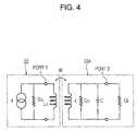
- FIG. 4is an electric circuit diagram showing a model used in a calculation of power transmission caused by magnetic coupling according to the present invention.
- FIG. 5is a Smith chart (experimental values) of a reflection coefficient of a system for coupling with an on-chip coil seen from a reader/writer coil.
- FIG. 6is a Smith chart (simulation values) of a reflection coefficient of a system for coupling with an on-chip coil seen from a reader/writer coil.
- FIG. 7is a graph showing the dependence of a power transmission loss from the reader/writer coil to the on-chip coil on the distance (gap) between the coils.
- FIG. 8is a plan view showing an actual disposition relation between the wireless IC chip and dipole antenna shown FIG. 1A in the form of an image.
- FIG. 9is a disposition plan view of a loop antenna to be magnetically coupled with a wireless IC chip in a case where the wireless IC chip is located inside the loop antenna.
- FIG. 10is a disposition plan view of a loop antenna to be magnetically coupled with a wireless IC chip in a case where the wireless IC chip is located outside the loop antenna.
- FIG. 11is a disposition plan view of a wireless IC chip and a spiral monopole antenna.
- FIG. 12is a perspective external view of a loop antenna of a reader/writer to be magnetically coupled with a loop antenna on a base sheet.
- FIG. 13includes a disposition plan view (A) of a monopole antenna, where which one surface of a wireless IC chip is connected to the inner end of a spiral of the monopole antenna, and a sectional view (B) taken along line X 2 -X 2 of (A).
- FIG. 14is a plan view showing an example disposition of a meander antenna having multiple magnetic coupling parts and possible multiple chips.
- FIG. 15is a disposition plan view of a loop antenna where a wireless IC chip overlaps the loop antenna.
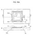
- FIG. 16Aincludes a plan view (A) of a coupling unit in a case where a wireless IC chip is vertically reversed and a sectional view (B) taken along line X 3 -X 3 of (A).
- FIG. 16Bincludes a plan view (A) of a coupling unit in a case where a wireless IC chip is disposed on a side of a base sheet other than a side thereof on which an antenna coupling part is disposed and a sectional view (B) taken along line X 4 -X 4 of (A).
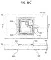
- FIG. 16Cincludes a plan view (A) of a coupling unit in a case where a wireless IC chip is interposed between or embedded in a base sheet and a sheet and a sectional view (B) taken along line X 5 -X 5 of (A).
- FIG. 16Dincludes a plan view (A) of a coupling unit in a case where an antenna coupling part is interposed between or embedded in a base sheet and a sheet and a sectional view (B) taken along line X 6 -X 6 of (A).
- FIG. 16Eincludes a plan view (A) of a coupling unit in a case where a wireless IC chip and an antenna coupling part are interposed between or embedded in a base sheet and a sheet and a sectional view (B) taken along line X 7 -X 7 of (A).
- FIG. 16Fincludes a plan view (A) of a coupling unit in a case where a wireless IC chip and an antenna coupling part are interposed between or embedded in a base sheet and two sheets and a sectional view (B) taken along line X 8 -X 8 of (A).
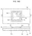
- FIG. 16Gincludes a plan view (A) of a coupling unit in a case where a wireless IC chip is interposed between or embedded in a base sheet and a sheet and a coating is applied to an antenna coupling part, and a sectional view (B) taken along line X 9 -X 9 of (A).
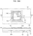
- FIG. 16Hincludes a plan view (A) of a coupling unit in a case where an antenna coupling part is interposed between or embedded in a base sheet and a sheet and a coating is applied to a chip, and a sectional view (B) taken along line X 10 -X 10 of (A).
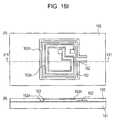
- FIG. 16Iincludes a plan view (A) of a coupling unit in a case where a coating is applied to a wireless IC chip and an antenna coupling part on a base sheet, and a sectional view (B) taken along line X 11 -X 11 of (A).
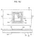
- FIG. 16Jincludes a plan view (A) of a coupling unit in a case where a wireless IC chip and an antenna coupling part are disposed on opposed sides of a base sheet and a coating is applied to the wireless IC chip and antenna coupling part, and a sectional view (B) taken along line X 12 -X 12 of (A).
- FIG. 17includes a plan view (A) of a sheet in which loop antennas to be magnetically coupled with one wireless IC chip are disposed in two layers, that is, upper and lower layers, and a sectional view (B) taken along line X 13 -X 13 of (A).
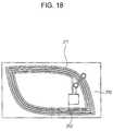
- FIG. 18is a front view showing a configuration of a related-art noncontact loop antenna-type IC card.
- FIG. 19is a schematic diagram showing a state in which a related-art reader/writer is reading out data in stored in a wireless IC tag.
- FIG. 20includes a disposition diagram (A) of parts of a related-art noncontact dipole antenna-type IC card and a sectional view (B) taken along line X 1 -X 1 of (A).
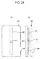
- FIG. 21includes drawings (a plan view (A) and a sectional view (B)) showing a structure (FIG. 6.9 in Non-Patent Document 2) of a ticket of the 2005 World Exposition.
- FIG. 22is a schematic diagram of “Love Earth Expo” admission system that is an example of an RFID system.
- FIG. 23is a perspective view showing an example of a train ticket card (related-art noncontact IC card) readout apparatus.
- FIG. 24is a schematic view showing that a reader/writer coil and an IC card coil are magnetically coupled so as to read out data from a magnetic coupling-type noncontact IC card.
- FIG. 25includes diagrams showing two examples (A) and (B) of functions included in an ultrasmall wireless IC chip.
- a reader/writeruses an antenna for transmitting or receiving a readout signal wave.
- an antennafor transmitting or receiving a readout signal wave.
- information stored in an RFIDcan be read out even from a distance of several tens of centimeters to several meters. For example, this allows assorting cargoes such as products.
- the above-mentioned prepaid ticket carduses a low frequency such as 13.56 MHz as a radio frequency so that a signal is exchanged only when bringing the card close to a ticket gate up to a distance of several centimeters therefrom.
- the prepaid ticket cardincludes a spiral coil much smaller (several centimeters or so) than the wavelength of a radio frequency and a wireless IC coupled to the spiral coil.
- FIG. 18An example structure of such a ticket card is shown in FIG. 18 .
- “ 210 ”represents a ticket card
- “ 211 ”represents a spiral coil
- “ 212 ”represents a wireless IC.
- the spiral coil 211allows a ticket card 210 and a reader/writer coil included in a ticket gate machine to be magnetically coupled when the ticket card 210 is brought close to the ticket gate machine so that information necessary for ticket examination is automatically exchanged.
- FIG. 19shows an outline configuration of a system for reading out data from a wireless IC tag.
- the left part of FIG. 19is a reader/writer 221 and the right part thereof is a wireless IC tag 222 .
- the reader/writer 221includes a control circuit/memory circuit 221 a , a modulation circuit 221 b , a detector/demodulation circuit 221 c , a circulator 221 d serving as a transmission/reception branching filter, an antenna 221 e , and the like.
- the wireless IC tag 222includes an antenna 222 a , a rectifier circuit 222 b , a demodulation circuit 222 c , a congestion control circuit/memory circuit 222 d , a modulation circuit 222 e , a load switch transistor 222 f , and the like.
- the reader/writer 221transmits instruction information for reading out the data in the form of a digital signal from the control circuit 221 a .
- the modulation circuit 221 breceives the digital signal and modulates a carrier wave having a radio frequency (typically, a frequency in the 900 MHz or 2.45 GHz range) caused therein and then transmits the modulated carrier wave from the antenna 221 e via the circulator 221 d (irreversible circuit) serving as a transmission/reception branding filter.
- a radio frequencytypically, a frequency in the 900 MHz or 2.45 GHz range
- This modulated carrier wave(a signal having a radio frequency) is not only a signal modulated using the readout instruction information but also becomes direct-current driving power after received by the wireless IC tag 222 . Therefore, considering also an attenuation (presumably 10 to 20 dB) caused by the propagation of the carrier wave over a radio distance from the antenna 221 e of the reader/writer 221 to the antenna 222 a of the wireless IC tag 222 , the carrier wave is transmitted using power (roughly several hundreds mW) necessary and sufficient to drive the wireless IC tag 222 .
- the wireless IC tag 222receives the signal having a radio frequency transmitted from the reader/writer 221 via the antenna 222 a and transmits most of the received power (several mW) to the rectifier circuit 222 b to convert the power into direct-current power. Then, the wireless IC tag 222 temporarily accumulates the direct-current power by charging an internal capacitor (not shown) of the wireless IC tag 222 . The remaining power is sent to the demodulation circuit 222 c that operates by the direct-current power accumulated as described above, and is demodulated into the original readout instruction signal. This demodulated readout instruction signal is sent to the control circuit/memory circuit 222 d and operates therein so that information stored in this memory circuit is read out.
- the load switch transistor 222 fis on/off driven on the basis of the read-out information.
- the magnitude of an impedance with respect to the carrier wave having a radio frequencyis changed in a prescribed repetition cycle so that the impedance at a radio frequency seen from the antenna is switched.
- a reflection wave pulse-amplitude-modulated in accordance with a change in the reflection coefficient with respect to the carrier waveis transmitted from the antenna of the wireless IC tag 222 to the antenna of the reader/writer 221 .
- the reader/writer 221receives the pulse-amplitude-modulated reflection wave transmitted from the wireless IC tag 222 , leads the reflection wave to the detector/demodulation circuit 221 c via the circulator 221 b having a function of separating a transmission wave and a reception wave, demodulates and identifies data read out from the wireless IC tag, and stores the data in the memory circuit 221 a.
- FIG. 20schematically shows an example structure of a wireless IC tag.
- (A)shows a plan view of the wireless IC tag and (B) shows an enlarged sectional view taken along line X 1 -X 1 of (A).
- a wireless IC tag 230according to a related-art example has a structure in which a semiconductor chip 232 is mounted on a dipole antenna 231 formed on a substrate using printing wiring technology. While a simplest dipole antenna is shown in the illustrated example, the dipole antenna takes various shapes in accordance with the frequency or the design of the orientation thereof.
- the dipole antenna 231has a length that is approximately half a wavelength corresponding to a radio frequency and is allowed to efficiently receive power transmitted from the reader/writer 221 as described above.
- the dipole antenna 231is one of antennas having the simplest structure and has a low gain and no sharp orientation, it is advantageous in that it can receive radio waves (signals having a radio frequency) from any directions.
- the antennais not limited to the dipole antenna 231 .
- a loop antennamay be used.
- An antenna disposed on a sheetis sometimes called an “inlet.”
- a wireless IC tag 241 serving as a ticketis different from the configuration and structure of the card-type wireless IC tag shown in FIG. 20 in that the wireless IC tag 241 has a structure in which a semiconductor chip 243 is connected to a conductor foil 242 serving as an external antenna and the semiconductor chip 243 and conductor foil 242 are interposed between two pieces of plate-like paper 244 .
- these wireless IC tagshave the same basic functions.
- this systemstarts to work when wireless IC tags, that is, RFIDs (tickets) each including a semiconductor chip are manufactured at a ticket manufacturing plant 251 .
- Chip IDs and ticketsare manufactured at the ticket manufacturing plant 251 .
- the chip IDsare stored in a ticket management DB 252 .
- Basic function 253compiles and manages data on issued tickets, data on the authentication of entry and exit, and the like in real time.
- An entry/exit authentication gate 254is provided with the reader/writer 221 described with reference to FIG. 19 .
- the reader/writer 221transmits signal waves for reading out information to RFIDs from a position a predetermined range away from the RFIDs so as to write information sent to the memory circuit into the RFIDs or read out information stored in the RFIDs to use the read-out information for entry/exit management. Also, the reader/writer 221 shown in FIG. 19 is provided at a tour reservation gate located in front of each pavilion so that a reservation for admission to a pavilion that a visitor wants to visit is automatically made.
- RFIDswireless IC tags
- FIG. 23shows the appearance of a ticket gate machine.
- This ticket card readout/write systemthat is, the basic part of the ticket gate machine includes a reader/writer 262 provided at an entry/exit gate 261 and including a coil for coupling and a ticket card 263 that each user individually has.
- a reader/writer 262provided at an entry/exit gate 261 and including a coil for coupling and a ticket card 263 that each user individually has.
- the entry/exit gate 261the user holds the ticket card 263 over the reader/writer 262 .
- a coil of the reader/writer 262 and a coil of the ticket card 263are coupled by a magnetic field/magnetic flux 264 so that the transmission and reception (communications) of information and the transmission of power is performed.
- a rough internal structure of the ticket card 263is the same as that of the ticket card 210 shown in FIG. 18 .
- the ticket card 263includes the above-mentioned spiral coil 211 formed on a card substrate and a semiconductor chip 212 electrically connected to the coil using a technology such as bonding and intended to write or read out information.
- a magnetic field/magnetic flux that couples the reader/writer 262 included in the ticket gate machine and the ticket card 263is shown as a reference numeral 264 in FIG. 23 .
- An equivalent circuit representing the coupling state caused by the magnetic field/magnetic flux 264is shown in FIG. 24 .
- an RF unit 272modulates a carrier wave (electromagnetic field) having a frequency of 13.56 MHz using a signal including a control signal generated by a control unit 271 of the reader/writer 262 and intended to read out information from the ticket card 263 .
- This modulated carrier wavepasses a high-frequency current through a coil 273 connected to the reader/writer 262 .
- a magnetic field/magnetic flux(“ 264 ” in FIG. 23 ) is generated.
- the magnetic field/magnetic flux 264 generated by the modulated carrier waveprovides power for driving an electronic circuit in the ticket card 263 as well as a signal transmitted from the reader/writer 262 .
- the magnetic field/magnetic flux 264 generated by the coil 273 of the reader/writer 262is interlinked to couple with a spiral coil (coil 211 in FIG. 18 ) provided around the ticket card 263 and thus a signal and power are transmitted between the coils wirelessly.
- the two coilsare closely coupled. In other words, the amount of leakage of the generated magnetic flux must be small.
- the distance between the two coilsmust be a given value (several tens of mm in the case of the ticket card system using 13.56 MHz) or less. This distance is nearly in proportion to the sizes of the two coils. Therefore, if the sizes of coils are reduced, the distance between the two coils must be reduced in proportion to the sizes of the coils so as to ensure the same level of coupling.
- the manufacturing cost of a wireless IC tag/cardhas been gradually reduced and a wireless IC tag/card has been actually used in train cards, electronic money, and the like.
- the manufacturing cost of a wireless IC tag/cardis still relatively high as an RFID; therefore, applications of a wireless IC tag/card are limited and a wireless IC tag/card has not been widely used.
- an RFIDbecomes an ultrasmall chip measuring several hundred ⁇ m or less per side and becomes cheaper, it is considered to apply such an RFID to the identification of a document having a property value, such as a bank note or a marketable security.
- a property valuesuch as a bank note or a marketable security.
- an ultrasmall RFIDis embedded in a bank note or a marketable security that can be bent more easily than a card, it is conceivable that a counterfeit bank note or the like can be easily discovered and such ease of the discovery can prevent a bank note or the like from being counterfeited.
- Such an attempthas been made in various fields, as seen in Non-Patent Document 1.
- the present inventionwas made in such a background and relates to a technology for connecting a chip including a circuit for storing information readable or identifiable using a signal wave from a reader/writer and an antenna for receiving the signal wave transmitted from the reader/writer in a noncontact manner, and a base sheet provided with such a chip and an antenna.
- An IC chip having an RFID function described in Non-Patent Document 1is an ultrasmall, square chip measuring 450 ⁇ m per side and having a thickness of several tens of ⁇ m.
- the size of the IC chipis reduced as described above so as to make a chip made of a semiconductor (silicon) crashworthy against bending stress or the like. Also, such a reduction in size of the chip significantly reduces the manufacturing cost per chip.
- this chipSince this chip is much smaller than a typical RFID chip, it includes only required minimum circuits among an RF circuit, a power supply circuit, a command control circuit, a congestion control circuit, a clock generation circuit, a memory write control circuit, and an EEPROM (electrically writable and erasable memory) included in a typical RFID chip, like circuit blocks of a function-oriented IC tag chip (A) or circuit blocks of an ultrasmall size-oriented IC tag chip (B) shown in FIG. 25 (see FIG. 3.21 on page 50 in Non-Patent Document 2). Specifically, the chip includes only an RF circuit, a power supply circuit, a clock generation circuit, and a read-only memory (ROM) of 128 bits.
- ROMread-only memory
- an RFID chipIn order to make an RFID chip ultrasmall as described above, it is preferable to provide, on the chip, an antenna for receiving a signal wave transmitted from a reader/writer, reading out internal data, and transmitting the data.
- an RFID chipcan be easily made in a bank note or a marketable security so that the RFID chip is used, for example, to prevent a bank note or the like from being counterfeited, as described above.
- What is needed first for that purposeis to increase the frequency of a radio signal for reading out a signal so as to downsize an antenna.
- IMS rangea frequency range for industry, medical care, and science
- the spatial half-wavelengthis about 60 mm in this frequency range; therefore, this frequency range can be easily used in terms of size.
- Non-Patent Document 1a method of providing a spiral coil on an RFID chip, also providing a coil on a reader/writer, and coupling these coils typically by a magnetic field/magnetic flux. This method is a method devised under a technical idea similar to that seen in a wireless IC card such as the above-mentioned ticket card.
- This methodis a method of making a spiral coil, which is conventionally formed on a card substrate in the related art, much smaller than the wavelength so that the spiral coil acts as an inductance even at 2.45 GHz, forming the spiral coil on an IC chip, under a technical idea similar to that of a wireless IC card, bringing the on-chip coil and a reader/writer coil having a size similar to that of the on-chip coil close to each other so as to magnetically coupling the two coils, receiving a interrogation signal transmitted from the reader using a radio wave in a microwave range, and operating the chip so as to read out information stored in a ROM.
- a 2.45 GHz wireless IC tagusing the above-mentioned method will be described in more detail.
- this methoduses electromagnetic wave transmission-type antennas as the antenna of a reader/writer and the antenna of a wireless IC tag and typically uses a so-called “half-wavelength dipole antenna” having a length (approximately 60 mm) that is approximately half the spatial wavelength (approximately 120 mm) at an operational frequency of 2.45 GHz.
- the wireless IC chip and the dipole antennamust be electrically connected to each other. If two antenna connector ends of the wireless IC chip are disposed in an identical plane, a method as shown in FIG. 20 is used.
- electrical connectionis realized by using a method of boding a terminal 234 connected to a connection bump 233 provided on a surface of the wireless IC chip 232 to a conductor surface 236 of the antenna using an anisotropic, conductive adhesive 235 .
- This methodallows keeping insulation between two bumps distant from each other while allowing establishing electric transmission between a bump, which is extremely close to the antenna conductor, and the antenna conductor using the contact between metal particles contained in the adhesive.
- Non-Patent Documents 1 and 2describe a method for connecting a wireless IC chip having a structure in which connection electrodes are provided on the upper and lower sides of the chip, to an antenna.
- a method of placing a wireless IC chip on the conductor part of a dipole antenna and placing a conductor on the chip with an isotropic, conductive adhesive therebetween so as to interpose the chip between the conductor part and the conductor to ensure the connectionis used as a relatively practical method particularly for an ultrasmall chip.
- This methodallows manufacturing a chip itself at low cost by using a semiconductor manufacturing process; however, the method requires mechanical work such as bending and crimping of a fine object so as to connect the chip to an antenna and requires considerably fine work. Also, this method has a problem that there occurs a nonnegligible reduction in reliability of the connection due to stress, such as bending of the connection part with the antenna.
- the RFID chip technologyis used to identify a bank note or a marketable security made of paper, which can be bent more easily than a card, the following two problems must be resolved: (1) a chip for identification must be made very small (ultrasmall) so as to ensure a resistance against bending stress; and (2) in order to couple a circuit for identification in such an ultrasmall chip and a reader/writer away from the chip by a practical distance, an electromagnetic wave transmission-type antenna such as a dipole antenna must be coupled to this chip while ensuring low cost and high reliability.
- an antenna having a size equal to the wavelength of a radio frequencycannot be manufactured on a surface of a semiconductor chip sufficiently small to be fixed onto paper. This makes it difficult to realize magnetic coupling with a distant reader/writer.
- an antennathat is allowed to provide sufficient power even on a minute chip must be disposed and the antenna and chip must be connected to each other so that power is transmitted therebetween.
- the structure of the connectionmust be a structure that is allowed to obtain sufficient connection at an operational frequency and has durability such that the connection is not destroyed, for example, due to bending of a paper-like base.
- An object of the present inventionis to solve the above-mentioned problems, that is, to provide a base sheet having a structure that couples a chip measuring 1 mm or less on paper and an antenna line by only disposing the chip and antenna line in such a manner that the chip and antenna line are close to each other, without physically bringing the chip into contact with the antenna line.
- Another object of the present inventionis to provide a base sheet having a structure that is allowed to couple multiple chips and an antenna line on a paper-like base, specifically, a structure that is allowed to connect even a group of ultrasmall wireless IC chips (hereafter referred to as “RF powders”) looking like particles to an antenna line at low cost and to use the RFID above or inside the paper-like base despite the low cost.
- RF powdersultrasmall wireless IC chips
- a base sheet according to the present inventionis configured as described below.
- the base sheet according to the present inventionincludes: a chip wherein a spiral or helical coil having at least one turn is disposed on a surface of the chip, or inside the chip and near the surface; and an antenna line including a conductor orbiting around the coil of the chip or directly above or directly below the coil so that the conductor is magnetically coupled with the coil.
- the chippreferably includes a semiconductor circuit for storing wirelessly readable information as well as the coil disposed around the chip, and the coil and the semiconductor circuit are preferably electrically connected to each other.
- the conductor part of the antenna line to be magnetically coupled with the coil of the antenna line, the conductor part orbiting around the coil or directly above or directly below the coilis preferably spiral, helical, or loop-shaped and preferably has one turn or a plurality of turns.
- the conductor part of the antenna line to be magnetically coupled with the coilis preferably meandering, and a plurality of the chip are preferably disposed so that the chips are magnetically coupled with the antenna line.
- the antenna lineis preferably a dipole antenna.
- the antenna lineis preferably a loop antenna.
- a plurality of the antenna lineare formed in layers of a multilayered structure.
- a minute probe antennamust be brought close to a minute coil of a chip so as to obtain magnetic coupling with the chip. While this is suitable for an application where reading out is performed in proximity, this is not a method for transmitting high power in a short period. Accordingly, the related art method cannot operate an RFID including a memory or the like.
- power for operating a memory or logicis provided to a minute device even from a relatively distant position. Since a minute semiconductor chip is low-cost, a low-cost, particular RFID can be used in a bank note or a sheet-like base (base sheet), which must be confidential.
- the principle of electromagnetic transmissionis used as a method for transmitting power without requiring physical contact.
- This principleis typically used when transmitting high power at a low frequency using a power transformer.
- a microwavefor example, see Japanese Unexamined Patent Application Publication No. 2005-340658 (Japan Patent Application No. 2004-159960) “TRANSFORMER CIRCUIT AND MANUFACTURING METHOD THEREOF”).
- first and second coilsare disposed so that the lines of the coils overlap each other in upper and lower layers in such a manner that the lines are insulated from each other, on a thick insulating layer on a semiconductor chip and when a high-frequency is passed through the first coil, a current having an identical frequency is passed through the second coil by magnetic coupling if a circuit is closed. If the circuit is open, a voltage occurs at both edges. This is an action caused in accordance with Maxwell's equations of electromagnetism. Unlike a contact method, this coupling has an advantage that even if the distance between the two coils is changed slightly (by approximately one-tenth the length of the coils), such a change makes no significant change to the coupling for transmitting power. Magnetic coupling is significantly different from the contact method in which power cannot be transmitted if the contact is lost. Also, magnetic coupling makes a large allowance for the distance between the circuits.
- the present inventionmagnetically couples an antenna and a chip by forming a first coil for causing magnetic coupling on the chip and using a part of the antenna as the second coil described in the above-mentioned Patent Document (Japanese Unexamined Patent Application Publication No. 2005-340658). While physical connection requires a high-cost implementation process of connecting a minute chip to an antenna accurately, magnetic coupling is not required to be accurate in position setting like in physical connection. Also, since the two coils are physically distant from each other, there does not occur a problem that electrical contact is disrupted on bent paper thereby causing a failure.
- FIGS. 1A , 1 B, and 2Plan views of this base sheet are shown in FIGS. 1A , 1 B, and 2 .
- FIG. 1Ashows a plan view of the base sheet including a wireless IC chip and an antenna and
- FIG. 1Bshows an enlarged view of only the wireless IC chip.
- the wireless IC (RFID) chipis drawn on a relatively large scale in order to exaggerate the chip.
- RFIDwireless IC
- the base sheet 12is made of a flexible sheet material such as paper.
- the wireless IC chip 11is a chip formed by disposing a spiral coil 13 A on an oxide film formed on a silicon substrate.
- the coil 13 Ais connected to a circuit element or a functional circuit block formed inside or on the wireless IC chip 11 .
- An image of this connection stateis shown in FIG. 1B , which is an enlarged view.
- the functional circuit blockis a circuit including a wireless circuit, a control circuit, a memory circuit, a power supply circuit, and the like and serving as an RFID, for example, in FIGS. 25(A) and (B).
- the circuit elementare an MIM capacitor for matching circuits and a resistance.
- a first embodiment of the present inventionresolves the above-mentioned problem by using the two coils 13 A and 14 A disposed in such a manner that the coils are extremely close to each other, as the coupling parts between the wireless IC chip 11 and an antenna (or antenna line) 14 on the base sheet 12 .
- the inventorsmade the following two important technical examinations.
- One of the examinationsis the relation between the degree of the coupling between the two coils 13 A and 14 A and the distance therebetween.
- the relation between the distance and the degree of couplingwas obtained from an experiment and a simulation using spiral coils (one turn or two or more turns) formed in the form of a square measuring 450 ⁇ m per side.
- the inventorsunderstood that in order to obtain the practical degree of coupling using coils measuring 450 ⁇ m per side, the coils must be formed in almost identical sizes and vertically overlapped by each other and the vertical distance therebetween must be approximately 200 ⁇ m or less. Also, the inventors found that this distance is similar to the thickness (approximately 100 ⁇ m) of normal paper.
- FIG. 2shows a configuration used in the above-mentioned experiment.
- the configurationhas a structure that magnetically couples a two-turn circular helical coil 22 (on-substrate coil 22 ) formed on a polyimide substrate 21 with a thickness of 25 ⁇ m using a copper thin film and a three-turn spiral coil 33 A (on-chip coil 33 A) formed on a silicon chip 31 measuring 450 ⁇ m per side as shown in FIG. 3 .
- An MIM capacitor 32is connected to the spiral coil 33 A on the silicon chip 31 in parallel and is set so that the MIM capacitor resonates at approximately 2.45 GHz.
- FIG. 4shows an equivalent circuit including a signal source.
- This equivalent circuitis obtained using the input end of the above-mentioned helical coil 22 as a port 1 and both ends of the spiral coil 33 A on the silicon chip 31 as a port 2 serving as the output port.
- Irepresents a current source serving as a signal source
- G Grepresents a signal source conductance
- L Grepresents a self-inductance of the on-substrate coil 22
- Lrepresents a self-inductance of the on-chip coil 33 A
- Mrepresents a mutual inductance representing the coupling between the on-substrate coil 22 and on-chip coil 33 A
- Crepresents the capacity of the MIM capacitor
- G Orepresents a conductance representing a loss of a tank circuit including the on-chip coil 33 A and MIM capacitor 32
- GLrepresents a load connected to this tank circuit (in an actual wireless IC chip, this load corresponds to an RF circuit or the like).
- An example of the resultis shown in FIG. 5 as a reflection coefficient chart 51 (so-called “Smith chart”). In this chart, resonance is seen at approximately 2.5 GHz.
- the circuit disposition configuration shown in FIG. 2was analyzed using commercially available software for electromagnetic field simulation.
- a reflection coefficient seen from the port 1 of the on-substrate coil 22 under a condition (in a state in which the load in the equivalent circuit shown in FIG. 4 is not connected, that is, in a state of G L0) identical to the condition under which the experiment was conducted and a scattering coefficient matrix (also called “S parameter” or “S matrix”) using the ports 1 and 2 as the input end and output end were obtained with the distance between the two coils changed.
- S parameteralso called “S parameter” or “S matrix”
- a Smith chart 61 that is a reflection coefficient chart obtained in the simulationis shown in FIG. 6 . Since the values shown in this chart roughly match the experimental values shown in FIG. 5 , it is obviously no problem to use the results of simulations performed under other conditions as theoretical experiment results.
- FIG. 1Athe three-turn spiral coil 13 A on the wireless IC chip 11 and the one-turn coil 14 A disposed in the form of a loop in such a manner that the coil 14 A surrounds the coil 13 A as if the coil 14 A were going around the coil 13 A are magnetically coupled.
- FIG. 8is schematic diagram shown in such a manner that the size relation between the wireless IC chip 11 and antenna 14 is brought close to the actual size relation.
- the length of the antenna 14 on the base sheet 12that is, the length of the dipole antenna line is preferably half the wavelength; however, the size may be changed depending on the use purpose or due to a manufacturing limit.
- the coil 13 A on the wireless IC chip 11may be any of a single-turn coil, a spiral coil, and a helical coil. Also, the coil 13 A may take any shape such as a square, a polygon, a circle, or an ellipse.
- FIGS. 9 and 10a second embodiment of the present invention is shown in FIGS. 9 and 10 .
- An antenna 92forms a closed loop on a base sheet 91 .
- FIG. 9shows an example in which a wireless IC chip 93 is included in a loop-shaped coil 92 A formed by the antenna 92 and
- FIG. 10shows an example in which the wireless IC chip 93 is disposed outside the loop-shaped coil 92 A formed by the antenna 92 .
- a coil 93 A of the wireless IC chip 93 and the coil 92 A of the antenna 92are magnetically coupled.
- the coil 93 Ais connected to a circuit element or a functional block, like in the wireless IC chip 11 shown in FIG. 1A .
- the wireless IC chip 93is shown in an enlarged manner compared with the length of the line of the antenna 92 .
- the actual length of the loop shape of the antenna 92typically corresponds to the wavelength.
- the length of the antenna 92is designed in accordance with the wavelength and is on the order of several tens of mm.
- the two circuitsare magnetically coupled.
- Such couplingcauses a cross talk when designing the wiring of a integrated circuit and such a structure is a structure whose use should be avoided; however, the coil 93 A and the conductor are positively brought close to each other in order to increase transmission electromagnetic energy and the lengths of the parallel parts are increased.
- One of contact methodsis a method of overlapping the spiral coil of the wireless IC chip and the antenna (antenna line) to be magnetically coupled with the spiral coil with each other rather than a method of including the wireless IC chip.
- the on-chip coilis insulated, for example, using a plasma silicon nitride film serving as a protection film; therefore, the on-chip coil and the coil of the coupling part of the antenna line are insulated from each other by the insulating film.
- FIG. 11a method of winding the antenna line serving as the coupling part coil in a spiral manner.
- This methodis shown in FIG. 11 .
- “ 111 ”represent a base sheet
- “ 112 ”represents an antenna
- “ 112 A”represents a spirally wound
- “ 113 ”represents a wireless IC chip
- “ 113 A”represents an on-chip coil.
- the length of the coil 113 A on the wireless IC chip 113 on the base sheet 111is designed as appropriate depending on the frequency to be used and is wound spirally. In this case, the end of an internal line of the spiral coil 112 A must be taken out of the spiral.
- Such configurationcannot be provided by simply using a single-layer antenna line is used. For this reason, the antenna 112 is formed in two layers.
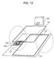
- FIG. 12shows a state in which an electromagnetic wave is transmitted from a loop antenna 124 for a reader/writer at a frequency of 2.45 GHz and the antenna 122 on a base sheet 121 receives this electromagnetic wave.
- a current having an identical frequencyis induced in the antenna 122 and a coil 123 A of a wireless IC chip 123 magnetically coupled with the antenna 122 receives this current.
- a power supply circuit of the wireless IC chip 123 for converting powergenerates and accumulates direct-current power necessary for an operation. Using this direct-current power, the wireless IC chip 123 transmits stored data from the on-chip coil 123 A to the antenna 122 via the magnetic coupling.
- a reader/writer 125which is put in readout mode, receives the data via the electromagnetic coupling between the antennas.
- the two antennasthat is, the antenna 122 of the reader/writer 125 and the antenna 124 of the base sheet 121 have an identical structure and an identical size
- a transmission characteristicwas obtained at a frequency near 2.4 GHz with the distance between the antennas changed using a simulation.
- the transmission losswas approximately the same and there was obtained a prospect that readout is possible even from a distance of 300 mm or so like in the case of the above-mentioned dipole antenna.
- the third embodimentis an example in which the coupling unit between a wireless IC chip and an antenna line is disposed at an end of the antenna line, the coupling part of the antenna line on a base sheet is a loop-shaped or spiral coil, and the wireless IC chip is disposed on a connection pad at the end of the antenna line.
- (A)is a plan view and (B) is a sectional view taken along line X 2 -X 2 of (A).
- the thickness of the base sheetis shown in an exaggerated manner. This applies to the following description of the embodiment.
- 131represents a base sheet
- 132represents an antenna line
- 132 Arepresents a spiral part (loop part) acting as the coupling part of the antenna line 132
- 132 Brepresents a connection pad
- 133represents a wireless IC chip
- 133 Arepresents a coil on the wireless IC chip 133 .
- One surface of the wireless IC chip 133is made of aluminum connected to a silicon substrate and fixed onto the connection pad 132 B formed at the inner end of the spiral part 132 A using a conductive adhesive (e.g., silver paste).
- the antenna lineis a one-fourth wavelength monopole antenna and is typically grounded via a coil connected to an end thereof.
- the coil of the antenna and the coil of the chipare used in a state in which these coils are connected to each other. Therefore, this method must connect one end of the antenna to the coil of the chip electrically. In this respect, this method has a problem similar to that of the related art.
- FIG. 14is a disposition plan view.
- a loop-shaped antenna 142 formed on a base sheet 141includes a meandering part (meander) 144 .
- the meandering part 144forms multiple coupling parts with multiple wireless IC chips 143 having different shapes.
- example wireless IC chips that do not fit into the coupling partare also shown.
- the antenna 142 having the bent meandering part 144 as described aboveis called a “meander antenna.”
- example wireless IC chips straddling the meander antenna 142are also shown. If the antenna line is disposed in such a manner that the antenna line cuts across the center of a wireless IC chip, a magnetic field having a reverse direction cuts across the wireless IC chip. As a result, magnetic coupling is not substantially obtained. Such a state occurs if many wireless IC chips are used in a powder manner in which the wireless IC chips are not controlled individually. However, there is a high probability that the wireless IC chips are always disposed in positions in which the wireless IC chips are magnetically coupled with the antenna line. Therefore, the wireless IC chips are used ignoring a case where magnetic coupling does not occur.
- the meandering part 144 of the meander antenna 142is drawn with the bending cycle (or pitch) kept constant in FIG. 14 , the pitch of the meandering part 144 may vary depending on locations in accordance with the application.
- the coupling part coil of the antenna( 14 A in FIGS. 1A and 92A , 112 A, 122 A, 233 A, etc. corresponding to 14 A) may be any of a single-turn coil, a spiral coil, and a helical coil, whose conductors are disposed on and below a single-layer substrate or a multilayered substrate.
- the coupling part coil of the antenna line to be coupled with the on-chip coilis wound in the form of a square, a circle, an ellipse, or a polygon, the object of being coupled with the on-chip coil as a component of the coupling unit is achieved as well.
- the on-chip coilmay be any of a single-turn coil, a spiral coil, and a helical coil. Also, the on-chip coil may take any shape such a square, a circle, an ellipse, or a polygon.
- the liner dipole antenna, monopole antenna, and square loop antennahave been described in the first to fourth embodiments; however, these antennas are illustrative only. Even if the shape of the antenna is a line, a wave, a meander, a square, a rhombus, or other polygons, the antenna is included in the technical idea of the present invention.
- FIG. 15is an example using a loop antenna.
- FIG. 15shows magnetic coupling between a wireless IC chip 153 , which is a typical wireless IC chip according to the present invention, and a coil (coupling part) 152 A of a loop-shaped antenna 152 on a base sheet 151 .
- a spiral coil 153 Ais formed on the wireless IC chip 153 .
- the wireless IC chip 153somewhat extends off the coil 152 A in this drawing, the magnetic coupling therebetween is not significantly affected.
- the above-mentioned example shown in FIG. 13is an example using a monopole antenna. While the wireless IC chip 133 somewhat extends off the center of the coupling part toward an upper part of the drawing, the magnetic coupling therebetween is not significantly affected as well.
- the materialmay be a material other than paper, such as a plastic or a material having characteristics similar to those of a plastic, as long as the material is a non-conductive material on a sheet.
- the thickness of the base sheet 12 and the likemay be, for example, the thickness of a card or so, which is not so thin as a sheet.
- the base sheet 131takes the shape of a card, which has a certain level of thickness.
- the first to fourth embodimentsall have a configuration in which a wireless IC chip and a coil (coupling part) of an antenna are disposed on a base sheet and a coil of the wireless IC chip is disposed above the coil of the antenna. Modifications of such a configuration will be described with reference to FIGS. 16A to 16J .
- the length of one side of the square wireless IC chip 163is, for example, 450 ⁇ m and the length of one side of the square coil 162 a is, for example, 550 ⁇ m.
- the function of the coupling unitis sufficiently performed.
- the thickness of the base sheet 161determines the distance between the coil 163 A of the wireless IC chip 163 and the coil (coupling part) 162 A. Therefore, the base sheet 161 having a thickness such that coupling is sufficiently ensured must be used as a matter of course.
- the wireless IC chip 163may be interposed between the base sheet 161 and a sheet 164 located above the base sheet 161 and the coil (coupling part) 162 A of the antenna 162 may be disposed on an outer surface of the base sheet 161 or sheet 164 .
- the antenna 162 and the coil (coupling part) 162 A thereofmay be interposed between the base sheet 161 and the sheet 164 located below the base sheet 161 and the wireless IC chip 163 may be disposed in a position on the base sheet 161 or the sheet 164 and near the coil (coupling part) 162 A ( FIG. 16D ).
- the above-mentioned casesinclude a case where when making paper, the wireless IC chip 163 and the antenna 162 and the coil (coupling part) 162 A thereof are made in the paper. For this reason, such a case is shown by indicating the boundary between the base sheet 161 and sheet 164 in FIGS. 16C , 16 D, 16 E, 16 F, and the like using a dotted line.
- the antenna 162 and the coil (coupling part) 162 A thereofmay also be disposed on the base sheet 161 on which the wireless IC chip 163 is disposed and the antenna 162 and the coil (coupling part) 162 A may be covered with the sheet 164 , which is another sheet.
- the thickness of the base sheet 161 or sheet 164must be a thickness such that coupling is sufficiently ensured or less than the thickness.
- the wireless IC chip 163 and antenna 162 and the coil (coupling part) 162 A thereofmay be disposed on an identical surface of the base sheet 161 and these components may be covered with the sheet 164 so that the base sheet 161 and sheet 164 are bonded together.
- the wireless IC chip 163 and the antenna 162 and the coil (coupling part) 162 Amay be disposed on different surfaces of the base sheet 1161 , that is, on the upper and lower surfaces thereof and may be covered with the sheets 164 .
- FIGS. 16A to 16Fare typical modifications of the first to fourth embodiments. Further, there are cases in which, in these modifications, the wireless IC chip 163 or the antenna 162 and the coil (coupling part) 162 A disposed on the upper surface or lower surface of the base sheet 161 may be coated with print ink 165 or the like. Examples of such a case are shown in FIG. 16G , 16 H, 16 I, or 16 J. While the coating ink and a surface of the antenna or on-chip coil are matched with each other in the above-mentioned FIGS.
- the layer structure of the antenna, coil (coupling part) thereof, wireless IC chip, sheet for protecting these elements, and base sheethas heretofore been described. Also, there are convenient methods for manufacturing these elements. Since these elements do not need to be physically brought into contact with each other so that these elements are coupled, it is possible to use a method of previously bonding parts of an antenna and a wireless IC chip to sheets using an adhesive and continuously bonding the sheets together after positioning the sheets. Also, the bonded sheets may be reeled up like a belt and provided as a roll. If a base sheet or a sheet is made of a thermosetting resin, rigidity can be given to the base sheet or sheet later.
- An antennamay be made by printing using metal fine powder. Printing may be any of letterpress printing and copperplate printing. Also, offset printing may be performed by ink type.
- a magnetic materialmay be previously attached to one surface of the chip and the chip may be picked up using a magneto while selecting the top-bottom relation of the chip.
- FIG. 17a case of a loop antenna is shown in FIG. 17 .
- (A)is a plan view and (B) is a sectional view taken along line X 13 -X 13 .
- “ 171 ”represents a base sheet
- “ 172 ” and “ 173 ”represent loop-shaped antennas
- “ 174 ”represents a wireless IC chip.
- the antennas 172 and 173include coils 172 A and 173 A, respectively.
- the loop-shaped antennas 172 and 173are disposed on the upper surface of the base sheet 171 and lower surface thereof, respectively, in such a manner that these antennas do not overlap each other vertically in an identical position. Thus, the area of the base sheet 171 is effectively used.
- the technical idea of disposing two antennas on front and back surfaces (two layers) of a base sheetalso allows disposing two or more antennas on a multilayered base sheet including three or more layers and coupling the antennas with one chip, as a matter of course. Accordingly, such a case falls within the technical idea according to the present invention.
- the linear antennasmay be freely designed so that the upper antenna and the lower antenna are rotated by 90 degrees and thus intersect each other.
- the antenna linemay be designed so that the antenna is bent.
- the shape of the antennamay be designed so that an appropriate capacitance component is generated.
- the present inventionhas been described in detail using the embodiments.
- the embodiments and modifications of the present inventionare categorized by: (1) the shape and structure of the antenna; (2) the shape and structure of a coil on a wireless IC chip; (3) the shape and structure of a coupling part of the antenna coupled with the coil of the wireless IC chip; and (4) a multilayered base sheet used in such a manner that the antenna and coupling part are disposed on both surfaces of the multilayered base sheet.
- various forms other than the embodiments described with respect to each categoryare conceivable and are all included in the technical idea of the present invention.
Landscapes
- Engineering & Computer Science (AREA)
- Microelectronics & Electronic Packaging (AREA)
- Computer Hardware Design (AREA)
- Physics & Mathematics (AREA)
- General Physics & Mathematics (AREA)
- Theoretical Computer Science (AREA)
- Computer Networks & Wireless Communication (AREA)
- Signal Processing (AREA)
- Near-Field Transmission Systems (AREA)
- Credit Cards Or The Like (AREA)
- Details Of Aerials (AREA)
Abstract
Description
- Wireless IC chip—
reference numerals - Base Sheet—
reference numerals - Spiral coil on a wireless IC chip—
reference numerals - Antenna—
reference numerals - Antenna coupling part coil—
reference numerals - On-chip coil—
reference numerals - Coupling part of spiral antenna line—
reference numeral 112A; - Loop antenna for reader/writer—
reference numeral 124; - Reader/writer—
reference numeral 125; - Antenna line—
reference numeral 132; - Spiral part of antenna line—
reference numeral 132A; - Meander antenna—
reference numeral 142; - Meandering part (meander) of antenna—
reference numeral 144; - Coupling part drawing line—
reference numeral 162; - Sheet—
reference numeral 164; and - Ink coat film—
reference numeral 165.
- Wireless IC chip—
- [Non-Patent Document 1] Mitsuo Usami, “Ultrasmall Wireless IC Tag Chip ‘μ-Chip’,” OYO BUTURI, Vol. 73, No. 9, 2004, pp 1179 to 1183.
- [Non-Patent Document 2] Mitsuo Usami, Jun Yamada, “Ubiquitous Technology IC Tag,” first edition, Ohmsha, Ltd., 2005 Mar. 25, pp 115.
Claims (4)
Applications Claiming Priority (5)
| Application Number | Priority Date | Filing Date | Title |
|---|---|---|---|
| JP2006354774AJP2008167190A (en) | 2006-12-28 | 2006-12-28 | Base body sheet |
| JP2006-354774 | 2006-12-28 | ||
| JP2007-155763 | 2007-06-12 | ||
| JP2007155763AJP2008310453A (en) | 2007-06-12 | 2007-06-12 | Base sheet |
| PCT/JP2007/074108WO2008081699A1 (en) | 2006-12-28 | 2007-12-14 | Base sheet |
Publications (2)
| Publication Number | Publication Date |
|---|---|
| US20110063184A1 US20110063184A1 (en) | 2011-03-17 |
| US8237622B2true US8237622B2 (en) | 2012-08-07 |
Family
ID=39588383
Family Applications (1)
| Application Number | Title | Priority Date | Filing Date |
|---|---|---|---|
| US12/521,244Expired - Fee RelatedUS8237622B2 (en) | 2006-12-28 | 2007-12-14 | Base sheet |
Country Status (2)
| Country | Link |
|---|---|
| US (1) | US8237622B2 (en) |
| WO (1) | WO2008081699A1 (en) |
Cited By (18)
| Publication number | Priority date | Publication date | Assignee | Title |
|---|---|---|---|---|
| US20100245182A1 (en)* | 2007-06-21 | 2010-09-30 | Commissariat A L'energie Atomique | Assembly of Radiofrequency Chips |
| US20110181477A1 (en)* | 2008-05-23 | 2011-07-28 | Manfred Rietzler | Antenna arrangement for a chip card |
| US20130086389A1 (en)* | 2011-09-30 | 2013-04-04 | Nx B.V. | Security Token and Authentication System |
| US20130221111A1 (en)* | 2012-02-27 | 2013-08-29 | Mitomo Corporation | Wireless ic tag |
| US8692718B2 (en) | 2008-11-17 | 2014-04-08 | Murata Manufacturing Co., Ltd. | Antenna and wireless IC device |
| DE102013109221A1 (en)* | 2013-08-26 | 2015-02-26 | Infineon Technologies Ag | Chip assembly, analyzer, receptacle, and receptacle system |
| US20160372979A1 (en)* | 2014-03-14 | 2016-12-22 | Murata Manufacturing Co., Ltd. | Wireless power supplying apparatus |
| US20170005399A1 (en)* | 2014-03-28 | 2017-01-05 | Murata Manufacturing Co., Ltd. | Antenna device and electronic device |
| US20170062949A1 (en)* | 2015-08-26 | 2017-03-02 | Nxp B.V. | Antenna system |
| US9812788B2 (en) | 2014-11-24 | 2017-11-07 | Nxp B.V. | Electromagnetic field induction for inter-body and transverse body communication |
| US9819395B2 (en) | 2014-05-05 | 2017-11-14 | Nxp B.V. | Apparatus and method for wireless body communication |
| US9819075B2 (en) | 2014-05-05 | 2017-11-14 | Nxp B.V. | Body communication antenna |
| WO2017198830A1 (en) | 2016-05-19 | 2017-11-23 | Roche Diagnostics Gmbh | Rfid tracking systems and methods |
| US10009069B2 (en) | 2014-05-05 | 2018-06-26 | Nxp B.V. | Wireless power delivery and data link |
| US10014578B2 (en) | 2014-05-05 | 2018-07-03 | Nxp B.V. | Body antenna system |
| US10015604B2 (en) | 2014-05-05 | 2018-07-03 | Nxp B.V. | Electromagnetic induction field communication |
| US10320086B2 (en) | 2016-05-04 | 2019-06-11 | Nxp B.V. | Near-field electromagnetic induction (NFEMI) antenna |
| US11176338B1 (en)* | 2019-11-01 | 2021-11-16 | Bae Systems Information And Electronic Systems Integration Inc. | On-chip RF interrogation for heterogeneous RFIDS |
Families Citing this family (98)
| Publication number | Priority date | Publication date | Assignee | Title |
|---|---|---|---|---|
| US7519328B2 (en) | 2006-01-19 | 2009-04-14 | Murata Manufacturing Co., Ltd. | Wireless IC device and component for wireless IC device |
| US9064198B2 (en) | 2006-04-26 | 2015-06-23 | Murata Manufacturing Co., Ltd. | Electromagnetic-coupling-module-attached article |
| CN101467209B (en) | 2006-06-30 | 2012-03-21 | 株式会社村田制作所 | Optical disc |
| WO2008050535A1 (en) | 2006-09-26 | 2008-05-02 | Murata Manufacturing Co., Ltd. | Electromagnetically coupled module and article with electromagnetically coupled module |
| JP2008134695A (en)* | 2006-11-27 | 2008-06-12 | Philtech Inc | Base data management system |
| JP2008135446A (en)* | 2006-11-27 | 2008-06-12 | Philtech Inc | Method of producing rf powder |
| JP2008134694A (en)* | 2006-11-27 | 2008-06-12 | Philtech Inc | Rf powder adding method and rf powder added base sheet |
| JP2008134815A (en)* | 2006-11-28 | 2008-06-12 | Philtech Inc | Rf powder providing method, and liquid containing rf powder |
| JP2008135951A (en)* | 2006-11-28 | 2008-06-12 | Philtech Inc | Rf powder particle, rf powder, and substrate containing rf powder |
| JP2008134816A (en)* | 2006-11-28 | 2008-06-12 | Philtech Inc | Rf powder particle, rf powder, and rf powder exciting method |
| JP2008136019A (en)* | 2006-11-29 | 2008-06-12 | Philtech Inc | Magnetic coupling device and reader |
| US8237622B2 (en) | 2006-12-28 | 2012-08-07 | Philtech Inc. | Base sheet |
| JP2008246104A (en)* | 2007-03-30 | 2008-10-16 | Angel Shoji Kk | Game card incorporating rfid and its manufacturing method |
| US8235299B2 (en) | 2007-07-04 | 2012-08-07 | Murata Manufacturing Co., Ltd. | Wireless IC device and component for wireless IC device |
| EP2138962B1 (en)* | 2007-04-26 | 2012-01-04 | Murata Manufacturing Co. Ltd. | Wireless ic device |
| EP2148449B1 (en) | 2007-05-11 | 2012-12-12 | Murata Manufacturing Co., Ltd. | Wireless ic device |
| ATE545174T1 (en) | 2007-06-27 | 2012-02-15 | Murata Manufacturing Co | WIRELESS IC DEVICE |
| EP2166617B1 (en) | 2007-07-09 | 2015-09-30 | Murata Manufacturing Co. Ltd. | Wireless ic device |
| EP2166490B1 (en) | 2007-07-17 | 2015-04-01 | Murata Manufacturing Co. Ltd. | Wireless ic device and electronic apparatus |
| CN102915462B (en) | 2007-07-18 | 2017-03-01 | 株式会社村田制作所 | Wireless IC device |
| ATE556466T1 (en)* | 2007-07-18 | 2012-05-15 | Murata Manufacturing Co | WIRELESS IC DEVICE |
| CN103500875B (en) | 2007-12-26 | 2015-12-02 | 株式会社村田制作所 | Antenna assembly and Wireless IC device |
| EP2251934B1 (en) | 2008-03-03 | 2018-05-02 | Murata Manufacturing Co. Ltd. | Wireless ic device and wireless communication system |
| EP2284949B1 (en) | 2008-05-21 | 2016-08-03 | Murata Manufacturing Co. Ltd. | Wireless ic device |
| WO2009145007A1 (en)* | 2008-05-26 | 2009-12-03 | 株式会社村田製作所 | Wireless ic device system and method for authenticating wireless ic device |
| EP2320519B1 (en) | 2008-08-19 | 2017-04-12 | Murata Manufacturing Co., Ltd. | Wireless ic device and method for manufacturing same |
| JP5257452B2 (en)* | 2008-12-15 | 2013-08-07 | 株式会社村田製作所 | High frequency coupler and communication device |
| CN103500873B (en) | 2009-01-09 | 2016-08-31 | 株式会社村田制作所 | Wireless ic device and wireless ic module |
| EP2385580B1 (en)* | 2009-01-30 | 2014-04-09 | Murata Manufacturing Co., Ltd. | Antenna and wireless ic device |
| US11476566B2 (en) | 2009-03-09 | 2022-10-18 | Nucurrent, Inc. | Multi-layer-multi-turn structure for high efficiency wireless communication |
| JP5510450B2 (en) | 2009-04-14 | 2014-06-04 | 株式会社村田製作所 | Wireless IC device |
| EP2568534A3 (en) | 2009-04-21 | 2014-05-14 | Murata Manufacturing Co., Ltd. | Antenna devie and method of setting resonant frequency of antenna device |
| WO2010138856A1 (en) | 2009-05-29 | 2010-12-02 | Abbott Diabetes Care Inc. | Medical device antenna systems having external antenna configurations |
| CN102449846B (en) | 2009-06-03 | 2015-02-04 | 株式会社村田制作所 | Wireless IC device and production method thereof |
| JP5516580B2 (en) | 2009-06-19 | 2014-06-11 | 株式会社村田製作所 | Wireless IC device and method for coupling power feeding circuit and radiation plate |
| WO2011001709A1 (en) | 2009-07-03 | 2011-01-06 | 株式会社村田製作所 | Antenna and antenna module |
| JP5182431B2 (en) | 2009-09-28 | 2013-04-17 | 株式会社村田製作所 | Wireless IC device and environmental state detection method using the same |
| JP5201270B2 (en) | 2009-09-30 | 2013-06-05 | 株式会社村田製作所 | Circuit board and manufacturing method thereof |
| JP5304580B2 (en) | 2009-10-02 | 2013-10-02 | 株式会社村田製作所 | Wireless IC device |
| CN102576939B (en) | 2009-10-16 | 2015-11-25 | 株式会社村田制作所 | Antenna and wireless ic device |
| JP5418600B2 (en) | 2009-10-27 | 2014-02-19 | 株式会社村田製作所 | Transceiver and RFID tag reader |
| WO2011055702A1 (en)* | 2009-11-04 | 2011-05-12 | 株式会社村田製作所 | Wireless ic tag, reader/writer, and information processing system |
| JP5327334B2 (en) | 2009-11-04 | 2013-10-30 | 株式会社村田製作所 | Communication terminal and information processing system |
| WO2011055701A1 (en) | 2009-11-04 | 2011-05-12 | 株式会社村田製作所 | Communication terminal and information processing system |
| CN104617374B (en) | 2009-11-20 | 2018-04-06 | 株式会社村田制作所 | Mobile communication terminal |
| GB2488450B (en) | 2009-12-24 | 2014-08-20 | Murata Manufacturing Co | Antenna and mobile terminal |
| JP5403146B2 (en) | 2010-03-03 | 2014-01-29 | 株式会社村田製作所 | Wireless communication device and wireless communication terminal |
| WO2011108340A1 (en) | 2010-03-03 | 2011-09-09 | 株式会社村田製作所 | Wireless communication module and wireless communication device |
| CN102576940B (en) | 2010-03-12 | 2016-05-04 | 株式会社村田制作所 | Wireless communication devices and metal article processed |
| JP5370581B2 (en) | 2010-03-24 | 2013-12-18 | 株式会社村田製作所 | RFID system |
| WO2011122163A1 (en) | 2010-03-31 | 2011-10-06 | 株式会社村田製作所 | Antenna and wireless communication device |
| JP5170156B2 (en)* | 2010-05-14 | 2013-03-27 | 株式会社村田製作所 | Wireless IC device |
| WO2012005278A1 (en) | 2010-07-08 | 2012-01-12 | 株式会社村田製作所 | Antenna and rfid device |
| GB2537773A (en)* | 2010-07-28 | 2016-10-26 | Murata Manufacturing Co | Antenna apparatus and communication terminal instrument |
| JP5423897B2 (en) | 2010-08-10 | 2014-02-19 | 株式会社村田製作所 | Printed wiring board and wireless communication system |
| JP5234071B2 (en) | 2010-09-03 | 2013-07-10 | 株式会社村田製作所 | RFIC module |
| JP5630506B2 (en) | 2010-09-30 | 2014-11-26 | 株式会社村田製作所 | Wireless IC device |
| WO2012050037A1 (en) | 2010-10-12 | 2012-04-19 | 株式会社村田製作所 | Antenna apparatus and communication terminal apparatus |
| CN102971909B (en) | 2010-10-21 | 2014-10-15 | 株式会社村田制作所 | Communication terminal device |
| WO2012093541A1 (en) | 2011-01-05 | 2012-07-12 | 株式会社村田製作所 | Wireless communication device |
| CN103299325B (en) | 2011-01-14 | 2016-03-02 | 株式会社村田制作所 | RFID chip packaging and RFID tags |
| CN103119786B (en) | 2011-02-28 | 2015-07-22 | 株式会社村田制作所 | Wireless communication device |
| WO2012137717A1 (en) | 2011-04-05 | 2012-10-11 | 株式会社村田製作所 | Wireless communication device |
| WO2012141070A1 (en) | 2011-04-13 | 2012-10-18 | 株式会社村田製作所 | Wireless ic device and wireless communication terminal |
| WO2012157596A1 (en) | 2011-05-16 | 2012-11-22 | 株式会社村田製作所 | Wireless ic device |
| EP2525304A1 (en)* | 2011-05-17 | 2012-11-21 | Gemalto SA | Radiofrequency transponder device with passive optimised resonant circuit |
| KR101338173B1 (en) | 2011-07-14 | 2013-12-06 | 가부시키가이샤 무라타 세이사쿠쇼 | Wireless communication device |
| WO2013011856A1 (en) | 2011-07-15 | 2013-01-24 | 株式会社村田製作所 | Wireless communication device |
| CN204189963U (en) | 2011-07-19 | 2015-03-04 | 株式会社村田制作所 | Antenna assembly and communication terminal |
| WO2013035821A1 (en) | 2011-09-09 | 2013-03-14 | 株式会社村田製作所 | Antenna device and wireless device |
| JP5344108B1 (en) | 2011-12-01 | 2013-11-20 | 株式会社村田製作所 | Wireless IC device and manufacturing method thereof |
| EP2688145A1 (en) | 2012-01-30 | 2014-01-22 | Murata Manufacturing Co., Ltd. | Wireless ic device |
| JP5464307B2 (en) | 2012-02-24 | 2014-04-09 | 株式会社村田製作所 | ANTENNA DEVICE AND WIRELESS COMMUNICATION DEVICE |
| CN104487985B (en) | 2012-04-13 | 2020-06-26 | 株式会社村田制作所 | RFID tag inspection method and inspection device |
| US9608742B2 (en)* | 2012-06-18 | 2017-03-28 | Alstom Transport Technologies | Methods and systems for signal fingerprinting |
| US10552722B2 (en) | 2014-08-10 | 2020-02-04 | Féinics Amatech Teoranta | Smartcard with coupling frame antenna |
| KR101823542B1 (en)* | 2012-10-04 | 2018-01-30 | 엘지이노텍 주식회사 | Electromagnetic booster for wireless charge and method for producing same |
| US20150097040A1 (en)* | 2013-10-09 | 2015-04-09 | Infineon Technologies Ag | Booster antenna structure |
| EP2876728A1 (en)* | 2013-11-22 | 2015-05-27 | Polska Wytwornia Papierow Wartosciowych S.A. | A method for making a coil antenna on a substrate |
| KR101762778B1 (en) | 2014-03-04 | 2017-07-28 | 엘지이노텍 주식회사 | Wireless communication and charge substrate and wireless communication and charge device |
| CN206163716U (en) | 2014-03-28 | 2017-05-10 | 株式会社村田制作所 | Antenna device and communication equipment |
| EP2930470B1 (en)* | 2014-04-11 | 2017-11-22 | Thomson Licensing | Electrical activity sensor device for detecting electrical activity and electrical activity monitoring apparatus |
| USD762197S1 (en)* | 2014-09-12 | 2016-07-26 | Taoglas Group Holdings Limited | GPS antenna assembly |
| US9722312B2 (en)* | 2014-10-16 | 2017-08-01 | Microsoft Technology Licensing, Llc | Loop antenna with a magnetically coupled element |
| US10303994B2 (en) | 2014-10-30 | 2019-05-28 | Toppan Forms Co., Ltd. | Non-contract data receiving/transmitting body |
| US10003218B2 (en)* | 2014-12-20 | 2018-06-19 | Intel Corporation | Chassis design for wireless-charging coil integration for computing systems |
| US9787368B2 (en)* | 2015-11-06 | 2017-10-10 | Mediatek Inc. | Antenna having passive booster for near field communication |
| WO2018113341A1 (en)* | 2016-12-23 | 2018-06-28 | Guangdong Oppo Mobile Telecommunications Corp., Ltd. | Housing assembly for terminal, terminal and mobile phone |
| WO2018178316A1 (en)* | 2017-03-29 | 2018-10-04 | Féinics Amatech Teoranta | Smartcard with coupling frame antenna |
| JP6597921B2 (en)* | 2017-10-20 | 2019-10-30 | 株式会社村田製作所 | Card type wireless communication device |
| WO2020009539A1 (en)* | 2018-07-06 | 2020-01-09 | 주식회사 아모텍 | Combo antenna module |
| JP6546711B1 (en)* | 2019-04-10 | 2019-07-17 | 株式会社エスケーエレクトロニクス | Non-contact information carrier |
| US12039394B2 (en)* | 2019-07-19 | 2024-07-16 | Daio Paper Corporation | RFID tag, pet bottle, and antenna |
| US12093759B2 (en) | 2019-12-28 | 2024-09-17 | Avery Dennison Retail Information Services Llc | Radio frequency identification tags for three dimensional objects |
| US12039388B2 (en)* | 2019-12-28 | 2024-07-16 | Avery Dennison Retail Information Services Llc | Tuning block methods and systems for use with reactive straps |
| CN111428846B (en)* | 2020-05-28 | 2024-11-26 | 青岛海威物联科技有限公司 | RFID tag and processing method thereof |
| JP7079943B2 (en)* | 2020-08-19 | 2022-06-03 | 株式会社フェニックスソリューション | Coil for RFID tag |
| EP4359995A1 (en)* | 2021-06-24 | 2024-05-01 | Avery Dennison Retail Information Services LLC | Microwave tolerant rfid system and components |
Citations (78)
| Publication number | Priority date | Publication date | Assignee | Title |
|---|---|---|---|---|
| US3946206A (en) | 1974-08-21 | 1976-03-23 | R. D. Products, Inc. | Magnetic-type information card and method and apparatus for encoding and reading |
| US4058839A (en) | 1974-08-21 | 1977-11-15 | R. D. Products, Inc. | Magnetic-type information card and method and apparatus for encoding and reading |
| JPS616783A (en) | 1984-06-21 | 1986-01-13 | Matsushita Electric Ind Co Ltd | memory card device |
| US4745401A (en)* | 1985-09-09 | 1988-05-17 | Minnesota Mining And Manufacturing Company | RF reactivatable marker for electronic article surveillance system |
| JPS63112198A (en) | 1986-10-31 | 1988-05-17 | 株式会社日立製作所 | IC card |
| JPS63261851A (en) | 1987-04-20 | 1988-10-28 | Nec Corp | Manufacture of semiconductor element |
| JPH0387027A (en) | 1989-08-30 | 1991-04-11 | Nec Corp | Manufacture of semiconductor element |
| US5204681A (en) | 1991-09-24 | 1993-04-20 | Gordian Holding Corporation | Radio frequency automatic identification system |
| JPH05101249A (en) | 1991-10-04 | 1993-04-23 | Omron Corp | Note sheet genuineness deciding device |
| JPH06350495A (en) | 1993-06-10 | 1994-12-22 | Omron Corp | Read/write head |
| JPH07263935A (en) | 1994-03-24 | 1995-10-13 | Hochiki Corp | Antenna device |
| JPH0822514A (en) | 1994-05-02 | 1996-01-23 | Tokimec Inc | Data processor using non-contact data storage medium |
| US5497952A (en)* | 1993-03-24 | 1996-03-12 | W. Schlafhorst Ag & Co. | Automatic bobbin winder having processors for yarn end preparation information |
| US5518937A (en) | 1988-03-11 | 1996-05-21 | Fujitsu Limited | Semiconductor device having a region doped to a level exceeding the solubility limit |
| JPH08305970A (en) | 1995-03-03 | 1996-11-22 | Nitto Denko Corp | Resonant circuit tag, method of manufacturing the same, and method of changing its resonance characteristic |
| US5581257A (en) | 1991-09-24 | 1996-12-03 | Gordian Holding Corporation | Radio frequency automatic identification system |
| JPH1069533A (en) | 1996-06-18 | 1998-03-10 | Toppan Printing Co Ltd | Non-contact IC card |
| JPH10171951A (en) | 1994-08-30 | 1998-06-26 | Gordian Holding Corp | Target and system for verifying truthfulness of object |
| JPH11328493A (en) | 1998-05-12 | 1999-11-30 | Omron Corp | Device and system for paper sheet data management |
| WO2000036555A1 (en) | 1998-12-17 | 2000-06-22 | Hitachi, Ltd. | Semiconductor device and production method thereof |
| JP2000269166A (en) | 1999-03-15 | 2000-09-29 | Toshiba Corp | Method of manufacturing integrated circuit chip and semiconductor device |
| JP2001230220A (en) | 2000-02-18 | 2001-08-24 | Sony Corp | Method of manufacturing semiconductor device |
| US6285284B1 (en) | 1998-03-24 | 2001-09-04 | Mitsubishi Materials Corporation | Theft preventive tag and method for attaching the same |
| JP2002271122A (en) | 2001-03-09 | 2002-09-20 | Aiwa Co Ltd | Antenna device and method for manufacturing the same, and radio communication equipment |
| JP2002333913A (en) | 2001-05-10 | 2002-11-22 | Omron Corp | Virtual id device and its tag data storing method |
| US20030037240A1 (en) | 2001-08-14 | 2003-02-20 | Hitachi Electronic Service Co. Ltd. | System for providing authentication service of brand-name product with identification chip |
| JP2003087044A (en) | 2001-09-12 | 2003-03-20 | Mitsubishi Materials Corp | Antenna for rfid and rfid system having the antenna |
| US20030095032A1 (en) | 2001-11-19 | 2003-05-22 | Takeshi Hoshino | Tag management server |
| JP2003179005A (en) | 2001-12-13 | 2003-06-27 | Tokyo Electron Ltd | Method and device for separating semiconductor devices |
| JP2003187195A (en) | 2001-12-13 | 2003-07-04 | Sony Corp | System and method for non-contact communication, and non-contact communication card |
| US20030136828A1 (en) | 2002-01-22 | 2003-07-24 | Hitachi Electronic Service Co. Ltd. | Passport counterfeit detection system |
| JP2003242472A (en) | 2002-02-14 | 2003-08-29 | Dainippon Printing Co Ltd | Method for forming antenna pattern and printed circuit on IC chip mounted on web, and package with IC tag |
| US6642827B1 (en) | 2000-09-13 | 2003-11-04 | Pulse Engineering | Advanced electronic microminiature coil and method of manufacturing |
| JP2004079746A (en) | 2002-08-16 | 2004-03-11 | Tokyo Seimitsu Co Ltd | Method of manufacturing chip |
| JP2004139405A (en) | 2002-10-18 | 2004-05-13 | Tokushu Paper Mfg Co Ltd | Anticounterfeit thread, sheet-shaped material for anticounterfeit using the same, and method of producing sheet-shaped material for anticounterfeit |
| JP2004159960A (en) | 2002-11-14 | 2004-06-10 | Mitsubishi Electric Corp | Electric vacuum cleaner |
| US6758397B2 (en) | 2001-03-31 | 2004-07-06 | Koninklijke Philips Electronics N.V. | Machine readable label reader system for articles with changeable status |
| JP2005020058A (en) | 2003-06-23 | 2005-01-20 | Seiko Epson Corp | RFID antenna |
| JP2005050997A (en) | 2003-07-28 | 2005-02-24 | Matsushita Electric Ind Co Ltd | Semiconductor element isolation method |
| JP2005183741A (en) | 2003-12-19 | 2005-07-07 | Semiconductor Energy Lab Co Ltd | Semiconductor device and its manufacturing method |
| JP2005197630A (en) | 2003-12-09 | 2005-07-21 | Sekisui Chem Co Ltd | Method of manufacturing ic chip |
| JP2005208775A (en) | 2004-01-20 | 2005-08-04 | Gscm:Kk | Electronic authentication sheet and electronic authentication system for authenticating the same |
| JP2005216099A (en) | 2004-01-30 | 2005-08-11 | Toppan Forms Co Ltd | Thread and IC chip-containing sheet, and manufacturing method and sheet thereof |
| JP2005285109A (en) | 2004-03-04 | 2005-10-13 | Semiconductor Energy Lab Co Ltd | Semiconductor devices, IC cards |
| JP2005284333A (en) | 2004-03-26 | 2005-10-13 | Toppan Forms Co Ltd | IC chip-containing sheet manufacturing method and IC chip mounting apparatus |
| US6966488B2 (en) | 2000-08-24 | 2005-11-22 | Sagawa Express Co., Ltd. | Card payment method for service charge concerning to physical distribution or transportation |
| JP2005340791A (en) | 2004-04-28 | 2005-12-08 | Semiconductor Energy Lab Co Ltd | MOS capacitor element and semiconductor device |
| JP2005340658A (en) | 2004-05-28 | 2005-12-08 | Philtech Inc | Transformer circuit, and method for manufacturing the same |
| JP2006012086A (en) | 2004-06-29 | 2006-01-12 | Nec Corp | Commodity information providing system, commodity information providing method, commodity information providing server and commodity information providing program |
| JP2006027745A (en) | 2004-07-12 | 2006-02-02 | Nec Corp | System and server for logistics equipment distribution management |
| JP2006041986A (en) | 2004-07-28 | 2006-02-09 | Matsushita Electric Ind Co Ltd | Antenna device |
| US20060044769A1 (en)* | 2004-09-01 | 2006-03-02 | Forster Ian J | RFID device with magnetic coupling |
| US20060044111A1 (en) | 2002-02-22 | 2006-03-02 | Jafa Technologies., Inc., | Real-time data reporting using radio frequency identification |
| JP2006066899A (en) | 2004-07-30 | 2006-03-09 | Semiconductor Energy Lab Co Ltd | Releasable or sealable device, ic sheet, roll of ic sheet and manufacturing method of ic chip |
| JP2006180043A (en) | 2004-12-21 | 2006-07-06 | Hitachi Maxell Ltd | Electronic tag system |
| JP2006203852A (en) | 2004-12-24 | 2006-08-03 | Toppan Forms Co Ltd | Non-contact IC module |
| US20060202269A1 (en) | 2005-03-08 | 2006-09-14 | Semiconductor Energy Laboratory Co., Ltd. | Wireless chip and electronic appliance having the same |
| JP2006277667A (en) | 2005-03-30 | 2006-10-12 | Shimizu Corp | IC tag and IC tag communication system |
| JP2006285958A (en) | 2005-03-08 | 2006-10-19 | Semiconductor Energy Lab Co Ltd | Wireless chip and electronic apparatus having it |
| US7158033B2 (en) | 2004-09-01 | 2007-01-02 | Avery Dennison Corporation | RFID device with combined reactive coupler |
| US7227504B2 (en)* | 2003-09-01 | 2007-06-05 | Matsushita Electric Industrial Co., Ltd. | Gate antenna device |
| US7288320B2 (en) | 2002-05-17 | 2007-10-30 | Nanoventions Holdings, Llc | Microstructured taggant particles, applications and methods of making the same |
| US7317420B2 (en) | 2001-02-15 | 2008-01-08 | Integral Technologies, Inc. | Low cost omni-directional antenna manufactured from conductive loaded resin-based materials |
| US20080042168A1 (en) | 2004-07-30 | 2008-02-21 | Semiconductor Energy Laboratory Co., Ltd. | Laminating System, Ic Sheet, Scroll of Ic Sheet, and Method for Manufacturing Ic Chip |
| US20080130018A1 (en) | 2003-05-19 | 2008-06-05 | Nanoventions, Inc. | Microstructured Taggant Particles, Applications and Methods of Making the Same |
| US7405665B2 (en) | 2003-12-19 | 2008-07-29 | Semiconductor Energy Laboratory Co., Ltd. | Semiconductor device, RFID tag and label-like object |
| WO2008099955A1 (en) | 2007-02-16 | 2008-08-21 | Philtech Inc. | Base body, and system for confirming base body existing position and frequency response characteristic |
| US7427577B2 (en) | 2006-04-06 | 2008-09-23 | Nanocerox Inc | Sintered polycrystalline terbium aluminum garnet and use thereof in magneto-optical devices |
| US20080303735A1 (en) | 2004-07-28 | 2008-12-11 | Matsushita Electric Industrial Co., Ltd. | Antenna Apparatus |
| US7508305B2 (en) | 2003-12-26 | 2009-03-24 | Semiconductor Energy Laboratory Co., Ltd. | Packing material, tag, certificate, paper money, and securities |
| US20090206151A1 (en) | 2005-02-24 | 2009-08-20 | Kyocera Corporation | Reader Device and Outing Data Carrier Decision Method |
| US7623036B2 (en) | 2004-10-29 | 2009-11-24 | Kimberly-Clark Worldwide, Inc. | Adjusting data tag readers with feed-forward data |
| US20100026441A1 (en) | 2004-08-12 | 2010-02-04 | Timothy Craig Wedley | Stacked inductive device assemblies and methods |
| US20100066619A1 (en) | 2006-11-29 | 2010-03-18 | Yuji Furumura | Magnetic coupling device and reading device |
| US20100067166A1 (en) | 2006-11-28 | 2010-03-18 | Yuji Furumura | Rf powder particle, rf powder, and rf powder-containing base |
| US7876189B2 (en) | 2003-07-08 | 2011-01-25 | Pulse Engineering, Inc. | Form-less electronic device assemblies and methods of operation |
| US20110063184A1 (en) | 2006-12-28 | 2011-03-17 | Yuji Furumura | Base sheet |
| US7984849B2 (en) | 2005-08-16 | 2011-07-26 | University of Nevada, Las Vegas | Portable magnetic stripe reader for criminality security applications |
- 2007
- 2007-12-14USUS12/521,244patent/US8237622B2/ennot_activeExpired - Fee Related
- 2007-12-14WOPCT/JP2007/074108patent/WO2008081699A1/enactiveApplication Filing
Patent Citations (90)
| Publication number | Priority date | Publication date | Assignee | Title |
|---|---|---|---|---|
| US3946206A (en) | 1974-08-21 | 1976-03-23 | R. D. Products, Inc. | Magnetic-type information card and method and apparatus for encoding and reading |
| US4058839A (en) | 1974-08-21 | 1977-11-15 | R. D. Products, Inc. | Magnetic-type information card and method and apparatus for encoding and reading |
| JPS616783A (en) | 1984-06-21 | 1986-01-13 | Matsushita Electric Ind Co Ltd | memory card device |
| US4745401A (en)* | 1985-09-09 | 1988-05-17 | Minnesota Mining And Manufacturing Company | RF reactivatable marker for electronic article surveillance system |
| JPS63112198A (en) | 1986-10-31 | 1988-05-17 | 株式会社日立製作所 | IC card |
| JPS63261851A (en) | 1987-04-20 | 1988-10-28 | Nec Corp | Manufacture of semiconductor element |
| US5518937A (en) | 1988-03-11 | 1996-05-21 | Fujitsu Limited | Semiconductor device having a region doped to a level exceeding the solubility limit |
| JPH0387027A (en) | 1989-08-30 | 1991-04-11 | Nec Corp | Manufacture of semiconductor element |
| US5204681A (en) | 1991-09-24 | 1993-04-20 | Gordian Holding Corporation | Radio frequency automatic identification system |
| US5291205A (en) | 1991-09-24 | 1994-03-01 | Gordian Holding Corporation | Radio frequency automatic identification system |
| US5581257A (en) | 1991-09-24 | 1996-12-03 | Gordian Holding Corporation | Radio frequency automatic identification system |
| JPH05101249A (en) | 1991-10-04 | 1993-04-23 | Omron Corp | Note sheet genuineness deciding device |
| US5497952A (en)* | 1993-03-24 | 1996-03-12 | W. Schlafhorst Ag & Co. | Automatic bobbin winder having processors for yarn end preparation information |
| JPH06350495A (en) | 1993-06-10 | 1994-12-22 | Omron Corp | Read/write head |
| JPH07263935A (en) | 1994-03-24 | 1995-10-13 | Hochiki Corp | Antenna device |
| US5808587A (en) | 1994-03-24 | 1998-09-15 | Hochiki Corporation | Wireless access control system using a proximity member and antenna equipment therefor |
| JPH0822514A (en) | 1994-05-02 | 1996-01-23 | Tokimec Inc | Data processor using non-contact data storage medium |
| JPH10171951A (en) | 1994-08-30 | 1998-06-26 | Gordian Holding Corp | Target and system for verifying truthfulness of object |
| JPH08305970A (en) | 1995-03-03 | 1996-11-22 | Nitto Denko Corp | Resonant circuit tag, method of manufacturing the same, and method of changing its resonance characteristic |
| US6072394A (en) | 1995-03-03 | 2000-06-06 | Nitto Denko Corporation | Resonance circuit tag, method for production thereof and method for changing resonance characteristic thereof |
| JPH1069533A (en) | 1996-06-18 | 1998-03-10 | Toppan Printing Co Ltd | Non-contact IC card |
| US6285284B1 (en) | 1998-03-24 | 2001-09-04 | Mitsubishi Materials Corporation | Theft preventive tag and method for attaching the same |
| JPH11328493A (en) | 1998-05-12 | 1999-11-30 | Omron Corp | Device and system for paper sheet data management |
| WO2000036555A1 (en) | 1998-12-17 | 2000-06-22 | Hitachi, Ltd. | Semiconductor device and production method thereof |
| US20050194591A1 (en) | 1998-12-17 | 2005-09-08 | Mitsuo Usami | Semiconductor devices and manufacturing method therefor |
| US7061083B1 (en) | 1998-12-17 | 2006-06-13 | Hitachi, Ltd. | Semiconductor devices |
| JP2000269166A (en) | 1999-03-15 | 2000-09-29 | Toshiba Corp | Method of manufacturing integrated circuit chip and semiconductor device |
| US6479384B2 (en) | 2000-02-18 | 2002-11-12 | Sony Corporation | Process for fabricating a semiconductor device |
| JP2001230220A (en) | 2000-02-18 | 2001-08-24 | Sony Corp | Method of manufacturing semiconductor device |
| US6966488B2 (en) | 2000-08-24 | 2005-11-22 | Sagawa Express Co., Ltd. | Card payment method for service charge concerning to physical distribution or transportation |
| US6642827B1 (en) | 2000-09-13 | 2003-11-04 | Pulse Engineering | Advanced electronic microminiature coil and method of manufacturing |
| US7317420B2 (en) | 2001-02-15 | 2008-01-08 | Integral Technologies, Inc. | Low cost omni-directional antenna manufactured from conductive loaded resin-based materials |
| JP2002271122A (en) | 2001-03-09 | 2002-09-20 | Aiwa Co Ltd | Antenna device and method for manufacturing the same, and radio communication equipment |
| US6758397B2 (en) | 2001-03-31 | 2004-07-06 | Koninklijke Philips Electronics N.V. | Machine readable label reader system for articles with changeable status |
| JP2002333913A (en) | 2001-05-10 | 2002-11-22 | Omron Corp | Virtual id device and its tag data storing method |
| US20030037240A1 (en) | 2001-08-14 | 2003-02-20 | Hitachi Electronic Service Co. Ltd. | System for providing authentication service of brand-name product with identification chip |
| JP2003058659A (en) | 2001-08-14 | 2003-02-28 | Hitachi Electronics Service Co Ltd | Decision service system for brand article with id chip |
| JP2003087044A (en) | 2001-09-12 | 2003-03-20 | Mitsubishi Materials Corp | Antenna for rfid and rfid system having the antenna |
| JP2003157477A (en) | 2001-11-19 | 2003-05-30 | Hitachi Ltd | Tag management server and information acquisition / utilization system using it |
| US20030095032A1 (en) | 2001-11-19 | 2003-05-22 | Takeshi Hoshino | Tag management server |
| JP2003187195A (en) | 2001-12-13 | 2003-07-04 | Sony Corp | System and method for non-contact communication, and non-contact communication card |
| JP2003179005A (en) | 2001-12-13 | 2003-06-27 | Tokyo Electron Ltd | Method and device for separating semiconductor devices |
| JP2003216908A (en) | 2002-01-22 | 2003-07-31 | Hitachi Electronics Service Co Ltd | Passport forgery detecting apparatus |
| US20030136828A1 (en) | 2002-01-22 | 2003-07-24 | Hitachi Electronic Service Co. Ltd. | Passport counterfeit detection system |
| JP2003242472A (en) | 2002-02-14 | 2003-08-29 | Dainippon Printing Co Ltd | Method for forming antenna pattern and printed circuit on IC chip mounted on web, and package with IC tag |
| US20060044111A1 (en) | 2002-02-22 | 2006-03-02 | Jafa Technologies., Inc., | Real-time data reporting using radio frequency identification |
| US7288320B2 (en) | 2002-05-17 | 2007-10-30 | Nanoventions Holdings, Llc | Microstructured taggant particles, applications and methods of making the same |
| JP2004079746A (en) | 2002-08-16 | 2004-03-11 | Tokyo Seimitsu Co Ltd | Method of manufacturing chip |
| JP2004139405A (en) | 2002-10-18 | 2004-05-13 | Tokushu Paper Mfg Co Ltd | Anticounterfeit thread, sheet-shaped material for anticounterfeit using the same, and method of producing sheet-shaped material for anticounterfeit |
| JP2004159960A (en) | 2002-11-14 | 2004-06-10 | Mitsubishi Electric Corp | Electric vacuum cleaner |
| US20080130018A1 (en) | 2003-05-19 | 2008-06-05 | Nanoventions, Inc. | Microstructured Taggant Particles, Applications and Methods of Making the Same |
| JP2005020058A (en) | 2003-06-23 | 2005-01-20 | Seiko Epson Corp | RFID antenna |
| US7876189B2 (en) | 2003-07-08 | 2011-01-25 | Pulse Engineering, Inc. | Form-less electronic device assemblies and methods of operation |
| JP2005050997A (en) | 2003-07-28 | 2005-02-24 | Matsushita Electric Ind Co Ltd | Semiconductor element isolation method |
| US7227504B2 (en)* | 2003-09-01 | 2007-06-05 | Matsushita Electric Industrial Co., Ltd. | Gate antenna device |
| JP2005197630A (en) | 2003-12-09 | 2005-07-21 | Sekisui Chem Co Ltd | Method of manufacturing ic chip |
| JP2005183741A (en) | 2003-12-19 | 2005-07-07 | Semiconductor Energy Lab Co Ltd | Semiconductor device and its manufacturing method |
| US7405665B2 (en) | 2003-12-19 | 2008-07-29 | Semiconductor Energy Laboratory Co., Ltd. | Semiconductor device, RFID tag and label-like object |
| US7508305B2 (en) | 2003-12-26 | 2009-03-24 | Semiconductor Energy Laboratory Co., Ltd. | Packing material, tag, certificate, paper money, and securities |
| US7893837B2 (en) | 2003-12-26 | 2011-02-22 | Semiconductor Energy Laboratory Co., Ltd. | Packing material, tag, certificate, paper money, and securities |
| JP2005208775A (en) | 2004-01-20 | 2005-08-04 | Gscm:Kk | Electronic authentication sheet and electronic authentication system for authenticating the same |
| JP2005216099A (en) | 2004-01-30 | 2005-08-11 | Toppan Forms Co Ltd | Thread and IC chip-containing sheet, and manufacturing method and sheet thereof |
| US20070176622A1 (en) | 2004-03-04 | 2007-08-02 | Semiconductor Energy Laboratory Co., Ltd. | Id chip and ic card |
| JP2005285109A (en) | 2004-03-04 | 2005-10-13 | Semiconductor Energy Lab Co Ltd | Semiconductor devices, IC cards |
| JP2005284333A (en) | 2004-03-26 | 2005-10-13 | Toppan Forms Co Ltd | IC chip-containing sheet manufacturing method and IC chip mounting apparatus |
| JP2005340791A (en) | 2004-04-28 | 2005-12-08 | Semiconductor Energy Lab Co Ltd | MOS capacitor element and semiconductor device |
| US20070210364A1 (en) | 2004-04-28 | 2007-09-13 | Semiconductor Energy Laboratory Co., Ltd | Mos Capacitor And Semiconductor Device |
| JP2005340658A (en) | 2004-05-28 | 2005-12-08 | Philtech Inc | Transformer circuit, and method for manufacturing the same |
| JP2006012086A (en) | 2004-06-29 | 2006-01-12 | Nec Corp | Commodity information providing system, commodity information providing method, commodity information providing server and commodity information providing program |
| JP2006027745A (en) | 2004-07-12 | 2006-02-02 | Nec Corp | System and server for logistics equipment distribution management |
| US20080303735A1 (en) | 2004-07-28 | 2008-12-11 | Matsushita Electric Industrial Co., Ltd. | Antenna Apparatus |
| JP2006041986A (en) | 2004-07-28 | 2006-02-09 | Matsushita Electric Ind Co Ltd | Antenna device |
| US20080042168A1 (en) | 2004-07-30 | 2008-02-21 | Semiconductor Energy Laboratory Co., Ltd. | Laminating System, Ic Sheet, Scroll of Ic Sheet, and Method for Manufacturing Ic Chip |
| JP2006066899A (en) | 2004-07-30 | 2006-03-09 | Semiconductor Energy Lab Co Ltd | Releasable or sealable device, ic sheet, roll of ic sheet and manufacturing method of ic chip |
| US20100026441A1 (en) | 2004-08-12 | 2010-02-04 | Timothy Craig Wedley | Stacked inductive device assemblies and methods |
| US7158033B2 (en) | 2004-09-01 | 2007-01-02 | Avery Dennison Corporation | RFID device with combined reactive coupler |
| US20060044769A1 (en)* | 2004-09-01 | 2006-03-02 | Forster Ian J | RFID device with magnetic coupling |
| US7623036B2 (en) | 2004-10-29 | 2009-11-24 | Kimberly-Clark Worldwide, Inc. | Adjusting data tag readers with feed-forward data |
| JP2006180043A (en) | 2004-12-21 | 2006-07-06 | Hitachi Maxell Ltd | Electronic tag system |
| JP2006203852A (en) | 2004-12-24 | 2006-08-03 | Toppan Forms Co Ltd | Non-contact IC module |
| US20090206151A1 (en) | 2005-02-24 | 2009-08-20 | Kyocera Corporation | Reader Device and Outing Data Carrier Decision Method |
| US20060202269A1 (en) | 2005-03-08 | 2006-09-14 | Semiconductor Energy Laboratory Co., Ltd. | Wireless chip and electronic appliance having the same |
| JP2006285958A (en) | 2005-03-08 | 2006-10-19 | Semiconductor Energy Lab Co Ltd | Wireless chip and electronic apparatus having it |
| JP2006277667A (en) | 2005-03-30 | 2006-10-12 | Shimizu Corp | IC tag and IC tag communication system |
| US7984849B2 (en) | 2005-08-16 | 2011-07-26 | University of Nevada, Las Vegas | Portable magnetic stripe reader for criminality security applications |
| US7427577B2 (en) | 2006-04-06 | 2008-09-23 | Nanocerox Inc | Sintered polycrystalline terbium aluminum garnet and use thereof in magneto-optical devices |
| US20100067166A1 (en) | 2006-11-28 | 2010-03-18 | Yuji Furumura | Rf powder particle, rf powder, and rf powder-containing base |
| US20100066619A1 (en) | 2006-11-29 | 2010-03-18 | Yuji Furumura | Magnetic coupling device and reading device |
| US20110063184A1 (en) | 2006-12-28 | 2011-03-17 | Yuji Furumura | Base sheet |
| WO2008099955A1 (en) | 2007-02-16 | 2008-08-21 | Philtech Inc. | Base body, and system for confirming base body existing position and frequency response characteristic |
Non-Patent Citations (36)
| Title |
|---|
| "RFID 'Powder'-World's Smallest RFID Tag," Hitachi, Technology LLC, Feb. 14, 2007, http://www.technology.com/ct/Science-Fiction-News.asp?NewsNum=939, 3 pp. Printed from the Web on Jan. 4, 2012. |
| Final Office Action issued for U.S. Appl. No. 12/516,497, mailed on Jun. 5, 2012, 15 pp. |
| International Preliminary Report on Patentability for PCT/JP2007/072747, mailed Jun. 11, 2009 (English Translation) 6 pp. |
| International Preliminary Report on Patentability for PCT/JP2007/072748, mailed Jun. 11, 2009 (English Translation) 7 pp. |
| International Preliminary Report on Patentability issued Jul. 9, 2009 for PCT/JP2007/074108 (English translation). |
| International Preliminary Report on Patentability issued Jun. 3, 2009 for PCT/JP2007/072749 (English translation). |
| International Preliminary Report on Patentability issued Jun. 3, 2009 for PCT/JP2007/072750 (English translation). |
| International Preliminary Report on Patentability issued Jun. 3, 2009 for PCT/JP2007/072751 (English Translation). |
| International Preliminary Report on Patentability issued Jun. 3, 2009 for PCT/JP2007/072752 (English translation). |
| International Preliminary Report on Patentability issued Jun. 30, 2009 for PCT/JP2007/072746 (English Translation). |
| International Search Report and Written Opinion for PCT/JP2007/072747, mailed Jan. 29, 2008 (English Translation) 8 pp. |
| International Search Report and Written Opinion for PCT/JP2007/072748, mailed Feb. 19, 2008 (English Translation) 7 pp. |
| International Search Report and Written Opinion for PCT/JP2007/072749 mailed Feb. 19, 2008 (English Translation) 6 pp. |
| International Search Report and Written Opinion for PCT/JP2007/072750, mailed Feb. 26, 2008 (English Translation) 9 pp. |
| International Search Report and Written Opinion for PCT/JP2007/072751, mailed Feb. 5, 2008 (English Translation) 10 pp. |
| International Search Report and Written Opinion for PCT/JP2007/072752, mailed Feb. 12, 2008 (English Translation) 10 pp. |
| International Search Report mailed Feb. 19, 2008 for PCT/JP2007/072746 (English translation). |
| Junko Yoshida, "Euro bank notes to embed RFID chips by 2005," EETimes News and Analysis, Dec. 19, 2001, http://www.eetimes.com/story/OEG20011219S0016, 3 pp. |
| Li Yang et al., "Design and Development of Novel Miniaturized UHF RFID Tags on Ultra-low-cost Paper-based Substrates," Proceedings of Asia-Pacific Microwave Conference 2006, vol. 12, Issue 15, Dec. 2006, pp. 1493-1496. |
| N. Mura et al., "RF-Powder : Fabrication of 0.15-mm Si-powder Resonating at Microwave Frequencies," IEEE European Microwave Conference, 2007, vol. 9 , Issue 12, Oct. 2007, pp. 392-395. |
| Non-Final Office Action for U.S. Appl. No. 12/516,497, mailed on Nov. 21, 2011, 10 pp. |
| Non-final Office Action for U.S. Appl. No. 12/516,500, mailed on Sep. 29, 2011, 15 pp. |
| Non-Final Office Action for U.S. Appl. No. 12/516,643, mailed on Jan. 12, 2012, 17 pp. |
| Non-Final Office Action issued for U.S. Appl. No. 12/516,500, mailed on Jun. 14, 2012, 17 pp. |
| Non-final Office Action received for U.S. Appl. No. 12/516,500 dated Feb. 3, 2012, 13 pp. |
| Non-final Office Action received for U.S. Appl. No. 12/516,705 dated Mar. 19, 2012. |
| Notice of Allowance for U.S. Appl. No. 12/516,493, mailed Oct. 17, 2011, 14 pp. |
| Notice of Allowance for U.S. Appl. No. 12/516,493, mailed on Jan. 20, 2012, 5 pp. |
| Notice of Allowance received for U.S. Appl. No. 12/516,493 dated Feb. 23, 2012, 5 pp. |
| Restriction Requirement for U.S. Appl. No. 12/516,705, mailed on Dec. 12, 2011, 7 pp. |
| Tetsuo Nozawa, "Hitachi Achieves 0.05-mm Square Super Micro RFID Tag, 'Further Size Reductions in Mind'," Tech-On Nikkei Business Publications, Feb. 20, 2007, http://techon.nikkeibp.com.jp/english/NEWS-EN/20070220/127959/, 2 pp. |
| Tim Hornyak, "RFID Powder," Scientific American, Inc., Feb. 2008, pp. 68-71. |
| Usami, Mitsuo, An ultrasmall RFID chip:m-chip, Oyo Buturi, vol. 73, No. 9, pp. 1179-1183 (2004). |
| Usami, Mitsuo, et al., Ubiquitous Technology IC Tag, first edition, Ohmsha, Ltd., pp. 115, Mar. 15, 2005. |
| W Choi et al., "RFID Tag Antenna with a Meandered Dipole and Inductively Coupled Feed," IEEE Antennas and Propagation Society International Symposium 2006, vol. 9, Issue 14, Jul. 2006, pp. 619-622. |
| Winston Chai, "Euro notes to get RFID tags from Hitachi?," CBS Interactive Limited, May 23, 2003, http://networks.silicon.com/mobile/0,39024665,10004316,00.htm, 8 pp. |
Cited By (26)
| Publication number | Priority date | Publication date | Assignee | Title |
|---|---|---|---|---|
| US20100245182A1 (en)* | 2007-06-21 | 2010-09-30 | Commissariat A L'energie Atomique | Assembly of Radiofrequency Chips |
| US8471773B2 (en)* | 2007-06-21 | 2013-06-25 | Commissariat A L'energie Atomique | Assembly of radiofrequency chips |
| US8669910B2 (en)* | 2008-05-23 | 2014-03-11 | Smartrac Ip B.V. | Antenna arrangement for a chip card |
| US20110181477A1 (en)* | 2008-05-23 | 2011-07-28 | Manfred Rietzler | Antenna arrangement for a chip card |
| US8692718B2 (en) | 2008-11-17 | 2014-04-08 | Murata Manufacturing Co., Ltd. | Antenna and wireless IC device |
| US9898695B2 (en)* | 2011-09-30 | 2018-02-20 | Nxp B.V. | Security token and authentication system |
| US20130086389A1 (en)* | 2011-09-30 | 2013-04-04 | Nx B.V. | Security Token and Authentication System |
| US20130221111A1 (en)* | 2012-02-27 | 2013-08-29 | Mitomo Corporation | Wireless ic tag |
| US9016588B2 (en)* | 2012-02-27 | 2015-04-28 | Mitomo Corporation | Wireless IC tag |
| DE102013109221A1 (en)* | 2013-08-26 | 2015-02-26 | Infineon Technologies Ag | Chip assembly, analyzer, receptacle, and receptacle system |
| US9171245B2 (en) | 2013-08-26 | 2015-10-27 | Infineon Technologies Ag | Chip arrangement, analysis apparatus, receiving container, and receiving container system |
| DE102013109221B4 (en) | 2013-08-26 | 2022-05-19 | Infineon Technologies Ag | Chip assembly, analyzer, receptacle, and receptacle system |
| US20160372979A1 (en)* | 2014-03-14 | 2016-12-22 | Murata Manufacturing Co., Ltd. | Wireless power supplying apparatus |
| US20170005399A1 (en)* | 2014-03-28 | 2017-01-05 | Murata Manufacturing Co., Ltd. | Antenna device and electronic device |
| US9941576B2 (en)* | 2014-03-28 | 2018-04-10 | Murata Manufacturing Co., Ltd. | Antenna device and electronic device |
| US9819075B2 (en) | 2014-05-05 | 2017-11-14 | Nxp B.V. | Body communication antenna |
| US9819395B2 (en) | 2014-05-05 | 2017-11-14 | Nxp B.V. | Apparatus and method for wireless body communication |
| US10009069B2 (en) | 2014-05-05 | 2018-06-26 | Nxp B.V. | Wireless power delivery and data link |
| US10014578B2 (en) | 2014-05-05 | 2018-07-03 | Nxp B.V. | Body antenna system |
| US10015604B2 (en) | 2014-05-05 | 2018-07-03 | Nxp B.V. | Electromagnetic induction field communication |
| US9812788B2 (en) | 2014-11-24 | 2017-11-07 | Nxp B.V. | Electromagnetic field induction for inter-body and transverse body communication |
| US9819097B2 (en)* | 2015-08-26 | 2017-11-14 | Nxp B.V. | Antenna system |
| US20170062949A1 (en)* | 2015-08-26 | 2017-03-02 | Nxp B.V. | Antenna system |
| US10320086B2 (en) | 2016-05-04 | 2019-06-11 | Nxp B.V. | Near-field electromagnetic induction (NFEMI) antenna |
| WO2017198830A1 (en) | 2016-05-19 | 2017-11-23 | Roche Diagnostics Gmbh | Rfid tracking systems and methods |
| US11176338B1 (en)* | 2019-11-01 | 2021-11-16 | Bae Systems Information And Electronic Systems Integration Inc. | On-chip RF interrogation for heterogeneous RFIDS |
Also Published As
| Publication number | Publication date |
|---|---|
| US20110063184A1 (en) | 2011-03-17 |
| WO2008081699A1 (en) | 2008-07-10 |
Similar Documents
| Publication | Publication Date | Title |
|---|---|---|
| US8237622B2 (en) | Base sheet | |
| CN101069323B (en) | Antenna device | |
| JP2008167190A (en) | Base body sheet | |
| CN102473244B (en) | Wireless IC tag, reader/writer, and information processing system | |
| US8668151B2 (en) | Wireless IC device | |
| JP5418737B2 (en) | Antenna apparatus and wireless device | |
| KR102091132B1 (en) | Wireless communication system, antenna module and electronic device | |
| CN101043222B (en) | System and method for enhancing magnetic coupling in a wireless communication system | |
| CN1839515B (en) | Information processing device with non-contact reader and/or writer and loop antenna for magnetic coupling | |
| US9646242B2 (en) | Booster antenna, contactless chip arrangement, antenna structure and chip arrangement | |
| US9024725B2 (en) | Communication terminal and information processing system | |
| EP2328117B1 (en) | Wireless tag | |
| JP5051213B2 (en) | Wireless communication device | |
| CN101233532A (en) | Antenna structure, transponder and method of manufacturing an antenna structure | |
| WO2006134935A1 (en) | Antenna device | |
| JP2010530158A (en) | High gain RFID tag antenna | |
| EP1898488A1 (en) | Radio frequency identification tag | |
| CN102576927B (en) | Such as the antenna structure of RFID responder system | |
| WO2011004267A1 (en) | Dual polarized uhf antenna | |
| JP4955465B2 (en) | Booster antenna | |
| JP5149681B2 (en) | RFID inlet | |
| JP2008310453A (en) | Base sheet | |
| JP2008203996A (en) | Base body, and confirmation system of frequency response characteristic and position thereof | |
| CN101855645A (en) | A radio frequency transponder and radio frequency identification system | |
| JP2006180043A (en) | Electronic tag system |
Legal Events
| Date | Code | Title | Description |
|---|---|---|---|
| AS | Assignment | Owner name:PHILTECH INC., JAPAN Free format text:ASSIGNMENT OF ASSIGNORS INTEREST;ASSIGNORS:FURUMURA, YUJI;MURA, NAOMI;NISHIHARA, SHINJI;AND OTHERS;SIGNING DATES FROM 20090629 TO 20090717;REEL/FRAME:023004/0423 | |
| STCF | Information on status: patent grant | Free format text:PATENTED CASE | |
| CC | Certificate of correction | ||
| CC | Certificate of correction | ||
| FPAY | Fee payment | Year of fee payment:4 | |
| AS | Assignment | Owner name:CRESTLINE DIRECT FINANCE, L.P., TEXAS Free format text:SECURITY INTEREST;ASSIGNOR:EMPIRE TECHNOLOGY DEVELOPMENT LLC;REEL/FRAME:048373/0217 Effective date:20181228 | |
| AS | Assignment | Owner name:EMPIRE TECHNOLOGY DEVELOPMENT LLC, WASHINGTON Free format text:RELEASE BY SECURED PARTY;ASSIGNOR:CRESTLINE DIRECT FINANCE, L.P.;REEL/FRAME:049924/0794 Effective date:20190501 | |
| FEPP | Fee payment procedure | Free format text:MAINTENANCE FEE REMINDER MAILED (ORIGINAL EVENT CODE: REM.); ENTITY STATUS OF PATENT OWNER: LARGE ENTITY | |
| LAPS | Lapse for failure to pay maintenance fees | Free format text:PATENT EXPIRED FOR FAILURE TO PAY MAINTENANCE FEES (ORIGINAL EVENT CODE: EXP.); ENTITY STATUS OF PATENT OWNER: LARGE ENTITY | |
| STCH | Information on status: patent discontinuation | Free format text:PATENT EXPIRED DUE TO NONPAYMENT OF MAINTENANCE FEES UNDER 37 CFR 1.362 | |
| FP | Lapsed due to failure to pay maintenance fee | Effective date:20200807 |