US8237597B2 - Systems and methods for semi-independent loop processing - Google Patents
Systems and methods for semi-independent loop processingDownload PDFInfo
- Publication number
- US8237597B2 US8237597B2US12/887,327US88732710AUS8237597B2US 8237597 B2US8237597 B2US 8237597B2US 88732710 AUS88732710 AUS 88732710AUS 8237597 B2US8237597 B2US 8237597B2
- Authority
- US
- United States
- Prior art keywords
- circuit
- output
- digital
- data processing
- operable
- Prior art date
- Legal status (The legal status is an assumption and is not a legal conclusion. Google has not performed a legal analysis and makes no representation as to the accuracy of the status listed.)
- Expired - Fee Related, expires
Links
- 238000012545processingMethods0.000titleclaimsabstractdescription53
- 238000000034methodMethods0.000titleclaimsabstractdescription37
- 230000003278mimic effectEffects0.000claimsabstractdescription27
- 230000008569processEffects0.000claimsabstractdescription21
- 238000001514detection methodMethods0.000claimsabstractdescription19
- 230000004044responseEffects0.000claimsdescription26
- 238000001914filtrationMethods0.000claimsdescription20
- 230000003321amplificationEffects0.000claimsdescription17
- 238000003199nucleic acid amplification methodMethods0.000claimsdescription17
- 230000001360synchronised effectEffects0.000claimsdescription7
- 238000006243chemical reactionMethods0.000claimsdescription4
- 238000011084recoveryMethods0.000description15
- 238000005070samplingMethods0.000description13
- 238000012360testing methodMethods0.000description12
- 230000010363phase shiftEffects0.000description11
- 230000000694effectsEffects0.000description5
- 230000006978adaptationEffects0.000description4
- 238000012546transferMethods0.000description4
- 230000005540biological transmissionEffects0.000description3
- 238000004891communicationMethods0.000description3
- 238000010586diagramMethods0.000description3
- 230000003993interactionEffects0.000description3
- 230000008859changeEffects0.000description2
- 230000003111delayed effectEffects0.000description2
- 230000001747exhibiting effectEffects0.000description2
- 230000001934delayEffects0.000description1
- 230000001419dependent effectEffects0.000description1
- 238000012986modificationMethods0.000description1
- 230000004048modificationEffects0.000description1
- 230000010355oscillationEffects0.000description1
- 230000000644propagated effectEffects0.000description1
- 238000011144upstream manufacturingMethods0.000description1
Images


Classifications
- H—ELECTRICITY
- H03—ELECTRONIC CIRCUITRY
- H03M—CODING; DECODING; CODE CONVERSION IN GENERAL
- H03M1/00—Analogue/digital conversion; Digital/analogue conversion
- H03M1/06—Continuously compensating for, or preventing, undesired influence of physical parameters
- H—ELECTRICITY
- H03—ELECTRONIC CIRCUITRY
- H03M—CODING; DECODING; CODE CONVERSION IN GENERAL
- H03M1/00—Analogue/digital conversion; Digital/analogue conversion
- H03M1/12—Analogue/digital converters
Definitions
- the present inventionsare related to systems and methods for data processing, and more particularly to systems and methods for loop processing.
- a data processing circuitmay receive a data signal that repeats at a defined frequency.
- loopsare adjusting multiple modifiable parameters together. This can result in loop oscillation and/or improper loop operation.
- the present inventionsare related to systems and methods for data processing, and more particularly to systems and methods for loop processing.
- Various embodiments of the present inventionprovide data processing circuits that include an analog to digital converter circuit, a digital filter circuit, a data detector circuit, a mimic filter circuit, and a sample clock generation circuit.
- the analog to digital converter circuitis operable to receive a data input and to provide corresponding digital samples.
- the digital filter circuitis operable to receive the digital samples and to provide a filtered output.
- the data detector circuitis operable to perform a data detection process on the filtered output to yield a detected output.
- the mimic filter circuitis operable to receive the digital samples and to provide a mimicked output.
- the sample clock generation circuitis operable to provide a sample clock based at least in part on the detected output and the mimicked output.
- the circuitsmay be implemented as part of a storage device or a receiving device.
- the mimic filter circuitincludes: a high pass filter circuit operable to amplify a high frequency component of the digital samples and to yield a boosted output; a low pass filter circuit operable to cutoff a high frequency component of the digital samples to yield a low pass output; and a summation circuit operable to sum the low pass output and the high boosted output to yield the mimicked output.
- the circuitsfurther include a digital filter loop circuit operable to provide a feedback control to the digital filter circuit.
- the feedback controlis based at least in part on the detected output.
- the digital filter loop circuitincludes a least mean squared error generator circuit operable to provide an error output based at least in part on a derivative of the detected output.
- the circuitfurther includes a partial response target circuit operable to convolve the detected output with a target to yield the derivative of the detected output.
- the sample clock generation circuitincludes: a phase detector circuit operable to provide a phase error between derivative of the detected output and the mimicked output; and an interpolator circuit operable to interpolate a derivative of the phase error to yield the sample clock.
- the circuitfurther includes a partial response target circuit operable to convolve the detected output with a target to yield the derivative of the detected output.
- the circuitsfurther include a variable gain amplifier circuit operable to amplify an analog input and to provide the data input; and an automatic gain control loop circuit operable to provide a gain control feedback based at least in part on the mimicked output and a derivative of the detected output.
- the gain control feedbackat least in part controls the amplification applied by the variable gain amplifier circuit.
- the automatic gain control loop circuitincludes: an automatic gain control error forming circuit operable to provide a gain control error based at least in part on the derivative of the detected output and the mimicked output; and a digital to analog converter circuit operable to convert the gain control error to the gain control feedback.
- the circuitfurther includes a partial response target circuit operable to convolve the detected output with a target to yield the derivative of the detected output.
- variable gain amplifier circuitoperable to amplify an analog input and to provide a data input.
- the analog to digital converter circuitis operable to receive a data input and to provide corresponding digital samples.
- the digital filter circuitis operable to receive the digital samples and to provide a filtered output.
- the data detector circuitis operable to perform a data detection process on the filtered output to yield a detected output.
- the mimic filter circuitis operable to receive the digital samples and to provide a mimicked output.
- the automatic gain control loop circuitis operable to provide a gain control feedback based at least in part on the mimicked output and a derivative of the detected output. The gain control feedback at least in part controls the amplification applied by the variable gain amplifier circuit.
- the automatic gain control loop circuitincludes an automatic gain control error forming circuit operable to provide a gain control error based at least in part on the derivative of the detected output and the mimicked output; and a digital to analog converter circuit operable to convert the gain control error to the gain control feedback.
- the circuitfurther includes a digital filter loop circuit operable to provide a feedback control to the digital filter circuit. In such instances, the feedback control is based at least in part on the detected output.
- the digital filter loop circuitincludes a least mean squared error generator circuit operable to provide an error output based at least in part on a derivative of the detected output.
- the circuitfurther includes a sample clock generation circuit that is operable to provide a sample clock to the analog to digital converter circuit.
- the sample clockis based at least in part on the detected output and the mimicked output.
- the sample clock generation circuitincludes: a phase detector circuit operable to provide a phase error between derivative of the detected output and the mimicked output; and an interpolator circuit operable to interpolate a derivative of the phase error to yield the sample clock.
- the methodsinclude: performing a variable gain amplification on an analog input using a variable gain amplifier circuit to yield an analog output; performing an analog to digital conversion on the analog output to yield a series of digital samples, wherein each of the series of digital samples is synchronous to a sample clock; performing a digital filtering of the digital samples using a digital filter circuit to yield a filtered output, wherein the digital filtering is at least in part controlled by a filter feedback; performing a data detection process on the filtered output to yield a detected output; performing a mimicked filtering of the digital samples to yield a mimicked output; generating the filter feedback to the digital filter circuit based at least in part on a derivative of the detected output; generating the analog feedback signal to the variable gain amplifier circuit based at least in part on a combination of the mimicked output and a derivative of the detected output; and generating the sample clock based at least in part on a combination of the mimicked output and a derivative of the detected output.
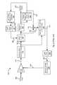
- FIG. 1depicts an existing timing recovery loop circuit
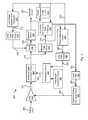
- FIG. 2depicts an existing automatic gain control loop circuit
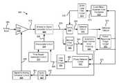
- FIG. 3depicts a combination automatic gain control loop and timing recovery loop circuit exhibiting semi-independence between a digital filter loop and the gain control and timing recovery loops in accordance with one or more embodiments of the present invention
- FIG. 4shows a mimic filter circuit in accordance with some embodiments of the present invention that may be used in place of the mimic filter circuit of FIG. 3 ;
- FIG. 5is a flow diagram showing a method for semi-independent loop processing in accordance with various embodiments of the present invention.
- FIG. 6shows a storage system including a read channel circuit with semi-independent loop circuits in accordance with some embodiments of the present invention.
- FIG. 7depicts a wireless communication system including semi-independent loop circuits in accordance with some embodiments of the present invention.
- the present inventionsare related to systems and methods for data processing, and more particularly to systems and methods for loop processing.
- Timing recovery loop circuit 100includes an analog to digital converter circuit 110 that converts an analog input signal 105 into a series of digital samples 115 that are provided to a digital finite impulse response (DFIR) filter 120 .
- DFIR filter 120filters the received input and provides a corresponding filtered output 125 to both a detector circuit 130 and a phase detector circuit 150 .
- Detector circuit 130performs a data detection process on the received input resulting in a detected output 135 . In performing the detection process, detector circuit 130 attempts to correct any errors in the received data input.
- Detected output 135is provided to a partial response target circuit 140 that creates a partial response output 145 compatible with filtered output 125 .
- Detected output 135is also provided to a least mean squared error generator circuit 190 that provides an error output 192 to a loop filter circuit 195 .
- the least mean squared error generator circuitis one type of error generator circuit that may be used in relation to different embodiments of the present invention. Based upon the disclosure provided herein, one of ordinary skill in the art will recognize other types of error generator circuits that may be used in relation to different embodiments of the present invention. For example, a zero forcing error generator circuit or a hybrid zero forcing error generator circuit and least mean squared error generator circuit may be used in place of least mean squared error generator circuit 190 .
- DFIR loop filter circuit 195provides a filtered output 197 (i.e., filter taps) to DFIR circuit 120 . The operation of DFIR circuit 120 is governed at least in part by filtered output 197 .
- Phase detector circuit 150determines a phase difference between partial response output 145 and filtered output 125 and yields a phase error output 155 .
- phase error output 155goes to zero.
- Phase error output 155is provided to a loop filter circuit 160 that filters the received input and provides a corresponding filtered output 165 .
- Filtered output 165is provided to an interpolator circuit 170 that is operable to determine an optimal sampling phase/frequency for a sampling clock 175 .
- Sampling clock 175is based on a clock input provided by a time based generator circuit 180 .
- the next instance of analog input 105is sampled by analog to digital converter circuit 110 synchronous to sampling clock 175 .
- timing recovery loop circuit 100uses filtered output 125 to generate both filtered output 197 provided to DFIR circuit 120 and sampling clock 175 .
- filtered output 197effects sampling clock 175 and sampling clock 175 effects filtered output 197
- filtered output 197may be constrained. Further, the interaction can cause a change in the transfer function of DFIR circuit 120 resulting in sub-optimal operation of DFIR circuit 120 .
- FIG. 2depicts an existing automatic gain control loop circuit 200 .
- Automatic gain control loop circuit 200includes a variable gain amplifier 210 that receives an analog input 205 .
- Variable gain amplifier 210amplifies analog input 205 to yield an amplified output 215 that is provided to an analog to digital converter circuit 220 .
- Analog to digital converter circuit 220converts the received signal into a series of digital samples 225 that are provided to a DFIR circuit 240 .
- DFIR circuit 240filters the received input and provides a corresponding filtered output 245 .
- digital samples 225are provided to an automatic gain control error forming circuit 230 .
- Filtered output 245is provided to both a detector circuit 250 and a summation circuit 270 .
- Detector circuit 250performs a data detection process on the received input resulting in a detected output 256 . In performing the detection process, detector circuit 250 attempts to correct any errors in the received data input.
- Detected output 256is provided to a partial response target circuit 260 that creates a partial response output 265 compatible with filtered output 245 .
- Summation circuit 270subtracts partial response output 265 from filtered output 245 to yield an error value 275 .
- Error value 275is provided to automatic gain control error forming circuit 230 where it is used to modify digital samples to yield an error feedback signal 255 .
- Error feedback signal 255is provided to a loop filter circuit 280 that filters the received input and provides a filtered output 285 to a digital to analog converter circuit 290 .
- Digital to analog converter circuit 290converts the received input to feedback signal 295 .
- Feedback signal 295governs the level of amplification applied by variable gain amplifier circuit 210 .
- Detected output 256is also provided to a least mean squared error generator circuit 288 that provides an error output 292 to a loop filter circuit 294 .
- the least mean squared error generator circuitis one type of error generator circuit that may be used in relation to different embodiments of the present invention. Based upon the disclosure provided herein, one of ordinary skill in the art will recognize other types of error generator circuits that may be used in relation to different embodiments of the present invention. For example, a zero forcing error generator circuit or a hybrid zero forcing error generator circuit and least mean squared error generator circuit may be used in place of least mean squared error generator circuit 288 .
- DFIR loop filter circuit 294provides a filtered output 296 (i.e., filter taps) to DFIR circuit 240 . The operation of DFIR circuit 240 is governed at least in part by filtered output 296 .
- timing recovery loop circuit 200uses filtered output 225 to generate both filtered output 296 provided to DFIR circuit 240 and feedback signal 295 .
- filtered output 296effects feedback signal 295 and feedback signal 295 effects filtered output 296
- the loopswill be unstable.
- filtered output 296may be constrained. Further, the interaction can cause a change in the transfer function of DFIR circuit 240 resulting in sub-optimal operation of DFIR circuit 240 .
- Various embodiments of the present inventionprovide data processing circuits that utilize semi-independent loop circuits limiting interaction between competing loop circuits and thus yielding greater loop stability.
- some embodiments of the presentprovide a data processing circuit with a combination timing recovery loop, automatic gain control loop and DFIR adaption loop circuit.
- the aforementioned loop circuitsare semi-independent allowing for increased stability of operation.
- a mimicking circuitis employed to decouple the semi-dependent feedback loops.
- Circuit 300includes a variable gain amplifier 310 that receives an analog input 305 .
- Variable gain amplifier 310may be any circuit known in the art that is capable of amplifying a received signal by a gain that can be changed. Based upon the disclosure provided herein, one of ordinary skill in the art will recognize a variety of circuits that may be used to implement variable gain amplifier 310 .
- Analog input 305may be any analog signal carrying information to be processed. In some embodiments of the present invention, analog input 305 is derived from a storage medium.
- analog input 305is derived from a transmission device. Based upon the disclosure provided herein, one of ordinary skill in the art will recognize a variety of analog signals and/or sources thereof that may be used in relation to different embodiments of the present invention.
- Variable gain amplifier 310amplifies analog input 305 to yield an amplified output 315 that is provided to an analog to digital converter circuit 320 .
- Analog to digital converter circuit 320may be any circuit known in the art that is capable of converting an analog signal into a series of digital values representing the received analog signal. Analog to digital converter circuit 320 converts the received amplified output 315 into a series of digital samples 325 that are provided to a DFIR circuit 330 . DFIR circuit 330 may be any circuit known in the art for filtering a digital signal. DFIR circuit 330 filters the received digital samples 325 and provides a corresponding filtered output 335 to a detector circuit 340 . Detector circuit 340 may be any detector circuit known in the art including, but not limited to, a Viterbi algorithm detector circuit or a maximum a posteriori detector circuit.
- Detector circuit 340performs a data detection process on the received input resulting in a detected output 345 .
- Detected output 345may be provided to a downstream processor (not shown) that performs additional processing on the output.
- detected output 345is provided to a partial response target circuit 370 that creates a partial response output 375 .
- Partial response output 375is provided to a least mean squared error generator circuit 372 that provides an error output 373 to a DFIR loop filter circuit 374 .
- the least mean squared error generator circuitis one type of error generator circuit that may be used in relation to different embodiments of the present invention. Based upon the disclosure provided herein, one of ordinary skill in the art will recognize other types of error generator circuits that may be used in relation to different embodiments of the present invention. For example, a zero forcing error generator circuit or a hybrid zero forcing error generator circuit and least mean squared error generator circuit may be used in place of least mean squared error generator circuit 372 .
- DFIR loop filter circuit 374provides a filtered output 376 (i.e., filter taps) to DFIR circuit 240 . The operation of DFIR circuit 330 is governed at least in part by filtered output 376 .
- Mimic filter circuit 350operates to provide a reasonable approximation of filtered output 335 , while not reacting immediately to changes in filtered output 376 that governs the operation of DFIR circuit 330 .
- Mimic circuit 350provides a mimicked output 355 to an automatic gain control error forming circuit 360 .
- partial response output 375is provided to automatic gain control error forming circuit 360 .
- Automatic gain control error forming circuit 360may be any circuit known in the art that is capable combining a post detector signal with a pre-detector signal to yield a gain control feedback compatible with a variable gain amplifier circuit.
- Automatic gain control error forming circuit 360provides a gain control feedback signal 335 to a loop filter circuit 362 where it is filtered and provided as a filtered output 364 .
- Filtered output 364is provided to a digital to analog converted circuit 366 that converts the received signal into a corresponding analog feedback signal 368 that adjusts the magnitude of the amplification applied by variable gain amplifier circuit 310 .
- Mimicked output 355is also provided to a phase detector circuit 380 that compares the phase difference between mimicked output 355 and partial response output 375 .
- Phase detector circuit 380may be any circuit known in the art that is capable of detecting a phase difference between two signals and providing an output corresponding to the phase difference.
- Phase detector circuit 380provide a phase difference output 385 .
- Phase difference output 385is filtered by a loop filter circuit 390 that provides a filtered output 395 to an interpolator circuit 324 .
- Interpolator circuit 324is operable to determine an optimal sampling phase/frequency for a sampling clock 326 .
- Interpolator circuit 324may be any circuit known in the art that is capable of identifying a point between two samples that is appropriate for sampling future samples.
- Sampling clock 326is based on a clock input provided by a time based generator circuit 322 .
- the next instance of analog input 305is sampled by analog to digital converter circuit 310 synchronous to sampling clock 326 .
- analog input signal 305is received.
- the analog input signalis derived from a storage medium.
- the analog input signalis derived from a transmission medium. Based upon the disclosure provided herein, one of ordinary skill in the art will recognize other sources from which the analog input signal may be derived.
- Analog input 305is provided to a variable gain amplifier circuit 310 where it is amplified to yield amplified output 315 .
- Amplified output 315is converted to a series of digital samples 325 synchronous to a sample clock 326 .
- DFIR circuit 330applies digital filtering to digital samples 325 to yield filtered output 335 .
- Filtered output 335is provided to detector circuit 340 that performs a data detection process on the received input and provides detected output 345 .
- Partial response target circuit 370convolves detected output 345 with a target to yield partial response output 375 .
- a least mean squared erroris generated using partial response output 375 by least mean squared error generator circuit 372 , and error output 373 is filtered by DFIR loop filter circuit 374 to yield filtered output 376 to DFIR circuit 330 .
- Processing from digital samples 325 through DFIR circuit 330 , detector circuit 340 , partial response target circuit 370 , least mean squared error generator circuit 372 and DFIR loop filter circuit 374 yielding filtered output 376is a DFIR adaptation loop.
- mimic filter circuit 350performs a filtering on digital samples 325 that approximates the filtering performed by DIFR circuit 330 to yield mimicked output 355 .
- Mimicked output 355is provided to phase detector circuit 380 that provides a phase difference between mimicked output 355 and partial response output 375 to a loop filter circuit 390 .
- the filtered output from loop filter circuit 390is interpolated using interpolator circuit 324 to yield sample clock 326 .
- Processing from digital samples 325 through mimic filter circuit 350 , phase detector circuit 380 , loop filter circuit 390 and interpolator circuit 324 yielding sample clock 326is a timing recovery loop.
- the timing recovery loopoperates semi-independent from the DFIR adaptation loop.
- mimicked output 355is provided to automatic gain control forming error circuit 360 that calculates an error difference between mimicked output 355 and partial response output 375 .
- the calculated erroris filtered and converted to analog feedback signal 368 that at least in part governs the magnitude of the amplification applied by variable gain amplifier circuit 310 .
- Processing from digital samples 325 through mimic filter circuit 350 , automatic gain control error forming circuit 360 , loop filter circuit 362 , and digital to analog converter circuit 366 to yield analog feedback signal 368is an automatic gain control loop.
- the automatic gain control loopoperates semi-independent from the DFIR adaptation loop.
- Mimic filter circuit 400includes a phase shift filter circuit 410 provides a phase shift output 415 .
- Phase shift output 415is provided to a magnitude test and set circuit 420 that compares the received input to a threshold value, and provides a set output 425 based upon the result of the comparison.
- magnitude test and set circuit 420operates in accordance with the following pseudocode:
- Set output 425is provided to a high frequency boost circuit 430 that provides a boosted output 435 to a summation circuit 440 .
- High frequency boost circuit 430operates to amplify high frequency components of a signal and leave low frequency components unmodified.
- the combination of phase shift filter circuit 410 , magnitude test and set circuit 420 , and high frequency boost circuit 430operate as a high pass filter circuit that amplifies frequencies above a frequency threshold.
- mimic filter circuit 400includes a delay circuit 450 that delays a received signal and provided a delayed signal 465 to a magnitude test and set circuit 470 .
- Magnitude test and set circuit 470provides a set output 475 to summation circuit 440 .
- Magnitude test and set circuit 470compares the received input to a threshold value, and provides set output 475 in accordance with the following pseudocode:
- the value of the threshold variableis the same as that used in magnitude test and set circuit 420 .
- the delay imposed by delay circuit 450is designed to match the latency through phase shift filter circuit 410 and high frequency boost circuit 430 , and thus aligning set output 475 with boosted output 435 (assuming the latency through magnitude test and set circuit 420 is approximately the same as the latency through magnitude test and set circuit 470 ).
- the combination of delay circuit 450 and magnitude test and set circuit 470operate as a low pass filter circuit that amplifies frequencies above a frequency threshold.
- an input 405is received.
- input 405is a series of digital samples provided from an analog to digital converter circuit.
- Input 405is high pass filtered through the combination of phase shift filter circuit 410 , magnitude test and set circuit 420 , and high frequency boost circuit 430 to yield boosted output 435 .
- input 405is low pass filtered by the combination of delay circuit 450 and magnitude test and set circuit 470 to yield set output 475 .
- Set output 475is added to boosted output 435 to yield a high frequency boosted output 485 .
- mimic filter circuit 400is similar to that of DFIR circuit 330 except that it does not react quickly to any changes in filtered output 376 . Rather, mimic filter circuit 400 only indirectly reacts to changes in filtered output 376 after the effect of filtered output 376 on DFIR circuit 330 is allowed to propagated through detector circuit 340 and then be formatted as the respective feedback signals. This results in semi-independent loop circuits that enhance loop stability without requiring limitations on the range of filtered output 376 .
- a flow diagram 700shows a method for semi-independent loop processing in accordance with various embodiments of the present invention.
- an analog input signalis received (block 775 ).
- the analog input signalis derived from a storage medium.
- the analog input signalis derived from a transmission medium. Based upon the disclosure provided herein, one of ordinary skill in the art will recognize other sources from which the analog input signal may be derived.
- a variable gain amplificationis applied to the received analog input signal to yield an amplified analog input signal (block 780 ).
- the magnitude of the amplification applied by the variable gain amplificationis governed at least in part by an amplifier feedback signal.
- An analog to digital conversionis performed on the amplified analog input to yield a series of digital samples (block 715 ).
- the digital samplesare generated synchronous to a sample clock that is adjusted based upon feedback from previous processing.
- Digital filteringis applied to the digital data samples to yield a filtered output (block 720 ).
- the digital filteringis done by a digital finite impulse response circuit as is known in the art.
- a data detection processis then applied to the filtered output to yield a detected output (block 725 ).
- the detection processmay be any data detection process known in the art including, but not limited to, a Viterbi algorithm detection process or a maximum a posteriori detection process.
- the resulting detected outputis provided both as an output to an upstream processing circuit (block 745 ) and to a convolution filter circuit (block 730 ).
- the convolution filter circuitconvolves the detected output with a partial response target to yield a target output. Using the target output, a least mean squared error is generated and the error is filtered to yield a DFIR feedback signal that at least in part governs the operation of the digital filtering performed in block 720 (block 770 ).
- a mimicked filtering of the digital data samples from block 715is performed to yield a mimicked output (block 740 ). In some cases, this includes performing a function on the received digital data samples that approximates the filtering function applied in block 720 , but without reacting directly to the feedback provided to block 720 .
- the mimicked filteringincludes performing a low pass filtering of the digital data samples to yield a low pass output and a high pass filtering of the digital data samples including an amplification of the high frequency components of the digital data samples to yield a boosted high pass signal. The boosted high pass signal is then summed with the low pass signal to yield the mimicked output.
- a phase difference detectionis performed to determine a phase difference between the mimicked output and the target output (block 750 ).
- the phase erroris then filtered and interpolated, with the output of the interpolation process being used to provide a feedback signal (i.e., a sampling clock) that is used in the analog to digital conversion process of block 715 (block 755 ).
- a gain erroris calculated based upon the target output and the mimicked output (block 760 ).
- the gain erroris then filtered and converted from the digital domain to the analog domain to yield an analog gain feedback signal (block 765 ).
- the gain feedback signalat least in part governs the magnitude of the amplification applied by the variable gain amplification of block 780 .
- blocks 720 , 725 , 730 , 770is a DFIR adaptation loop
- blocks 720 , 725 , 730 , 740 , 760 , 765 , 780 , 715is an automatic gain control loop
- blocks 720 , 725 , 730 , 740 , 750 , 755 , 715is a timing recovery loop.
- both the automatic gain control loop and the timing recovery loopoperate semi-independently as they are not directly impacted by the DFIR feedback of block 770 .
- FIG. 6shows a storage system 500 including a read channel circuit 510 with semi-independent loop circuits in accordance with some embodiments of the present invention.
- Storage system 500may be, for example, a hard disk drive.
- Storage system 500also includes a preamplifier 570 , an interface controller 520 , a hard disk controller 566 , a motor controller 568 , a spindle motor 572 , a disk platter 578 , and a read/write head assembly 576 .
- Interface controller 520controls addressing and timing of data to/from disk platter 578 .
- the data on disk platter 578consists of groups of magnetic signals that may be detected by read/write head assembly 576 when the assembly is properly positioned over disk platter 578 .
- disk platter 578includes magnetic signals recorded in accordance with either a longitudinal or a perpendicular recording scheme.
- read/write head assembly 576is accurately positioned by motor controller 568 over a desired data track on disk platter 578 .
- Motor controller 568both positions read/write head assembly 576 in relation to disk platter 578 and drives spindle motor 572 by moving read/write head assembly to the proper data track on disk platter 578 under the direction of hard disk controller 566 .
- Spindle motor 572spins disk platter 578 at a determined spin rate (RPMs).
- the sensed magnetic signalsare provided as a continuous, minute analog signal representative of the magnetic data on disk platter 578 .
- This minute analog signalis transferred from read/write head assembly 576 to read channel circuit 510 via preamplifier 570 .
- Preamplifier 570is operable to amplify the minute analog signals accessed from disk platter 578 .
- read channel circuit 510decodes and digitizes the received analog signal to recreate the information originally written to disk platter 578 .
- This datais provided as read data 503 to a receiving circuit.
- read channel circuit 510processes the received signal using a data processing circuit including semi-independent loops similar to that discussed above in relation to FIGS. 3-5 .
- a write operationis substantially the opposite of the preceding read operation with write data 501 being provided to read channel circuit 510 . This data is then encoded and written to disk platter 578 .
- storage system 500may be integrated into a larger storage system such as, for example, a RAID (redundant array of inexpensive disks or redundant array of independent disks) based storage system. It should also be noted that various functions or blocks of storage system 500 may be implemented in either software or firmware, while other functions or blocks are implemented in hardware.
- RAIDredundant array of inexpensive disks or redundant array of independent disks
- Communication system 600includes a transmitter 610 that is operable to transmit encoded information via a transfer medium 630 as is known in the art.
- the encoded datais received from transfer medium 630 by receiver 620 .
- Receiver 620incorporates semi-independent loop circuits similar to that discussed above in relation to FIGS. 3-5 .
- Such integrated circuitsmay include all of the functions of a given block, system or circuit, or only a subset of the block, system or circuit. Further, elements of the blocks, systems or circuits may be implemented across multiple integrated circuits. Such integrated circuits may be any type of integrated circuit known in the art including, but are not limited to, a monolithic integrated circuit, a flip chip integrated circuit, a multichip module integrated circuit, and/or a mixed signal integrated circuit. It should also be noted that various functions of the blocks, systems or circuits discussed herein may be implemented in either software or firmware. In some such cases, the entire system, block or circuit may be implemented using its software or firmware equivalent. In other cases, the one part of a given system, block or circuit may be implemented in software or firmware, while other parts are implemented in hardware.
Landscapes
- Engineering & Computer Science (AREA)
- Theoretical Computer Science (AREA)
- Analogue/Digital Conversion (AREA)
Abstract
Description
where ‘1’ represents the current sample phase, and D represents a storage element.
| If (| | ||
| { | ||
| } | |
| Else | |
| { |
| Set |
| } | ||
The value of the threshold variable may be programmable or fixed depending upon the particular implementation.
| If (| | ||
| { | ||
| } | |
| Else | |
| { |
| Set |
| } | ||
The value of the threshold variable is the same as that used in magnitude test and set circuit420. The delay imposed by delay circuit450 is designed to match the latency through phase
Claims (22)
Priority Applications (1)
| Application Number | Priority Date | Filing Date | Title |
|---|---|---|---|
| US12/887,327US8237597B2 (en) | 2010-09-21 | 2010-09-21 | Systems and methods for semi-independent loop processing |
Applications Claiming Priority (1)
| Application Number | Priority Date | Filing Date | Title |
|---|---|---|---|
| US12/887,327US8237597B2 (en) | 2010-09-21 | 2010-09-21 | Systems and methods for semi-independent loop processing |
Publications (2)
| Publication Number | Publication Date |
|---|---|
| US20120068870A1 US20120068870A1 (en) | 2012-03-22 |
| US8237597B2true US8237597B2 (en) | 2012-08-07 |
Family
ID=45817254
Family Applications (1)
| Application Number | Title | Priority Date | Filing Date |
|---|---|---|---|
| US12/887,327Expired - Fee RelatedUS8237597B2 (en) | 2010-09-21 | 2010-09-21 | Systems and methods for semi-independent loop processing |
Country Status (1)
| Country | Link |
|---|---|
| US (1) | US8237597B2 (en) |
Cited By (81)
| Publication number | Priority date | Publication date | Assignee | Title |
|---|---|---|---|---|
| US8451158B2 (en) | 2011-06-30 | 2013-05-28 | Lsi Corporation | Analog to digital converter with generalized beamformer |
| US8522120B2 (en) | 2009-06-24 | 2013-08-27 | Lsi Corporation | Systems and methods for out of order Y-sample memory management |
| US8566666B2 (en) | 2011-07-11 | 2013-10-22 | Lsi Corporation | Min-sum based non-binary LDPC decoder |
| US8564897B1 (en) | 2012-06-21 | 2013-10-22 | Lsi Corporation | Systems and methods for enhanced sync mark detection |
| US8595576B2 (en) | 2011-06-30 | 2013-11-26 | Lsi Corporation | Systems and methods for evaluating and debugging LDPC iterative decoders |
| US8612826B2 (en) | 2012-05-17 | 2013-12-17 | Lsi Corporation | Systems and methods for non-binary LDPC encoding |
| US8610608B2 (en) | 2012-03-08 | 2013-12-17 | Lsi Corporation | Systems and methods for reduced latency loop correction |
| US8625216B2 (en) | 2012-06-07 | 2014-01-07 | Lsi Corporation | Servo zone detector |
| US8625221B2 (en) | 2011-12-15 | 2014-01-07 | Lsi Corporation | Detector pruning control system |
| US8631300B2 (en) | 2011-12-12 | 2014-01-14 | Lsi Corporation | Systems and methods for scalable data processing shut down |
| US8634152B1 (en) | 2012-10-15 | 2014-01-21 | Lsi Corporation | Systems and methods for throughput enhanced data detection in a data processing circuit |
| US8650451B2 (en) | 2011-06-30 | 2014-02-11 | Lsi Corporation | Stochastic stream decoding of binary LDPC codes |
| US8656249B2 (en) | 2011-09-07 | 2014-02-18 | Lsi Corporation | Multi-level LDPC layer decoder |
| US8661311B2 (en) | 2010-04-19 | 2014-02-25 | Lsi Corporation | Systems and methods for dynamic scaling in a data decoding system |
| US8681444B2 (en) | 2012-06-07 | 2014-03-25 | Lsi Corporation | Multi-zone servo processor |
| US8700981B2 (en) | 2011-11-14 | 2014-04-15 | Lsi Corporation | Low latency enumeration endec |
| US8707123B2 (en) | 2011-12-30 | 2014-04-22 | Lsi Corporation | Variable barrel shifter |
| US8719686B2 (en) | 2011-11-22 | 2014-05-06 | Lsi Corporation | Probability-based multi-level LDPC decoder |
| US8731115B2 (en) | 2012-03-08 | 2014-05-20 | Lsi Corporation | Systems and methods for data processing including pre-equalizer noise suppression |
| US8751915B2 (en) | 2012-08-28 | 2014-06-10 | Lsi Corporation | Systems and methods for selectable positive feedback data processing |
| US8749907B2 (en) | 2012-02-14 | 2014-06-10 | Lsi Corporation | Systems and methods for adaptive decoder message scaling |
| US8751889B2 (en) | 2012-01-31 | 2014-06-10 | Lsi Corporation | Systems and methods for multi-pass alternate decoding |
| US8756478B2 (en) | 2011-09-07 | 2014-06-17 | Lsi Corporation | Multi-level LDPC layer decoder |
| US8760991B2 (en) | 2011-11-14 | 2014-06-24 | Lsi Corporation | Systems and methods for post processing gain correction |
| US8760977B2 (en) | 2011-04-28 | 2014-06-24 | Lsi Corporation | Systems and methods for data write loopback based timing control |
| US8775896B2 (en) | 2012-02-09 | 2014-07-08 | Lsi Corporation | Non-binary LDPC decoder with low latency scheduling |
| US8773791B1 (en) | 2013-01-14 | 2014-07-08 | Lsi Corporation | Systems and methods for X-sample based noise cancellation |
| US8773811B2 (en) | 2011-12-12 | 2014-07-08 | Lsi Corporation | Systems and methods for zone servo timing gain recovery |
| US8782486B2 (en) | 2012-03-05 | 2014-07-15 | Lsi Corporation | Systems and methods for multi-matrix data processing |
| US8788921B2 (en) | 2011-10-27 | 2014-07-22 | Lsi Corporation | Detector with soft pruning |
| US8797668B1 (en) | 2013-03-13 | 2014-08-05 | Lsi Corporation | Systems and methods for penalty based multi-variant encoding |
| US8819515B2 (en) | 2011-12-30 | 2014-08-26 | Lsi Corporation | Mixed domain FFT-based non-binary LDPC decoder |
| US8817404B1 (en) | 2013-07-18 | 2014-08-26 | Lsi Corporation | Systems and methods for data processing control |
| US8850295B2 (en) | 2012-02-01 | 2014-09-30 | Lsi Corporation | Symbol flipping data processor |
| US8862972B2 (en) | 2011-06-29 | 2014-10-14 | Lsi Corporation | Low latency multi-detector noise cancellation |
| US8873182B2 (en) | 2012-03-09 | 2014-10-28 | Lsi Corporation | Multi-path data processing system |
| US8880986B2 (en) | 2012-05-30 | 2014-11-04 | Lsi Corporation | Systems and methods for improved data detection processing |
| US8885276B2 (en) | 2013-02-14 | 2014-11-11 | Lsi Corporation | Systems and methods for shared layer data decoding |
| US8908307B1 (en) | 2013-08-23 | 2014-12-09 | Lsi Corporation | Systems and methods for hard disk drive region based data encoding |
| US8917466B1 (en) | 2013-07-17 | 2014-12-23 | Lsi Corporation | Systems and methods for governing in-flight data sets in a data processing system |
| US8930792B2 (en) | 2013-02-14 | 2015-01-06 | Lsi Corporation | Systems and methods for distributed low density parity check decoding |
| US8930780B2 (en) | 2012-08-28 | 2015-01-06 | Lsi Corporation | Systems and methods for non-zero syndrome based processing |
| US8929009B2 (en) | 2012-12-19 | 2015-01-06 | Lsi Corporation | Irregular low density parity check decoder with low syndrome error handling |
| US8949702B2 (en) | 2012-09-14 | 2015-02-03 | Lsi Corporation | Systems and methods for detector side trapping set mitigation |
| US8959414B2 (en) | 2013-06-13 | 2015-02-17 | Lsi Corporation | Systems and methods for hybrid layer data decoding |
| US8976475B1 (en) | 2013-11-12 | 2015-03-10 | Lsi Corporation | Systems and methods for large sector dynamic format insertion |
| US8977937B2 (en) | 2012-03-16 | 2015-03-10 | Lsi Corporation | Systems and methods for compression driven variable rate decoding in a data processing system |
| US9003263B2 (en) | 2013-01-15 | 2015-04-07 | Lsi Corporation | Encoder and decoder generation by state-splitting of directed graph |
| US9009557B2 (en) | 2013-01-21 | 2015-04-14 | Lsi Corporation | Systems and methods for reusing a layered decoder to yield a non-layered result |
| US9019641B2 (en) | 2012-12-13 | 2015-04-28 | Lsi Corporation | Systems and methods for adaptive threshold pattern detection |
| US9019647B2 (en) | 2012-08-28 | 2015-04-28 | Lsi Corporation | Systems and methods for conditional positive feedback data decoding |
| US9043684B2 (en) | 2012-03-22 | 2015-05-26 | Lsi Corporation | Systems and methods for variable redundancy data protection |
| US9048870B2 (en) | 2012-11-19 | 2015-06-02 | Lsi Corporation | Low density parity check decoder with flexible saturation |
| US9048867B2 (en) | 2013-05-21 | 2015-06-02 | Lsi Corporation | Shift register-based layered low density parity check decoder |
| US9047882B2 (en) | 2013-08-30 | 2015-06-02 | Lsi Corporation | Systems and methods for multi-level encoding and decoding |
| US9048873B2 (en) | 2013-03-13 | 2015-06-02 | Lsi Corporation | Systems and methods for multi-stage encoding of concatenated low density parity check codes |
| US9048874B2 (en) | 2013-03-15 | 2015-06-02 | Lsi Corporation | Min-sum based hybrid non-binary low density parity check decoder |
| US9053217B2 (en) | 2013-02-17 | 2015-06-09 | Lsi Corporation | Ratio-adjustable sync mark detection system |
| US9112531B2 (en) | 2012-10-15 | 2015-08-18 | Avago Technologies General Ip (Singapore) Pte. Ltd. | Systems and methods for enhanced local iteration randomization in a data decoder |
| US9129651B2 (en) | 2013-08-30 | 2015-09-08 | Avago Technologies General Ip (Singapore) Pte. Ltd. | Array-reader based magnetic recording systems with quadrature amplitude modulation |
| US9130590B2 (en) | 2013-09-29 | 2015-09-08 | Lsi Corporation | Non-binary layered low density parity check decoder |
| US9129650B2 (en) | 2013-07-25 | 2015-09-08 | Avago Technologies General Ip (Singapore) Pte. Ltd. | Array-reader based magnetic recording systems with frequency division multiplexing |
| US9129646B2 (en) | 2013-09-07 | 2015-09-08 | Avago Technologies General Ip (Singapore) Pte. Ltd. | Array-reader based magnetic recording systems with mixed synchronization |
| US9130599B2 (en) | 2013-12-24 | 2015-09-08 | Avago Technologies General Ip (Singapore) Pte. Ltd. | Systems and methods of converting detector output to multi-level soft information |
| US9130589B2 (en) | 2012-12-19 | 2015-09-08 | Avago Technologies General Ip (Singapore) Pte. Ltd. | Low density parity check decoder with dynamic scaling |
| US9196297B2 (en) | 2013-03-14 | 2015-11-24 | Avago Technologies General Ip (Singapore) Pte. Ltd. | Systems and methods for enhanced sync mark mis-detection protection |
| US9196299B2 (en) | 2013-08-23 | 2015-11-24 | Avago Technologies General Ip (Singapore) Pte. Ltd. | Systems and methods for enhanced data encoding and decoding |
| US9214959B2 (en) | 2013-02-19 | 2015-12-15 | Avago Technologies General Ip (Singapore) Pte. Ltd. | Systems and methods for skip layer data decoding |
| US9219503B2 (en) | 2013-10-16 | 2015-12-22 | Avago Technologies General Ip (Singapore) Pte. Ltd. | Systems and methods for multi-algorithm concatenation encoding and decoding |
| US9230596B2 (en) | 2012-03-22 | 2016-01-05 | Avago Technologies General Ip (Singapore) Pte. Ltd. | Systems and methods for variable rate coding in a data processing system |
| US9274889B2 (en) | 2013-05-29 | 2016-03-01 | Avago Technologies General Ip (Singapore) Pte. Ltd. | Systems and methods for data processing using global iteration result reuse |
| US9275655B2 (en) | 2013-06-11 | 2016-03-01 | Avago Technologies General Ip (Singapore) Pte. Ltd. | Timing error detector with diversity loop detector decision feedback |
| US9281843B2 (en) | 2013-03-22 | 2016-03-08 | Avago Technologies General Ip (Singapore) Pte. Ltd. | Systems and methods for reduced constraint code data processing |
| US9298720B2 (en) | 2013-09-17 | 2016-03-29 | Avago Technologies General Ip (Singapore) Pte. Ltd. | Systems and methods for fragmented data recovery |
| US9324372B2 (en) | 2012-08-28 | 2016-04-26 | Avago Technologies General Ip (Singapore) Pte. Ltd. | Systems and methods for local iteration randomization in a data decoder |
| US9323606B2 (en) | 2013-11-21 | 2016-04-26 | Avago Technologies General Ip (Singapore) Pte. Ltd. | Systems and methods for FAID follower decoding |
| US9331716B2 (en) | 2014-02-10 | 2016-05-03 | Avago Technologies General Ip (Singapore) Pte. Ltd. | Systems and methods for area efficient data encoding |
| US9378765B2 (en) | 2014-04-03 | 2016-06-28 | Seagate Technology Llc | Systems and methods for differential message scaling in a decoding process |
| US9385858B2 (en)* | 2013-02-20 | 2016-07-05 | Avago Technologies General Ip (Singapore) Pte. Ltd. | Timing phase estimation for clock and data recovery |
| US10152999B2 (en) | 2013-07-03 | 2018-12-11 | Avago Technologies International Sales Pte. Limited | Systems and methods for correlation based data alignment |
| US10256845B1 (en) | 2018-02-26 | 2019-04-09 | International Business Machines Corporation | Symbol timing recovery based on speculative tentative symbol decisions |
Families Citing this family (1)
| Publication number | Priority date | Publication date | Assignee | Title |
|---|---|---|---|---|
| US8669891B2 (en)* | 2011-07-19 | 2014-03-11 | Lsi Corporation | Systems and methods for ADC based timing and gain control |
Citations (126)
| Publication number | Priority date | Publication date | Assignee | Title |
|---|---|---|---|---|
| US3973183A (en) | 1971-08-20 | 1976-08-03 | Agency Of Industrial Science & Technology | Method and apparatus for detecting uneven magnetic field by a change in resistance of semiconductor element |
| US3973182A (en) | 1971-08-20 | 1976-08-03 | Agency Of Industrial Science & Technology | Method and apparatus for detecting uneven magnetic field by hall effect in semiconductor |
| US4024571A (en) | 1975-08-14 | 1977-05-17 | Rca Corporation | Synchronizing system employing burst crossover detection |
| US4777544A (en) | 1986-08-15 | 1988-10-11 | International Business Machine Corporation | Method and apparatus for in-situ measurement of head/recording medium clearance |
| US5130866A (en) | 1990-07-17 | 1992-07-14 | International Business Machines Corporation | Method and circuitry for in-situ measurement of transducer/recording medium clearance and transducer magnetic instability |
| US5220466A (en)* | 1991-05-21 | 1993-06-15 | International Business Machines Corporation | Method and apparatus for digital filter control in a partial-response maximum-likelihood disk drive system |
| US5237325A (en) | 1989-11-21 | 1993-08-17 | Klein Hans Christoph | Process and system for gathering and evaluating measured data |
| US5278703A (en) | 1991-06-21 | 1994-01-11 | Digital Equipment Corp. | Embedded servo banded format for magnetic disks for use with a data processing system |
| US5309357A (en) | 1992-01-28 | 1994-05-03 | Independent Scintillation Imaging Systems (Isis) Inc. | Scintillation data collecting apparatus and method |
| US5341249A (en) | 1992-08-27 | 1994-08-23 | Quantum Corporation | Disk drive using PRML class IV sampling data detection with digital adaptive equalization |
| US5377058A (en) | 1992-12-31 | 1994-12-27 | International Business Machines Corporation | Fly height servo control of read/write head suspension |
| US5384671A (en)* | 1993-12-23 | 1995-01-24 | Quantum Corporation | PRML sampled data channel synchronous servo detector |
| US5442492A (en)* | 1993-06-29 | 1995-08-15 | International Business Machines Corporation | Data recovery procedure using DC offset and gain control for timing loop compensation for partial-response data detection |
| US5521948A (en) | 1994-04-28 | 1996-05-28 | Sony Corporation | Frequency synthesizer |
| US5523902A (en) | 1993-10-25 | 1996-06-04 | Syquest Technology, Inc. | Servo burst pattern for removing offset caused by magnetic distortion and method associated therewith |
| US5594341A (en) | 1994-06-27 | 1997-01-14 | Varian Associates, Inc. | Nuclear magnetic resonance receiver, method and system |
| US5668679A (en) | 1995-12-21 | 1997-09-16 | Quantum Corporation | System for self-servowriting a disk drive |
| US5696639A (en) | 1995-05-12 | 1997-12-09 | Cirrus Logic, Inc. | Sampled amplitude read channel employing interpolated timing recovery |
| US5726818A (en)* | 1995-12-05 | 1998-03-10 | Cirrus Logic, Inc. | Magnetic disk sampled amplitude read channel employing interpolated timing recovery for synchronous detection of embedded servo data |
| US5781129A (en) | 1997-03-03 | 1998-07-14 | Motorola, Inc. | Adaptive encoder circuit for multiple data channels and method of encoding |
| US5787125A (en) | 1996-05-06 | 1998-07-28 | Motorola, Inc. | Apparatus for deriving in-phase and quadrature-phase baseband signals from a communication signal |
| US5798885A (en) | 1994-06-06 | 1998-08-25 | Fujitsu Limited | Head positioning control for disk apparatus using peak detection, polarity detection and sector mark detection |
| US5835295A (en) | 1996-11-18 | 1998-11-10 | Cirrus Logice, Inc. | Zero phase restart interpolated timing recovery in a sampled amplitude read channel |
| US5844920A (en) | 1996-11-07 | 1998-12-01 | Cirrus Logic, Inc. | Thermal asperity compensation using multiple sync marks for retroactive and split segment data synchronization in a magnetic disk storage system |
| US5852524A (en) | 1997-02-07 | 1998-12-22 | Cirrus Logic, Inc. | Sampled amplitude read channel for processing multiple data streams in a disc storage system |
| US5892632A (en) | 1996-11-18 | 1999-04-06 | Cirrus Logic, Inc. | Sampled amplitude read channel employing a residue number system FIR filter in an adaptive equalizer and in interpolated timing recovery |
| US5955783A (en) | 1997-06-18 | 1999-09-21 | Lsi Logic Corporation | High frequency signal processing chip having signal pins distributed to minimize signal interference |
| US5970104A (en) | 1997-03-19 | 1999-10-19 | Cadence Design Systems, Inc. | Method and apparatus for generating branch metrics and branch indices for convolutional code Viterbi decoders |
| US5986830A (en) | 1997-07-30 | 1999-11-16 | Cirrus Logic, Inc. | Read/write channel write precompensation system and method using one or more delay clocks |
| US5987562A (en) | 1996-03-08 | 1999-11-16 | Texas Instruments Incorporated | Waveform sampler and method for sampling a signal from a read channel |
| US6009549A (en) | 1997-05-15 | 1999-12-28 | Cirrus Logic, Inc. | Disk storage system employing error detection and correction of channel coded data, interpolated timing recovery, and retroactive/split-segment symbol synchronization |
| US6023383A (en) | 1996-03-19 | 2000-02-08 | Texas Instruments Incorporated | Error estimation circuit and method for providing a read channel error signal |
| US6037886A (en)* | 1998-04-01 | 2000-03-14 | Texas Instruments Incorporated | Method and apparatus for extracting band and error values from digital samples of an analog signal |
| US6069583A (en) | 1996-05-09 | 2000-05-30 | Agence Spatiale Europeene | Receiver for a navigation system, in particular a satellite navigation system |
| US6081397A (en) | 1997-04-08 | 2000-06-27 | International Business Machines Corporation | Method and apparatus for SID-to-SID period estimation |
| US6111712A (en) | 1998-03-06 | 2000-08-29 | Cirrus Logic, Inc. | Method to improve the jitter of high frequency phase locked loops used in read channels |
| US6208478B1 (en) | 1998-07-07 | 2001-03-27 | Texas Instruments Incorporated | Read clock interface for read channel device |
| US6215433B1 (en)* | 1999-06-29 | 2001-04-10 | Oak Technology, Inc. | DC insensitive clock generator for optical PRML read channel |
| US6278591B1 (en) | 1998-04-02 | 2001-08-21 | International Business Machines Corporation | Inverted merged MR head having plated notched first pole tip and self-aligned second pole tip |
| US20020001151A1 (en) | 2000-06-02 | 2002-01-03 | Lake Jeffrey H. | Method and apparatus for head fly height measurement |
| US6400518B1 (en) | 2000-11-01 | 2002-06-04 | International Business Machines Corporation | Magneto-resistive asymmetry correction circuit |
| US6404829B1 (en) | 1999-06-29 | 2002-06-11 | Oak Technology, Inc. | DC insensitive AGC circuit for optical PRML read channel |
| US6411452B1 (en) | 1997-03-11 | 2002-06-25 | Western Digital Technologies, Inc. | Disk drive employing read error tolerant sync mark detection |
| US6441661B1 (en) | 1998-06-30 | 2002-08-27 | Asahi Kasei Kabushiki Kaisha | PLL circuit |
| US20020150179A1 (en) | 1994-10-11 | 2002-10-17 | Maxtor Corporation | Synchronous detection of wide bi-phase coded servo information for disk drive |
| US20020176185A1 (en) | 2001-05-22 | 2002-11-28 | Seagate Technology Llc | Method and system for measuring fly height |
| US6490110B2 (en) | 2000-12-05 | 2002-12-03 | Cirrus Logic, Inc. | Servo data detection with improved phase shift tolerance |
| US20020181377A1 (en) | 2001-04-27 | 2002-12-05 | Masayoshi Nagata | Phase-change optical disk and optical disk apparatus |
| US6493162B1 (en) | 1997-12-05 | 2002-12-10 | Seagate Technology Llc | Frame synchronization for viterbi detector |
| US6519102B1 (en) | 2000-04-27 | 2003-02-11 | International Business Machines Corporation | Method and apparatus for implementing an in-situ digital harmonic computation facility for direct access storage device (DASD) |
| US6530060B1 (en) | 2000-02-08 | 2003-03-04 | Cirrus Logic, Inc. | Sampled amplitude read channel employing a post processor with a boundary error compensator which compensates for boundary error events in a split-field data sector |
| US20030095350A1 (en) | 2001-10-24 | 2003-05-22 | Viswanath Annampedu | Servo data detection in the presence or absence of radial incoherence using digital interpolators |
| US6603622B1 (en) | 2001-02-28 | 2003-08-05 | Western Digital Technologies, Inc. | Disk drive employing a sync mark detector comprising a matched filter and a dual polarity correlator |
| US6606048B1 (en) | 2000-11-16 | 2003-08-12 | Marvell International, Ltd. | Method and apparatus for equalizing the digital performance of multiple ADC's |
| US6633447B2 (en) | 2001-05-25 | 2003-10-14 | Infineon Technologies Ag | Method and apparatus for compensation of second order distortion |
| US6646822B1 (en) | 1995-05-12 | 2003-11-11 | Cirrus Logic, Inc. | Sampled amplitude read channel employing pipelined reads to reduce the gap between sectors |
| US6657802B1 (en) | 1999-04-16 | 2003-12-02 | Infineon Technologies Corporation | Phase assisted synchronization detector |
| US6775529B1 (en) | 2000-07-31 | 2004-08-10 | Marvell International Ltd. | Active resistive summer for a transformer hybrid |
| US6788484B2 (en) | 2000-12-07 | 2004-09-07 | Nec Corporation | PLL circuit, data detection circuit and disk apparatus |
| US20040179460A1 (en) | 2000-01-14 | 2004-09-16 | Shigeru Furumiya | Optical disc and optical disc address reading apparatus and method |
| US6813108B2 (en) | 2001-10-24 | 2004-11-02 | Agere Systems Inc. | Servo data detection in presence of radial incoherence using multiple data detectors |
| US6816328B2 (en) | 2000-06-20 | 2004-11-09 | Infineon Technologies North America Corp. | Pseudo-synchronous interpolated timing recovery for a sampled amplitude read channel |
| US6839014B2 (en) | 2001-06-27 | 2005-01-04 | Renesas Technology Corp. | One-chip microcomputer with analog-to-digital converter |
| US6856183B2 (en) | 2001-10-12 | 2005-02-15 | Agere Systems Inc. | Scheme to improve performance of timing recovery systems for read channels in a disk drive |
| US20050046982A1 (en) | 2003-08-29 | 2005-03-03 | Bo Liu | Method and implementation of in-situ absolute head medium spacing measurement |
| US6876511B2 (en) | 2002-08-30 | 2005-04-05 | Kabushiki Kaisha Toshiba | Disk drive and method of detecting servo address mark in the same |
| US6912099B2 (en) | 2003-05-13 | 2005-06-28 | Agere Systems Inc. | Maximum likelihood detection of asynchronous servo data employing interpolation |
| US20050157415A1 (en) | 2004-01-21 | 2005-07-21 | Chiang Taivie | Head polarity detection algorithm and apparatus |
| US20050243455A1 (en) | 2004-04-30 | 2005-11-03 | Viswanath Annampedu | Method and apparatus for improved address mark detection |
| US6963521B2 (en) | 2001-03-30 | 2005-11-08 | Sony Corporation | Disc drive apparatus |
| US6999257B2 (en) | 2001-01-31 | 2006-02-14 | Kabushiki Kaisha Toshiba | Magnetic disk drive with structure for avoiding DC magnetic disturbance on a disk surface |
| US6999264B2 (en) | 2002-12-27 | 2006-02-14 | Matsushita Electric Industrial Co., Ltd. | Methods for variable multi-pass servowriting and self-servowriting |
| US7002767B2 (en) | 2003-09-30 | 2006-02-21 | Agere Systems Inc. | Detection of recorded data employing interpolation with gain compensation |
| US7002761B1 (en) | 2003-03-27 | 2006-02-21 | Marvell International Ltd. | Demodulation compensation for spiral servo tracks in hard disk drives |
| US7038875B2 (en) | 2003-07-31 | 2006-05-02 | Seagate Technology Llc | Dynamic measurement of head media spacing modulation |
| US7054088B2 (en) | 2002-01-21 | 2006-05-30 | Fujitsu Limited | Information recording and reproducing apparatus and method, and signal decoding circuit for performing timing recovery |
| US7072137B2 (en) | 2002-06-11 | 2006-07-04 | Fujitsu Limited | Data read device, read method and circuit controlling read device |
| US7092462B2 (en) | 2003-01-14 | 2006-08-15 | Agere Systems Inc. | Asynchronous servo RRO detection employing interpolation |
| US7116504B1 (en) | 2003-03-25 | 2006-10-03 | Marvell International Ltd. | DC-offset compensation loops for magnetic recording system |
| US7126776B1 (en) | 2002-04-17 | 2006-10-24 | Western Digital Technologies, Inc. | Disk drive having a sector clock that is synchronized to the angular speed of the spindle motor |
| US7136250B1 (en) | 2003-03-25 | 2006-11-14 | Marvell International Ltd. | Detecting fly height of a head over a storage medium |
| US7154689B1 (en) | 2004-02-05 | 2006-12-26 | Maxtor Corporation | Apparatus for writing servo bursts on a disk with servo track pitch based on read element width and methods of manufacturing same |
| US7167328B2 (en) | 2004-12-17 | 2007-01-23 | Agere Systems Inc. | Synchronizing an asynchronously detected servo signal to synchronous servo demodulation |
| US7171608B2 (en)* | 2002-09-20 | 2007-01-30 | Matsushita Electric Industrial Co., Ltd. | Data playback equipment for playing back data recorded on a disk medium |
| US7180693B2 (en) | 2004-04-14 | 2007-02-20 | Agere Systems Inc. | Method and apparatus for maximum likelihood detection of data employing interpolation with compensation of signal asymmetry |
| US7187739B2 (en) | 2002-05-20 | 2007-03-06 | Via Technologies, Inc. | Timing recovery circuit |
| US7191382B2 (en) | 2003-06-02 | 2007-03-13 | Fujitsu Limited | Methods and apparatus for correcting data and error detection codes on the fly |
| US7193798B2 (en) | 2005-01-12 | 2007-03-20 | Agere Systems, Inc. | Method and apparatus for encoding and decoding a runout correction bit pattern of servo field |
| US7193544B1 (en) | 2004-09-08 | 2007-03-20 | Northrop Grumman Corporation | Parallel, adaptive delta sigma ADC |
| US20070064847A1 (en) | 2003-05-16 | 2007-03-22 | Klaus Gaedke | Dsp-based data recovery |
| US20070071152A1 (en) | 2005-09-26 | 2007-03-29 | Via Technologies Inc. | Method and circuit for timing recovery |
| US7199961B1 (en) | 2003-03-25 | 2007-04-03 | Marvell International Ltd. | Detecting fly height of a head over a storage medium |
| US7203013B1 (en) | 2004-07-26 | 2007-04-10 | Marvell International Ltd. | Method and apparatus for asymmetry correction in magnetic recording channels |
| US7206146B2 (en) | 2004-10-27 | 2007-04-17 | Hitachi Global Storage Technologies Netherlands B.V. | Biphase magnetic pattern detector using multiple matched filters for hard disk drive |
| US20070103805A1 (en) | 2003-11-18 | 2007-05-10 | Sony Corporation | Reproduction device and method, recording medium, and program |
| US20070104300A1 (en) | 2005-09-22 | 2007-05-10 | Atsushi Esumi | Signal processing apparatus, signal processing method and storage system |
| US7230789B1 (en) | 2004-04-08 | 2007-06-12 | Maxtor Corporation | Method and apparatus for performing a self-servo write operation in a disk drive using spiral servo information |
| US7248425B2 (en) | 2004-12-14 | 2007-07-24 | Samsung Electronics Co., Ltd. | Disk writing/reproducing apparatus and method |
| US7253984B1 (en) | 2004-09-02 | 2007-08-07 | Maxtor Corporation | Disk drive that generates a position error signal and a fly height signal from a servo burst pattern |
| US20070183073A1 (en) | 2003-09-23 | 2007-08-09 | Pantas Sutardja | Timing Recovery for Data Storage Channels with Buffered Sectors |
| US7265937B1 (en) | 2006-06-09 | 2007-09-04 | Seagate Technology Llc | Positioning of a head array over a data storage medium |
| US20070230015A1 (en) | 2006-03-28 | 2007-10-04 | Fujitsu Limited | Storage device, control method, control device, and program |
| US20070263311A1 (en) | 2006-05-11 | 2007-11-15 | Smith Steven C | Position determination using circular shift codes |
| US7301717B1 (en) | 2004-07-30 | 2007-11-27 | Western Digital Technologies, Inc. | Servo writing a disk drive by integrating a spiral track read signal |
| US7308057B1 (en) | 2003-06-05 | 2007-12-11 | Maxtor Corporation | Baseline wander compensation for perpendicular recording |
| FR2904168A1 (en) | 2006-07-18 | 2008-01-25 | Thales Sa | SYSTEM FOR ESTIMATING THE RECEPTION QUALITY OF A DIGITAL TRANSMISSION. |
| US7323916B1 (en) | 2005-12-07 | 2008-01-29 | Netlogic Microsystems, Inc. | Methods and apparatus for generating multiple clocks using feedback interpolation |
| US20080056403A1 (en) | 2006-09-01 | 2008-03-06 | On Demand Microelectronics | Method and apparatus for timing recovery of pam signals |
| US20080080082A1 (en) | 2006-09-28 | 2008-04-03 | Seagate Technology Llc | Synchronization for data communication |
| US7362536B1 (en) | 2005-07-08 | 2008-04-22 | Maxtor Corporation | Disk drive that compensates for phase incoherence between radially adjacent servo tracks and methods thereof |
| US7375918B1 (en) | 2002-04-23 | 2008-05-20 | Maxtor Corporation | Method of self-servo writing in a disk drive using multiple timing windows |
| US7411531B2 (en) | 2006-06-30 | 2008-08-12 | Agere Systems Inc. | Methods and apparatus for asynchronous sampling of a received signal at a downsampled rate |
| US7420498B2 (en) | 2006-11-22 | 2008-09-02 | Infineon Technologies Ag | Signal converter performing a role |
| US20080212715A1 (en) | 2006-10-06 | 2008-09-04 | Yuan-Shuo Chang | Method and apparatus for baseline wander compensation in Ethernet application |
| US7423827B2 (en) | 2006-04-20 | 2008-09-09 | Agere Systems Inc. | Systems and methods for accessing data from a variable polarity head assembly |
| US20080266693A1 (en) | 2007-04-30 | 2008-10-30 | Broadcom Corporation | Base line control electronics architecture |
| US7446690B2 (en) | 2006-11-06 | 2008-11-04 | Atmel Corporation | Apparatus and method for implementing an analog-to-digital converter in programmable logic devices |
| US20090002862A1 (en) | 2007-06-28 | 2009-01-01 | Jongseung Park | Feed-forward dc restoration in a perpendicular magnetic read channel |
| US7499238B2 (en) | 2006-09-22 | 2009-03-03 | Agere Systems Inc. | Systems and methods for improving disk drive synchronization |
| US7525460B1 (en) | 2006-07-13 | 2009-04-28 | Marvell International Ltd. | Timing loop based on analog to digital converter output and method of use |
| US20090142620A1 (en) | 2004-06-22 | 2009-06-04 | Kabushiki Kaisha Toshiba | Magnetic recording medium, method of manufacturing the same, and magnetic recording/reproducing apparatus |
| US20090245448A1 (en) | 2008-03-28 | 2009-10-01 | Adee Ran | Adaptation of a digital receiver |
| US7602568B1 (en) | 2006-02-24 | 2009-10-13 | Marvell International Ltd. | Synchronous RRO write |
| US20090274247A1 (en) | 2008-04-30 | 2009-11-05 | Richard Leo Galbraith | Detection of synchronization mark from output of matched filter upstream of viterbi detector |
| US7620101B1 (en) | 2003-09-24 | 2009-11-17 | Cypress Semiconductor Corporation | Equalizer circuit, communication system, and method that is adaptive to varying launch amplitudes for reducing receiver error |
| US7630155B2 (en) | 2006-03-23 | 2009-12-08 | Fujitsu Limited | Eccentricity correction method, signal processing circuit, magnetic storage apparatus and perpendicular magnetic recording medium |
- 2010
- 2010-09-21USUS12/887,327patent/US8237597B2/ennot_activeExpired - Fee Related
Patent Citations (128)
| Publication number | Priority date | Publication date | Assignee | Title |
|---|---|---|---|---|
| US3973183A (en) | 1971-08-20 | 1976-08-03 | Agency Of Industrial Science & Technology | Method and apparatus for detecting uneven magnetic field by a change in resistance of semiconductor element |
| US3973182A (en) | 1971-08-20 | 1976-08-03 | Agency Of Industrial Science & Technology | Method and apparatus for detecting uneven magnetic field by hall effect in semiconductor |
| US4024571A (en) | 1975-08-14 | 1977-05-17 | Rca Corporation | Synchronizing system employing burst crossover detection |
| US4777544A (en) | 1986-08-15 | 1988-10-11 | International Business Machine Corporation | Method and apparatus for in-situ measurement of head/recording medium clearance |
| US5237325A (en) | 1989-11-21 | 1993-08-17 | Klein Hans Christoph | Process and system for gathering and evaluating measured data |
| US5130866A (en) | 1990-07-17 | 1992-07-14 | International Business Machines Corporation | Method and circuitry for in-situ measurement of transducer/recording medium clearance and transducer magnetic instability |
| US5220466A (en)* | 1991-05-21 | 1993-06-15 | International Business Machines Corporation | Method and apparatus for digital filter control in a partial-response maximum-likelihood disk drive system |
| US5278703A (en) | 1991-06-21 | 1994-01-11 | Digital Equipment Corp. | Embedded servo banded format for magnetic disks for use with a data processing system |
| US5309357A (en) | 1992-01-28 | 1994-05-03 | Independent Scintillation Imaging Systems (Isis) Inc. | Scintillation data collecting apparatus and method |
| US5341249A (en) | 1992-08-27 | 1994-08-23 | Quantum Corporation | Disk drive using PRML class IV sampling data detection with digital adaptive equalization |
| US5422760A (en)* | 1992-08-27 | 1995-06-06 | Quantum Corp. | Disk drive method using zoned data recording and PRML sampling data detection with digital adaptive equalization |
| US5377058A (en) | 1992-12-31 | 1994-12-27 | International Business Machines Corporation | Fly height servo control of read/write head suspension |
| US5442492A (en)* | 1993-06-29 | 1995-08-15 | International Business Machines Corporation | Data recovery procedure using DC offset and gain control for timing loop compensation for partial-response data detection |
| US5523902A (en) | 1993-10-25 | 1996-06-04 | Syquest Technology, Inc. | Servo burst pattern for removing offset caused by magnetic distortion and method associated therewith |
| US5384671A (en)* | 1993-12-23 | 1995-01-24 | Quantum Corporation | PRML sampled data channel synchronous servo detector |
| US5521948A (en) | 1994-04-28 | 1996-05-28 | Sony Corporation | Frequency synthesizer |
| US5798885A (en) | 1994-06-06 | 1998-08-25 | Fujitsu Limited | Head positioning control for disk apparatus using peak detection, polarity detection and sector mark detection |
| US5594341A (en) | 1994-06-27 | 1997-01-14 | Varian Associates, Inc. | Nuclear magnetic resonance receiver, method and system |
| US20020150179A1 (en) | 1994-10-11 | 2002-10-17 | Maxtor Corporation | Synchronous detection of wide bi-phase coded servo information for disk drive |
| US6646822B1 (en) | 1995-05-12 | 2003-11-11 | Cirrus Logic, Inc. | Sampled amplitude read channel employing pipelined reads to reduce the gap between sectors |
| US5696639A (en) | 1995-05-12 | 1997-12-09 | Cirrus Logic, Inc. | Sampled amplitude read channel employing interpolated timing recovery |
| US5726818A (en)* | 1995-12-05 | 1998-03-10 | Cirrus Logic, Inc. | Magnetic disk sampled amplitude read channel employing interpolated timing recovery for synchronous detection of embedded servo data |
| US5668679A (en) | 1995-12-21 | 1997-09-16 | Quantum Corporation | System for self-servowriting a disk drive |
| US5987562A (en) | 1996-03-08 | 1999-11-16 | Texas Instruments Incorporated | Waveform sampler and method for sampling a signal from a read channel |
| US6023383A (en) | 1996-03-19 | 2000-02-08 | Texas Instruments Incorporated | Error estimation circuit and method for providing a read channel error signal |
| US5787125A (en) | 1996-05-06 | 1998-07-28 | Motorola, Inc. | Apparatus for deriving in-phase and quadrature-phase baseband signals from a communication signal |
| US6069583A (en) | 1996-05-09 | 2000-05-30 | Agence Spatiale Europeene | Receiver for a navigation system, in particular a satellite navigation system |
| US5844920A (en) | 1996-11-07 | 1998-12-01 | Cirrus Logic, Inc. | Thermal asperity compensation using multiple sync marks for retroactive and split segment data synchronization in a magnetic disk storage system |
| US5892632A (en) | 1996-11-18 | 1999-04-06 | Cirrus Logic, Inc. | Sampled amplitude read channel employing a residue number system FIR filter in an adaptive equalizer and in interpolated timing recovery |
| US5835295A (en) | 1996-11-18 | 1998-11-10 | Cirrus Logice, Inc. | Zero phase restart interpolated timing recovery in a sampled amplitude read channel |
| US5852524A (en) | 1997-02-07 | 1998-12-22 | Cirrus Logic, Inc. | Sampled amplitude read channel for processing multiple data streams in a disc storage system |
| US5781129A (en) | 1997-03-03 | 1998-07-14 | Motorola, Inc. | Adaptive encoder circuit for multiple data channels and method of encoding |
| US6411452B1 (en) | 1997-03-11 | 2002-06-25 | Western Digital Technologies, Inc. | Disk drive employing read error tolerant sync mark detection |
| US5970104A (en) | 1997-03-19 | 1999-10-19 | Cadence Design Systems, Inc. | Method and apparatus for generating branch metrics and branch indices for convolutional code Viterbi decoders |
| US6081397A (en) | 1997-04-08 | 2000-06-27 | International Business Machines Corporation | Method and apparatus for SID-to-SID period estimation |
| US6009549A (en) | 1997-05-15 | 1999-12-28 | Cirrus Logic, Inc. | Disk storage system employing error detection and correction of channel coded data, interpolated timing recovery, and retroactive/split-segment symbol synchronization |
| US5955783A (en) | 1997-06-18 | 1999-09-21 | Lsi Logic Corporation | High frequency signal processing chip having signal pins distributed to minimize signal interference |
| US5986830A (en) | 1997-07-30 | 1999-11-16 | Cirrus Logic, Inc. | Read/write channel write precompensation system and method using one or more delay clocks |
| US6493162B1 (en) | 1997-12-05 | 2002-12-10 | Seagate Technology Llc | Frame synchronization for viterbi detector |
| US6111712A (en) | 1998-03-06 | 2000-08-29 | Cirrus Logic, Inc. | Method to improve the jitter of high frequency phase locked loops used in read channels |
| US6037886A (en)* | 1998-04-01 | 2000-03-14 | Texas Instruments Incorporated | Method and apparatus for extracting band and error values from digital samples of an analog signal |
| US6278591B1 (en) | 1998-04-02 | 2001-08-21 | International Business Machines Corporation | Inverted merged MR head having plated notched first pole tip and self-aligned second pole tip |
| US6441661B1 (en) | 1998-06-30 | 2002-08-27 | Asahi Kasei Kabushiki Kaisha | PLL circuit |
| US6208478B1 (en) | 1998-07-07 | 2001-03-27 | Texas Instruments Incorporated | Read clock interface for read channel device |
| US6657802B1 (en) | 1999-04-16 | 2003-12-02 | Infineon Technologies Corporation | Phase assisted synchronization detector |
| US6404829B1 (en) | 1999-06-29 | 2002-06-11 | Oak Technology, Inc. | DC insensitive AGC circuit for optical PRML read channel |
| US6215433B1 (en)* | 1999-06-29 | 2001-04-10 | Oak Technology, Inc. | DC insensitive clock generator for optical PRML read channel |
| US20040179460A1 (en) | 2000-01-14 | 2004-09-16 | Shigeru Furumiya | Optical disc and optical disc address reading apparatus and method |
| US6530060B1 (en) | 2000-02-08 | 2003-03-04 | Cirrus Logic, Inc. | Sampled amplitude read channel employing a post processor with a boundary error compensator which compensates for boundary error events in a split-field data sector |
| US6519102B1 (en) | 2000-04-27 | 2003-02-11 | International Business Machines Corporation | Method and apparatus for implementing an in-situ digital harmonic computation facility for direct access storage device (DASD) |
| US20020001151A1 (en) | 2000-06-02 | 2002-01-03 | Lake Jeffrey H. | Method and apparatus for head fly height measurement |
| US6816328B2 (en) | 2000-06-20 | 2004-11-09 | Infineon Technologies North America Corp. | Pseudo-synchronous interpolated timing recovery for a sampled amplitude read channel |
| US6775529B1 (en) | 2000-07-31 | 2004-08-10 | Marvell International Ltd. | Active resistive summer for a transformer hybrid |
| US6400518B1 (en) | 2000-11-01 | 2002-06-04 | International Business Machines Corporation | Magneto-resistive asymmetry correction circuit |
| US6606048B1 (en) | 2000-11-16 | 2003-08-12 | Marvell International, Ltd. | Method and apparatus for equalizing the digital performance of multiple ADC's |
| US6490110B2 (en) | 2000-12-05 | 2002-12-03 | Cirrus Logic, Inc. | Servo data detection with improved phase shift tolerance |
| US6788484B2 (en) | 2000-12-07 | 2004-09-07 | Nec Corporation | PLL circuit, data detection circuit and disk apparatus |
| US6999257B2 (en) | 2001-01-31 | 2006-02-14 | Kabushiki Kaisha Toshiba | Magnetic disk drive with structure for avoiding DC magnetic disturbance on a disk surface |
| US6603622B1 (en) | 2001-02-28 | 2003-08-05 | Western Digital Technologies, Inc. | Disk drive employing a sync mark detector comprising a matched filter and a dual polarity correlator |
| US6963521B2 (en) | 2001-03-30 | 2005-11-08 | Sony Corporation | Disc drive apparatus |
| US20020181377A1 (en) | 2001-04-27 | 2002-12-05 | Masayoshi Nagata | Phase-change optical disk and optical disk apparatus |
| US20020176185A1 (en) | 2001-05-22 | 2002-11-28 | Seagate Technology Llc | Method and system for measuring fly height |
| US6633447B2 (en) | 2001-05-25 | 2003-10-14 | Infineon Technologies Ag | Method and apparatus for compensation of second order distortion |
| US6839014B2 (en) | 2001-06-27 | 2005-01-04 | Renesas Technology Corp. | One-chip microcomputer with analog-to-digital converter |
| US6856183B2 (en) | 2001-10-12 | 2005-02-15 | Agere Systems Inc. | Scheme to improve performance of timing recovery systems for read channels in a disk drive |
| US7082005B2 (en) | 2001-10-24 | 2006-07-25 | Agere Systems Inc. | Servo data detection in the presence or absence of radial incoherence using digital interpolators |
| US6813108B2 (en) | 2001-10-24 | 2004-11-02 | Agere Systems Inc. | Servo data detection in presence of radial incoherence using multiple data detectors |
| US20030095350A1 (en) | 2001-10-24 | 2003-05-22 | Viswanath Annampedu | Servo data detection in the presence or absence of radial incoherence using digital interpolators |
| US7054088B2 (en) | 2002-01-21 | 2006-05-30 | Fujitsu Limited | Information recording and reproducing apparatus and method, and signal decoding circuit for performing timing recovery |
| US7126776B1 (en) | 2002-04-17 | 2006-10-24 | Western Digital Technologies, Inc. | Disk drive having a sector clock that is synchronized to the angular speed of the spindle motor |
| US7375918B1 (en) | 2002-04-23 | 2008-05-20 | Maxtor Corporation | Method of self-servo writing in a disk drive using multiple timing windows |
| US7187739B2 (en) | 2002-05-20 | 2007-03-06 | Via Technologies, Inc. | Timing recovery circuit |
| US7072137B2 (en) | 2002-06-11 | 2006-07-04 | Fujitsu Limited | Data read device, read method and circuit controlling read device |
| US6876511B2 (en) | 2002-08-30 | 2005-04-05 | Kabushiki Kaisha Toshiba | Disk drive and method of detecting servo address mark in the same |
| US7171608B2 (en)* | 2002-09-20 | 2007-01-30 | Matsushita Electric Industrial Co., Ltd. | Data playback equipment for playing back data recorded on a disk medium |
| US6999264B2 (en) | 2002-12-27 | 2006-02-14 | Matsushita Electric Industrial Co., Ltd. | Methods for variable multi-pass servowriting and self-servowriting |
| US7092462B2 (en) | 2003-01-14 | 2006-08-15 | Agere Systems Inc. | Asynchronous servo RRO detection employing interpolation |
| US7199961B1 (en) | 2003-03-25 | 2007-04-03 | Marvell International Ltd. | Detecting fly height of a head over a storage medium |
| US7136250B1 (en) | 2003-03-25 | 2006-11-14 | Marvell International Ltd. | Detecting fly height of a head over a storage medium |
| US7116504B1 (en) | 2003-03-25 | 2006-10-03 | Marvell International Ltd. | DC-offset compensation loops for magnetic recording system |
| US7002761B1 (en) | 2003-03-27 | 2006-02-21 | Marvell International Ltd. | Demodulation compensation for spiral servo tracks in hard disk drives |
| US6912099B2 (en) | 2003-05-13 | 2005-06-28 | Agere Systems Inc. | Maximum likelihood detection of asynchronous servo data employing interpolation |
| US20070064847A1 (en) | 2003-05-16 | 2007-03-22 | Klaus Gaedke | Dsp-based data recovery |
| US7191382B2 (en) | 2003-06-02 | 2007-03-13 | Fujitsu Limited | Methods and apparatus for correcting data and error detection codes on the fly |
| US7308057B1 (en) | 2003-06-05 | 2007-12-11 | Maxtor Corporation | Baseline wander compensation for perpendicular recording |
| US7038875B2 (en) | 2003-07-31 | 2006-05-02 | Seagate Technology Llc | Dynamic measurement of head media spacing modulation |
| US20050046982A1 (en) | 2003-08-29 | 2005-03-03 | Bo Liu | Method and implementation of in-situ absolute head medium spacing measurement |
| US20070183073A1 (en) | 2003-09-23 | 2007-08-09 | Pantas Sutardja | Timing Recovery for Data Storage Channels with Buffered Sectors |
| US7620101B1 (en) | 2003-09-24 | 2009-11-17 | Cypress Semiconductor Corporation | Equalizer circuit, communication system, and method that is adaptive to varying launch amplitudes for reducing receiver error |
| US7002767B2 (en) | 2003-09-30 | 2006-02-21 | Agere Systems Inc. | Detection of recorded data employing interpolation with gain compensation |
| US20070103805A1 (en) | 2003-11-18 | 2007-05-10 | Sony Corporation | Reproduction device and method, recording medium, and program |
| US20050157415A1 (en) | 2004-01-21 | 2005-07-21 | Chiang Taivie | Head polarity detection algorithm and apparatus |
| US7154689B1 (en) | 2004-02-05 | 2006-12-26 | Maxtor Corporation | Apparatus for writing servo bursts on a disk with servo track pitch based on read element width and methods of manufacturing same |
| US7230789B1 (en) | 2004-04-08 | 2007-06-12 | Maxtor Corporation | Method and apparatus for performing a self-servo write operation in a disk drive using spiral servo information |
| US7180693B2 (en) | 2004-04-14 | 2007-02-20 | Agere Systems Inc. | Method and apparatus for maximum likelihood detection of data employing interpolation with compensation of signal asymmetry |
| US20050243455A1 (en) | 2004-04-30 | 2005-11-03 | Viswanath Annampedu | Method and apparatus for improved address mark detection |
| US20090142620A1 (en) | 2004-06-22 | 2009-06-04 | Kabushiki Kaisha Toshiba | Magnetic recording medium, method of manufacturing the same, and magnetic recording/reproducing apparatus |
| US7203013B1 (en) | 2004-07-26 | 2007-04-10 | Marvell International Ltd. | Method and apparatus for asymmetry correction in magnetic recording channels |
| US7301717B1 (en) | 2004-07-30 | 2007-11-27 | Western Digital Technologies, Inc. | Servo writing a disk drive by integrating a spiral track read signal |
| US7253984B1 (en) | 2004-09-02 | 2007-08-07 | Maxtor Corporation | Disk drive that generates a position error signal and a fly height signal from a servo burst pattern |
| US7193544B1 (en) | 2004-09-08 | 2007-03-20 | Northrop Grumman Corporation | Parallel, adaptive delta sigma ADC |
| US7206146B2 (en) | 2004-10-27 | 2007-04-17 | Hitachi Global Storage Technologies Netherlands B.V. | Biphase magnetic pattern detector using multiple matched filters for hard disk drive |
| US7248425B2 (en) | 2004-12-14 | 2007-07-24 | Samsung Electronics Co., Ltd. | Disk writing/reproducing apparatus and method |
| US7167328B2 (en) | 2004-12-17 | 2007-01-23 | Agere Systems Inc. | Synchronizing an asynchronously detected servo signal to synchronous servo demodulation |
| US7193798B2 (en) | 2005-01-12 | 2007-03-20 | Agere Systems, Inc. | Method and apparatus for encoding and decoding a runout correction bit pattern of servo field |
| US7362536B1 (en) | 2005-07-08 | 2008-04-22 | Maxtor Corporation | Disk drive that compensates for phase incoherence between radially adjacent servo tracks and methods thereof |
| US20070104300A1 (en) | 2005-09-22 | 2007-05-10 | Atsushi Esumi | Signal processing apparatus, signal processing method and storage system |
| US20070071152A1 (en) | 2005-09-26 | 2007-03-29 | Via Technologies Inc. | Method and circuit for timing recovery |
| US7323916B1 (en) | 2005-12-07 | 2008-01-29 | Netlogic Microsystems, Inc. | Methods and apparatus for generating multiple clocks using feedback interpolation |
| US7602568B1 (en) | 2006-02-24 | 2009-10-13 | Marvell International Ltd. | Synchronous RRO write |
| US7630155B2 (en) | 2006-03-23 | 2009-12-08 | Fujitsu Limited | Eccentricity correction method, signal processing circuit, magnetic storage apparatus and perpendicular magnetic recording medium |
| US20070230015A1 (en) | 2006-03-28 | 2007-10-04 | Fujitsu Limited | Storage device, control method, control device, and program |
| US7423827B2 (en) | 2006-04-20 | 2008-09-09 | Agere Systems Inc. | Systems and methods for accessing data from a variable polarity head assembly |
| US20070263311A1 (en) | 2006-05-11 | 2007-11-15 | Smith Steven C | Position determination using circular shift codes |
| US7265937B1 (en) | 2006-06-09 | 2007-09-04 | Seagate Technology Llc | Positioning of a head array over a data storage medium |
| US7411531B2 (en) | 2006-06-30 | 2008-08-12 | Agere Systems Inc. | Methods and apparatus for asynchronous sampling of a received signal at a downsampled rate |
| US7525460B1 (en) | 2006-07-13 | 2009-04-28 | Marvell International Ltd. | Timing loop based on analog to digital converter output and method of use |
| FR2904168A1 (en) | 2006-07-18 | 2008-01-25 | Thales Sa | SYSTEM FOR ESTIMATING THE RECEPTION QUALITY OF A DIGITAL TRANSMISSION. |
| US20080056403A1 (en) | 2006-09-01 | 2008-03-06 | On Demand Microelectronics | Method and apparatus for timing recovery of pam signals |
| US7499238B2 (en) | 2006-09-22 | 2009-03-03 | Agere Systems Inc. | Systems and methods for improving disk drive synchronization |
| US20080080082A1 (en) | 2006-09-28 | 2008-04-03 | Seagate Technology Llc | Synchronization for data communication |
| US20080212715A1 (en) | 2006-10-06 | 2008-09-04 | Yuan-Shuo Chang | Method and apparatus for baseline wander compensation in Ethernet application |
| US7446690B2 (en) | 2006-11-06 | 2008-11-04 | Atmel Corporation | Apparatus and method for implementing an analog-to-digital converter in programmable logic devices |
| US7420498B2 (en) | 2006-11-22 | 2008-09-02 | Infineon Technologies Ag | Signal converter performing a role |
| US20080266693A1 (en) | 2007-04-30 | 2008-10-30 | Broadcom Corporation | Base line control electronics architecture |
| US20090002862A1 (en) | 2007-06-28 | 2009-01-01 | Jongseung Park | Feed-forward dc restoration in a perpendicular magnetic read channel |
| US20090245448A1 (en) | 2008-03-28 | 2009-10-01 | Adee Ran | Adaptation of a digital receiver |
| US20090274247A1 (en) | 2008-04-30 | 2009-11-05 | Richard Leo Galbraith | Detection of synchronization mark from output of matched filter upstream of viterbi detector |
Non-Patent Citations (12)
| Title |
|---|
| Annampedu and Aziz, "Adaptive Algorithms for Asynchronous Detection of Coded Servo Signals Based on Interpolation", IEEE Transactions on Magnetics, vol. 41,No. 10, Oct. 20, 2005, pp. 2890-2892. |
| Aziz and Annampedu, "Asynchronous Maximum Likelihood (ML) Detection of Servo repeatable Run Out (RRO) Data". |
| Aziz, Annampedu,"Interpolation Based Max.-Likelihood(ML) Detection Asynchronous Servo Repeatable Run Out Data", Digest, IEEE Int'l Mag. Conf. vol. 42 No. 10 pp. 2585-2587 Oct. 2006. |
| U.S. Appl. No. 12/663,319, filed Dec. 7, 2009, Ratnakar Aravind. |
| U.S. Appl. No. 12/851,475, filed Aug. 5, 2010, Annampedu, Viswanath. |
| U.S. Appl. No. 12/887,327, filed Sep. 21, 2010, Llu et al. |
| U.S. Appl. No. 12/894,221, filed Sep. 30, 2010, Yang et al. |
| U.S. Appl. No. 12/946,033, filed Nov. 15, 2010, Yang et al. |
| U.S. Appl. No. 12/946,048, filed Nov. 15, 2010, Yang et al. |
| U.S. Appl. No. 12/947,962, filed Nov. 17, 2010, Liu et al. |
| U.S. Appl. No. 12/955,789, filed Nov. 29, 2010, Annampedu et al. |
| U.S. Appl. No. 12/955,821, filed Nov. 29, 2010, Annampedu et al. |
Cited By (84)
| Publication number | Priority date | Publication date | Assignee | Title |
|---|---|---|---|---|
| US8522120B2 (en) | 2009-06-24 | 2013-08-27 | Lsi Corporation | Systems and methods for out of order Y-sample memory management |
| US8661311B2 (en) | 2010-04-19 | 2014-02-25 | Lsi Corporation | Systems and methods for dynamic scaling in a data decoding system |
| US8760977B2 (en) | 2011-04-28 | 2014-06-24 | Lsi Corporation | Systems and methods for data write loopback based timing control |
| US8862972B2 (en) | 2011-06-29 | 2014-10-14 | Lsi Corporation | Low latency multi-detector noise cancellation |
| US8650451B2 (en) | 2011-06-30 | 2014-02-11 | Lsi Corporation | Stochastic stream decoding of binary LDPC codes |
| US8451158B2 (en) | 2011-06-30 | 2013-05-28 | Lsi Corporation | Analog to digital converter with generalized beamformer |
| US8595576B2 (en) | 2011-06-30 | 2013-11-26 | Lsi Corporation | Systems and methods for evaluating and debugging LDPC iterative decoders |
| US8566666B2 (en) | 2011-07-11 | 2013-10-22 | Lsi Corporation | Min-sum based non-binary LDPC decoder |
| US8756478B2 (en) | 2011-09-07 | 2014-06-17 | Lsi Corporation | Multi-level LDPC layer decoder |
| US8656249B2 (en) | 2011-09-07 | 2014-02-18 | Lsi Corporation | Multi-level LDPC layer decoder |
| US8788921B2 (en) | 2011-10-27 | 2014-07-22 | Lsi Corporation | Detector with soft pruning |
| US8700981B2 (en) | 2011-11-14 | 2014-04-15 | Lsi Corporation | Low latency enumeration endec |
| US8760991B2 (en) | 2011-11-14 | 2014-06-24 | Lsi Corporation | Systems and methods for post processing gain correction |
| US8719686B2 (en) | 2011-11-22 | 2014-05-06 | Lsi Corporation | Probability-based multi-level LDPC decoder |
| US8773811B2 (en) | 2011-12-12 | 2014-07-08 | Lsi Corporation | Systems and methods for zone servo timing gain recovery |
| US8631300B2 (en) | 2011-12-12 | 2014-01-14 | Lsi Corporation | Systems and methods for scalable data processing shut down |
| US8625221B2 (en) | 2011-12-15 | 2014-01-07 | Lsi Corporation | Detector pruning control system |
| US8707123B2 (en) | 2011-12-30 | 2014-04-22 | Lsi Corporation | Variable barrel shifter |
| US8819515B2 (en) | 2011-12-30 | 2014-08-26 | Lsi Corporation | Mixed domain FFT-based non-binary LDPC decoder |
| US8751889B2 (en) | 2012-01-31 | 2014-06-10 | Lsi Corporation | Systems and methods for multi-pass alternate decoding |
| US8850295B2 (en) | 2012-02-01 | 2014-09-30 | Lsi Corporation | Symbol flipping data processor |
| US8775896B2 (en) | 2012-02-09 | 2014-07-08 | Lsi Corporation | Non-binary LDPC decoder with low latency scheduling |
| US8749907B2 (en) | 2012-02-14 | 2014-06-10 | Lsi Corporation | Systems and methods for adaptive decoder message scaling |
| US8782486B2 (en) | 2012-03-05 | 2014-07-15 | Lsi Corporation | Systems and methods for multi-matrix data processing |
| US8610608B2 (en) | 2012-03-08 | 2013-12-17 | Lsi Corporation | Systems and methods for reduced latency loop correction |
| US8731115B2 (en) | 2012-03-08 | 2014-05-20 | Lsi Corporation | Systems and methods for data processing including pre-equalizer noise suppression |
| US8873182B2 (en) | 2012-03-09 | 2014-10-28 | Lsi Corporation | Multi-path data processing system |
| US8977937B2 (en) | 2012-03-16 | 2015-03-10 | Lsi Corporation | Systems and methods for compression driven variable rate decoding in a data processing system |
| US9043684B2 (en) | 2012-03-22 | 2015-05-26 | Lsi Corporation | Systems and methods for variable redundancy data protection |
| US9230596B2 (en) | 2012-03-22 | 2016-01-05 | Avago Technologies General Ip (Singapore) Pte. Ltd. | Systems and methods for variable rate coding in a data processing system |
| US8612826B2 (en) | 2012-05-17 | 2013-12-17 | Lsi Corporation | Systems and methods for non-binary LDPC encoding |
| US8880986B2 (en) | 2012-05-30 | 2014-11-04 | Lsi Corporation | Systems and methods for improved data detection processing |
| US8681444B2 (en) | 2012-06-07 | 2014-03-25 | Lsi Corporation | Multi-zone servo processor |
| US8625216B2 (en) | 2012-06-07 | 2014-01-07 | Lsi Corporation | Servo zone detector |
| US8564897B1 (en) | 2012-06-21 | 2013-10-22 | Lsi Corporation | Systems and methods for enhanced sync mark detection |
| US9324372B2 (en) | 2012-08-28 | 2016-04-26 | Avago Technologies General Ip (Singapore) Pte. Ltd. | Systems and methods for local iteration randomization in a data decoder |
| US9019647B2 (en) | 2012-08-28 | 2015-04-28 | Lsi Corporation | Systems and methods for conditional positive feedback data decoding |
| US8751915B2 (en) | 2012-08-28 | 2014-06-10 | Lsi Corporation | Systems and methods for selectable positive feedback data processing |
| US8930780B2 (en) | 2012-08-28 | 2015-01-06 | Lsi Corporation | Systems and methods for non-zero syndrome based processing |
| US8949702B2 (en) | 2012-09-14 | 2015-02-03 | Lsi Corporation | Systems and methods for detector side trapping set mitigation |
| US8634152B1 (en) | 2012-10-15 | 2014-01-21 | Lsi Corporation | Systems and methods for throughput enhanced data detection in a data processing circuit |
| US9112531B2 (en) | 2012-10-15 | 2015-08-18 | Avago Technologies General Ip (Singapore) Pte. Ltd. | Systems and methods for enhanced local iteration randomization in a data decoder |
| US9048870B2 (en) | 2012-11-19 | 2015-06-02 | Lsi Corporation | Low density parity check decoder with flexible saturation |
| US9019641B2 (en) | 2012-12-13 | 2015-04-28 | Lsi Corporation | Systems and methods for adaptive threshold pattern detection |
| US8929009B2 (en) | 2012-12-19 | 2015-01-06 | Lsi Corporation | Irregular low density parity check decoder with low syndrome error handling |
| US9130589B2 (en) | 2012-12-19 | 2015-09-08 | Avago Technologies General Ip (Singapore) Pte. Ltd. | Low density parity check decoder with dynamic scaling |
| US8773791B1 (en) | 2013-01-14 | 2014-07-08 | Lsi Corporation | Systems and methods for X-sample based noise cancellation |
| US9003263B2 (en) | 2013-01-15 | 2015-04-07 | Lsi Corporation | Encoder and decoder generation by state-splitting of directed graph |
| US9009557B2 (en) | 2013-01-21 | 2015-04-14 | Lsi Corporation | Systems and methods for reusing a layered decoder to yield a non-layered result |
| US8930792B2 (en) | 2013-02-14 | 2015-01-06 | Lsi Corporation | Systems and methods for distributed low density parity check decoding |
| US8885276B2 (en) | 2013-02-14 | 2014-11-11 | Lsi Corporation | Systems and methods for shared layer data decoding |
| US9053217B2 (en) | 2013-02-17 | 2015-06-09 | Lsi Corporation | Ratio-adjustable sync mark detection system |
| US9214959B2 (en) | 2013-02-19 | 2015-12-15 | Avago Technologies General Ip (Singapore) Pte. Ltd. | Systems and methods for skip layer data decoding |
| US9385858B2 (en)* | 2013-02-20 | 2016-07-05 | Avago Technologies General Ip (Singapore) Pte. Ltd. | Timing phase estimation for clock and data recovery |
| US9048873B2 (en) | 2013-03-13 | 2015-06-02 | Lsi Corporation | Systems and methods for multi-stage encoding of concatenated low density parity check codes |
| US8797668B1 (en) | 2013-03-13 | 2014-08-05 | Lsi Corporation | Systems and methods for penalty based multi-variant encoding |
| US9196297B2 (en) | 2013-03-14 | 2015-11-24 | Avago Technologies General Ip (Singapore) Pte. Ltd. | Systems and methods for enhanced sync mark mis-detection protection |
| US9424876B2 (en) | 2013-03-14 | 2016-08-23 | Avago Technologies General Ip (Singapore) Pte. Ltd. | Systems and methods for sync mark mis-detection protection |
| US9048874B2 (en) | 2013-03-15 | 2015-06-02 | Lsi Corporation | Min-sum based hybrid non-binary low density parity check decoder |
| US9281843B2 (en) | 2013-03-22 | 2016-03-08 | Avago Technologies General Ip (Singapore) Pte. Ltd. | Systems and methods for reduced constraint code data processing |
| US9048867B2 (en) | 2013-05-21 | 2015-06-02 | Lsi Corporation | Shift register-based layered low density parity check decoder |
| US9274889B2 (en) | 2013-05-29 | 2016-03-01 | Avago Technologies General Ip (Singapore) Pte. Ltd. | Systems and methods for data processing using global iteration result reuse |
| US9275655B2 (en) | 2013-06-11 | 2016-03-01 | Avago Technologies General Ip (Singapore) Pte. Ltd. | Timing error detector with diversity loop detector decision feedback |
| US8959414B2 (en) | 2013-06-13 | 2015-02-17 | Lsi Corporation | Systems and methods for hybrid layer data decoding |
| US10152999B2 (en) | 2013-07-03 | 2018-12-11 | Avago Technologies International Sales Pte. Limited | Systems and methods for correlation based data alignment |
| US8917466B1 (en) | 2013-07-17 | 2014-12-23 | Lsi Corporation | Systems and methods for governing in-flight data sets in a data processing system |
| US8817404B1 (en) | 2013-07-18 | 2014-08-26 | Lsi Corporation | Systems and methods for data processing control |
| US9129650B2 (en) | 2013-07-25 | 2015-09-08 | Avago Technologies General Ip (Singapore) Pte. Ltd. | Array-reader based magnetic recording systems with frequency division multiplexing |
| US9196299B2 (en) | 2013-08-23 | 2015-11-24 | Avago Technologies General Ip (Singapore) Pte. Ltd. | Systems and methods for enhanced data encoding and decoding |
| US8908307B1 (en) | 2013-08-23 | 2014-12-09 | Lsi Corporation | Systems and methods for hard disk drive region based data encoding |
| US9047882B2 (en) | 2013-08-30 | 2015-06-02 | Lsi Corporation | Systems and methods for multi-level encoding and decoding |
| US9129651B2 (en) | 2013-08-30 | 2015-09-08 | Avago Technologies General Ip (Singapore) Pte. Ltd. | Array-reader based magnetic recording systems with quadrature amplitude modulation |
| US9129646B2 (en) | 2013-09-07 | 2015-09-08 | Avago Technologies General Ip (Singapore) Pte. Ltd. | Array-reader based magnetic recording systems with mixed synchronization |
| US9298720B2 (en) | 2013-09-17 | 2016-03-29 | Avago Technologies General Ip (Singapore) Pte. Ltd. | Systems and methods for fragmented data recovery |
| US9400797B2 (en) | 2013-09-17 | 2016-07-26 | Avago Technologies General Ip (Singapore) Pte. Ltd. | Systems and methods for recovered data stitching |
| US9130590B2 (en) | 2013-09-29 | 2015-09-08 | Lsi Corporation | Non-binary layered low density parity check decoder |
| US9219503B2 (en) | 2013-10-16 | 2015-12-22 | Avago Technologies General Ip (Singapore) Pte. Ltd. | Systems and methods for multi-algorithm concatenation encoding and decoding |
| US8976475B1 (en) | 2013-11-12 | 2015-03-10 | Lsi Corporation | Systems and methods for large sector dynamic format insertion |
| US9323606B2 (en) | 2013-11-21 | 2016-04-26 | Avago Technologies General Ip (Singapore) Pte. Ltd. | Systems and methods for FAID follower decoding |
| US9130599B2 (en) | 2013-12-24 | 2015-09-08 | Avago Technologies General Ip (Singapore) Pte. Ltd. | Systems and methods of converting detector output to multi-level soft information |
| US9331716B2 (en) | 2014-02-10 | 2016-05-03 | Avago Technologies General Ip (Singapore) Pte. Ltd. | Systems and methods for area efficient data encoding |
| US9378765B2 (en) | 2014-04-03 | 2016-06-28 | Seagate Technology Llc | Systems and methods for differential message scaling in a decoding process |
| US10164657B2 (en) | 2014-04-03 | 2018-12-25 | Seagate Technology Llc | Systems and methods for differential message scaling in a decoding process |
| US10256845B1 (en) | 2018-02-26 | 2019-04-09 | International Business Machines Corporation | Symbol timing recovery based on speculative tentative symbol decisions |
Also Published As
| Publication number | Publication date |
|---|---|
| US20120068870A1 (en) | 2012-03-22 |
Similar Documents
| Publication | Publication Date | Title |
|---|---|---|
| US8237597B2 (en) | Systems and methods for semi-independent loop processing | |
| US8325433B2 (en) | Systems and methods for reduced format data processing | |
| US8837068B1 (en) | Two dimensional magnetic recording servo system adaptive combination | |
| US7957251B2 (en) | Systems and methods for reduced latency loop recovery | |
| US8749908B2 (en) | Systems and methods for sync mark detection | |
| US8295001B2 (en) | Systems and methods for low latency noise cancellation | |
| US7969337B2 (en) | Systems and methods for two tier sampling correction in a data processing circuit | |
| JP4959704B2 (en) | Asynchronous sampling and synchronous equalization readout channel device | |
| US8411385B2 (en) | Systems and methods for improved timing recovery | |
| US8854753B2 (en) | Systems and methods for auto scaling in a data processing system | |
| US20120265488A1 (en) | Systems and Methods for Reliability Assisted Noise Predictive Filtering | |
| US20040071206A1 (en) | Digital filter adaptively learning filter coefficient | |
| US8154972B2 (en) | Systems and methods for hard disk drive data storage including reduced latency loop recovery | |
| US8862972B2 (en) | Low latency multi-detector noise cancellation | |
| US9129647B2 (en) | Servo channel with equalizer adaptation | |
| US9129646B2 (en) | Array-reader based magnetic recording systems with mixed synchronization | |
| US8861112B1 (en) | Two dimensional magnetic recording system head separation estimator | |
| US8604960B2 (en) | Oversampled data processing circuit with multiple detectors | |
| US6216148B1 (en) | Adaptive analog equalizer for partial response channels | |
| US8767333B2 (en) | Systems and methods for pattern dependent target adaptation | |
| US20120124454A1 (en) | Systems and Methods for ADC Sample Based Timing Recovery | |
| JP4203071B2 (en) | Signal processing device | |
| US12183376B1 (en) | Data read synchronization from phase modulated synchronization fields in a data storage device | |
| US8838660B2 (en) | Systems and methods for reducing filter sensitivities | |
| US8610608B2 (en) | Systems and methods for reduced latency loop correction |
Legal Events
| Date | Code | Title | Description |
|---|---|---|---|
| AS | Assignment | Owner name:LSI CORPORATION, CALIFORNIA Free format text:ASSIGNMENT OF ASSIGNORS INTEREST;ASSIGNORS:ZHANG, HAOTIAN;LIU, JINGFENG;SONG, HONGWEI;REEL/FRAME:025024/0276 Effective date:20100913 | |
| STCF | Information on status: patent grant | Free format text:PATENTED CASE | |
| AS | Assignment | Owner name:DEUTSCHE BANK AG NEW YORK BRANCH, AS COLLATERAL AG Free format text:PATENT SECURITY AGREEMENT;ASSIGNORS:LSI CORPORATION;AGERE SYSTEMS LLC;REEL/FRAME:032856/0031 Effective date:20140506 | |
| AS | Assignment | Owner name:AVAGO TECHNOLOGIES GENERAL IP (SINGAPORE) PTE. LTD Free format text:ASSIGNMENT OF ASSIGNORS INTEREST;ASSIGNOR:LSI CORPORATION;REEL/FRAME:035390/0388 Effective date:20140814 | |
| FPAY | Fee payment | Year of fee payment:4 | |
| AS | Assignment | Owner name:AGERE SYSTEMS LLC, PENNSYLVANIA Free format text:TERMINATION AND RELEASE OF SECURITY INTEREST IN PATENT RIGHTS (RELEASES RF 032856-0031);ASSIGNOR:DEUTSCHE BANK AG NEW YORK BRANCH, AS COLLATERAL AGENT;REEL/FRAME:037684/0039 Effective date:20160201 Owner name:LSI CORPORATION, CALIFORNIA Free format text:TERMINATION AND RELEASE OF SECURITY INTEREST IN PATENT RIGHTS (RELEASES RF 032856-0031);ASSIGNOR:DEUTSCHE BANK AG NEW YORK BRANCH, AS COLLATERAL AGENT;REEL/FRAME:037684/0039 Effective date:20160201 | |
| AS | Assignment | Owner name:BANK OF AMERICA, N.A., AS COLLATERAL AGENT, NORTH CAROLINA Free format text:PATENT SECURITY AGREEMENT;ASSIGNOR:AVAGO TECHNOLOGIES GENERAL IP (SINGAPORE) PTE. LTD.;REEL/FRAME:037808/0001 Effective date:20160201 Owner name:BANK OF AMERICA, N.A., AS COLLATERAL AGENT, NORTH Free format text:PATENT SECURITY AGREEMENT;ASSIGNOR:AVAGO TECHNOLOGIES GENERAL IP (SINGAPORE) PTE. LTD.;REEL/FRAME:037808/0001 Effective date:20160201 | |
| AS | Assignment | Owner name:AVAGO TECHNOLOGIES GENERAL IP (SINGAPORE) PTE. LTD., SINGAPORE Free format text:TERMINATION AND RELEASE OF SECURITY INTEREST IN PATENTS;ASSIGNOR:BANK OF AMERICA, N.A., AS COLLATERAL AGENT;REEL/FRAME:041710/0001 Effective date:20170119 Owner name:AVAGO TECHNOLOGIES GENERAL IP (SINGAPORE) PTE. LTD Free format text:TERMINATION AND RELEASE OF SECURITY INTEREST IN PATENTS;ASSIGNOR:BANK OF AMERICA, N.A., AS COLLATERAL AGENT;REEL/FRAME:041710/0001 Effective date:20170119 | |
| AS | Assignment | Owner name:AVAGO TECHNOLOGIES INTERNATIONAL SALES PTE. LIMITE Free format text:MERGER;ASSIGNOR:AVAGO TECHNOLOGIES GENERAL IP (SINGAPORE) PTE. LTD.;REEL/FRAME:047230/0133 Effective date:20180509 | |
| AS | Assignment | Owner name:AVAGO TECHNOLOGIES INTERNATIONAL SALES PTE. LIMITE Free format text:CORRECTIVE ASSIGNMENT TO CORRECT THE EFFECTIVE DATE OF MERGER TO 09/05/2018 PREVIOUSLY RECORDED AT REEL: 047230 FRAME: 0133. ASSIGNOR(S) HEREBY CONFIRMS THE MERGER;ASSIGNOR:AVAGO TECHNOLOGIES GENERAL IP (SINGAPORE) PTE. LTD.;REEL/FRAME:047630/0456 Effective date:20180905 | |
| FEPP | Fee payment procedure | Free format text:MAINTENANCE FEE REMINDER MAILED (ORIGINAL EVENT CODE: REM.); ENTITY STATUS OF PATENT OWNER: LARGE ENTITY | |
| LAPS | Lapse for failure to pay maintenance fees | Free format text:PATENT EXPIRED FOR FAILURE TO PAY MAINTENANCE FEES (ORIGINAL EVENT CODE: EXP.); ENTITY STATUS OF PATENT OWNER: LARGE ENTITY | |
| STCH | Information on status: patent discontinuation | Free format text:PATENT EXPIRED DUE TO NONPAYMENT OF MAINTENANCE FEES UNDER 37 CFR 1.362 | |
| FP | Lapsed due to failure to pay maintenance fee | Effective date:20200807 |