US8237213B2 - Memory arrays having substantially vertical, adjacent semiconductor structures and the formation thereof - Google Patents
Memory arrays having substantially vertical, adjacent semiconductor structures and the formation thereofDownload PDFInfo
- Publication number
- US8237213B2 US8237213B2US12/836,853US83685310AUS8237213B2US 8237213 B2US8237213 B2US 8237213B2US 83685310 AUS83685310 AUS 83685310AUS 8237213 B2US8237213 B2US 8237213B2
- Authority
- US
- United States
- Prior art keywords
- semiconductor
- adjacent
- forming
- memory cells
- charge storage
- Prior art date
- Legal status (The legal status is an assumption and is not a legal conclusion. Google has not performed a legal analysis and makes no representation as to the accuracy of the status listed.)
- Active, expires
Links
Images


Classifications
- H—ELECTRICITY
- H10—SEMICONDUCTOR DEVICES; ELECTRIC SOLID-STATE DEVICES NOT OTHERWISE PROVIDED FOR
- H10D—INORGANIC ELECTRIC SEMICONDUCTOR DEVICES
- H10D84/00—Integrated devices formed in or on semiconductor substrates that comprise only semiconducting layers, e.g. on Si wafers or on GaAs-on-Si wafers
- H10D84/80—Integrated devices formed in or on semiconductor substrates that comprise only semiconducting layers, e.g. on Si wafers or on GaAs-on-Si wafers characterised by the integration of at least one component covered by groups H10D12/00 or H10D30/00, e.g. integration of IGFETs
- H10D84/82—Integrated devices formed in or on semiconductor substrates that comprise only semiconducting layers, e.g. on Si wafers or on GaAs-on-Si wafers characterised by the integration of at least one component covered by groups H10D12/00 or H10D30/00, e.g. integration of IGFETs of only field-effect components
- H10D84/83—Integrated devices formed in or on semiconductor substrates that comprise only semiconducting layers, e.g. on Si wafers or on GaAs-on-Si wafers characterised by the integration of at least one component covered by groups H10D12/00 or H10D30/00, e.g. integration of IGFETs of only field-effect components of only insulated-gate FETs [IGFET]
- H—ELECTRICITY
- H10—SEMICONDUCTOR DEVICES; ELECTRIC SOLID-STATE DEVICES NOT OTHERWISE PROVIDED FOR
- H10D—INORGANIC ELECTRIC SEMICONDUCTOR DEVICES
- H10D30/00—Field-effect transistors [FET]
- H10D30/60—Insulated-gate field-effect transistors [IGFET]
- H10D30/69—IGFETs having charge trapping gate insulators, e.g. MNOS transistors
- H10D30/693—Vertical IGFETs having charge trapping gate insulators
- H—ELECTRICITY
- H10—SEMICONDUCTOR DEVICES; ELECTRIC SOLID-STATE DEVICES NOT OTHERWISE PROVIDED FOR
- H10B—ELECTRONIC MEMORY DEVICES
- H10B43/00—EEPROM devices comprising charge-trapping gate insulators
- H10B43/10—EEPROM devices comprising charge-trapping gate insulators characterised by the top-view layout
- H—ELECTRICITY
- H10—SEMICONDUCTOR DEVICES; ELECTRIC SOLID-STATE DEVICES NOT OTHERWISE PROVIDED FOR
- H10B—ELECTRONIC MEMORY DEVICES
- H10B43/00—EEPROM devices comprising charge-trapping gate insulators
- H10B43/20—EEPROM devices comprising charge-trapping gate insulators characterised by three-dimensional arrangements, e.g. with cells on different height levels
- H10B43/23—EEPROM devices comprising charge-trapping gate insulators characterised by three-dimensional arrangements, e.g. with cells on different height levels with source and drain on different levels, e.g. with sloping channels
- H10B43/27—EEPROM devices comprising charge-trapping gate insulators characterised by three-dimensional arrangements, e.g. with cells on different height levels with source and drain on different levels, e.g. with sloping channels the channels comprising vertical portions, e.g. U-shaped channels
- H—ELECTRICITY
- H10—SEMICONDUCTOR DEVICES; ELECTRIC SOLID-STATE DEVICES NOT OTHERWISE PROVIDED FOR
- H10B—ELECTRONIC MEMORY DEVICES
- H10B43/00—EEPROM devices comprising charge-trapping gate insulators
- H10B43/30—EEPROM devices comprising charge-trapping gate insulators characterised by the memory core region
- H10B43/35—EEPROM devices comprising charge-trapping gate insulators characterised by the memory core region with cell select transistors, e.g. NAND
- H—ELECTRICITY
- H10—SEMICONDUCTOR DEVICES; ELECTRIC SOLID-STATE DEVICES NOT OTHERWISE PROVIDED FOR
- H10B—ELECTRONIC MEMORY DEVICES
- H10B63/00—Resistance change memory devices, e.g. resistive RAM [ReRAM] devices
- H10B63/80—Arrangements comprising multiple bistable or multi-stable switching components of the same type on a plane parallel to the substrate, e.g. cross-point arrays
Definitions
- the present disclosurerelates generally to memories, and, in particular, in some embodiments, the present disclosure relates to memory arrays having substantially vertical, adjacent semiconductor structures and the formation thereof.
- RAMrandom-access memory
- ROMread only memory
- DRAMdynamic random access memory
- SDRAMsynchronous dynamic random access memory
- flash memoryflash memory
- Flash memory deviceshave developed into a popular source of non-volatile memory for a wide range of electronic applications.
- Non-volatile memoryis memory that can retain its data values for some extended period without the application of power. Flash memory devices typically use a one-transistor memory cell that allows for high memory densities, high reliability, and low power consumption. Changes in threshold voltage of the cells, through programming (which is sometimes referred to as writing) of charge storage structures (e.g., floating gates or charge traps) or other physical phenomena (e.g., phase change or polarization), determine the data value of each cell.
- charge storage structurese.g., floating gates or charge traps
- phase change or polarizationphase change or polarization
- flash memory and other non-volatile memoryinclude personal computers, personal digital assistants (PDAs), digital cameras, digital media players, digital recorders, games, appliances, vehicles, wireless devices, mobile telephones and removable memory modules, and the uses for non-volatile memory continue to expand.
- PDAspersonal digital assistants
- flash memory and other non-volatile memoryinclude personal computers, personal digital assistants (PDAs), digital cameras, digital media players, digital recorders, games, appliances, vehicles, wireless devices, mobile telephones and removable memory modules, and the uses for non-volatile memory continue to expand.
- a NAND flash memory deviceis a common type of flash memory device, so called for the logical form in which the basic memory cell configuration is arranged.
- the array of memory cells for NAND flash memory devicesis arranged such that the control gate of each memory cell of a row of the array is connected together to form an access line, such as a word line.
- Columns of the arrayinclude strings (often termed NAND strings) of memory cells connected together in series, source to drain, between a pair of select lines, a source select line and a drain select line.
- a “column”refers to a group of memory cells that are commonly coupled to a local data line, such as a local bit line. It does not require any particular orientation or linear relationship, but instead refers to the logical relationship between memory cell and data line.
- the source select lineincludes a source select gate at each intersection between a NAND string and the source select line, and the drain select line includes a drain select gate at each intersection between a NAND string and the drain select line. Each source select gate is connected to a source line, while each drain select gate is connected to a data line, such as column bit line.
- three-dimensional memory arraysinclude a plurality of traditional “two-dimensional” arrays, such as NAND memory arrays, stacked vertically one atop the other, with the memory cells of each memory array being silicon-on-sapphire transistors, silicon-on-insulator transistors, thin film transistors, thermoelectric polymer transistors, semiconductor-oxide-nitride-oxide-semiconductor transistors, etc.
- Another type of three-dimensional memory arrayincludes pillars of stacked memory cells, e.g., forming vertical NAND strings.
- FIG. 1is a simplified block diagram of a memory system, according to an embodiment.
- FIGS. 2A-2Dare cross-sectional views of a memory array during various stages of fabrication, according to another embodiment.
- FIGS. 3A-3Dare cross-sectional views respectively corresponding to FIGS. 2A-2D .
- FIGS. 4A-4Eare cross-sectional views of a memory array during various stages of fabrication, according to another embodiment.
- FIGS. 5A-5Eare cross-sectional views respectively corresponding to FIGS. 4A-4E .
- FIG. 6is a cross-sectional view of a memory array, as viewed from the top, according to the prior art.
- semiconductorcan refer to, for example, a layer of material, a wafer, or a substrate, and includes any base semiconductor structure.
- semiconductoris to be understood as including silicon-on-sapphire (SOS) technology, silicon-on-insulator (SOI) technology, thin film transistor (TFT) technology, doped and undoped semiconductors, epitaxial layers of a silicon supported by a base semiconductor structure, as well as other semiconductor structures well known to one skilled in the art.
- SOSsilicon-on-sapphire
- SOIsilicon-on-insulator
- TFTthin film transistor
- doped and undoped semiconductorsepitaxial layers of a silicon supported by a base semiconductor structure, as well as other semiconductor structures well known to one skilled in the art.
- semiconductorcan include the underlying layers containing such regions/junctions.
- FIG. 1is a simplified block diagram of a NAND flash memory device 100 in communication with a processor 130 as part of an electronic system, according to an embodiment.
- the processor 130may be a memory controller or other external host device.
- Memory device 100includes an array of memory cells 104 , according to embodiments of the disclosure.
- memory array 104may include pillars, with each pillar having a pair of strings (e.g. NAND strings) of serially coupled memory cells thereon.
- a row decoder 108 and a column decoder 110are provided to decode address signals. Address signals are received and decoded to access memory array 104 .
- Memory device 100also includes input/output (I/O) control circuitry 112 to manage input of commands, addresses, and data to the memory device 100 as well as output of data and status information from the memory device 100 .
- I/O control circuitry 112to manage input of commands, addresses, and data to the memory device 100 as well as output of data and status information from the memory device 100 .
- An address register 114is in communication with I/O control circuitry 112 , and row decoder 108 and column decoder 110 , to latch the address signals prior to decoding.
- a command register 124is in communication with I/O control circuitry 112 and control logic 116 to latch incoming commands.
- Control logic 116controls access to the memory array 104 in response to the commands and generates status information for the external processor 130 .
- the control logic 116is in communication with row decoder 108 and column decoder 110 to control the row decoder 108 and column decoder 110 in response to the addresses.
- Control logic 116is also in communication with a cache register 118 .
- Cache register 118latches data, either incoming or outgoing, as directed by control logic 116 to temporarily store data while the memory array 104 is busy writing or reading, respectively, other data.
- datais passed from the cache register 118 to data register 120 for transfer to the memory array 104 ; then new data is latched in the cache register 118 from the I/O control circuitry 112 .
- During a read operationdata is passed from the cache register 118 to the I/O control circuitry 112 for output to the external processor 130 ; then new data is passed from the data register 120 to the cache register 118 .
- a status register 122is in communication with I/O control circuitry 112 and control logic 116 to latch the status information for output to the processor 130 .
- Memory device 100receives control signals at control logic 116 from processor 130 over a control link 132 .
- the control signalsmay include at least a chip enable CE#, a command latch enable CLE, an address latch enable ALE, and a write enable WE#.
- Memory device 100receives command signals (which represent commands), address signals (which represent addresses), and data signals (which represent data) from processor 130 over a multiplexed input/output (I/O) bus 134 and outputs data to processor 130 over I/O bus 134 .
- I/Oinput/output
- the commandsare received over input/output (I/O) pins [7:0] of I/O bus 134 at I/O control circuitry 112 and are written into command register 124 .
- the addressesare received over input/output (I/O) pins [7:0] of bus 134 at I/O control circuitry 112 and are written into address register 114 .
- the dataare received over input/output (I/O) pins [7:0] for an 8-bit device or input/output (I/O) pins [15:0] for a 16-bit device at I/O control circuitry 112 and are written into cache register 118 .
- the dataare subsequently written into data register 120 for programming memory array 104 .
- cache register 118may be omitted, and the data are written directly into data register 120 .
- Dataare also output over input/output (I/O) pins [7:0] for an 8-bit device or input/output (I/O) pins [15:0] for a 16-bit device.
- FIG. 1It will be appreciated by those skilled in the art that additional circuitry and signals can be provided, and that the memory device of FIG. 1 has been simplified. It should be recognized that the functionality of the various block components described with reference to FIG. 1 may not necessarily be segregated to distinct components or component portions of an integrated circuit device. For example, a single component or component portion of an integrated circuit device could be adapted to perform the functionality of more than one block component of FIG. 1 . Alternatively, one or more components or component portions of an integrated circuit device could be combined to perform the functionality of a single block component of FIG. 1 .
- I/O pinsare described in accordance with popular conventions for receipt and output of the various signals, it is noted that other combinations or numbers of I/O pins may be used in the various embodiments.
- FIGS. 2A-2Dare cross-sectional views of a portion of a memory array 200 , during various stages of fabrication.
- FIGS. 3A-3Dare cross-sectional views respectively corresponding to FIGS. 2A-2D .
- Memory array 200may form a portion of memory array 104 of FIG. 1 .
- FIG. 2Ais a cross-section (cross-hatching omitted) of memory array 200 taken along line 2 A- 2 A of FIG. 3A that is a cross-section (cross-hatching omitted) taken along line 3 A- 3 A of FIG. 2A .
- the formation of the structure of FIG. 2Amay include forming a dielectric 204 over a semiconductor 202 that, in some embodiments, may be comprised of silicon that may be conductively doped to have a p-type or n-type conductivity.
- Dielectric 204may be, for example, formed from an oxide, e.g., silicon oxide, an oxynitride, e.g., silicon oxynitride, etc.
- a sacrificial materiale.g., dielectric 206 1
- a dielectric 208is formed over dielectric 206 1
- a sacrificial materiale.g., dielectric 206 2
- Dielectrics 208 and 206 2are then alternately formed until a sacrificial material, e.g., dielectric 206 3 , is formed over a dielectric 208 , as shown in FIG. 2A .
- a hard mask (e.g., a dielectric cap) 210is then formed over dielectric 206 3 .
- dielectrics 208may be same material as the material of dielectric 204 , e.g., dielectrics 208 may be formed from an oxide, e.g., silicon oxide, an oxynitride, e.g., silicon oxynitride, etc.
- the dielectrics 206 and hard mask 210may be nitride to facilitate selective removal in subsequent processing. Because of the sacrificial nature of dielectrics 206 and 208 , and hard mask 210 , they need not be dielectrics as described in the examples herein.
- Openings 212are then formed by patterning hard mask 210 and forming openings 212 through hard mask 210 and through dielectrics 206 , 208 , and 204 , stopping on or within semiconductor 202 .
- a maske.g., of photoresist, may be formed over hard mask 210 and patterned for exposing portions of hard mask 210 and the dielectrics 206 , 208 , and 204 .
- the exposed portions of hard mask 210 and the dielectrics 206 , 208 , and 204are then removed, such as by etching, e.g., using an etch that is selective to dielectrics 206 , 208 , and 204 .
- a semiconductor 214such as polysilicon is then formed in openings 212 so as to line or fill openings 212 , as shown in FIGS. 2A and 3A , e.g., after the mask is removed.
- semiconductor 214may be formed by a conformal deposition process, such as chemical vapor deposition (CVD), atomic layer deposition (ALD), etc.
- CVDchemical vapor deposition
- ALDatomic layer deposition
- Semiconductor 214may extend over the upper surface of hard mask 210 for some embodiments.
- a dielectric 216such as an oxide, e.g., silicon oxide, an oxynitride, e.g., silicon oxynitride, etc., is then formed adjacent to semiconductor 214 so as to fill the remainder of each opening 212 .
- dielectric 216may be added to openings 212 until dielectric 216 fills each opening 212 to a level above the upper surface of semiconductor 214 so that dielectric 216 extends over the upper surface of semiconductor 214 that may extend over the upper surface of hard mask 210 .
- dielectric 216is omitted, i.e., the dielectric 216 in FIGS. 2A and 3A is replaced by semiconductor 214 .
- Dielectric 216may then be removed from the upper surface of semiconductor 214 , e.g., by chemical mechanical planarization (CMP) so that the upper surface of the dielectric 216 in each of openings 212 is substantially flush (e.g., flush) with the upper surface of semiconductor 214 .
- Upper surfaces of the dielectrics 216may then be recessed below the upper surface of semiconductor 214 that is over the upper surface of hard mask 210 (not shown) and the upper surface of hard mask 210 , as shown in FIG. 2A , e.g., using a dry or wet etch-back process that is selective to dielectric 216 .
- a semiconductor 220e.g., polysilicon, may then be formed over the recessed upper surfaces of dielectrics 216 and the upper surface of semiconductor 214 that is over the upper surface of hard mask 210 . Subsequently, semiconductor 220 and semiconductor 214 are removed, e.g., by chemical mechanical planarization (CMP), stopping on hard mask 210 , so that an upper surface of semiconductor 220 and the upper ends of the substantially vertical (e.g., vertical) sides (e.g., sidewalls) of semiconductor 214 are substantially flush (e.g., flush) with the upper surface of hard mask 210 , as shown in FIG. 2A .
- CMPchemical mechanical planarization
- Dielectric 216forms a substantially vertical (e.g., vertical) dielectric pillar 235 .
- a semiconductor that includes semiconductors 214 and 220surrounds each pillar 235 . That is, each pillar 235 is surrounded by semiconductor 214 on its bottom and its substantially vertical (e.g., vertical) sides (e.g., sidewalls) and semiconductor 220 on its top ( FIGS. 2A and 3A ).
- semiconductors 214may be in direct contact with the sidewalls of a respective pillar 235
- semiconductor 220may be in direct contact with the top of the respective pillar 235 and the upper portion of the sidewalls of semiconductor 214 .
- FIGS. 2A and 3Amay then be patterned to form the structure of FIGS. 2B and 3B , where FIG. 2B is a cross-section (cross-hatching omitted) of memory array 200 taken along line 2 B- 2 B of FIG. 3B that is a cross-section (cross-hatching omitted) taken along line 3 B- 3 B of FIG. 2B .
- a mask(not shown), e.g., of photoresist, may be formed over the structure of FIGS.
- dielectric 204may be a different material than dielectrics 206 and 208 and hard mask 210 , and the etch may be selective to dielectrics 206 and 208 and hard mask 210 .
- dielectrics 206 , 208 , and 204 and hard mask 210may be of the same material in which case an etch selective thereto would remove exposed portions of dielectric 204 , stopping on or within semiconductor 202 .
- the exposed portion of semiconductor 220 ( FIG. 2B ) and portions of semiconductor 214are removed using an etch selective to semiconductors 214 and 220 (e.g., selective to polysilicon), stopping on or within dielectrics 204 and 216 .
- an etch selective to semiconductors 214 and 220e.g., selective to polysilicon
- the removal of the portion of semiconductor 220stops on or within dielectric 216
- the removal of the portions of the substantially vertical sidewalls of semiconductor 214stops on or within dielectric 204 .
- the etch that removes the portion of semiconductor 220 and the portions of semiconductor 214may have a different chemistry than and may be performed in situ with the etch that removes portions of hard mask 210 and the dielectrics 206 and 208 .
- portions of the substantially vertical (e.g., vertical) sidewalls of semiconductor 214exposes portions 230 of the substantially vertical (e.g., vertical) sidewalls of each pillar 235 , as shown in FIG. 3B
- the removal of the exposed portion of semiconductor 220exposes a portion of an upper surface 232 of each pillar 235 , as shown in FIGS. 2B and 3B .
- portions of sacrificial dielectrics 206 , portions of dielectrics 204 and 208 , and portions of hard mask 210remain adjacent to (e.g., on) the sidewalls of semiconductor 214 , i.e., adjacent to the substantially vertical (e.g., vertical) sidewalls of semiconductor 214 .
- Removal of semiconductor 214 from the portions 230 of the substantially vertical (e.g., vertical) sidewall of each pillar 235forms two separated opposing, substantially vertical (e.g., vertical), adjacent semiconductor structures 255 1 and 255 2 adjacent to (e.g., on) the remainder of the substantially vertical (e.g., vertical) sidewalls of each pillar 235 from semiconductor 214 , as shown in FIGS. 2B and 3B .
- separated semiconductor structures 255 1 and 255 2may respectively wrap around opposing portions of the sidewall of each pillar 235 , as shown in FIG. 3B .
- Semiconductor structures 255 1 and 255 2may remain connected together by the bottom of semiconductor 214 , located under a respective pillar 235 , as shown in FIG. 2B .
- the ends of each semiconductor structure 255may be intersected by a single plane, as shown in FIG. 3B , e.g., the ends may be about 180 degrees apart.
- portions of semiconductor 220 that are separated by the removal of the portion thereofare respectively electrically coupled (e.g. by direct physical contact with) to semiconductor structures 255 1 and 255 2 , as shown in FIGS. 2B and 3B .
- semiconductor structures 255 1 and 255 2are semiconductor pillars.
- the portions 231 of in FIG. 3Care semiconductor 214 and form portions of semiconductor structures 255 1 and 255 2 .
- the portion located between the portions 231is an opening (e.g., that may later be filled with a dielectric) that enables, for example, a charge trap 260 , e.g., a continuous charge trap 260 , to be formed adjacent to and around the semiconductor structures 255 1 and 255 2 .
- Sacrificial dielectrics 206are then removed from dielectrics 204 and 208 and semiconductor structures 255 1 and 255 2 , and sacrificial hard mask 210 is removed from a dielectric 208 , e.g., using an etch selective to dielectrics 206 (e.g., and etch that is selective to nitride). This exposes dielectrics 204 and 208 and semiconductor structures 255 1 and 255 2 .
- a plurality of charge storage structuresare formed substantially concurrently (e.g., concurrently) adjacent to the dielectrics 204 and 208 , semiconductor structures 255 1 and 255 2 , and portions 230 of the substantially vertical (e.g., vertical) sidewalls of each pillar 235 , as shown in FIGS. 2C and 3C , where FIG. 2C is a cross-section (cross-hatching omitted) of memory array 200 taken along line 2 C- 2 C of FIG. 3C that is a cross-section (cross-hatching omitted) taken along line 3 C- 3 C of FIG. 2C .
- charge trap 260may be formed by a conformal deposition process, such as chemical vapor deposition (CVD), atomic layer deposition (ALD), etc.
- charge trap 260may be grown.
- charge trap 260may include a tunnel dielectric, such as a tunnel oxide, formed adjacent to the dielectrics 204 and 208 , semiconductor structures 255 1 and 255 2 , and portions 230 of the substantially vertical (e.g., vertical) sidewalls of each pillar 235 , charge trapping material, such as a nitride, formed adjacent to (e.g., on) the tunnel dielectric, and a blocking dielectric, such as a blocking oxide, formed adjacent to (e.g., on) the charge trapping material.
- a tunnel dielectricsuch as a tunnel oxide
- charge trap 260may be a dielectric, e.g., a high-dielectric constant (high-K) dielectric, such as alumina (Al 2 O 3 ) having a K of about 10, with embedded conductive particles (e.g., nano-dots), such as embedded metal particles or embedded nano-crystals (e.g., silicon, germanium, or metal crystals), a silicon rich dielectric, or SiON/Si 3 N 4 .
- high-K dielectricsuch as alumina (Al 2 O 3 ) having a K of about 10
- embedded conductive particlese.g., nano-dots
- embedded metal particles or embedded nano-crystalse.g., silicon, germanium, or metal crystals
- SiON/Si 3 N 4SiON/Si 3 N 4
- a conductore.g., a metal, such as tungsten, tantalum nitride, titanium nitride, tungsten nitride, etc.
- a conformal deposition processsuch as chemical vapor deposition (CVD), atomic layer deposition (ALD), etc.
- the conductormay comprise, consist of, or consist essentially of conductively doped polysilicon and/or may comprise, consist of, or consist essentially of metal, such as a refractory metal, or a metal-containing material, such as a refractory metal silicide layer, as well as any other conductive material.
- the metals of chromium (Cr), cobalt (Co), hafnium (Hf), molybdenum (Mo), niobium (Nb), tantalum (Ta), titanium (Ti), tungsten (W), vanadium (V) and zirconium (Zr)are generally recognized as refractory metals.
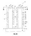
- FIGS. 2D and 3DAn etch-back, e.g., an anisotropic etch-back, is then performed to remove excess conductor to form control gates 265 from the remaining conductor, as shown in FIGS. 2D and 3D , where FIG. 2D is a cross-section (cross-hatching omitted) of memory array 200 taken along line 2 D- 2 D of FIG. 3D that is a cross-section (cross-hatching omitted) taken along line 3 D- 3 D of FIG. 2D .
- FIGS. 2D and 3Dwhere FIG. 2D is a cross-section (cross-hatching omitted) of memory array 200 taken along line 2 D- 2 D of FIG. 3D that is a cross-section (cross-hatching omitted) taken along line 3 D- 3 D of FIG. 2D .
- Control gates 265 1,1 and 265 1,2are respectively control gates of select gates, such as source select gates 270 1 and 270 2 ; control gates 265 2,1 and 265 2,2 are respectively control gates of memory cells (e.g., non-volatile memory cells) 272 1 and 272 2 ; and control gates 265 3,1 and 265 3,2 are respectively control gates of select gates, such as s drain select gates 274 1 and 274 2 , as shown in FIGS. 2D and 3D .
- Control gates 265 2,1 and 265 2,2may respectively form portions of access lines (e.g., word lines) 280 1 and 280 2 , as shown in FIG. 3D .
- control gates 265 2,1 and 265 2,2may be respectively coupled to word lines 280 1 and 280 2 .
- control gates 265 1,1 and 265 1,2respectively form portions of source select lines and control gates 265 3,1 and 265 3,2 respectively form portions of drain select lines.
- control gates 265 1,1 and 265 1,2may be respectively coupled to the source select lines, and control gates 265 3,1 and 265 3,2 may be respectively coupled to the drain select lines.
- a memory cell 272is located at each intersection of a word line 280 and charge trap 260 ; a source select gate 270 is located at each intersection of a source select line and charge trap 260 ; and drain select gate 274 located at each intersection of a drain select line and charge trap 260 .
- a word line 280 1is commonly coupled to the memory cells 272 1 respectively on different pillars 235
- a word line 280 2is commonly coupled to the memory cells 272 2 respectively on those different pillars 235 , as shown in FIG. 3D .
- a portion of charge trap 260 and a dielectric 208 thereunder and on a sidewall of semiconductor structure 255 1are interposed between successive control gates 265 2,1 of successive memory cells 272 1 of a string of memory cells 272 1 and thus electrically isolate successive control gates 265 1 of a string of memory cells 272 1 from each other, as shown in FIG. 2D .
- a portion of charge trap 260 and a dielectric 208 thereunder and on a sidewall of semiconductor structure 255 2are interposed between successive control gates 265 2,2 of successive memory cells 272 2 of a string of memory cells 272 2 and thus electrically isolate successive control gates 265 2 of a string of memory cells 272 2 from each other, as shown in FIG. 2D .
- a portion of charge trap 260 and a dielectric 208 adjacent thereto and adjacent to a sidewall of semiconductor structure 255 1are interposed between the control gate 265 1,1 of a source select gate 270 1 and the control gate 265 2,1 of a memory cell 272 1 at one end of the string of memory cells 272 1 , electrically isolating those control gates, and between the control gate 265 3,1 of a drain select gate 274 1 and the control gate 265 2,1 of the memory cell 272 1 at the opposite end of the string of memory cells 272 1 , electrically isolating those control gates, as shown in FIG. 2D .
- a portion of charge trap 260 and a dielectric 208 adjacent thereto and adjacent to a sidewall of semiconductor structure 255 2are interposed between the control gate 265 1,2 of a source select gate 270 2 and the control gate 265 2,2 of a memory cell 272 2 at one end of the string of memory cells 272 2 , electrically isolating those control gates, and between the control gate 265 3,2 of a drain select gate 274 2 and the control gate 265 2,2 of the memory cell 272 2 at the opposite end of the string of memory cells 272 2 , electrically isolating those control gates.
- portions of charge trap 260are interposed between the sidewalls of semiconductor structures 255 1 and 255 2 and the control gates 265 , electrically isolating the semiconductor structures 255 1 and 255 2 from control gates 265 , as shown in FIGS. 2D and 3D .
- a portion of the charge trap 260 , a dielectric 208 , and a portion of dielectric 204may be optionally removed, e.g., using a etch selective to the charge trap 260 , dielectric 208 , and dielectric 204 .
- Removal of the portion of the charge trap 260exposes a portion of the upper surface 232 of each of the pillars 235 , portions of the semiconductor 220 over each of the pillars 235 , the upper ends of semiconductor structures 255 , portions of the sidewalls of semiconductor structures 255 adjacent their upper ends, and an upper surface of each of the control gates 265 3,1 and 265 3,2 , as shown in FIG. 2D .
- the dielectric 208is also removed from the portions of the sidewalls of semiconductor structures 255 adjacent their upper ends. Removal of the portion of dielectric 204 exposes portions of an upper surface of semiconductor 202 .
- Source/drain regions 275may then be formed (e.g. implanted) in the exposed semiconductors 220 and the exposed portions of the sidewalls of semiconductor structures 255 adjacent their upper ends, as shown in FIG. 2D .
- Source/drain regions 277e.g., source lines
- Source/drain regions 275 and 277may be n-type when semiconductor 202 is p-type and p-type when semiconductor 202 is n-type.
- Source/drain regions 277are electrically coupled to source select gates 270 1 and 270 2 by semiconductor structures 255 .
- source/drain regionssuch as source/drain regions 277 may be implanted in semiconductor 202 through openings 212 ( FIG. 2A ), e.g., using hard mask 210 as a mask or using the mask over hard mask 210 in the event that the mask is not yet removed.
- a contiguous source/drain regione.g., a plane located under the openings 212 and dielectric 204 may replace source/drain regions 277 and may be implanted in semiconductor 202 before forming dielectric 204 .
- contiguous source/drain regionmay electrically coupled to source select gates 270 1 and 270 2 by semiconductor structures 255 .
- a dielectric(not shown), such as bulk insulation, may then be formed over the structure in FIG. 2D so that source/drain regions 275 and 277 are covered thereby. Openings may then be formed within the dielectric to expose source/drain regions 275 . Contacts (not shown) may then be formed within the openings, e.g., so that a contact is in contact with each source/drain region. 275 .
- the dielectricwould be a doped silicate glass.
- doped silicate glassesinclude BSG (borosilicate glass), PSG (phosphosilicate glass), and BPSG (borophosphosilicate glass).
- BSGborosilicate glass
- PSGphosphosilicate glass
- BPSGborophosphosilicate glass
- TEOStetraethylorthosilicate
- the contactsmay comprise, consist of, or consist essentially of a metal or metal-containing layer and may be aluminum, copper, a refractory metal, or a refractory metal silicide layer.
- the conductormay contain multiple metal-containing layers, e.g., a titanium nitride (TiN) barrier layer formed over (e.g., in direct physical contact with) a source/drain region 275 , a titanium (Ti) adhesion layer formed over the barrier layer, and a tungsten (W) layer formed over the adhesion layer.
- TiNtitanium nitride
- Wtungsten
- a conductor(not shown) that may be metal, such as aluminum, may then be formed over the dielectric formed over the structure of FIG. 2D .
- the conductoris patterned, etched, and processed, e.g., using standard processing, to produce individual data lines, such as bit lines, that are electrically connected to the contacts, and thus the source/drain regions 275 and drain select gates 274 1 and 274 2 .
- Semiconductor structures 255 1 and 255 2respectively form channel regions of memory cells 272 1 and 272 2 and respectively electrically couple memory cells 272 1 and 272 2 in series to form strings (e.g., NAND strings) of memory cells 272 1 and 272 2 .
- stringse.g., NAND strings
- a channel(s)can be formed in a semiconductor structure 255 1
- a channel(s)can be formed in a semiconductor structure 255 2 .
- Semiconductor structure 255 1electrically couples a string of memory cells 272 1 in series to a source select gate 270 1 at one end of that string and a drain select gate 274 1 in series to the opposite end of that string
- semiconductor structure 255 2electrically couples a string of memory cells 272 2 in series to a source select gate 270 2 at one end of that string and a drain select gate 274 1 in series to the opposite end of that string, as shown in FIG. 2D .
- a string of memory cells 272 1 and the source select gate 270 1 and the drain select gate 274 1 coupled to the ends thereofare located adjacent to the same portion of the sidewall (e.g., the same side) of a respective pillar 235
- a string of memory cells 272 2 and the source select gate 270 2 and the drain select gate 274 2 coupled to the ends thereofare located adjacent to the same opposite portion of the sidewall (e.g., the same opposite side) of a respective pillar 235 .
- word lines 280 1 coupled to memory cells 272 1are coupled to the same portion of the sidewall (e.g., the same side) of charge trap 260
- word lines 280 2 coupled to memory cells 272 2are coupled to the same opposite portion of the sidewall (e.g., the same opposite side) of charge trap 260 .
- a source select gate 270 1 and a drain select gate 274 1 and the string of memory cells 272 1 electrically coupled theretoare formed adjacent to a first portion of the substantially vertical (e.g., vertical) sidewall each pillar 235 .
- a source select gate 270 2 and a drain select gate 274 2 and the string of memory cells 272 2 electrically coupled theretoare formed adjacent to a second portion of the substantially vertical (e.g., vertical) sidewall the respective pillar 235 , as shown in FIGS. 2D and 3D . That is, there are two strings of memory cells on each pillar 235 .
- Each memory cell 272 1includes a portion of semiconductor structure 255 1 , as a channel region thereof, adjacent to (e.g., in direct contact with) an outer surface of the first portion of the sidewall of a respective pillar 235 , a portion of a charge trap 260 adjacent to the portion of semiconductor structure 255 1 , and a control gate 265 2,1 adjacent to the portion of charge trap 260 , as shown in FIGS. 2D and 3D .
- Each memory cell 272 2includes a portion of semiconductor structure 255 2 , as a channel region thereof adjacent to (e.g., in direct contact with) an outer surface of the second portion of the sidewall of the respective pillar 235 , an other portion of the charge trap 260 adjacent to the portion of the semiconductor structure 255 2 , and a control gate 265 2,2 adjacent to the other portion of the charge trap 260 , as shown in FIGS. 2D and 3D .
- the control gates 265 2,1 and 265 2,2 respectively of memory cells 272 1 and 272 2are formed adjacent to opposing portions of charge trap 260 , e.g., the portions that respectively wrap around opposing portions of the sidewall of each pillar 235 .
- two memory cellssuch as memory cells 272 1 and 272 2 , may respectively wrap around opposing portions of the sidewall of each pillar 235 , e.g., and as such, may be termed “half-wrap” memory cells.
- Control gates 265 2,1 and 265 2,2may be electrically isolated from each other, e.g., by a dielectric (not shown), e.g., bulk insulation, that may be formed between control gates 265 2,1 and 265 2,2 , and thus the word lines 280 1 and 280 2 .
- Adjacent word lines 280 2may be similarly electrically isolated from each other.
- charge trap 260may form a contiguous structure that is wrapped completely around the periphery of a respective pillar 235 , including the semiconductor structures 255 1 and 255 2 .
- the portions of charge trap 260 respectively adjacent to semiconductor structures 255 1 and 255 2may be contiguous.
- Portions of the charge trap 260may be interposed between a semiconductor structure 255 1 and a semiconductor structure 255 2 .
- the portions of charge trap 260 interposed between a semiconductor structure 255 1 and a semiconductor structure 255 2may be respectively in direct contact with opposing portions 230 of the sidewall of the respective pillar 235 , as shown in FIG. 3D .
- a portion of the charge traps 260 located between word lines 280 1 and 280 2may be removed, e.g., using an isotropic etch, after forming the individual word lines 280 1 and 280 2 . This separates a charge trap 260 into separated first and second portions respectively adjacent to semiconductor structures 255 1 and 255 2 .
- the separated first and second portions of the charge trap 260may wrap (e.g., completely) around the structures 255 1 and 255 2 , as indicated by dashed lines 291 in FIG. 3C , with the portion of charge trap 260 and dielectric pillar 235 between dashed lines 291 being omitted.
- Source select gates 270 1 and 270 2 and drain select gates 274 1 and 274 2have substantially the same (e.g., the same) cross-sections as those shown for memory cells 272 in FIG. 3D .
- a source select gate 270 1may include a portion of semiconductor structure 255 1 , as a channel region thereof, adjacent to the first portion of the sidewall of a respective pillar 235 , a portion of a charge trap 260 adjacent to the portion of semiconductor structure 255 1 , and a control gate 265 1,1 adjacent to the portion of charge trap 260 , as shown in FIG. 2D .
- a source select gate 270 2may include a portion of a semiconductor structure 255 2 , as a channel region thereof, adjacent to the second portion of the sidewall of a respective pillar 235 , a portion of a charge trap 260 adjacent to the portion of semiconductor structure 255 2 , and a control gate 265 1,2 adjacent to the portion of charge trap 260 , as shown in FIG. 2D .
- a drain select gate 274 1may include a other portion of semiconductor structure 255 1 , as a channel region thereof, adjacent to the first portion of the sidewall of a respective pillar 235 , an other portion of a charge trap 260 adjacent to the other portion of semiconductor structure 255 1 , and an other portion control gate 265 3,1 adjacent to the other portion of charge trap 260 , as shown in FIG. 2D .
- a drain select gate 274 2may include an other portion of semiconductor structure 255 2 , as a channel region thereof, adjacent to the second portion of the sidewall of a respective pillar 235 , an other portion of charge trap 260 adjacent to the other portion of semiconductor structure 255 2 , and a control gate 265 3,2 adjacent to the other portion of charge trap 260 , as shown in FIG. 2D .
- the source and drain select gatescan be programmable, i.e., capable of altering their threshold voltages, and may be programmed or left unprogrammed.
- FIGS. 4A-4E and 5 A- 5 Eare cross-sectional views of a portion of a memory array 400 , during various stages of fabrication, according to other embodiments.
- Memory array 400may form a portion of memory array 104 of FIG. 1 .
- Common numberingis used in FIGS. 4A-4E and 5 A- 5 E and in FIGS. 2A-2D and 3 A- 3 D to denote similar (e.g., the same) components.
- FIG. 4Ais a cross-section (cross-hatching omitted) of memory array 400 taken along line 4 A- 4 A of FIG. 5A that is a cross-section (cross-hatching omitted) taken along line 5 A- 5 A of FIG. 4A .
- the formation of the structure of FIGS. 4A and 5Amay be substantially the same as the formation of the structure of FIGS. 2A and 3A , as described above.
- Openings 412may be formed, e.g., as described above in conjunction with FIGS. 2A and 3A for openings 212 , except that the shape of the cross-sections of openings 412 in FIG. 5A differs from the shape of the cross-sections openings 212 in FIG. 3A .
- Semiconductor 214is formed in openings 412 so as to line or fill openings 412 , e.g., as described above in conjunction with FIGS. 2A and 3A for openings 212 , except that the shape of the cross-sections of semiconductor 214 in FIG. 5A differs from the shape of the cross-sections of semiconductor 214 in FIG. 3A .
- substantially vertical (e.g., vertical) dielectric pillar structures 435are formed within openings 212 from dielectric 216 , e.g., as described above in conjunction with FIGS. 2A and 3A for pillars 235 , except the shape of the cross-sections of pillar structures 435 in FIG. 5A differs from the shape of the cross-sections pillars 235 in FIG. 3A .
- FIG. 4Bis a cross-section (cross-hatching omitted) of memory array 400 taken along line 4 B- 4 B of FIG. 5B that is a cross-section (cross-hatching omitted) taken along line 5 B- 5 B of FIG. 4B .
- the formation of the structure of FIGS. 4B and 5Bmay be substantially the same as the formation of the structure of FIGS. 2B and 3B , as described above.
- a mask(not shown), e.g., of photoresist, may be formed over the structure of FIG.
- the exposed portions of hard mask 210 and the dielectrics 206 and 208are then removed, e.g., as described above in conjunction with FIGS. 2B and 3B .
- the exposed portion of semiconductor 220 ( FIG. 4B ) and portions of semiconductor 214e.g., portions of the substantially vertical (e.g., vertical) sidewalls of semiconductor 214 ( FIG. 5B ) are removed, e.g., as described above in conjunction with FIGS. 2B and 3B , stopping on or within dielectrics 204 and 216 .
- the removal of the portion of semiconductor 220stops on or within dielectric 216 and the removal of the portions of the substantially vertical sidewalls of semiconductor 214 stops on or within dielectric 204 .
- the etch that removes the portion of semiconductor 220 and the portions of semiconductor 214may have a different chemistry than and may be performed in situ with the etch that removes portions of hard mask 210 and the dielectrics 206 and 208 .
- portions of the substantially vertical (e.g., vertical) sidewalls of semiconductor 214exposes portions 430 of the substantially vertical (e.g., vertical) sidewalls of each pillar structure 435 , as shown in FIG. 5B
- removal of the portion of semiconductor 220exposes a portion of an upper surface 432 of each pillar structure 435 , as shown in FIGS. 4B and 5B
- portions of sacrificial dielectrics 206 , portions of dielectrics 204 and 208 , and portions of hard mask 210remain adjacent to (e.g., on) the sidewalls of semiconductor 214 , i.e., adjacent to the substantially vertical (e.g., vertical) sidewalls of semiconductor 214 .
- Removal of semiconductor 214 from the portions 430 of the substantially vertical (e.g., vertical) sidewalls of each pillar structure 435forms two separated opposing, substantially vertical (e.g., vertical) adjacent semiconductor structures 414 1 and 414 2 adjacent to (e.g., on) the remainder of the substantially vertical (e.g., vertical) sidewalls of each pillar structure 435 from semiconductor 214 , as shown in FIGS. 4B and 5B .
- opposing portions 430 of the sidewall of a pillar structure 435are interposed between and separate semiconductor structures 414 1 and 414 2 from each other.
- portions of semiconductor 220 that are separated by the removal of the portion thereofare respectively electrically coupled (e.g. by direct physical contact with) to semiconductor structures 414 1 and 414 2 , as shown in FIGS. 4B and 5B .
- FIGS. 4B and 5Bmay then be patterned to form the structure of FIGS. 4C and 5C , where FIG. 4C is a cross-section (cross-hatching omitted) of memory array 400 taken along line 4 C- 4 C of FIG. 5C that is a cross-section (cross-hatching omitted) taken along line 5 C- 5 C of FIG. 4C .
- a mask(not shown), e.g., of photoresist, may formed over the structure of FIGS.
- openings 440are formed through dielectric 216 and extends through semiconductor structures 414 1 and 414 2 , as shown in FIG. 5C .
- a portion each semiconductor 220 over a pillar structure 435 and a portion of each of semiconductor structures 414 1 and 414 2 that extends above the upper surface 432 of each pillar structure 435 patterned for removalare then removed, such as by etching (e.g., using an etch that is selective to polysilicon), stopping on or within a respective pillar structure 435 , thereby forming an upper portion of a respective opening 440 .
- etchinge.g., using an etch that is selective to polysilicon
- each of semiconductor structures 414 1 and 414 2 patterned for removal and a portion of each pillaris removed, such as by etching (e.g., using an etch chemistry different than that used for forming upper portion of a respective opening 440 ), stopping on or within semiconductor 202 , thereby forming the remainder of each opening 440 .
- each opening 440forms two separate pillars 445 1 and 445 2 from each pillar structure 435 , as shown in FIG. 5C .
- the formation of each opening 440also forms a semiconductor structure 455 1 and a semiconductor structure 455 2 from each semiconductor structure 414 1 that are separated from each other and a semiconductor structure 455 1 and a semiconductor structure 455 2 from each semiconductor structure 414 2 that are separated from each other.
- Semiconductor structures 455 1are respectively adjacent to (e.g., on) opposing portions of the sidewall (e.g., opposite corners) of each pillar 445 1 and are separated from each other, as shown in FIG. 5C .
- Semiconductor structures 455 2are respectively adjacent to (e.g., on) opposing portions (e.g., opposite corners) of the sidewall each pillar 445 2 and are separated from each other, as further shown in FIG. 5C . This means that there are semiconductor structures 455 1 respectively on opposite corners of each of pillars 445 1 , and there are semiconductor structures 455 2 respectively on opposite corners of each of pillars 445 2 .
- each semiconductor structure 455may be respectively intersected by planes that are substantially perpendicular (e.g., perpendicular) to each other, as shown in FIG. 5C , e.g., the ends may be about 90 degrees apart.
- the portion of semiconductor 220 that is coupled to semiconductor structure 414 1is cut into two parts during the formation of opening 440 so that the two parts are respectively electrically coupled to (e.g., by direct physical contact with) a set of semiconductor structures 455 1 and 455 2 .
- the portion of semiconductor 220 that is coupled to semiconductor structure 414 2is also cut into two parts during the formation of opening 440 so that the two parts are respectively electrically coupled to (e.g., by direct physical contact with) a set of semiconductor structures 455 1 and 455 2 .
- Each pillar 445 1has a substantially vertical (e.g., vertical) sidewall 443 1
- each pillar 445 2has a substantially vertical (e.g., vertical) sidewall 443 2 , as shown in FIGS. 4C and 5C
- Each sidewall 443 1has an exposed substantially vertical (e.g., vertical) portion 442 1 and an exposed substantially vertical (e.g., vertical) portion 447 1 that is the same as an exposed portion 430 of the single pillar structure 435 .
- Remaining portions of each sidewall 443 1e.g., other than portions 442 1 and 447 1 , are covered by semiconductor structures 455 1 .
- Each sidewall 443 2has an exposed substantially vertical (e.g., vertical) portion 442 2 and an exposed substantially vertical (e.g., vertical) portion 447 2 that is the same as another exposed portion 430 of the single pillar structure 435 .
- Remaining portions of each sidewall 443 2e.g., other than portions 442 2 and 447 2 , are covered by semiconductor structures 455 2 . Note that the exposed portions 442 and 447 may face in opposite directions.
- the cross-section taken along line 4 B- 4 B in FIG. 5C and shown in FIG. 4Bis substantially unaffected (e.g., unaffected) by the formation of openings 440 . That is, the cross-section taken along line 4 B- 4 B in FIG. 5B before the formation of openings 440 and the cross-section taken along line 4 B- 4 B in FIG. 5C after the formation of openings 440 remains substantially the same (e.g., the same), as is apparent from using FIG. 4B to correspond to both the cross-sections taken along lines 4 B- 4 B in FIGS. 5B and 5C .
- FIG. 4Dis a cross-section (cross-hatching omitted) of memory array 400 taken along line 4 D- 4 D of FIG. 5D that is a cross-section (cross-hatching omitted) taken along line 5 D- 5 D of FIG. 4D .
- the formation of the structure of FIGS. 4D and 5Dmay be substantially the same as the formation of the structure of FIGS. 2C and 3C , as described above.
- sacrificial dielectrics 206are then removed from dielectrics 204 and 208 and semiconductor structures 455 1 and 455 2
- sacrificial hard mask 210is removed from a dielectric 208 , e.g., as described above in conjunction with FIGS. 2C and 3C .
- a plurality of charge storage structuresis formed substantially concurrently (e.g., concurrently) adjacent to the dielectrics 204 and 208 , semiconductor structures 455 1 and 455 2 , and portions 442 and 447 of the substantially vertical (e.g., vertical) sidewalls 443 of each pillar 445 , as shown in FIGS. 4D and 5D , e.g., as described above in conjunction with FIGS. 2C and 3C .
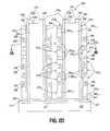
- FIG. 4Eis a cross-section (cross-hatching omitted) of memory array 400 taken along line 4 E- 4 E of FIG. 5E that is a cross-section (cross-hatching omitted) taken along line 5 E- 5 E of FIG. 4E .
- the formation of the structure of FIGS. 4E and 5Emay be substantially the same as the formation of the structure of FIGS. 2D and 3D , as described above.
- control gates 465are formed from a conductor, e.g., as described above in conjunction with FIGS. 2D and 3D for control gates 265 .
- control gates 465 1,1 and 465 1,2are respectively control gates of select gates, such as source select gates 470 2,1 and 470 2,2 ; control gates 465 2,1 and 465 2,2 are respectively control gates of memory cells (e.g., non-volatile memory cells) 472 2,1 and 472 2,2 ; and control gates 465 3,1 and 465 3,2 are respectively control gates of select gates, such as drain select gates 474 2,1 and 474 2,2 , as shown in FIGS. 4E and 5E .
- Control gates 465 2,1 and 465 2,2may respectively form portions of access lines (e.g., word lines 480 1 and 480 2 ) as shown in FIG. 5E .
- control gates 465 2,1 and 465 2,2may be respectively coupled to word lines 480 1 and 480 2 .
- control gates 465 1,1 and 465 1,2respectively form portions of source select lines and control gates 465 3,1 and 465 3,2 respectively form portions of drain select lines.
- control gates 465 1,1 and 465 1,2may be respectively coupled to the source select lines and control gates 465 3,1 and 465 3,2 may be respectively coupled to the drain select lines.
- a memory cell 472is located at each intersection of a word line 480 and charge trap 260 ;
- a source select gate 470is located at each intersection of a source select line and charge trap 260 ;
- drain select gate 474located at each intersection of a drain select line and charge trap 260 .
- control gates 465After forming control gates 465 , a portion of the charge trap 260 , a dielectric 208 , and a portion of dielectric 204 may be optionally removed, e.g., as described above in conjunction with FIGS. 2D and 3D , exposing a portion of an upper surface of each of the pillar structures 435 , portions of the semiconductor 220 adjacent to each of the pillars 235 , the upper ends of semiconductor structures 455 , portions of the sidewalls of semiconductor structures 455 adjacent their upper ends, and an upper surface of each of the control gates 465 3,1 and 465 3,2 , as shown in FIG. 4E .
- Source/drain regions 275may then be formed (e.g. implanted) in the exposed semiconductors 220 and the exposed portions of the sidewalls of semiconductor structures 455 adjacent their upper ends, as shown in FIG. 4E , e.g., as described above in conjunction with FIG. 2D .
- Source/drain regions 277e.g., source lines
- Source/drain regions 277may be formed (e.g. implanted), e.g. substantially concurrently (e.g., concurrently) with source/drain regions 275 in the exposed portions of semiconductor 202 , e.g., as described above in conjunction with FIG. 2D .
- Data linesmay be electrically coupled to source/drain regions 275 , and thus the drain select gates 474 2,1 and 274 2,2 , by contacts, e.g., as described above in conjunction with FIG. 2D .
- Source/drain regions 277are electrically coupled to source select gates 470 2,1 and 470 2,2 by semiconductor structures 455 2 .
- the two semiconductor structures 455 2 formed adjacent to (e.g. on) each of pillars 445 2respectively form channel regions of memory cells 472 2,1 and 472 2,2 and electrically couple memory cells 472 2,1 and 472 2,2 in series to form strings (e.g., NAND strings) of memory cells 472 2,1 and 472 2,2 .
- stringse.g., NAND strings
- a channel(s)can be formed in the respective semiconductor structure 455 2
- a channel(s)can be formed in the respective semiconductor structure 455 2 .
- One of the semiconductor structures 455 2electrically couples a string of memory cells 472 2,1 in series to a source select gate 470 2,1 at one end of that string and a drain select gate 474 2,1 in series to the opposite end of that string
- the other semiconductor structure 455 2electrically couples a string of memory cells 472 2,2 in series to a source select gate 470 2,2 at one end of that string and a drain select gate 474 2,2 in series to the opposite end of that string, as shown in FIG. 4E .
- a source select gate 470 2,1 , a drain select gate 474 2,1 , and the string of memory cells 472 2,1 electrically coupled theretoare formed adjacent to a first portion of the substantially vertical (e.g., vertical) sidewall each pillar 445 2
- a source select gate 470 2,2 , a drain select gate 474 2,2 , and the string of memory cells 472 2,2 electrically coupled theretoare formed adjacent to a second portion of the substantially vertical (e.g., vertical) sidewall the respective pillar 445 2 , as shown in FIGS. 4E and 5E . That is, there are two strings of memory cells with source and drain select gates coupled thereto adjacent to (e.g., on) each pillar 445 2 .
- each pillar 445 1There are two strings of memory cells with source and drain select gates coupled thereto adjacent to (e.g., on) each pillar 445 1 .
- the two semiconductor structures 455 1 formed adjacent to (e.g., on) each of pillars 445 1respectively form channel regions of memory cells 472 1,1 and 472 1,2 ( FIG. 5E ) and electrically couple memory cells 472 1,1 and 472 1,2 in series to form strings (e.g., NAND strings) of memory cells 472 1,1 and 472 1,2 .
- the ends of each of these stringsare respectively coupled to a source select gate and a drain select gate by a respective one of the two semiconductor structures 455 1 .
- a string of memory cells 472 1,1(e.g., NAND string) coupled in series and the source and a drain select gates respectively coupled in series to the ends thereof are located adjacent to a first portion of the sidewall of a respective pillar 445 1
- a string of memory cells 472 1,2(e.g., NAND string) coupled in series and the source and a drain select gates respectively coupled in series to the ends thereof are located adjacent to a second portion of the sidewall of the respective pillar 445 1 .
- Each memory cell 472 1,1includes a portion of semiconductor structure 455 1 , as a channel region thereof, adjacent to (e.g., in direct contact with) an outer surface of a first portion (e.g., a corner) of the sidewall 443 1 ( FIG. 5D ) of a respective pillar 445 1 , a portion of a charge trap 260 adjacent to the portion of semiconductor structure 455 1 , and a control gate 465 2,1 adjacent to the portion of charge trap 260 , as shown in FIG. 5E .
- Each memory cell 472 1,2includes a portion of an other semiconductor structure 455 1 , as a channel region thereof, adjacent to (e.g., in direct contact with) an outer surface of a second portion (e.g., an opposite corner) of the sidewall 443 1 of the respective pillar 445 1 , an other portion of the charge trap 260 adjacent to the portion of the other semiconductor structure 455 1 , and a control gate 465 2,2 adjacent to the other portion of the charge trap 260 , as shown in FIG. 5E .
- a memory cell 472 1,1 and a memory cell 472 1,2may wrap around portions of sidewall 443 1 of a pillar 445 1 .
- Each memory cell 472 2,1includes a portion of semiconductor structure 455 2 , as a channel region thereof, adjacent to (e.g., in direct contact with) an outer surface of a first portion (e.g., a corner) of the sidewall 443 2 ( FIG. 5D ) of a respective pillar 445 2 , a portion of a charge trap 260 adjacent to the semiconductor structure 455 2 , and a control gate 465 2,1 adjacent to the portion of the charge trap 260 , as shown in FIGS. 4E and 5E .
- Each memory cell 472 2,2includes a portion of an other semiconductor structure 455 2 , as a channel region thereof, adjacent to (e.g., in direct contact with) an outer surface of a second portion (e.g., an opposite corner) of the sidewall 443 2 of the respective pillar 445 2 , an other portion of the charge trap 260 adjacent to the portion of the other semiconductor structure 455 2 , and a control gate 465 2,2 adjacent to the other portion of the charge trap 260 , as shown in FIGS. 4E and 5E .
- a memory cell 472 2,1 and a memory cell 472 2,2may wrap around portions of sidewall 443 2 of a pillar 445 2 .
- memory cells 472 1,1 , 472 1,2 , 472 2,1 , and 472 2,1respectively wrap around the four corners of a pillar structure 435 , e.g., and as such, may be termed “quarter-wrap” memory cells.
- Control gates 465 2,1 and 465 2,2may be electrically isolated from each other, e.g., by a dielectric (not shown), e.g., bulk insulation, that may be formed between word lines 480 1 and 480 2 .
- Adjacent word lines 480 2may be similarly isolated from each other.
- charge traps 260may form contiguous structures that are wrapped completely around the peripheries of pillars 445 1 , including the two semiconductor structures 455 1 adjacent thereto, and completely around the peripheries of pillars 445 2 , including the two semiconductor structures 455 2 adjacent thereto.
- a portion of a charge trap 260may be interposed between the two semiconductor structures 455 2 on the sidewall 443 2
- a portion of a charge trap 260may be interposed between the two semiconductor structures 455 1 on the sidewall 443 1 .
- a dielectrice.g., bulk insulation, may be formed in an opening 485 , i.e., remaining portion of an opening 440 ( FIG. 5C ), located between portions of the charge traps 260 wrapped around the peripheries of pillars 445 1 and 445 2 .
- Portions 442 1 and 442 2 respectively of sidewalls 443 1 and 443 2 respectively of pillars 445 1 and 445 2may face each other, as shown in FIG. 5E . Note that portions 442 1 and 442 2 are covered by portions of charge trap 260 , but are devoid of conductor, such as portions of semiconductor structures 455 .
- Source select gates 470 and drain select gates 474have substantially the same (e.g., the same) cross-sections as those shown for memory cells 472 in FIG. 5E .
- Each source select gate 470 2,1includes a portion of semiconductor structure 455 2 , as a channel region thereof, adjacent to (e.g., in direct contact with) the outer surface of the first portion (e.g., the corner) of the sidewall of a respective pillar 445 2 , a portion of a charge trap 260 adjacent to the portion of semiconductor structure 455 2 , and a control gate 465 1,1 adjacent to the portion of charge trap 260 , as shown in FIG. 4E .
- Each source select gate 470 2,2includes a portion of the other semiconductor structure 455 2 , as a channel region thereof, adjacent to (e.g., in direct contact with) the outer surface of the second portion (e.g., the opposite corner) of the sidewall of the respective pillar 445 2 , an other portion of the charge trap 260 adjacent to the portion of the other semiconductor structure 455 2 , and a control gate 465 1,2 adjacent to the other portion of the charge trap 260 , as shown in FIG. 4E .
- a source select gate 470 2,1 and a source select gate 470 2,2may wrap around portions of the sidewall of a pillar 445 2 in a manner similar to that shown in FIG. 5E for memory cells 472 2,1 and 472 2,2 .
- four source select gatesrespectively wrap around the four corners of a pillar structure 435 , e.g., and as such, may be termed “quarter-wrap” source select gates.
- Each drain select gate 474 2,1includes a portion of semiconductor structure 455 2 , as a channel region thereof, adjacent to (e.g., in direct contact with) the outer surface of the first portion (e.g., the corner) of the sidewall of a respective pillar 445 2 , a portion of a charge trap 260 adjacent to the portion of semiconductor structure 455 2 , and a control gate 465 3,1 adjacent to the portion of charge trap 260 , as shown in FIG. 4E .
- Each drain select gate 474 2,2includes a portion of the other semiconductor structure 455 2 , as a channel region thereof, adjacent to (e.g., in direct contact with) the outer surface of the second portion (e.g., the opposite corner) of the sidewall of the respective pillar 445 2 , an other portion of the charge trap 260 adjacent to the portion of the other semiconductor structure 455 2 , and a control gate 465 3,2 adjacent to the other portion of the charge trap 260 , as shown in FIG. 4E .
- a drain select gate 474 2,1 and a drain select gate 474 2,2may wrap around portions of the sidewall of a pillar 445 2 in a manner similar to that shown in FIG. 5E for memory cells 472 2,1 and 472 2,2 .
- drain select gatesrespectively wrap around the four corners of a pillar structure 435 , e.g., and as such may be termed quarter-wrap drain select gates.
- the source and drain select gatescan be programmable and may be programmed or left unprogrammed.
- a word line 480 1is commonly coupled to the memory cells 472 1,1 and 472 2,1 respectively on different pillars 445 1 and 445 2
- a word line 480 2is commonly coupled to the memory cells 472 1,2 and 472 2,2 respectively on those different pillars 445 1 and 445 2 , as shown in FIG. 5E .
- the access-line (e.g., word-line) pitch WL Pitch200 and the data-line (e.g., bit-line) pitch BL Pitch200are shown for memory array 200 .
- the bit-line pitchmay be the pitch of the memory cells commonly coupled to a word line, e.g., in the word-line direction, while the word-line pitch may be the pitch of the memory cells in the bit-line direction.
- the thickness of a semiconductor structure 255e.g., the term Tsi
- the term Tsioccurs twice in the pitch BL Pitch200 .
- the access-line (e.g., word-line) pitch WL Pitch400 and the data-line (e.g., bit-line) pitch BP Pitch400are shown for memory array 400 .
- the distance PSmay be substantially the same (e.g., the same as) WS.
- the thickness of a semiconductor structure 455e.g., the term Tsi
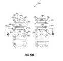
- FIG. 6is a cross-sectional view (cross-hatching omitted) of a memory array 600 , as viewed from the top, according to the prior art.
- FIG. 6is analogous to the views of FIGS. 3D and 5E .
- Memory array 600includes a plurality of memory cells 672 that are coupled to access lines, e.g., word lines 680 .
- Each memory cell 672is completely wrapped around a sidewall (e.g., the perimeter) of a pillar 635 that may be formed from a dielectric.
- a memory cell 672may be termed a “full-wrap” memory cell, as compared with the “half-wrap” memory cells 272 of memory array 200 in FIG. 3D and the “quarter-wrap” memory cells 472 of memory array 400 in FIG. 5E .
- a string of series coupled memory cells 672is formed adjacent to each pillar 635 , i.e., one string per pillar 635 .
- Each memory cell 672includes a semiconductor 614 formed adjacent to and completely wrapped around a respective pillar 635 .
- a charge trap 660is formed adjacent to and is completely wrapped around a respective semiconductor 614 .
- a control gate 665 that forms a portion of a respective word line 680is formed adjacent to and is completely wrapped around a respective charge trap 660 .
- the access-line (e.g., word-line) pitch WL PitchPA and the data-line (e.g., bit-line) pitch BL PitchPAare shown for memory array 600 in FIG. 6 .
- ⁇ WL Pitch60 nm. That is, the word-line pitch for the “half-” and “quarter-wrap” memory cells is expected to be about 38 percent less than the word line pitch for the “full-wrap” memory cells of the prior art, based on the typical values.
- equation (8)still typically gives a number greater than zero.
- Tsi10 nm
- OD30 nm
- PS30 nm
- R10 nm
- W10 nm
- ⁇ BL Pitch(PA-400)30 nm. That is, the bit-line pitch for the “quarter-wrap” memory cells is expected to be about 30 percent less than the bit-line pitch for the “full-wrap” memory cells of the prior art, based on the typical values.
- bit-line pitch of the “full-wrap” memory cells of the prior art and the bit-line pitch for the “half-wrap” cellsare the same, the bit-line pitch for the “quarter-wrap” memory cells is expected to be about 30 percent less than the bit-line pitch for the “half-wrap” memory cells.
- thisis due, at least in part, to the fact that adjacent quarter-wrap” memory cells in the word line direction and commonly coupled to a single word line 480 are located adjacent to pillars 445 1 and 445 2 ( FIG. 5E ) that are formed from a single dielectric pillar structure 435 ( FIG.
- adjacent half-wrap” memory cells in the word line direction and commonly coupled to a single word line 280are located adjacent to separate pillars 235 ( FIG. 3D ) that are formed from separate dielectrics formed in separate openings.
Landscapes
- Semiconductor Memories (AREA)
- Non-Volatile Memory (AREA)
- Dram (AREA)
Abstract
Description
WLPitch200=WS+2(R+W)+CTF+Tsi (1)
and the bit-line pitch BLPitch200may be expressed as
BLPitch200=W+2Tsi+2CTF+OD (2)
where the distances WS, (R+W), CTF, W, and Tsi are shown in
WLPitch400=WS+2(R+W)+CTF+Tsi (3)
and the bit-line pitch BLPitch400may be expressed as
BLPitch400=0.5PS+0.5W+(R+W)+Tsi+CTF (4)
where the distances WS, (R+W), CTF, PS, W, and Tsi are shown in
WLPitchPA=WS+2(R+W)+2CTF+2Tsi+OD (5)
and the bit-line pitch BLPitchPAmay be expressed as
BLPitchPA=W+2CTF+2Tsi+OD (6)
where the distances WS, (R+W), CTF, OD, W, and Tsi are shown in
ΔWLpitch=CTF+Tsi+OD (7)
which is clearly greater than zero.
ΔBLPitch(PA-400)=CTF+Tsi+OD−0.5PS−R−0.5W (8)
Claims (39)
Priority Applications (10)
| Application Number | Priority Date | Filing Date | Title |
|---|---|---|---|
| US12/836,853US8237213B2 (en) | 2010-07-15 | 2010-07-15 | Memory arrays having substantially vertical, adjacent semiconductor structures and the formation thereof |
| KR1020137003357AKR101395526B1 (en) | 2010-07-15 | 2011-06-13 | Memory arrays having substantially vertical, adjacent semiconductor structures and their formation |
| PCT/US2011/040122WO2012009076A2 (en) | 2010-07-15 | 2011-06-13 | Memory arrays having substantially vertical, adjacent semiconductor structures and their formation |
| EP11807222.2AEP2593966B1 (en) | 2010-07-15 | 2011-06-13 | Memory arrays having substantially vertical, adjacent semiconductor structures and their formation |
| CN201180034861.6ACN102986028B (en) | 2010-07-15 | 2011-06-13 | Memory array with substantially vertical adjacent semiconductor structures and formation thereof |
| JP2013519688AJP5578460B2 (en) | 2010-07-15 | 2011-06-13 | Memory arrays having substantially vertical adjacent semiconductor structures and their formation |
| TW100123685ATWI485712B (en) | 2010-07-15 | 2011-07-05 | Memory array having substantially vertical, adjacent semiconductor structures and forms thereof |
| US13/547,399US8564045B2 (en) | 2010-07-15 | 2012-07-12 | Memory arrays having substantially vertical, adjacent semiconductor structures and the formation thereof |
| US14/028,987US9147681B2 (en) | 2010-07-15 | 2013-09-17 | Electronic systems having substantially vertical semiconductor structures |
| JP2014037681AJP5785286B2 (en) | 2010-07-15 | 2014-02-28 | Memory arrays having substantially vertical semiconductor structures adjacent to each other and their formation |
Applications Claiming Priority (1)
| Application Number | Priority Date | Filing Date | Title |
|---|---|---|---|
| US12/836,853US8237213B2 (en) | 2010-07-15 | 2010-07-15 | Memory arrays having substantially vertical, adjacent semiconductor structures and the formation thereof |
Related Child Applications (1)
| Application Number | Title | Priority Date | Filing Date |
|---|---|---|---|
| US13/547,399ContinuationUS8564045B2 (en) | 2010-07-15 | 2012-07-12 | Memory arrays having substantially vertical, adjacent semiconductor structures and the formation thereof |
Publications (2)
| Publication Number | Publication Date |
|---|---|
| US20120012921A1 US20120012921A1 (en) | 2012-01-19 |
| US8237213B2true US8237213B2 (en) | 2012-08-07 |
Family
ID=45466270
Family Applications (3)
| Application Number | Title | Priority Date | Filing Date |
|---|---|---|---|
| US12/836,853Active2031-02-01US8237213B2 (en) | 2010-07-15 | 2010-07-15 | Memory arrays having substantially vertical, adjacent semiconductor structures and the formation thereof |
| US13/547,399ActiveUS8564045B2 (en) | 2010-07-15 | 2012-07-12 | Memory arrays having substantially vertical, adjacent semiconductor structures and the formation thereof |
| US14/028,987Active2030-07-18US9147681B2 (en) | 2010-07-15 | 2013-09-17 | Electronic systems having substantially vertical semiconductor structures |
Family Applications After (2)
| Application Number | Title | Priority Date | Filing Date |
|---|---|---|---|
| US13/547,399ActiveUS8564045B2 (en) | 2010-07-15 | 2012-07-12 | Memory arrays having substantially vertical, adjacent semiconductor structures and the formation thereof |
| US14/028,987Active2030-07-18US9147681B2 (en) | 2010-07-15 | 2013-09-17 | Electronic systems having substantially vertical semiconductor structures |
Country Status (7)
| Country | Link |
|---|---|
| US (3) | US8237213B2 (en) |
| EP (1) | EP2593966B1 (en) |
| JP (2) | JP5578460B2 (en) |
| KR (1) | KR101395526B1 (en) |
| CN (1) | CN102986028B (en) |
| TW (1) | TWI485712B (en) |
| WO (1) | WO2012009076A2 (en) |
Cited By (55)
| Publication number | Priority date | Publication date | Assignee | Title |
|---|---|---|---|---|
| US20130044549A1 (en)* | 2011-08-15 | 2013-02-21 | Akira Goda | Apparatus and methods including source gates |
| US20130121081A1 (en)* | 2009-07-06 | 2013-05-16 | Kabushiki Kaisha Toshiba | Nonvolatile semiconductor memory device |
| US8461000B2 (en)* | 2010-06-30 | 2013-06-11 | Sandisk Technologies Inc. | Method of making ultrahigh density vertical NAND memory device |
| US20140021530A1 (en)* | 2010-07-15 | 2014-01-23 | Micron Technology, Inc. | Electronic systems having substantially vertical semiconductor structures |
| US8722525B2 (en) | 2011-06-21 | 2014-05-13 | Micron Technology, Inc. | Multi-tiered semiconductor devices and associated methods |
| US8759895B2 (en) | 2011-02-25 | 2014-06-24 | Micron Technology, Inc. | Semiconductor charge storage apparatus and methods |
| US8778762B2 (en) | 2012-12-07 | 2014-07-15 | Micron Technology, Inc. | Methods of forming vertically-stacked structures, and methods of forming vertically-stacked memory cells |
| US8853769B2 (en) | 2013-01-10 | 2014-10-07 | Micron Technology, Inc. | Transistors and semiconductor constructions |
| US8860937B1 (en) | 2012-10-24 | 2014-10-14 | Kla-Tencor Corp. | Metrology systems and methods for high aspect ratio and large lateral dimension structures |
| US8912495B2 (en) | 2012-11-21 | 2014-12-16 | Kla-Tencor Corp. | Multi-spectral defect inspection for 3D wafers |
| US8928061B2 (en) | 2010-06-30 | 2015-01-06 | SanDisk Technologies, Inc. | Three dimensional NAND device with silicide containing floating gates |
| US8987801B2 (en)* | 2011-12-13 | 2015-03-24 | Micron Technology, Inc. | Memory cells having a plurality of control gates and memory cells having a control gate and a shield |
| US20150115345A1 (en)* | 2013-10-25 | 2015-04-30 | Etienne Nowak | Vertical memory devices and methods of manufacturing the same |
| US9105737B2 (en) | 2013-01-07 | 2015-08-11 | Micron Technology, Inc. | Semiconductor constructions |
| US9136278B2 (en) | 2013-11-18 | 2015-09-15 | Micron Technology, Inc. | Methods of forming vertically-stacked memory cells |
| US9159845B2 (en) | 2013-05-15 | 2015-10-13 | Micron Technology, Inc. | Charge-retaining transistor, array of memory cells, and methods of forming a charge-retaining transistor |
| US9159739B2 (en) | 2010-06-30 | 2015-10-13 | Sandisk Technologies Inc. | Floating gate ultrahigh density vertical NAND flash memory |
| US9178077B2 (en) | 2012-11-13 | 2015-11-03 | Micron Technology, Inc. | Semiconductor constructions |
| US20160056302A1 (en)* | 2011-12-22 | 2016-02-25 | SK Hynix Inc. | Three-dimensional semiconductor device |
| US20160071871A1 (en)* | 2014-09-10 | 2016-03-10 | Kabushiki Kaisha Toshiba | Semiconductor memory device and method for manufacturing same |
| US9318199B2 (en) | 2012-10-26 | 2016-04-19 | Micron Technology, Inc. | Partial page memory operations |
| US9484196B2 (en) | 2014-02-25 | 2016-11-01 | Micron Technology, Inc. | Semiconductor structures including liners comprising alucone and related methods |
| US9524779B2 (en) | 2014-06-24 | 2016-12-20 | Sandisk Technologies Llc | Three dimensional vertical NAND device with floating gates |
| US9553146B2 (en) | 2014-06-05 | 2017-01-24 | Sandisk Technologies Llc | Three dimensional NAND device having a wavy charge storage layer |
| US9576966B1 (en) | 2015-09-21 | 2017-02-21 | Sandisk Technologies Llc | Cobalt-containing conductive layers for control gate electrodes in a memory structure |
| US9620515B2 (en) | 2015-05-13 | 2017-04-11 | Kabushiki Kaisha Toshiba | Semiconductor memory device |
| US9646975B2 (en) | 2015-09-21 | 2017-05-09 | Sandisk Technologies Llc | Lateral stack of cobalt and a cobalt-semiconductor alloy for control gate electrodes in a memory structure |
| US9780182B2 (en) | 2015-02-04 | 2017-10-03 | Sandisk Technologies Llc | Molybdenum-containing conductive layers for control gate electrodes in a memory structure |
| US9806089B2 (en) | 2015-09-21 | 2017-10-31 | Sandisk Technologies Llc | Method of making self-assembling floating gate electrodes for a three-dimensional memory device |
| US9984963B2 (en) | 2015-02-04 | 2018-05-29 | Sandisk Technologies Llc | Cobalt-containing conductive layers for control gate electrodes in a memory structure |
| US10128261B2 (en) | 2010-06-30 | 2018-11-13 | Sandisk Technologies Llc | Cobalt-containing conductive layers for control gate electrodes in a memory structure |
| US10249819B2 (en) | 2014-04-03 | 2019-04-02 | Micron Technology, Inc. | Methods of forming semiconductor structures including multi-portion liners |
| US10276583B2 (en) | 2015-10-29 | 2019-04-30 | Sandisk Technologies Llc | Three-dimensional memory device containing composite word lines including a metal silicide and an elemental metal and method of making thereof |
| US10510769B2 (en) | 2010-06-28 | 2019-12-17 | Micron Technology, Inc. | Three dimensional memory and methods of forming the same |
| US10541029B2 (en) | 2012-08-01 | 2020-01-21 | Micron Technology, Inc. | Partial block memory operations |
| US10622368B2 (en) | 2015-06-24 | 2020-04-14 | Sandisk Technologies Llc | Three-dimensional memory device with semicircular metal-semiconductor alloy floating gate electrodes and methods of making thereof |
| US10741572B2 (en) | 2015-02-04 | 2020-08-11 | Sandisk Technologies Llc | Three-dimensional memory device having multilayer word lines containing selectively grown cobalt or ruthenium and method of making the same |
| US10756109B2 (en) | 2018-09-06 | 2020-08-25 | Toshiba Memory Corporation | Semiconductor device |
| US10840259B2 (en) | 2018-08-13 | 2020-11-17 | Sandisk Technologies Llc | Three-dimensional memory device including liner free molybdenum word lines and methods of making the same |
| US20210175250A1 (en)* | 2017-04-24 | 2021-06-10 | Micron Technology, Inc. | Elevationally-Extending String of Memory Cells and Methods of Forming an Elevationally-Extending String of Memory Cells |
| US11223014B2 (en) | 2014-02-25 | 2022-01-11 | Micron Technology, Inc. | Semiconductor structures including liners comprising alucone and related methods |
| US11289506B2 (en)* | 2011-06-22 | 2022-03-29 | Kioxia Corporation | Semiconductor memory device and method for manufacturing same |
| US11330164B2 (en) | 2020-03-17 | 2022-05-10 | KLA Corp. | Determining focus settings for specimen scans |
| US11430805B2 (en)* | 2011-06-17 | 2022-08-30 | Kioxia Corporation | Semiconductor memory device including three-dimensional memory cell arrays |
| US11508445B2 (en) | 2015-09-30 | 2022-11-22 | Sunrise Memory Corporation | Capacitive-coupled non-volatile thin-film transistor strings in three dimensional arrays |
| US11644756B2 (en) | 2020-08-07 | 2023-05-09 | KLA Corp. | 3D structure inspection or metrology using deep learning |
| US11729980B2 (en) | 2017-06-20 | 2023-08-15 | Sunrise Memory Corporation | 3-dimensional NOR memory array architecture and methods for fabrication thereof |
| US11749495B2 (en) | 2021-10-05 | 2023-09-05 | KLA Corp. | Bandpass charged particle energy filtering detector for charged particle tools |
| US11839086B2 (en) | 2021-07-16 | 2023-12-05 | Sunrise Memory Corporation | 3-dimensional memory string array of thin-film ferroelectric transistors |
| US11842777B2 (en) | 2020-11-17 | 2023-12-12 | Sunrise Memory Corporation | Methods for reducing disturb errors by refreshing data alongside programming or erase operations |
| US11844204B2 (en) | 2019-12-19 | 2023-12-12 | Sunrise Memory Corporation | Process for preparing a channel region of a thin-film transistor in a 3-dimensional thin-film transistor array |
| US11915768B2 (en) | 2015-09-30 | 2024-02-27 | Sunrise Memory Corporation | Memory circuit, system and method for rapid retrieval of data sets |
| US12052863B2 (en) | 2016-06-01 | 2024-07-30 | Micron Technology, Inc. | Memory circuitry comprising a vertical string of memory cells and a conductive via and method used in forming a vertical string of memory cells and a conductive via |
| US12073082B2 (en) | 2020-02-07 | 2024-08-27 | Sunrise Memory Corporation | High capacity memory circuit with low effective latency |
| US12402319B2 (en) | 2021-09-14 | 2025-08-26 | Sunrise Memory Corporation | Three-dimensional memory string array of thin-film ferroelectric transistors formed with an oxide semiconductor channel |
Families Citing this family (63)
| Publication number | Priority date | Publication date | Assignee | Title |
|---|---|---|---|---|
| KR101792778B1 (en)* | 2010-10-26 | 2017-11-01 | 삼성전자주식회사 | Non-volatile memory device and method of forming the same |
| JP5593283B2 (en)* | 2011-08-04 | 2014-09-17 | 株式会社東芝 | Semiconductor memory device and manufacturing method thereof |
| KR102045288B1 (en) | 2013-01-17 | 2019-11-15 | 삼성전자주식회사 | Vertical type semiconductor device |
| US9219070B2 (en) | 2013-02-05 | 2015-12-22 | Micron Technology, Inc. | 3-D memory arrays |
| US9276011B2 (en) | 2013-03-15 | 2016-03-01 | Micron Technology, Inc. | Cell pillar structures and integrated flows |
| US9184175B2 (en)* | 2013-03-15 | 2015-11-10 | Micron Technology, Inc. | Floating gate memory cells in vertical memory |
| KR20140134178A (en)* | 2013-05-13 | 2014-11-21 | 에스케이하이닉스 주식회사 | Semiconductor device |
| US9041090B2 (en)* | 2013-05-15 | 2015-05-26 | Micron Technology, Inc. | Methods for forming a string of memory cells and apparatuses having a vertical string of memory cells including metal |
| US9589067B2 (en)* | 2013-09-30 | 2017-03-07 | Konica Minolta Laboratory U.S.A., Inc. | Converting electronic documents having visible objects |
| US9437604B2 (en) | 2013-11-01 | 2016-09-06 | Micron Technology, Inc. | Methods and apparatuses having strings of memory cells including a metal source |
| JP2017010951A (en)* | 2014-01-10 | 2017-01-12 | 株式会社東芝 | Semiconductor memory and its manufacturing method |
| JP5676786B1 (en)* | 2014-01-15 | 2015-02-25 | ユニサンティス エレクトロニクス シンガポール プライベート リミテッドUnisantis Electronics Singapore Pte Ltd. | Semiconductor device and manufacturing method of semiconductor device |
| US9263461B2 (en)* | 2014-03-07 | 2016-02-16 | Micron Technology, Inc. | Apparatuses including memory arrays with source contacts adjacent edges of sources |
| US9620514B2 (en)* | 2014-09-05 | 2017-04-11 | Sandisk Technologies Llc | 3D semicircular vertical NAND string with self aligned floating gate or charge trap cell memory cells and methods of fabricating and operating the same |
| US9508731B2 (en)* | 2015-03-24 | 2016-11-29 | Intel Corporation | Pillar arrangement in NAND memory |
| US10068914B2 (en)* | 2015-04-17 | 2018-09-04 | Macronix International Co., Ltd. | Semiconductor structure and manufacturing method of the same |
| CN106158777B (en)* | 2015-04-23 | 2019-09-03 | 旺宏电子股份有限公司 | Semiconductor structure and manufacturing method thereof |
| US9397046B1 (en)* | 2015-04-29 | 2016-07-19 | Sandisk Technologies Llc | Fluorine-free word lines for three-dimensional memory devices |
| US10353986B2 (en)* | 2015-08-02 | 2019-07-16 | Apple Inc. | Automatically dividing text into multiple columns |
| US20170062456A1 (en)* | 2015-08-31 | 2017-03-02 | Cypress Semiconductor Corporation | Vertical division of three-dimensional memory device |
| CN108028307B (en)* | 2015-10-02 | 2021-05-07 | 中央硝子株式会社 | Thermoelectric conversion material and method for producing same |
| US9837431B2 (en) | 2015-11-20 | 2017-12-05 | Sandisk Technologies Llc | 3D semicircular vertical NAND string with recessed inactive semiconductor channel sections |
| US9935124B2 (en) | 2015-11-25 | 2018-04-03 | Sandisk Technologies Llc | Split memory cells with unsplit select gates in a three-dimensional memory device |
| US9812463B2 (en) | 2016-03-25 | 2017-11-07 | Sandisk Technologies Llc | Three-dimensional memory device containing vertically isolated charge storage regions and method of making thereof |
| US9741737B1 (en) | 2016-04-15 | 2017-08-22 | Micron Technology, Inc. | Integrated structures comprising vertical channel material and having conductively-doped semiconductor material directly against lower sidewalls of the channel material |
| CN106409768B (en)* | 2016-04-19 | 2019-05-31 | 清华大学 | Nand memory structure, forming method and 3 D memory array |
| KR101940374B1 (en)* | 2016-05-19 | 2019-04-11 | 연세대학교 산학협력단 | 3 dimensional non-volatile memory device and method of fabricating the same |
| TWI603460B (en)* | 2016-06-06 | 2017-10-21 | 旺宏電子股份有限公司 | Three-dimensional semiconductor device |
| KR101774267B1 (en)* | 2016-06-27 | 2017-09-04 | 주식회사 한글과컴퓨터 | Collaborative support apparatus for collaborative editing of electronic documents and operating method thereof |
| US10355139B2 (en) | 2016-06-28 | 2019-07-16 | Sandisk Technologies Llc | Three-dimensional memory device with amorphous barrier layer and method of making thereof |
| US10361213B2 (en) | 2016-06-28 | 2019-07-23 | Sandisk Technologies Llc | Three dimensional memory device containing multilayer wordline barrier films and method of making thereof |
| US11240111B2 (en)* | 2016-06-29 | 2022-02-01 | Nicira, Inc. | Analysis of simultaneous multi-point packet capture and display of the analysis |
| US9991277B1 (en)* | 2016-11-28 | 2018-06-05 | Sandisk Technologies Llc | Three-dimensional memory device with discrete self-aligned charge storage elements and method of making thereof |
| KR102732897B1 (en) | 2016-12-22 | 2024-11-22 | 삼성전자주식회사 | Vertical memory devices |
| US10707121B2 (en)* | 2016-12-31 | 2020-07-07 | Intel Corporatino | Solid state memory device, and manufacturing method thereof |
| US10115735B2 (en) | 2017-02-24 | 2018-10-30 | Sandisk Technologies Llc | Semiconductor device containing multilayer titanium nitride diffusion barrier and method of making thereof |
| US9960180B1 (en) | 2017-03-27 | 2018-05-01 | Sandisk Technologies Llc | Three-dimensional memory device with partially discrete charge storage regions and method of making thereof |
| US10403639B2 (en)* | 2017-07-18 | 2019-09-03 | Sandisk Technologies Llc | Three-dimensional memory device having on-pitch drain select gate electrodes and method of making the same |
| US10446572B2 (en)* | 2017-08-11 | 2019-10-15 | Micron Technology, Inc. | Void formation for charge trap structures |
| US10580784B2 (en) | 2017-08-31 | 2020-03-03 | Toshiba Memory Corporation | Memory device and method for manufacturing memory device |
| JP2019046918A (en) | 2017-08-31 | 2019-03-22 | 東芝メモリ株式会社 | Memory device and manufacturing method of memory device |
| US10644024B2 (en) | 2017-10-20 | 2020-05-05 | Chen-Chih WANG | Transistor, semiconductor device, memory device and fabrication the same |
| US11239235B2 (en) | 2017-10-20 | 2022-02-01 | Chen-Chih WANG | Transistor and logic gate |
| US10229931B1 (en) | 2017-12-05 | 2019-03-12 | Sandisk Technologies Llc | Three-dimensional memory device containing fluorine-free tungsten—word lines and methods of manufacturing the same |
| US10615123B2 (en) | 2018-03-14 | 2020-04-07 | Sandisk Technologies Llc | Three-dimensional memory device containing compositionally graded word line diffusion barrier layer for and methods of forming the same |
| US10658380B2 (en)* | 2018-10-15 | 2020-05-19 | Micron Technology, Inc. | Formation of termination structures in stacked memory arrays |
| US10916560B2 (en)* | 2019-01-14 | 2021-02-09 | Macronix International Co., Ltd. | Crenellated charge storage structures for 3D NAND |
| CN111863814B (en)* | 2019-04-24 | 2025-05-13 | 王振志 | Dynamic random access memory device and manufacturing method thereof |
| US10930707B2 (en)* | 2019-07-02 | 2021-02-23 | Micron Technology, Inc. | Memory device with a split pillar architecture |
| US11043412B2 (en) | 2019-08-05 | 2021-06-22 | Micron Technology, Inc. | Methods of forming microelectronic devices, and related microelectronic devices and electronic systems |
| JP7330301B2 (en)* | 2019-08-30 | 2023-08-21 | 長江存儲科技有限責任公司 | Three-dimensional memory device with source contacts connected by adhesion layers and method for forming same |
| WO2021048928A1 (en)* | 2019-09-10 | 2021-03-18 | キオクシア株式会社 | Memory device |
| TWI717063B (en)* | 2019-10-18 | 2021-01-21 | 旺宏電子股份有限公司 | Three-dimensional and type flash memory and manufacturing method thereof |
| US11387245B2 (en) | 2020-04-17 | 2022-07-12 | Micron Technology, Inc. | Electronic devices including pillars in array regions and non-array regions, and related systems and methods |
| CN115428259A (en) | 2020-05-01 | 2022-12-02 | 大日本印刷株式会社 | Wiring board and method for manufacturing wiring board |
| US11672126B2 (en)* | 2020-06-18 | 2023-06-06 | Taiwan Semiconductor Manufacturing Company, Ltd. | Three-dimensional memory device and manufacturing method thereof |
| US11737274B2 (en) | 2021-02-08 | 2023-08-22 | Macronix International Co., Ltd. | Curved channel 3D memory device |
| US11916011B2 (en) | 2021-04-14 | 2024-02-27 | Macronix International Co., Ltd. | 3D virtual ground memory and manufacturing methods for same |
| US11864475B2 (en) | 2021-05-27 | 2024-01-02 | Micron Technology, Inc. | Memory device with laterally formed memory cells |
| US11710519B2 (en) | 2021-07-06 | 2023-07-25 | Macronix International Co., Ltd. | High density memory with reference memory using grouped cells and corresponding operations |
| US12299597B2 (en) | 2021-08-27 | 2025-05-13 | Macronix International Co., Ltd. | Reconfigurable AI system |
| US12321603B2 (en) | 2023-02-22 | 2025-06-03 | Macronix International Co., Ltd. | High bandwidth non-volatile memory for AI inference system |
| US12417170B2 (en) | 2023-05-10 | 2025-09-16 | Macronix International Co., Ltd. | Computing system and method of operation thereof |
Citations (8)
| Publication number | Priority date | Publication date | Assignee | Title |
|---|---|---|---|---|
| US6727544B2 (en)* | 2001-03-30 | 2004-04-27 | Fujio Masuoka | Semiconductor memory including cell(s) with both charge storage layer(s) and control gate laterally surrounding island-like semiconductor layer |
| US20080179659A1 (en) | 2007-01-26 | 2008-07-31 | Kabushiki Kaisha Toshiba | Nonvolatile semiconductor memory device |
| US20080259687A1 (en)* | 2007-04-19 | 2008-10-23 | Michael Specht | Integrated Circuits and Methods of Manufacturing Thereof |
| US20090180324A1 (en)* | 2008-01-15 | 2009-07-16 | Ramaswamy D V Nirmal | Semiconductor Constructions, NAND Unit Cells, Methods Of Forming Semiconductor Constructions, And Methods Of Forming NAND Unit Cells |
| US20090230454A1 (en) | 2008-03-13 | 2009-09-17 | Pekny Theodore T | Memory array with a pair of memory-cell strings to a single conductive pillar |
| US7851851B2 (en)* | 2007-03-27 | 2010-12-14 | Sandisk 3D Llc | Three dimensional NAND memory |
| US8013389B2 (en)* | 2008-11-06 | 2011-09-06 | Samsung Electronics Co., Ltd. | Three-dimensional nonvolatile memory devices having sub-divided active bars and methods of manufacturing such devices |
| US8089120B2 (en)* | 2008-11-04 | 2012-01-03 | Kabushiki Kaisha Toshiba | Semiconductor memory device |
Family Cites Families (33)
| Publication number | Priority date | Publication date | Assignee | Title |
|---|---|---|---|---|
| JP3933412B2 (en)* | 2001-03-30 | 2007-06-20 | 富士雄 舛岡 | Semiconductor memory device and manufacturing method thereof |
| JP4822841B2 (en) | 2005-12-28 | 2011-11-24 | 株式会社東芝 | Semiconductor memory device and manufacturing method thereof |
| JP2007317874A (en) | 2006-05-25 | 2007-12-06 | Toshiba Corp | Nonvolatile semiconductor memory device |
| US20080067554A1 (en)* | 2006-09-14 | 2008-03-20 | Jae-Hun Jeong | NAND flash memory device with 3-dimensionally arranged memory cell transistors |
| JP4772656B2 (en)* | 2006-12-21 | 2011-09-14 | 株式会社東芝 | Nonvolatile semiconductor memory |
| JP4791949B2 (en)* | 2006-12-22 | 2011-10-12 | 株式会社東芝 | Nonvolatile semiconductor memory |
| US7848145B2 (en)* | 2007-03-27 | 2010-12-07 | Sandisk 3D Llc | Three dimensional NAND memory |
| TWI424536B (en)* | 2007-03-27 | 2014-01-21 | Sandisk 3D Llc | Three dimensional nand memory and method of making thereof |
| US7514321B2 (en)* | 2007-03-27 | 2009-04-07 | Sandisk 3D Llc | Method of making three dimensional NAND memory |
| US7575973B2 (en)* | 2007-03-27 | 2009-08-18 | Sandisk 3D Llc | Method of making three dimensional NAND memory |
| JP4445514B2 (en)* | 2007-04-11 | 2010-04-07 | 株式会社東芝 | Semiconductor memory device |
| KR101226685B1 (en)* | 2007-11-08 | 2013-01-25 | 삼성전자주식회사 | Vertical type semiconductor device and Method of manufacturing the same |
| JP2009164485A (en)* | 2008-01-09 | 2009-07-23 | Toshiba Corp | Nonvolatile semiconductor memory device |
| KR20090079694A (en)* | 2008-01-18 | 2009-07-22 | 삼성전자주식회사 | Nonvolatile Memory Device and Manufacturing Method Thereof |
| KR20090126077A (en)* | 2008-06-03 | 2009-12-08 | 삼성전자주식회사 | Memory semiconductor device and manufacturing method thereof |
| KR101434588B1 (en)* | 2008-06-11 | 2014-08-29 | 삼성전자주식회사 | Semiconductor device and manufacturing method thereof |
| KR101539697B1 (en)* | 2008-06-11 | 2015-07-27 | 삼성전자주식회사 | A three-dimensional memory device using a vertical pillar as an active region, a method of manufacturing the same, and a method of operating the same |
| KR100979906B1 (en)* | 2008-10-09 | 2010-09-06 | 서울대학교산학협력단 | Highly Integrated Flash Memory Cell Stacks, Cell Stack Strings, and Manufacturing Methods Thereof |
| JP2010118530A (en)* | 2008-11-13 | 2010-05-27 | Toshiba Corp | Nonvolatile semiconductor memory device |
| KR101527192B1 (en)* | 2008-12-10 | 2015-06-10 | 삼성전자주식회사 | Nonvolatile memory device and manufacturing method thereof |
| KR101468595B1 (en)* | 2008-12-19 | 2014-12-04 | 삼성전자주식회사 | Non-volatile memory device and method of fabricating the same |
| KR101551901B1 (en)* | 2008-12-31 | 2015-09-09 | 삼성전자주식회사 | Semiconductor memory devices and methods of forming the same |
| KR101573697B1 (en)* | 2009-02-11 | 2015-12-02 | 삼성전자주식회사 | Nonvolatile memory device having vertical folding structure and method of fabricating the same |
| JP2010192569A (en)* | 2009-02-17 | 2010-09-02 | Toshiba Corp | Nonvolatile semiconductor memory device and method for manufacturing the same |
| KR101532366B1 (en)* | 2009-02-25 | 2015-07-01 | 삼성전자주식회사 | Semiconductor memory element |
| TWI433302B (en)* | 2009-03-03 | 2014-04-01 | Macronix Int Co Ltd | Self-aligned three-dimensional spatial memory array of integrated circuit and manufacturing method thereof |
| KR101482639B1 (en)* | 2009-03-06 | 2015-01-22 | 삼성전자주식회사 | Nonvolatile memory device |
| KR101495800B1 (en)* | 2009-04-10 | 2015-02-27 | 삼성전자주식회사 | Nonvolatile memory device |
| KR101543331B1 (en)* | 2009-07-06 | 2015-08-10 | 삼성전자주식회사 | Method of fabricating vertical structure Non-volatile memory device having metal source line |
| US8541832B2 (en)* | 2009-07-23 | 2013-09-24 | Samsung Electronics Co., Ltd. | Integrated circuit memory devices having vertical transistor arrays therein and methods of forming same |
| US8508997B2 (en) | 2009-12-23 | 2013-08-13 | Intel Corporation | Multi-cell vertical memory nodes |
| US8237213B2 (en)* | 2010-07-15 | 2012-08-07 | Micron Technology, Inc. | Memory arrays having substantially vertical, adjacent semiconductor structures and the formation thereof |
| US8378412B2 (en)* | 2010-10-13 | 2013-02-19 | Micron Technology, Inc. | Memory arrays where a distance between adjacent memory cells at one end of a substantially vertical portion is greater than a distance between adjacent memory cells at an opposing end of the substantially vertical portion and formation thereof |
- 2010
- 2010-07-15USUS12/836,853patent/US8237213B2/enactiveActive
- 2011
- 2011-06-13EPEP11807222.2Apatent/EP2593966B1/enactiveActive
- 2011-06-13JPJP2013519688Apatent/JP5578460B2/enactiveActive
- 2011-06-13CNCN201180034861.6Apatent/CN102986028B/enactiveActive
- 2011-06-13KRKR1020137003357Apatent/KR101395526B1/enactiveActive
- 2011-06-13WOPCT/US2011/040122patent/WO2012009076A2/enactiveApplication Filing
- 2011-07-05TWTW100123685Apatent/TWI485712B/enactive
- 2012
- 2012-07-12USUS13/547,399patent/US8564045B2/enactiveActive
- 2013
- 2013-09-17USUS14/028,987patent/US9147681B2/enactiveActive
- 2014
- 2014-02-28JPJP2014037681Apatent/JP5785286B2/enactiveActive
Patent Citations (8)
| Publication number | Priority date | Publication date | Assignee | Title |
|---|---|---|---|---|
| US6727544B2 (en)* | 2001-03-30 | 2004-04-27 | Fujio Masuoka | Semiconductor memory including cell(s) with both charge storage layer(s) and control gate laterally surrounding island-like semiconductor layer |
| US20080179659A1 (en) | 2007-01-26 | 2008-07-31 | Kabushiki Kaisha Toshiba | Nonvolatile semiconductor memory device |
| US7851851B2 (en)* | 2007-03-27 | 2010-12-14 | Sandisk 3D Llc | Three dimensional NAND memory |
| US20080259687A1 (en)* | 2007-04-19 | 2008-10-23 | Michael Specht | Integrated Circuits and Methods of Manufacturing Thereof |
| US20090180324A1 (en)* | 2008-01-15 | 2009-07-16 | Ramaswamy D V Nirmal | Semiconductor Constructions, NAND Unit Cells, Methods Of Forming Semiconductor Constructions, And Methods Of Forming NAND Unit Cells |
| US20090230454A1 (en) | 2008-03-13 | 2009-09-17 | Pekny Theodore T | Memory array with a pair of memory-cell strings to a single conductive pillar |
| US8089120B2 (en)* | 2008-11-04 | 2012-01-03 | Kabushiki Kaisha Toshiba | Semiconductor memory device |
| US8013389B2 (en)* | 2008-11-06 | 2011-09-06 | Samsung Electronics Co., Ltd. | Three-dimensional nonvolatile memory devices having sub-divided active bars and methods of manufacturing such devices |
Non-Patent Citations (1)
| Title |
|---|
| Jang et al., "Vertical Cell Array using TCAT (Terabit Cell Array Transistor) Technology for Ultra High Density NAND Flash Memory", 2009 Symposium on VLSI Technology Digest of Technical Papers, pp. 192-193. |
Cited By (106)
| Publication number | Priority date | Publication date | Assignee | Title |
|---|---|---|---|---|
| US20130121081A1 (en)* | 2009-07-06 | 2013-05-16 | Kabushiki Kaisha Toshiba | Nonvolatile semiconductor memory device |
| US8654586B2 (en)* | 2009-07-06 | 2014-02-18 | Kabushiki Kaisha Toshiba | Nonvolatile semiconductor memory device |
| US10872903B2 (en) | 2010-06-28 | 2020-12-22 | Micron Technology, Inc. | Three dimensional memory and methods of forming the same |
| US10510769B2 (en) | 2010-06-28 | 2019-12-17 | Micron Technology, Inc. | Three dimensional memory and methods of forming the same |
| US12219765B2 (en) | 2010-06-28 | 2025-02-04 | Micron Technology, Inc. | Three dimensional memory and methods of forming the same |
| US11700730B2 (en) | 2010-06-28 | 2023-07-11 | Micron Technology, Inc. | Three dimensional memory and methods of forming the same |
| US9230976B2 (en) | 2010-06-30 | 2016-01-05 | Sandisk Technologies Inc. | Method of making ultrahigh density vertical NAND memory device |
| US9159739B2 (en) | 2010-06-30 | 2015-10-13 | Sandisk Technologies Inc. | Floating gate ultrahigh density vertical NAND flash memory |
| US8765543B2 (en) | 2010-06-30 | 2014-07-01 | SanDisk Technologies, Inc. | Method of making an ultrahigh density vertical NAND memory device with shielding wings |
| US9165940B2 (en) | 2010-06-30 | 2015-10-20 | Sandisk Technologies Inc. | Three dimensional NAND device with silicide containing floating gates and method of making thereof |
| US9831268B2 (en) | 2010-06-30 | 2017-11-28 | Sandisk Technologies Llc | Ultrahigh density vertical NAND memory device and method of making thereof |
| US8829591B2 (en) | 2010-06-30 | 2014-09-09 | Sandisk Technologies Inc. | Ultrahigh density vertical NAND memory device |
| US8580639B2 (en) | 2010-06-30 | 2013-11-12 | Sandisk Technologies Inc. | Method of making ultrahigh density vertical NAND memory device |
| US10128261B2 (en) | 2010-06-30 | 2018-11-13 | Sandisk Technologies Llc | Cobalt-containing conductive layers for control gate electrodes in a memory structure |
| US8461000B2 (en)* | 2010-06-30 | 2013-06-11 | Sandisk Technologies Inc. | Method of making ultrahigh density vertical NAND memory device |
| US8928061B2 (en) | 2010-06-30 | 2015-01-06 | SanDisk Technologies, Inc. | Three dimensional NAND device with silicide containing floating gates |
| US8946810B2 (en) | 2010-06-30 | 2015-02-03 | Sandisk Technologies Inc. | Ultrahigh density vertical NAND memory device |
| US9484358B2 (en) | 2010-06-30 | 2016-11-01 | Sandisk Technologies Llc | Ultrahigh density vertical NAND memory device and method of making thereof |
| US9147681B2 (en)* | 2010-07-15 | 2015-09-29 | Micron Technology, Inc. | Electronic systems having substantially vertical semiconductor structures |
| US20140021530A1 (en)* | 2010-07-15 | 2014-01-23 | Micron Technology, Inc. | Electronic systems having substantially vertical semiconductor structures |
| US10586802B2 (en) | 2011-02-25 | 2020-03-10 | Micron Technology, Inc. | Charge storage apparatus and methods |
| US9231117B2 (en) | 2011-02-25 | 2016-01-05 | Micron Technology, Inc. | Charge storage apparatus and methods |
| US12426262B2 (en) | 2011-02-25 | 2025-09-23 | Micron Technology, Inc. | Charge storage apparatus and methods |
| US11581324B2 (en) | 2011-02-25 | 2023-02-14 | Micron Technology, Inc. | Charge storage apparatus and methods |
| US8759895B2 (en) | 2011-02-25 | 2014-06-24 | Micron Technology, Inc. | Semiconductor charge storage apparatus and methods |
| US9754953B2 (en) | 2011-02-25 | 2017-09-05 | Micron Technology, Inc. | Charge storage apparatus and methods |
| US11917826B2 (en) | 2011-06-17 | 2024-02-27 | Kioxia Corporation | Semiconductor memory device with three-dimensional memory cells |
| US11430805B2 (en)* | 2011-06-17 | 2022-08-30 | Kioxia Corporation | Semiconductor memory device including three-dimensional memory cell arrays |
| US9147691B2 (en) | 2011-06-21 | 2015-09-29 | Micron Technology, Inc. | Multi-tiered semiconductor devices and associated methods |
| US8722525B2 (en) | 2011-06-21 | 2014-05-13 | Micron Technology, Inc. | Multi-tiered semiconductor devices and associated methods |
| US9865611B2 (en) | 2011-06-21 | 2018-01-09 | Micron Technology, Inc. | Multi-tiered semiconductor devices and associated methods |
| US11289506B2 (en)* | 2011-06-22 | 2022-03-29 | Kioxia Corporation | Semiconductor memory device and method for manufacturing same |
| US9378839B2 (en) | 2011-08-15 | 2016-06-28 | Micron Technology, Inc. | Apparatus and methods including source gates |
| US11211126B2 (en) | 2011-08-15 | 2021-12-28 | Micron Technology, Inc. | Apparatus and methods including source gates |
| US9779816B2 (en) | 2011-08-15 | 2017-10-03 | Micron Technology, Inc. | Apparatus and methods including source gates |
| US10783967B2 (en) | 2011-08-15 | 2020-09-22 | Micron Technology, Inc. | Apparatus and methods including source gates |
| US20130044549A1 (en)* | 2011-08-15 | 2013-02-21 | Akira Goda | Apparatus and methods including source gates |
| US8797806B2 (en)* | 2011-08-15 | 2014-08-05 | Micron Technology, Inc. | Apparatus and methods including source gates |
| US12148474B2 (en) | 2011-08-15 | 2024-11-19 | Micron Technology, Inc. | Apparatus and methods including source gates |
| US10170189B2 (en) | 2011-08-15 | 2019-01-01 | Micron Technology, Inc. | Apparatus and methods including source gates |
| US8987801B2 (en)* | 2011-12-13 | 2015-03-24 | Micron Technology, Inc. | Memory cells having a plurality of control gates and memory cells having a control gate and a shield |
| US20160056302A1 (en)* | 2011-12-22 | 2016-02-25 | SK Hynix Inc. | Three-dimensional semiconductor device |
| US11626162B2 (en) | 2012-08-01 | 2023-04-11 | Micron Technology, Inc. | Partial block memory operations |
| US10541029B2 (en) | 2012-08-01 | 2020-01-21 | Micron Technology, Inc. | Partial block memory operations |
| US8860937B1 (en) | 2012-10-24 | 2014-10-14 | Kla-Tencor Corp. | Metrology systems and methods for high aspect ratio and large lateral dimension structures |
| US9653171B2 (en) | 2012-10-26 | 2017-05-16 | Micron Technology, Inc. | Partial page memory operations |
| US9318199B2 (en) | 2012-10-26 | 2016-04-19 | Micron Technology, Inc. | Partial page memory operations |
| US9178077B2 (en) | 2012-11-13 | 2015-11-03 | Micron Technology, Inc. | Semiconductor constructions |
| US9373636B2 (en) | 2012-11-13 | 2016-06-21 | Micron Technology, Inc. | Methods of forming semiconductor constructions |
| US8912495B2 (en) | 2012-11-21 | 2014-12-16 | Kla-Tencor Corp. | Multi-spectral defect inspection for 3D wafers |
| US8778762B2 (en) | 2012-12-07 | 2014-07-15 | Micron Technology, Inc. | Methods of forming vertically-stacked structures, and methods of forming vertically-stacked memory cells |
| US9105737B2 (en) | 2013-01-07 | 2015-08-11 | Micron Technology, Inc. | Semiconductor constructions |
| US10833205B2 (en) | 2013-01-07 | 2020-11-10 | Micron Technology, Inc. | Semiconductor constructions, methods of forming vertical memory strings, and methods of forming vertically-stacked structures |
| US9627550B2 (en) | 2013-01-07 | 2017-04-18 | Micron Technology, Inc. | Methods of forming vertical memory strings, and methods of forming vertically-stacked structures |
| US10340393B2 (en) | 2013-01-07 | 2019-07-02 | Micron Technology, Inc. | Semiconductor constructions, methods of forming vertical memory strings, and methods of forming vertically-stacked structures |
| US10121906B2 (en) | 2013-01-07 | 2018-11-06 | Micron Technology, Inc. | Vertical memory strings, and vertically-stacked structures |
| US11424256B2 (en) | 2013-01-10 | 2022-08-23 | Micron Technology, Inc. | Transistors, semiconductor constructions, and methods of forming semiconductor constructions |
| US9613978B2 (en) | 2013-01-10 | 2017-04-04 | Micron Technology, Inc. | Methods of forming semiconductor constructions |
| US9219132B2 (en) | 2013-01-10 | 2015-12-22 | Micron Technology, Inc. | Transistors, semiconductor constructions, and methods of forming semiconductor constructions |
| US10497707B2 (en) | 2013-01-10 | 2019-12-03 | Micron Technology, Inc. | Semiconductor constructions which include metal-containing gate portions and semiconductor-containing gate portions |
| US8853769B2 (en) | 2013-01-10 | 2014-10-07 | Micron Technology, Inc. | Transistors and semiconductor constructions |
| US9159845B2 (en) | 2013-05-15 | 2015-10-13 | Micron Technology, Inc. | Charge-retaining transistor, array of memory cells, and methods of forming a charge-retaining transistor |
| US9818756B2 (en) | 2013-05-15 | 2017-11-14 | Micron Technology, Inc. | Methods of forming a charge-retaining transistor having selectively-formed islands of charge-trapping material within a lateral recess |
| US20150115345A1 (en)* | 2013-10-25 | 2015-04-30 | Etienne Nowak | Vertical memory devices and methods of manufacturing the same |
| US9305938B2 (en) | 2013-11-18 | 2016-04-05 | Micron Technology, Inc. | Methods of fabricating integrated structures, and methods of forming vertically-stacked memory cells |
| US9136278B2 (en) | 2013-11-18 | 2015-09-15 | Micron Technology, Inc. | Methods of forming vertically-stacked memory cells |
| US11223014B2 (en) | 2014-02-25 | 2022-01-11 | Micron Technology, Inc. | Semiconductor structures including liners comprising alucone and related methods |
| US10573513B2 (en) | 2014-02-25 | 2020-02-25 | Micron Technology, Inc. | Semiconductor structures including liners comprising alucone and related methods |
| US9484196B2 (en) | 2014-02-25 | 2016-11-01 | Micron Technology, Inc. | Semiconductor structures including liners comprising alucone and related methods |
| US10665782B2 (en) | 2014-04-03 | 2020-05-26 | Micron Technology, Inc. | Methods of forming semiconductor structures including multi-portion liners |
| US10879462B2 (en) | 2014-04-03 | 2020-12-29 | Micron Technology, Inc. | Devices including multi-portion liners |
| US10249819B2 (en) | 2014-04-03 | 2019-04-02 | Micron Technology, Inc. | Methods of forming semiconductor structures including multi-portion liners |
| US10658580B2 (en) | 2014-04-03 | 2020-05-19 | Micron Technology, Inc. | Semiconductor structures including multi-portion liners |
| US11050020B2 (en) | 2014-04-03 | 2021-06-29 | Micron Technology, Inc. | Methods of forming devices including multi-portion liners |
| US9553146B2 (en) | 2014-06-05 | 2017-01-24 | Sandisk Technologies Llc | Three dimensional NAND device having a wavy charge storage layer |
| US9524779B2 (en) | 2014-06-24 | 2016-12-20 | Sandisk Technologies Llc | Three dimensional vertical NAND device with floating gates |
| US20160071871A1 (en)* | 2014-09-10 | 2016-03-10 | Kabushiki Kaisha Toshiba | Semiconductor memory device and method for manufacturing same |
| US9917096B2 (en)* | 2014-09-10 | 2018-03-13 | Toshiba Memory Corporation | Semiconductor memory device and method for manufacturing same |
| US9984963B2 (en) | 2015-02-04 | 2018-05-29 | Sandisk Technologies Llc | Cobalt-containing conductive layers for control gate electrodes in a memory structure |
| US9780182B2 (en) | 2015-02-04 | 2017-10-03 | Sandisk Technologies Llc | Molybdenum-containing conductive layers for control gate electrodes in a memory structure |
| US10741572B2 (en) | 2015-02-04 | 2020-08-11 | Sandisk Technologies Llc | Three-dimensional memory device having multilayer word lines containing selectively grown cobalt or ruthenium and method of making the same |
| US9620515B2 (en) | 2015-05-13 | 2017-04-11 | Kabushiki Kaisha Toshiba | Semiconductor memory device |
| US10622368B2 (en) | 2015-06-24 | 2020-04-14 | Sandisk Technologies Llc | Three-dimensional memory device with semicircular metal-semiconductor alloy floating gate electrodes and methods of making thereof |
| US9576966B1 (en) | 2015-09-21 | 2017-02-21 | Sandisk Technologies Llc | Cobalt-containing conductive layers for control gate electrodes in a memory structure |
| US9646975B2 (en) | 2015-09-21 | 2017-05-09 | Sandisk Technologies Llc | Lateral stack of cobalt and a cobalt-semiconductor alloy for control gate electrodes in a memory structure |
| US9806089B2 (en) | 2015-09-21 | 2017-10-31 | Sandisk Technologies Llc | Method of making self-assembling floating gate electrodes for a three-dimensional memory device |
| US11508445B2 (en) | 2015-09-30 | 2022-11-22 | Sunrise Memory Corporation | Capacitive-coupled non-volatile thin-film transistor strings in three dimensional arrays |
| US12002523B2 (en) | 2015-09-30 | 2024-06-04 | Sunrise Memory Corporation | Memory circuit, system and method for rapid retrieval of data sets |
| US11915768B2 (en) | 2015-09-30 | 2024-02-27 | Sunrise Memory Corporation | Memory circuit, system and method for rapid retrieval of data sets |
| US10276583B2 (en) | 2015-10-29 | 2019-04-30 | Sandisk Technologies Llc | Three-dimensional memory device containing composite word lines including a metal silicide and an elemental metal and method of making thereof |
| US12052863B2 (en) | 2016-06-01 | 2024-07-30 | Micron Technology, Inc. | Memory circuitry comprising a vertical string of memory cells and a conductive via and method used in forming a vertical string of memory cells and a conductive via |
| US20210175250A1 (en)* | 2017-04-24 | 2021-06-10 | Micron Technology, Inc. | Elevationally-Extending String of Memory Cells and Methods of Forming an Elevationally-Extending String of Memory Cells |
| US12250820B2 (en) | 2017-04-24 | 2025-03-11 | Micron Technology, Inc. | Elevationally-extending string of memory cells and methods of forming an elevationally-extending string of memory cells |
| US11616075B2 (en)* | 2017-04-24 | 2023-03-28 | Micron Technology, Inc. | Elevationally-extending string of memory cells and methods of forming an elevationally-extending string of memory cells |
| US11729980B2 (en) | 2017-06-20 | 2023-08-15 | Sunrise Memory Corporation | 3-dimensional NOR memory array architecture and methods for fabrication thereof |
| US10991721B2 (en) | 2018-08-13 | 2021-04-27 | Sandisk Technologies Llc | Three-dimensional memory device including liner free molybdenum word lines and methods of making the same |
| US10840259B2 (en) | 2018-08-13 | 2020-11-17 | Sandisk Technologies Llc | Three-dimensional memory device including liner free molybdenum word lines and methods of making the same |
| US10756109B2 (en) | 2018-09-06 | 2020-08-25 | Toshiba Memory Corporation | Semiconductor device |
| US11844204B2 (en) | 2019-12-19 | 2023-12-12 | Sunrise Memory Corporation | Process for preparing a channel region of a thin-film transistor in a 3-dimensional thin-film transistor array |
| US12073082B2 (en) | 2020-02-07 | 2024-08-27 | Sunrise Memory Corporation | High capacity memory circuit with low effective latency |
| US11330164B2 (en) | 2020-03-17 | 2022-05-10 | KLA Corp. | Determining focus settings for specimen scans |
| US11644756B2 (en) | 2020-08-07 | 2023-05-09 | KLA Corp. | 3D structure inspection or metrology using deep learning |
| US11842777B2 (en) | 2020-11-17 | 2023-12-12 | Sunrise Memory Corporation | Methods for reducing disturb errors by refreshing data alongside programming or erase operations |
| US11839086B2 (en) | 2021-07-16 | 2023-12-05 | Sunrise Memory Corporation | 3-dimensional memory string array of thin-film ferroelectric transistors |
| US12402319B2 (en) | 2021-09-14 | 2025-08-26 | Sunrise Memory Corporation | Three-dimensional memory string array of thin-film ferroelectric transistors formed with an oxide semiconductor channel |
| US11749495B2 (en) | 2021-10-05 | 2023-09-05 | KLA Corp. | Bandpass charged particle energy filtering detector for charged particle tools |
Also Published As
| Publication number | Publication date |
|---|---|
| TWI485712B (en) | 2015-05-21 |
| WO2012009076A3 (en) | 2012-05-10 |
| JP2013531390A (en) | 2013-08-01 |
| EP2593966B1 (en) | 2016-04-20 |
| EP2593966A2 (en) | 2013-05-22 |
| JP5785286B2 (en) | 2015-09-24 |
| US20120012921A1 (en) | 2012-01-19 |
| CN102986028B (en) | 2016-01-20 |
| US20140021530A1 (en) | 2014-01-23 |
| TW201220320A (en) | 2012-05-16 |
| US20120273870A1 (en) | 2012-11-01 |
| US9147681B2 (en) | 2015-09-29 |
| JP5578460B2 (en) | 2014-08-27 |
| CN102986028A (en) | 2013-03-20 |
| US8564045B2 (en) | 2013-10-22 |
| JP2014140054A (en) | 2014-07-31 |
| WO2012009076A2 (en) | 2012-01-19 |
| KR101395526B1 (en) | 2014-05-14 |
| KR20130028791A (en) | 2013-03-19 |
| EP2593966A4 (en) | 2014-05-07 |
Similar Documents
| Publication | Publication Date | Title |
|---|---|---|
| US8237213B2 (en) | Memory arrays having substantially vertical, adjacent semiconductor structures and the formation thereof | |
| US12262536B2 (en) | Arrays of memory cells including pairs of memory cells having respective charge storage nodes between respective access lines | |
| US9391082B2 (en) | Memory arrays with a memory cell adjacent to a smaller size of a pillar having a greater channel length than a memory cell adjacent to a larger size of the pillar and methods | |
| US8951865B2 (en) | Memory arrays where a distance between adjacent memory cells at one end of a substantially vertical portion is greater than a distance between adjacent memory cells at an opposing end of the substantially vertical portion and formation thereof | |
| US8446767B2 (en) | Memories and their formation | |
| US9312266B2 (en) | Memories with memory arrays extending in opposite directions from a semiconductor and their formation |
Legal Events
| Date | Code | Title | Description |
|---|---|---|---|
| AS | Assignment | Owner name:MICRON TECHNOLOGY, INC., IDAHO Free format text:ASSIGNMENT OF ASSIGNORS INTEREST;ASSIGNOR:LIU, ZENGTAO;REEL/FRAME:024690/0699 Effective date:20100714 | |
| FEPP | Fee payment procedure | Free format text:PAYOR NUMBER ASSIGNED (ORIGINAL EVENT CODE: ASPN); ENTITY STATUS OF PATENT OWNER: LARGE ENTITY | |
| STCF | Information on status: patent grant | Free format text:PATENTED CASE | |
| FPAY | Fee payment | Year of fee payment:4 | |
| AS | Assignment | Owner name:U.S. BANK NATIONAL ASSOCIATION, AS COLLATERAL AGENT, CALIFORNIA Free format text:SECURITY INTEREST;ASSIGNOR:MICRON TECHNOLOGY, INC.;REEL/FRAME:038669/0001 Effective date:20160426 Owner name:U.S. BANK NATIONAL ASSOCIATION, AS COLLATERAL AGEN Free format text:SECURITY INTEREST;ASSIGNOR:MICRON TECHNOLOGY, INC.;REEL/FRAME:038669/0001 Effective date:20160426 | |
| AS | Assignment | Owner name:MORGAN STANLEY SENIOR FUNDING, INC., AS COLLATERAL AGENT, MARYLAND Free format text:PATENT SECURITY AGREEMENT;ASSIGNOR:MICRON TECHNOLOGY, INC.;REEL/FRAME:038954/0001 Effective date:20160426 Owner name:MORGAN STANLEY SENIOR FUNDING, INC., AS COLLATERAL Free format text:PATENT SECURITY AGREEMENT;ASSIGNOR:MICRON TECHNOLOGY, INC.;REEL/FRAME:038954/0001 Effective date:20160426 | |
| AS | Assignment | Owner name:U.S. BANK NATIONAL ASSOCIATION, AS COLLATERAL AGENT, CALIFORNIA Free format text:CORRECTIVE ASSIGNMENT TO CORRECT THE REPLACE ERRONEOUSLY FILED PATENT #7358718 WITH THE CORRECT PATENT #7358178 PREVIOUSLY RECORDED ON REEL 038669 FRAME 0001. ASSIGNOR(S) HEREBY CONFIRMS THE SECURITY INTEREST;ASSIGNOR:MICRON TECHNOLOGY, INC.;REEL/FRAME:043079/0001 Effective date:20160426 Owner name:U.S. BANK NATIONAL ASSOCIATION, AS COLLATERAL AGEN Free format text:CORRECTIVE ASSIGNMENT TO CORRECT THE REPLACE ERRONEOUSLY FILED PATENT #7358718 WITH THE CORRECT PATENT #7358178 PREVIOUSLY RECORDED ON REEL 038669 FRAME 0001. ASSIGNOR(S) HEREBY CONFIRMS THE SECURITY INTEREST;ASSIGNOR:MICRON TECHNOLOGY, INC.;REEL/FRAME:043079/0001 Effective date:20160426 | |
| AS | Assignment | Owner name:JPMORGAN CHASE BANK, N.A., AS COLLATERAL AGENT, ILLINOIS Free format text:SECURITY INTEREST;ASSIGNORS:MICRON TECHNOLOGY, INC.;MICRON SEMICONDUCTOR PRODUCTS, INC.;REEL/FRAME:047540/0001 Effective date:20180703 Owner name:JPMORGAN CHASE BANK, N.A., AS COLLATERAL AGENT, IL Free format text:SECURITY INTEREST;ASSIGNORS:MICRON TECHNOLOGY, INC.;MICRON SEMICONDUCTOR PRODUCTS, INC.;REEL/FRAME:047540/0001 Effective date:20180703 | |
| AS | Assignment | Owner name:MICRON TECHNOLOGY, INC., IDAHO Free format text:RELEASE BY SECURED PARTY;ASSIGNOR:U.S. BANK NATIONAL ASSOCIATION, AS COLLATERAL AGENT;REEL/FRAME:047243/0001 Effective date:20180629 | |
| AS | Assignment | Owner name:MICRON TECHNOLOGY, INC., IDAHO Free format text:RELEASE BY SECURED PARTY;ASSIGNOR:MORGAN STANLEY SENIOR FUNDING, INC., AS COLLATERAL AGENT;REEL/FRAME:050937/0001 Effective date:20190731 | |
| AS | Assignment | Owner name:MICRON SEMICONDUCTOR PRODUCTS, INC., IDAHO Free format text:RELEASE BY SECURED PARTY;ASSIGNOR:JPMORGAN CHASE BANK, N.A., AS COLLATERAL AGENT;REEL/FRAME:051028/0001 Effective date:20190731 Owner name:MICRON TECHNOLOGY, INC., IDAHO Free format text:RELEASE BY SECURED PARTY;ASSIGNOR:JPMORGAN CHASE BANK, N.A., AS COLLATERAL AGENT;REEL/FRAME:051028/0001 Effective date:20190731 | |
| MAFP | Maintenance fee payment | Free format text:PAYMENT OF MAINTENANCE FEE, 8TH YEAR, LARGE ENTITY (ORIGINAL EVENT CODE: M1552); ENTITY STATUS OF PATENT OWNER: LARGE ENTITY Year of fee payment:8 | |
| MAFP | Maintenance fee payment | Free format text:PAYMENT OF MAINTENANCE FEE, 12TH YEAR, LARGE ENTITY (ORIGINAL EVENT CODE: M1553); ENTITY STATUS OF PATENT OWNER: LARGE ENTITY Year of fee payment:12 |