US8236097B2 - Composition and method for low temperature deposition of silicon-containing films - Google Patents
Composition and method for low temperature deposition of silicon-containing filmsDownload PDFInfo
- Publication number
- US8236097B2 US8236097B2US13/028,193US201113028193AUS8236097B2US 8236097 B2US8236097 B2US 8236097B2US 201113028193 AUS201113028193 AUS 201113028193AUS 8236097 B2US8236097 B2US 8236097B2
- Authority
- US
- United States
- Prior art keywords
- hnbu
- silicon
- hnme
- films
- disilane
- Prior art date
- Legal status (The legal status is an assumption and is not a legal conclusion. Google has not performed a legal analysis and makes no representation as to the accuracy of the status listed.)
- Expired - Fee Related
Links
- 0[1*]N([2*])[Si](N([9*])[10*])(N([11*])[12*])[Si](N([3*])[4*])(N([5*])[6*])N([7*])[8*]Chemical compound[1*]N([2*])[Si](N([9*])[10*])(N([11*])[12*])[Si](N([3*])[4*])(N([5*])[6*])N([7*])[8*]0.000description2
Images


Classifications
- H—ELECTRICITY
- H01—ELECTRIC ELEMENTS
- H01L—SEMICONDUCTOR DEVICES NOT COVERED BY CLASS H10
- H01L21/00—Processes or apparatus adapted for the manufacture or treatment of semiconductor or solid state devices or of parts thereof
- H01L21/02—Manufacture or treatment of semiconductor devices or of parts thereof
- H01L21/02104—Forming layers
- H01L21/02107—Forming insulating materials on a substrate
- H01L21/02109—Forming insulating materials on a substrate characterised by the type of layer, e.g. type of material, porous/non-porous, pre-cursors, mixtures or laminates
- H01L21/02112—Forming insulating materials on a substrate characterised by the type of layer, e.g. type of material, porous/non-porous, pre-cursors, mixtures or laminates characterised by the material of the layer
- H01L21/02123—Forming insulating materials on a substrate characterised by the type of layer, e.g. type of material, porous/non-porous, pre-cursors, mixtures or laminates characterised by the material of the layer the material containing silicon
- H01L21/0217—Forming insulating materials on a substrate characterised by the type of layer, e.g. type of material, porous/non-porous, pre-cursors, mixtures or laminates characterised by the material of the layer the material containing silicon the material being a silicon nitride not containing oxygen, e.g. SixNy or SixByNz
- C—CHEMISTRY; METALLURGY
- C07—ORGANIC CHEMISTRY
- C07F—ACYCLIC, CARBOCYCLIC OR HETEROCYCLIC COMPOUNDS CONTAINING ELEMENTS OTHER THAN CARBON, HYDROGEN, HALOGEN, OXYGEN, NITROGEN, SULFUR, SELENIUM OR TELLURIUM
- C07F7/00—Compounds containing elements of Groups 4 or 14 of the Periodic Table
- C07F7/02—Silicon compounds
- C07F7/025—Silicon compounds without C-silicon linkages
- C—CHEMISTRY; METALLURGY
- C07—ORGANIC CHEMISTRY
- C07F—ACYCLIC, CARBOCYCLIC OR HETEROCYCLIC COMPOUNDS CONTAINING ELEMENTS OTHER THAN CARBON, HYDROGEN, HALOGEN, OXYGEN, NITROGEN, SULFUR, SELENIUM OR TELLURIUM
- C07F7/00—Compounds containing elements of Groups 4 or 14 of the Periodic Table
- C07F7/02—Silicon compounds
- C07F7/08—Compounds having one or more C—Si linkages
- C07F7/10—Compounds having one or more C—Si linkages containing nitrogen having a Si-N linkage
- C—CHEMISTRY; METALLURGY
- C07—ORGANIC CHEMISTRY
- C07F—ACYCLIC, CARBOCYCLIC OR HETEROCYCLIC COMPOUNDS CONTAINING ELEMENTS OTHER THAN CARBON, HYDROGEN, HALOGEN, OXYGEN, NITROGEN, SULFUR, SELENIUM OR TELLURIUM
- C07F7/00—Compounds containing elements of Groups 4 or 14 of the Periodic Table
- C07F7/02—Silicon compounds
- C07F7/08—Compounds having one or more C—Si linkages
- C07F7/12—Organo silicon halides
- C—CHEMISTRY; METALLURGY
- C23—COATING METALLIC MATERIAL; COATING MATERIAL WITH METALLIC MATERIAL; CHEMICAL SURFACE TREATMENT; DIFFUSION TREATMENT OF METALLIC MATERIAL; COATING BY VACUUM EVAPORATION, BY SPUTTERING, BY ION IMPLANTATION OR BY CHEMICAL VAPOUR DEPOSITION, IN GENERAL; INHIBITING CORROSION OF METALLIC MATERIAL OR INCRUSTATION IN GENERAL
- C23C—COATING METALLIC MATERIAL; COATING MATERIAL WITH METALLIC MATERIAL; SURFACE TREATMENT OF METALLIC MATERIAL BY DIFFUSION INTO THE SURFACE, BY CHEMICAL CONVERSION OR SUBSTITUTION; COATING BY VACUUM EVAPORATION, BY SPUTTERING, BY ION IMPLANTATION OR BY CHEMICAL VAPOUR DEPOSITION, IN GENERAL
- C23C16/00—Chemical coating by decomposition of gaseous compounds, without leaving reaction products of surface material in the coating, i.e. chemical vapour deposition [CVD] processes
- C23C16/22—Chemical coating by decomposition of gaseous compounds, without leaving reaction products of surface material in the coating, i.e. chemical vapour deposition [CVD] processes characterised by the deposition of inorganic material, other than metallic material
- C23C16/30—Deposition of compounds, mixtures or solid solutions, e.g. borides, carbides, nitrides
- C23C16/308—Oxynitrides
- C—CHEMISTRY; METALLURGY
- C23—COATING METALLIC MATERIAL; COATING MATERIAL WITH METALLIC MATERIAL; CHEMICAL SURFACE TREATMENT; DIFFUSION TREATMENT OF METALLIC MATERIAL; COATING BY VACUUM EVAPORATION, BY SPUTTERING, BY ION IMPLANTATION OR BY CHEMICAL VAPOUR DEPOSITION, IN GENERAL; INHIBITING CORROSION OF METALLIC MATERIAL OR INCRUSTATION IN GENERAL
- C23C—COATING METALLIC MATERIAL; COATING MATERIAL WITH METALLIC MATERIAL; SURFACE TREATMENT OF METALLIC MATERIAL BY DIFFUSION INTO THE SURFACE, BY CHEMICAL CONVERSION OR SUBSTITUTION; COATING BY VACUUM EVAPORATION, BY SPUTTERING, BY ION IMPLANTATION OR BY CHEMICAL VAPOUR DEPOSITION, IN GENERAL
- C23C16/00—Chemical coating by decomposition of gaseous compounds, without leaving reaction products of surface material in the coating, i.e. chemical vapour deposition [CVD] processes
- C23C16/22—Chemical coating by decomposition of gaseous compounds, without leaving reaction products of surface material in the coating, i.e. chemical vapour deposition [CVD] processes characterised by the deposition of inorganic material, other than metallic material
- C23C16/30—Deposition of compounds, mixtures or solid solutions, e.g. borides, carbides, nitrides
- C23C16/34—Nitrides
- C23C16/345—Silicon nitride
- C—CHEMISTRY; METALLURGY
- C23—COATING METALLIC MATERIAL; COATING MATERIAL WITH METALLIC MATERIAL; CHEMICAL SURFACE TREATMENT; DIFFUSION TREATMENT OF METALLIC MATERIAL; COATING BY VACUUM EVAPORATION, BY SPUTTERING, BY ION IMPLANTATION OR BY CHEMICAL VAPOUR DEPOSITION, IN GENERAL; INHIBITING CORROSION OF METALLIC MATERIAL OR INCRUSTATION IN GENERAL
- C23C—COATING METALLIC MATERIAL; COATING MATERIAL WITH METALLIC MATERIAL; SURFACE TREATMENT OF METALLIC MATERIAL BY DIFFUSION INTO THE SURFACE, BY CHEMICAL CONVERSION OR SUBSTITUTION; COATING BY VACUUM EVAPORATION, BY SPUTTERING, BY ION IMPLANTATION OR BY CHEMICAL VAPOUR DEPOSITION, IN GENERAL
- C23C16/00—Chemical coating by decomposition of gaseous compounds, without leaving reaction products of surface material in the coating, i.e. chemical vapour deposition [CVD] processes
- C23C16/22—Chemical coating by decomposition of gaseous compounds, without leaving reaction products of surface material in the coating, i.e. chemical vapour deposition [CVD] processes characterised by the deposition of inorganic material, other than metallic material
- C23C16/30—Deposition of compounds, mixtures or solid solutions, e.g. borides, carbides, nitrides
- C23C16/40—Oxides
- C23C16/401—Oxides containing silicon
- C23C16/402—Silicon dioxide
- C—CHEMISTRY; METALLURGY
- C30—CRYSTAL GROWTH
- C30B—SINGLE-CRYSTAL GROWTH; UNIDIRECTIONAL SOLIDIFICATION OF EUTECTIC MATERIAL OR UNIDIRECTIONAL DEMIXING OF EUTECTOID MATERIAL; REFINING BY ZONE-MELTING OF MATERIAL; PRODUCTION OF A HOMOGENEOUS POLYCRYSTALLINE MATERIAL WITH DEFINED STRUCTURE; SINGLE CRYSTALS OR HOMOGENEOUS POLYCRYSTALLINE MATERIAL WITH DEFINED STRUCTURE; AFTER-TREATMENT OF SINGLE CRYSTALS OR A HOMOGENEOUS POLYCRYSTALLINE MATERIAL WITH DEFINED STRUCTURE; APPARATUS THEREFOR
- C30B25/00—Single-crystal growth by chemical reaction of reactive gases, e.g. chemical vapour-deposition growth
- C30B25/02—Epitaxial-layer growth
- C—CHEMISTRY; METALLURGY
- C30—CRYSTAL GROWTH
- C30B—SINGLE-CRYSTAL GROWTH; UNIDIRECTIONAL SOLIDIFICATION OF EUTECTIC MATERIAL OR UNIDIRECTIONAL DEMIXING OF EUTECTOID MATERIAL; REFINING BY ZONE-MELTING OF MATERIAL; PRODUCTION OF A HOMOGENEOUS POLYCRYSTALLINE MATERIAL WITH DEFINED STRUCTURE; SINGLE CRYSTALS OR HOMOGENEOUS POLYCRYSTALLINE MATERIAL WITH DEFINED STRUCTURE; AFTER-TREATMENT OF SINGLE CRYSTALS OR A HOMOGENEOUS POLYCRYSTALLINE MATERIAL WITH DEFINED STRUCTURE; APPARATUS THEREFOR
- C30B29/00—Single crystals or homogeneous polycrystalline material with defined structure characterised by the material or by their shape
- C30B29/02—Elements
- C30B29/06—Silicon
- H—ELECTRICITY
- H01—ELECTRIC ELEMENTS
- H01L—SEMICONDUCTOR DEVICES NOT COVERED BY CLASS H10
- H01L21/00—Processes or apparatus adapted for the manufacture or treatment of semiconductor or solid state devices or of parts thereof
- H01L21/02—Manufacture or treatment of semiconductor devices or of parts thereof
- H01L21/02104—Forming layers
- H01L21/02107—Forming insulating materials on a substrate
- H01L21/02109—Forming insulating materials on a substrate characterised by the type of layer, e.g. type of material, porous/non-porous, pre-cursors, mixtures or laminates
- H01L21/02112—Forming insulating materials on a substrate characterised by the type of layer, e.g. type of material, porous/non-porous, pre-cursors, mixtures or laminates characterised by the material of the layer
- H01L21/02123—Forming insulating materials on a substrate characterised by the type of layer, e.g. type of material, porous/non-porous, pre-cursors, mixtures or laminates characterised by the material of the layer the material containing silicon
- H01L21/02164—Forming insulating materials on a substrate characterised by the type of layer, e.g. type of material, porous/non-porous, pre-cursors, mixtures or laminates characterised by the material of the layer the material containing silicon the material being a silicon oxide, e.g. SiO2
- H—ELECTRICITY
- H01—ELECTRIC ELEMENTS
- H01L—SEMICONDUCTOR DEVICES NOT COVERED BY CLASS H10
- H01L21/00—Processes or apparatus adapted for the manufacture or treatment of semiconductor or solid state devices or of parts thereof
- H01L21/02—Manufacture or treatment of semiconductor devices or of parts thereof
- H01L21/02104—Forming layers
- H01L21/02107—Forming insulating materials on a substrate
- H01L21/02109—Forming insulating materials on a substrate characterised by the type of layer, e.g. type of material, porous/non-porous, pre-cursors, mixtures or laminates
- H01L21/02205—Forming insulating materials on a substrate characterised by the type of layer, e.g. type of material, porous/non-porous, pre-cursors, mixtures or laminates the layer being characterised by the precursor material for deposition
- H01L21/02208—Forming insulating materials on a substrate characterised by the type of layer, e.g. type of material, porous/non-porous, pre-cursors, mixtures or laminates the layer being characterised by the precursor material for deposition the precursor containing a compound comprising Si
- H01L21/02211—Forming insulating materials on a substrate characterised by the type of layer, e.g. type of material, porous/non-porous, pre-cursors, mixtures or laminates the layer being characterised by the precursor material for deposition the precursor containing a compound comprising Si the compound being a silane, e.g. disilane, methylsilane or chlorosilane
- H—ELECTRICITY
- H01—ELECTRIC ELEMENTS
- H01L—SEMICONDUCTOR DEVICES NOT COVERED BY CLASS H10
- H01L21/00—Processes or apparatus adapted for the manufacture or treatment of semiconductor or solid state devices or of parts thereof
- H01L21/02—Manufacture or treatment of semiconductor devices or of parts thereof
- H01L21/02104—Forming layers
- H01L21/02107—Forming insulating materials on a substrate
- H01L21/02109—Forming insulating materials on a substrate characterised by the type of layer, e.g. type of material, porous/non-porous, pre-cursors, mixtures or laminates
- H01L21/02205—Forming insulating materials on a substrate characterised by the type of layer, e.g. type of material, porous/non-porous, pre-cursors, mixtures or laminates the layer being characterised by the precursor material for deposition
- H01L21/02208—Forming insulating materials on a substrate characterised by the type of layer, e.g. type of material, porous/non-porous, pre-cursors, mixtures or laminates the layer being characterised by the precursor material for deposition the precursor containing a compound comprising Si
- H01L21/02219—Forming insulating materials on a substrate characterised by the type of layer, e.g. type of material, porous/non-porous, pre-cursors, mixtures or laminates the layer being characterised by the precursor material for deposition the precursor containing a compound comprising Si the compound comprising silicon and nitrogen
- H—ELECTRICITY
- H01—ELECTRIC ELEMENTS
- H01L—SEMICONDUCTOR DEVICES NOT COVERED BY CLASS H10
- H01L21/00—Processes or apparatus adapted for the manufacture or treatment of semiconductor or solid state devices or of parts thereof
- H01L21/02—Manufacture or treatment of semiconductor devices or of parts thereof
- H01L21/02104—Forming layers
- H01L21/02107—Forming insulating materials on a substrate
- H01L21/02225—Forming insulating materials on a substrate characterised by the process for the formation of the insulating layer
- H01L21/0226—Forming insulating materials on a substrate characterised by the process for the formation of the insulating layer formation by a deposition process
- H01L21/02263—Forming insulating materials on a substrate characterised by the process for the formation of the insulating layer formation by a deposition process deposition from the gas or vapour phase
- H01L21/02271—Forming insulating materials on a substrate characterised by the process for the formation of the insulating layer formation by a deposition process deposition from the gas or vapour phase deposition by decomposition or reaction of gaseous or vapour phase compounds, i.e. chemical vapour deposition
- H01L21/02274—Forming insulating materials on a substrate characterised by the process for the formation of the insulating layer formation by a deposition process deposition from the gas or vapour phase deposition by decomposition or reaction of gaseous or vapour phase compounds, i.e. chemical vapour deposition in the presence of a plasma [PECVD]
- H—ELECTRICITY
- H01—ELECTRIC ELEMENTS
- H01L—SEMICONDUCTOR DEVICES NOT COVERED BY CLASS H10
- H01L21/00—Processes or apparatus adapted for the manufacture or treatment of semiconductor or solid state devices or of parts thereof
- H01L21/02—Manufacture or treatment of semiconductor devices or of parts thereof
- H01L21/02104—Forming layers
- H01L21/02107—Forming insulating materials on a substrate
- H01L21/02225—Forming insulating materials on a substrate characterised by the process for the formation of the insulating layer
- H01L21/0226—Forming insulating materials on a substrate characterised by the process for the formation of the insulating layer formation by a deposition process
- H01L21/02263—Forming insulating materials on a substrate characterised by the process for the formation of the insulating layer formation by a deposition process deposition from the gas or vapour phase
- H01L21/02271—Forming insulating materials on a substrate characterised by the process for the formation of the insulating layer formation by a deposition process deposition from the gas or vapour phase deposition by decomposition or reaction of gaseous or vapour phase compounds, i.e. chemical vapour deposition
- H01L21/0228—Forming insulating materials on a substrate characterised by the process for the formation of the insulating layer formation by a deposition process deposition from the gas or vapour phase deposition by decomposition or reaction of gaseous or vapour phase compounds, i.e. chemical vapour deposition deposition by cyclic CVD, e.g. ALD, ALE, pulsed CVD
Definitions
- the present inventionrelates generally to the formation of silicon-containing films in the manufacture of semiconductor devices, and more specifically to compositions and methods for forming such films, e.g., films comprising silicon, silicon nitride (Si 3 N 4 ), siliconoxynitride (SiO x N y ), silicon dioxide (SiO 2 ), etc., low dielectric constant (k) thin silicon-containing films, high k gate silicate films and low temperature silicon epitaxial films.
- Silicon nitride (Si 3 N 4 ) thin filmsare widely employed in the microelectronic industry as diffusion barriers, etch-stop layers, sidewall spacers, etc.
- CVD precursorsinclude bis(tert-butylamino)silane (BTBAS) or silane/ammonia, but such precursors usually require deposition temperature higher than 600° C. for forming high quality Si 3 N 4 films, which is incompatible with the next generation IC device manufacturing, where deposition temperature of below 500° C., and preferably about 450° C., is desired. Therefore, development of low-temperature silicon-containing CVD precursors is particularly desired.
- BBASbis(tert-butylamino)silane
- silane/ammoniasilane/ammonia
- hexachlorodisilaneCl 3 Si—SiCl 3
- the drawbacks of using hexachlorodisilane in CVD processesinclude: (i) formation of large amount of NH 4 Cl during the process, which leads to the particle contamination and solid build-up in vacuum system and exhaust lines; (ii) possible chlorine incorporation in the chips, which could significantly reduce their life time and long-term performance. It is therefore desirable to develop new chlorine-free precursors that can be used for low-temperature CVD formation of silicon nitride.
- the present inventionrelates generally to the formation of silicon-containing films, such as films comprising silicon, silicon nitride (Si 3 N 4 ), siliconoxynitride (Si x N y ), silicon dioxide (SiO 2 ), etc., silicon-containing low k films, high k gate silicates, and silicon epitaxial films, among which silicon nitride thin films are preferred, in the manufacture of semiconductor devices, and more specifically to compositions and methods for forming such silicon-containing films.
- silicon-containing filmssuch as films comprising silicon, silicon nitride (Si 3 N 4 ), siliconoxynitride (Si x N y ), silicon dioxide (SiO 2 ), etc.
- silicon-containing low k filmssilicon oxide
- high k gate silicatessilicon epitaxial films
- the present inventionin one aspect relates to a group of chlorine-free disilane derivatives that are fully substituted with alkylamino and/or dialkylamino functional groups and can be used as CVD precursors for deposition of silicon-containing thin films.
- Such disilane derivative compoundscan be represented by the general formula of:
- R 1 -R 12may be the same as or different from one another and each is independently selected from the group consisting of H, C 1 -C 5 alkyl, and C 3 -C 6 cycloalkyl.
- the disilane derivative compound of the present inventionis characterized by a symmetrical structure in relation to the Si—Si bond.
- such disilane derivative compoundcontains at least two alkylamino functional groups that are symmetrically distributed in relation to the Si—Si bond.
- Such disilane derivative compoundmay also contain two or more dialkylamino functional groups symmetrically distributed in relation to the Si—Si bond.
- such disilane derivative compoundis selected from the group consisting of (NEt 2 ) 2 (HNMe)Si—Si(HNMe)(NEt 2 ) 2 , (HNBu t ) 2 (HNMe)Si—Si(HNMe)(HNBu t ) 2 , and (HNBu t ) 2 (NH 2 )Si—Si(NH 2 )(HNBu t ) 2 , wherein Et is used as the abbreviation of ethyl, Bu t is used as the abbreviation of t-butyl, and Me is used as the abbreviation of methyl, consistently throughout herein.
- Another aspect of the present inventionrelates to a method for forming a silicon-containing film on a substrate, comprising contacting a substrate under chemical vapor deposition conditions including a deposition temperature of below 550° C., preferably about 500° C., with a vapor of a disilane compound that is fully substituted with alkylamino and/or dialkylamino functional groups.
- the vapor deposition conditionscomprise temperature in a range of from 350° C. to 500° C.
- the vapor deposition conditionscomprise temperature in a range of from 100° C. to 350° C.
- Still another aspect of the present inventionrelates to a method of making (NEt 2 ) 2 (HNMe)Si—Si(HNMe)(NEt 2 ) 2 , by reacting (NEt 2 ) 2 (Cl)Si—Si(Cl)(NEt 2 ) 2 with excess H 2 NMe.
- Yet a further aspect of the present inventionrelates to a method of making (HNBu t ) 2 (HNMe)Si—Si(HNMe)(HNBu t ) 2 , by reacting (HNBu t ) 2 (Cl)Si—Si(Cl)(HNBu t ) 2 with LiN(H)Me.
- a still further aspect of the present inventionrelates to a method of making (HNBu t ) 2 (NH 2 )Si—Si(NH 2 )(HNBu t ) 2 , by reacting (HNBu t ) 2 (Cl)Si—Si(Cl)(HNBu t ) 2 with LiNH 2 .
- a still further aspect of the present inventionrelates to a method of forming silicon-containing thin films on a substrate, by contacting the substrate under chemical vapor deposition conditions with a vapor of an above-described disilane derivative compound, or a mixture of two or more above-described disilane derivatives.
- the deposition temperatureis not higher than 550° C., more preferably not higher than 500° C., and most preferably not higher than 450° C.
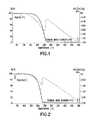
- FIG. 1is a STA plot for (NEt 2 ) 2 (HNMe)Si—Si(HNMe)(NEt 2 ) 2 .
- FIG. 2is a STA plot for (HNBu t ) 2 (HNMe)Si—Si(HNMe)(HNBu t ) 2 .
- FIG. 3is a STA plot for (HNBu t ) 2 (NH 2 )Si—Si(NH 2 )(HNBu t ) 2 .
- FIG. 4is an X-ray crystal structure of the compound (HNBu t ) 2 (NH 2 )Si—Si(NH 2 )(HNBu t ) 2 .
- the present inventionrelates to silicon precursors for CVD formation of films on substrates, such as silicon precursors for forming low k dielectric films, high k gate silicates, low temperature silicon epitaxial films, and films comprising silicon, silicon oxide, silicon oxynitride, silicon nitride, etc., as well as to corresponding processes for forming such films with such precursors.
- Disilane derivativesthat are fully substituted with alkylamino and/or dialkylamino functional groups, free of any halogen-substitutes, are found particularly suitable for low-temperature deposition of silicon nitride thin films.
- Such fully substituted disilane compoundmay be represented by the generic formula of:
- R 1 -R 12may be the same as or different from one another and each is independently selected from the group consisting of H, C 1 -C 5 alkyl, and C 3 -C 6 cycloalkyl.
- the fully substituted disilane compounds of the above formulaare advantageously characterized by a melting temperature of less than 100° C., and a vaporization temperature of less than 300° C. Moreover, such disilane compounds can be transported in vapor form at less than 300° C., with no or little ( ⁇ 1%) residual material at atmospheric pressure.
- the silicon-containing films that can be formed using such disilane precursor compoundsinclude low dielectric constant (k) thin films, high k gate silicates and silicon epitaxial films. In a particularly preferred embodiment of the invention, the films formed using such disilane precursors comprise silicon nitride.
- Preferred disilane compounds of the above-described formulainclude those characterized by a symmetrical structure in relation to the Si—Si bond, such as (NEt 2 ) 2 (HNMe)Si—Si(HNMe)(NEt 2 ) 2 , (HNBu t ) 2 (HNMe)Si—Si(HNMe)(HNBu t ) 2 , and (HNBu t ) 2 (NH 2 )Si—Si(NH 2 )(HNBu t ) 2 , etc. More preferably, such disilane compounds contain at least two alkylamino functional groups and/or two or more dialkylamino functional groups that are symmetrically distributed in relation to the Si—Si bond.
- both (HNBu t ) 2 (HNMe)Si—Si(HNMe)(HNBu t ) 2 and (HNBu t ) 2 (NH 2 )Si—Si(NH 2 )(HNBu t ) 2contain four t-butylamino functional groups that are symmetrically distributed in relation to the Si—Si bond;
- (NEt 2 ) 2 (HNMe)Si—Si(HNMe)(NEt 2 ) 2contains two methylamino functional groups and four diethylamino functional groups that are symmetrically distributed in relation to the Si—Si bond.
- FIG. 1shows the STA plot for (NEt 2 ) 2 (HNMe)Si—Si(HNMe)(NEt 2 ) 2 , which has a melting temperature of about 81.7° C., and can be transported in its vapor form completely with almost no residual material at about 300° C. at atmospheric pressure or in a flow of inert gas.
- FIG. 2is the STA plot for (HNBu t ) 2 (HNMe)Si—Si(HNMe)(HNBu t ) 2 , showing an even lower melting temperature of about 34.0° C., with only 0.55% residual material when vaporized at about 250° C. at atmospheric pressure or in a flow of inert gas.
- FIG. 3is the STA plot for (HNBu t ) 2 (NH 2 )Si—Si(NH 2 )(HNBu t ) 2 , which has a melting temperature of about 72.1° C. and can be transported in its vapor form at about 250° C., with only 0.49% residual material noted at 500° C.
- FIG. 4further shows an X-ray crystal structure of the disilane derivative compound (HNBu t ) 2 (NH 2 )Si—Si(NH 2 )(HNBu t ) 2 .
- the disilane compound (NEt 2 ) 2 (HNMe)Si—Si(HNMe)(NEt 2 ) 2can be synthesized by reacting (NEt 2 ) 2 (Cl)Si—Si(Cl)(NEt 2 ) 2 with excess amount of H 2 NMe, according to the following equations: (NE t 2 ) 2 (Cl)Si—Si(Cl)(NE t 2 ) 2 +excess H 2 NMe ⁇ (NE t 2 ) 2 (HNM e )Si—Si(HNM e )(NE t 2 ) 2 +2H 2 NM e ⁇ HCl
- a 1 L flaskwas filled with a solution comprising 500 mL diethyl ether and 20 grams (48.2 mmol) of (NEt 2 ) 2 (Cl)Si—Si(Cl)(NEt 2 ) 2 .
- H 2 NMewas bubbled into such solution.
- White precipitatewas observed during the addition of H 2 NMe.
- Approximately 20 grams of H 2 NMe (644.25 mmol)was added into the 1 L reaction flask during a ten-hour period. The resulting mixture was filtered, and all volatile materials were removed from the filtrate under vacuum conditions. The crude yield was about 90%. Either vacuum distillation or low temperature crystallization is used to purify the end product.
- the disilane compound (HNBu t ) 2 (HNMe)Si—Si(HNMe)(HNBu t ) 2can be synthesized by reacting (HNBu t ) 2 (Cl)Si—Si(Cl)(HNBu t ) 2 with about 2 molar ratio of LiN(H)Me, according to the following equations: (HNBu t ) 2 (Cl)Si—Si(Cl)(HNB u t ) 2 +2 LiN(H)M e ⁇ (HNBu t ) 2 (HNM e )Si—Si(HNM e )(HNBu t ) 2 +2LiCl
- a 250 mL flaskwas charged with a solution comprising 100 mL diethyl ether and 20.1 mL (1.6M, 32.2 mmol) of n-butyllithium hexanes solution. 1 gram of H 2 NMe was then bubbled into such solution at 0° C. White precipitate material was formed immediately. Upon completion of this addition, the 250 mL reaction flask was allowed to warm up to room temperature and was stirred for about one hour.
- the disilane compound (HNBu t ) 2 (NH 2 )Si—Si(NH 2 )(HNBu t ) 2can be synthesized by reacting (HNBu t ) 2 (Cl)Si—Si(Cl)(HNBu t ) 2 with about 2 molar ratio of LiNH 2 , according to the following equations: (HNB u t ) 2 (Cl)Si—Si(Cl)(HNB u t ) 2 +2LiNH 2 ⁇ (HNB u t ) 2 (NH 2 )Si—Si(NH 2 )(HNB u t ) 2 +2LiCl
- disilane derivative compounds of the present invention as described hereinabovecan be used, either separately or as mixtures, for low-temperature CVD deposition of various silicon-containing films, including silicon nitride thin films, consistent with the disclosure in U.S. Pat. No. 7,531,679 for “Composition and Method for Low Temperature Deposition of Silicon-Containing Films Including Silicon Nitride, Silicon Dioxide and/or Silicon-Oxynitride” filed on Nov.
- a method of forming a silicon-containing film on a substratecomprises contacting the substrate under vapor deposition conditions with a composition comprising a disilane compound that is fully substituted with alkylamino (—NHR) and/or dialkylamino (—N(R 2 )) functional groups, wherein each R is independently selected from the group consisting of C 3 -C 5 alkyl and wherein the substrate is contacted with a co-reactant selected from the group consisting of oxygen, ozone, CO 2 , nitrogen, ammonia, compounds of the formula R 3 Si—N 3 wherein each R is independently selected from C 1 -C 3 alkyl, compounds of the formula R—N ⁇ NR′ wherein each R is independently selected from C 1 -C 3 alkyl and R′ is R or H, compounds of the formula R—N ⁇ N + ⁇ NR′ wherein each R is independently selected from C 1 -C 3 alkyl and R′ is R or H, dinitrogen oxide, hydrogen, silane, disilane, haf
- the co-reactantcan be (i) oxygen, ozone or CO 2 to form low k dielectric films, (ii) oxygen or a combination of oxygen and nitrogen at deposition temperature ⁇ 600° C. to form silicon dioxide, (iii) ammonia “or A,” wherein “A” is selected from the group consisting of R 3 Si—N 3 , R—N ⁇ NR′ and R—N ⁇ N + ⁇ NR′, each R is independently selected from the group consisting of C 1 -C 3 alkyl substituents, R′ is R or H, and such co-reactant species is employed at deposition temperature ⁇ 600° C.
- silicon nitride(iv) dinitrogen oxide (nitrous oxide, N 2 O), or a mixture of nitrous oxide and ammonia, at temperature ⁇ 600° C., to form silicon oxynitride, (v) hydrogen and silane, for low temperature silicon epitaxy, and (vi) hafnium and/or zirconium sources, in the presence of oxygen and nitrous oxide, to form silicate gate structures.
- dinitrogen oxidenitrous oxide, N 2 O
- ammoniaat temperature ⁇ 600° C.
- silanefor low temperature silicon epitaxy
- hafnium and/or zirconium sourcesin the presence of oxygen and nitrous oxide
- one or more of the above-described disilane derivativesare first dissolved in a hydrocarbon solvent or a solvent system that comprises at least one hydrocarbon solvent.
- Suitable hydrocarbon solvents for the practice of the present inventioninclude, but are not limited to, alkylamines such as HN i Pr 2 , wherein i Pr is used herein as the abbreviation of isopropyl.
- Such solution containing the disilane derivative(s) of the present inventionis vaporized at a temperature that is not higher than 300° C., preferably not higher than 150° C., and more preferably about 120° C., and transported to the deposition chamber together with a carrier gas, such as helium or argon, for contact with a heated substrate surface to deposit the silicon-containing thin films.
- a carrier gassuch as helium or argon
- Silicone nitride deposition processes using one or more disilane derivatives of the present inventionare described in the following examples:
- a solution of the compound (HNEt) 3 Si—Si(HNEt) 3was prepared at a concentration of 0.4M in a hydrocarbon solvent and at a concentration of 0.036M in HN i Pr 2 . These solutions were metered at 0.0127 ml/minute and 0.167 ml/miniute, respectively into a vaporizer that was held at temperature of 120° C. and had a flow of 10 standard cubic centimeters per minute (sccm) of He as a carrier gas. The vapor was mixed with 50 sccm or 25 sccm, respectively of NH 3 in a showerhead vaporizer device that was maintained at 120° C. and thereby dispersed over the surface of a heated Si(100) wafer. The chamber pressure was maintained at 10 Torr to 60 Torr during deposition. The growth rate of the silicon nitride films ranged from 72 ⁇ /minute to 34 ⁇ /minute depending upon pressure, temperature, NH 3 rate, and precursor rate.
- a solution of the compound of Example 2, (HNBu t ) 2 (HNMe)Si—Si(HNMe)(HNBu t ) 2was prepared at a concentration of 0.4M in a hydrocarbon solvent. This solution was metered at 0.0127 ml/minute or 0.025 ml/miniute into a vaporizer that was held at temperature of 120° C. and had a flow of 10 standard cubic centimeters per minute (sccm) of He as a carrier gas. The vapor was mixed with 50 sccm or 300 sccm of NH 3 in a showerhead vaporizer device that was maintained at 120° C. and thereby dispersed over the surface of a heated Si(100) wafer. The chamber pressure was maintained at 20 Torr to 60 Torr during deposition. The growth rate of the silicon nitride films ranged from 30 ⁇ /minute to 2 ⁇ /minute depending upon pressure, temperature, NH 3 rate, and precursor rate.
- the vaporwas mixed with 38 sccm to 300 sccm of NH 3 in a showerhead vaporizer device that was maintained at 120° C. and thereby dispersed over the surface of a heated Si(100) wafer.
- the chamber pressurewas maintained at 4 Torr to 60 Torr during deposition.
- the growth rate of the silicon nitride filmsranged from 68 ⁇ /minute to 7 ⁇ /minute depending upon pressure, temperature, NH 3 rate, and precursor rate.
- a solution of two compounds: 0.0576M (HNBu t ) 2 (NH 2 )Si—Si(NH 2 )(HNBu t ) 2 , 0.0144M (HNEt) 3 Si—Si(HNEt) 3was prepared in HN i Pr 2 .
- This solutionwas metered at 0.0138 ml/minute into a vaporizer that was held at temperature of 120° C. and had a flow of 10 standard cubic centimeters per minute (sccm) of He as a carrier gas.
- the vaporwas mixed with 275 sccm of NH 3 in a showerhead vaporizer device that was maintained at 120° C. and thereby dispersed over the surface of a heated Si(100) wafer.
- the chamber pressurewas maintained at 10 Torr to 60 Torr during deposition.
- the growth rate of the silicon nitride filmsranged from 33 ⁇ /minute to 7 ⁇ /minute depending upon pressure and temperature.
Landscapes
- Chemical & Material Sciences (AREA)
- Organic Chemistry (AREA)
- Engineering & Computer Science (AREA)
- Metallurgy (AREA)
- Materials Engineering (AREA)
- Chemical Kinetics & Catalysis (AREA)
- General Chemical & Material Sciences (AREA)
- Mechanical Engineering (AREA)
- Inorganic Chemistry (AREA)
- Crystallography & Structural Chemistry (AREA)
- General Physics & Mathematics (AREA)
- Condensed Matter Physics & Semiconductors (AREA)
- Physics & Mathematics (AREA)
- Manufacturing & Machinery (AREA)
- Computer Hardware Design (AREA)
- Microelectronics & Electronic Packaging (AREA)
- Power Engineering (AREA)
- Formation Of Insulating Films (AREA)
- Chemical Vapour Deposition (AREA)
Abstract
Description

wherein R1-R12may be the same as or different from one another and each is independently selected from the group consisting of H, C1-C5alkyl, and C3-C6cycloalkyl.

wherein R1-R12may be the same as or different from one another and each is independently selected from the group consisting of H, C1-C5alkyl, and C3-C6cycloalkyl.
(NEt2)2(Cl)Si—Si(Cl)(NEt2)2+excess H2NMe→(NEt2)2(HNMe)Si—Si(HNMe)(NEt2)2+2H2NMe·HCl
(HNBut)2(Cl)Si—Si(Cl)(HNBut)2+2 LiN(H)Me→(HNBut)2(HNMe)Si—Si(HNMe)(HNBut)2+2LiCl
(HNBut)2(Cl)Si—Si(Cl)(HNBut)2+2LiNH2→(HNBut)2(NH2)Si—Si(NH2)(HNBut)2+2LiCl

In reaction scheme (C), the co-reactant can be (i) oxygen, ozone or CO2to form low k dielectric films, (ii) oxygen or a combination of oxygen and nitrogen at deposition temperature <600° C. to form silicon dioxide, (iii) ammonia “or A,” wherein “A” is selected from the group consisting of R3Si—N3, R—N═NR′ and R—N═N+═NR′, each R is independently selected from the group consisting of C1-C3alkyl substituents, R′ is R or H, and such co-reactant species is employed at deposition temperature <600° C. to form silicon nitride, (iv) dinitrogen oxide (nitrous oxide, N2O), or a mixture of nitrous oxide and ammonia, at temperature <600° C., to form silicon oxynitride, (v) hydrogen and silane, for low temperature silicon epitaxy, and (vi) hafnium and/or zirconium sources, in the presence of oxygen and nitrous oxide, to form silicate gate structures.
| TABLE 1 |
| Film composition for various deposition conditions using the precursor |
| (HNEt)3Si—Si(HNEt)3with the nitrogen source and solvent HNiPr2 |
| NH3 | HNiPr2 | T | Rate | UVAE | H | C | |||
| (sccm) | (sccm) | (° C.) | P (torr) | (Å/min) | n | (eV) | (at %) | (at %) | N/Si |
| 25 | 25 | 550 | 20 | 41 | 1.92 | 4.13 | 16.5 | 10.8 | 1.23 |
| 50 | 0 | 550 | 60 | 44 | 1.85 | 4.31 | 19.0 | 5.6 | 1.24 |
| 25 | 25 | 550 | 10 | 41 | 1.98 | 3.91 | 14.7 | 11.0 | 1.10 |
| 50 | 0 | 550 | 20 | 36 | 1.94 | 3.82 | 15.0 | 6.9 | 1.12 |
| TABLE 2 |
| Film composition for various deposition conditions using the precursor |
| (NEt2)2(HNMe)Si—Si(HNMe)(NEt2)2 |
| Rate | ||||||||
| NH3 | T | P | (Å/ | UVAE | H | C | ||
| (sccm) | (° C.) | (torr) | min) | n | (eV) | (at %) | (at %) | N/ |
| 300 | 600 | 20 | 8 | 1.96 | 5.21 | 9.5 | 1.7 | 1.36 |
| 50 | 550 | 5 | 13 | 1.99 | 4.00 | 10.0 | 8.5 | 1.20 |
| TABLE 3 |
| Film composition for various deposition conditions using the precursor |
| (HNBut)2(HNMe)Si—Si(HNMe)(HNBut)2 |
| Rate | ||||||||
| NH3 | T | P | (Å/ | UVAE | H | C | ||
| (sccm) | (° C.) | (torr) | min) | n | (eV) | (at %) | (at %) | N/ |
| 50 | 550 | 20 | 13 | 1.83 | 5.14 | 12.5 | 6.9 | 1.47 |
| TABLE 4 |
| Film composition for various deposition conditions using the precursor |
| (HNBut)2(NH2)Si—Si(NH2)(HNBut)2 |
| NH3 | HNiPr2 | T | Rate | UVAE | H | C | |||
| (sccm) | (sccm) | (° C.) | P (torr) | (Å/min) | n | (eV) | (at %) | (at %) | N/Si |
| 38 | 12 | 550 | 20 | 29 | 1.83 | 5.01 | 15.5 | 7.4 | 1.42 |
| 30 | 0 | 500 | 4 | 14 | 1.74 | 5.70 | 19.5 | 3.6 | 1.19 |
| TABLE 5 |
| Film composition for various deposition conditions using the precursor |
| (HNBut)2(NH2)Si—Si(NH2)(HNBut)2with (HNEt)3Si—Si(HNEt)3 |
| NH3 | HNiPr2 | T | Rate | UVAE | H | C | |||
| (sccm) | (sccm) | (° C.) | P (torr) | (Å/min) | n | (eV) | (at %) | (at %) | N/Si |
| 275 | 25 | 550 | 20 | 11 | 1.90 | 4.86 | 10.5 | 3.1 | 1.42 |
Claims (5)
Priority Applications (1)
| Application Number | Priority Date | Filing Date | Title |
|---|---|---|---|
| US13/028,193US8236097B2 (en) | 2002-11-14 | 2011-02-15 | Composition and method for low temperature deposition of silicon-containing films |
Applications Claiming Priority (5)
| Application Number | Priority Date | Filing Date | Title |
|---|---|---|---|
| US10/294,431US7531679B2 (en) | 2002-11-14 | 2002-11-14 | Composition and method for low temperature deposition of silicon-containing films such as films including silicon nitride, silicon dioxide and/or silicon-oxynitride |
| US10/699,079US7446217B2 (en) | 2002-11-14 | 2003-10-31 | Composition and method for low temperature deposition of silicon-containing films |
| US12/247,120US7713346B2 (en) | 2002-11-14 | 2008-10-07 | Composition and method for low temperature deposition of silicon-containing films |
| US12/777,519US7887883B2 (en) | 2002-11-14 | 2010-05-11 | Composition and method for low temperature deposition of silicon-containing films |
| US13/028,193US8236097B2 (en) | 2002-11-14 | 2011-02-15 | Composition and method for low temperature deposition of silicon-containing films |
Related Parent Applications (1)
| Application Number | Title | Priority Date | Filing Date |
|---|---|---|---|
| US12/777,519ContinuationUS7887883B2 (en) | 2002-11-14 | 2010-05-11 | Composition and method for low temperature deposition of silicon-containing films |
Publications (2)
| Publication Number | Publication Date |
|---|---|
| US20110136343A1 US20110136343A1 (en) | 2011-06-09 |
| US8236097B2true US8236097B2 (en) | 2012-08-07 |
Family
ID=32314390
Family Applications (4)
| Application Number | Title | Priority Date | Filing Date |
|---|---|---|---|
| US10/699,079Expired - LifetimeUS7446217B2 (en) | 2002-11-14 | 2003-10-31 | Composition and method for low temperature deposition of silicon-containing films |
| US12/247,120Expired - LifetimeUS7713346B2 (en) | 2002-11-14 | 2008-10-07 | Composition and method for low temperature deposition of silicon-containing films |
| US12/777,519Expired - LifetimeUS7887883B2 (en) | 2002-11-14 | 2010-05-11 | Composition and method for low temperature deposition of silicon-containing films |
| US13/028,193Expired - Fee RelatedUS8236097B2 (en) | 2002-11-14 | 2011-02-15 | Composition and method for low temperature deposition of silicon-containing films |
Family Applications Before (3)
| Application Number | Title | Priority Date | Filing Date |
|---|---|---|---|
| US10/699,079Expired - LifetimeUS7446217B2 (en) | 2002-11-14 | 2003-10-31 | Composition and method for low temperature deposition of silicon-containing films |
| US12/247,120Expired - LifetimeUS7713346B2 (en) | 2002-11-14 | 2008-10-07 | Composition and method for low temperature deposition of silicon-containing films |
| US12/777,519Expired - LifetimeUS7887883B2 (en) | 2002-11-14 | 2010-05-11 | Composition and method for low temperature deposition of silicon-containing films |
Country Status (5)
| Country | Link |
|---|---|
| US (4) | US7446217B2 (en) |
| EP (1) | EP1567531A4 (en) |
| JP (1) | JP2006517517A (en) |
| AU (1) | AU2003287710A1 (en) |
| WO (1) | WO2004044958A2 (en) |
Cited By (6)
| Publication number | Priority date | Publication date | Assignee | Title |
|---|---|---|---|---|
| US10262854B2 (en) | 2014-09-17 | 2019-04-16 | Asm Ip Holding B.V. | Deposition of SiN |
| US10395917B2 (en) | 2013-03-14 | 2019-08-27 | Asm Ip Holding B.V. | Si precursors for deposition of SiN at low temperatures |
| US10410857B2 (en) | 2015-08-24 | 2019-09-10 | Asm Ip Holding B.V. | Formation of SiN thin films |
| US10424477B2 (en) | 2013-03-14 | 2019-09-24 | Asm Ip Holding B.V. | Si precursors for deposition of SiN at low temperatures |
| US10580645B2 (en) | 2018-04-30 | 2020-03-03 | Asm Ip Holding B.V. | Plasma enhanced atomic layer deposition (PEALD) of SiN using silicon-hydrohalide precursors |
| US11996286B2 (en) | 2020-12-09 | 2024-05-28 | Asm Ip Holding B.V. | Silicon precursors for silicon nitride deposition |
Families Citing this family (51)
| Publication number | Priority date | Publication date | Assignee | Title |
|---|---|---|---|---|
| JP4116283B2 (en) | 2001-11-30 | 2008-07-09 | レール・リキード−ソシエテ・アノニム・プール・レテュード・エ・レクスプロワタシオン・デ・プロセデ・ジョルジュ・クロード | Hexakis (monohydrocarbylamino) disilane and process for producing the same |
| US7446217B2 (en)* | 2002-11-14 | 2008-11-04 | Advanced Technology Materials, Inc. | Composition and method for low temperature deposition of silicon-containing films |
| US7531679B2 (en)* | 2002-11-14 | 2009-05-12 | Advanced Technology Materials, Inc. | Composition and method for low temperature deposition of silicon-containing films such as films including silicon nitride, silicon dioxide and/or silicon-oxynitride |
| US7601860B2 (en)* | 2003-10-10 | 2009-10-13 | Advanced Technology Materials, Inc. | Composition and method for low temperature chemical vapor deposition of silicon-containing films including silicon carbonitride and silicon oxycarbonitride films |
| US7579496B2 (en)* | 2003-10-10 | 2009-08-25 | Advanced Technology Materials, Inc. | Monosilane or disilane derivatives and method for low temperature deposition of silicon-containing films using the same |
| US20050227017A1 (en)* | 2003-10-31 | 2005-10-13 | Yoshihide Senzaki | Low temperature deposition of silicon nitride |
| US7618837B2 (en) | 2004-06-29 | 2009-11-17 | Peking University | Method for fabricating high aspect ratio MEMS device with integrated circuit on the same substrate using post-CMOS process |
| US20060019032A1 (en)* | 2004-07-23 | 2006-01-26 | Yaxin Wang | Low thermal budget silicon nitride formation for advance transistor fabrication |
| US20080207005A1 (en)* | 2005-02-15 | 2008-08-28 | Freescale Semiconductor, Inc. | Wafer Cleaning After Via-Etching |
| WO2007025565A1 (en)* | 2005-09-01 | 2007-03-08 | Freescale Semiconductor, Inc. | Semiconductor device including a coupled dielectric layer and metal layer, method of fabrication thereof, and material for coupling a dielectric layer and a metal layer in a semiconductor device |
| US20090045164A1 (en)* | 2006-02-03 | 2009-02-19 | Freescale Semiconductor, Inc. | "universal" barrier cmp slurry for use with low dielectric constant interlayer dielectrics |
| US7803719B2 (en)* | 2006-02-24 | 2010-09-28 | Freescale Semiconductor, Inc. | Semiconductor device including a coupled dielectric layer and metal layer, method of fabrication thereof, and passivating coupling material comprising multiple organic components for use in a semiconductor device |
| WO2007095973A1 (en)* | 2006-02-24 | 2007-08-30 | Freescale Semiconductor, Inc. | Integrated system for semiconductor substrate processing using liquid phase metal deposition |
| JP5290146B2 (en) | 2006-04-03 | 2013-09-18 | レール・リキード−ソシエテ・アノニム・プール・レテュード・エ・レクスプロワタシオン・デ・プロセデ・ジョルジュ・クロード | PENTAKIS (DIMETHYLAMINO) DILANA PRECURSOR COMPOUND AND METHOD FOR PREPARING THE SAME |
| WO2007112780A1 (en)* | 2006-04-03 | 2007-10-11 | L'air Liquide Societe Anonyme A Directoire Et Conseil De Surveillance Pour L'etude Et L'exploitation Des Procedes Georges Claude | Method for depositing silicon nitride films and/or silicon oxynitride films by chemical vapor deposition |
| US8101788B2 (en)* | 2006-09-29 | 2012-01-24 | Air Liquide Electronics U.S. Lp | Silicon precursors and method for low temperature CVD of silicon-containing films |
| TW200831694A (en)* | 2007-01-17 | 2008-08-01 | Advanced Tech Materials | Precursor compositions for ALD/CVD of group II ruthenate thin films |
| WO2008128141A2 (en)* | 2007-04-12 | 2008-10-23 | Advanced Technology Materials, Inc. | Zirconium, hafnuim, titanium, and silicon precursors for ald/cvd |
| KR101593352B1 (en)* | 2007-06-28 | 2016-02-15 | 인티그리스, 인코포레이티드 | Precursors for silicon dioxide gap fill |
| US8501637B2 (en) | 2007-12-21 | 2013-08-06 | Asm International N.V. | Silicon dioxide thin films by ALD |
| US8298628B2 (en) | 2008-06-02 | 2012-10-30 | Air Products And Chemicals, Inc. | Low temperature deposition of silicon-containing films |
| US8772524B2 (en)* | 2008-10-20 | 2014-07-08 | Dow Corning Corporation | CVD precursors |
| JP5665289B2 (en) | 2008-10-29 | 2015-02-04 | 株式会社日立国際電気 | Semiconductor device manufacturing method, substrate processing method, and substrate processing apparatus |
| US8663735B2 (en)* | 2009-02-13 | 2014-03-04 | Advanced Technology Materials, Inc. | In situ generation of RuO4 for ALD of Ru and Ru related materials |
| DE102009001181A1 (en)* | 2009-02-26 | 2010-09-02 | Wacker Chemie Ag | Cyclic aza-silane compounds |
| US8912353B2 (en) | 2010-06-02 | 2014-12-16 | Air Products And Chemicals, Inc. | Organoaminosilane precursors and methods for depositing films comprising same |
| US8771807B2 (en) | 2011-05-24 | 2014-07-08 | Air Products And Chemicals, Inc. | Organoaminosilane precursors and methods for making and using same |
| US9070758B2 (en)* | 2011-06-20 | 2015-06-30 | Imec | CMOS compatible method for manufacturing a HEMT device and the HEMT device thereof |
| WO2013038929A1 (en)* | 2011-09-12 | 2013-03-21 | 新日鉄住金化学株式会社 | Organic electroluminescent element material having silicon-containing four membered ring structure, and organic electroluminescent element |
| WO2013177326A1 (en) | 2012-05-25 | 2013-11-28 | Advanced Technology Materials, Inc. | Silicon precursors for low temperature ald of silicon-based thin-films |
| US9978585B2 (en) | 2012-06-01 | 2018-05-22 | Versum Materials Us, Llc | Organoaminodisilane precursors and methods for depositing films comprising same |
| US9337018B2 (en)* | 2012-06-01 | 2016-05-10 | Air Products And Chemicals, Inc. | Methods for depositing films with organoaminodisilane precursors |
| US9796739B2 (en) | 2013-06-26 | 2017-10-24 | Versum Materials Us, Llc | AZA-polysilane precursors and methods for depositing films comprising same |
| JP6144161B2 (en)* | 2013-09-03 | 2017-06-07 | 株式会社日本触媒 | Silicon nitride film raw material and silicon nitride film obtained from the raw material |
| WO2015105350A1 (en)* | 2014-01-08 | 2015-07-16 | Dnf Co.,Ltd. | Novel cyclodisilazane derivative, method for preparing the same and silicon-containing thin film using the same |
| JP6340251B2 (en)* | 2014-05-30 | 2018-06-06 | 東京エレクトロン株式会社 | Method for forming SiCN film |
| US9875888B2 (en) | 2014-10-03 | 2018-01-23 | Applied Materials, Inc. | High temperature silicon oxide atomic layer deposition technology |
| KR102655396B1 (en) | 2015-02-23 | 2024-04-04 | 어플라이드 머티어리얼스, 인코포레이티드 | Cyclic sequential processes to form high quality thin films |
| JP6501560B2 (en)* | 2015-03-06 | 2019-04-17 | 東京エレクトロン株式会社 | Method and apparatus for forming silicon nitride film |
| JP6345136B2 (en)* | 2015-03-06 | 2018-06-20 | 東京エレクトロン株式会社 | Method and apparatus for forming carbon-containing silicon nitride film |
| JP2016182537A (en)* | 2015-03-25 | 2016-10-20 | 宇部興産株式会社 | Method for treating 1,2,3-triazole compounds |
| WO2016172192A1 (en)* | 2015-04-20 | 2016-10-27 | Applied Materials, Inc. | Deposition of si-h free silicon nitride |
| JP6479560B2 (en)* | 2015-05-01 | 2019-03-06 | 東京エレクトロン株式会社 | Deposition equipment |
| EP3329032B1 (en)* | 2015-07-31 | 2022-09-21 | Versum Materials US, LLC | Compositions and methods for depositing silicon nitride films |
| KR20210028742A (en)* | 2015-12-21 | 2021-03-12 | 버슘머트리얼즈 유에스, 엘엘씨 | Compositions and methods using same for deposition of silicon-containing film |
| TWI724141B (en) | 2016-03-23 | 2021-04-11 | 法商液態空氣喬治斯克勞帝方法硏究開發股份有限公司 | Si-containing film forming compositions and methods of making and using the same |
| KR102548405B1 (en)* | 2017-04-20 | 2023-06-28 | (주)디엔에프 | composition for depositing silicon-containing thin film containing a disilylamine compound and method for manufacturing a silicon-containing thin film using the same |
| JP2018101810A (en)* | 2018-03-14 | 2018-06-28 | 東京エレクトロン株式会社 | Method for forming SiCN film |
| CN113330141B (en) | 2019-01-24 | 2023-10-17 | 应用材料公司 | Method for depositing silicon nitride |
| JP7065805B2 (en)* | 2019-05-13 | 2022-05-12 | 大陽日酸株式会社 | Halogenated aminosilane compounds, thin film forming compositions and silicon-containing thin films |
| JP2025508534A (en)* | 2022-03-04 | 2025-03-26 | インテグリス・インコーポレーテッド | Method for preparing silicon-rich silicon nitride films |
Citations (24)
| Publication number | Priority date | Publication date | Assignee | Title |
|---|---|---|---|---|
| EP0521772A1 (en) | 1991-07-02 | 1993-01-07 | Elf Atochem S.A. | Process for the preparation of boron nitride ceramics and their precursors from hydrazine derivatives and precursors so produced |
| US5204141A (en) | 1991-09-18 | 1993-04-20 | Air Products And Chemicals, Inc. | Deposition of silicon dioxide films at temperatures as low as 100 degree c. by lpcvd using organodisilane sources |
| FR2693204A1 (en) | 1992-08-27 | 1994-01-07 | Atochem Elf Sa | Poly:silyl-hydrazine(s) prepn., used as coatings on e.g. ceramics, metals or metalloid(s) - comprises reacting halo-silane(s) or di:silane(s) with hydrazine(s) in presence of inert solvent |
| US5424095A (en) | 1994-03-07 | 1995-06-13 | Eniricerche S.P.A. | Ceramic vapor deposited coating using a steam-containing carrier gas and non-alkoxy silane precursors |
| JPH0822986A (en) | 1994-07-05 | 1996-01-23 | Sony Corp | Method of forming insulating film |
| US5578530A (en) | 1994-07-12 | 1996-11-26 | Sony Corporation | Manufacturing method of semiconductor device which includes forming a silicon nitride layer using a Si, N, and F containing compound |
| US5744196A (en) | 1995-01-04 | 1998-04-28 | Air Products And Chemicals, Inc. | Low temperature deposition of silicon dioxide using organosilanes |
| US5939333A (en) | 1996-05-30 | 1999-08-17 | Micron Technology, Inc. | Silicon nitride deposition method |
| US5990541A (en) | 1994-06-06 | 1999-11-23 | Sharp Kabushiki Kaisha | Semiconductor device and method of fabricating the same |
| US6013235A (en) | 1999-07-19 | 2000-01-11 | Dow Corning Corporation | Conversion of direct process high-boiling residue to monosilanes |
| JP2000080476A (en) | 1998-06-26 | 2000-03-21 | Toshiba Corp | Vapor phase growth method, vapor phase growth apparatus and ammonium halide removal apparatus |
| US20010048973A1 (en) | 1998-06-26 | 2001-12-06 | Yuusuke Sato | Ammonium halide eliminator, chemical vapor deposition system and chemical vapor deposition process |
| US6383955B1 (en) | 1998-02-05 | 2002-05-07 | Asm Japan K.K. | Silicone polymer insulation film on semiconductor substrate and method for forming the film |
| WO2003046253A1 (en) | 2001-11-30 | 2003-06-05 | L'air Liquide, Societe Anonyme A Directoire Et Conseil De Surveillance Pour L'etude Et L'exploitation Des Procedes Georges Claude | Method for depositing silicon nitride films and silicon oxynitride films by chemical vapor deposition |
| US20030129826A1 (en) | 2000-03-07 | 2003-07-10 | Werkhoven Christiaan J. | Graded thin films |
| US20040121085A1 (en) | 2002-12-20 | 2004-06-24 | Shulin Wang | Method and apparatus for forming a high quality low temperature silicon nitride film |
| EP1441042A1 (en) | 2003-01-23 | 2004-07-28 | Air Products And Chemicals, Inc. | Precursors for depositing silicon containing films and processes thereof |
| EP1149934B1 (en) | 2000-04-28 | 2005-08-03 | Asm Japan K.K. | CVD synthesis of silicon nitride materials |
| US7019159B2 (en) | 2001-11-30 | 2006-03-28 | L'air Liquide Societe Anonyme A Directoire Et Conseil De Surveillance Pour L'etude Et L'exploitation Des Procedes Georges Claude | Hexakis(monohydrocarbylamino) disilanes and method for the preparation thereof |
| US7132723B2 (en) | 2002-11-14 | 2006-11-07 | Raytheon Company | Micro electro-mechanical system device with piezoelectric thin film actuator |
| US7446217B2 (en) | 2002-11-14 | 2008-11-04 | Advanced Technology Materials, Inc. | Composition and method for low temperature deposition of silicon-containing films |
| US7531679B2 (en) | 2002-11-14 | 2009-05-12 | Advanced Technology Materials, Inc. | Composition and method for low temperature deposition of silicon-containing films such as films including silicon nitride, silicon dioxide and/or silicon-oxynitride |
| US7579496B2 (en) | 2003-10-10 | 2009-08-25 | Advanced Technology Materials, Inc. | Monosilane or disilane derivatives and method for low temperature deposition of silicon-containing films using the same |
| US7601860B2 (en) | 2003-10-10 | 2009-10-13 | Advanced Technology Materials, Inc. | Composition and method for low temperature chemical vapor deposition of silicon-containing films including silicon carbonitride and silicon oxycarbonitride films |
- 2003
- 2003-10-31USUS10/699,079patent/US7446217B2/ennot_activeExpired - Lifetime
- 2003-11-12EPEP03781915Apatent/EP1567531A4/ennot_activeWithdrawn
- 2003-11-12WOPCT/US2003/036097patent/WO2004044958A2/enactiveApplication Filing
- 2003-11-12AUAU2003287710Apatent/AU2003287710A1/ennot_activeAbandoned
- 2003-11-12JPJP2004552143Apatent/JP2006517517A/ennot_activeWithdrawn
- 2008
- 2008-10-07USUS12/247,120patent/US7713346B2/ennot_activeExpired - Lifetime
- 2010
- 2010-05-11USUS12/777,519patent/US7887883B2/ennot_activeExpired - Lifetime
- 2011
- 2011-02-15USUS13/028,193patent/US8236097B2/ennot_activeExpired - Fee Related
Patent Citations (35)
| Publication number | Priority date | Publication date | Assignee | Title |
|---|---|---|---|---|
| EP0521772A1 (en) | 1991-07-02 | 1993-01-07 | Elf Atochem S.A. | Process for the preparation of boron nitride ceramics and their precursors from hydrazine derivatives and precursors so produced |
| US5204141A (en) | 1991-09-18 | 1993-04-20 | Air Products And Chemicals, Inc. | Deposition of silicon dioxide films at temperatures as low as 100 degree c. by lpcvd using organodisilane sources |
| FR2693204A1 (en) | 1992-08-27 | 1994-01-07 | Atochem Elf Sa | Poly:silyl-hydrazine(s) prepn., used as coatings on e.g. ceramics, metals or metalloid(s) - comprises reacting halo-silane(s) or di:silane(s) with hydrazine(s) in presence of inert solvent |
| US5424095A (en) | 1994-03-07 | 1995-06-13 | Eniricerche S.P.A. | Ceramic vapor deposited coating using a steam-containing carrier gas and non-alkoxy silane precursors |
| US5990541A (en) | 1994-06-06 | 1999-11-23 | Sharp Kabushiki Kaisha | Semiconductor device and method of fabricating the same |
| JPH0822986A (en) | 1994-07-05 | 1996-01-23 | Sony Corp | Method of forming insulating film |
| US5578530A (en) | 1994-07-12 | 1996-11-26 | Sony Corporation | Manufacturing method of semiconductor device which includes forming a silicon nitride layer using a Si, N, and F containing compound |
| US5744196A (en) | 1995-01-04 | 1998-04-28 | Air Products And Chemicals, Inc. | Low temperature deposition of silicon dioxide using organosilanes |
| US5939333A (en) | 1996-05-30 | 1999-08-17 | Micron Technology, Inc. | Silicon nitride deposition method |
| US6383955B1 (en) | 1998-02-05 | 2002-05-07 | Asm Japan K.K. | Silicone polymer insulation film on semiconductor substrate and method for forming the film |
| US6410463B1 (en) | 1998-02-05 | 2002-06-25 | Asm Japan K.K. | Method for forming film with low dielectric constant on semiconductor substrate |
| JP2000080476A (en) | 1998-06-26 | 2000-03-21 | Toshiba Corp | Vapor phase growth method, vapor phase growth apparatus and ammonium halide removal apparatus |
| US20010048973A1 (en) | 1998-06-26 | 2001-12-06 | Yuusuke Sato | Ammonium halide eliminator, chemical vapor deposition system and chemical vapor deposition process |
| US6013235A (en) | 1999-07-19 | 2000-01-11 | Dow Corning Corporation | Conversion of direct process high-boiling residue to monosilanes |
| US20030129826A1 (en) | 2000-03-07 | 2003-07-10 | Werkhoven Christiaan J. | Graded thin films |
| EP1149934B1 (en) | 2000-04-28 | 2005-08-03 | Asm Japan K.K. | CVD synthesis of silicon nitride materials |
| US6936548B2 (en) | 2001-11-30 | 2005-08-30 | L'air Liquide, Societe Anonyme Pour L'etude Et, L'exploitation Des Procedes Georges Claude | Method for depositing silicon nitride films and silicon oxynitride films by chemical vapor deposition |
| WO2003046253A1 (en) | 2001-11-30 | 2003-06-05 | L'air Liquide, Societe Anonyme A Directoire Et Conseil De Surveillance Pour L'etude Et L'exploitation Des Procedes Georges Claude | Method for depositing silicon nitride films and silicon oxynitride films by chemical vapor deposition |
| US7064083B2 (en) | 2001-11-30 | 2006-06-20 | L'air Liquide, Societe Anonyme A Directoire Et Conseil De Surveillance Pour L'etude Et L'exploitation Des Procedes Georges Claude | Hexakis(monohydrocarbylamino)disilanes and method for the preparation thereof |
| US7019159B2 (en) | 2001-11-30 | 2006-03-28 | L'air Liquide Societe Anonyme A Directoire Et Conseil De Surveillance Pour L'etude Et L'exploitation Des Procedes Georges Claude | Hexakis(monohydrocarbylamino) disilanes and method for the preparation thereof |
| US7446217B2 (en) | 2002-11-14 | 2008-11-04 | Advanced Technology Materials, Inc. | Composition and method for low temperature deposition of silicon-containing films |
| US7713346B2 (en) | 2002-11-14 | 2010-05-11 | Advanced Technology Materials, Inc. | Composition and method for low temperature deposition of silicon-containing films |
| US7887883B2 (en) | 2002-11-14 | 2011-02-15 | Advanced Technology Materials, Inc. | Composition and method for low temperature deposition of silicon-containing films |
| US7132723B2 (en) | 2002-11-14 | 2006-11-07 | Raytheon Company | Micro electro-mechanical system device with piezoelectric thin film actuator |
| US20100285663A1 (en) | 2002-11-14 | 2010-11-11 | Advanced Technology Materials, Inc. | Composition and method for low temperature deposition of silicon-containing films such as films including silicon, silicon nitride, silicon dioxide and/or silicon-oxynitride |
| US7531679B2 (en) | 2002-11-14 | 2009-05-12 | Advanced Technology Materials, Inc. | Composition and method for low temperature deposition of silicon-containing films such as films including silicon nitride, silicon dioxide and/or silicon-oxynitride |
| US7786320B2 (en) | 2002-11-14 | 2010-08-31 | Advanced Technology Materials, Inc. | Composition and method for low temperature deposition of silicon-containing films such as films including silicon, silicon nitride, silicon dioxide and/or silicon-oxynitride |
| US20040121085A1 (en) | 2002-12-20 | 2004-06-24 | Shulin Wang | Method and apparatus for forming a high quality low temperature silicon nitride film |
| US20040146644A1 (en) | 2003-01-23 | 2004-07-29 | Manchao Xiao | Precursors for depositing silicon containing films and processes thereof |
| EP1441042A1 (en) | 2003-01-23 | 2004-07-28 | Air Products And Chemicals, Inc. | Precursors for depositing silicon containing films and processes thereof |
| US7601860B2 (en) | 2003-10-10 | 2009-10-13 | Advanced Technology Materials, Inc. | Composition and method for low temperature chemical vapor deposition of silicon-containing films including silicon carbonitride and silicon oxycarbonitride films |
| US7781605B2 (en) | 2003-10-10 | 2010-08-24 | Advanced Technology Materials, Inc. | Composition and method for low temperature chemical vapor deposition of silicon-containing films including silicon carbonitride and silicon oxycarbonitride films |
| US7579496B2 (en) | 2003-10-10 | 2009-08-25 | Advanced Technology Materials, Inc. | Monosilane or disilane derivatives and method for low temperature deposition of silicon-containing films using the same |
| US20100314590A1 (en) | 2003-10-10 | 2010-12-16 | Advanced Technology Materials, Inc. | Composition and method for low temperature chemical vapor deposition of silicon-containing films including silicon carbonitride and silicon oxycarbonitride films |
| US7863203B2 (en) | 2003-10-10 | 2011-01-04 | Advanced Technology Materials, Inc. | Monosilane or disilane derivatives and method for low temperature deposition of silicon-containing films using the same |
Non-Patent Citations (31)
Cited By (13)
| Publication number | Priority date | Publication date | Assignee | Title |
|---|---|---|---|---|
| US11069522B2 (en) | 2013-03-14 | 2021-07-20 | Asm Ip Holding B.V. | Si precursors for deposition of SiN at low temperatures |
| US10395917B2 (en) | 2013-03-14 | 2019-08-27 | Asm Ip Holding B.V. | Si precursors for deposition of SiN at low temperatures |
| US10424477B2 (en) | 2013-03-14 | 2019-09-24 | Asm Ip Holding B.V. | Si precursors for deposition of SiN at low temperatures |
| US11289327B2 (en) | 2013-03-14 | 2022-03-29 | Asm Ip Holding B.V. | Si precursors for deposition of SiN at low temperatures |
| US11587783B2 (en) | 2013-03-14 | 2023-02-21 | Asm Ip Holding B.V. | Si precursors for deposition of SiN at low temperatures |
| US10741386B2 (en) | 2014-09-17 | 2020-08-11 | Asm Ip Holding B.V. | Deposition of SiN |
| US10262854B2 (en) | 2014-09-17 | 2019-04-16 | Asm Ip Holding B.V. | Deposition of SiN |
| US11367613B2 (en) | 2014-09-17 | 2022-06-21 | Asm Ip Holding B.V. | Deposition of SiN |
| US10410857B2 (en) | 2015-08-24 | 2019-09-10 | Asm Ip Holding B.V. | Formation of SiN thin films |
| US11133181B2 (en) | 2015-08-24 | 2021-09-28 | Asm Ip Holding B.V. | Formation of SiN thin films |
| US11784043B2 (en) | 2015-08-24 | 2023-10-10 | ASM IP Holding, B.V. | Formation of SiN thin films |
| US10580645B2 (en) | 2018-04-30 | 2020-03-03 | Asm Ip Holding B.V. | Plasma enhanced atomic layer deposition (PEALD) of SiN using silicon-hydrohalide precursors |
| US11996286B2 (en) | 2020-12-09 | 2024-05-28 | Asm Ip Holding B.V. | Silicon precursors for silicon nitride deposition |
Also Published As
| Publication number | Publication date |
|---|---|
| US20040138489A1 (en) | 2004-07-15 |
| AU2003287710A1 (en) | 2004-06-03 |
| AU2003287710A8 (en) | 2004-06-03 |
| US7446217B2 (en) | 2008-11-04 |
| US7887883B2 (en) | 2011-02-15 |
| US20090084288A1 (en) | 2009-04-02 |
| EP1567531A2 (en) | 2005-08-31 |
| US7713346B2 (en) | 2010-05-11 |
| WO2004044958A2 (en) | 2004-05-27 |
| WO2004044958A3 (en) | 2004-08-26 |
| US20100221914A1 (en) | 2010-09-02 |
| JP2006517517A (en) | 2006-07-27 |
| US20110136343A1 (en) | 2011-06-09 |
| EP1567531A4 (en) | 2008-08-20 |
Similar Documents
| Publication | Publication Date | Title |
|---|---|---|
| US8236097B2 (en) | Composition and method for low temperature deposition of silicon-containing films | |
| US7910765B2 (en) | Composition and method for low temperature deposition of silicon-containing films such as films including silicon, silicon nitride, silicon dioxide and/or silicon-oxynitride | |
| US9783558B2 (en) | Composition and method for low temperature chemical vapor deposition of silicon-containing films including silicon carbonitride and silicon oxycarbonitride films | |
| US8242032B2 (en) | Monosilane or disilane derivatives and method for low temperature deposition of silicon-containing films using the same | |
| EP2644609B1 (en) | Precursors for depositing silicon-containing films and methods of using same | |
| US20050048204A1 (en) | Method for the fabrication of silicon nitride, silicon oxynitride, and silicon oxide films by chemical vapor deposition | |
| KR20230139282A (en) | Method of depositing a silicon-containing layer using a heterocyclic group | |
| KR20230139290A (en) | Composition for depositing a silicon-containing layer and method of depositing a silicon-containing layer using the same |
Legal Events
| Date | Code | Title | Description |
|---|---|---|---|
| STCF | Information on status: patent grant | Free format text:PATENTED CASE | |
| CC | Certificate of correction | ||
| AS | Assignment | Owner name:GOLDMAN SACHS BANK USA, AS COLLATERAL AGENT, NEW YORK Free format text:SECURITY INTEREST;ASSIGNORS:ENTEGRIS, INC.;POCO GRAPHITE, INC.;ATMI, INC.;AND OTHERS;REEL/FRAME:032815/0852 Effective date:20140430 Owner name:GOLDMAN SACHS BANK USA, AS COLLATERAL AGENT, NEW Y Free format text:SECURITY INTEREST;ASSIGNORS:ENTEGRIS, INC.;POCO GRAPHITE, INC.;ATMI, INC.;AND OTHERS;REEL/FRAME:032815/0852 Effective date:20140430 | |
| AS | Assignment | Owner name:GOLDMAN SACHS BANK USA, AS COLLATERAL AGENT, NEW YORK Free format text:SECURITY INTEREST;ASSIGNORS:ENTEGRIS, INC.;POCO GRAPHITE, INC.;ATMI, INC.;AND OTHERS;REEL/FRAME:032812/0192 Effective date:20140430 Owner name:GOLDMAN SACHS BANK USA, AS COLLATERAL AGENT, NEW Y Free format text:SECURITY INTEREST;ASSIGNORS:ENTEGRIS, INC.;POCO GRAPHITE, INC.;ATMI, INC.;AND OTHERS;REEL/FRAME:032812/0192 Effective date:20140430 | |
| AS | Assignment | Owner name:ENTEGRIS, INC., MASSACHUSETTS Free format text:ASSIGNMENT OF ASSIGNORS INTEREST;ASSIGNOR:ADVANCED TECHNOLOGY MATERIALS, INC.;REEL/FRAME:034894/0025 Effective date:20150204 | |
| FPAY | Fee payment | Year of fee payment:4 | |
| AS | Assignment | Owner name:POCO GRAPHITE, INC., MASSACHUSETTS Free format text:RELEASE BY SECURED PARTY;ASSIGNOR:GOLDMAN SACHS BANK USA, AS COLLATERAL AGENT;REEL/FRAME:047477/0032 Effective date:20181106 Owner name:ATMI PACKAGING, INC., CONNECTICUT Free format text:RELEASE BY SECURED PARTY;ASSIGNOR:GOLDMAN SACHS BANK USA, AS COLLATERAL AGENT;REEL/FRAME:047477/0032 Effective date:20181106 Owner name:ENTEGRIS, INC., MASSACHUSETTS Free format text:RELEASE BY SECURED PARTY;ASSIGNOR:GOLDMAN SACHS BANK USA, AS COLLATERAL AGENT;REEL/FRAME:047477/0032 Effective date:20181106 Owner name:ATMI, INC., CONNECTICUT Free format text:RELEASE BY SECURED PARTY;ASSIGNOR:GOLDMAN SACHS BANK USA, AS COLLATERAL AGENT;REEL/FRAME:047477/0032 Effective date:20181106 Owner name:ADVANCED TECHNOLOGY MATERIALS, INC., CONNECTICUT Free format text:RELEASE BY SECURED PARTY;ASSIGNOR:GOLDMAN SACHS BANK USA, AS COLLATERAL AGENT;REEL/FRAME:047477/0032 Effective date:20181106 Owner name:POCO GRAPHITE, INC., MASSACHUSETTS Free format text:RELEASE BY SECURED PARTY;ASSIGNOR:GOLDMAN SACHS BANK USA, AS COLLATERAL AGENT;REEL/FRAME:047477/0151 Effective date:20181106 Owner name:ENTEGRIS, INC., MASSACHUSETTS Free format text:RELEASE BY SECURED PARTY;ASSIGNOR:GOLDMAN SACHS BANK USA, AS COLLATERAL AGENT;REEL/FRAME:047477/0151 Effective date:20181106 Owner name:ATMI, INC., CONNECTICUT Free format text:RELEASE BY SECURED PARTY;ASSIGNOR:GOLDMAN SACHS BANK USA, AS COLLATERAL AGENT;REEL/FRAME:047477/0151 Effective date:20181106 Owner name:ADVANCED TECHNOLOGY MATERIALS, INC., CONNECTICUT Free format text:RELEASE BY SECURED PARTY;ASSIGNOR:GOLDMAN SACHS BANK USA, AS COLLATERAL AGENT;REEL/FRAME:047477/0151 Effective date:20181106 Owner name:ATMI PACKAGING, INC., CONNECTICUT Free format text:RELEASE BY SECURED PARTY;ASSIGNOR:GOLDMAN SACHS BANK USA, AS COLLATERAL AGENT;REEL/FRAME:047477/0151 Effective date:20181106 | |
| AS | Assignment | Owner name:GOLDMAN SACHS BANK USA, NEW YORK Free format text:SECURITY INTEREST;ASSIGNORS:ENTEGRIS, INC.;SAES PURE GAS, INC.;REEL/FRAME:048811/0679 Effective date:20181106 | |
| AS | Assignment | Owner name:MORGAN STANLEY SENIOR FUNDING, INC., MARYLAND Free format text:ASSIGNMENT OF PATENT SECURITY INTEREST RECORDED AT REEL/FRAME 048811/0679;ASSIGNOR:GOLDMAN SACHS BANK USA;REEL/FRAME:050965/0035 Effective date:20191031 | |
| FEPP | Fee payment procedure | Free format text:MAINTENANCE FEE REMINDER MAILED (ORIGINAL EVENT CODE: REM.); ENTITY STATUS OF PATENT OWNER: LARGE ENTITY | |
| LAPS | Lapse for failure to pay maintenance fees | Free format text:PATENT EXPIRED FOR FAILURE TO PAY MAINTENANCE FEES (ORIGINAL EVENT CODE: EXP.); ENTITY STATUS OF PATENT OWNER: LARGE ENTITY | |
| STCH | Information on status: patent discontinuation | Free format text:PATENT EXPIRED DUE TO NONPAYMENT OF MAINTENANCE FEES UNDER 37 CFR 1.362 | |
| FP | Lapsed due to failure to pay maintenance fee | Effective date:20200807 | |
| AS | Assignment | Owner name:TRUIST BANK, AS NOTES COLLATERAL AGENT, NORTH CAROLINA Free format text:SECURITY INTEREST;ASSIGNORS:ENTEGRIS, INC.;ENTEGRIS GP, INC.;POCO GRAPHITE, INC.;AND OTHERS;REEL/FRAME:060613/0072 Effective date:20220706 |