US8234457B2 - Dynamic adaptive flushing of cached data - Google Patents
Dynamic adaptive flushing of cached dataDownload PDFInfo
- Publication number
- US8234457B2 US8234457B2US11/480,128US48012806AUS8234457B2US 8234457 B2US8234457 B2US 8234457B2US 48012806 AUS48012806 AUS 48012806AUS 8234457 B2US8234457 B2US 8234457B2
- Authority
- US
- United States
- Prior art keywords
- data
- writeback
- writeback data
- sets
- cache memory
- Prior art date
- Legal status (The legal status is an assumption and is not a legal conclusion. Google has not performed a legal analysis and makes no representation as to the accuracy of the status listed.)
- Expired - Fee Related
Links
Images


Classifications
- G—PHYSICS
- G06—COMPUTING OR CALCULATING; COUNTING
- G06F—ELECTRIC DIGITAL DATA PROCESSING
- G06F12/00—Accessing, addressing or allocating within memory systems or architectures
- G06F12/02—Addressing or allocation; Relocation
- G06F12/08—Addressing or allocation; Relocation in hierarchically structured memory systems, e.g. virtual memory systems
- G06F12/0802—Addressing of a memory level in which the access to the desired data or data block requires associative addressing means, e.g. caches
- G06F12/0804—Addressing of a memory level in which the access to the desired data or data block requires associative addressing means, e.g. caches with main memory updating
- G—PHYSICS
- G06—COMPUTING OR CALCULATING; COUNTING
- G06F—ELECTRIC DIGITAL DATA PROCESSING
- G06F12/00—Accessing, addressing or allocating within memory systems or architectures
- G06F12/02—Addressing or allocation; Relocation
- G06F12/08—Addressing or allocation; Relocation in hierarchically structured memory systems, e.g. virtual memory systems
- G06F12/0802—Addressing of a memory level in which the access to the desired data or data block requires associative addressing means, e.g. caches
- G06F12/0866—Addressing of a memory level in which the access to the desired data or data block requires associative addressing means, e.g. caches for peripheral storage systems, e.g. disk cache
- G06F12/0868—Data transfer between cache memory and other subsystems, e.g. storage devices or host systems
- G—PHYSICS
- G06—COMPUTING OR CALCULATING; COUNTING
- G06F—ELECTRIC DIGITAL DATA PROCESSING
- G06F2212/00—Indexing scheme relating to accessing, addressing or allocation within memory systems or architectures
- G06F2212/26—Using a specific storage system architecture
- G06F2212/261—Storage comprising a plurality of storage devices
- G06F2212/262—Storage comprising a plurality of storage devices configured as RAID
- G—PHYSICS
- G06—COMPUTING OR CALCULATING; COUNTING
- G06F—ELECTRIC DIGITAL DATA PROCESSING
- G06F2212/00—Indexing scheme relating to accessing, addressing or allocation within memory systems or architectures
- G06F2212/50—Control mechanisms for virtual memory, cache or TLB
- G06F2212/502—Control mechanisms for virtual memory, cache or TLB using adaptive policy
Definitions
- the claimed inventionrelates generally to the field of data storage systems and more particularly, but not by way of limitation, to a method and apparatus directed to the dynamic adaptive flushing of cached data to a storage array.
- Storage devicesare used to access data in a fast and efficient manner. Some types of storage devices use rotatable storage media, along with one or more data transducers that write data to and subsequently read data from tracks defined on the media surfaces.
- Multi-device arrayscan employ multiple storage devices to form a consolidated memory space.
- One commonly employed format for an MDAutilizes a RAID (redundant array of independent discs) configuration, wherein input data are stored across multiple storage devices in the array.
- RAIDredundant array of independent discs
- various techniquesincluding mirroring, striping and parity code generation can be employed to enhance the integrity of the stored data.
- Preferred embodiments of the present inventionare generally directed to an apparatus and method for flushing cached writeback data to a storage array.
- sets of writeback dataare accumulated in a cache memory in an array with a view toward maintaining a substantially uniform distribution of the data across different locations of the storage array.
- the arrayed sets of dataare thereafter transferred from the cache memory to the storage array substantially at a rate at which additional sets of writeback data are provided to the cache memory by a host.
- Each set of writeback datapreferably comprises a plurality of contiguous data blocks, and are preferably written (flushed) to the storage in conjunction with the operation of a separate access command within a selected proximity range of the data with respect to the storage array.
- a stripe data descriptor (SDD)is preferably maintained for each set of writeback data in the array.
- FIG. 1generally illustrates a storage device constructed and operated in accordance with preferred embodiments of the present invention.
- FIG. 2is a functional block diagram of a network system which utilizes a number of storage devices such as illustrated in FIG. 1 .
- FIG. 3provides a general representation of a preferred architecture of the controllers of FIG. 2 .
- FIG. 4provides a functional block diagram of a selected intelligent storage processor of FIG. 3 .
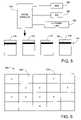
- FIG. 5generally illustrates a cache manager which operates to flush data to the storage array in accordance with preferred embodiments.
- FIG. 6represents an array of sets of writeback data maintained by the cache manager of FIG. 5 in accordance with preferred embodiments to provide a distribution of writeback data opportunities across a number of different locations of the storage array.
- FIG. 7shows a portion of the array of FIG. 6 in accordance with another preferred embodiment.
- FIG. 8is a flow chart for a WRITEBACK DATA FLUSHING routine illustrative of steps carried out in accordance with preferred embodiments.
- FIG. 1shows an exemplary storage device 100 configured to store and retrieve user data.
- the device 100is preferably characterized as a hard disc drive, although other device configurations can be readily employed as desired.
- a base deck 102mates with a top cover (not shown) to form an enclosed housing.
- a spindle motor 104is mounted within the housing to controllably rotate media 106 , preferably characterized as magnetic recording discs.
- a controllably moveable actuator 108moves an array of read/write transducers 110 adjacent tracks defined on the media surfaces through application of current to a voice coil motor (VCM) 112 .
- VCMvoice coil motor
- a flex circuit assembly 114provides electrical communication paths between the actuator 108 and device control electronics on an externally mounted printed circuit board (PCB) 116 .
- FIG. 2generally illustrates an exemplary network system 120 that advantageously incorporates a number n of the storage devices (SD) 100 to form a consolidated storage array 122 .
- Redundant controllers 124 , 126preferably operate to transfer data between the storage array 122 and a server 128 .
- the server 128in turn is connected to a fabric 130 , such as a local area network (LAN), the Internet, etc.
- LANlocal area network
- the Internetetc.
- Remote usersrespectively access the fabric 130 via personal computers (PCs) 132 , 134 , 136 .
- PCspersonal computers
- a selected usercan access the storage space 122 to write or retrieve data as desired.
- the devices 100 and the controllers 124 , 126are preferably incorporated into a multi-device array (MDA).
- MDApreferably uses one or more selected RAID (redundant array of independent discs) configurations to store data across the devices 100 .
- RAIDredundant array of independent discs
- FIG. 2shows an array controller configuration 140 such as useful in the network of FIG. 2 .
- FIG. 3sets forth two intelligent storage processors (ISPs) 142 , 144 coupled by an intermediate bus 146 (referred to as an “E BUS”).
- ISPsintelligent storage processors
- E BUSintermediate bus 146
- Each of the ISPs 142 , 144is preferably disposed in a separate integrated circuit package on a common controller board.
- the ISPs 142 , 144each respectively communicate with upstream application servers via fibre channel server links 148 , 150 , and with the storage devices 100 via fibre channel storage links 152 , 154 .
- Policy processors 156 , 158execute a real-time operating system (ROTS) for the controller 140 and communicate with the respective ISPs 142 , 144 via PCI busses 160 , 162 .
- the policy processors 156 , 158can further execute customized logic to perform sophisticated processing tasks in conjunction with the ISPs 142 , 144 for a given storage application.
- the ISPs 142 , 144 and the policy processors 156 , 158access memory modules 164 , 166 as required during operation.
- FIG. 4provides a preferred construction for a selected ISP of FIG. 3 .
- a number of function controllersserve as function controller cores (FCCs) for a number of controller operations such as host exchange, direct memory access (DMA), exclusive-or (XOR), command routing, metadata control, and disc exchange.
- FCCsfunction controller cores
- controller operationssuch as host exchange, direct memory access (DMA), exclusive-or (XOR), command routing, metadata control, and disc exchange.
- DMAdirect memory access
- XORexclusive-or
- command routingsuch as command routing, metadata control, and disc exchange.
- Each FCCpreferably contains a highly flexible feature set and interface to facilitate memory exchanges and other scheduling tasks.
- a number of list managers, denoted generally at 170are used for various data and memory management tasks during controller operation, such as cache table management, metadata maintenance, and buffer management.
- the list managers 170preferably perform well-defined albeit simple operations on memory to accomplish tasks as directed by the FCCs 168 .
- Each list managerpreferably operates as a message processor for memory access by the FCCs, and preferably executes operations defined by received messages in accordance with a defined protocol.
- the list managers 170respectively communicate with and control a number of memory modules including an exchange memory block 172 , a cache tables block 174 , buffer memory block 176 and SRAM 178 .
- the function controllers 168 and the list managers 170respectively communicate via a cross-point switch (CPS) module 180 .
- CPScross-point switch
- a selected function core of controllers 168can establish a communication pathway through the CPS 180 to a corresponding list manager 170 to communicate a status, access a memory module, or invoke a desired ISP operation.
- a selected list manager 170can communicate responses back to the function controllers 168 via the CPS 180 .
- separate data bus connectionsare preferably established between respective elements of FIG. 4 to accommodate data transfers therebetween. As will be appreciated, other configurations can readily be utilized as desired.
- a PCI interface (I/F) module 182establishes and directs transactions between the policy processor 156 and the ISP 142 .
- An E-BUS I/F module 184facilitates communications over the E-BUS 146 between FCCs and list managers of the respective ISPs 142 , 144 .
- the policy processors 156 , 158can also initiate and receive communications with other parts of the system via the E-BUS 146 as desired.
- the controller architecture of FIGS. 3 and 4advantageously provides scalable, highly functional data management and control for the array.
- stripe buffer lists (SBLs) and other metadata structuresare aligned to stripe boundaries on the storage media and reference data buffers in cache that are dedicated to storing the data associated with a disk stripe during a storage transaction.
- controller architecturepreferably employs a novel writeback data caching methodology. This generally involves the caching of data to be written to the storage devices 100 in memory, and scheduling the transfer of such writeback data to the storage devices 100 (flushing) at a later time.
- sets of contiguous blocks of writeback dataare arrayed in cache memory using a two dimensional approach that takes into account both time and locality of the data.
- a substantially uniform distribution of the cached writeback datais maintained to provide optimum opportunities to write data in conjunction with other access operations.
- sets of contiguous blocks of dataare written from the cache memory to the storage array at a rate that substantially matches a rate at which additional writeback data sets are provided to the cache memory by the host. In this way, large variations in observed host I/O transfer rates are substantially eliminated.
- the cached dataare preferably managed on a node basis by a cache manager (CM) 190 using a data structure referred to as a stripe data descriptor (SDD) 192 .
- SDDstripe data descriptor
- Each SDDholds data concerning recent and current accesses to the data with which it is associated.
- Each SDDpreferably aligns to a corresponding RAID stripe 194 (i.e., all of the data on a selected device 100 associated with a particular parity set), and conforms to a particular SBL 196 .
- Each cache node managed by the CM 190preferably references some particular SDD, with active SDD structures for a given set of logical discs (subset of the devices 100 ) being preferably linked in ascending order via a virtual block address (VBA) using a standard forward and backward linked list.
- VBAvirtual block address
- the VBA valuesare aligned with the RAID data organization using a grid system sometimes referred to as a RAID Allocation Grid System (RAGS).
- RGSRAID Allocation Grid System
- any particular collection of blocks belonging to the same RAID strip 198e.g., all of the data contributing to a particular parity set
- RSUreliable storage unit
- a bookconsists of a number of sheets and is constructed from multiple contiguous sets of blocks from different devices 100 . Based on the actual sheet and VBA, the books can be further sub-divided into zones, indicating the particular device or device set (when redundancy is employed).
- Each SDDpreferably includes variables that indicate various states of the data, including access history, locked status, last offset, last block, timestamp data (time of day, TOD), identifiers to which zone (book) the data belong, and RAID level employed.
- writeback (“dirty” data) status of the data associated with the SDDis managed in relation to dirty data, dirty buffer, dirty LRU and flushing LRU values.
- the CM 190concurrently operates to manage the writeback data processes at a number of different levels, depending on system requirements.
- a first levelgenerally involves the periodic flushing of full SDD structures when a full RAID strip 198 is detected. This can be readily carried out for a given SDD 192 based on the RAID level variable when the SDD identifies the associated data as dirty. Preferably, this involves a backward inspection to determine if enough consecutive adjacent SDD structures are sufficiently full of dirty data. If so, these SDD structures are placed on a flushing list (denoted at 199 ) and a request is made to commence flushing of the data. Flushing list status can be set using the flushing LRU value of the SDD 192 .
- Flushing smaller sets of dataare preferably handled on an SDD basis. Any SDD with dirty blocks and no locked blocks are preferably set as dirty LRU and sorted by age (e.g., time the data has spent in the cache waiting flushing). Once a particular aging is reached, the flushing LRU variable is preferably set and the flushing list 199 is updated.
- the aggressiveness of the flushing of data from the flushing listis adaptively adjusted to push out dirty data at substantially the rate that additional dirty data comes into the cache.
- the CM 190will preferably locate other ranges of dirty blocks based on the RAID level that have proximate locality; that is, blocks that are “nearby” such as in terms of seeking time or that involve access to the same RAID parity strip 199 .
- FIG. 6represents an array 200 of cached writeback data.
- the array 200is maintained by the CM 190 or other processing block of the controller.
- Each cell 202 in the array 200generally corresponds to a selected locality within the storage devices 100 , and can be organized as books, sheets and/or zones within the array. Boundaries within the devices can be selected so that, for example, each column represents a different storage device 100 and each cell in a column represents different radial bands across that device.
- each populated block 204(denoted by an “X” in FIG. 6 ) represents one (or more) groups of data blocks of varying size corresponding to a different logical or physical location within the storage devices 100 . In this way, sets of the writeback data in the cache can be pooled in anticipation of transfer to the storage array 122 .
- the array 200provides a useful format for scheduling the writeback of data across the various data devices 100 .
- the array 200is referenced to identify available blocks of writeback data that can be efficiently serviced in conjunction with the access command.
- Dirty setsare selectively added to the array 200 in an effort to maintain a substantially uniform distribution of populated cells 204 across the array 200 , and to match the rate of incoming dirty data to cache.
- the CM 190can be configured to load up a relatively large number of flushing operations to create clusters of short seeks, such as writes that progress across logical sets or physical media from ID to OD.
- the array 200 of FIG. 6can be configured to arrange the cells 202 to represent individual RAID stripes (such as 194 in FIG. 5 with a corresponding SDD 192 ), and the columns of the array 200 can correspond to columns of the aforementioned RAGS grid.
- the flushing of a particular populated cell 204 in a given rowcan be used to indicate reference to a parity (not shown in the grid) that is used by other populated cells in that same row.
- Scheduling such flushing operations at the same timemay lead to performance improvements, particularly in RAID- 5 and RAID- 6 environments, since two of the four (or six in the case of RAID- 6 ) I/O accesses for all of the populated cells in that row will access the same parity RAID stripe 194 .
- each column (or row)represents a separate storage device 100 , and each cell 202 generally corresponds to different adjacent zones, or regions, across the radial width of the media 106 of the device.
- FIG. 7One such column formatted in this manner is generally represented in FIG. 7 .
- the “W” notations in FIG. 7generally correspond to pending writeback sets of data within these various locations, and thus represent write opportunities that are distributed across the device within each cell 202 .
- the spatial locations of the W notations within each cell 202generally represents the logical or physical location of that data in the associated region.
- the W notationsdo not necessarily represent all of the writeback data sets that are available from the flushing list 199 to write to the media 106 .
- read commandswill have priority, and hence will generally be serviced prior to the servicing of write commands. However, in a write dominated environment, generally there will be a relatively larger number of write commands as compared to reads.
- One such read commandis identified by the “R” notation in FIG. 7 , and corresponds generally to the region of the media 106 from which the associated data are to be retrieved.
- the cache manager 190preferably directs the device 100 to carry out the associated read command to retrieve the data at the R notation. At the conclusion of this read operation, the cache manager 190 further preferably proceeds to have the device 100 proceed to perform one or more writeback operations that are in the general proximity of the read command (e.g., in the same cell 202 ).
- FIG. 7identifies two such writeback data sets that are serviced in this manner using a “circle-W” notation; that is, the two circle-W notation writeback flushes occur at the conclusion of the associated read command (R notation). It is not required, or even necessarily desirable, that all of the writeback data near the read command (e.g., in the cell 202 ) be flushed. However, at least some of the nearby data will be flushed and, since the transducer(s) 110 of the device 100 are in this general vicinity, these writeback data flushing operations can be carried out with reduced seek latencies.
- the cache manager 190proceeds to “backfill” the array 200 with additional writeback data sets to this same region, as such are available from the flushing list. In this way, new write commands are metered to the array 200 to substantially maintain a uniform distribution of writeback data opportunities across the various radial width of the media 106 .
- the cache manager 190generally operates to flush writeback data as before. However, as each new read command is issued, priority is given to the read command and one or more additional writeback sets are flushed from the general proximity of the read command.
- the cache manager 190operates to maintain a selected ratio of “Ws” to “Rs” in the array 200 for each device 100 , such as no more than 30 Ws and no more than two Rs pending at any given time (for a total of 32 “slots” for queued commands). Other ratios can readily be used, however. The ratios can also be adjusted over time in relation to burst changes in the read/write command mix experienced by the cache manager 190 .
- FIG. 8sets forth a WRITEBACK DATA FLUSHING routine 300 , generally representative of steps carried out in accordance with preferred embodiments of the present invention.
- the systemis initially configured at step 302 .
- thiswill include initial identification of the various boundaries for the flushing list(s) 199 and corresponding array(s) 200 to cover the physical domain of the storage devices 100 .
- different arrays and listscan be maintained for appropriate subsets of the storage space, or a single, consolidated list/array can be maintained.
- Normal system operationnext commences, and this includes the periodic provision of writeback (dirty) data to cache memory as shown at step 304 .
- writeback datawill primarily arise from data write operations from a host such as PCs 132 , 134 , 136 in FIG. 1 , in which case the controller 124 will preferably store the writeback data in a selected cache location (such as 176 in FIG. 4 ) and provide a write complete signal back to the initiating device.
- the writeback datacan alternatively comprise internally generated writes such as system status data, selected memory backups, metadata, etc.
- An SDD 192will preferably be updated for the associated writeback data as shown by step 306 .
- the dirty data and dirty buffers valuesmay initially be set to identify the data as dirty.
- the data setwill subsequently be moved to the flushing list 199 in relation to a number of factors as discussed above including relation of the data to a full strip 198 , aging, and rate of ingress of additional data into cache.
- the array 200is correspondingly populated at step 308 to identify sets of contiguous data blocks available for flushing in response to movement of said blocks to the flushing list 199 .
- step 310selected sets of the writeback data are flushed to the storage devices 100 . This preferably occurs in conjunction with other proximate access operations, although larger sequential flushing operations can also be scheduled across the devices 100 .
- the CM 190 or other processwill preferably operate to maintain a substantially uniform distribution of the available writeback data blocks in relation to the rate at which further cached writeback data are introduced to the cache memory.
- the various preferred embodiments discussed hereinprovide advantages over the prior art.
- the disclosed methodologyis dynamic in that both time and locality are factored in to the flushing algorithm to provide the efficient flushing of data to the storage devices 100 .
- the methodologyis further adaptive to substantially match the rate at which additional dirty data are introduced to the cache memory.
- the sets of dirty data in cache memorywill be selectively metered to the array 200 and from the array 200 to the storage discs 100 to maintain a substantially level loading. In this way, significant variations in host I/O rates are avoided.
Landscapes
- Engineering & Computer Science (AREA)
- Theoretical Computer Science (AREA)
- Physics & Mathematics (AREA)
- General Engineering & Computer Science (AREA)
- General Physics & Mathematics (AREA)
- Memory System Of A Hierarchy Structure (AREA)
Abstract
Description
Claims (21)
Priority Applications (2)
| Application Number | Priority Date | Filing Date | Title |
|---|---|---|---|
| US11/480,128US8234457B2 (en) | 2006-06-30 | 2006-06-30 | Dynamic adaptive flushing of cached data |
| JP2007172478AJP2008016024A (en) | 2006-06-30 | 2007-06-29 | Dynamic adaptive flushing of cached data |
Applications Claiming Priority (1)
| Application Number | Priority Date | Filing Date | Title |
|---|---|---|---|
| US11/480,128US8234457B2 (en) | 2006-06-30 | 2006-06-30 | Dynamic adaptive flushing of cached data |
Publications (2)
| Publication Number | Publication Date |
|---|---|
| US20080005478A1 US20080005478A1 (en) | 2008-01-03 |
| US8234457B2true US8234457B2 (en) | 2012-07-31 |
Family
ID=38878227
Family Applications (1)
| Application Number | Title | Priority Date | Filing Date |
|---|---|---|---|
| US11/480,128Expired - Fee RelatedUS8234457B2 (en) | 2006-06-30 | 2006-06-30 | Dynamic adaptive flushing of cached data |
Country Status (2)
| Country | Link |
|---|---|
| US (1) | US8234457B2 (en) |
| JP (1) | JP2008016024A (en) |
Cited By (1)
| Publication number | Priority date | Publication date | Assignee | Title |
|---|---|---|---|---|
| US20090327589A1 (en)* | 2008-06-25 | 2009-12-31 | Stec, Inc. | Table journaling in flash storage devices |
Families Citing this family (7)
| Publication number | Priority date | Publication date | Assignee | Title |
|---|---|---|---|---|
| US8357048B2 (en)* | 2009-09-29 | 2013-01-22 | Cleversafe, Inc. | Interactive gaming utilizing a dispersed storage network |
| WO2008149657A1 (en)* | 2007-06-05 | 2008-12-11 | Nec Corporation | I/o control system, i/o control method, and i/o control program |
| US9081686B2 (en)* | 2012-11-19 | 2015-07-14 | Vmware, Inc. | Coordinated hypervisor staging of I/O data for storage devices on external cache devices |
| EP2765528B1 (en) | 2013-02-11 | 2018-11-14 | dSPACE digital signal processing and control engineering GmbH | Unrestricted access to signal values of an FPGA during runtime |
| EP2954440B1 (en)* | 2013-02-11 | 2022-01-12 | dSPACE digital signal processing and control engineering GmbH | Alteration of a signal value for an fpga at runtime |
| CN110058786B (en)* | 2018-01-18 | 2022-12-02 | 伊姆西Ip控股有限责任公司 | Method, apparatus and computer program product for controlling write requests in a storage system |
| US12298912B1 (en)* | 2023-11-14 | 2025-05-13 | Qualcomm Incorporated | Enhanced write buffer flush scheme for memory devices with high density storage memory architecture |
Citations (27)
| Publication number | Priority date | Publication date | Assignee | Title |
|---|---|---|---|---|
| US5257352A (en) | 1989-07-05 | 1993-10-26 | Hitachi, Ltd. | Input/output control method and system |
| US5581729A (en)* | 1995-03-31 | 1996-12-03 | Sun Microsystems, Inc. | Parallelized coherent read and writeback transaction processing system for use in a packet switched cache coherent multiprocessor system |
| US5829018A (en) | 1994-10-25 | 1998-10-27 | International Business Machines Corporation | Apparatus and method for writing data from a cache to a storage device |
| US5875455A (en) | 1994-06-10 | 1999-02-23 | Matsushita Electric Industrial Co., Ltd. | Information recording and reproducing apparatus merging sequential recording requests into a single recording request, and method of data caching for such apparatus |
| US5926834A (en)* | 1997-05-29 | 1999-07-20 | International Business Machines Corporation | Virtual data storage system with an overrun-resistant cache using an adaptive throttle based upon the amount of cache free space |
| US6057789A (en)* | 1998-10-29 | 2000-05-02 | Neomagic Corp. | Re-synchronization of independently-clocked audio streams by dynamically switching among 3 ratios for sampling-rate-conversion |
| US6189080B1 (en)* | 1996-09-20 | 2001-02-13 | Emc Corporation | Minimum read rate throughput in a disk cache system |
| US6272600B1 (en)* | 1996-11-15 | 2001-08-07 | Hyundai Electronics America | Memory request reordering in a data processing system |
| US20020078303A1 (en) | 2000-12-18 | 2002-06-20 | Rozario Ranjit J. | Free memory manager scheme and cache |
| US6552923B2 (en)* | 2000-06-13 | 2003-04-22 | Texas Instruments Incorporated | SRAM with write-back on read |
| US6567888B2 (en) | 1998-06-30 | 2003-05-20 | Emc Corporation | Method and apparatus for efficiently destaging data from a cache to two or more non-contiguous storage locations |
| US6629211B2 (en) | 2001-04-20 | 2003-09-30 | International Business Machines Corporation | Method and system for improving raid controller performance through adaptive write back/write through caching |
| US6671766B1 (en) | 2000-01-07 | 2003-12-30 | Storage Technology Corporation | Method and system for implementing memory efficient track aging |
| US20040019740A1 (en)* | 2002-07-25 | 2004-01-29 | Hitachi, Ltd. | Destaging method for storage apparatus system, and disk control apparatus, storage apparatus system and program |
| US20040024971A1 (en) | 2000-09-21 | 2004-02-05 | Zohar Bogin | Method and apparatus for write cache flush and fill mechanisms |
| US6738865B1 (en) | 2000-06-09 | 2004-05-18 | International Business Machines Corporation | Method, system, and program for demoting data from cache based on least recently accessed and least frequently accessed data |
| US6789163B2 (en) | 2001-09-17 | 2004-09-07 | Seagate Technology Llc | Optimizing data transfer performance through partial write command purging in a disc drive |
| US20040205297A1 (en) | 2003-04-14 | 2004-10-14 | Bearden Brian S. | Method of cache collision avoidance in the presence of a periodic cache aging algorithm |
| US6868439B2 (en) | 2002-04-04 | 2005-03-15 | Hewlett-Packard Development Company, L.P. | System and method for supervising use of shared storage by multiple caching servers physically connected through a switching router to said shared storage via a robust high speed connection |
| US6928518B2 (en) | 2001-11-01 | 2005-08-09 | Sun Microsystems, Inc. | Disk drive employing adaptive flushing of a write cache |
| US20050182906A1 (en)* | 2004-02-18 | 2005-08-18 | Paresh Chatterjee | Systems and methods for cache synchronization between redundant storage controllers |
| US6978325B2 (en) | 2002-08-29 | 2005-12-20 | International Business Machines Corporation | Transferring data in virtual tape server, involves determining availability of small chain of data, if large chain is not available while transferring data to physical volumes in peak mode |
| US7028297B2 (en) | 2000-11-17 | 2006-04-11 | Aristos Logic Corporation | System and method of scalable transaction processing |
| US20060143407A1 (en)* | 2004-12-29 | 2006-06-29 | Lsi Logic Corporation | Methods and structure for improved storage system performance with write-back caching for disk drives |
| US20060248308A1 (en)* | 2005-04-27 | 2006-11-02 | Dot Hill Systems Corp. | Multiple mode controller method and apparatus |
| US7171516B2 (en)* | 2003-09-29 | 2007-01-30 | International Business Machines Corporation | Increasing through-put of a storage controller by autonomically adjusting host delay |
| US7734854B2 (en)* | 2008-01-04 | 2010-06-08 | International Business Machines Corporation | Device, system, and method of handling transactions |
Family Cites Families (38)
| Publication number | Priority date | Publication date | Assignee | Title |
|---|---|---|---|---|
| US1485235A (en)* | 1923-09-14 | 1924-02-26 | Mauss Wilhelm | Centrifugal separator and the like |
| BE366538A (en)* | 1929-01-04 | |||
| US2291117A (en)* | 1939-12-29 | 1942-07-28 | Laval Separator Co De | Centrifugal separator |
| US2688437A (en)* | 1947-12-04 | 1954-09-07 | Saint Gobain | Centrifugal separator |
| US3369742A (en)* | 1965-11-30 | 1968-02-20 | Carl W. Weiland | Discharge valve for centrifuge |
| FR1568746A (en)* | 1967-06-21 | 1969-05-30 | ||
| CH514358A (en)* | 1969-08-08 | 1971-10-31 | Termomeccanica Italiana Spa | Device for centrifugal separation of the two constituents with different density of an emulsion |
| CS153120B1 (en)* | 1971-01-18 | 1974-02-25 | ||
| US3791575A (en)* | 1971-08-30 | 1974-02-12 | Garrett Corp | Centrifugal separator discharge control system |
| US3797736A (en)* | 1972-04-07 | 1974-03-19 | Westfalia Separator Ag | Method and apparatus for controlling the concentration factor of a discharge |
| FR2180589B1 (en)* | 1972-04-21 | 1975-03-21 | Loison Robert | |
| US3814307A (en)* | 1973-01-12 | 1974-06-04 | Standard Oil Co | Centrifugal clarifier |
| US3810347A (en)* | 1973-01-16 | 1974-05-14 | Signal Oil & Gas Co | Centrifugal separator for three phase mixture |
| FR2268565B2 (en)* | 1974-04-25 | 1976-10-15 | Loison Robert | |
| US3930606A (en)* | 1974-05-20 | 1976-01-06 | Rca Corporation | Method and apparatus for securing wires to connector terminals |
| CH584150A5 (en)* | 1974-09-02 | 1977-01-31 | Escher Wyss Ag | |
| DE2501924C3 (en)* | 1975-01-18 | 1981-03-26 | Westfalia Separator Ag, 59302 Oelde | Solid bowl centrifuge |
| US4010891A (en)* | 1976-01-08 | 1977-03-08 | Burmah Oil & Gas Company | Vapor removal apparatus for oil/water separator |
| CS188429B1 (en)* | 1976-02-12 | 1979-03-30 | Jan Putterlik | Method of the automatic control of the discharging of the concentrated fraction from from the centrifuge rotor and device for executing the same |
| FR2532198B1 (en)* | 1982-08-27 | 1985-06-21 | Bertin & Cie | ENERGY RECOVERY CENTRIFUGE |
| JPS6391761A (en)* | 1986-10-06 | 1988-04-22 | Alps Electric Co Ltd | Cache memory control method |
| JPH05100954A (en)* | 1991-10-09 | 1993-04-23 | Hokkaido Nippon Denki Software Kk | Cache buffer processing control system |
| JP3407317B2 (en)* | 1991-11-28 | 2003-05-19 | 株式会社日立製作所 | Storage device using flash memory |
| JPH0855072A (en)* | 1994-08-12 | 1996-02-27 | Matsushita Electric Ind Co Ltd | Network system, data processing system, and data storage method |
| US5908376A (en)* | 1997-09-11 | 1999-06-01 | Costner Industries Nevada, Inc. | Self-cleaning rotor for a centrifugal separator |
| US6108745A (en)* | 1997-10-31 | 2000-08-22 | Hewlett-Packard Company | Fast and compact address bit routing scheme that supports various DRAM bank sizes and multiple interleaving schemes |
| JPH11328029A (en)* | 1998-05-18 | 1999-11-30 | Olympus Optical Co Ltd | Information recording and reproducing device |
| US6312610B1 (en)* | 1998-07-13 | 2001-11-06 | Phase Inc. | Density screening outer wall transport method for fluid separation devices |
| US6719681B2 (en)* | 1999-08-06 | 2004-04-13 | Econova, Inc. | Methods for centrifugally separating mixed components of a fluid stream |
| DE10114598A1 (en)* | 2001-03-23 | 2002-10-02 | Aventis Pharma Gmbh | CIP-compliant design of a horizontal centrifuge with a solid jacket drum |
| JP2003318947A (en)* | 2002-04-23 | 2003-11-07 | Mitsubishi Electric Corp | Switching device using multi-layer memory |
| JP2004213470A (en)* | 2003-01-07 | 2004-07-29 | Nec Corp | Disk array device, and data writing method for disk array device |
| US7320750B2 (en)* | 2003-03-11 | 2008-01-22 | Phase Inc. | Centrifuge with controlled discharge of dense material |
| SE528387C2 (en)* | 2005-03-08 | 2006-10-31 | Alfa Laval Corp Ab | Centrifugal separator and method for separating a product into at least a relatively heavy phase and a relatively light phase |
| US20080041772A1 (en)* | 2006-08-17 | 2008-02-21 | Gambro Bct, Inc. | Blood Processing Apparatus with Robust Outflow Process Control |
| US20080272067A1 (en)* | 2007-05-01 | 2008-11-06 | Cavaliere William A | Methods and Apparatus for Classification of Suspended Materials |
| GB0724572D0 (en)* | 2007-12-17 | 2008-01-30 | Specialist Process Technologie | A separation device |
| US20110263405A1 (en)* | 2010-04-22 | 2011-10-27 | Specialist Process Technologies Limited | Separator |
- 2006
- 2006-06-30USUS11/480,128patent/US8234457B2/ennot_activeExpired - Fee Related
- 2007
- 2007-06-29JPJP2007172478Apatent/JP2008016024A/enactivePending
Patent Citations (27)
| Publication number | Priority date | Publication date | Assignee | Title |
|---|---|---|---|---|
| US5257352A (en) | 1989-07-05 | 1993-10-26 | Hitachi, Ltd. | Input/output control method and system |
| US5875455A (en) | 1994-06-10 | 1999-02-23 | Matsushita Electric Industrial Co., Ltd. | Information recording and reproducing apparatus merging sequential recording requests into a single recording request, and method of data caching for such apparatus |
| US5829018A (en) | 1994-10-25 | 1998-10-27 | International Business Machines Corporation | Apparatus and method for writing data from a cache to a storage device |
| US5581729A (en)* | 1995-03-31 | 1996-12-03 | Sun Microsystems, Inc. | Parallelized coherent read and writeback transaction processing system for use in a packet switched cache coherent multiprocessor system |
| US6189080B1 (en)* | 1996-09-20 | 2001-02-13 | Emc Corporation | Minimum read rate throughput in a disk cache system |
| US6272600B1 (en)* | 1996-11-15 | 2001-08-07 | Hyundai Electronics America | Memory request reordering in a data processing system |
| US5926834A (en)* | 1997-05-29 | 1999-07-20 | International Business Machines Corporation | Virtual data storage system with an overrun-resistant cache using an adaptive throttle based upon the amount of cache free space |
| US6567888B2 (en) | 1998-06-30 | 2003-05-20 | Emc Corporation | Method and apparatus for efficiently destaging data from a cache to two or more non-contiguous storage locations |
| US6057789A (en)* | 1998-10-29 | 2000-05-02 | Neomagic Corp. | Re-synchronization of independently-clocked audio streams by dynamically switching among 3 ratios for sampling-rate-conversion |
| US6671766B1 (en) | 2000-01-07 | 2003-12-30 | Storage Technology Corporation | Method and system for implementing memory efficient track aging |
| US6738865B1 (en) | 2000-06-09 | 2004-05-18 | International Business Machines Corporation | Method, system, and program for demoting data from cache based on least recently accessed and least frequently accessed data |
| US6552923B2 (en)* | 2000-06-13 | 2003-04-22 | Texas Instruments Incorporated | SRAM with write-back on read |
| US20040024971A1 (en) | 2000-09-21 | 2004-02-05 | Zohar Bogin | Method and apparatus for write cache flush and fill mechanisms |
| US7028297B2 (en) | 2000-11-17 | 2006-04-11 | Aristos Logic Corporation | System and method of scalable transaction processing |
| US20020078303A1 (en) | 2000-12-18 | 2002-06-20 | Rozario Ranjit J. | Free memory manager scheme and cache |
| US6629211B2 (en) | 2001-04-20 | 2003-09-30 | International Business Machines Corporation | Method and system for improving raid controller performance through adaptive write back/write through caching |
| US6789163B2 (en) | 2001-09-17 | 2004-09-07 | Seagate Technology Llc | Optimizing data transfer performance through partial write command purging in a disc drive |
| US6928518B2 (en) | 2001-11-01 | 2005-08-09 | Sun Microsystems, Inc. | Disk drive employing adaptive flushing of a write cache |
| US6868439B2 (en) | 2002-04-04 | 2005-03-15 | Hewlett-Packard Development Company, L.P. | System and method for supervising use of shared storage by multiple caching servers physically connected through a switching router to said shared storage via a robust high speed connection |
| US20040019740A1 (en)* | 2002-07-25 | 2004-01-29 | Hitachi, Ltd. | Destaging method for storage apparatus system, and disk control apparatus, storage apparatus system and program |
| US6978325B2 (en) | 2002-08-29 | 2005-12-20 | International Business Machines Corporation | Transferring data in virtual tape server, involves determining availability of small chain of data, if large chain is not available while transferring data to physical volumes in peak mode |
| US20040205297A1 (en) | 2003-04-14 | 2004-10-14 | Bearden Brian S. | Method of cache collision avoidance in the presence of a periodic cache aging algorithm |
| US7171516B2 (en)* | 2003-09-29 | 2007-01-30 | International Business Machines Corporation | Increasing through-put of a storage controller by autonomically adjusting host delay |
| US20050182906A1 (en)* | 2004-02-18 | 2005-08-18 | Paresh Chatterjee | Systems and methods for cache synchronization between redundant storage controllers |
| US20060143407A1 (en)* | 2004-12-29 | 2006-06-29 | Lsi Logic Corporation | Methods and structure for improved storage system performance with write-back caching for disk drives |
| US20060248308A1 (en)* | 2005-04-27 | 2006-11-02 | Dot Hill Systems Corp. | Multiple mode controller method and apparatus |
| US7734854B2 (en)* | 2008-01-04 | 2010-06-08 | International Business Machines Corporation | Device, system, and method of handling transactions |
Cited By (2)
| Publication number | Priority date | Publication date | Assignee | Title |
|---|---|---|---|---|
| US20090327589A1 (en)* | 2008-06-25 | 2009-12-31 | Stec, Inc. | Table journaling in flash storage devices |
| US9311006B2 (en)* | 2008-06-25 | 2016-04-12 | Hgst Technologies Santa Ana, Inc. | Table journaling in flash storage devices |
Also Published As
| Publication number | Publication date |
|---|---|
| US20080005478A1 (en) | 2008-01-03 |
| JP2008016024A (en) | 2008-01-24 |
Similar Documents
| Publication | Publication Date | Title |
|---|---|---|
| US8363519B2 (en) | Hot data zones | |
| US7743216B2 (en) | Predicting accesses to non-requested data | |
| US8234457B2 (en) | Dynamic adaptive flushing of cached data | |
| US7996623B2 (en) | Read ahead storage control | |
| US7761659B2 (en) | Wave flushing of cached writeback data to a storage array | |
| US7444541B2 (en) | Failover and failback of write cache data in dual active controllers | |
| US7484050B2 (en) | High-density storage systems using hierarchical interconnect | |
| US7577778B2 (en) | Expandable storage apparatus for blade server system | |
| US7590800B2 (en) | 2D dynamic adaptive data caching | |
| US8244975B2 (en) | Command queue ordering by flipping active write zones | |
| JP3987295B2 (en) | Processing optimization method, computer, and storage device | |
| US7890696B2 (en) | Command queue ordering with directional and floating write bands | |
| US8745326B2 (en) | Request priority seek manager | |
| JP2005267038A (en) | Operation method of storage system | |
| CN102164165B (en) | Management method and device for network storage system | |
| CN102135862B (en) | Disk storage system and data access method thereof | |
| US6954825B2 (en) | Disk subsystem | |
| US6868438B2 (en) | Storage system, disk control cluster and a method of increasing of disk control cluster | |
| US20090204760A1 (en) | Storage apparatus, relay device, and method of controlling operating state | |
| TW200540623A (en) | System and method for drive recovery following a drive failure | |
| US20040148462A1 (en) | Storage system using fast storage and log-structured storage | |
| US20080005385A1 (en) | Passive mirroring through concurrent transfer of data to multiple target devices | |
| JP2009070489A (en) | Storage device, control method therefor, and disk device | |
| US20080126789A1 (en) | Method and Apparatus for Generating an Optimal Number of Spare Devices Within a RAID Storage System Having Multiple Storage Device Technology Classes | |
| JPH08171462A (en) | Parity information storage method for disk array device |
Legal Events
| Date | Code | Title | Description |
|---|---|---|---|
| AS | Assignment | Owner name:SEAGATE TECHNOLOGY LLC, CALIFORNIA Free format text:ASSIGNMENT OF ASSIGNORS INTEREST;ASSIGNORS:LUBBERS, CLARK E.;WALKER, MICHAEL D.;DECENZO, DAVID P.;REEL/FRAME:018077/0441;SIGNING DATES FROM 20060626 TO 20060629 Owner name:SEAGATE TECHNOLOGY LLC, CALIFORNIA Free format text:ASSIGNMENT OF ASSIGNORS INTEREST;ASSIGNORS:LUBBERS, CLARK E.;WALKER, MICHAEL D.;DECENZO, DAVID P.;SIGNING DATES FROM 20060626 TO 20060629;REEL/FRAME:018077/0441 | |
| AS | Assignment | Owner name:WELLS FARGO BANK, NATIONAL ASSOCIATION, AS COLLATERAL AGENT AND SECOND PRIORITY REPRESENTATIVE, CALIFORNIA Free format text:SECURITY AGREEMENT;ASSIGNORS:MAXTOR CORPORATION;SEAGATE TECHNOLOGY LLC;SEAGATE TECHNOLOGY INTERNATIONAL;REEL/FRAME:022757/0017 Effective date:20090507 Owner name:JPMORGAN CHASE BANK, N.A., AS ADMINISTRATIVE AGENT AND FIRST PRIORITY REPRESENTATIVE, NEW YORK Free format text:SECURITY AGREEMENT;ASSIGNORS:MAXTOR CORPORATION;SEAGATE TECHNOLOGY LLC;SEAGATE TECHNOLOGY INTERNATIONAL;REEL/FRAME:022757/0017 Effective date:20090507 Owner name:JPMORGAN CHASE BANK, N.A., AS ADMINISTRATIVE AGENT Free format text:SECURITY AGREEMENT;ASSIGNORS:MAXTOR CORPORATION;SEAGATE TECHNOLOGY LLC;SEAGATE TECHNOLOGY INTERNATIONAL;REEL/FRAME:022757/0017 Effective date:20090507 Owner name:WELLS FARGO BANK, NATIONAL ASSOCIATION, AS COLLATE Free format text:SECURITY AGREEMENT;ASSIGNORS:MAXTOR CORPORATION;SEAGATE TECHNOLOGY LLC;SEAGATE TECHNOLOGY INTERNATIONAL;REEL/FRAME:022757/0017 Effective date:20090507 | |
| AS | Assignment | Owner name:SEAGATE TECHNOLOGY INTERNATIONAL, CALIFORNIA Free format text:RELEASE;ASSIGNOR:JPMORGAN CHASE BANK, N.A., AS ADMINISTRATIVE AGENT;REEL/FRAME:025662/0001 Effective date:20110114 Owner name:MAXTOR CORPORATION, CALIFORNIA Free format text:RELEASE;ASSIGNOR:JPMORGAN CHASE BANK, N.A., AS ADMINISTRATIVE AGENT;REEL/FRAME:025662/0001 Effective date:20110114 Owner name:SEAGATE TECHNOLOGY HDD HOLDINGS, CALIFORNIA Free format text:RELEASE;ASSIGNOR:JPMORGAN CHASE BANK, N.A., AS ADMINISTRATIVE AGENT;REEL/FRAME:025662/0001 Effective date:20110114 Owner name:SEAGATE TECHNOLOGY LLC, CALIFORNIA Free format text:RELEASE;ASSIGNOR:JPMORGAN CHASE BANK, N.A., AS ADMINISTRATIVE AGENT;REEL/FRAME:025662/0001 Effective date:20110114 | |
| AS | Assignment | Owner name:THE BANK OF NOVA SCOTIA, AS ADMINISTRATIVE AGENT, CANADA Free format text:SECURITY AGREEMENT;ASSIGNOR:SEAGATE TECHNOLOGY LLC;REEL/FRAME:026010/0350 Effective date:20110118 Owner name:THE BANK OF NOVA SCOTIA, AS ADMINISTRATIVE AGENT, Free format text:SECURITY AGREEMENT;ASSIGNOR:SEAGATE TECHNOLOGY LLC;REEL/FRAME:026010/0350 Effective date:20110118 | |
| STCF | Information on status: patent grant | Free format text:PATENTED CASE | |
| AS | Assignment | Owner name:SEAGATE TECHNOLOGY INTERNATIONAL, CAYMAN ISLANDS Free format text:TERMINATION AND RELEASE OF SECURITY INTEREST IN PATENT RIGHTS;ASSIGNOR:WELLS FARGO BANK, NATIONAL ASSOCIATION, AS COLLATERAL AGENT AND SECOND PRIORITY REPRESENTATIVE;REEL/FRAME:030833/0001 Effective date:20130312 Owner name:SEAGATE TECHNOLOGY LLC, CALIFORNIA Free format text:TERMINATION AND RELEASE OF SECURITY INTEREST IN PATENT RIGHTS;ASSIGNOR:WELLS FARGO BANK, NATIONAL ASSOCIATION, AS COLLATERAL AGENT AND SECOND PRIORITY REPRESENTATIVE;REEL/FRAME:030833/0001 Effective date:20130312 Owner name:EVAULT INC. (F/K/A I365 INC.), CALIFORNIA Free format text:TERMINATION AND RELEASE OF SECURITY INTEREST IN PATENT RIGHTS;ASSIGNOR:WELLS FARGO BANK, NATIONAL ASSOCIATION, AS COLLATERAL AGENT AND SECOND PRIORITY REPRESENTATIVE;REEL/FRAME:030833/0001 Effective date:20130312 Owner name:SEAGATE TECHNOLOGY US HOLDINGS, INC., CALIFORNIA Free format text:TERMINATION AND RELEASE OF SECURITY INTEREST IN PATENT RIGHTS;ASSIGNOR:WELLS FARGO BANK, NATIONAL ASSOCIATION, AS COLLATERAL AGENT AND SECOND PRIORITY REPRESENTATIVE;REEL/FRAME:030833/0001 Effective date:20130312 | |
| FPAY | Fee payment | Year of fee payment:4 | |
| FEPP | Fee payment procedure | Free format text:MAINTENANCE FEE REMINDER MAILED (ORIGINAL EVENT CODE: REM.); ENTITY STATUS OF PATENT OWNER: LARGE ENTITY | |
| LAPS | Lapse for failure to pay maintenance fees | Free format text:PATENT EXPIRED FOR FAILURE TO PAY MAINTENANCE FEES (ORIGINAL EVENT CODE: EXP.); ENTITY STATUS OF PATENT OWNER: LARGE ENTITY | |
| STCH | Information on status: patent discontinuation | Free format text:PATENT EXPIRED DUE TO NONPAYMENT OF MAINTENANCE FEES UNDER 37 CFR 1.362 | |
| FP | Lapsed due to failure to pay maintenance fee | Effective date:20200731 | |
| AS | Assignment | Owner name:SEAGATE TECHNOLOGY PUBLIC LIMITED COMPANY, CALIFORNIA Free format text:RELEASE BY SECURED PARTY;ASSIGNOR:THE BANK OF NOVA SCOTIA;REEL/FRAME:072193/0001 Effective date:20250303 Owner name:SEAGATE TECHNOLOGY, CALIFORNIA Free format text:RELEASE BY SECURED PARTY;ASSIGNOR:THE BANK OF NOVA SCOTIA;REEL/FRAME:072193/0001 Effective date:20250303 Owner name:SEAGATE TECHNOLOGY HDD HOLDINGS, CALIFORNIA Free format text:RELEASE BY SECURED PARTY;ASSIGNOR:THE BANK OF NOVA SCOTIA;REEL/FRAME:072193/0001 Effective date:20250303 Owner name:I365 INC., CALIFORNIA Free format text:RELEASE BY SECURED PARTY;ASSIGNOR:THE BANK OF NOVA SCOTIA;REEL/FRAME:072193/0001 Effective date:20250303 Owner name:SEAGATE TECHNOLOGY LLC, CALIFORNIA Free format text:RELEASE BY SECURED PARTY;ASSIGNOR:THE BANK OF NOVA SCOTIA;REEL/FRAME:072193/0001 Effective date:20250303 Owner name:SEAGATE TECHNOLOGY INTERNATIONAL, CAYMAN ISLANDS Free format text:RELEASE BY SECURED PARTY;ASSIGNOR:THE BANK OF NOVA SCOTIA;REEL/FRAME:072193/0001 Effective date:20250303 Owner name:SEAGATE HDD CAYMAN, CAYMAN ISLANDS Free format text:RELEASE BY SECURED PARTY;ASSIGNOR:THE BANK OF NOVA SCOTIA;REEL/FRAME:072193/0001 Effective date:20250303 Owner name:SEAGATE TECHNOLOGY (US) HOLDINGS, INC., CALIFORNIA Free format text:RELEASE BY SECURED PARTY;ASSIGNOR:THE BANK OF NOVA SCOTIA;REEL/FRAME:072193/0001 Effective date:20250303 |