US8233137B2 - Lithographic apparatus and device manufacturing method - Google Patents
Lithographic apparatus and device manufacturing methodDownload PDFInfo
- Publication number
- US8233137B2 US8233137B2US12/327,414US32741408AUS8233137B2US 8233137 B2US8233137 B2US 8233137B2US 32741408 AUS32741408 AUS 32741408AUS 8233137 B2US8233137 B2US 8233137B2
- Authority
- US
- United States
- Prior art keywords
- radiation
- sensor
- patterned beam
- substrate
- path
- Prior art date
- Legal status (The legal status is an assumption and is not a legal conclusion. Google has not performed a legal analysis and makes no representation as to the accuracy of the status listed.)
- Expired - Fee Related, expires
Links
- 238000004519manufacturing processMethods0.000titleclaimsdescription11
- 239000000758substrateSubstances0.000claimsabstractdescription148
- 239000007788liquidSubstances0.000claimsabstractdescription70
- 238000005259measurementMethods0.000claimsabstractdescription42
- 230000005855radiationEffects0.000claimsdescription105
- 238000004140cleaningMethods0.000claimsdescription20
- 238000000034methodMethods0.000claimsdescription13
- 238000010008shearingMethods0.000claimsdescription8
- 230000010287polarizationEffects0.000claimsdescription7
- 230000004075alterationEffects0.000claimsdescription5
- 230000005540biological transmissionEffects0.000claimsdescription5
- 238000006073displacement reactionMethods0.000claims1
- 238000001459lithographyMethods0.000abstractdescription3
- 238000000059patterningMethods0.000description25
- 239000007789gasSubstances0.000description11
- 238000007654immersionMethods0.000description11
- 230000003287optical effectEffects0.000description10
- 230000033001locomotionEffects0.000description8
- 230000009977dual effectEffects0.000description6
- 238000000671immersion lithographyMethods0.000description6
- 239000010410layerSubstances0.000description5
- 238000003384imaging methodMethods0.000description4
- 238000009826distributionMethods0.000description3
- 238000005286illuminationMethods0.000description3
- 238000004590computer programMethods0.000description2
- 230000000694effectsEffects0.000description2
- 239000011159matrix materialSubstances0.000description2
- 230000007246mechanismEffects0.000description2
- 238000012986modificationMethods0.000description2
- 230000004048modificationEffects0.000description2
- 239000002245particleSubstances0.000description2
- 230000000737periodic effectEffects0.000description2
- 230000010363phase shiftEffects0.000description2
- 230000009467reductionEffects0.000description2
- 230000003068static effectEffects0.000description2
- 239000010409thin filmSubstances0.000description2
- 238000012546transferMethods0.000description2
- XLYOFNOQVPJJNP-UHFFFAOYSA-NwaterSubstancesOXLYOFNOQVPJJNP-UHFFFAOYSA-N0.000description2
- XUIMIQQOPSSXEZ-UHFFFAOYSA-NSiliconChemical compound[Si]XUIMIQQOPSSXEZ-UHFFFAOYSA-N0.000description1
- 238000003491arrayMethods0.000description1
- 230000002238attenuated effectEffects0.000description1
- 230000008901benefitEffects0.000description1
- 230000015556catabolic processEffects0.000description1
- 230000008859changeEffects0.000description1
- 238000013500data storageMethods0.000description1
- 238000006731degradation reactionMethods0.000description1
- 238000013461designMethods0.000description1
- 238000001514detection methodMethods0.000description1
- 230000005670electromagnetic radiationEffects0.000description1
- 230000006870functionEffects0.000description1
- 239000011261inert gasSubstances0.000description1
- 238000007689inspectionMethods0.000description1
- 239000002346layers by functionSubstances0.000description1
- 239000004973liquid crystal related substanceSubstances0.000description1
- 230000005381magnetic domainEffects0.000description1
- 239000000463materialSubstances0.000description1
- 230000015654memoryEffects0.000description1
- QSHDDOUJBYECFT-UHFFFAOYSA-NmercuryChemical compound[Hg]QSHDDOUJBYECFT-UHFFFAOYSA-N0.000description1
- 229910052753mercuryInorganic materials0.000description1
- 230000008569processEffects0.000description1
- 238000012545processingMethods0.000description1
- 210000001747pupilAnatomy0.000description1
- 239000010453quartzSubstances0.000description1
- 239000004065semiconductorSubstances0.000description1
- 238000007493shaping processMethods0.000description1
- 229910052710siliconInorganic materials0.000description1
- 239000010703siliconSubstances0.000description1
- VYPSYNLAJGMNEJ-UHFFFAOYSA-Nsilicon dioxideInorganic materialsO=[Si]=OVYPSYNLAJGMNEJ-UHFFFAOYSA-N0.000description1
- 239000007787solidSubstances0.000description1
Images


Classifications
- G—PHYSICS
- G03—PHOTOGRAPHY; CINEMATOGRAPHY; ANALOGOUS TECHNIQUES USING WAVES OTHER THAN OPTICAL WAVES; ELECTROGRAPHY; HOLOGRAPHY
- G03F—PHOTOMECHANICAL PRODUCTION OF TEXTURED OR PATTERNED SURFACES, e.g. FOR PRINTING, FOR PROCESSING OF SEMICONDUCTOR DEVICES; MATERIALS THEREFOR; ORIGINALS THEREFOR; APPARATUS SPECIALLY ADAPTED THEREFOR
- G03F7/00—Photomechanical, e.g. photolithographic, production of textured or patterned surfaces, e.g. printing surfaces; Materials therefor, e.g. comprising photoresists; Apparatus specially adapted therefor
- G03F7/70—Microphotolithographic exposure; Apparatus therefor
- G03F7/708—Construction of apparatus, e.g. environment aspects, hygiene aspects or materials
- G03F7/70858—Environment aspects, e.g. pressure of beam-path gas, temperature
- G03F7/70883—Environment aspects, e.g. pressure of beam-path gas, temperature of optical system
- G—PHYSICS
- G03—PHOTOGRAPHY; CINEMATOGRAPHY; ANALOGOUS TECHNIQUES USING WAVES OTHER THAN OPTICAL WAVES; ELECTROGRAPHY; HOLOGRAPHY
- G03F—PHOTOMECHANICAL PRODUCTION OF TEXTURED OR PATTERNED SURFACES, e.g. FOR PRINTING, FOR PROCESSING OF SEMICONDUCTOR DEVICES; MATERIALS THEREFOR; ORIGINALS THEREFOR; APPARATUS SPECIALLY ADAPTED THEREFOR
- G03F7/00—Photomechanical, e.g. photolithographic, production of textured or patterned surfaces, e.g. printing surfaces; Materials therefor, e.g. comprising photoresists; Apparatus specially adapted therefor
- G03F7/70—Microphotolithographic exposure; Apparatus therefor
- G03F7/70216—Mask projection systems
- G03F7/70341—Details of immersion lithography aspects, e.g. exposure media or control of immersion liquid supply
- G—PHYSICS
- G03—PHOTOGRAPHY; CINEMATOGRAPHY; ANALOGOUS TECHNIQUES USING WAVES OTHER THAN OPTICAL WAVES; ELECTROGRAPHY; HOLOGRAPHY
- G03F—PHOTOMECHANICAL PRODUCTION OF TEXTURED OR PATTERNED SURFACES, e.g. FOR PRINTING, FOR PROCESSING OF SEMICONDUCTOR DEVICES; MATERIALS THEREFOR; ORIGINALS THEREFOR; APPARATUS SPECIALLY ADAPTED THEREFOR
- G03F7/00—Photomechanical, e.g. photolithographic, production of textured or patterned surfaces, e.g. printing surfaces; Materials therefor, e.g. comprising photoresists; Apparatus specially adapted therefor
- G03F7/70—Microphotolithographic exposure; Apparatus therefor
- G03F7/70691—Handling of masks or workpieces
- G03F7/70733—Handling masks and workpieces, e.g. exchange of workpiece or mask, transport of workpiece or mask
- G03F7/7075—Handling workpieces outside exposure position, e.g. SMIF box
Definitions
- the present inventionrelates to a lithographic apparatus and a method for manufacturing a device.
- a lithographic apparatusis a machine that applies a desired pattern onto a substrate, usually onto a target portion of the substrate.
- a lithographic apparatuscan be used, for example, in the manufacture of integrated circuits (ICs).
- a patterning devicewhich is alternatively referred to as a mask or a reticle, may be used to generate a circuit pattern to be formed on an individual layer of the IC.
- This patterncan be transferred onto a target portion (e.g. comprising part of, one, or several dies) on a substrate (e.g. a silicon wafer). Transfer of the pattern is typically via imaging onto a layer of radiation-sensitive material (resist) provided on the substrate.
- resistradiation-sensitive material
- a single substratewill contain a network of adjacent target portions that are successively patterned.
- lithographic apparatusinclude so-called steppers, in which each target portion is irradiated by exposing an entire pattern onto the target portion at one time, and so-called scanners, in which each target portion is irradiated by scanning the pattern through a radiation beam in a given direction (the “scanning”-direction) while synchronously scanning the substrate parallel or anti-parallel to this direction. It is also possible to transfer the pattern from the patterning device to the substrate by imprinting the pattern onto the substrate.
- liquid supply systemto provide liquid on only a localized area of the substrate and in between the final element of the projection system and the substrate using a liquid supply system (the substrate generally has a larger surface area than the final element of the projection system).
- the substrategenerally has a larger surface area than the final element of the projection system.
- liquidis supplied by at least one inlet IN onto the substrate, preferably along the direction of movement of the substrate relative to the final element, and is removed by at least one outlet OUT after having passed under the projection system.
- FIG. 2shows the arrangement schematically in which liquid is supplied via inlet IN and is taken up on the other side of the element by outlet OUT which is connected to a low pressure source.
- the liquidis supplied along the direction of movement of the substrate relative to the final element, though this does not need to be the case.
- FIG. 3Various orientations and numbers of in- and out-lets positioned around the final element are possible, one example is illustrated in FIG. 3 in which four sets of an inlet with an outlet on either side are provided in a regular pattern around the final element.
- periodic measurements of the performance of the radiation source, illumination system and projection systemmay be taken so that corrective measures, such as recalibrations, can be taken if there is any degradation in the performance of any part of the apparatus.
- One or more sensorsmay be provided in the optical path of the apparatus to measure one or more parameters that may affect imaging but it is desired, and in some cases essential, to take measurements at substrate level and directly in the aerial image. Such measurements cannot be done concurrently with and at the same as production exposure so that periodic downtime is provided, reducing the throughput of the apparatus.
- a positioning apparatusfor use in a lithographic apparatus for projecting a patterned beam of radiation onto a substrate, the positioning apparatus comprising:
- a first tableconnected to a first positioning system configured to displace the first table into and out of a path of the patterned beam of radiation, the first table being configured to hold a substrate;
- a second tableconnected to a second positioning system configured to position the second table into the path of the patterned beam of radiation when the first table is displaced out of the path of the patterned beam of radiation, the second table not being configured to hold a substrate.
- a lithographic apparatuscomprising:
- a substrate tableconfigured to hold a substrate
- a projection systemconfigured to project a patterned beam of radiation onto the substrate
- a first positioning systemconnected to the substrate table and configured to displace the substrate table into and out of a path of the patterned beam of radiation;
- a sensor tablenot configured to hold a substrate and comprising a sensor configured to sense a property of the patterned beam of radiation
- a second positioning systemconfigured to position the sensor table into the path of the patterned beam of radiation when the first table is displaced out of the path of the patterned beam of radiation.
- a device manufacturing methodcomprising:
- FIG. 1depicts a lithographic apparatus according to an embodiment of the invention
- FIGS. 2 and 3depict a liquid supply system for use in a lithographic projection apparatus
- FIG. 4depicts another liquid supply system for use in a lithographic projection apparatus
- FIG. 5depicts a liquid supply system for use in a lithographic apparatus according to an embodiment of the invention
- FIG. 6depicts measurement and exposure stations of an embodiment of the invention.
- FIG. 7is a view similar to FIG. 6 but showing the situation during table exchange.
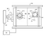
- FIG. 1schematically depicts a lithographic apparatus according to one embodiment of the invention.
- the apparatuscomprises:
- an illumination system (illuminator) ILconfigured to condition a radiation beam PB (e.g. UV radiation or DUV radiation).
- PBe.g. UV radiation or DUV radiation
- a support structuree.g. a mask table
- MTconstructed to support a patterning device (e.g. a mask) MA and connected to a first positioner PM configured to accurately position the patterning device in accordance with certain parameters;
- a substrate tablee.g. a wafer table
- WTconstructed to hold a substrate (e.g. a resist-coated wafer) W and connected to a second positioner PW configured to accurately position the substrate in accordance with certain parameters
- a projection systeme.g. a refractive projection lens system
- PLconfigured to project a pattern imparted to the radiation beam PB by patterning device MA onto a target portion C (e.g. comprising one or more dies) of the substrate W.
- the illumination systemmay include various types of optical components, such as refractive, reflective, magnetic, electromagnetic, electrostatic or other types of optical components, or any combination thereof, for directing, shaping, or controlling radiation.
- optical componentssuch as refractive, reflective, magnetic, electromagnetic, electrostatic or other types of optical components, or any combination thereof, for directing, shaping, or controlling radiation.
- the support structureholds the patterning device in a manner that depends on the orientation of the patterning device, the design of the lithographic apparatus, and other conditions, such as for example whether or not the patterning device is held in a vacuum environment.
- the support structurecan use mechanical, vacuum, electrostatic or other clamping techniques to hold the patterning device.
- the support structuremay be a frame or a table, for example, which may be fixed or movable as required.
- the support structuremay ensure that the patterning device is at a desired position, for example with respect to the projection system. Any use of the terms “reticle” or “mask” herein may be considered synonymous with the more general term “patterning device”.
- patterning deviceused herein should be broadly interpreted as referring to any device that can be used to impart a radiation beam with a pattern in its cross-section such as to create a pattern in a target portion of the substrate. It should be noted that the pattern imparted to the radiation beam may not exactly correspond to the desired pattern in the target portion of the substrate, for example if the pattern includes phase-shifting features or so called assist features. Generally, the pattern imparted to the radiation beam will correspond to a particular functional layer in a device being created in the target portion, such as an integrated circuit.
- the patterning devicemay be transmissive or reflective.
- Examples of patterning devicesinclude masks, programmable mirror arrays, and programmable LCD panels.
- Masksare well known in lithography, and include mask types such as binary, alternating phase-shift, and attenuated phase-shift, as well as various hybrid mask types.
- An example of a programmable mirror arrayemploys a matrix arrangement of small mirrors, each of which can be individually tilted so as to reflect an incoming radiation beam in different directions. The tilted mirrors impart a pattern in a radiation beam which is reflected by the mirror matrix.
- projection systemused herein should be broadly interpreted as encompassing any type of projection system, including refractive, reflective, catadioptric, magnetic, electromagnetic and electrostatic optical systems, or any combination thereof, as appropriate for the exposure radiation being used, or for other factors such as the use of an immersion liquid or the use of a vacuum. Any use of the term “projection lens” herein may be considered as synonymous with the more general term “projection system”.
- the apparatusis of a transmissive type (e.g. employing a transmissive mask).
- the apparatusmay be of a reflective type (e.g. employing a programmable mirror array of a type as referred to above, or employing a reflective mask).
- the lithographic apparatusmay be of a type having two (dual stage) or more substrate tables (and/or two or more support structures).
- the additional tablesmay be used in parallel, or preparatory steps may be carried out on one or more tables while one or more other tables are being used for exposure.
- the illuminator ILreceives a radiation beam from a radiation source 50.
- the source and the lithographic apparatusmay be separate entities, for example when the source is an excimer laser. In such cases, the source is not considered to form part of the lithographic apparatus and the radiation beam is passed from the source 50 to the illuminator IL with the aid of a beam delivery system BD comprising, for example, suitable directing mirrors and/or a beam expander. In other cases the source may be an integral part of the lithographic apparatus, for example when the source is a mercury lamp.
- the source 50 and the illuminator IL, together with the beam delivery system BD if required,may be referred to as a radiation system.
- the illuminator ILmay comprise an adjuster AD for adjusting the angular intensity distribution of the radiation beam.
- an adjuster ADfor adjusting the angular intensity distribution of the radiation beam.
- the illuminator ILmay comprise various other components, such as an integrator IN and a condenser CO.
- the illuminatormay be used to condition the radiation beam, to have a desired uniformity and intensity distribution in its cross-section.
- the radiation beam PBis incident on the patterning device (e.g., mask MA), which is held on the support structure (e.g., mask table MT), and is patterned by the patterning device. Having traversed the patterning device MA, the radiation beam PB passes through the projection system PL, which focuses the beam onto a target portion C of the substrate W.
- the substrate table WTcan be moved accurately, e.g. so as to position different target portions C in the path of the radiation beam PB.
- the first positioner PM and another position sensor(which is not explicitly depicted in FIG.
- the support structure MTcan be used to accurately position the patterning device MA with respect to the path of the radiation beam PB, e.g. after mechanical retrieval from a mask library, or during a scan.
- movement of the support structure MTmay be realized with the aid of a long-stroke module (coarse positioning) and a short-stroke module (fine positioning), which form part of the first positioner PM.
- movement of the substrate table WTmay be realized using a long-stroke module and a short-stroke module, which form part of the second positioner PW.
- the support structure MTmay be connected to a short-stroke actuator only, or may be fixed.
- Patterning device MA and substrate Wmay be aligned using patterning device alignment marks M 1 , M 2 and substrate alignment marks P 1 , P 2 .
- the substrate alignment marks as illustratedoccupy dedicated target portions, they may be located in spaces between target portions (these are known as scribe-lane alignment marks).
- the patterning device alignment marksmay be located between the dies.
- the depicted apparatuscould be used in at least one of the following modes:
- step modethe support structure MT and the substrate table WT are kept essentially stationary, while an entire pattern imparted to the radiation beam is projected onto a target portion C at one time (i.e. a single static exposure).
- the substrate table WTis then shifted in the X and/or Y direction so that a different target portion C can be exposed.
- step modethe maximum size of the exposure field limits the size of the target portion C imaged in a single static exposure.
- the support structure MT and the substrate table WTare scanned synchronously while a pattern imparted to the radiation beam is projected onto a target portion C (i.e. a single dynamic exposure).
- the velocity and direction of the substrate table WT relative to the support structure MTmay be determined by the (de-)magnification and image reversal characteristics of the projection system PL.
- the maximum size of the exposure fieldlimits the width (in the non-scanning direction) of the target portion in a single dynamic exposure, whereas the length of the scanning motion determines the height (in the scanning direction) of the target portion.
- the support structure MTis kept essentially stationary holding a programmable patterning device, and the substrate table WT is moved or scanned while a pattern imparted to the radiation beam is projected onto a target portion C.
- a pulsed radiation sourceis employed and the programmable patterning device is updated as required after each movement of the substrate table WT or in between successive radiation pulses during a scan.
- This mode of operationcan be readily applied to maskless lithography that utilizes programmable patterning device, such as a programmable mirror array of a type as referred to above.
- FIG. 4A further immersion lithography solution with a localized liquid supply system is shown in FIG. 4 .
- Liquidis supplied by two groove inlets IN on either side of the projection system PL and is removed by a plurality of discrete outlets OUT arranged radially outwardly of the inlets IN.
- the inlets IN and OUTcan be arranged in a plate with a hole in its center and through which the projection beam is projected.
- Liquidis supplied by one groove inlet IN on one side of the projection system PL and removed by a plurality of discrete outlets OUT on the other side of the projection system PL, causing a flow of a thin film of liquid between the projection system PL and the substrate W.
- the choice of which combination of inlet IN and outlets OUT to usecan depend on the direction of movement of the substrate W (the other combination of inlet IN and outlets OUT being inactive).
- Another immersion lithography solution with a localized liquid supply system solutionwhich has been proposed is to provide the liquid supply system with a liquid confinement structure which extends along at least a part of a boundary of the space between the final element of the projection system and the substrate table.
- the liquid confinement structureis substantially stationary relative to the projection system in the XY plane though there may be some relative movement in the Z direction (in the direction of the optical axis).
- a sealis formed between the liquid confinement structure and the surface of the substrate.
- the sealis a contactless seal such as a gas seal.
- FIG. 5shows a liquid supply system comprising a liquid confinement structure (sometimes referred to as an immersion hood or showerhead) according to an embodiment of the invention.
- a liquid confinement structuresometimes referred to as an immersion hood or showerhead
- FIG. 5depicts an arrangement of a reservoir 10 , which forms a contactless seal to the substrate around the image field of the projection system so that liquid is confined to fill a space between the substrate surface and the final element of the projection system.
- a liquid confinement structure 12 positioned below and surrounding the final element of the projection system PLforms the reservoir. Liquid is brought into the space below the projection system and within the liquid confinement structure 12 .
- the liquid confinement structure 12extends a little above the final element of the projection system and the liquid level rises above the final element so that a buffer of liquid is provided.
- the liquid confinement structure 12has an inner periphery that at the upper end preferably closely conforms to the shape of the projection system or the final element thereof and may, e.g., be round. At the bottom, the inner periphery closely conforms to the shape of the image field, e.g., rectangular though this need not be the case.
- the liquidis confined in the reservoir by a gas seal 16 between the bottom of the liquid confinement structure 12 and the surface of the substrate W.
- the gas sealis formed by gas, e.g. air, synthetic air, N 2 or an inert gas, provided under pressure via inlet 15 to the gap between liquid confinement structure 12 and substrate and extracted via outlet 14 .
- gase.g. air, synthetic air, N 2 or an inert gas
- the overpressure on the gas inlet 15 , vacuum level on the outlet 14 and geometry of the gapare arranged so that there is a high-velocity gas flow inwards that confines the liquid.
- other types of sealcould be used to contain the liquid such as simply an outlet to remove liquid and/or gas.
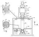
- FIG. 6shows substrate stage arrangements according to an embodiment of the invention.
- the embodimentis a so-called dual stage apparatus in which at substrate level there are two stations: an exposure station ES and a measurement station MS.
- an exposure station ESAt the exposure station, substrates are exposed while at the measurement station various measurements are carried out, for example, to characterize a substrate prior to exposure or to verify that exposure has been carried out correctly.
- One or more sensorsmay be provided at the measurement station to perform the measurements and examples of the types of a sensor that may be provided at the measurement station include a level sensor LS to make a height map of a substrate prior to exposure, an alignment sensor AS to measure the position of one or more alignment markers on the substrate, and a scatterometer SM to examine the latent image of an exposed substrate.
- a load/unload robot(not shown) is also provided to load and unload substrates to a substrate table at the measurement station.
- a dual stage apparatuswhile one substrate is being exposed, a previously exposed substrate can be measured and/or a next substrate to be exposed can be pre-measured.
- a dual stage apparatustherefore can have improved throughput as compared to a single stage apparatus in which both measurement and exposure steps are carried out at a single station.
- the apparatushas two substrate tables WT 1 , WT 2 which are positioned by a positioning system PW comprising two H-drives, each to position a substrate table within one of the stations.
- a positioning system PWcomprising two H-drives, each to position a substrate table within one of the stations.
- FIG. 7at the end of an exposure process, the two substrate tables WT 1 , WT 2 are positioned at the boundary between the two stations and decoupled from the positioning system PW; each H-drive then pick-ups the substrate table released by the other H-drive. This procedure is sometimes referred to as a chuck swap or table exchange.
- the substrate W 2 that has just been pre-measured at the measurement stationcan be exposed at the exposure station and the substrate W 1 that has just been exposed can be measured and/or unloaded at the measurement station.
- An alternative arrangementhas two measurement stations and two substrate tables but a single exposure station. Each substrate table is positioned by a drive system having a range including its own measurement station and the exposure station so that there is no exchange of tables between parts of the positioning system. However, there is still a period which may be referred to as table exchange during which one table is moving out of the exposure station and the other one is moving in.
- a closing platemay be provided in a recess on the substrate table from which it is picked up by a liquid confinement structure IH before the substrate table is moved out from under the projection system PL.
- a third table 21is provided, with a positioning system 22 , 23 that is capable of positioning the third table under the projection system PL and liquid confinement structure IH.
- the third table 21 and the positioning system 22 , 23may together form the third stage 20 .
- the third table 21may fulfill at least two functions. Firstly, it can provide a confining surface at the bottom of the liquid confinement structure IH when the substrate table WT 1 , WT 2 is removed to prevent the immersion liquid leaking out into the remainder of the apparatus.
- the third table 21may comprise a sensor unit 24 comprising one or more sensors to make a measurement of the aerial image projected by the projection system PL.
- the sensor unit 24may advantageously include a shearing interferometer sensor, which is used to characterize aberrations in the projection system PL, since the measurements taken by such a sensor take a comparatively long time and are important to imaging performance.
- the sensor(s)can therefore be used to make a measurement at substrate level without reducing throughput by making use of the substrate table exchange interval.
- the reduction in downtime achievablemay therefore be substantial.
- the desired measurement(s)e.g., measurements necessary for a calibration
- the measurement(s)may be split into several parts and performed during several substrate table exchange periods, possibly with modifications to account for factors that may change over the period between measurements.
- the exchange periodmay be extended to accommodate the measurement(s) on one or more occasions causing some loss of throughput, but less than if the whole measurement were carried out during a substrate exposure downtime.
- An advantagealso accrues from providing a polarization sensor as part of the sensor unit on the third table as a polarization sensor can be quite bulky, involving several optical components, and therefore may be difficult to accommodate on one or both of the substrate tables WT 1 , WT 2 .
- the positioning system 22 , 23may comprise simply a long stroke drive module to position the third table 21 under the projection system PL, as shown in FIG. 7 , in synchronism, for example, with the removal of the substrate table WT 1 , WT 2 .
- Thismay be carried out under control of a controller CS connected to the positioning system of the third table 21 and the positioning system of the substrate table WT 1 , WT 2 .
- a short stroke drive modulemay be included if the sensor requires more accurate positioning and/or scanning to make the measurement.
- the sensorsmay be fitted into the area of the exposure field so as to operate simultaneously or if that is inconvenient, the positioning system may be arranged to position different sensors in the exposure field successively.
- the third tablemay also be provided with other devices, e.g. a cleaning device configured to cleaning a final element of the projection system, in addition to or instead of the sensor.
- the cleaning devicemay use gas, electric particles, a laser or other mechanisms for cleaning the projection system.
- a third tablemay also be used in an immersion lithography apparatus without a sensor or other device and rather simply to provide a confining surface for the liquid supply system during, for example, table exchange and/or substrate loading and unloading.
- a multiple (e.g., two) stage lithographic apparatusmay comprise one exposure station and more than one measurement station.
- a measurement stationmay be provided on opposite sides of an exposure station, where the projection system is positioned, and then two substrate tables may be shuttled between the two measurement stations and the exposure station.
- a first substrate tablemay be shuttled between the exposure station and a first measurement station and the second substrate table may be shuttled between the exposure station and a second measurement station.
- the two substrate tablesmay be shuttled in tandem back and forth so that the first substrate table only moves between the exposure station and a first measurement station and the second substrate table moves only between the exposure station and a second measurement station.
- lithographic apparatusin the manufacture of ICs
- the lithographic apparatus described hereinmay have other applications, such as the manufacture of integrated optical systems, guidance and detection patterns for magnetic domain memories, flat-panel displays, liquid-crystal displays (LCDs), thin-film magnetic heads, etc.
- LCDsliquid-crystal displays
- any use of the terms “wafer” or “die” hereinmay be considered as synonymous with the more general terms “substrate” or “target portion”, respectively.
- the substrate referred to hereinmay be processed, before or after exposure, in for example a track (a tool that typically applies a layer of resist to a substrate and develops the exposed resist), a metrology tool and/or an inspection tool. Where applicable, the disclosure herein may be applied to such and other substrate processing tools. Further, the substrate may be processed more than once, for example in order to create a multi-layer IC, so that the term substrate used herein may also refer to a substrate that already contains multiple processed layers.
- UV radiatione.g. having a wavelength of or about 365, 248, 193, 157 or 126 nm.
- lensmay refer to any one or combination of various types of optical components, including refractive and reflective optical components.
- the inventionmay take the form of a computer program containing one or more sequences of machine-readable instructions describing a method as disclosed above, or a data storage medium (e.g. semiconductor memory, magnetic or optical disk) having such a computer program stored therein.
- a data storage mediume.g. semiconductor memory, magnetic or optical disk
- a liquid supply systemis any mechanism that provides a liquid to a space between the projection system and the substrate and/or substrate table. It may comprise any combination of one or more structures, one or more liquid inlets, one or more gas inlets, one or more gas outlets, and/or one or more liquid outlets, the combination providing and confining the liquid to the space.
- a surface of the spacemay be limited to a portion of the substrate and/or substrate table, a surface of the space may completely cover a surface of the substrate and/or substrate table, or the space may envelop the substrate and/or substrate table.
Landscapes
- Physics & Mathematics (AREA)
- General Physics & Mathematics (AREA)
- Health & Medical Sciences (AREA)
- Life Sciences & Earth Sciences (AREA)
- Atmospheric Sciences (AREA)
- Toxicology (AREA)
- Engineering & Computer Science (AREA)
- Environmental & Geological Engineering (AREA)
- Epidemiology (AREA)
- Public Health (AREA)
- Exposure And Positioning Against Photoresist Photosensitive Materials (AREA)
- Exposure Of Semiconductors, Excluding Electron Or Ion Beam Exposure (AREA)
- Container, Conveyance, Adherence, Positioning, Of Wafer (AREA)
- Length Measuring Devices By Optical Means (AREA)
Abstract
Description
Claims (38)
Priority Applications (7)
| Application Number | Priority Date | Filing Date | Title |
|---|---|---|---|
| US12/327,414US8233137B2 (en) | 2004-12-20 | 2008-12-03 | Lithographic apparatus and device manufacturing method |
| US13/188,096US9116443B2 (en) | 2004-12-20 | 2011-07-21 | Lithographic apparatus and device manufacturing method |
| US13/189,212US8462312B2 (en) | 2004-12-20 | 2011-07-22 | Lithographic apparatus and device manufacturing method |
| US14/500,386US9329494B2 (en) | 2004-12-20 | 2014-09-29 | Lithographic apparatus |
| US14/661,929US9417535B2 (en) | 2004-12-20 | 2015-03-18 | Lithographic apparatus |
| US15/216,670US9835960B2 (en) | 2004-12-20 | 2016-07-21 | Lithographic apparatus |
| US15/802,429US10248035B2 (en) | 2004-12-20 | 2017-11-02 | Lithographic apparatus |
Applications Claiming Priority (2)
| Application Number | Priority Date | Filing Date | Title |
|---|---|---|---|
| US11/015,766US7528931B2 (en) | 2004-12-20 | 2004-12-20 | Lithographic apparatus and device manufacturing method |
| US12/327,414US8233137B2 (en) | 2004-12-20 | 2008-12-03 | Lithographic apparatus and device manufacturing method |
Related Parent Applications (1)
| Application Number | Title | Priority Date | Filing Date |
|---|---|---|---|
| US11/015,766ContinuationUS7528931B2 (en) | 2004-12-20 | 2004-12-20 | Lithographic apparatus and device manufacturing method |
Related Child Applications (1)
| Application Number | Title | Priority Date | Filing Date |
|---|---|---|---|
| US13/188,096ContinuationUS9116443B2 (en) | 2004-12-20 | 2011-07-21 | Lithographic apparatus and device manufacturing method |
Publications (2)
| Publication Number | Publication Date |
|---|---|
| US20090079951A1 US20090079951A1 (en) | 2009-03-26 |
| US8233137B2true US8233137B2 (en) | 2012-07-31 |
Family
ID=36595233
Family Applications (8)
| Application Number | Title | Priority Date | Filing Date |
|---|---|---|---|
| US11/015,766Expired - Fee RelatedUS7528931B2 (en) | 2004-12-20 | 2004-12-20 | Lithographic apparatus and device manufacturing method |
| US12/327,414Expired - Fee RelatedUS8233137B2 (en) | 2004-12-20 | 2008-12-03 | Lithographic apparatus and device manufacturing method |
| US13/188,096Active2027-01-02US9116443B2 (en) | 2004-12-20 | 2011-07-21 | Lithographic apparatus and device manufacturing method |
| US13/189,212Expired - Fee RelatedUS8462312B2 (en) | 2004-12-20 | 2011-07-22 | Lithographic apparatus and device manufacturing method |
| US14/500,386Expired - Fee RelatedUS9329494B2 (en) | 2004-12-20 | 2014-09-29 | Lithographic apparatus |
| US14/661,929Expired - Fee RelatedUS9417535B2 (en) | 2004-12-20 | 2015-03-18 | Lithographic apparatus |
| US15/216,670Expired - Fee RelatedUS9835960B2 (en) | 2004-12-20 | 2016-07-21 | Lithographic apparatus |
| US15/802,429Expired - Fee RelatedUS10248035B2 (en) | 2004-12-20 | 2017-11-02 | Lithographic apparatus |
Family Applications Before (1)
| Application Number | Title | Priority Date | Filing Date |
|---|---|---|---|
| US11/015,766Expired - Fee RelatedUS7528931B2 (en) | 2004-12-20 | 2004-12-20 | Lithographic apparatus and device manufacturing method |
Family Applications After (6)
| Application Number | Title | Priority Date | Filing Date |
|---|---|---|---|
| US13/188,096Active2027-01-02US9116443B2 (en) | 2004-12-20 | 2011-07-21 | Lithographic apparatus and device manufacturing method |
| US13/189,212Expired - Fee RelatedUS8462312B2 (en) | 2004-12-20 | 2011-07-22 | Lithographic apparatus and device manufacturing method |
| US14/500,386Expired - Fee RelatedUS9329494B2 (en) | 2004-12-20 | 2014-09-29 | Lithographic apparatus |
| US14/661,929Expired - Fee RelatedUS9417535B2 (en) | 2004-12-20 | 2015-03-18 | Lithographic apparatus |
| US15/216,670Expired - Fee RelatedUS9835960B2 (en) | 2004-12-20 | 2016-07-21 | Lithographic apparatus |
| US15/802,429Expired - Fee RelatedUS10248035B2 (en) | 2004-12-20 | 2017-11-02 | Lithographic apparatus |
Country Status (2)
| Country | Link |
|---|---|
| US (8) | US7528931B2 (en) |
| JP (10) | JP2006179906A (en) |
Cited By (4)
| Publication number | Priority date | Publication date | Assignee | Title |
|---|---|---|---|---|
| US20070195300A1 (en)* | 2003-04-11 | 2007-08-23 | Nikon Corporation | Apparatus and method for maintaining immersion fluid in the gap under the projection lens during wafer exchange in an immersion lithography machine |
| US20100182584A1 (en)* | 2004-02-02 | 2010-07-22 | Nikon Corporation | Stage drive method and stage unit, exposure apparatus, and device manufacturing method |
| US20110025997A1 (en)* | 2003-06-19 | 2011-02-03 | Nikon Corporation | Exposure apparatus, and device manufacturing method |
| US20110279806A1 (en)* | 2004-12-20 | 2011-11-17 | Asml Netherlands B.V. | Lithographic apparatus and device manufacturing method |
Families Citing this family (33)
| Publication number | Priority date | Publication date | Assignee | Title |
|---|---|---|---|---|
| US7436484B2 (en)* | 2004-12-28 | 2008-10-14 | Asml Netherlands B.V. | Lithographic apparatus and device manufacturing method |
| US8547522B2 (en)* | 2005-03-03 | 2013-10-01 | Asml Netherlands B.V. | Dedicated metrology stage for lithography applications |
| US20060219947A1 (en)* | 2005-03-03 | 2006-10-05 | Asml Netherlands B.V. | Dedicated metrology stage for lithography applications |
| USRE43576E1 (en) | 2005-04-08 | 2012-08-14 | Asml Netherlands B.V. | Dual stage lithographic apparatus and device manufacturing method |
| KR101344142B1 (en) | 2005-04-25 | 2013-12-23 | 가부시키가이샤 니콘 | Exposure method, exposure apparatus and device manufacturing method |
| KR20080031376A (en)* | 2005-07-11 | 2008-04-08 | 가부시키가이샤 니콘 | Exposure apparatus and device manufacturing method |
| EP1918983A4 (en)* | 2005-08-05 | 2010-03-31 | Nikon Corp | Stage apparatus and exposure apparatus |
| WO2007029829A1 (en)* | 2005-09-09 | 2007-03-15 | Nikon Corporation | Exposure apparatus, exposure method, and device production method |
| US8675171B2 (en)* | 2006-08-31 | 2014-03-18 | Nikon Corporation | Movable body drive system and movable body drive method, pattern formation apparatus and method, exposure apparatus and method, device manufacturing method, and decision-making method |
| KR101444473B1 (en)* | 2006-08-31 | 2014-09-24 | 가부시키가이샤 니콘 | Moving body driving method and moving body driving system, pattern forming method and apparatus, exposure method and apparatus, and device manufacturing method |
| CN102360169B (en)* | 2006-09-01 | 2014-01-22 | 株式会社尼康 | Movable body drive method and movable body drive system, pattern formation method and apparatus, exposure method and apparatus, device manufacturing method, and calibration method |
| US7872730B2 (en)* | 2006-09-15 | 2011-01-18 | Nikon Corporation | Immersion exposure apparatus and immersion exposure method, and device manufacturing method |
| KR100781971B1 (en) | 2006-11-28 | 2007-12-06 | 삼성전자주식회사 | Wafer stage module of twin scan exposure equipment and its control method |
| US7599064B2 (en)* | 2007-03-07 | 2009-10-06 | Asml Netherlands B.V. | Inspection method and apparatus, lithographic apparatus, lithographic processing cell and device manufacturing method, substrate for use in the methods |
| US8237911B2 (en) | 2007-03-15 | 2012-08-07 | Nikon Corporation | Apparatus and methods for keeping immersion fluid adjacent to an optical assembly during wafer exchange in an immersion lithography machine |
| US7911612B2 (en)* | 2007-06-13 | 2011-03-22 | Asml Netherlands B.V. | Inspection method and apparatus, lithographic apparatus, lithographic processing cell and device manufacturing method |
| US7586108B2 (en)* | 2007-06-25 | 2009-09-08 | Asml Netherlands B.V. | Radiation detector, method of manufacturing a radiation detector and lithographic apparatus comprising a radiation detector |
| TWI450047B (en) | 2007-07-13 | 2014-08-21 | Mapper Lithography Ip Bv | Lithography ststem, method of clamping and wafer table |
| US8705010B2 (en) | 2007-07-13 | 2014-04-22 | Mapper Lithography Ip B.V. | Lithography system, method of clamping and wafer table |
| US8896809B2 (en)* | 2007-08-15 | 2014-11-25 | Asml Netherlands B.V. | Lithographic apparatus and device manufacturing method |
| NL1036180A1 (en)* | 2007-11-20 | 2009-05-25 | Asml Netherlands Bv | Stage system, lithographic apparatus including such stage system, and correction method. |
| US9176393B2 (en) | 2008-05-28 | 2015-11-03 | Asml Netherlands B.V. | Lithographic apparatus and a method of operating the apparatus |
| JP5199982B2 (en)* | 2008-12-08 | 2013-05-15 | エーエスエムエル ネザーランズ ビー.ブイ. | Lithographic apparatus |
| TWI526787B (en)* | 2009-05-15 | 2016-03-21 | 尼康股份有限公司 | A moving body device, a power transmission device, and an exposure device, and a device manufacturing method |
| TWI408331B (en)* | 2009-12-17 | 2013-09-11 | Ind Tech Res Inst | Measurement device and method of double-sided optical films |
| CN102193323B (en)* | 2010-03-05 | 2013-04-10 | 上海微电子装备有限公司 | Double-stage system of lithography machine |
| EP2469339B1 (en)* | 2010-12-21 | 2017-08-30 | ASML Netherlands B.V. | Lithographic apparatus and device manufacturing method |
| US9207549B2 (en) | 2011-12-29 | 2015-12-08 | Nikon Corporation | Exposure apparatus and exposure method, and device manufacturing method with encoder of higher reliability for position measurement |
| US9772564B2 (en) | 2012-11-12 | 2017-09-26 | Nikon Corporation | Exposure apparatus and exposure method, and device manufacturing method |
| JP6362312B2 (en)* | 2013-09-09 | 2018-07-25 | キヤノン株式会社 | Exposure apparatus and device manufacturing method using the same |
| WO2017084797A1 (en)* | 2015-11-20 | 2017-05-26 | Asml Netherlands B.V. | Lithographic apparatus and method of operating a lithographic apparatus |
| SG11201906413XA (en)* | 2017-02-03 | 2019-08-27 | Asml Netherlands Bv | Exposure apparatus |
| JP7212528B2 (en)* | 2019-01-17 | 2023-01-25 | キヤノン株式会社 | Lithographic apparatus, metrology methods, and methods of manufacturing articles |
Citations (104)
| Publication number | Priority date | Publication date | Assignee | Title |
|---|---|---|---|---|
| US3573975A (en) | 1968-07-10 | 1971-04-06 | Ibm | Photochemical fabrication process |
| US3648587A (en) | 1967-10-20 | 1972-03-14 | Eastman Kodak Co | Focus control for optical instruments |
| EP0023231A1 (en) | 1979-07-27 | 1981-02-04 | Tabarelli, Werner, Dr. | Optical lithographic method and apparatus for copying a pattern onto a semiconductor wafer |
| FR2474708A1 (en) | 1980-01-24 | 1981-07-31 | Dme | Micro:photo:lithographic process giving high line resolution - with application of immersion oil between mask and photosensitive layer before exposure |
| US4346164A (en) | 1980-10-06 | 1982-08-24 | Werner Tabarelli | Photolithographic method for the manufacture of integrated circuits |
| US4390273A (en) | 1981-02-17 | 1983-06-28 | Censor Patent-Und Versuchsanstalt | Projection mask as well as a method and apparatus for the embedding thereof and projection printing system |
| US4396705A (en) | 1980-09-19 | 1983-08-02 | Hitachi, Ltd. | Pattern forming method and pattern forming apparatus using exposures in a liquid |
| JPS58202448A (en) | 1982-05-21 | 1983-11-25 | Hitachi Ltd | exposure equipment |
| DD206607A1 (en) | 1982-06-16 | 1984-02-01 | Mikroelektronik Zt Forsch Tech | METHOD AND DEVICE FOR ELIMINATING INTERFERENCE EFFECTS |
| US4480910A (en) | 1981-03-18 | 1984-11-06 | Hitachi, Ltd. | Pattern forming apparatus |
| US4509852A (en) | 1980-10-06 | 1985-04-09 | Werner Tabarelli | Apparatus for the photolithographic manufacture of integrated circuit elements |
| DD221563A1 (en) | 1983-09-14 | 1985-04-24 | Mikroelektronik Zt Forsch Tech | IMMERSIONS OBJECTIVE FOR THE STEP-BY-STEP PROJECTION IMAGING OF A MASK STRUCTURE |
| DD224448A1 (en) | 1984-03-01 | 1985-07-03 | Zeiss Jena Veb Carl | DEVICE FOR PHOTOLITHOGRAPHIC STRUCTURAL TRANSMISSION |
| JPS61109053A (en) | 1984-11-01 | 1986-05-27 | Nippon Kogaku Kk <Nikon> | Projection optical device |
| DD242880A1 (en) | 1983-01-31 | 1987-02-11 | Kuch Karl Heinz | DEVICE FOR PHOTOLITHOGRAPHIC STRUCTURAL TRANSMISSION |
| JPS6265326A (en) | 1985-09-18 | 1987-03-24 | Hitachi Ltd | Exposure device |
| JPS62121417A (en) | 1985-11-22 | 1987-06-02 | Hitachi Ltd | Immersion objective lens device |
| JPS63157419A (en) | 1986-12-22 | 1988-06-30 | Toshiba Corp | Fine pattern transfer apparatus |
| EP0418427A2 (en) | 1989-09-06 | 1991-03-27 | Eiichi Miyake | Exposure process |
| US5040020A (en) | 1988-03-31 | 1991-08-13 | Cornell Research Foundation, Inc. | Self-aligned, high resolution resonant dielectric lithography |
| US5121256A (en) | 1991-03-14 | 1992-06-09 | The Board Of Trustees Of The Leland Stanford Junior University | Lithography system employing a solid immersion lens |
| JPH04305917A (en) | 1991-04-02 | 1992-10-28 | Nikon Corp | Close-contact exposure equipment |
| JPH04305915A (en) | 1991-04-02 | 1992-10-28 | Nikon Corp | Adhesion type exposure device |
| JPH06124873A (en) | 1992-10-09 | 1994-05-06 | Canon Inc | Immersion projection exposure system |
| JPH07132262A (en) | 1992-12-21 | 1995-05-23 | Tokyo Electron Ltd | Liquid treating device of immersion type |
| JPH07220990A (en) | 1994-01-28 | 1995-08-18 | Hitachi Ltd | Pattern forming method and exposure apparatus thereof |
| US5610683A (en) | 1992-11-27 | 1997-03-11 | Canon Kabushiki Kaisha | Immersion type projection exposure apparatus |
| US5650840A (en)* | 1994-09-13 | 1997-07-22 | Nikon Corporation | Focus detecting method and apparatus |
| JPH10228661A (en) | 1997-02-14 | 1998-08-25 | Sony Corp | Master disk manufacturing aligner for optical recording medium |
| JPH10255319A (en) | 1997-03-12 | 1998-09-25 | Hitachi Maxell Ltd | Master exposure apparatus and method |
| US5825043A (en) | 1996-10-07 | 1998-10-20 | Nikon Precision Inc. | Focusing and tilting adjustment system for lithography aligner, manufacturing apparatus or inspection apparatus |
| JPH10303114A (en) | 1997-04-23 | 1998-11-13 | Nikon Corp | Immersion type exposure equipment |
| JPH10340846A (en) | 1997-06-10 | 1998-12-22 | Nikon Corp | Aligner, its manufacture, exposing method and device manufacturing method |
| US5900354A (en) | 1997-07-03 | 1999-05-04 | Batchelder; John Samuel | Method for optical inspection and lithography |
| WO1999023692A1 (en) | 1997-10-31 | 1999-05-14 | Nikon Corporation | Aligner and exposure method |
| JPH11162831A (en) | 1997-11-21 | 1999-06-18 | Nikon Corp | Projection exposure apparatus and projection exposure method |
| JPH11176727A (en) | 1997-12-11 | 1999-07-02 | Nikon Corp | Projection exposure equipment |
| WO1999049504A1 (en) | 1998-03-26 | 1999-09-30 | Nikon Corporation | Projection exposure method and system |
| JPH11283903A (en) | 1998-03-30 | 1999-10-15 | Nikon Corp | Projection optical system inspection apparatus and projection exposure apparatus having the same |
| JP2000058436A (en) | 1998-08-11 | 2000-02-25 | Nikon Corp | Projection exposure apparatus and exposure method |
| JP2000091270A (en) | 1998-09-16 | 2000-03-31 | Nec Corp | Sputter growth method for electrodes used in ferroelectric capacitors |
| EP1039511A1 (en) | 1997-12-12 | 2000-09-27 | Nikon Corporation | Projection exposure method and projection aligner |
| JP2001091849A (en) | 1999-09-21 | 2001-04-06 | Olympus Optical Co Ltd | Immersion objective lens for microscope |
| US6236634B1 (en) | 1996-08-26 | 2001-05-22 | Digital Papyrus Corporation | Method and apparatus for coupling an optical lens to a disk through a coupling medium having a relatively high index of refraction |
| US20020020821A1 (en) | 2000-08-08 | 2002-02-21 | Koninklijke Philips Electronics N.V. | Method of manufacturing an optically scannable information carrier |
| US20020163629A1 (en) | 2001-05-07 | 2002-11-07 | Michael Switkes | Methods and apparatus employing an index matching medium |
| US6496257B1 (en) | 1997-11-21 | 2002-12-17 | Nikon Corporation | Projection exposure apparatus and method |
| US20030123040A1 (en) | 2001-11-07 | 2003-07-03 | Gilad Almogy | Optical spot grid array printer |
| US6600547B2 (en) | 2001-09-24 | 2003-07-29 | Nikon Corporation | Sliding seal |
| US6603130B1 (en) | 1999-04-19 | 2003-08-05 | Asml Netherlands B.V. | Gas bearings for use with vacuum chambers and their application in lithographic projection apparatuses |
| US20040000627A1 (en) | 2002-06-28 | 2004-01-01 | Carl Zeiss Semiconductor Manufacturing Technologies Ag | Method for focus detection and an imaging system with a focus-detection system |
| US20040075895A1 (en) | 2002-10-22 | 2004-04-22 | Taiwan Semiconductor Manufacturing Co., Ltd. | Apparatus for method for immersion lithography |
| US20040114117A1 (en) | 2002-11-18 | 2004-06-17 | Asml Netherlands B.V. | Lithographic apparatus and device manufacturing method |
| WO2004053955A1 (en) | 2002-12-10 | 2004-06-24 | Nikon Corporation | Exposure system and device producing method |
| WO2004053957A1 (en) | 2002-12-10 | 2004-06-24 | Nikon Corporation | Surface position detection apparatus, exposure method, and device porducing method |
| WO2004053958A1 (en) | 2002-12-10 | 2004-06-24 | Nikon Corporation | Exposure apparatus and method for manufacturing device |
| WO2004053596A2 (en) | 2002-12-10 | 2004-06-24 | Carl Zeiss Smt Ag | Method for adjusting a desired optical property of a positioning lens and microlithographic projection exposure system |
| WO2004053951A1 (en) | 2002-12-10 | 2004-06-24 | Nikon Corporation | Exposure method, exposure apparatus and method for manufacturing device |
| WO2004053956A1 (en) | 2002-12-10 | 2004-06-24 | Nikon Corporation | Exposure apparatus, exposure method and method for manufacturing device |
| WO2004053954A1 (en) | 2002-12-10 | 2004-06-24 | Nikon Corporation | Exposure apparatus and method for manufacturing device |
| WO2004053952A1 (en) | 2002-12-10 | 2004-06-24 | Nikon Corporation | Exposure apparatus and method for manufacturing device |
| WO2004053959A1 (en) | 2002-12-10 | 2004-06-24 | Nikon Corporation | Optical device and projection exposure apparatus using such optical device |
| WO2004053950A1 (en) | 2002-12-10 | 2004-06-24 | Nikon Corporation | Exposure apparatus and method for manufacturing device |
| WO2004053953A1 (en) | 2002-12-10 | 2004-06-24 | Nikon Corporation | Exposure apparatus and method for manufacturing device |
| WO2004055803A1 (en) | 2002-12-13 | 2004-07-01 | Koninklijke Philips Electronics N.V. | Liquid removal in a method and device for irradiating spots on a layer |
| WO2004057590A1 (en) | 2002-12-19 | 2004-07-08 | Koninklijke Philips Electronics N.V. | Method and device for irradiating spots on a layer |
| WO2004057589A1 (en) | 2002-12-19 | 2004-07-08 | Koninklijke Philips Electronics N.V. | Method and device for irradiating spots on a layer |
| JP2004193252A (en) | 2002-12-10 | 2004-07-08 | Nikon Corp | Exposure method and device manufacturing method |
| US20040136494A1 (en) | 2002-11-12 | 2004-07-15 | Asml Netherlands B.V. | Lithographic apparatus and device manufacturing method |
| US20040160582A1 (en) | 2002-11-12 | 2004-08-19 | Asml Netherlands B.V. | Lithographic apparatus and device manufacturing method |
| US20040165159A1 (en) | 2002-11-12 | 2004-08-26 | Asml Netherlands B.V. | Lithographic apparatus and device manufacturing method |
| JP2004259966A (en) | 2003-02-26 | 2004-09-16 | Nikon Corp | Exposure apparatus and device manufacturing method |
| JP2004289128A (en) | 2002-11-12 | 2004-10-14 | Asml Netherlands Bv | Lithographic apparatus and device manufacturing method |
| JP2004289126A (en) | 2002-11-12 | 2004-10-14 | Asml Netherlands Bv | Lithography system and process for fabricating device |
| US20040227925A1 (en)* | 2003-04-18 | 2004-11-18 | Canon Kabushiki Kaisha | Exposure apparatus |
| WO2004104654A1 (en) | 2003-05-21 | 2004-12-02 | Nikon Corporation | Depolarization element, illumination optical device, exposure device, and exposure method |
| WO2004105107A1 (en) | 2003-05-23 | 2004-12-02 | Nikon Corporation | Exposure device and device manufacturing method |
| JP2004343114A (en) | 2003-05-13 | 2004-12-02 | Asml Netherlands Bv | Lithographic apparatus and method of manufacturing device |
| US20040239954A1 (en) | 2003-05-28 | 2004-12-02 | Joerg Bischoff | Resolution enhanced optical metrology |
| US20040263809A1 (en) | 2003-06-27 | 2004-12-30 | Canon Kabushiki Kaisha | Immersion exposure technique |
| US20050018155A1 (en) | 2003-06-27 | 2005-01-27 | Asml Netherlands B. V. | Lithographic apparatus and device manufacturing method |
| US20050024609A1 (en) | 2003-06-11 | 2005-02-03 | Asml Netherlands B.V. | Lithographic apparatus and device manufacturing method |
| US20050030497A1 (en) | 2003-06-25 | 2005-02-10 | Takashi Nakamura | Liquid immersion type exposure apparatus |
| US20050046934A1 (en) | 2003-08-29 | 2005-03-03 | Tokyo Electron Limited | Method and system for drying a substrate |
| US20050046813A1 (en) | 2003-07-16 | 2005-03-03 | Asmil Netherlands B.V. | Lithographic apparatus and device manufacturing method |
| US20050052632A1 (en) | 2003-09-09 | 2005-03-10 | Canon Kabushiki Kaisha | Exposure technique |
| US20050094125A1 (en) | 2003-10-31 | 2005-05-05 | Nikon Corporation | Supporting plate, stage device, exposure apparatus, and exposure method |
| US20050094116A1 (en) | 2003-08-29 | 2005-05-05 | Asml Netherlands B.V. | Gradient immersion lithography |
| US20050122505A1 (en) | 2003-12-08 | 2005-06-09 | Canon Kabushiki Kaisha | Substrate-holding technique |
| US20050134817A1 (en) | 2003-06-25 | 2005-06-23 | Takashi Nakamura | Liquid immersion type exposure apparatus |
| US20050132914A1 (en) | 2003-12-23 | 2005-06-23 | Asml Netherlands B.V. | Lithographic apparatus, alignment apparatus, device manufacturing method, and a method of converting an apparatus |
| US20050140948A1 (en) | 2003-12-26 | 2005-06-30 | Canon Kabushiki Kaisha | Exposure apparatus and method |
| US20050146694A1 (en) | 2004-01-07 | 2005-07-07 | Toshinobu Tokita | Exposure apparatus and device manufacturing method |
| US20050146693A1 (en) | 2003-12-09 | 2005-07-07 | Yoshinori Ohsaki | Exposure apparatus |
| US20050151942A1 (en) | 2003-12-26 | 2005-07-14 | Canon Kabushiki Kaisha | Exposure method and apparatus |
| US20050200815A1 (en) | 2004-02-09 | 2005-09-15 | Canon Kabushiki Kaisha | Projection exposure apparatus, device manufacturing method, and sensor unit |
| US20050213065A1 (en) | 2004-03-29 | 2005-09-29 | Atsushi Kitaoka | Exposure apparatus and method |
| US20050213066A1 (en) | 2004-03-29 | 2005-09-29 | Yuhei Sumiyoshi | Exposure apparatus |
| US20050219489A1 (en) | 2002-12-10 | 2005-10-06 | Nikon Corporation | Exposure apparatus and method for producing device |
| US20050233081A1 (en) | 2003-09-04 | 2005-10-20 | Toshinobu Tokita | Liquid immersion type exposure apparatus |
| JP2006074961A (en) | 2004-09-06 | 2006-03-16 | Nikon Corp | Linear motor, stage apparatus and exposure apparatus |
| US7327435B2 (en)* | 2003-04-11 | 2008-02-05 | Nikon Corporation | Apparatus and method for maintaining immersion fluid in the gap under the projection lens during wafer exchange in an immersion lithography machine |
| US7528931B2 (en)* | 2004-12-20 | 2009-05-05 | Asml Netherlands B.V. | Lithographic apparatus and device manufacturing method |
| US20100182584A1 (en) | 2004-02-02 | 2010-07-22 | Nikon Corporation | Stage drive method and stage unit, exposure apparatus, and device manufacturing method |
Family Cites Families (40)
| Publication number | Priority date | Publication date | Assignee | Title |
|---|---|---|---|---|
| DE221563C (en) | ||||
| DE224448C (en) | ||||
| DE206607C (en) | ||||
| DE242880C (en) | ||||
| JPS57117238A (en) | 1981-01-14 | 1982-07-21 | Nippon Kogaku Kk <Nikon> | Exposing and baking device for manufacturing integrated circuit with illuminometer |
| JPH0479212A (en)* | 1990-07-23 | 1992-03-12 | Canon Inc | semiconductor manufacturing equipment |
| US6078380A (en) | 1991-10-08 | 2000-06-20 | Nikon Corporation | Projection exposure apparatus and method involving variation and correction of light intensity distributions, detection and control of imaging characteristics, and control of exposure |
| US5631731A (en) | 1994-03-09 | 1997-05-20 | Nikon Precision, Inc. | Method and apparatus for aerial image analyzer |
| JP3632264B2 (en)* | 1995-11-30 | 2005-03-23 | 株式会社ニコン | X-ray projection exposure apparatus |
| DE69735016T2 (en)* | 1996-12-24 | 2006-08-17 | Asml Netherlands B.V. | Lithographic device with two object holders |
| JPH1116816A (en) | 1997-06-25 | 1999-01-22 | Nikon Corp | Projection exposure apparatus, exposure method using the apparatus, and method for manufacturing circuit device using the apparatus |
| US6897963B1 (en)* | 1997-12-18 | 2005-05-24 | Nikon Corporation | Stage device and exposure apparatus |
| JP4264676B2 (en)* | 1998-11-30 | 2009-05-20 | 株式会社ニコン | Exposure apparatus and exposure method |
| JP2000091207A (en)* | 1998-09-14 | 2000-03-31 | Nikon Corp | Projection exposure apparatus and cleaning method of projection optical system |
| TW460755B (en) | 1998-12-16 | 2001-10-21 | Asm Lithography Bv | Lithographic projection apparatus |
| TWI256484B (en) | 2000-02-23 | 2006-07-01 | Asml Netherlands Bv | Method of measuring aberration in an optical imaging system |
| JP2001332490A (en)* | 2000-03-14 | 2001-11-30 | Nikon Corp | Alignment method, exposure method, exposure apparatus, and device manufacturing method |
| US20020041377A1 (en) | 2000-04-25 | 2002-04-11 | Nikon Corporation | Aerial image measurement method and unit, optical properties measurement method and unit, adjustment method of projection optical system, exposure method and apparatus, making method of exposure apparatus, and device manufacturing method |
| EP1231513A1 (en) | 2001-02-08 | 2002-08-14 | Asm Lithography B.V. | Lithographic projection apparatus with adjustable focal surface |
| EP1231514A1 (en) | 2001-02-13 | 2002-08-14 | Asm Lithography B.V. | Measurement of wavefront aberrations in a lithographic projection apparatus |
| TWI254837B (en) | 2001-08-23 | 2006-05-11 | Asml Netherlands Bv | Method of measuring aberration of a projection system of a lithographic apparatus, device manufacturing method, and device manufactured thereby |
| JP2004061515A (en) | 2002-07-29 | 2004-02-26 | Cark Zeiss Smt Ag | Method and device for determining influence onto polarization state by optical system, and analyzer |
| US6940587B2 (en) | 2002-09-30 | 2005-09-06 | Asml Netherlands B.V. | Lithographic apparatus and a measurement system |
| SG115613A1 (en) | 2003-02-12 | 2005-10-28 | Asml Netherlands Bv | Lithographic apparatus comprising a gas flushing system |
| WO2004093159A2 (en) | 2003-04-09 | 2004-10-28 | Nikon Corporation | Immersion lithography fluid control system |
| EP3062152B1 (en) | 2003-04-10 | 2017-12-20 | Nikon Corporation | Environmental system including vaccum scavenge for an immersion lithography apparatus |
| EP3352010A1 (en) | 2003-04-10 | 2018-07-25 | Nikon Corporation | Run-off path to collect liquid for an immersion lithography apparatus |
| WO2004090633A2 (en) | 2003-04-10 | 2004-10-21 | Nikon Corporation | An electro-osmotic element for an immersion lithography apparatus |
| EP2950147B1 (en) | 2003-04-10 | 2017-04-26 | Nikon Corporation | Environmental system including vaccum scavenge for an immersion lithography apparatus |
| CN101825847B (en) | 2003-04-11 | 2013-10-16 | 株式会社尼康 | Cleanup method for optics in immersion lithography |
| JP4582089B2 (en) | 2003-04-11 | 2010-11-17 | 株式会社ニコン | Liquid jet recovery system for immersion lithography |
| WO2004092834A2 (en) | 2003-04-15 | 2004-10-28 | Carl Zeiss Smt Ag | System for regulating and maintaining a gas atmosphere in an optical system |
| SG194246A1 (en) | 2003-04-17 | 2013-11-29 | Nikon Corp | Optical arrangement of autofocus elements for use with immersion lithography |
| JP4292573B2 (en)* | 2003-05-13 | 2009-07-08 | 株式会社ニコン | Stage apparatus and exposure apparatus |
| TW201721717A (en)* | 2003-06-19 | 2017-06-16 | 尼康股份有限公司 | Exposure apparatus, exposure method, and device manufacturing method |
| EP3179309A1 (en) | 2003-07-08 | 2017-06-14 | Nikon Corporation | Wafer table for immersion lithography |
| EP3223053A1 (en) | 2003-09-03 | 2017-09-27 | Nikon Corporation | Apparatus and method for providing fluid for immersion lithography |
| WO2005093792A1 (en)* | 2004-03-25 | 2005-10-06 | Nikon Corporation | Exposure equipment, exposure method and device manufacturing method |
| JP4517354B2 (en) | 2004-11-08 | 2010-08-04 | 株式会社ニコン | Exposure apparatus and device manufacturing method |
| US7187431B2 (en) | 2004-11-16 | 2007-03-06 | Asml Netherlands B.V. | Lithographic apparatus, method of determining properties thereof and computer program |
- 2004
- 2004-12-20USUS11/015,766patent/US7528931B2/ennot_activeExpired - Fee Related
- 2005
- 2005-12-19JPJP2005364265Apatent/JP2006179906A/enactivePending
- 2008
- 2008-12-03USUS12/327,414patent/US8233137B2/ennot_activeExpired - Fee Related
- 2009
- 2009-03-23JPJP2009069826Apatent/JP2009147374A/enactivePending
- 2010
- 2010-04-22JPJP2010098933Apatent/JP4964323B2/enactiveActive
- 2010-04-22JPJP2010098938Apatent/JP4964324B2/enactiveActive
- 2011
- 2011-07-14JPJP2011155420Apatent/JP5639016B2/ennot_activeExpired - Fee Related
- 2011-07-21USUS13/188,096patent/US9116443B2/enactiveActive
- 2011-07-22USUS13/189,212patent/US8462312B2/ennot_activeExpired - Fee Related
- 2014
- 2014-07-30JPJP2014155232Apatent/JP5881786B2/ennot_activeExpired - Fee Related
- 2014-09-29USUS14/500,386patent/US9329494B2/ennot_activeExpired - Fee Related
- 2014-11-20JPJP2014235437Apatent/JP5987042B2/enactiveActive
- 2015
- 2015-03-18USUS14/661,929patent/US9417535B2/ennot_activeExpired - Fee Related
- 2016
- 2016-03-07JPJP2016043537Apatent/JP6247325B2/enactiveActive
- 2016-07-21USUS15/216,670patent/US9835960B2/ennot_activeExpired - Fee Related
- 2017
- 2017-06-06JPJP2017111499Apatent/JP6469761B2/enactiveActive
- 2017-11-02USUS15/802,429patent/US10248035B2/ennot_activeExpired - Fee Related
- 2018
- 2018-10-05JPJP2018189982Apatent/JP6630419B2/enactiveActive
Patent Citations (111)
| Publication number | Priority date | Publication date | Assignee | Title |
|---|---|---|---|---|
| US3648587A (en) | 1967-10-20 | 1972-03-14 | Eastman Kodak Co | Focus control for optical instruments |
| US3573975A (en) | 1968-07-10 | 1971-04-06 | Ibm | Photochemical fabrication process |
| EP0023231A1 (en) | 1979-07-27 | 1981-02-04 | Tabarelli, Werner, Dr. | Optical lithographic method and apparatus for copying a pattern onto a semiconductor wafer |
| FR2474708A1 (en) | 1980-01-24 | 1981-07-31 | Dme | Micro:photo:lithographic process giving high line resolution - with application of immersion oil between mask and photosensitive layer before exposure |
| US4396705A (en) | 1980-09-19 | 1983-08-02 | Hitachi, Ltd. | Pattern forming method and pattern forming apparatus using exposures in a liquid |
| US4509852A (en) | 1980-10-06 | 1985-04-09 | Werner Tabarelli | Apparatus for the photolithographic manufacture of integrated circuit elements |
| US4346164A (en) | 1980-10-06 | 1982-08-24 | Werner Tabarelli | Photolithographic method for the manufacture of integrated circuits |
| US4390273A (en) | 1981-02-17 | 1983-06-28 | Censor Patent-Und Versuchsanstalt | Projection mask as well as a method and apparatus for the embedding thereof and projection printing system |
| US4480910A (en) | 1981-03-18 | 1984-11-06 | Hitachi, Ltd. | Pattern forming apparatus |
| JPS58202448A (en) | 1982-05-21 | 1983-11-25 | Hitachi Ltd | exposure equipment |
| DD206607A1 (en) | 1982-06-16 | 1984-02-01 | Mikroelektronik Zt Forsch Tech | METHOD AND DEVICE FOR ELIMINATING INTERFERENCE EFFECTS |
| DD242880A1 (en) | 1983-01-31 | 1987-02-11 | Kuch Karl Heinz | DEVICE FOR PHOTOLITHOGRAPHIC STRUCTURAL TRANSMISSION |
| DD221563A1 (en) | 1983-09-14 | 1985-04-24 | Mikroelektronik Zt Forsch Tech | IMMERSIONS OBJECTIVE FOR THE STEP-BY-STEP PROJECTION IMAGING OF A MASK STRUCTURE |
| DD224448A1 (en) | 1984-03-01 | 1985-07-03 | Zeiss Jena Veb Carl | DEVICE FOR PHOTOLITHOGRAPHIC STRUCTURAL TRANSMISSION |
| JPS61109053A (en) | 1984-11-01 | 1986-05-27 | Nippon Kogaku Kk <Nikon> | Projection optical device |
| JPS6265326A (en) | 1985-09-18 | 1987-03-24 | Hitachi Ltd | Exposure device |
| JPS62121417A (en) | 1985-11-22 | 1987-06-02 | Hitachi Ltd | Immersion objective lens device |
| JPS63157419A (en) | 1986-12-22 | 1988-06-30 | Toshiba Corp | Fine pattern transfer apparatus |
| US5040020A (en) | 1988-03-31 | 1991-08-13 | Cornell Research Foundation, Inc. | Self-aligned, high resolution resonant dielectric lithography |
| EP0418427A2 (en) | 1989-09-06 | 1991-03-27 | Eiichi Miyake | Exposure process |
| US5121256A (en) | 1991-03-14 | 1992-06-09 | The Board Of Trustees Of The Leland Stanford Junior University | Lithography system employing a solid immersion lens |
| JPH04305917A (en) | 1991-04-02 | 1992-10-28 | Nikon Corp | Close-contact exposure equipment |
| JPH04305915A (en) | 1991-04-02 | 1992-10-28 | Nikon Corp | Adhesion type exposure device |
| JPH06124873A (en) | 1992-10-09 | 1994-05-06 | Canon Inc | Immersion projection exposure system |
| US5610683A (en) | 1992-11-27 | 1997-03-11 | Canon Kabushiki Kaisha | Immersion type projection exposure apparatus |
| JPH07132262A (en) | 1992-12-21 | 1995-05-23 | Tokyo Electron Ltd | Liquid treating device of immersion type |
| JPH07220990A (en) | 1994-01-28 | 1995-08-18 | Hitachi Ltd | Pattern forming method and exposure apparatus thereof |
| US5650840A (en)* | 1994-09-13 | 1997-07-22 | Nikon Corporation | Focus detecting method and apparatus |
| US6236634B1 (en) | 1996-08-26 | 2001-05-22 | Digital Papyrus Corporation | Method and apparatus for coupling an optical lens to a disk through a coupling medium having a relatively high index of refraction |
| US6191429B1 (en) | 1996-10-07 | 2001-02-20 | Nikon Precision Inc. | Projection exposure apparatus and method with workpiece area detection |
| US5825043A (en) | 1996-10-07 | 1998-10-20 | Nikon Precision Inc. | Focusing and tilting adjustment system for lithography aligner, manufacturing apparatus or inspection apparatus |
| JPH10228661A (en) | 1997-02-14 | 1998-08-25 | Sony Corp | Master disk manufacturing aligner for optical recording medium |
| JPH10255319A (en) | 1997-03-12 | 1998-09-25 | Hitachi Maxell Ltd | Master exposure apparatus and method |
| JPH10303114A (en) | 1997-04-23 | 1998-11-13 | Nikon Corp | Immersion type exposure equipment |
| JPH10340846A (en) | 1997-06-10 | 1998-12-22 | Nikon Corp | Aligner, its manufacture, exposing method and device manufacturing method |
| US5900354A (en) | 1997-07-03 | 1999-05-04 | Batchelder; John Samuel | Method for optical inspection and lithography |
| WO1999023692A1 (en) | 1997-10-31 | 1999-05-14 | Nikon Corporation | Aligner and exposure method |
| JPH11135400A (en) | 1997-10-31 | 1999-05-21 | Nikon Corp | Exposure equipment |
| JPH11162831A (en) | 1997-11-21 | 1999-06-18 | Nikon Corp | Projection exposure apparatus and projection exposure method |
| US6496257B1 (en) | 1997-11-21 | 2002-12-17 | Nikon Corporation | Projection exposure apparatus and method |
| JPH11176727A (en) | 1997-12-11 | 1999-07-02 | Nikon Corp | Projection exposure equipment |
| EP1039511A1 (en) | 1997-12-12 | 2000-09-27 | Nikon Corporation | Projection exposure method and projection aligner |
| WO1999049504A1 (en) | 1998-03-26 | 1999-09-30 | Nikon Corporation | Projection exposure method and system |
| JPH11283903A (en) | 1998-03-30 | 1999-10-15 | Nikon Corp | Projection optical system inspection apparatus and projection exposure apparatus having the same |
| JP2000058436A (en) | 1998-08-11 | 2000-02-25 | Nikon Corp | Projection exposure apparatus and exposure method |
| JP2000091270A (en) | 1998-09-16 | 2000-03-31 | Nec Corp | Sputter growth method for electrodes used in ferroelectric capacitors |
| US6603130B1 (en) | 1999-04-19 | 2003-08-05 | Asml Netherlands B.V. | Gas bearings for use with vacuum chambers and their application in lithographic projection apparatuses |
| JP2001091849A (en) | 1999-09-21 | 2001-04-06 | Olympus Optical Co Ltd | Immersion objective lens for microscope |
| US20020020821A1 (en) | 2000-08-08 | 2002-02-21 | Koninklijke Philips Electronics N.V. | Method of manufacturing an optically scannable information carrier |
| US20020163629A1 (en) | 2001-05-07 | 2002-11-07 | Michael Switkes | Methods and apparatus employing an index matching medium |
| US6600547B2 (en) | 2001-09-24 | 2003-07-29 | Nikon Corporation | Sliding seal |
| US20030123040A1 (en) | 2001-11-07 | 2003-07-03 | Gilad Almogy | Optical spot grid array printer |
| US20040000627A1 (en) | 2002-06-28 | 2004-01-01 | Carl Zeiss Semiconductor Manufacturing Technologies Ag | Method for focus detection and an imaging system with a focus-detection system |
| US20040075895A1 (en) | 2002-10-22 | 2004-04-22 | Taiwan Semiconductor Manufacturing Co., Ltd. | Apparatus for method for immersion lithography |
| US20040136494A1 (en) | 2002-11-12 | 2004-07-15 | Asml Netherlands B.V. | Lithographic apparatus and device manufacturing method |
| US20040211920A1 (en) | 2002-11-12 | 2004-10-28 | Asml Netherlands B.V. | Lithographic apparatus and device manufacturing method |
| US20040207824A1 (en) | 2002-11-12 | 2004-10-21 | Asml Netherlands B.V. | Lithographic apparatus and device manufacturing method |
| JP2004289126A (en) | 2002-11-12 | 2004-10-14 | Asml Netherlands Bv | Lithography system and process for fabricating device |
| JP2004289128A (en) | 2002-11-12 | 2004-10-14 | Asml Netherlands Bv | Lithographic apparatus and device manufacturing method |
| US20040165159A1 (en) | 2002-11-12 | 2004-08-26 | Asml Netherlands B.V. | Lithographic apparatus and device manufacturing method |
| US20040160582A1 (en) | 2002-11-12 | 2004-08-19 | Asml Netherlands B.V. | Lithographic apparatus and device manufacturing method |
| US20040114117A1 (en) | 2002-11-18 | 2004-06-17 | Asml Netherlands B.V. | Lithographic apparatus and device manufacturing method |
| WO2004053957A1 (en) | 2002-12-10 | 2004-06-24 | Nikon Corporation | Surface position detection apparatus, exposure method, and device porducing method |
| WO2004053596A2 (en) | 2002-12-10 | 2004-06-24 | Carl Zeiss Smt Ag | Method for adjusting a desired optical property of a positioning lens and microlithographic projection exposure system |
| WO2004053950A1 (en) | 2002-12-10 | 2004-06-24 | Nikon Corporation | Exposure apparatus and method for manufacturing device |
| WO2004053953A1 (en) | 2002-12-10 | 2004-06-24 | Nikon Corporation | Exposure apparatus and method for manufacturing device |
| US20050219489A1 (en) | 2002-12-10 | 2005-10-06 | Nikon Corporation | Exposure apparatus and method for producing device |
| WO2004053958A1 (en) | 2002-12-10 | 2004-06-24 | Nikon Corporation | Exposure apparatus and method for manufacturing device |
| WO2004053952A1 (en) | 2002-12-10 | 2004-06-24 | Nikon Corporation | Exposure apparatus and method for manufacturing device |
| JP2004193252A (en) | 2002-12-10 | 2004-07-08 | Nikon Corp | Exposure method and device manufacturing method |
| WO2004053954A1 (en) | 2002-12-10 | 2004-06-24 | Nikon Corporation | Exposure apparatus and method for manufacturing device |
| WO2004053956A1 (en) | 2002-12-10 | 2004-06-24 | Nikon Corporation | Exposure apparatus, exposure method and method for manufacturing device |
| WO2004053951A1 (en) | 2002-12-10 | 2004-06-24 | Nikon Corporation | Exposure method, exposure apparatus and method for manufacturing device |
| WO2004053955A1 (en) | 2002-12-10 | 2004-06-24 | Nikon Corporation | Exposure system and device producing method |
| WO2004053959A1 (en) | 2002-12-10 | 2004-06-24 | Nikon Corporation | Optical device and projection exposure apparatus using such optical device |
| WO2004055803A1 (en) | 2002-12-13 | 2004-07-01 | Koninklijke Philips Electronics N.V. | Liquid removal in a method and device for irradiating spots on a layer |
| WO2004057589A1 (en) | 2002-12-19 | 2004-07-08 | Koninklijke Philips Electronics N.V. | Method and device for irradiating spots on a layer |
| WO2004057590A1 (en) | 2002-12-19 | 2004-07-08 | Koninklijke Philips Electronics N.V. | Method and device for irradiating spots on a layer |
| JP2004259966A (en) | 2003-02-26 | 2004-09-16 | Nikon Corp | Exposure apparatus and device manufacturing method |
| US7327435B2 (en)* | 2003-04-11 | 2008-02-05 | Nikon Corporation | Apparatus and method for maintaining immersion fluid in the gap under the projection lens during wafer exchange in an immersion lithography machine |
| US7009683B2 (en) | 2003-04-18 | 2006-03-07 | Canon Kabushiki Kaisha | Exposure apparatus |
| US20040227925A1 (en)* | 2003-04-18 | 2004-11-18 | Canon Kabushiki Kaisha | Exposure apparatus |
| JP2004343114A (en) | 2003-05-13 | 2004-12-02 | Asml Netherlands Bv | Lithographic apparatus and method of manufacturing device |
| US20050007569A1 (en) | 2003-05-13 | 2005-01-13 | Asml Netherlands B.V. | Lithographic apparatus and device manufacturing method |
| WO2004104654A1 (en) | 2003-05-21 | 2004-12-02 | Nikon Corporation | Depolarization element, illumination optical device, exposure device, and exposure method |
| WO2004105107A1 (en) | 2003-05-23 | 2004-12-02 | Nikon Corporation | Exposure device and device manufacturing method |
| US20040239954A1 (en) | 2003-05-28 | 2004-12-02 | Joerg Bischoff | Resolution enhanced optical metrology |
| US20050024609A1 (en) | 2003-06-11 | 2005-02-03 | Asml Netherlands B.V. | Lithographic apparatus and device manufacturing method |
| US20050030497A1 (en) | 2003-06-25 | 2005-02-10 | Takashi Nakamura | Liquid immersion type exposure apparatus |
| US20050134817A1 (en) | 2003-06-25 | 2005-06-23 | Takashi Nakamura | Liquid immersion type exposure apparatus |
| US20050018155A1 (en) | 2003-06-27 | 2005-01-27 | Asml Netherlands B. V. | Lithographic apparatus and device manufacturing method |
| US20040263809A1 (en) | 2003-06-27 | 2004-12-30 | Canon Kabushiki Kaisha | Immersion exposure technique |
| JP2005019864A (en) | 2003-06-27 | 2005-01-20 | Canon Inc | Exposure apparatus and exposure method |
| US20050046813A1 (en) | 2003-07-16 | 2005-03-03 | Asmil Netherlands B.V. | Lithographic apparatus and device manufacturing method |
| US20050046934A1 (en) | 2003-08-29 | 2005-03-03 | Tokyo Electron Limited | Method and system for drying a substrate |
| US20050094116A1 (en) | 2003-08-29 | 2005-05-05 | Asml Netherlands B.V. | Gradient immersion lithography |
| US20050233081A1 (en) | 2003-09-04 | 2005-10-20 | Toshinobu Tokita | Liquid immersion type exposure apparatus |
| US20050052632A1 (en) | 2003-09-09 | 2005-03-10 | Canon Kabushiki Kaisha | Exposure technique |
| US20050094125A1 (en) | 2003-10-31 | 2005-05-05 | Nikon Corporation | Supporting plate, stage device, exposure apparatus, and exposure method |
| US20050122505A1 (en) | 2003-12-08 | 2005-06-09 | Canon Kabushiki Kaisha | Substrate-holding technique |
| US20050146693A1 (en) | 2003-12-09 | 2005-07-07 | Yoshinori Ohsaki | Exposure apparatus |
| US20050132914A1 (en) | 2003-12-23 | 2005-06-23 | Asml Netherlands B.V. | Lithographic apparatus, alignment apparatus, device manufacturing method, and a method of converting an apparatus |
| US20050151942A1 (en) | 2003-12-26 | 2005-07-14 | Canon Kabushiki Kaisha | Exposure method and apparatus |
| US20050140948A1 (en) | 2003-12-26 | 2005-06-30 | Canon Kabushiki Kaisha | Exposure apparatus and method |
| US20050146694A1 (en) | 2004-01-07 | 2005-07-07 | Toshinobu Tokita | Exposure apparatus and device manufacturing method |
| US20100182584A1 (en) | 2004-02-02 | 2010-07-22 | Nikon Corporation | Stage drive method and stage unit, exposure apparatus, and device manufacturing method |
| US20050200815A1 (en) | 2004-02-09 | 2005-09-15 | Canon Kabushiki Kaisha | Projection exposure apparatus, device manufacturing method, and sensor unit |
| US20050213065A1 (en) | 2004-03-29 | 2005-09-29 | Atsushi Kitaoka | Exposure apparatus and method |
| US20050213066A1 (en) | 2004-03-29 | 2005-09-29 | Yuhei Sumiyoshi | Exposure apparatus |
| JP2006074961A (en) | 2004-09-06 | 2006-03-16 | Nikon Corp | Linear motor, stage apparatus and exposure apparatus |
| US7528931B2 (en)* | 2004-12-20 | 2009-05-05 | Asml Netherlands B.V. | Lithographic apparatus and device manufacturing method |
Non-Patent Citations (30)
| Title |
|---|
| "Depth-of-Focus Enhancement Using High Refractive Index Layer on the Imaging Layer", IBM Technical Disclosure Bulletin, vol. 27, No. 11, Apr. 1985, p. 6521. |
| A. Suzuki, "Lithography Advances on Multiple Fronts", EEdesign, EE Times, Jan. 5, 2004. |
| B. Lin, The k3 coefficient in nonparaxial lambda/NA scaling equations for resolution, depth of focus, and immersion lithography, J. Microlith., Microfab., Microsyst. 1(1):7-12 (2002). |
| B. Lin, The k3 coefficient in nonparaxial λ/NA scaling equations for resolution, depth of focus, and immersion lithography, J. Microlith., Microfab., Microsyst. 1(1):7-12 (2002). |
| B.J. Lin, "Drivers, Prospects and Challenges for Immersion Lithography", TSMC, Inc., Sep. 2002. |
| B.J. Lin, "Proximity Printing Through Liquid", IBM Technical Disclosure Bulletin, vol. 20, No. 11B, Apr. 1978, p. 4997. |
| B.J. Lin, "The Paths to Subhalf-Micrometer Optical Lithography", SPIE vol. 922, Optical/Laser Microlithography (1988), pp. 256-269. |
| B.W. Smith et al., "Immersion Optical Lithography at 193nm", FUTURE FAB International, vol. 15, Jul. 11, 2003. |
| G. Owen et al., "1/8mum Optical Lithography", J. Vac. Sci. Technol. B., vol. 10, No. 6, Nov./Dec. 1992, pp. 3032-3036. |
| G. Owen et al., "1/8μm Optical Lithography", J. Vac. Sci. Technol. B., vol. 10, No. 6, Nov./Dec. 1992, pp. 3032-3036. |
| G.W.W. Stevens, "Reduction of Waste Resulting from Mask Defects", Solid State Technology, Aug. 1978, vol. 21 008, pp. 68-72. |
| H. Hata, "The Development of Immersion Exposure Tools", Litho Forum, International SEMATECH, Los Angeles, Jan. 27-29, 2004, Slide Nos. 1-22. |
| H. Hogan, "New Semiconductor Lithography Makes a Splash", Photonics Spectra, Photonics TechnologyWorld, Oct. 2003 Edition, pp. 1-3. |
| H. Kawata et al., "Fabrication of 0.2 mum Fine Patterns Using Optical Projection Lithography with an Oil Immersion Lens", Jpn. J. Appl. Phys. vol. 31 (1992), pp. 4174-4177. |
| H. Kawata et al., "Fabrication of 0.2 μm Fine Patterns Using Optical Projection Lithography with an Oil Immersion Lens", Jpn. J. Appl. Phys. vol. 31 (1992), pp. 4174-4177. |
| H. Kawata et al., "Optical Projection Lithography using Lenses with Numerical Apertures Greater than Unity", Microelectronic Engineering 9 (1989), pp. 31-36. |
| Information Disclosure Statement as filed for U.S. Appl. No. 12/659,894, dated Mar. 24, 2010 (1 page). |
| J.A. Hoffnagle et al., "Liquid Immersion Deep-Ultraviolet Interferometric Lithography", J. Vac. Sci. Technol. B., vol. 17, No. 6, Nov./Dec. 1999, pp. 3306-3309. |
| M. Switkes et al., "Immersion Lithography at 157 nm", J. Vac. Sci. Technol. B., vol. 19, No. 6, Nov./Dec. 2001, pp. 2353-2356. |
| M. Switkes et al., "Immersion Lithography at 157 nm", MIT Lincoln Lab, Orlando 2001-1, Dec. 17, 2001. |
| M. Switkes et al., "Immersion Lithography: Optics for the 50 nm Node", 157 Anvers-1, Sep. 4, 2002. |
| Nikon Precision Europe GmbH, "Investor Relations-Nikon's Real Solutions", May 15, 2003. |
| Office Action in related Japanese application 2009-069826 dated Jan. 26, 2010. |
| Office Action in related Japanese application 2009-17645 dated Aug. 3, 2010. |
| S. Owa and N. Nagasaka, "Potential Performance and Feasibility of Immersion Lithography", NGL Workshop 2003, Jul. 10, 2003, Slide Nos. 1-33. |
| S. Owa et al., "Advantage and Feasibility of Immersion Lithography", Proc. SPIE 5040 (2003). |
| S. Owa et al., "Immersion Lithography; its potential performance and issues", SPIE Microlithography 2003, 5040-186, Feb. 27, 2003. |
| S. Owa et al., "Update on 193nm immersion exposure tool", Litho Forum, International SEMATECH, Los Angeles, Jan. 27-29, 2004, Slide Nos. 1-51. |
| T. Matsuyama et al., "Nikon Projection Lens Update", SPIE Microlithography 2004, 5377-65, Mar. 2004. |
| U.S. Appl. No. 60/462,499, filed Apr. 11, 2003, Binnard. |
Cited By (54)
| Publication number | Priority date | Publication date | Assignee | Title |
|---|---|---|---|---|
| US8610875B2 (en) | 2003-04-11 | 2013-12-17 | Nikon Corporation | Apparatus and method for maintaining immersion fluid in the gap under the projection lens during wafer exchange in an immersion lithography machine |
| US9946163B2 (en) | 2003-04-11 | 2018-04-17 | Nikon Corporation | Apparatus and method for maintaining immersion fluid in the gap under the projection lens during wafer exchange in an immersion lithography machine |
| US9500960B2 (en) | 2003-04-11 | 2016-11-22 | Nikon Corporation | Apparatus and method for maintaining immersion fluid in the gap under the projection lens during wafer exchange in an immersion lithography machine |
| US20110025999A1 (en)* | 2003-04-11 | 2011-02-03 | Nikon Corporation | Apparatus and method for maintaining immersion fluid in the gap under the projection lens during wafer exchange in an immersion lithography machine |
| US9329493B2 (en) | 2003-04-11 | 2016-05-03 | Nikon Corporation | Apparatus and method for maintaining immersion fluid in the gap under the projection lens during wafer exchange in an immersion lithography machine |
| US9081298B2 (en) | 2003-04-11 | 2015-07-14 | Nikon Corporation | Apparatus for maintaining immersion fluid in the gap under the projection lens during wafer exchange using a co-planar member in an immersion lithography machine |
| US8879047B2 (en) | 2003-04-11 | 2014-11-04 | Nikon Corporation | Apparatus and method for maintaining immersion fluid in the gap under the projection lens using a pad member or second stage during wafer exchange in an immersion lithography machine |
| US8848168B2 (en) | 2003-04-11 | 2014-09-30 | Nikon Corporation | Apparatus and method for maintaining immersion fluid in the gap under the projection lens during wafer exchange in an immersion lithography machine |
| US8848166B2 (en) | 2003-04-11 | 2014-09-30 | Nikon Corporation | Apparatus and method for maintaining immersion fluid in the gap under the projection lens during wafer exchange in an immersion lithography machine |
| US8351019B2 (en) | 2003-04-11 | 2013-01-08 | Nikon Corporation | Apparatus and method for maintaining immersion fluid in the gap under the projection lens during wafer exchange in an immersion lithography machine |
| US20070195300A1 (en)* | 2003-04-11 | 2007-08-23 | Nikon Corporation | Apparatus and method for maintaining immersion fluid in the gap under the projection lens during wafer exchange in an immersion lithography machine |
| US8634057B2 (en) | 2003-04-11 | 2014-01-21 | Nikon Corporation | Apparatus and method for maintaining immersion fluid in the gap under the projection lens during wafer exchange in an immersion lithography machine |
| US8488100B2 (en) | 2003-04-11 | 2013-07-16 | Nikon Corporation | Apparatus and method for maintaining immersion fluid in the gap under the projection lens during wafer exchange in an immersion lithography machine |
| US8514367B2 (en) | 2003-04-11 | 2013-08-20 | Nikon Corporation | Apparatus and method for maintaining immersion fluid in the gap under the projection lens during wafer exchange in an immersion lithography machine |
| US8830445B2 (en) | 2003-06-19 | 2014-09-09 | Nikon Corporation | Exposure apparatus, and device manufacturing method |
| US9025129B2 (en) | 2003-06-19 | 2015-05-05 | Nikon Corporation | Exposure apparatus, and device manufacturing method |
| US10191388B2 (en) | 2003-06-19 | 2019-01-29 | Nikon Corporation | Exposure apparatus, and device manufacturing method |
| US8436979B2 (en) | 2003-06-19 | 2013-05-07 | Nikon Corporation | Exposure apparatus, and device manufacturing method |
| US8692976B2 (en) | 2003-06-19 | 2014-04-08 | Nikon Corporation | Exposure apparatus, and device manufacturing method |
| US8705001B2 (en) | 2003-06-19 | 2014-04-22 | Nikon Corporation | Exposure apparatus, and device manufacturing method |
| US10007188B2 (en) | 2003-06-19 | 2018-06-26 | Nikon Corporation | Exposure apparatus and device manufacturing method |
| US9810995B2 (en) | 2003-06-19 | 2017-11-07 | Nikon Corporation | Exposure apparatus and device manufacturing method |
| US8717537B2 (en) | 2003-06-19 | 2014-05-06 | Nikon Corporation | Exposure apparatus, and device manufacturing method |
| US9551943B2 (en) | 2003-06-19 | 2017-01-24 | Nikon Corporation | Exposure apparatus and device manufacturing method |
| US8724085B2 (en) | 2003-06-19 | 2014-05-13 | Nikon Corporation | Exposure apparatus, and device manufacturing method |
| US20110025997A1 (en)* | 2003-06-19 | 2011-02-03 | Nikon Corporation | Exposure apparatus, and device manufacturing method |
| US8767177B2 (en) | 2003-06-19 | 2014-07-01 | Nikon Corporation | Exposure apparatus, and device manufacturing method |
| US8436978B2 (en) | 2003-06-19 | 2013-05-07 | Nikon Corporation | Exposure apparatus, and device manufacturing method |
| US8319941B2 (en) | 2003-06-19 | 2012-11-27 | Nikon Corporation | Exposure apparatus, and device manufacturing method |
| US9274437B2 (en) | 2003-06-19 | 2016-03-01 | Nikon Corporation | Exposure apparatus and device manufacturing method |
| US9019473B2 (en) | 2003-06-19 | 2015-04-28 | Nikon Corporation | Exposure apparatus and device manufacturing method |
| US9001307B2 (en) | 2003-06-19 | 2015-04-07 | Nikon Corporation | Exposure apparatus and device manufacturing method |
| US20110025998A1 (en)* | 2004-02-02 | 2011-02-03 | Nikon Corporation | Stage drive method and stage unit, exposure apparatus, and device manufacturing method |
| US8724079B2 (en) | 2004-02-02 | 2014-05-13 | Nikon Corporation | Stage drive method and stage unit, exposure apparatus, and device manufacturing method |
| US8547528B2 (en) | 2004-02-02 | 2013-10-01 | Nikon Corporation | Stage drive method and stage unit, exposure apparatus, and device manufacturing method |
| US20110051105A1 (en)* | 2004-02-02 | 2011-03-03 | Nikon Corporation | Stage drive method and stage unit, exposure apparatus, and device manufacturing method |
| US10139737B2 (en) | 2004-02-02 | 2018-11-27 | Nikon Corporation | Lithographic apparatus and method having substrate and sensor tables |
| US20110058149A1 (en)* | 2004-02-02 | 2011-03-10 | Nikon Corporation | Stage drive method and stage unit, exposure apparatus, and device manufacturing method |
| US8553203B2 (en) | 2004-02-02 | 2013-10-08 | Nikon Corporation | Stage drive method and stage unit, exposure apparatus, and device manufacturing method |
| US8705002B2 (en) | 2004-02-02 | 2014-04-22 | Nikon Corporation | Stage drive method and stage unit, exposure apparatus, and device manufacturing method |
| US20100182584A1 (en)* | 2004-02-02 | 2010-07-22 | Nikon Corporation | Stage drive method and stage unit, exposure apparatus, and device manufacturing method |
| US8736808B2 (en) | 2004-02-02 | 2014-05-27 | Nikon Corporation | Stage drive method and stage unit, exposure apparatus, and device manufacturing method |
| US10007196B2 (en) | 2004-02-02 | 2018-06-26 | Nikon Corporation | Lithographic apparatus and method having substrate and sensor tables |
| US9632431B2 (en) | 2004-02-02 | 2017-04-25 | Nikon Corporation | Lithographic apparatus and method having substrate and sensor tables |
| US9665016B2 (en) | 2004-02-02 | 2017-05-30 | Nikon Corporation | Lithographic apparatus and method having substrate table and sensor table to hold immersion liquid |
| US9684248B2 (en) | 2004-02-02 | 2017-06-20 | Nikon Corporation | Lithographic apparatus having substrate table and sensor table to measure a patterned beam |
| US8711328B2 (en) | 2004-02-02 | 2014-04-29 | Nikon Corporation | Stage drive method and stage unit, exposure apparatus, and device manufacturing method |
| US20110279806A1 (en)* | 2004-12-20 | 2011-11-17 | Asml Netherlands B.V. | Lithographic apparatus and device manufacturing method |
| US9835960B2 (en) | 2004-12-20 | 2017-12-05 | Asml Netherlands B.V. | Lithographic apparatus |
| US9417535B2 (en)* | 2004-12-20 | 2016-08-16 | Asml Netherlands B.V. | Lithographic apparatus |
| US9329494B2 (en) | 2004-12-20 | 2016-05-03 | Asml Netherlands B.V. | Lithographic apparatus |
| US9116443B2 (en)* | 2004-12-20 | 2015-08-25 | Asml Netherlands B.V. | Lithographic apparatus and device manufacturing method |
| US20150192864A1 (en)* | 2004-12-20 | 2015-07-09 | Asml Netherlands B.V. | Lithographic apparatus |
| US10248035B2 (en) | 2004-12-20 | 2019-04-02 | Asml Netherlands B.V. | Lithographic apparatus |
Also Published As
| Publication number | Publication date |
|---|---|
| JP6630419B2 (en) | 2020-01-15 |
| US7528931B2 (en) | 2009-05-05 |
| US10248035B2 (en) | 2019-04-02 |
| US9116443B2 (en) | 2015-08-25 |
| US20110279806A1 (en) | 2011-11-17 |
| JP2009147374A (en) | 2009-07-02 |
| US20090079951A1 (en) | 2009-03-26 |
| US20180059556A1 (en) | 2018-03-01 |
| JP4964323B2 (en) | 2012-06-27 |
| JP5639016B2 (en) | 2014-12-10 |
| JP5881786B2 (en) | 2016-03-09 |
| US20170010546A1 (en) | 2017-01-12 |
| US8462312B2 (en) | 2013-06-11 |
| JP2017187791A (en) | 2017-10-12 |
| JP2010187012A (en) | 2010-08-26 |
| US20150009479A1 (en) | 2015-01-08 |
| JP6247325B2 (en) | 2017-12-13 |
| JP2006179906A (en) | 2006-07-06 |
| JP2010177706A (en) | 2010-08-12 |
| JP4964324B2 (en) | 2012-06-27 |
| JP2016130864A (en) | 2016-07-21 |
| US20110279804A1 (en) | 2011-11-17 |
| JP2019008330A (en) | 2019-01-17 |
| JP6469761B2 (en) | 2019-02-13 |
| US9835960B2 (en) | 2017-12-05 |
| US20060132733A1 (en) | 2006-06-22 |
| JP2014207484A (en) | 2014-10-30 |
| JP5987042B2 (en) | 2016-09-06 |
| JP2011254089A (en) | 2011-12-15 |
| US20150192864A1 (en) | 2015-07-09 |
| JP2015039038A (en) | 2015-02-26 |
| US9329494B2 (en) | 2016-05-03 |
| US9417535B2 (en) | 2016-08-16 |
Similar Documents
| Publication | Publication Date | Title |
|---|---|---|
| US10248035B2 (en) | Lithographic apparatus | |
| US8233135B2 (en) | Lithographic apparatus and device manufacturing method | |
| US8400615B2 (en) | Lithographic apparatus and device manufacturing method | |
| US20190258174A1 (en) | Lithographic apparatus and device manufacturing method involving a liquid confinement structure | |
| US7145630B2 (en) | Lithographic apparatus and device manufacturing method |
Legal Events
| Date | Code | Title | Description |
|---|---|---|---|
| AS | Assignment | Owner name:ASML NETHERLANDS B.V., NETHERLANDS Free format text:ASSIGNMENT OF ASSIGNORS INTEREST;ASSIGNOR:MODDERMAN, THEODORUS MARINUS;REEL/FRAME:021921/0839 Effective date:20050421 | |
| FEPP | Fee payment procedure | Free format text:PAYOR NUMBER ASSIGNED (ORIGINAL EVENT CODE: ASPN); ENTITY STATUS OF PATENT OWNER: LARGE ENTITY | |
| STCF | Information on status: patent grant | Free format text:PATENTED CASE | |
| IPR | Aia trial proceeding filed before the patent and appeal board: inter partes review | Free format text:TRIAL NO: IPR2015-00003 Opponent name:NIKON CORPORATION Effective date:20141001 | |
| FPAY | Fee payment | Year of fee payment:4 | |
| IPRC | Trial and appeal board: inter partes review certificate | Kind code of ref document:K1 Owner name:ASML NETHERLANDS B.V. Free format text:INTER PARTES REVIEW CERTIFICATE; TRIAL NO. IPR2015-00003, OCT. 1, 2014 INTER PARTES REVIEW CERTIFICATE; TRIAL NO. IPR2015-00003, OCT. 1, 2014 Opponent name:NIKON CORPORATION Effective date:20170321 | |
| MAFP | Maintenance fee payment | Free format text:PAYMENT OF MAINTENANCE FEE, 8TH YEAR, LARGE ENTITY (ORIGINAL EVENT CODE: M1552); ENTITY STATUS OF PATENT OWNER: LARGE ENTITY Year of fee payment:8 | |
| FEPP | Fee payment procedure | Free format text:MAINTENANCE FEE REMINDER MAILED (ORIGINAL EVENT CODE: REM.); ENTITY STATUS OF PATENT OWNER: LARGE ENTITY | |
| LAPS | Lapse for failure to pay maintenance fees | Free format text:PATENT EXPIRED FOR FAILURE TO PAY MAINTENANCE FEES (ORIGINAL EVENT CODE: EXP.); ENTITY STATUS OF PATENT OWNER: LARGE ENTITY | |
| STCH | Information on status: patent discontinuation | Free format text:PATENT EXPIRED DUE TO NONPAYMENT OF MAINTENANCE FEES UNDER 37 CFR 1.362 | |
| FP | Lapsed due to failure to pay maintenance fee | Effective date:20240731 |