US8232920B2 - Integrated millimeter wave antenna and transceiver on a substrate - Google Patents
Integrated millimeter wave antenna and transceiver on a substrateDownload PDFInfo
- Publication number
- US8232920B2 US8232920B2US12/187,442US18744208AUS8232920B2US 8232920 B2US8232920 B2US 8232920B2US 18744208 AUS18744208 AUS 18744208AUS 8232920 B2US8232920 B2US 8232920B2
- Authority
- US
- United States
- Prior art keywords
- antenna
- semiconductor
- substrate
- semiconductor structure
- reflector plate
- Prior art date
- Legal status (The legal status is an assumption and is not a legal conclusion. Google has not performed a legal analysis and makes no representation as to the accuracy of the status listed.)
- Active, expires
Links
- 239000000758substrateSubstances0.000titleclaimsabstractdescription117
- 239000004065semiconductorSubstances0.000claimsabstractdescription185
- 239000000463materialSubstances0.000claimsabstractdescription22
- 238000000926separation methodMethods0.000claimsabstractdescription11
- 239000003989dielectric materialSubstances0.000claimsdescription40
- 229910052751metalInorganic materials0.000claimsdescription32
- 239000002184metalSubstances0.000claimsdescription31
- 239000007769metal materialSubstances0.000claimsdescription16
- 229910021419crystalline siliconInorganic materials0.000claimsdescription2
- 238000013461designMethods0.000abstractdescription68
- 238000004519manufacturing processMethods0.000abstractdescription12
- 238000012360testing methodMethods0.000abstractdescription10
- 230000005855radiationEffects0.000abstractdescription5
- 238000005229chemical vapour depositionMethods0.000description14
- 230000015572biosynthetic processEffects0.000description13
- 238000012938design processMethods0.000description13
- 238000000034methodMethods0.000description9
- 238000004088simulationMethods0.000description8
- XUIMIQQOPSSXEZ-UHFFFAOYSA-NSiliconChemical compound[Si]XUIMIQQOPSSXEZ-UHFFFAOYSA-N0.000description7
- 230000008569processEffects0.000description7
- 229910052710siliconInorganic materials0.000description7
- 239000010703siliconSubstances0.000description7
- 229910052814silicon oxideInorganic materials0.000description7
- VYPSYNLAJGMNEJ-UHFFFAOYSA-NSilicium dioxideChemical compoundO=[Si]=OVYPSYNLAJGMNEJ-UHFFFAOYSA-N0.000description6
- 230000005540biological transmissionEffects0.000description6
- 230000005670electromagnetic radiationEffects0.000description6
- 238000002955isolationMethods0.000description6
- 150000002739metalsChemical class0.000description6
- 238000012545processingMethods0.000description6
- 239000002019doping agentSubstances0.000description5
- 229920002120photoresistant polymerPolymers0.000description5
- 239000000126substanceSubstances0.000description5
- 238000010521absorption reactionMethods0.000description4
- 229910045601alloyInorganic materials0.000description4
- 239000000956alloySubstances0.000description4
- 238000000151depositionMethods0.000description4
- 230000008021depositionEffects0.000description4
- 239000011521glassSubstances0.000description4
- 230000000873masking effectEffects0.000description4
- 238000005240physical vapour depositionMethods0.000description4
- 238000003860storageMethods0.000description4
- 229910052581Si3N4Inorganic materials0.000description3
- 229910052782aluminiumInorganic materials0.000description3
- 150000001875compoundsChemical class0.000description3
- 229910052802copperInorganic materials0.000description3
- 239000010949copperSubstances0.000description3
- 230000008054signal transmissionEffects0.000description3
- HQVNEWCFYHHQES-UHFFFAOYSA-Nsilicon nitrideChemical compoundN12[Si]34N5[Si]62N3[Si]51N64HQVNEWCFYHHQES-UHFFFAOYSA-N0.000description3
- RYGMFSIKBFXOCR-UHFFFAOYSA-NCopperChemical compound[Cu]RYGMFSIKBFXOCR-UHFFFAOYSA-N0.000description2
- 229910000577Silicon-germaniumInorganic materials0.000description2
- BQCADISMDOOEFD-UHFFFAOYSA-NSilverChemical compound[Ag]BQCADISMDOOEFD-UHFFFAOYSA-N0.000description2
- LEVVHYCKPQWKOP-UHFFFAOYSA-N[Si].[Ge]Chemical compound[Si].[Ge]LEVVHYCKPQWKOP-UHFFFAOYSA-N0.000description2
- XAGFODPZIPBFFR-UHFFFAOYSA-NaluminiumChemical compound[Al]XAGFODPZIPBFFR-UHFFFAOYSA-N0.000description2
- 238000004458analytical methodMethods0.000description2
- QVGXLLKOCUKJST-UHFFFAOYSA-Natomic oxygenChemical compound[O]QVGXLLKOCUKJST-UHFFFAOYSA-N0.000description2
- 239000005380borophosphosilicate glassSubstances0.000description2
- 239000005388borosilicate glassSubstances0.000description2
- 229910052799carbonInorganic materials0.000description2
- 238000004891communicationMethods0.000description2
- 239000004020conductorSubstances0.000description2
- 238000013500data storageMethods0.000description2
- 238000010586diagramMethods0.000description2
- 238000007772electroless platingMethods0.000description2
- 238000009713electroplatingMethods0.000description2
- 238000005516engineering processMethods0.000description2
- 230000006870functionEffects0.000description2
- PCHJSUWPFVWCPO-UHFFFAOYSA-NgoldChemical compound[Au]PCHJSUWPFVWCPO-UHFFFAOYSA-N0.000description2
- 229910052737goldInorganic materials0.000description2
- 239000010931goldSubstances0.000description2
- 239000012212insulatorSubstances0.000description2
- 229910000765intermetallicInorganic materials0.000description2
- 238000005468ion implantationMethods0.000description2
- 229910001092metal group alloyInorganic materials0.000description2
- 238000012986modificationMethods0.000description2
- 230000004048modificationEffects0.000description2
- 229910052760oxygenInorganic materials0.000description2
- 239000001301oxygenSubstances0.000description2
- 238000000059patterningMethods0.000description2
- 239000005360phosphosilicate glassSubstances0.000description2
- 238000009877renderingMethods0.000description2
- 229910052709silverInorganic materials0.000description2
- 239000004332silverSubstances0.000description2
- 238000012795verificationMethods0.000description2
- XLYOFNOQVPJJNP-UHFFFAOYSA-NwaterChemical compoundOXLYOFNOQVPJJNP-UHFFFAOYSA-N0.000description2
- JBRZTFJDHDCESZ-UHFFFAOYSA-NAsGaChemical compound[As]#[Ga]JBRZTFJDHDCESZ-UHFFFAOYSA-N0.000description1
- 229910000906BronzeInorganic materials0.000description1
- 229910001339C alloyInorganic materials0.000description1
- 229910001218Gallium arsenideInorganic materials0.000description1
- 229910000530Gallium indium arsenideInorganic materials0.000description1
- 229910000673Indium arsenideInorganic materials0.000description1
- GPXJNWSHGFTCBW-UHFFFAOYSA-NIndium phosphideChemical compound[In]#PGPXJNWSHGFTCBW-UHFFFAOYSA-N0.000description1
- ATJFFYVFTNAWJD-UHFFFAOYSA-NTinChemical compound[Sn]ATJFFYVFTNAWJD-UHFFFAOYSA-N0.000description1
- AXQKVSDUCKWEKE-UHFFFAOYSA-N[C].[Ge].[Si]Chemical compound[C].[Ge].[Si]AXQKVSDUCKWEKE-UHFFFAOYSA-N0.000description1
- KXNLCSXBJCPWGL-UHFFFAOYSA-N[Ga].[As].[In]Chemical compound[Ga].[As].[In]KXNLCSXBJCPWGL-UHFFFAOYSA-N0.000description1
- 229910052768actinideInorganic materials0.000description1
- 150000001255actinidesChemical class0.000description1
- 229910052783alkali metalInorganic materials0.000description1
- 150000001340alkali metalsChemical class0.000description1
- 229910052784alkaline earth metalInorganic materials0.000description1
- 150000001342alkaline earth metalsChemical class0.000description1
- 230000008901benefitEffects0.000description1
- 239000010974bronzeSubstances0.000description1
- 239000003990capacitorSubstances0.000description1
- 238000005266castingMethods0.000description1
- 230000001413cellular effectEffects0.000description1
- 238000012512characterization methodMethods0.000description1
- 239000011248coating agentSubstances0.000description1
- 238000000576coating methodMethods0.000description1
- 238000011960computer-aided designMethods0.000description1
- 238000010276constructionMethods0.000description1
- KUNSUQLRTQLHQQ-UHFFFAOYSA-Ncopper tinChemical compound[Cu].[Sn]KUNSUQLRTQLHQQ-UHFFFAOYSA-N0.000description1
- 230000007423decreaseEffects0.000description1
- 230000001419dependent effectEffects0.000description1
- 230000000694effectsEffects0.000description1
- 230000008030eliminationEffects0.000description1
- 238000003379elimination reactionMethods0.000description1
- 230000002708enhancing effectEffects0.000description1
- 230000005669field effectEffects0.000description1
- 229940104869fluorosilicateDrugs0.000description1
- 229910052732germaniumInorganic materials0.000description1
- GNPVGFCGXDBREM-UHFFFAOYSA-Ngermanium atomChemical compound[Ge]GNPVGFCGXDBREM-UHFFFAOYSA-N0.000description1
- 238000000227grindingMethods0.000description1
- 238000010348incorporationMethods0.000description1
- RPQDHPTXJYYUPQ-UHFFFAOYSA-Nindium arsenideChemical compound[In]#[As]RPQDHPTXJYYUPQ-UHFFFAOYSA-N0.000description1
- 239000011810insulating materialSubstances0.000description1
- 150000002500ionsChemical class0.000description1
- 238000012804iterative processMethods0.000description1
- 229910052747lanthanoidInorganic materials0.000description1
- 150000002602lanthanoidsChemical class0.000description1
- 229940056932lead sulfideDrugs0.000description1
- 229910052981lead sulfideInorganic materials0.000description1
- 239000011159matrix materialSubstances0.000description1
- 230000007246mechanismEffects0.000description1
- 238000000465mouldingMethods0.000description1
- 230000006855networkingEffects0.000description1
- 230000003287optical effectEffects0.000description1
- 238000005498polishingMethods0.000description1
- 229910052594sapphireInorganic materials0.000description1
- 239000010980sapphireSubstances0.000description1
- 239000005368silicate glassSubstances0.000description1
- 229910021332silicideInorganic materials0.000description1
- LIVNPJMFVYWSIS-UHFFFAOYSA-Nsilicon monoxideChemical class[Si-]#[O+]LIVNPJMFVYWSIS-UHFFFAOYSA-N0.000description1
- 229910021483silicon-carbon alloyInorganic materials0.000description1
- 230000002194synthesizing effectEffects0.000description1
- 238000002076thermal analysis methodMethods0.000description1
- 238000012546transferMethods0.000description1
- 229910052723transition metalInorganic materials0.000description1
- 150000003624transition metalsChemical class0.000description1
- WFKWXMTUELFFGS-UHFFFAOYSA-NtungstenChemical compound[W]WFKWXMTUELFFGS-UHFFFAOYSA-N0.000description1
- 229910052721tungstenInorganic materials0.000description1
- 239000010937tungstenSubstances0.000description1
Images
Classifications
- H—ELECTRICITY
- H01—ELECTRIC ELEMENTS
- H01Q—ANTENNAS, i.e. RADIO AERIALS
- H01Q1/00—Details of, or arrangements associated with, antennas
- H01Q1/12—Supports; Mounting means
- H01Q1/22—Supports; Mounting means by structural association with other equipment or articles
- H01Q1/2283—Supports; Mounting means by structural association with other equipment or articles mounted in or on the surface of a semiconductor substrate as a chip-type antenna or integrated with other components into an IC package
- H—ELECTRICITY
- H01—ELECTRIC ELEMENTS
- H01Q—ANTENNAS, i.e. RADIO AERIALS
- H01Q1/00—Details of, or arrangements associated with, antennas
- H01Q1/40—Radiating elements coated with or embedded in protective material
- H—ELECTRICITY
- H01—ELECTRIC ELEMENTS
- H01Q—ANTENNAS, i.e. RADIO AERIALS
- H01Q19/00—Combinations of primary active antenna elements and units with secondary devices, e.g. with quasi-optical devices, for giving the antenna a desired directional characteristic
- H01Q19/10—Combinations of primary active antenna elements and units with secondary devices, e.g. with quasi-optical devices, for giving the antenna a desired directional characteristic using reflecting surfaces
- H01Q19/108—Combination of a dipole with a plane reflecting surface
- H—ELECTRICITY
- H01—ELECTRIC ELEMENTS
- H01Q—ANTENNAS, i.e. RADIO AERIALS
- H01Q19/00—Combinations of primary active antenna elements and units with secondary devices, e.g. with quasi-optical devices, for giving the antenna a desired directional characteristic
- H01Q19/28—Combinations of primary active antenna elements and units with secondary devices, e.g. with quasi-optical devices, for giving the antenna a desired directional characteristic using a secondary device in the form of two or more substantially straight conductive elements
- H01Q19/30—Combinations of primary active antenna elements and units with secondary devices, e.g. with quasi-optical devices, for giving the antenna a desired directional characteristic using a secondary device in the form of two or more substantially straight conductive elements the primary active element being centre-fed and substantially straight, e.g. Yagi antenna
- H—ELECTRICITY
- H01—ELECTRIC ELEMENTS
- H01Q—ANTENNAS, i.e. RADIO AERIALS
- H01Q9/00—Electrically-short antennas having dimensions not more than twice the operating wavelength and consisting of conductive active radiating elements
- H01Q9/04—Resonant antennas
- H01Q9/16—Resonant antennas with feed intermediate between the extremities of the antenna, e.g. centre-fed dipole
- H01Q9/26—Resonant antennas with feed intermediate between the extremities of the antenna, e.g. centre-fed dipole with folded element or elements, the folded parts being spaced apart a small fraction of operating wavelength
- H—ELECTRICITY
- H01—ELECTRIC ELEMENTS
- H01Q—ANTENNAS, i.e. RADIO AERIALS
- H01Q9/00—Electrically-short antennas having dimensions not more than twice the operating wavelength and consisting of conductive active radiating elements
- H01Q9/04—Resonant antennas
- H01Q9/16—Resonant antennas with feed intermediate between the extremities of the antenna, e.g. centre-fed dipole
- H01Q9/28—Conical, cylindrical, cage, strip, gauze, or like elements having an extended radiating surface; Elements comprising two conical surfaces having collinear axes and adjacent apices and fed by two-conductor transmission lines
- H01Q9/285—Planar dipole
Definitions
- the present inventionrelates to semiconductor structures, and particularly to a semiconductor structure including an integrated millimeter wave antenna, a reflector plate, and a transceiver on a substrate, and design structures for the same.
- Millimeter wavesrefer to electromagnetic radiation having a wavelength range from about 1 mm to about 10 mm.
- the corresponding frequency range for millimeter wavesis from about 30 GHz to about 300 GHz.
- the wavelength range for the millimeter wavesoccupies the highest frequency range for microwaves, and is also referred to as extremely high frequency (EHF).
- EHFextremely high frequency
- the frequency range for the millimeter wavesis the highest radio frequency band, and the electromagnetic radiation having a higher frequency than the millimeter waves is considered to be a far end (a long end) of the infrared radiation.
- Millimeter wavesdisplay frequency-dependent atmospheric absorption due to oxygen and water vapor.
- the absorption coefficient for oxygen in atmosphereranges from about 0.01 dB/km to about 10 dB/km, and the absorption coefficient for water vapor in atmosphere ranges from about 0.03 dB/km to about 30 dB/km. Due to the atmospheric absorption, the strength of a millimeter wave signal decreases more with distance than radio frequency signals at lower frequency.
- millimeter wavesWhile attenuation characteristics of millimeter waves limit the range of signal communication, the rapid signal attenuation with distance of the millimeter wave also enables frequency reuses. In other words, an array of millimeter wave signal transmitters may share the same frequency range for a subset of millimeter wave signal transmitters that are separated from each other by a sufficient distance. For this reason, millimeter waves are employed for short range radio communication including cellular phone applications.
- the present inventionprovides a semiconductor structure including a millimeter wave antenna, a reflector plate, and a transceiver that are integrated on a substrate, and a design structure for the same.
- a semiconductor chipintegrating a transceiver, an antenna, and a receiver is provided.
- the transceiveris located on a front side of a semiconductor substrate.
- a through substrate viaprovides electrical connection between the transceiver and the backside of the semiconductor substrate.
- the antenna connected to the transceiveris located in a dielectric layer located on the front side of the substrate.
- the reflector plateis located on the backside of the semiconductor substrate, and is connected to the through substrate via. The separation between the reflector plate and the antenna is about a quarter wavelength of millimeter waves, which enhances radiation efficiency of the antenna.
- An array of through substrate dielectric viasmay be employed to reduce the effective dielectric constant of the material between the antenna and the reflector plate, thereby reducing the wavelength of the millimeter wave and enhance the radiation efficiency.
- a design structure for designing, manufacturing, or testing a design for such a semiconductor chipis also provided.
- a semiconductor structurewhich comprises:
- a millimeter wave transceiverlocated on a semiconductor substrate
- the semiconductor structurefurther comprises:
- a pair of metal interconnect structuresabutting the antenna and the millimeter wave transceiver.
- the millimeter wave transceiveris located directly on a front surface of the semiconductor substrate, and wherein the reflector plate is located directly on a back surface of the semiconductor substrate.
- the antennacomprises a metallic material and the reflector plate comprises another metallic material.
- the semiconductor structurefurther comprises an array of through substrate dielectric vias comprising a dielectric material and abutting the reflector plate and a front surface of the semiconductor substrate.
- the semiconductor substratecomprises single crystalline silicon.
- the antennacomprises:
- each second antenna portionhas a second length and is directly adjoined to an end of one of the first antenna portions.
- a design structure embodied in a machine readable medium for designing, manufacturing, or testing a design for a semiconductor chipcomprises:
- a fifth datarepresenting at least one through substrate conductive via abutting the reflector plate and the millimeter wave transceiver.
- the design structurefurther comprises:
- a seventh datarepresenting a pair of metal interconnect structures abutting the antenna and the millimeter wave transceiver.
- the design structurefurther comprises an additional data representing an array of through substrate dielectric vias comprising a dielectric material and abutting the reflector plate and a front surface of the semiconductor substrate.
- the third datacomprises:
- each second antenna portionhas a second length and is directly adjoined to an end of one of the first antenna portions.
- FIGS. 1 , 2 A, 2 B, 3 A, 3 B, 4 , 5 , 6 , 7 , 8 , 9 A, 9 B, 9 C, 9 Dare various sequential views of a first exemplary semiconductor structure according to a first embodiment of the present invention. Figures with the same numeric label correspond to the same stage of manufacturing.
- FIGS. 1 , 2 A, 3 A, 4 , 5 , 6 , 7 , 8 , and 9 Aare vertical cross-sectional views.
- FIGS. 2B and 3Bare top-down views of the first exemplary semiconductor structure at a step corresponding to FIGS. 2A and 3A , respectively.
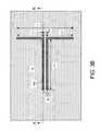
- FIGS. 9A , 9 B, and 9 Dare horizontal cross-sectional views of the first exemplary semiconductor structure along the planes B-B′ and D-D′ of FIG. 9A , respectively.
- FIG. 9Cis a bottom-up view of the first exemplary semiconductor structure of FIGS. 9A , 9 B, and 9 D.
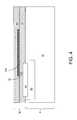
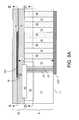
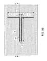
- FIG. 1corresponds to a step after formation of a millimeter wave transceiver 62 on a semiconductor substrate 8 .
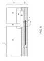
- FIGS. 2A and 2Bcorrespond to a step after deposition of at least one dielectric layer 70 and formation of a pair of metal interconnect structures 78 .
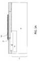
- FIGS. 3A and 3Bcorrespond to a step after formation of an antenna 100 .
- FIG. 4corresponds to a step after formation of a second dielectric layer 80 .
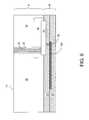
- FIG. 5corresponds to a step after flipping of the first exemplary semiconductor structure upside down and forming at least one through substrate trench 19 .
- FIG. 6corresponds to a step after formation of at least one through substrate conductive via 22 .
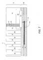
- FIG. 7corresponds to a step after formation of an array of through substrate trenches 29 .
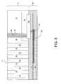
- FIG. 8corresponds to a step after formation of an array of through substrate dielectric vias 30 .
- FIGS. 9A-9Dcorrespond to a step after formation of a reflector plate 200 and
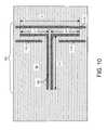
- FIG. 10is a horizontal cross-sectional view of a second exemplary semiconductor structure along a plane equivalent to plane B-B′ of FIG. 9A at a step corresponding to FIGS. 9 A- 9 D according to a second embodiment of the present invention, and shows a first alternative configuration for an antenna.
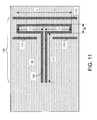
- FIG. 11is a horizontal cross-sectional view of a third exemplary semiconductor structure along a plane equivalent to plane B-B′ of FIG. 9A at a step corresponding to FIGS. 9A-9D according to a third embodiment of the present invention, and shows a second alternative configuration for an antenna.
- FIG. 12is a horizontal cross-sectional view of a fourth exemplary semiconductor structure along a plane equivalent to plane D-D′ of FIG. 9A at a step corresponding to FIGS. 9A-9D according to a fourth embodiment of the present invention, in which an array of through substrate dielectric vias is not present.
- FIG. 13is a flow diagram of a design process used in semiconductor design and manufacture of the semiconductor structures according to the present invention.
- the present inventionrelates to a semiconductor structure including an integrated millimeter wave antenna, a reflector plate, and a transceiver on a substrate, and design structures for the same.
- the articles “a”, “an”, “the” and “said”are intended to mean that there are one or more of the elements.
- the same reference numerals or lettersare used to designate like or equivalent elements. Detailed descriptions of known functions and constructions unnecessarily obscuring the subject matter of the present invention have been omitted for clarity. The drawings are not necessarily drawn to scale.
- a first exemplary semiconductor structurecomprises a semiconductor substrate 8 , which includes a high resistivity semiconductor portion 10 and a low resistivity semiconductor portion 60 .
- the high resistivity semiconductor portion 10 and the low resistivity semiconductor portion 60comprise a single crystalline semiconductor material such as silicon, a silicon germanium alloy region, silicon, germanium, a silicon-germanium alloy region, a silicon carbon alloy region, a silicon-germanium-carbon alloy region, gallium arsenide, indium arsenide, indium gallium arsenide, indium phosphide, lead sulfide, other III-V compound semiconductor materials, and II-VI compound semiconductor materials.
- the single crystalline semiconductor materialmay be silicon.
- the entirety of the high resistivity semiconductor portion 10 and the low resistivity semiconductor portion 60is single crystalline, i.e., has epitaxial atomic alignment.
- the high resistivity semiconductor portion 10has a resistivity greater than 20 Ohms-cm. Preferably, the high resistivity semiconductor portion 10 has a resistivity greater than 1 k Ohms-cm. As will be shown below, a region of the high resistivity semiconductor portion 10 is located between an antenna and a reflector plate, and the eddy current and the accompanying loss is inversely proportional to the resistivity of the semiconductor material in the high resistivity semiconductor portion 10 . While silicon is used herein to illustrate the required dopant level for each threshold resistivity value for the high resistivity semiconductor portion 10 , target dopant concentrations for other semiconductor materials may be readily obtained since each type of semiconductor material has a well established relationship between the dopant concentration and the resistivity of the semiconductor material.
- While the present inventionis described employing a bulk semiconductor substrate, in which the entirety of the high resistivity semiconductor portion 10 and a low resistivity semiconductor portion 60 , use of alternative substrates such as a semiconductor-on-insulator (SOI) substrate, a hybrid substrate including an SOI portion and a bulk portion, and a substrate including a top semiconductor layer and a bottom insulator layer comprising a dielectric material such as silicon oxide or sapphire are also explicitly contemplated herein, which accompanying variations on the structures.
- SOIsemiconductor-on-insulator
- the low resistivity semiconductor portion 60has a resistivity less than 5 Ohm-cm.
- the low resistivity semiconductor portion 60may have a doping of the same conductivity type as the high resistivity semiconductor portion 10 , or may have a doping of the opposite conductivity type as the high resistivity semiconductor portion 10 .
- a reverse biased p-n junctionmay be formed at the interface between the low resistivity semiconductor portion 60 and the high resistivity semiconductor portion 10 to provide electrical isolation.
- the low resistivity semiconductor portion 60has the same conductivity type doping as the high resistivity semiconductor portion 10 , additional well or isolation trenches may be formed within the low resistivity semiconductor portion 60 to provide electrical isolation of devices to be subsequently formed on the low resistivity semiconductor portion 60 .
- the low resistivity semiconductor portion 60may include a portion having a p-type doping and another portion having an n-type doping. Deep trench isolation and/or shallow trench isolation as well as multiple well structures may be employed within the low resistivity semiconductor portion 60 to provide electrical isolation to the devices to be subsequently formed thereupon.
- the low resistivity semiconductor portion 60provides suitably doped semiconductor material for forming semiconductor devices such as field effect transistors, bipolar transistors, diodes, varactors, capacitors, resistors, etc. Since the dopant concentration of the high resistivity semiconductor portion 10 is lower than the dopant concentration of the low resistivity semiconductor portion 60 , the low resistivity semiconductor portion 60 may be formed from a region of the high resistivity semiconductor portion 10 by masked ion implantation. For example, the entirety of the semiconductor substrate 8 may be a high resistivity semiconductor portion 10 , and masked ion implantation into a region on the front surface, or the top surface, of the semiconductor substrate may be employed to form a low resistivity semiconductor portion 60 .
- a millimeter wave transducer 62is formed on the front surface of the low resistivity semiconductor portion 60 .
- the millimeter wave transducer 62converts electromagnetic wave captured by an antenna into an electrical signal for semiconductor devices and/or concerts an electrical signal from semiconductor devices into an electromagnetic wave signal to be broadcast through an antenna.
- the frequency of the electromagnetic wave and the electrical signalsis in the range from about 30 GHz to about 300 GHz.
- the wavelength of the electromagnetic radiation in vacuum corresponding to the electromagnetic waveis from about 1 mm to about 10 mm, i.e., in the millimeter range.
- the millimeter wave transducer 62 and the semiconductor devicesmay be formed employing front-end-of-line processes known in the art.
- the millimeter wave transducer 62 and the semiconductor devicesmay optionally include some back-end-of-line structures such as a metal interconnect structure.
- the millimeter wave transducer 62 and the semiconductor devices on the front surface of the semiconductor substrate 8may include various metal semiconductor alloy regions such as metal silicides.
- At least one dielectric layer 70is formed directly on the front surfaces of the first exemplary semiconductor structure including the top surface of the millimeter wave transducer 62 and other semiconductor devices (not shown).
- the at least one dielectric layer 70may include a middle-of-line (MOL) dielectric layer, at least one back-end-of-line (BEOL) via level dielectric layer, and/or at least one BEOL line level dielectric layer.
- the at least one dielectric layer 70may include a stack of multiple BEOL via level dielectric layers and multiple BEOL line level dielectric layers.
- the at least one dielectric layer 70may comprise silicon oxide, silicon nitride, silicon oxynitride, an organosilicate glass (OSG), low-k chemical vapor deposition (CVD) oxide, a self-planarizing material such as a spin-on glass (SOG), and/or a spin-on low-k dielectric material such as SiLKTM.
- exemplary silicon oxidesinclude undoped silicate glass (USG), borosilicate glass (BSG), phosphosilicate glass (PSG), fluorosilicate glass (FSG), borophosphosilicate glass (BPSG), or a combination thereof.
- the total thickness of the at least one dielectric layermay be from about 100 nm to about 10,000 nm, and typically from about 200 nm to about 5,000 nm.
- a pair of metal interconnect structures 78 that is electrically, i.e., resistively, connected to the millimeter wave transducer 61is formed in the at least one dielectric layer 70 .
- Each metal interconnect structure 78comprises at least one conductive via, and may optionally include additional conductive via(s) and/or at least one metal line structure.
- the number of conductive via(s) and the optional at least one metal line structure in the at least one dielectric layer 70depends on the number of via levels and wiring levels within the at least one dielectric layer 70 .
- the impedance of each component of each of the pair of metal interconnect structures 78is matched to minimize reflection at interfaces between different components, i.e., at interfaces between a conductive via and a conductive line.
- metal interconnect structuresincluding other conductive vias and other conductive metal lines may be formed within the at least one dielectric layer 70 on the millimeter wave transducer 62 and the other semiconductor devices (not shown).
- the top surface of the at least one dielectric layer 70is planar, which may be effected by planarization such as chemical mechanical planarization (CMP).
- CMPchemical mechanical planarization
- a metallic material layeris formed directly on the exposed top surface of the at least one dielectric layer 70 , and is lithographically patterned to form an antenna 100 .
- a photoresist layer(not shown) may be applied over the top surface of the metallic material layer, and lithographically patterned in the shape of an antenna. The pattern in the photoresist is transferred into the metallic material layer by an etch, which may be an anisotropic etch such as a reactive ion etch or an isotropic etch such as a wet etch employing the remaining portions of the photoresist layer as an etch mask.
- the metallic material layermay comprise an elemental metal, a metal alloy, a conductive metallic compound, or a combination thereof.
- Elemental metalsinclude transition metals, Lanthanides, Actinides, alkali metals, alkaline-earth metals, Group III A metals, Group IV A metals, Group V A metals, and Group VI A metals.
- Metal alloysinclude an alloy of at least two of the elemental metals.
- a conductive metallic compoundis a conductive compound of at least one metal and at least one non-metallic element such as TaN, TiN, WN, etc.
- the metallic material layermay comprise Cu, Al, or W.
- the vertical thickness of the antenna 100which is typically substantially the same as the thickness of the metallic material layer, may be from about 0.2 micron to about 10 microns, and typically from about 1 micron to about 5 microns, although lesser and greater thicknesses are also contemplated herein.
- the antenna 100has a width from about 0.2 micron to about 10 microns, and typically from about 1 micron to about 5 microns, although lesser and greater thicknesses are also contemplated herein.
- the entirety of the antenna 100has the same width and the same thickness to insure than the impedance per unit of length remains the same, thereby minimizing internal reflection of waves. In other words, the entirety of the antenna 100 is impedance matched for optimal signal transmission or capture.
- the antenna 100includes a coaxially aligned pair of first antenna portions and a pair of second antenna portions separated by a constant separation distance sd.
- Each of the first antenna portionshas a constant width, which may be from about 10 microns to about 30 microns, and typically from about 1 micron to about 50 microns, although lesser and greater widths are also contemplated herein.
- Each of the first antenna portionshas a first length L 1 , which may be from about 30 microns to about 1,000 microns, although lesser and greater first lengths L 1 are also contemplated herein.
- the separation distance sdmay be from about 0.1 micron to about 30 microns, and, although lesser and greater separation distances are also contemplated herein.
- the length L of the antennais the sum of twice the first length L 1 and the separation distance sd, and is about a quarter wavelength, ⁇ /4, of the electromagnetic signal that the antenna 100 is designed to transmit and/or capture, wherein ⁇ is the full wavelength of the electromagnetic signal.
- the full wavelength ⁇ of the electromagnetic signalrefers to the full wavelength in a dielectric medium, i.e., within the material of the at least one dielectric layer 70 and other surrounding dielectric materials that affects the effective permittivity of the overall dielectric medium in which the antenna 100 is located.
- the permittivity of a materialis the product of a relative permittivity, which is also referred to as a dielectric constant, and the permittivity of the vacuum ⁇ 0 .
- the wavelength of electromagnetic radiation in a mediumis equal to the wavelength of the electromagnetic radiation in vacuum having the same frequency divided by the square root of the relative permittivity of the medium.
- the quarter wavelength of electromagnetic radiation, and consequently, the target dimension for the length L of the antennais the same as the quarter wavelength in vacuum divided by the square root of the dielectric constant of the medium, i.e., 3.9.
- the quarter wavelength in vacuumis from about 250 microns to about 2,500 microns.
- a dielectric constant rangefrom about 2.5, which is about the dielectric constant of a porous low-k chemical vapor deposition (CVD) oxide, to about 8.0, which is the dielectric constant of silicon nitride
- the range of the quarter wavelength in a typical back-end-of-line (BEOL) dielectric layersmay be from about 80 microns to about 1,600 microns.
- the target dimension for the length L of the antennais also from about 80 microns to about 1,600 microns.
- the pair of second antenna portionsruns parallel to each other.
- Each of the second antenna portionshas a second length L 2 , which may be from about 1 micron to about 1,000 microns, and typically from about 200 microns to about 500 microns, although lesser and greater second lengths L 2 are also contemplated herein.
- One end of each of the second antenna portionslaterally abuts, and is directly adjoined to, a proximal end of a first antenna portion.
- the proximal endis the end of an first antenna portion that is closer to the other first antenna portion than the opposite end, which is herein referred to a distal end.
- the length L of the antennais the distance between the two distal ends of the two first antenna portions, and the separation distance sd is the distance of between the two proximal ends of the two first antenna portions.
- Each of the second antenna portionsis connected to the one of the pair of metal interconnect structures 78 near an end located on an opposite side of the end that abuts a first antenna portion.
- the pair of metal interconnect structures 78vertically abuts the antenna 100 .
- the location of the pair of metal interconnect structures 78which underlies the second antenna portion of the antenna 100 , is marked in dotted circles in FIG. 3B .
- the impedance of the pair of metal interconnect structures 78is matched to the impedance of the antenna to minimize reflection of electromagnetic signal transmission from and the antenna 100 to the millimeter wave transceiver 62 .
- another dielectric material layer 80may be formed on the antenna 100 and the exposed surfaces of the at least one dielectric material layer 70 .
- the other dielectric material layer 80may comprise the same type of material as the materials described above for the at least one dielectric material layer 70 .
- the other dielectric material layer 80is optional, and embodiments in which the other dielectric material layer 80 is omitted are also contemplated herein.
- the antenna 100is encapsulated by the at least one dielectric material layer 70 , the pair of metal interconnect structures 78 embedded therein, and the other dielectric material layer 80 .
- the thickness of the other dielectric material layer 80may be from about 1 micron to about 20 microns, and typically from about 2 microns to about 10 microns, although lesser and greater thicknesses are also contemplated herein.
- the other dielectric material layer 80provides the benefit of reducing the wavelength of the electromagnetic signal to be captured by the antenna by a factor on the order of the relative permittivity, i.e., the dielectric constant, of the material of the other dielectric material layer 80 .
- the at least one dielectric material layer 70 and the other dielectric layer 80are collectively called a back-end-of-line (BEOL) dielectric stack 90 .
- BEOLback-end-of-line
- Other metal interconnect structuresmay be formed in the BEOL dielectric stack 90 .
- C4 pads(not shown) or wirebond pads (not shown) may be formed on the front surface, i.e., the top surface, of the BEOL dielectric stack 90 to enable electrical connection of the first exemplary semiconductor structure, which is a semiconductor chip, to other structures such as a chip package.
- the first exemplary semiconductor structureis flipped upside down to place a back surface 11 of the semiconductor substrate 8 on the top.
- At least one through substrate via 19is formed in a region of the high resistivity semiconductor portion 10 that overlie the millimeter wave transducer 62 .
- the at least one through substrate via 19is formed through the high resistivity semiconductor portion 10 and the low resistivity semiconductor portion 60 and exposes a conductive connection component (not shown) in the millimeter wave transducer 62 .
- the conductive connection componentmay be connected to electrical ground of the circuit of the millimeter wave transducer 62 .
- Formation of the at least one through substrate trench 19may be effected by patterning a masking layer (not shown) on the bottom surface of the substrate 8 (which is now located above the body of the semiconductor substrate 8 ) and lithographically patterning the masking layer.
- the pattern in the masking layeris transferred through the semiconductor substrate 8 by an anisotropic etch.
- the masking layermay be a hard mask layer that may be patterned with a photoresist and a pattern transfer by an etch, or a photoresist layer that may be directly patterned with lithographic methods.
- the semiconductor substrate 8may be thinned, for example, by chemical mechanical polishing (CMP), grinding, a chemical etch, cleaving, or other methods.
- CMPchemical mechanical polishing
- the thickness of the semiconductor substrate prior to thinningmay be from about 400 microns to about 750 microns. If the semiconductor substrate 8 is thinned, the thickness of the semiconductor substrate 8 may be reduced to a thickness about 50 microns to about 150 microns.
- the lateral dimensions of the at least one through substrate trench 19may be from about 2 microns to about 100 microns, although lesser and greater dimensions are also contemplated herein.
- a horizontal cross-sectional area of the at least one through substrate trench 19may include a rectangular shape or an elongated ellipsoidal shape.
- sidewalls of the at least one through substrate trench 19by a dimension on the order of 2 microns to about 10 microns to facilitate filling of the at least one through substrate trench 19 with a conductive material in a subsequent step.
- a dielectric liner 20may be formed on the sidewalls of the at least one through substrate trench 19 , for example, by a conformal deposition of a dielectric material, followed by an anisotropic etch that removed horizontal portions of the dielectric material.
- the dielectric liner 20is optional, i.e., may, or may not, be formed. In case the high resistivity semiconductor portion 10 has sufficiently high resistivity to effectively function as an insulating material, the dielectric liner 20 may be omitted.
- At least one through substrate conductive via 22is formed in the remaining cavity of the at least one through substrate trench 19 by deposition of a conducive material by chemical vapor deposition (CVD), physical vapor deposition (PVD), electroplating, electroless plating, or a combination thereof. Excess conductive material on the back surface 11 of the substrate 8 is removed by a recess etch, chemical mechanical planarization (CMP), or a combination thereof.
- the at least one through substrate conductive via 22provide an electrically conductive path between the back surface 11 of the semiconductor substrate 8 and the millimeter wave transceiver 62 .
- an array of through substrate trenches 29is formed in the semiconductor substrate 8 .
- the array of through substrate trenches 29is formed in a region of the high resistivity semiconductor portion 10 that does not overlie the low resistivity semiconductor portion 60 .
- the entirety of the sidewalls of the array of the through substrate trenches 29have high resistivity semiconductor materials from the high resistivity semiconductor portion 10 .
- each through substrate trench in the array of through substrate trenches 29may be from about 2 microns to about 100 microns, although lesser and greater dimensions are also contemplated herein.
- Each through substrate trenchesmay have a horizontal cross-sectional shape that is a rectangle or an elongated ellipsoid.
- sidewalls of each through substrate trench 29are separated by a dimension on the order of 2 microns to about 10 microns to facilitate filling of the array of through substrate trenches 29 with a dielectric material in a subsequent step.
- the array of through substrate trenches 29is filled by a conformal deposition of a dielectric material, for example, by chemical vapor deposition (CVD) or a spin-on coating.
- CVDchemical vapor deposition
- CMPchemical mechanical planarization
- the dielectric materialhas a dielectric constant less than the dielectric constant of the semiconductor material in the high resistivity semiconductor portion 10 .
- the dielectric constant of the high resistivity semiconductor portion 10is about 11.9 at a frequency range from about 30 GHz to about 300 GHz.
- the dielectric materialmay comprise silicon nitride having a dielectric constant of about 7.5.
- the dielectric materialhas a dielectric constant less than 4.0.
- the dielectric materialmay be silicon oxide, which has a dielectric constant of about 3.9.
- the dielectric materialmay be an organosilicate glass (OSG), low-k chemical vapor deposition (CVD) oxide, or a spin-on low-k dielectric material such as SiLKTM, which has a dielectric constant less than 3.0.
- the dielectric materialmay be a porous low-k dielectric material.
- the effect of the array of through substrate dielectric vias 30is to lower the effective dielectric constant of the region including the array of through substrate dielectric vias 30 and the sub-portion, or a matrix, of the high resistivity semiconductor portion 10 that embeds the array of through substrate dielectric vias 30 .
- the lower the dielectric constant of the array of through substrate dielectric vias 30the lower the effective dielectric constant of the region including the array of through substrate dielectric vias 30 .
- the sum of the thickness of the substrate 8 and the thickness of the at least one dielectric layer 70is about a quarter wavelength of the electromagnetic signal to be captured and/or transmitted by the antenna.
- a low effective dielectric constant for the region including the array of through substrate dielectric vias 30allows less thinning of the semiconductor substrate 8 , or even elimination of thinning of the semiconductor substrate 8 .
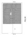
- FIGS. 9A-9Da reflector plate 200 is formed directly on the back surface 11 of the semiconductor substrate.
- FIG. 9Ais a vertical cross-sectional view.
- FIGS. 9B and 9Dare horizontal cross-sectional views of the first exemplary semiconductor structure along the planes B-B′ and D-D′ of FIG. 9A , respectively.
- FIG. 9Cis a bottom-up view of the first exemplary semiconductor structure of FIGS. 9A , 9 B, and 9 D.
- the reflector plate 200may be formed by formation of a metallic conductive layer, for example, by chemical vapor deposition (CVD), physical vapor deposition (PVD), electroplating, electroless plating, or a combination thereof.
- the metallic conductive layermay be lithographically patterned to form the reflector plate 200 .
- the reflector plate 200comprises a metallic material such as copper, aluminum, tungsten, gold, silver, bronze, etc.
- the thickness of the reflector plate 200is greater than the skin depth of the metallic material comprising the reflector plate 200 . More preferably, the thickness of the reflector plate 200 is at least a multiple of the skin depth of the metallic material comprising the reflector plate 200 .
- the skin depthis inversely proportional to the square root of the frequency of the electromagnetic signal. For an electromagnetic signal at 100 GHz, the skin depths of aluminum, copper, gold, and silver are 0.26 micron, 0.21 micron, 0.26 micron, and 0.20 micron.
- the thickness of the reflector plate 200is from about 2 micron to about 20 microns, and typically about 10 microns, although lesser and greater thicknesses are also contemplated herein.
- the reflector plate 200is formed directly on the at least one through substrate conductive via 22 , thereby being electrically connected to the millimeter wave transceiver 62 , and typically to electrical ground of the circuit in the millimeter wave transceiver 62 .
- the reflector plate 200is formed directly on the array of the through substrate dielectric vias 30 .
- the entirety of the coaxially aligned pair of first antenna portions of the antenna 100overlies the reflector plate 200 .
- the reflector plate 200reflects the electromagnetic signal that the antenna 100 transmits or captures, thereby enhancing the effectiveness of the antenna 100 .
- Proper placement of the reflector plate 200may increase the effectiveness of the antenna up to a factor of 4, and enhance the directionality of transmission of electromagnetic signal.
- the spacing s between the antenna 100 and the reflector plate 200needs to be about a quarter wavelength of the electromagnetic signal in the medium between the antenna 100 and the reflector plate 200 .
- the quarter wavelength in vacuumis from about 250 microns to about 2,500 microns.
- a dielectric constantrange from about 2.5, which is about the dielectric constant of a porous low-k chemical vapor deposition (CVD) oxide, to about 8.0, which would be obtained if the array of the through substrate dielectric vias 30 is filled with silicon oxide having a dielectric constant of 3.9 and the high resistivity semiconductor portion comprise silicon having a dielectric constant of 11.9 at 100 GHz, and the volume of the silicon oxide is about 50% of the total volume between the antenna 100 and the reflector plate 200 , the equivalent dielectric constant between 100 and 200 can be around 7 to 8, the range of the quarter wavelength in the equivalent dielectric constant may be from about 90 microns to about 900 microns.
- CVDchemical vapor deposition
- a practical range for the spacing s between the antenna 100 and the reflector plate 200is from about 50 microns to about 750 microns, which is within the range of thickness for semiconductor substrate 8 that may be obtained without thinning or with thinning.
- FIG. 10a horizontal cross-sectional view of a second exemplary semiconductor structure along a plane equivalent to plane B-B′ of FIG. 9A is shown at a step corresponding to FIGS. 9A-9D according to a second embodiment of the present invention.
- the second exemplary semiconductor structureis derived from the first exemplary semiconductor structure by modifying the pattern of remaining portions of the metallic material layer from which the antenna 100 is patterned at the step of the first embodiment corresponding to FIGS. 3A and 3B .
- a first alternative antenna 101which is a first alternative configuration for an antenna, is formed in the second embodiment instead of the antenna 100 in the first embodiment.
- the first alternative antenna 100comprises the antenna 100 as in the first embodiment and antenna waveguide portions 110 , which improves directionality for transmission and reception of electromagnetic signals. Additional antenna waveguide portions may be optionally formed.
- FIG. 11a horizontal cross-sectional view of a third exemplary semiconductor structure along a plane equivalent to plane B-B′ of FIG. 9A is shown at a step corresponding to FIGS. 9A-9D according to a third embodiment of the present invention.
- the third exemplary semiconductor structureis derived from the first exemplary semiconductor structure by modifying the pattern of remaining portions of the metallic material layer from which the antenna 100 is patterned at the step of the first embodiment corresponding to FIGS. 3A and 3B .
- a second alternative antenna 102which is a second alternative configuration for an antenna, is formed in the third embodiment instead of the antenna 100 in the first embodiment.
- the second alternative antenna 102comprises a closed loop antenna 100 ′ and antenna waveguide portions 110 , which improves directionality for transmission and reception of electromagnetic signals.
- the closed loop antenna 100 ′include all portions of the antenna 100 in the first embodiment as well as a pair of transverse extension portions directly abutting the distal ends of the antenna 100 of the first embodiment and a longitudinal portion directly abutting ends of the pair of transverse extension portions. Additional antenna waveguide portions may be optionally formed.
- FIG. 12a horizontal cross-sectional view of a fourth exemplary semiconductor structure along a plane equivalent to plane D-D′ of FIG. 9A is shown at a step corresponding to FIGS. 9A-9D according to a fourth embodiment of the present invention.
- formation of the array of the through substrate trenches 29 and the array of the through substrate dielectric vias 30is omitted from the first embodiment.
- the dielectric constant of the high resistivity semiconductor portion 10 between the reflector plate 200 and the antenna 100remain unchanged.
- the semiconductor substrate 8is thinned to a thickness from about 50 ⁇ m to about 200 ⁇ m, or to a thickness less than 50 ⁇ m that is technically feasible.
- This configurationmay be employed for a limited frequency range, for example, from about 30 GHz to about 120 GHz of the millimeter wave range.
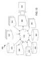
- FIG. 13shows a block diagram of an exemplary design flow 900 used for example, in semiconductor IC logic design, simulation, test, layout, and manufacture.
- Design flow 900includes processes and mechanisms for processing design structures or devices to generate logically or otherwise functionally equivalent representations of the design structures and/or devices described above and shown in FIGS. 1 , 2 A, 2 B, 3 A, 3 B, 4 - 8 , 9 A- 9 D, and 10 - 12 .
- the design structures processes and/or generated by design flow 900may be encoded on machine-readable transmission or storage media to include data and/or instructions that, when executed or otherwise processes on a data processing system, generate a logically, structurally, mechanically, or otherwise functionally equivalent representation of hardware components, circuits, devices, or systems.
- Design flow 900may vary depending on the type of representation being designed. For example, a design flow for building an application specific integrated circuit (ASIC) may differ from a design flow 900 for designing a standard component or from a design flow 900 for instantiating the design into a programmable array, for example, a programmable gate array (PGA) or a field programmable gate array (FPGA) offered by Altera® Inc. or Xilinx® Inc.
- ASICapplication specific integrated circuit
- PGAprogrammable gate array
- FPGAfield programmable gate array
- FIG. 13illustrates multiple such design structures including an input design structure 920 that is preferably processed by design process 910 .
- Design structure 920may be a logical simulation design structure generated and processed by design process 910 to produce a logically equivalent functional representation of a hardware device.
- Design structure 920may also, or alternately, comprise data and/or program instructions that, when processed by design process 910 , generate a functional representation of the physical structure of a hardware device.
- design structure 920may be generated using electronic computer-aided design (ECAD) such as implemented by a core developer/designer.
- ECADelectronic computer-aided design
- design structure 920When encoded on a machine-readable data transmission, gate array, or storage medium, design structure 920 may be accessed and processed by one or more hardware and/or software modules within design process 910 to simulate or otherwise functionally represent an electronic component, circuit, electronic or logic module, apparatus, device, or system such as those shown in FIGS. 1 , 2 A, 2 B, 3 A, 3 B, 4 - 8 , 9 A- 9 D, and 10 - 12 .
- design structure 920may comprise files or other data structures including human and/or machine-readable source code, compiled structures, and computer-executable code structures that when processed by a design or simulation data processing system, functionally simulate or otherwise represent circuits or other levels of hardware logic design.
- Such data structuresmay include hardware-description language (HDL) design entities or other data structures conforming to and/or compatible with lower-level HDL design languages such as Verilog and VHDL, and/or higher level design languages such as C or C++.
- HDLhardware-description language
- Design process 910preferably employs and incorporates hardware and/or software modules for synthesizing, translating, or otherwise processing a design/simulation functional equivalent of the components, circuits, devices, or logic structures shown in FIGS. 1 , 2 A, 2 B, 3 A, 3 B, 4 - 8 , 9 A- 9 D, and 10 - 12 to generate a netlist 980 which may contain design structures such as design structure 920 .
- Netlist 980may comprise, for example, compiled or otherwise processed data structures representing a list of wires, discrete components, logic gates, control circuits, I/O devices, models, etc. that describes the connections to other elements and circuits in an integrated circuit design.
- Netlist 980may be synthesized using an iterative process in which netlist 980 is resynthesized one or more times depending on design specifications and parameters for the device. As with other design structure types described herein, netlist 980 may be recorded on a machine-readable data storage medium or programmed into a programmable gate array.
- the mediummay be a non-volatile storage medium such as a magnetic or optical disk drive, a programmable gate array, a compact flash, or other flash memory. Additionally, or in the alternative, the medium may be a system or cache memory, buffer space, or electrically or optically conductive devices and materials on which data packets may be transmitted and intermediately stored via the Internet, or other networking suitable means.
- Design process 910may include hardware and software modules for processing a variety of input data structure types including netlist 980 .
- data structure typesmay reside, for example, within library elements 930 and include a set of commonly used elements, circuits, and devices, including models, layouts, and symbolic representations, for a given manufacturing technology (e.g., different technology nodes, 32 nm, 45 nm, 90 nm, etc.).
- the data structure typesmay further include design specifications 940 , characterization data 950 , verification data 960 , design rules 970 , and test data files 985 which may include input test patterns, output test results, and other testing information.
- Design process 910may further include, for example, standard mechanical design processes such as stress analysis, thermal analysis, mechanical event simulation, process simulation for operations such as casting, molding, and die press forming, etc.
- standard mechanical design processessuch as stress analysis, thermal analysis, mechanical event simulation, process simulation for operations such as casting, molding, and die press forming, etc.
- One of ordinary skill in the art of mechanical designcan appreciate the extent of possible mechanical design tools and applications used in design process 910 without deviating from the scope and spirit of the invention.
- Design process 910may also include modules for performing standard circuit design processes such as timing analysis, verification, design rule checking, place and route operations, etc.
- Design process 910employs and incorporates logic and physical design tools such as HDL compilers and simulation model build tools to process design structure 920 together with some or all of the depicted supporting data structures along with any additional mechanical design or data (if applicable), to generate a second design structure 990 .
- Design structure 990resides on a storage medium or programmable gate array in a data format used for the exchange of data of mechanical devices and structures (e.g. information stored in an IGES, DXF, Parasolid XT, JT, DRG, or any other suitable format for storing or rendering such mechanical design structures).
- design structure 990preferably comprises one or more files, data structures, or other computer-encoded data or instructions that reside on transmission or data storage media and that when processed by an ECAD system generate a logically or otherwise functionally equivalent form of one or more of the embodiments of the invention shown in FIGS. 1 , 2 A, 2 B, 3 A, 3 B, 4 - 8 , 9 A- 9 D, and 10 - 12 .
- design structure 990may comprise a compiled, executable HDL simulation model that functionally simulates the devices shown in FIGS. 1 , 2 A, 2 B, 3 A, 3 B, 4 - 8 , 9 A- 9 D, and 10 - 12 .
- Design structure 990may also employ a data format used for the exchange of layout data of integrated circuits and/or symbolic data format (e.g. information stored in a GDSII (GDS2), GL1, OASIS, map files, or any other suitable format for storing such design data structures).
- Design structure 990may comprise information such as, for example, symbolic data, map files, test data files, design content files, manufacturing data, layout parameters, wires, levels of metal, vias, shapes, data for routing through the manufacturing line, and any other data required by a manufacturer or other designer/developer to produce a device or structure as described above and shown in FIGS. 1 , 2 A, 2 B, 3 A, 3 B, 4 - 8 , 9 A- 9 D, and 10 - 12 .
- Design structure 990may then proceed to a stage 995 where, for example, design structure 990 : proceeds to tape-out, is released to manufacturing, is released to a mask house, is sent to another design house, is sent back to the customer, etc.
Landscapes
- Engineering & Computer Science (AREA)
- Microelectronics & Electronic Packaging (AREA)
- Aerials With Secondary Devices (AREA)
- Semiconductor Integrated Circuits (AREA)
Abstract
Description
Claims (17)
Priority Applications (2)
| Application Number | Priority Date | Filing Date | Title |
|---|---|---|---|
| US12/187,442US8232920B2 (en) | 2008-08-07 | 2008-08-07 | Integrated millimeter wave antenna and transceiver on a substrate |
| US13/534,350US8519892B2 (en) | 2008-08-07 | 2012-06-27 | Integrated millimeter wave antenna and transceiver on a substrate |
Applications Claiming Priority (1)
| Application Number | Priority Date | Filing Date | Title |
|---|---|---|---|
| US12/187,442US8232920B2 (en) | 2008-08-07 | 2008-08-07 | Integrated millimeter wave antenna and transceiver on a substrate |
Related Child Applications (1)
| Application Number | Title | Priority Date | Filing Date |
|---|---|---|---|
| US13/534,350DivisionUS8519892B2 (en) | 2008-08-07 | 2012-06-27 | Integrated millimeter wave antenna and transceiver on a substrate |
Publications (2)
| Publication Number | Publication Date |
|---|---|
| US20100033395A1 US20100033395A1 (en) | 2010-02-11 |
| US8232920B2true US8232920B2 (en) | 2012-07-31 |
Family
ID=41652431
Family Applications (2)
| Application Number | Title | Priority Date | Filing Date |
|---|---|---|---|
| US12/187,442Active2031-04-30US8232920B2 (en) | 2008-08-07 | 2008-08-07 | Integrated millimeter wave antenna and transceiver on a substrate |
| US13/534,350ActiveUS8519892B2 (en) | 2008-08-07 | 2012-06-27 | Integrated millimeter wave antenna and transceiver on a substrate |
Family Applications After (1)
| Application Number | Title | Priority Date | Filing Date |
|---|---|---|---|
| US13/534,350ActiveUS8519892B2 (en) | 2008-08-07 | 2012-06-27 | Integrated millimeter wave antenna and transceiver on a substrate |
Country Status (1)
| Country | Link |
|---|---|
| US (2) | US8232920B2 (en) |
Cited By (8)
| Publication number | Priority date | Publication date | Assignee | Title |
|---|---|---|---|---|
| US20100201579A1 (en)* | 2009-01-02 | 2010-08-12 | Das Nirod K | Using dielectric substrates, embedded with vertical wire structures, with slotline and microstrip elements to eliminate parallel-plate or surface-wave radiation in printed-circuits, chip packages and antennas |
| US20120086114A1 (en)* | 2010-10-07 | 2012-04-12 | Broadcom Corporation | Millimeter devices on an integrated circuit |
| US20120266116A1 (en)* | 2008-08-07 | 2012-10-18 | International Business Machines Corporation | Integrated millimeter wave antenna and transceiver on a substrate |
| US20140198008A1 (en)* | 2009-09-16 | 2014-07-17 | Michael Clyde Walker | Passive repeater for wireless communications |
| US20150042420A1 (en)* | 2013-08-06 | 2015-02-12 | The United States Government As Represented By The | Optically transparent, radio frequency, planar transmission lines |
| CN105934851A (en)* | 2014-01-08 | 2016-09-07 | 高通股份有限公司 | Quasi-yagi-type antenna |
| US9472859B2 (en) | 2014-05-20 | 2016-10-18 | International Business Machines Corporation | Integration of area efficient antennas for phased array or wafer scale array antenna applications |
| CN108933121A (en)* | 2017-05-24 | 2018-12-04 | 日月光半导体制造股份有限公司 | Semiconductor packaging device |
Families Citing this family (177)
| Publication number | Priority date | Publication date | Assignee | Title |
|---|---|---|---|---|
| US7724194B2 (en)* | 2006-06-30 | 2010-05-25 | Motorola, Inc. | Dual autodiplexing antenna |
| WO2013147744A1 (en)* | 2012-03-26 | 2013-10-03 | Intel Corporation | Integration of millimeter wave antennas on microelectronic substrates |
| US9577314B2 (en)* | 2012-09-12 | 2017-02-21 | International Business Machines Corporation | Hybrid on-chip and package antenna |
| EP2901523B1 (en)* | 2012-09-26 | 2016-09-07 | Omniradar B.V. | Radiofrequency module |
| US10009065B2 (en) | 2012-12-05 | 2018-06-26 | At&T Intellectual Property I, L.P. | Backhaul link for distributed antenna system |
| US9113347B2 (en) | 2012-12-05 | 2015-08-18 | At&T Intellectual Property I, Lp | Backhaul link for distributed antenna system |
| DE102013202806B4 (en)* | 2013-01-31 | 2025-07-24 | Rohde & Schwarz GmbH & Co. Kommanditgesellschaft | Circuit on thin substrate for use in waveguides and manufacturing processes |
| US9525524B2 (en) | 2013-05-31 | 2016-12-20 | At&T Intellectual Property I, L.P. | Remote distributed antenna system |
| US9999038B2 (en) | 2013-05-31 | 2018-06-12 | At&T Intellectual Property I, L.P. | Remote distributed antenna system |
| US20150207216A1 (en)* | 2013-06-04 | 2015-07-23 | Panasonic Intellectual Property Management Co., Ltd. | Wireless module |
| US9570809B2 (en) | 2013-06-06 | 2017-02-14 | Qualcomm Incorporated | Techniques for designing millimeter wave printed dipole antennas |
| EP3058663B1 (en)* | 2013-10-18 | 2022-09-14 | Molex, LLC | Contactless communication unit connector assemblies with signal directing structures |
| US8897697B1 (en) | 2013-11-06 | 2014-11-25 | At&T Intellectual Property I, Lp | Millimeter-wave surface-wave communications |
| US9209902B2 (en) | 2013-12-10 | 2015-12-08 | At&T Intellectual Property I, L.P. | Quasi-optical coupler |
| US9692101B2 (en) | 2014-08-26 | 2017-06-27 | At&T Intellectual Property I, L.P. | Guided wave couplers for coupling electromagnetic waves between a waveguide surface and a surface of a wire |
| US9768833B2 (en) | 2014-09-15 | 2017-09-19 | At&T Intellectual Property I, L.P. | Method and apparatus for sensing a condition in a transmission medium of electromagnetic waves |
| US10063280B2 (en) | 2014-09-17 | 2018-08-28 | At&T Intellectual Property I, L.P. | Monitoring and mitigating conditions in a communication network |
| US9615269B2 (en) | 2014-10-02 | 2017-04-04 | At&T Intellectual Property I, L.P. | Method and apparatus that provides fault tolerance in a communication network |
| US9685992B2 (en) | 2014-10-03 | 2017-06-20 | At&T Intellectual Property I, L.P. | Circuit panel network and methods thereof |
| US9503189B2 (en) | 2014-10-10 | 2016-11-22 | At&T Intellectual Property I, L.P. | Method and apparatus for arranging communication sessions in a communication system |
| US9762289B2 (en) | 2014-10-14 | 2017-09-12 | At&T Intellectual Property I, L.P. | Method and apparatus for transmitting or receiving signals in a transportation system |
| US9973299B2 (en) | 2014-10-14 | 2018-05-15 | At&T Intellectual Property I, L.P. | Method and apparatus for adjusting a mode of communication in a communication network |
| US9780834B2 (en) | 2014-10-21 | 2017-10-03 | At&T Intellectual Property I, L.P. | Method and apparatus for transmitting electromagnetic waves |
| US9520945B2 (en) | 2014-10-21 | 2016-12-13 | At&T Intellectual Property I, L.P. | Apparatus for providing communication services and methods thereof |
| US9312919B1 (en) | 2014-10-21 | 2016-04-12 | At&T Intellectual Property I, Lp | Transmission device with impairment compensation and methods for use therewith |
| US9653770B2 (en) | 2014-10-21 | 2017-05-16 | At&T Intellectual Property I, L.P. | Guided wave coupler, coupling module and methods for use therewith |
| US9627768B2 (en) | 2014-10-21 | 2017-04-18 | At&T Intellectual Property I, L.P. | Guided-wave transmission device with non-fundamental mode propagation and methods for use therewith |
| US9577306B2 (en) | 2014-10-21 | 2017-02-21 | At&T Intellectual Property I, L.P. | Guided-wave transmission device and methods for use therewith |
| US9769020B2 (en) | 2014-10-21 | 2017-09-19 | At&T Intellectual Property I, L.P. | Method and apparatus for responding to events affecting communications in a communication network |
| US10770802B2 (en)* | 2014-11-10 | 2020-09-08 | Qorvo Us, Inc. | Antenna on a device assembly |
| US9544006B2 (en) | 2014-11-20 | 2017-01-10 | At&T Intellectual Property I, L.P. | Transmission device with mode division multiplexing and methods for use therewith |
| US9997819B2 (en) | 2015-06-09 | 2018-06-12 | At&T Intellectual Property I, L.P. | Transmission medium and method for facilitating propagation of electromagnetic waves via a core |
| US9800327B2 (en) | 2014-11-20 | 2017-10-24 | At&T Intellectual Property I, L.P. | Apparatus for controlling operations of a communication device and methods thereof |
| US10009067B2 (en) | 2014-12-04 | 2018-06-26 | At&T Intellectual Property I, L.P. | Method and apparatus for configuring a communication interface |
| US9954287B2 (en) | 2014-11-20 | 2018-04-24 | At&T Intellectual Property I, L.P. | Apparatus for converting wireless signals and electromagnetic waves and methods thereof |
| US10243784B2 (en) | 2014-11-20 | 2019-03-26 | At&T Intellectual Property I, L.P. | System for generating topology information and methods thereof |
| US9654173B2 (en) | 2014-11-20 | 2017-05-16 | At&T Intellectual Property I, L.P. | Apparatus for powering a communication device and methods thereof |
| US9461706B1 (en) | 2015-07-31 | 2016-10-04 | At&T Intellectual Property I, Lp | Method and apparatus for exchanging communication signals |
| US9680670B2 (en) | 2014-11-20 | 2017-06-13 | At&T Intellectual Property I, L.P. | Transmission device with channel equalization and control and methods for use therewith |
| US9742462B2 (en) | 2014-12-04 | 2017-08-22 | At&T Intellectual Property I, L.P. | Transmission medium and communication interfaces and methods for use therewith |
| US10340573B2 (en) | 2016-10-26 | 2019-07-02 | At&T Intellectual Property I, L.P. | Launcher with cylindrical coupling device and methods for use therewith |
| US9424389B2 (en)* | 2014-12-18 | 2016-08-23 | International Business Machines Corporation | Implementing enhanced performance dynamic evaluation circuit by combining precharge and delayed keeper |
| EP3251167B1 (en) | 2015-01-27 | 2020-07-15 | AT & S Austria Technologie & Systemtechnik Aktiengesellschaft | Component carrier with integrated antenna structure |
| US10144036B2 (en) | 2015-01-30 | 2018-12-04 | At&T Intellectual Property I, L.P. | Method and apparatus for mitigating interference affecting a propagation of electromagnetic waves guided by a transmission medium |
| US9876570B2 (en) | 2015-02-20 | 2018-01-23 | At&T Intellectual Property I, Lp | Guided-wave transmission device with non-fundamental mode propagation and methods for use therewith |
| US9749013B2 (en) | 2015-03-17 | 2017-08-29 | At&T Intellectual Property I, L.P. | Method and apparatus for reducing attenuation of electromagnetic waves guided by a transmission medium |
| US9728838B2 (en)* | 2015-04-15 | 2017-08-08 | Globalfoundries Inc. | On chip antenna with opening |
| US10224981B2 (en) | 2015-04-24 | 2019-03-05 | At&T Intellectual Property I, Lp | Passive electrical coupling device and methods for use therewith |
| US9705561B2 (en) | 2015-04-24 | 2017-07-11 | At&T Intellectual Property I, L.P. | Directional coupling device and methods for use therewith |
| US9793954B2 (en) | 2015-04-28 | 2017-10-17 | At&T Intellectual Property I, L.P. | Magnetic coupling device and methods for use therewith |
| US9948354B2 (en) | 2015-04-28 | 2018-04-17 | At&T Intellectual Property I, L.P. | Magnetic coupling device with reflective plate and methods for use therewith |
| US9748626B2 (en) | 2015-05-14 | 2017-08-29 | At&T Intellectual Property I, L.P. | Plurality of cables having different cross-sectional shapes which are bundled together to form a transmission medium |
| US9871282B2 (en) | 2015-05-14 | 2018-01-16 | At&T Intellectual Property I, L.P. | At least one transmission medium having a dielectric surface that is covered at least in part by a second dielectric |
| US9490869B1 (en) | 2015-05-14 | 2016-11-08 | At&T Intellectual Property I, L.P. | Transmission medium having multiple cores and methods for use therewith |
| US10650940B2 (en) | 2015-05-15 | 2020-05-12 | At&T Intellectual Property I, L.P. | Transmission medium having a conductive material and methods for use therewith |
| US9917341B2 (en) | 2015-05-27 | 2018-03-13 | At&T Intellectual Property I, L.P. | Apparatus and method for launching electromagnetic waves and for modifying radial dimensions of the propagating electromagnetic waves |
| US10812174B2 (en) | 2015-06-03 | 2020-10-20 | At&T Intellectual Property I, L.P. | Client node device and methods for use therewith |
| US9866309B2 (en) | 2015-06-03 | 2018-01-09 | At&T Intellectual Property I, Lp | Host node device and methods for use therewith |
| US9912381B2 (en) | 2015-06-03 | 2018-03-06 | At&T Intellectual Property I, Lp | Network termination and methods for use therewith |
| US10103801B2 (en) | 2015-06-03 | 2018-10-16 | At&T Intellectual Property I, L.P. | Host node device and methods for use therewith |
| US9913139B2 (en) | 2015-06-09 | 2018-03-06 | At&T Intellectual Property I, L.P. | Signal fingerprinting for authentication of communicating devices |
| US10142086B2 (en) | 2015-06-11 | 2018-11-27 | At&T Intellectual Property I, L.P. | Repeater and methods for use therewith |
| US9608692B2 (en) | 2015-06-11 | 2017-03-28 | At&T Intellectual Property I, L.P. | Repeater and methods for use therewith |
| US9820146B2 (en) | 2015-06-12 | 2017-11-14 | At&T Intellectual Property I, L.P. | Method and apparatus for authentication and identity management of communicating devices |
| US9667317B2 (en) | 2015-06-15 | 2017-05-30 | At&T Intellectual Property I, L.P. | Method and apparatus for providing security using network traffic adjustments |
| US9509415B1 (en) | 2015-06-25 | 2016-11-29 | At&T Intellectual Property I, L.P. | Methods and apparatus for inducing a fundamental wave mode on a transmission medium |
| US9865911B2 (en) | 2015-06-25 | 2018-01-09 | At&T Intellectual Property I, L.P. | Waveguide system for slot radiating first electromagnetic waves that are combined into a non-fundamental wave mode second electromagnetic wave on a transmission medium |
| US9640850B2 (en) | 2015-06-25 | 2017-05-02 | At&T Intellectual Property I, L.P. | Methods and apparatus for inducing a non-fundamental wave mode on a transmission medium |
| US9847566B2 (en) | 2015-07-14 | 2017-12-19 | At&T Intellectual Property I, L.P. | Method and apparatus for adjusting a field of a signal to mitigate interference |
| US10033108B2 (en) | 2015-07-14 | 2018-07-24 | At&T Intellectual Property I, L.P. | Apparatus and methods for generating an electromagnetic wave having a wave mode that mitigates interference |
| US9628116B2 (en) | 2015-07-14 | 2017-04-18 | At&T Intellectual Property I, L.P. | Apparatus and methods for transmitting wireless signals |
| US10205655B2 (en) | 2015-07-14 | 2019-02-12 | At&T Intellectual Property I, L.P. | Apparatus and methods for communicating utilizing an antenna array and multiple communication paths |
| US10320586B2 (en) | 2015-07-14 | 2019-06-11 | At&T Intellectual Property I, L.P. | Apparatus and methods for generating non-interfering electromagnetic waves on an insulated transmission medium |
| US9836957B2 (en) | 2015-07-14 | 2017-12-05 | At&T Intellectual Property I, L.P. | Method and apparatus for communicating with premises equipment |
| US9722318B2 (en) | 2015-07-14 | 2017-08-01 | At&T Intellectual Property I, L.P. | Method and apparatus for coupling an antenna to a device |
| US10148016B2 (en) | 2015-07-14 | 2018-12-04 | At&T Intellectual Property I, L.P. | Apparatus and methods for communicating utilizing an antenna array |
| US9853342B2 (en) | 2015-07-14 | 2017-12-26 | At&T Intellectual Property I, L.P. | Dielectric transmission medium connector and methods for use therewith |
| US10044409B2 (en) | 2015-07-14 | 2018-08-07 | At&T Intellectual Property I, L.P. | Transmission medium and methods for use therewith |
| US10170840B2 (en) | 2015-07-14 | 2019-01-01 | At&T Intellectual Property I, L.P. | Apparatus and methods for sending or receiving electromagnetic signals |
| US9882257B2 (en) | 2015-07-14 | 2018-01-30 | At&T Intellectual Property I, L.P. | Method and apparatus for launching a wave mode that mitigates interference |
| US10341142B2 (en) | 2015-07-14 | 2019-07-02 | At&T Intellectual Property I, L.P. | Apparatus and methods for generating non-interfering electromagnetic waves on an uninsulated conductor |
| US10033107B2 (en) | 2015-07-14 | 2018-07-24 | At&T Intellectual Property I, L.P. | Method and apparatus for coupling an antenna to a device |
| US9608740B2 (en) | 2015-07-15 | 2017-03-28 | At&T Intellectual Property I, L.P. | Method and apparatus for launching a wave mode that mitigates interference |
| US10090606B2 (en) | 2015-07-15 | 2018-10-02 | At&T Intellectual Property I, L.P. | Antenna system with dielectric array and methods for use therewith |
| US9793951B2 (en) | 2015-07-15 | 2017-10-17 | At&T Intellectual Property I, L.P. | Method and apparatus for launching a wave mode that mitigates interference |
| US10784670B2 (en) | 2015-07-23 | 2020-09-22 | At&T Intellectual Property I, L.P. | Antenna support for aligning an antenna |
| US9749053B2 (en) | 2015-07-23 | 2017-08-29 | At&T Intellectual Property I, L.P. | Node device, repeater and methods for use therewith |
| US9871283B2 (en) | 2015-07-23 | 2018-01-16 | At&T Intellectual Property I, Lp | Transmission medium having a dielectric core comprised of plural members connected by a ball and socket configuration |
| US9912027B2 (en) | 2015-07-23 | 2018-03-06 | At&T Intellectual Property I, L.P. | Method and apparatus for exchanging communication signals |
| US9948333B2 (en) | 2015-07-23 | 2018-04-17 | At&T Intellectual Property I, L.P. | Method and apparatus for wireless communications to mitigate interference |
| US9735833B2 (en) | 2015-07-31 | 2017-08-15 | At&T Intellectual Property I, L.P. | Method and apparatus for communications management in a neighborhood network |
| US10020587B2 (en) | 2015-07-31 | 2018-07-10 | At&T Intellectual Property I, L.P. | Radial antenna and methods for use therewith |
| US9967173B2 (en) | 2015-07-31 | 2018-05-08 | At&T Intellectual Property I, L.P. | Method and apparatus for authentication and identity management of communicating devices |
| US9904535B2 (en) | 2015-09-14 | 2018-02-27 | At&T Intellectual Property I, L.P. | Method and apparatus for distributing software |
| US10009901B2 (en) | 2015-09-16 | 2018-06-26 | At&T Intellectual Property I, L.P. | Method, apparatus, and computer-readable storage medium for managing utilization of wireless resources between base stations |
| US10009063B2 (en) | 2015-09-16 | 2018-06-26 | At&T Intellectual Property I, L.P. | Method and apparatus for use with a radio distributed antenna system having an out-of-band reference signal |
| US10136434B2 (en) | 2015-09-16 | 2018-11-20 | At&T Intellectual Property I, L.P. | Method and apparatus for use with a radio distributed antenna system having an ultra-wideband control channel |
| US10079661B2 (en) | 2015-09-16 | 2018-09-18 | At&T Intellectual Property I, L.P. | Method and apparatus for use with a radio distributed antenna system having a clock reference |
| US9769128B2 (en) | 2015-09-28 | 2017-09-19 | At&T Intellectual Property I, L.P. | Method and apparatus for encryption of communications over a network |
| US9729197B2 (en) | 2015-10-01 | 2017-08-08 | At&T Intellectual Property I, L.P. | Method and apparatus for communicating network management traffic over a network |
| US9876264B2 (en) | 2015-10-02 | 2018-01-23 | At&T Intellectual Property I, Lp | Communication system, guided wave switch and methods for use therewith |
| US9882277B2 (en) | 2015-10-02 | 2018-01-30 | At&T Intellectual Property I, Lp | Communication device and antenna assembly with actuated gimbal mount |
| US10355367B2 (en) | 2015-10-16 | 2019-07-16 | At&T Intellectual Property I, L.P. | Antenna structure for exchanging wireless signals |
| US10665942B2 (en) | 2015-10-16 | 2020-05-26 | At&T Intellectual Property I, L.P. | Method and apparatus for adjusting wireless communications |
| US10992055B2 (en) | 2016-04-28 | 2021-04-27 | At&S Austria Technologie & Systemtechnik Aktiengesellschaft | Component carrier with integrated antenna arrangement, electronic apparatus, radio communication method |
| FR3052592B1 (en) | 2016-06-08 | 2018-05-18 | Soitec | STRUCTURE FOR RADIO FREQUENCY APPLICATIONS |
| JP6869649B2 (en)* | 2016-06-13 | 2021-05-12 | ラピスセミコンダクタ株式会社 | Manufacturing methods for semiconductor devices, communication systems and semiconductor devices. |
| US10505258B2 (en)* | 2016-08-02 | 2019-12-10 | Analog Devices Global Unlimited Company | Radio frequency isolator |
| US9912419B1 (en) | 2016-08-24 | 2018-03-06 | At&T Intellectual Property I, L.P. | Method and apparatus for managing a fault in a distributed antenna system |
| US9860075B1 (en) | 2016-08-26 | 2018-01-02 | At&T Intellectual Property I, L.P. | Method and communication node for broadband distribution |
| US10291311B2 (en) | 2016-09-09 | 2019-05-14 | At&T Intellectual Property I, L.P. | Method and apparatus for mitigating a fault in a distributed antenna system |
| US11032819B2 (en) | 2016-09-15 | 2021-06-08 | At&T Intellectual Property I, L.P. | Method and apparatus for use with a radio distributed antenna system having a control channel reference signal |
| US10340600B2 (en) | 2016-10-18 | 2019-07-02 | At&T Intellectual Property I, L.P. | Apparatus and methods for launching guided waves via plural waveguide systems |
| JP6623293B2 (en) | 2016-10-18 | 2019-12-18 | テレフオンアクチーボラゲット エルエム エリクソン(パブル) | Conductive OTA test jig |
| US10135147B2 (en) | 2016-10-18 | 2018-11-20 | At&T Intellectual Property I, L.P. | Apparatus and methods for launching guided waves via an antenna |
| US10135146B2 (en) | 2016-10-18 | 2018-11-20 | At&T Intellectual Property I, L.P. | Apparatus and methods for launching guided waves via circuits |
| US10811767B2 (en) | 2016-10-21 | 2020-10-20 | At&T Intellectual Property I, L.P. | System and dielectric antenna with convex dielectric radome |
| US9991580B2 (en) | 2016-10-21 | 2018-06-05 | At&T Intellectual Property I, L.P. | Launcher and coupling system for guided wave mode cancellation |
| US10374316B2 (en) | 2016-10-21 | 2019-08-06 | At&T Intellectual Property I, L.P. | System and dielectric antenna with non-uniform dielectric |
| US9876605B1 (en) | 2016-10-21 | 2018-01-23 | At&T Intellectual Property I, L.P. | Launcher and coupling system to support desired guided wave mode |
| US10312567B2 (en) | 2016-10-26 | 2019-06-04 | At&T Intellectual Property I, L.P. | Launcher with planar strip antenna and methods for use therewith |
| US10498044B2 (en) | 2016-11-03 | 2019-12-03 | At&T Intellectual Property I, L.P. | Apparatus for configuring a surface of an antenna |
| US10225025B2 (en) | 2016-11-03 | 2019-03-05 | At&T Intellectual Property I, L.P. | Method and apparatus for detecting a fault in a communication system |
| US10224634B2 (en) | 2016-11-03 | 2019-03-05 | At&T Intellectual Property I, L.P. | Methods and apparatus for adjusting an operational characteristic of an antenna |
| US10291334B2 (en) | 2016-11-03 | 2019-05-14 | At&T Intellectual Property I, L.P. | System for detecting a fault in a communication system |
| US10178445B2 (en) | 2016-11-23 | 2019-01-08 | At&T Intellectual Property I, L.P. | Methods, devices, and systems for load balancing between a plurality of waveguides |
| US10090594B2 (en) | 2016-11-23 | 2018-10-02 | At&T Intellectual Property I, L.P. | Antenna system having structural configurations for assembly |
| US10340603B2 (en) | 2016-11-23 | 2019-07-02 | At&T Intellectual Property I, L.P. | Antenna system having shielded structural configurations for assembly |
| US10340601B2 (en) | 2016-11-23 | 2019-07-02 | At&T Intellectual Property I, L.P. | Multi-antenna system and methods for use therewith |
| US10535928B2 (en) | 2016-11-23 | 2020-01-14 | At&T Intellectual Property I, L.P. | Antenna system and methods for use therewith |
| US10305190B2 (en) | 2016-12-01 | 2019-05-28 | At&T Intellectual Property I, L.P. | Reflecting dielectric antenna system and methods for use therewith |
| US10361489B2 (en) | 2016-12-01 | 2019-07-23 | At&T Intellectual Property I, L.P. | Dielectric dish antenna system and methods for use therewith |
| US10135145B2 (en) | 2016-12-06 | 2018-11-20 | At&T Intellectual Property I, L.P. | Apparatus and methods for generating an electromagnetic wave along a transmission medium |
| US10382976B2 (en) | 2016-12-06 | 2019-08-13 | At&T Intellectual Property I, L.P. | Method and apparatus for managing wireless communications based on communication paths and network device positions |
| US9927517B1 (en) | 2016-12-06 | 2018-03-27 | At&T Intellectual Property I, L.P. | Apparatus and methods for sensing rainfall |
| US10694379B2 (en) | 2016-12-06 | 2020-06-23 | At&T Intellectual Property I, L.P. | Waveguide system with device-based authentication and methods for use therewith |
| US10326494B2 (en) | 2016-12-06 | 2019-06-18 | At&T Intellectual Property I, L.P. | Apparatus for measurement de-embedding and methods for use therewith |
| US10727599B2 (en) | 2016-12-06 | 2020-07-28 | At&T Intellectual Property I, L.P. | Launcher with slot antenna and methods for use therewith |
| US10020844B2 (en) | 2016-12-06 | 2018-07-10 | T&T Intellectual Property I, L.P. | Method and apparatus for broadcast communication via guided waves |
| US10439675B2 (en) | 2016-12-06 | 2019-10-08 | At&T Intellectual Property I, L.P. | Method and apparatus for repeating guided wave communication signals |
| US10819035B2 (en) | 2016-12-06 | 2020-10-27 | At&T Intellectual Property I, L.P. | Launcher with helical antenna and methods for use therewith |
| US10755542B2 (en) | 2016-12-06 | 2020-08-25 | At&T Intellectual Property I, L.P. | Method and apparatus for surveillance via guided wave communication |
| US10637149B2 (en) | 2016-12-06 | 2020-04-28 | At&T Intellectual Property I, L.P. | Injection molded dielectric antenna and methods for use therewith |
| US10139820B2 (en) | 2016-12-07 | 2018-11-27 | At&T Intellectual Property I, L.P. | Method and apparatus for deploying equipment of a communication system |
| US10446936B2 (en) | 2016-12-07 | 2019-10-15 | At&T Intellectual Property I, L.P. | Multi-feed dielectric antenna system and methods for use therewith |
| US9893795B1 (en) | 2016-12-07 | 2018-02-13 | At&T Intellectual Property I, Lp | Method and repeater for broadband distribution |
| US10168695B2 (en) | 2016-12-07 | 2019-01-01 | At&T Intellectual Property I, L.P. | Method and apparatus for controlling an unmanned aircraft |
| US10547348B2 (en) | 2016-12-07 | 2020-01-28 | At&T Intellectual Property I, L.P. | Method and apparatus for switching transmission mediums in a communication system |
| US10027397B2 (en) | 2016-12-07 | 2018-07-17 | At&T Intellectual Property I, L.P. | Distributed antenna system and methods for use therewith |
| US10359749B2 (en) | 2016-12-07 | 2019-07-23 | At&T Intellectual Property I, L.P. | Method and apparatus for utilities management via guided wave communication |
| US10389029B2 (en) | 2016-12-07 | 2019-08-20 | At&T Intellectual Property I, L.P. | Multi-feed dielectric antenna system with core selection and methods for use therewith |
| US10243270B2 (en) | 2016-12-07 | 2019-03-26 | At&T Intellectual Property I, L.P. | Beam adaptive multi-feed dielectric antenna system and methods for use therewith |
| US10777873B2 (en) | 2016-12-08 | 2020-09-15 | At&T Intellectual Property I, L.P. | Method and apparatus for mounting network devices |
| US10601494B2 (en) | 2016-12-08 | 2020-03-24 | At&T Intellectual Property I, L.P. | Dual-band communication device and method for use therewith |
| US10389037B2 (en) | 2016-12-08 | 2019-08-20 | At&T Intellectual Property I, L.P. | Apparatus and methods for selecting sections of an antenna array and use therewith |
| US9998870B1 (en) | 2016-12-08 | 2018-06-12 | At&T Intellectual Property I, L.P. | Method and apparatus for proximity sensing |
| US10326689B2 (en) | 2016-12-08 | 2019-06-18 | At&T Intellectual Property I, L.P. | Method and system for providing alternative communication paths |
| US10069535B2 (en) | 2016-12-08 | 2018-09-04 | At&T Intellectual Property I, L.P. | Apparatus and methods for launching electromagnetic waves having a certain electric field structure |
| US10530505B2 (en) | 2016-12-08 | 2020-01-07 | At&T Intellectual Property I, L.P. | Apparatus and methods for launching electromagnetic waves along a transmission medium |
| US10103422B2 (en) | 2016-12-08 | 2018-10-16 | At&T Intellectual Property I, L.P. | Method and apparatus for mounting network devices |
| US9911020B1 (en) | 2016-12-08 | 2018-03-06 | At&T Intellectual Property I, L.P. | Method and apparatus for tracking via a radio frequency identification device |
| US10916969B2 (en) | 2016-12-08 | 2021-02-09 | At&T Intellectual Property I, L.P. | Method and apparatus for providing power using an inductive coupling |
| US10411356B2 (en) | 2016-12-08 | 2019-09-10 | At&T Intellectual Property I, L.P. | Apparatus and methods for selectively targeting communication devices with an antenna array |
| US10938108B2 (en) | 2016-12-08 | 2021-03-02 | At&T Intellectual Property I, L.P. | Frequency selective multi-feed dielectric antenna system and methods for use therewith |
| US9838896B1 (en) | 2016-12-09 | 2017-12-05 | At&T Intellectual Property I, L.P. | Method and apparatus for assessing network coverage |
| US10264586B2 (en) | 2016-12-09 | 2019-04-16 | At&T Mobility Ii Llc | Cloud-based packet controller and methods for use therewith |
| US10340983B2 (en) | 2016-12-09 | 2019-07-02 | At&T Intellectual Property I, L.P. | Method and apparatus for surveying remote sites via guided wave communications |
| US9973940B1 (en) | 2017-02-27 | 2018-05-15 | At&T Intellectual Property I, L.P. | Apparatus and methods for dynamic impedance matching of a guided wave launcher |
| US10298293B2 (en) | 2017-03-13 | 2019-05-21 | At&T Intellectual Property I, L.P. | Apparatus of communication utilizing wireless network devices |
| US10187019B1 (en) | 2018-03-26 | 2019-01-22 | Qorvo Us, Inc. | Phased array antenna system |
| AU2020302753B2 (en) | 2019-06-28 | 2023-10-05 | Endiatx, Inc. | Ingestible device with manipulation capabilities |
| CN110516357B (en)* | 2019-08-27 | 2020-12-08 | 西安电子科技大学 | Determination method of thermal parameters of gold ribbon flexible interconnection oriented to the electrical properties of microwave components |
| US11049824B2 (en)* | 2019-10-17 | 2021-06-29 | Viasat, Inc. | Antenna apparatus with integrated antenna array and low loss multi-layer interposer |
| US11296670B2 (en)* | 2020-01-23 | 2022-04-05 | Qualcomm Incorporated | Impedance matching transceiver |
| CN111276800B (en)* | 2020-02-04 | 2021-10-22 | Oppo广东移动通信有限公司 | Dual-band mmWave antenna modules and electronic equipment |
| US11139552B1 (en) | 2020-05-05 | 2021-10-05 | Semiconductor Components Industries, Llc | Method of forming a semiconductor device |
| US12334398B2 (en)* | 2021-08-23 | 2025-06-17 | International Business Machines Corporation | Multilayer dielectric stack for damascene top-via integration |
Citations (16)
| Publication number | Priority date | Publication date | Assignee | Title |
|---|---|---|---|---|
| US20010050651A1 (en) | 1998-05-28 | 2001-12-13 | Christophe Grangeat | Radiocommunications device, and a slot loop antenna |
| US20030020069A1 (en) | 2001-07-25 | 2003-01-30 | Motorola, Inc. | Structure and method for optimizing transmission media through dielectric layering and doping in semiconductor structures and devices utilizing the formation of a compliant substrate |
| US6633079B2 (en) | 2001-01-10 | 2003-10-14 | Raytheon Company | Wafer level interconnection |
| US6765541B1 (en)* | 2000-04-24 | 2004-07-20 | The United States Of America As Represented By The Secretary Of The Navy | Capacitatively shunted quadrifilar helix antenna |
| US20040185901A1 (en) | 2003-03-18 | 2004-09-23 | Tdk Corporation | Electronic device for wireless communications and reflector device for wireless communication cards |
| US6933906B2 (en) | 2003-04-10 | 2005-08-23 | Kathrein-Werke Kg | Antenna having at least one dipole or an antenna element arrangement which is similar to a dipole |
| US20060157798A1 (en) | 2003-06-16 | 2006-07-20 | Yoshihiro Hayashi | Semiconductor device and method for manufacturing same |
| US20060208956A1 (en)* | 2003-11-24 | 2006-09-21 | Emanoil Surducan | Modified printed dipole antennas for wireless multi-band communication systems |
| US20070063056A1 (en) | 2005-09-21 | 2007-03-22 | International Business Machines Corporation | Apparatus and methods for packaging antennas with integrated circuit chips for millimeter wave applications |
| US20070157798A1 (en) | 2005-12-06 | 2007-07-12 | Sony Corporation | Apparatus and method for reproducing audio signal |
| US20070296073A1 (en) | 2006-06-27 | 2007-12-27 | Taiwan Semiconductor Manufacturing Co., Ltd. | Three dimensional integrated circuit and method of making the same |
| US20080083881A1 (en) | 2006-05-15 | 2008-04-10 | Virgin Islands Microsystems, Inc. | Plasmon wave propagation devices and methods |
| US20080272976A1 (en)* | 2006-02-23 | 2008-11-06 | Murata Manufacturing, Co., Ltd. | Antenna Device, Array Antenna, Multi-Sector Antenna, High-Frequency Wave Transceiver |
| US7489914B2 (en) | 2003-03-28 | 2009-02-10 | Georgia Tech Research Corporation | Multi-band RF transceiver with passive reuse in organic substrates |
| US20100035370A1 (en)* | 2008-08-07 | 2010-02-11 | International Business Machines Corporation | Integrated millimeter wave antenna and transceiver on a substrate |
| US20100039345A1 (en)* | 2006-08-31 | 2010-02-18 | Jongsoo Kim | Patch antenna and manufacturing method thereof |
Family Cites Families (3)
| Publication number | Priority date | Publication date | Assignee | Title |
|---|---|---|---|---|
| JP2006319867A (en)* | 2005-05-16 | 2006-11-24 | Matsushita Electric Ind Co Ltd | Antenna module and wireless device using the same |
| EP1926223B1 (en)* | 2006-11-21 | 2018-02-28 | Sony Corporation | Communication system and communication apparatus |
| US8232920B2 (en)* | 2008-08-07 | 2012-07-31 | International Business Machines Corporation | Integrated millimeter wave antenna and transceiver on a substrate |
- 2008
- 2008-08-07USUS12/187,442patent/US8232920B2/enactiveActive
- 2012
- 2012-06-27USUS13/534,350patent/US8519892B2/enactiveActive
Patent Citations (16)
| Publication number | Priority date | Publication date | Assignee | Title |
|---|---|---|---|---|
| US20010050651A1 (en) | 1998-05-28 | 2001-12-13 | Christophe Grangeat | Radiocommunications device, and a slot loop antenna |
| US6765541B1 (en)* | 2000-04-24 | 2004-07-20 | The United States Of America As Represented By The Secretary Of The Navy | Capacitatively shunted quadrifilar helix antenna |
| US6633079B2 (en) | 2001-01-10 | 2003-10-14 | Raytheon Company | Wafer level interconnection |
| US20030020069A1 (en) | 2001-07-25 | 2003-01-30 | Motorola, Inc. | Structure and method for optimizing transmission media through dielectric layering and doping in semiconductor structures and devices utilizing the formation of a compliant substrate |
| US20040185901A1 (en) | 2003-03-18 | 2004-09-23 | Tdk Corporation | Electronic device for wireless communications and reflector device for wireless communication cards |
| US7489914B2 (en) | 2003-03-28 | 2009-02-10 | Georgia Tech Research Corporation | Multi-band RF transceiver with passive reuse in organic substrates |
| US6933906B2 (en) | 2003-04-10 | 2005-08-23 | Kathrein-Werke Kg | Antenna having at least one dipole or an antenna element arrangement which is similar to a dipole |
| US20060157798A1 (en) | 2003-06-16 | 2006-07-20 | Yoshihiro Hayashi | Semiconductor device and method for manufacturing same |
| US20060208956A1 (en)* | 2003-11-24 | 2006-09-21 | Emanoil Surducan | Modified printed dipole antennas for wireless multi-band communication systems |
| US20070063056A1 (en) | 2005-09-21 | 2007-03-22 | International Business Machines Corporation | Apparatus and methods for packaging antennas with integrated circuit chips for millimeter wave applications |
| US20070157798A1 (en) | 2005-12-06 | 2007-07-12 | Sony Corporation | Apparatus and method for reproducing audio signal |
| US20080272976A1 (en)* | 2006-02-23 | 2008-11-06 | Murata Manufacturing, Co., Ltd. | Antenna Device, Array Antenna, Multi-Sector Antenna, High-Frequency Wave Transceiver |
| US20080083881A1 (en) | 2006-05-15 | 2008-04-10 | Virgin Islands Microsystems, Inc. | Plasmon wave propagation devices and methods |
| US20070296073A1 (en) | 2006-06-27 | 2007-12-27 | Taiwan Semiconductor Manufacturing Co., Ltd. | Three dimensional integrated circuit and method of making the same |
| US20100039345A1 (en)* | 2006-08-31 | 2010-02-18 | Jongsoo Kim | Patch antenna and manufacturing method thereof |
| US20100035370A1 (en)* | 2008-08-07 | 2010-02-11 | International Business Machines Corporation | Integrated millimeter wave antenna and transceiver on a substrate |
Non-Patent Citations (4)
| Title |
|---|
| Buechler et al., "Silicon High Resistivity-Substrate Millimeter Wave Technology". IEEE Transactions on Microwave-Theory and Technologies, Dec. 1986, pp. 2047-2052. |
| U.S. Notice of Allowance dated Jan. 12, 2011 issued in U.S. Appl. No. 12/187,436. |
| U.S. Office Action dated Jun. 4, 2010 issued in U.S. Appl. No. 12/187,436. |
| U.S. Office Action dated Nov. 4, 2010 issued in U.S. Appl. No. 12/187,436. |
Cited By (15)
| Publication number | Priority date | Publication date | Assignee | Title |
|---|---|---|---|---|
| US20120266116A1 (en)* | 2008-08-07 | 2012-10-18 | International Business Machines Corporation | Integrated millimeter wave antenna and transceiver on a substrate |
| US8519892B2 (en)* | 2008-08-07 | 2013-08-27 | International Business Machines Corporation | Integrated millimeter wave antenna and transceiver on a substrate |
| US9007265B2 (en)* | 2009-01-02 | 2015-04-14 | Polytechnic Institute Of New York University | Using dielectric substrates, embedded with vertical wire structures, with slotline and microstrip elements to eliminate parallel-plate or surface-wave radiation in printed-circuits, chip packages and antennas |
| US20100201579A1 (en)* | 2009-01-02 | 2010-08-12 | Das Nirod K | Using dielectric substrates, embedded with vertical wire structures, with slotline and microstrip elements to eliminate parallel-plate or surface-wave radiation in printed-circuits, chip packages and antennas |
| US20140198008A1 (en)* | 2009-09-16 | 2014-07-17 | Michael Clyde Walker | Passive repeater for wireless communications |
| US9627772B2 (en)* | 2009-09-16 | 2017-04-18 | Michael Clyde Walker | Passive repeater for wireless communications |
| US20120086114A1 (en)* | 2010-10-07 | 2012-04-12 | Broadcom Corporation | Millimeter devices on an integrated circuit |
| US20150042420A1 (en)* | 2013-08-06 | 2015-02-12 | The United States Government As Represented By The | Optically transparent, radio frequency, planar transmission lines |
| US9356331B2 (en)* | 2013-08-06 | 2016-05-31 | The United States Of America As Represented By The Secretary Of The Army | Optically transparent, radio frequency, planar transmission lines |
| CN105934851A (en)* | 2014-01-08 | 2016-09-07 | 高通股份有限公司 | Quasi-yagi-type antenna |
| US9472859B2 (en) | 2014-05-20 | 2016-10-18 | International Business Machines Corporation | Integration of area efficient antennas for phased array or wafer scale array antenna applications |
| US10103450B2 (en) | 2014-05-20 | 2018-10-16 | International Business Machines Corporation | Integration of area efficient antennas for phased array or wafer scale array antenna applications |
| CN108933121A (en)* | 2017-05-24 | 2018-12-04 | 日月光半导体制造股份有限公司 | Semiconductor packaging device |
| US10546825B2 (en) | 2017-05-24 | 2020-01-28 | Advanced Semiconductor Engineering, Inc. | Semiconductor package device |
| CN108933121B (en)* | 2017-05-24 | 2020-02-18 | 日月光半导体制造股份有限公司 | Semiconductor packaging device |
Also Published As
| Publication number | Publication date |
|---|---|
| US8519892B2 (en) | 2013-08-27 |
| US20100033395A1 (en) | 2010-02-11 |
| US20120266116A1 (en) | 2012-10-18 |
Similar Documents
| Publication | Publication Date | Title |
|---|---|---|
| US8232920B2 (en) | Integrated millimeter wave antenna and transceiver on a substrate | |
| US7943404B2 (en) | Integrated millimeter wave antenna and transceiver on a substrate | |
| US7911014B2 (en) | On chip antenna and method of manufacturing the same | |
| US9203146B2 (en) | Antenna using through-silicon via | |
| JP5466467B2 (en) | Semiconductor structure, semiconductor structure forming method, semiconductor device operating method (SOIRF switch for reducing high-frequency harmonics) | |
| CN101764092B (en) | Semiconductor structure, forming and operating method thereof | |
| US8436446B2 (en) | Method, structure, and design structure for a through-silicon-via Wilkinson power divider | |
| TWI473247B (en) | Semiconductor integrated circuit device with high Q wafer back surface capacitance | |
| US9692106B2 (en) | Hybrid on-chip and package antenna | |
| US9874690B2 (en) | Integrated waveguide structure with perforated chip edge seal | |
| EP2648215A2 (en) | Method and apparatus providing integrated circuit system with interconnected stacked device wafers | |
| US20100244934A1 (en) | Soi radio frequency switch with enhanced electrical isolation | |
| CN101110431A (en) | Semiconductor integrated circuit device with high-Q chip backside inductor and manufacturing method thereof | |
| US8299873B2 (en) | Millimeter wave transmission line for slow phase velocity | |
| CN109478710A (en) | For the radiation of back side integrated circuit high-frequency signal, received method and apparatus and interconnection piece | |
| US20070155152A1 (en) | Method of manufacturing a copper inductor | |
| US20110037533A1 (en) | Method, structure, and design structure for an impedance-optimized microstrip transmission line for multi-band and ultra-wide band applications | |
| US20240113091A1 (en) | Package with semiconductor structure and method for manufacturing the same | |
| US8680689B1 (en) | Coplanar waveguide for stacked multi-chip systems | |
| US20120267794A1 (en) | Structure and design structure for high-q value inductor and method of manufacturing the same | |
| US9240624B2 (en) | Process for fabricating an integrated circuit comprising at least one coplanar waveguide | |
| US10403970B2 (en) | Chip antenna, electronic component, and method for producing same | |
| More et al. | Wireless interconnects for inter-tier communication on 3D ICs | |
| EP4607588A1 (en) | Semiconductor circuit structure |
Legal Events
| Date | Code | Title | Description |
|---|---|---|---|
| AS | Assignment | Owner name:INTERNATIONAL BUSINESS MACHINES CORPORATION,NEW YO Free format text:ASSIGNMENT OF ASSIGNORS INTEREST;ASSIGNORS:DING, HANYI;FENG, KAI D.;HE, ZHONG-XIANG;AND OTHERS;SIGNING DATES FROM 20080714 TO 20080715;REEL/FRAME:021352/0904 Owner name:INTERNATIONAL BUSINESS MACHINES CORPORATION, NEW Y Free format text:ASSIGNMENT OF ASSIGNORS INTEREST;ASSIGNORS:DING, HANYI;FENG, KAI D.;HE, ZHONG-XIANG;AND OTHERS;SIGNING DATES FROM 20080714 TO 20080715;REEL/FRAME:021352/0904 | |
| STCF | Information on status: patent grant | Free format text:PATENTED CASE | |
| AS | Assignment | Owner name:GLOBALFOUNDRIES U.S. 2 LLC, NEW YORK Free format text:ASSIGNMENT OF ASSIGNORS INTEREST;ASSIGNOR:INTERNATIONAL BUSINESS MACHINES CORPORATION;REEL/FRAME:036550/0001 Effective date:20150629 | |
| AS | Assignment | Owner name:GLOBALFOUNDRIES INC., CAYMAN ISLANDS Free format text:ASSIGNMENT OF ASSIGNORS INTEREST;ASSIGNORS:GLOBALFOUNDRIES U.S. 2 LLC;GLOBALFOUNDRIES U.S. INC.;REEL/FRAME:036779/0001 Effective date:20150910 | |
| FPAY | Fee payment | Year of fee payment:4 | |
| AS | Assignment | Owner name:WILMINGTON TRUST, NATIONAL ASSOCIATION, DELAWARE Free format text:SECURITY AGREEMENT;ASSIGNOR:GLOBALFOUNDRIES INC.;REEL/FRAME:049490/0001 Effective date:20181127 | |
| MAFP | Maintenance fee payment | Free format text:PAYMENT OF MAINTENANCE FEE, 8TH YEAR, LARGE ENTITY (ORIGINAL EVENT CODE: M1552); ENTITY STATUS OF PATENT OWNER: LARGE ENTITY Year of fee payment:8 | |
| AS | Assignment | Owner name:GLOBALFOUNDRIES U.S. INC., CALIFORNIA Free format text:ASSIGNMENT OF ASSIGNORS INTEREST;ASSIGNOR:GLOBALFOUNDRIES INC.;REEL/FRAME:054633/0001 Effective date:20201022 | |
| AS | Assignment | Owner name:GLOBALFOUNDRIES INC., CAYMAN ISLANDS Free format text:RELEASE BY SECURED PARTY;ASSIGNOR:WILMINGTON TRUST, NATIONAL ASSOCIATION;REEL/FRAME:054636/0001 Effective date:20201117 | |
| AS | Assignment | Owner name:GLOBALFOUNDRIES U.S. INC., NEW YORK Free format text:RELEASE BY SECURED PARTY;ASSIGNOR:WILMINGTON TRUST, NATIONAL ASSOCIATION;REEL/FRAME:056987/0001 Effective date:20201117 | |
| MAFP | Maintenance fee payment | Free format text:PAYMENT OF MAINTENANCE FEE, 12TH YEAR, LARGE ENTITY (ORIGINAL EVENT CODE: M1553); ENTITY STATUS OF PATENT OWNER: LARGE ENTITY Year of fee payment:12 |