US8231831B2 - Micro-pixelated fluid-assay structure - Google Patents
Micro-pixelated fluid-assay structureDownload PDFInfo
- Publication number
- US8231831B2 US8231831B2US11/827,174US82717407AUS8231831B2US 8231831 B2US8231831 B2US 8231831B2US 82717407 AUS82717407 AUS 82717407AUS 8231831 B2US8231831 B2US 8231831B2
- Authority
- US
- United States
- Prior art keywords
- assay
- pixel
- micro
- site
- functionalized
- Prior art date
- Legal status (The legal status is an assumption and is not a legal conclusion. Google has not performed a legal analysis and makes no representation as to the accuracy of the status listed.)
- Expired - Fee Related, expires
Links
- 238000003556assayMethods0.000titleclaimsabstractdescription81
- 239000011159matrix materialSubstances0.000claimsabstractdescription45
- 239000000463materialSubstances0.000claimsabstractdescription42
- 239000000758substrateSubstances0.000claimsabstractdescription24
- 238000005516engineering processMethods0.000claimsabstractdescription12
- 230000004044responseEffects0.000claimsabstractdescription7
- 238000004519manufacturing processMethods0.000claimsdescription9
- 230000003287optical effectEffects0.000claimsdescription9
- 108020005187Oligonucleotide ProbesProteins0.000claims1
- 239000002751oligonucleotide probeSubstances0.000claims1
- 239000011521glassSubstances0.000abstractdescription9
- 230000005672electromagnetic fieldEffects0.000abstractdescription8
- 238000007306functionalization reactionMethods0.000description31
- 238000000034methodMethods0.000description20
- 238000003287bathingMethods0.000description15
- 238000012545processingMethods0.000description10
- 230000005684electric fieldEffects0.000description9
- 230000008569processEffects0.000description9
- 239000010409thin filmSubstances0.000description6
- XUIMIQQOPSSXEZ-UHFFFAOYSA-NSiliconChemical compound[Si]XUIMIQQOPSSXEZ-UHFFFAOYSA-N0.000description4
- 238000013459approachMethods0.000description4
- 229910052710siliconInorganic materials0.000description4
- 239000010703siliconSubstances0.000description4
- 239000007787solidSubstances0.000description4
- 229910021417amorphous siliconInorganic materials0.000description3
- 230000007613environmental effectEffects0.000description3
- 230000004048modificationEffects0.000description3
- 238000012986modificationMethods0.000description3
- 238000005452bendingMethods0.000description2
- 238000006243chemical reactionMethods0.000description2
- 238000004891communicationMethods0.000description2
- 238000010276constructionMethods0.000description2
- 238000009826distributionMethods0.000description2
- 229910021420polycrystalline siliconInorganic materials0.000description2
- 238000005070samplingMethods0.000description2
- 239000004065semiconductorSubstances0.000description2
- 230000011664signalingEffects0.000description2
- 230000015572biosynthetic processEffects0.000description1
- 239000013590bulk materialSubstances0.000description1
- 238000012512characterization methodMethods0.000description1
- 239000007795chemical reaction productSubstances0.000description1
- 239000013078crystalSubstances0.000description1
- 238000005137deposition processMethods0.000description1
- 238000011982device technologyMethods0.000description1
- 238000010586diagramMethods0.000description1
- PCHJSUWPFVWCPO-UHFFFAOYSA-NgoldChemical compound[Au]PCHJSUWPFVWCPO-UHFFFAOYSA-N0.000description1
- 239000010931goldSubstances0.000description1
- 229910052737goldInorganic materials0.000description1
- 235000019580granularityNutrition0.000description1
- 239000004973liquid crystal related substanceSubstances0.000description1
- 238000002493microarrayMethods0.000description1
- 239000013081microcrystalSubstances0.000description1
- 229910021424microcrystalline siliconInorganic materials0.000description1
- 229910021421monocrystalline siliconInorganic materials0.000description1
- 230000008520organizationEffects0.000description1
- 238000000059patterningMethods0.000description1
- 229920005591polysiliconPolymers0.000description1
- 230000035945sensitivityEffects0.000description1
- 239000000126substanceSubstances0.000description1
- 230000002459sustained effectEffects0.000description1
- 238000000427thin-film depositionMethods0.000description1
- 230000007704transitionEffects0.000description1
Images


Classifications
- B—PERFORMING OPERATIONS; TRANSPORTING
- B01—PHYSICAL OR CHEMICAL PROCESSES OR APPARATUS IN GENERAL
- B01L—CHEMICAL OR PHYSICAL LABORATORY APPARATUS FOR GENERAL USE
- B01L3/00—Containers or dishes for laboratory use, e.g. laboratory glassware; Droppers
- B01L3/50—Containers for the purpose of retaining a material to be analysed, e.g. test tubes
- B01L3/502—Containers for the purpose of retaining a material to be analysed, e.g. test tubes with fluid transport, e.g. in multi-compartment structures
- B01L3/5027—Containers for the purpose of retaining a material to be analysed, e.g. test tubes with fluid transport, e.g. in multi-compartment structures by integrated microfluidic structures, i.e. dimensions of channels and chambers are such that surface tension forces are important, e.g. lab-on-a-chip
- B—PERFORMING OPERATIONS; TRANSPORTING
- B01—PHYSICAL OR CHEMICAL PROCESSES OR APPARATUS IN GENERAL
- B01L—CHEMICAL OR PHYSICAL LABORATORY APPARATUS FOR GENERAL USE
- B01L2300/00—Additional constructional details
- B01L2300/06—Auxiliary integrated devices, integrated components
- B01L2300/0627—Sensor or part of a sensor is integrated
- B01L2300/0636—Integrated biosensor, microarrays
- B—PERFORMING OPERATIONS; TRANSPORTING
- B01—PHYSICAL OR CHEMICAL PROCESSES OR APPARATUS IN GENERAL
- B01L—CHEMICAL OR PHYSICAL LABORATORY APPARATUS FOR GENERAL USE
- B01L2300/00—Additional constructional details
- B01L2300/06—Auxiliary integrated devices, integrated components
- B01L2300/0627—Sensor or part of a sensor is integrated
- B01L2300/0645—Electrodes
- B—PERFORMING OPERATIONS; TRANSPORTING
- B01—PHYSICAL OR CHEMICAL PROCESSES OR APPARATUS IN GENERAL
- B01L—CHEMICAL OR PHYSICAL LABORATORY APPARATUS FOR GENERAL USE
- B01L2300/00—Additional constructional details
- B01L2300/08—Geometry, shape and general structure
- B01L2300/0809—Geometry, shape and general structure rectangular shaped
- B01L2300/0819—Microarrays; Biochips
- B—PERFORMING OPERATIONS; TRANSPORTING
- B01—PHYSICAL OR CHEMICAL PROCESSES OR APPARATUS IN GENERAL
- B01L—CHEMICAL OR PHYSICAL LABORATORY APPARATUS FOR GENERAL USE
- B01L2300/00—Additional constructional details
- B01L2300/08—Geometry, shape and general structure
- B01L2300/0861—Configuration of multiple channels and/or chambers in a single devices
- B01L2300/0877—Flow chambers
- B—PERFORMING OPERATIONS; TRANSPORTING
- B01—PHYSICAL OR CHEMICAL PROCESSES OR APPARATUS IN GENERAL
- B01L—CHEMICAL OR PHYSICAL LABORATORY APPARATUS FOR GENERAL USE
- B01L2300/00—Additional constructional details
- B01L2300/18—Means for temperature control
- B01L2300/1805—Conductive heating, heat from thermostatted solids is conducted to receptacles, e.g. heating plates, blocks
- B01L2300/1822—Conductive heating, heat from thermostatted solids is conducted to receptacles, e.g. heating plates, blocks using Peltier elements
- B—PERFORMING OPERATIONS; TRANSPORTING
- B01—PHYSICAL OR CHEMICAL PROCESSES OR APPARATUS IN GENERAL
- B01L—CHEMICAL OR PHYSICAL LABORATORY APPARATUS FOR GENERAL USE
- B01L2300/00—Additional constructional details
- B01L2300/18—Means for temperature control
- B01L2300/1805—Conductive heating, heat from thermostatted solids is conducted to receptacles, e.g. heating plates, blocks
- B01L2300/1827—Conductive heating, heat from thermostatted solids is conducted to receptacles, e.g. heating plates, blocks using resistive heater
- B—PERFORMING OPERATIONS; TRANSPORTING
- B01—PHYSICAL OR CHEMICAL PROCESSES OR APPARATUS IN GENERAL
- B01L—CHEMICAL OR PHYSICAL LABORATORY APPARATUS FOR GENERAL USE
- B01L3/00—Containers or dishes for laboratory use, e.g. laboratory glassware; Droppers
- B01L3/50—Containers for the purpose of retaining a material to be analysed, e.g. test tubes
- B01L3/502—Containers for the purpose of retaining a material to be analysed, e.g. test tubes with fluid transport, e.g. in multi-compartment structures
- B01L3/5027—Containers for the purpose of retaining a material to be analysed, e.g. test tubes with fluid transport, e.g. in multi-compartment structures by integrated microfluidic structures, i.e. dimensions of channels and chambers are such that surface tension forces are important, e.g. lab-on-a-chip
- B01L3/502707—Containers for the purpose of retaining a material to be analysed, e.g. test tubes with fluid transport, e.g. in multi-compartment structures by integrated microfluidic structures, i.e. dimensions of channels and chambers are such that surface tension forces are important, e.g. lab-on-a-chip characterised by the manufacture of the container or its components
Definitions
- This inventionrelates to the field of fluid-material assays, and especially to a significantly improved assay-response, thin-film-based pixel matrix which offers a very high degree of controlled, assay-response, pixel-specific sensitivity with respect to which an assay response (a) can be output-read on a precision, pixel-by-pixel basis, and (b) can additionally be examined along uniquely accessible, special, plural and freely selectable, independent-variable “information-gathering axes”, such as a time-sampling axis, and an electromagnetic-field-variable (light, heat, non-uniform electrical) axis.
- the inventiontakes the form of a relatively inexpensive, consumer-level-affordable, thin-film-based assay structure which features a low-cost substrate that will readily accommodate low-cost, and preferably “low-temperature-condition”, fabrication thereon of substrate-supported matrix-pixel “components”.
- Low temperatureis defined herein as a being a characteristic of processing that can be done on substrate material having a transition temperature (Tg) which is less than about 850° C., i.e., less than a temperature which, if maintained during sustained material processing, would cause the subject material to lose dimensional stability.
- Tgtransition temperature
- the preferred supporting substrate materialis one made of lower-expense glass or plastic materials.
- glass and plasticemployed herein to describe a preferred substrate material should be understood to be referring also to other suitable “low-temperature materials.
- substrate materialswhile importantly contributing on one level to relatively low, overall, end-product cost, also allow specially for the compatible employment, with respect to the fabrication of supported pixel structure, of low-temperature processes and methods that are based on amorphous, micro-crystal and polysilicon thin-film-transistor (TFT) technology.
- TFTthin-film-transistor
- these substrate materialsuniquely accommodate the use of the just-mentioned low-temperature TFT technology in such a way that electrical, mechanical and electromagnetic field-creating devices—devices that are included variously in the structure of the invention—can be fabricated simultaneously in a process flow which is consistent with the temperature tolerance of such substrate materials.
- low-temperature TFT devicesare formed through deposition processes that deposit silicon-based (or other-material-based, as mentioned below herein, and as referred to at certain points within this text with the expression “etc.”) thin film semiconductor material (which, for certain applications, may, of course, later be laser crystallized).
- silicon-basedor other-material-based, as mentioned below herein, and as referred to at certain points within this text with the expression “etc.”
- CMOS device technologythat utilizes a single-crystal silicon wafer bulk material as its semiconductor material.
- the resulting TFT devicesmay not have the switching speed and drive capability of transistors formed on single-crystal substrates, TFT transistors can be fabricated cheaply with a relatively few number of process steps.
- low-temperature TFT devicespermit low-temperature TFT devices to be formed on alternate substrate materials, such as transparent glass substrates, for use, as an example, in liquid crystal displays.
- low-temperature TFT device fabricationmay variously involve the use typically of amorphous Si (a-Si), of micro-crystalline Si, and or of polycrystalline Si formed by low-temperature internal crystalline-structure processing of amorphous Si.
- a-Siamorphous Si
- micro-crystalline Simicro-crystalline Si
- polycrystalline Siformed by low-temperature internal crystalline-structure processing of amorphous Si.
- a novel fluid-material assay matrix structurealso referred to herein as a microstructure, which takes the form of a pixelated, active-matrix, row-and-column, fluid-assay, micro-structure characterized by a selected grouping of individually electronically-digitally-addressable pixels, which pixel, and their contents, are formed preferably on a glass or plastic substrate utilizing the above-mentioned low-temperature TFT and Si technology.
- the concepts of digital addressability and energizing expressed hereinare intended to refer to computer-controlled addressability and energizing.
- the pixels in this selected groupingwhich may include either an entire matrix of pixels, or one of a number of possible lower-pixel-count submatrices (later to be described herein) within an overall matrix, have been appropriately prepared on a supporting substrate, with each pixel therein possessing, in addition to appropriate, relevant, computer-accessible electronic switching structure, an included assay sensor which hosts an assay site that has been affinity-functionalized to assist in the performance of a particular kind of fluid-material-specific assay.
- assay-site functionalizationis in all other respects essentially conventional in practice.
- Such functionalizationis, therefore, insofar as its conventional aspects are concerned, well known to those generally skilled in the relevant art, and not elaborated herein, but for a brief mention later herein noting the probable collaborative use, in many functionalization procedures, of conventional flow-cell assay-sensor-functional processes.
- Each pixelwhich is an active-matrix pixel as that language is employed herein, also includes, as was mentioned, a special, pixel-specific, digitally and controllably energizable and employable, assay-site-bathing (also referred to as “pixel-bathing”) electromagnetic field-creating structure which may be used, selectively and optionally, as a special assistant in the above-mentioned, “special-information-axis” reading-out of assay results, to generate a selected type of environmentally-pixel-bathing electromagnetic field, such as a light field, a heat field, and a non-uniform electrical field.
- pixel-by-pixel assay-result output readingmay also be accomplished in appropriate circumstances without any use of the field-creating structure.
- This interesting and unique field-creating feature of the inventioncoupled with the invention's enablement of pixel-by-pixel, assay-result output reading, are what introduce and promote, among other things, the possibility of deriving assay-result data, including time-based and kinetic assay-reaction data, effectively along the above-suggested, special information axes not enabled by prior art devices.
- pixels in an appropriately functionalized group of pixelsmay have been, before matrix delivery to a user, initially functionalized utilizing plural different intensities of functionalization-assist electromagnetic fields, such as intensity-differentiated heat and/or non-uniform electrical fields.
- Such differentiated field-intensity functionalizationwhich becomes reflected in a final matrix, and which was performed by pixel-on-board electromagnetic field-creating structures, can, in an assay output-reading situation, yield information regarding how an assay's results are affected by “field-differentiated” prepared-pixel functionalization, also referred to herein as assay-site functionalization.
- assay resultsmay be observed by reading pixel output responses successively under different ambient field conditions that are then “presented” seriatim as spatial bathing fields to information-outputting pixels.
- time-axis output datamay easily be gathered on a pixel-by-pixel basis via pixel-specific, digital output sampling.
- the inventionthus takes the form of an extremely versatile and relatively low-cost fluid-material assay structure, which, because of its pixel-by-pixel functionalization characteristic, may be constructed, and delivered to an assay-performing user (as will be seen from discussion text presented hereinbelow) in a variety of different pre-assay conditions.
- a finished, user-delivered matrix structure constructed in accordance with the present inventionmay be delivered with all of its pixels functionalized to handle a single, specific assay.
- such a matrix structuremay be delivered to a user with different pixels functionalized differently (i.e., submatrix functionalization) so as to enable a single matrix to be employed in the conducting of plural, different assays. More will be said about this “submatrix” feature of the invention later herein.
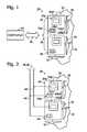
- FIG. 1is a simplified, fragmentary, block/schematic view of a portion of a digitally-addressable, pixelated, fluid-assay, active-matrix micro-structure formed in accordance with a preferred and best mode embodiment of the present invention.
- FIG. 2is similar to FIG. 1 , except that it provides a slightly more detailed view of the structure shown in FIG. 1 .
- FIG. 3which is prepared on a somewhat larger scale than those scales employed in FIGS. 1 and 2 , illustrates, schematically, different, single-matrix organizational ways in which fluid-assay pixels in the matrix micro-structure of this invention may be pre-organized into different functionalized arrangements (different functionalized matrix embodiments) for different fluid-assays that are to be performed.
- FIG. 4is a fragmentary, block/schematic diagram illustrating one form of an electromagnetic field-creating structure (subcomponent) prepared in accordance with practice of the present invention, and specifically such a structure which is intended to create an ambient electromagnetic field environment characterized by light.
- FIG. 5is similar to FIG. 4 , except that it illustrates another field-of-light-environment-creating structure (subcomponent).
- FIG. 6provides a fragmentary, schematic illustration of one form of a heat-field-creating structure (subcomponent).
- FIG. 7illustrates fragmentarily another form of a heat-field-creating structure (subcomponent) which has been prepared on the body of a mechanical cantilever beam which also carries an electrical signaling structure that responds to beam deflection to produce a related electrical output signal.
- FIG. 8is an isometric view of a non-uniform electrical-field-creating structure (subcomponent) prepared through a recently developed process, touched upon later in this specification, involving internal crystalline-structure processing of substrate material.
- FIG. 9provides a simplified side elevation of the structure presented in FIG. 8 , schematically picturing, also, a non-uniform electrical field.
- FIGS. 10A , 10 B and 10 Cillustrate, in greatly simplified forms, three different kinds of three-dimensional spike features which may be created in relation to what is shown generally in FIGS. 8 and 9 for the production of a non-uniform electrical field.
- FIG. 11provides a fragmentary view, somewhat like that presented in FIG. 1 , but here showing a pixel which has been created in accordance with practice of the present invention to include two (plural) assay sensors, each of which hosts a single, fluid-material assay site.
- FIG. 12is somewhat similar to FIG. 11 , except that this figure shows a pixel which has been prepared in accordance with practice of the present invention to include a single fluid-assay sensor which possesses, or hosts, two (plural) fluid-material assay sites.
- active-matrixrefers to a pixelated structure wherein each pixel is controlled by and in relation to some form of digitally-addressable electronic structure, which structure includes digitally-addressable electronic switching structure, defined by one or more electronic switching device(s), operatively associated, as will be seen, with also-included pixel-specific assay-sensor structure and pixel-bathing electromagnetic field-creating structure, also referred to herein as a pixel-internal field source structure—all formed preferably by low-temperature TFT and Si technology as mentioned above.
- bi-alternaterefers to a pre-created matrix condition wherein every other pixel in each row and column of pixels is commonly functionalized to possess response-affinity for one, specific type of a fluid-material assay. This condition effectively creates, across the entire area of the overall matrix of the invention, two differently functionalized submatrices of pixels (what can be thought of as a two-assay, single-matrix condition)
- tri-alternaterefers to a similar condition, but one wherein every third pixel in each row and column has been commonly functionalized for one, specific type of a fluid-material assay. This condition effectively creates, across the entire area of the overall matrix, three, differently functionalized submatrices of pixels (what can be thought of as a three-assay, single-matrix condition). Individual digital addressability of each pixel permits these and other kinds of matrix-distributed functionalization options, if desired.
- FIGS. 1 and 2indicated generally at 20 is a fragmentary portion of a digitally-addressable, pixelated, fluid-assay, active-matrix micro-structure which takes the form herein of a column-and-row array 22 of plural, individually externally digitally-addressable pixels, such as those shown at 24 , 26 , 28 , 30 , 32 , formed, as will shortly be described, on an appropriate supporting substrate 34 made of conventional-material, preferably glass or plastic.
- substrate 34will be considered to be a glass substrate.
- FIGS. 1 and 2are entirely conventional in nature, are well understood by those generally skilled in the relevant art, and thus may easily be practiced in well-known manners to produce the various structural aspects of micro-structure 20 .
- conventional Si-based, thin-film TFT patterning practicessuch as well-known photolithographic practices, may be employed in ways that are familiar to those generally skilled in the art.
- a low-temperature internal crystalline-structure processing approachmay be employed to create certain desired mechanical characteristics, such as the bending characteristics of a cantilever beam like that pictured in FIG.
- various non-critical dimensionsmay be chosen, for example, to define the overall lateral size of a micro-structure, such as micro-structure 20 .
- the number of pixels organized into the relevant, overall row-and-column matrixmay readily be chosen by one practicing the present invention.
- a micro-structure, such as micro-structure 20might have lateral dimensions lying in a range of about 0.4 ⁇ 0.4-inches to about 2 ⁇ 2-inches, and might include an equal row-and-column array of pixels including a total pixel count lying in a range of about 100 to about 10,000.
- a bracket 36 and a double-headed, broad arrow 38represent an appropriate communication/addressing connection, or path, between pixels in micro-structure 20 and a suitable digital computer, such as the computer shown in block form in FIG. 1 at 40 .
- a suitable digital computersuch as the computer shown in block form in FIG. 1 at 40 .
- Such a pathexists and is employed under circumstances where a micro-structure, such as micro-structure 20 , is being (a) functionalized, or (b) “read” after the performance of a fluid-material assay.
- This inclusion of computer 40 in FIG. 1has been done to help illustrate and describe the utility of the present invention.
- each of the mentioned pixelsis essentially identical to each other pixel, although, as will later be explained herein, this is not a necessary requirement of the present invention.
- This “not-necessary” statement regarding the characteristics of the present inventionis based upon a clear understanding that there are various end-result fluid-assay applications with respect to which appropriately functionally differentiated pixels might be fabricated in a single, micro-structure array. Some of these differentiated-pixel concepts will be discussed more fully later herein.
- pixel 24In general terms, and using pixel 24 as an illustration to explain the basic construction of each of the pixels shown in array 22 , included in pixel 24 are several, fully integrated, pixel-specific components, or substructures. These include, as part of more broadly inclusive pixel-specific electronic structure, ( 1 ) thin-film, digitally-addressable electronic switching structure, ( 2 ) a fully assay-functionalized, individually remotely digitally-addressable and accessible assay sensor 24 a which hosts what was once, i.e., before functionalization, a “prospective” , functionalizable assay site 24 a 1 , and ( 3 ) what is referred to herein as a pixel-bathing, ambient environmental, preferably thin-film electromagnetic-field-creating structure 24 b .
- Subcomponent 24 b 1is capable of creating a pixel-bathing light field, subcomponent 24 b 2 a pixel-bathing heat field, and subcomponent 24 b 3 a non-uniform pixel-bathing electrical field. More will be said about these three different kinds of field-creating subcomponents shortly.
- a bathing electromagnetic field of an appropriate selected character during pixel functionalizationoperates to create, within a pixel and adjacent an assay site, an ambient environmental condition wherein relevant chemical, biochemical, etc. reactions regarding functionalization flow material can take place, at least at the prepared, sensor-possessed assay site, or sites, to ensure proper functionalization at that site.
- a “prepared assay site”might typically, i.e., conventionally, be defined by a sensor borne area of plated gold.
- each pixelis appropriately prepared with one or more conventional electronic switching device(s) (part of the mentioned electronic switching structure) relevant to accessing and addressing its included sensor(s) and assay site(s), and its field-creating structure. Illustrations of such switching devices are given later herein.
- FIG. 2indicated generally at 42 , 44 are two different communication line systems which are operatively connected, respectively, to the field-creating structures in the illustrated pixels, and to the assay sensors and assay sites shown in these pixels.
- the upper, fragmented ends of line systems 42 , 44 in FIG. 2are embraced by a bracket marked 36 , 38 , which bracket represents the previously mentioned “path” of operative connection shown to exist in FIG. 1 between micro-structure 20 and computer 40 .
- Line system 42which may at an earlier stage in the life of matrix 20 have been utilized by such a computer to energize field-creating subcomponents during an initial, matrix-completing, functionalization procedure, may also be used to energize these same field-creating subcomponents, where appropriate, during reading-out of the results of a performed assay.
- Line system 44directly couples, on a pixel-by-pixel basis, to computer 40 assay-result output responses derived from functionalized assay sites.
- Regions A, B, C in FIG. 3illustrate three other, representative, possible pixel functionalization patterns (specifically submatrix patterns) accommodated by the utility of the present invention.
- intersecting, solid, horizontal and vertical linessuch as lines 52 , 54 , respectively, and intersecting, dashed, horizontal and vertical lines, such as lines 56 , 58 , respectively, illustrate two, different submatrix functionalization patterns which fit each into the category mentioned earlier herein as a bi-alternate functionalization pattern which effectively creates two, large-area-distribution submatrices within the overall matrix array 22 of pixels.
- These two pixel submatricesare distributed across the entire area of the overall matrix array, and are characterized by rows and columns of pixels which “sit” two pixel spacings away from one another.
- FIG. Cillustrates another submatrix functionalization pattern wherein intersecting, light, solid, horizontal and vertical lines, such as lines 60 , 62 , respectively, intersecting dashed, horizontal and vertical lines, such as lines 64 , 66 , respectively, and intersecting, thickened, solid, horizontal and vertical lines, such as lines 68 , 70 , respectively, represent what was referred to herein earlier as a tri-alternate functionalization arrangement distributed over the entire matrix array 22 of pixels—effectively dividing that array into three overlapping submatrices.
- FIG. 3Those skilled in the art, looking at the illustrative, suggested functionalization patterns illustrated in FIG. 3 , will understand how these, and perhaps other, functionalization patterns interestingly tap the utility of the structure of the present invention. In point of fact, what is shown in FIG. 3 suggests that the nature of this invention offers a large, generous palette of opportunities for employing the micro-structure of this invention.
- FIGS. 4 and 5these two figures illustrate, schematically and fragmentarily, two different kinds of light-field-creating subcomponents. These illustrated subcomponents, with respect to what has been shown and discussed earlier herein regarding FIGS. 1 and 2 , might sit at the field-creating subcomponent location which is labeled 24 b 1 in FIGS. 1 and 2 .
- FIGS. 4 and 5in relation to the appearances of things in FIGS. 1 and 2 , have been drawn somewhat differently for illustration purposes.
- an optical beam device 78having a light output port 78 a , is switched on and off by means of an optical switching device 80 (an electronic switching device) which is fed light through an appropriate optical beam structure 82 which in turn is coupled to an off-pixel source of light. Switching of optical switching device 80 is performed by a computer, such as previously mentioned computer 40 , and via previously mentioned line system 42 .
- a sinuous arrow 84represents a path of light flow to create a field of light in the vicinity of prospective assay site 24 a 1 .
- optical mediaIn each of the possible optical field-creating structures shown in FIGS. 5 and 6 , there are different specific arrangements of optical media, well-known to those skilled in the art, which may be employed herein. For example, one such medium might have a horizontal-style configuration, and another arrangement might be characterized by a vertical-style arrangement. Such arrangements are well-known and understood by those skilled in the relevant art.
- the first-mentioned version of a heat-field-creating subcomponentis shown generally at 86 in FIG. 6 .
- This subcomponent ( 86 )is also labeled 24 b 2 (in FIG. 6 ) in order to indicate its relationship to what has already been discussed above regarding the illustrations provided in FIGS. 1 and 2 .
- From a brief look at the schematic illustration presented in FIG. 6those generally skilled in the relevant art will easily recognize how to fabricate an appropriate, similar heat-field-creating organization. Accordingly, and because of the fact that many different, particular heat-field-creating arrangements may be employed, no specific details for such an arrangement are described or illustrated herein.
- the heat-field-creating subcomponent version illustrated generally at 88 in FIG. 7is one which is shown as having been formed directly adjacent assay site 24 a 1 on a portion of assay sensor 24 a , and specifically, formed directly on the beam 90 a of a cantilever-type micro-deflection device 90 whose basic material body has been formed utilizing the process mentioned above referred to as internal crystalline-structure processing.
- FIGS. 8-10Cillustrate various aspects of an electronically (computer) switchable, non-uniform-electrical-field-creating structure 94 which may be created within a pixel, such as within pixel 24 at the site shown at 24 b 3 in FIGS. 1 and 2 .
- the mechanical spike structures seen in these figureshave been fabricated employing the crystalline-structure-processing methodology described in the above-referred-to '451 B2 U.S. patent.
- FIGS. 10A , 10 B and 10 Cillustrate several, different, representative micro-spike configurations and arrangements which might be used to characterize a non-uniform electrical field-creating subcomponent.
- Such micro-spikesare simply illustrative of one of various kinds of different, electronically (computer) switchable structures which may be created within a field-creating structure in a pixel to develop, when energized, a suitable, non-uniform electrical field.
- FIG. 10Aillustrates modified micro-spike structures 94 a regarding which distributed micro-spikes may have, either uniformly, or differentially, different heights lying within a user-selectable height range generally indicated at H.
- FIG. 10Billustrates an arrangement wherein micro-spikes 94 a are configured like those shown in FIGS. 8 and 9 , except for the fact that these FIG. 10B micro-spikes are more densely organized, as indicated by next-adjacent, interspike distance D.
- Such an interspike distanceis freely chooseable by a user, and need not be uniform throughout a full sub-array of micro-spikes.
- FIG. 10CWhat is illustrated in FIG. 10C is an arrangement wherein the pictured micro-spikes 94 a may have several differentiating characteristics, such as differentiating heights and sharpnesses (i.e., pointednesses).
- FIG. 11is a modified fragmentary region drawn from the fragmentary illustration of FIG. 1 .
- This figurespecifically illustrates a pixel 98 possessing two assay sensors 98 a , 98 b , each of which hosts but a single prospective assay site 98 a 1 , 98 b 1 , respectively.
- FIG. 12shows an arrangement wherein a pixel 100 which possesses a single sensor 100 a is structured so as to host two, different, potential assay sites 100 a 1 and 100 a 2 .
- each pixel in that matrixis originally individually and independently functionalizable to display an affinity for at least one specific fluid-assay material, and following such functionalization, and the subsequent performance of a relevant assay, individually and independently digitally readable to assess assay results.
- Independent digital addressability of each pixelintroduces interesting opportunities (not offered by prior art structures) for conducting fluid-material assays in many new ways, including ways that include examining assay results on kinetic and time-based axes of information.
- a single matrixmay be employed in one-to-many fluid-material assays.
- the matrix structure of the inventionpreferably utilizes a low-cost substrate material, such as glass or plastic, and features the low-temperature fabrication on such a substrate of supported pixel structures, including certain kinds of special internal components or substructures, all formed preferably by low-temperature TFT and Si technology as discussed above.
- a low-cost substrate materialsuch as glass or plastic
- features the low-temperature fabrication on such a substrate of supported pixel structuresincluding certain kinds of special internal components or substructures, all formed preferably by low-temperature TFT and Si technology as discussed above.
Landscapes
- Chemical & Material Sciences (AREA)
- Health & Medical Sciences (AREA)
- Dispersion Chemistry (AREA)
- Analytical Chemistry (AREA)
- General Health & Medical Sciences (AREA)
- Hematology (AREA)
- Clinical Laboratory Science (AREA)
- Chemical Kinetics & Catalysis (AREA)
- Apparatus Associated With Microorganisms And Enzymes (AREA)
Abstract
Description
Claims (3)
Priority Applications (2)
| Application Number | Priority Date | Filing Date | Title |
|---|---|---|---|
| US11/827,174US8231831B2 (en) | 2006-10-06 | 2007-07-10 | Micro-pixelated fluid-assay structure |
| PCT/JP2007/070021WO2008044779A1 (en) | 2006-10-06 | 2007-10-05 | Micro-pixelated fluid-assay structure, micro-pixelated fluid-assay precursor structure, and making method and performing method thereof |
Applications Claiming Priority (2)
| Application Number | Priority Date | Filing Date | Title |
|---|---|---|---|
| US84987506P | 2006-10-06 | 2006-10-06 | |
| US11/827,174US8231831B2 (en) | 2006-10-06 | 2007-07-10 | Micro-pixelated fluid-assay structure |
Publications (2)
| Publication Number | Publication Date |
|---|---|
| US20080084372A1 US20080084372A1 (en) | 2008-04-10 |
| US8231831B2true US8231831B2 (en) | 2012-07-31 |
Family
ID=39274593
Family Applications (1)
| Application Number | Title | Priority Date | Filing Date |
|---|---|---|---|
| US11/827,174Expired - Fee RelatedUS8231831B2 (en) | 2006-10-06 | 2007-07-10 | Micro-pixelated fluid-assay structure |
Country Status (1)
| Country | Link |
|---|---|
| US (1) | US8231831B2 (en) |
Cited By (34)
| Publication number | Priority date | Publication date | Assignee | Title |
|---|---|---|---|---|
| US20110217697A1 (en)* | 2008-06-25 | 2011-09-08 | Life Technologies Corporation | Methods and apparatus for measuring analytes using large scale fet arrays |
| US20110263463A1 (en)* | 2008-10-22 | 2011-10-27 | Life Technologies Corporation | Integrated sensor arrays for biological and chemical analysis |
| US8415716B2 (en) | 2006-12-14 | 2013-04-09 | Life Technologies Corporation | Chemically sensitive sensors with feedback circuits |
| US8421437B2 (en) | 2010-06-30 | 2013-04-16 | Life Technologies Corporation | Array column integrator |
| US8435395B2 (en) | 2006-12-14 | 2013-05-07 | Life Technologies Corporation | Methods and apparatus for measuring analytes using large scale FET arrays |
| US8492799B2 (en) | 2006-12-14 | 2013-07-23 | Life Technologies Corporation | Methods and apparatus for detecting molecular interactions using FET arrays |
| US8552771B1 (en) | 2012-05-29 | 2013-10-08 | Life Technologies Corporation | System for reducing noise in a chemical sensor array |
| US8592154B2 (en) | 2009-05-29 | 2013-11-26 | Life Technologies Corporation | Methods and apparatus for high speed operation of a chemically-sensitive sensor array |
| US8685324B2 (en) | 2010-09-24 | 2014-04-01 | Life Technologies Corporation | Matched pair transistor circuits |
| US8747748B2 (en) | 2012-01-19 | 2014-06-10 | Life Technologies Corporation | Chemical sensor with conductive cup-shaped sensor surface |
| US8776573B2 (en) | 2009-05-29 | 2014-07-15 | Life Technologies Corporation | Methods and apparatus for measuring analytes |
| US8821798B2 (en) | 2012-01-19 | 2014-09-02 | Life Technologies Corporation | Titanium nitride as sensing layer for microwell structure |
| US8841217B1 (en) | 2013-03-13 | 2014-09-23 | Life Technologies Corporation | Chemical sensor with protruded sensor surface |
| US8858782B2 (en) | 2010-06-30 | 2014-10-14 | Life Technologies Corporation | Ion-sensing charge-accumulation circuits and methods |
| US8963216B2 (en) | 2013-03-13 | 2015-02-24 | Life Technologies Corporation | Chemical sensor with sidewall spacer sensor surface |
| US8962366B2 (en) | 2013-01-28 | 2015-02-24 | Life Technologies Corporation | Self-aligned well structures for low-noise chemical sensors |
| US9080968B2 (en) | 2013-01-04 | 2015-07-14 | Life Technologies Corporation | Methods and systems for point of use removal of sacrificial material |
| US9116117B2 (en) | 2013-03-15 | 2015-08-25 | Life Technologies Corporation | Chemical sensor with sidewall sensor surface |
| US9128044B2 (en) | 2013-03-15 | 2015-09-08 | Life Technologies Corporation | Chemical sensors with consistent sensor surface areas |
| US9618475B2 (en) | 2010-09-15 | 2017-04-11 | Life Technologies Corporation | Methods and apparatus for measuring analytes |
| US9671363B2 (en) | 2013-03-15 | 2017-06-06 | Life Technologies Corporation | Chemical sensor with consistent sensor surface areas |
| US9823217B2 (en) | 2013-03-15 | 2017-11-21 | Life Technologies Corporation | Chemical device with thin conductive element |
| US9835585B2 (en) | 2013-03-15 | 2017-12-05 | Life Technologies Corporation | Chemical sensor with protruded sensor surface |
| US9841398B2 (en) | 2013-01-08 | 2017-12-12 | Life Technologies Corporation | Methods for manufacturing well structures for low-noise chemical sensors |
| US9960253B2 (en) | 2010-07-03 | 2018-05-01 | Life Technologies Corporation | Chemically sensitive sensor with lightly doped drains |
| US9970984B2 (en) | 2011-12-01 | 2018-05-15 | Life Technologies Corporation | Method and apparatus for identifying defects in a chemical sensor array |
| US10077472B2 (en) | 2014-12-18 | 2018-09-18 | Life Technologies Corporation | High data rate integrated circuit with power management |
| US10100357B2 (en) | 2013-05-09 | 2018-10-16 | Life Technologies Corporation | Windowed sequencing |
| US10379079B2 (en) | 2014-12-18 | 2019-08-13 | Life Technologies Corporation | Methods and apparatus for measuring analytes using large scale FET arrays |
| US10451585B2 (en) | 2009-05-29 | 2019-10-22 | Life Technologies Corporation | Methods and apparatus for measuring analytes |
| US10458942B2 (en) | 2013-06-10 | 2019-10-29 | Life Technologies Corporation | Chemical sensor array having multiple sensors per well |
| US10605767B2 (en) | 2014-12-18 | 2020-03-31 | Life Technologies Corporation | High data rate integrated circuit with transmitter configuration |
| US11307166B2 (en) | 2010-07-01 | 2022-04-19 | Life Technologies Corporation | Column ADC |
| US11339430B2 (en) | 2007-07-10 | 2022-05-24 | Life Technologies Corporation | Methods and apparatus for measuring analytes using large scale FET arrays |
Citations (23)
| Publication number | Priority date | Publication date | Assignee | Title |
|---|---|---|---|---|
| WO1992010092A1 (en) | 1990-12-06 | 1992-06-25 | Affymax Technologies N.V. | Very large scale immobilized polymer synthesis |
| US5143854A (en) | 1989-06-07 | 1992-09-01 | Affymax Technologies N.V. | Large scale photolithographic solid phase synthesis of polypeptides and receptor binding screening thereof |
| US5514501A (en) | 1994-06-07 | 1996-05-07 | The United States Of America As Represented By The Secretary Of Commerce | Process for UV-photopatterning of thiolate monolayers self-assembled on gold, silver and other substrates |
| US6093302A (en) | 1998-01-05 | 2000-07-25 | Combimatrix Corporation | Electrochemical solid phase synthesis |
| US6197503B1 (en) | 1997-11-26 | 2001-03-06 | Ut-Battelle, Llc | Integrated circuit biochip microsystem containing lens |
| US6403317B1 (en)* | 1999-03-26 | 2002-06-11 | Affymetrix, Inc. | Electronic detection of hybridization on nucleic acid arrays |
| US20030035109A1 (en) | 2000-03-17 | 2003-02-20 | Gerhard Hartwich | Device and method for detecting organic molecules in a test substance |
| US6551784B2 (en) | 1989-06-07 | 2003-04-22 | Affymetrix Inc | Method of comparing nucleic acid sequences |
| US6605796B2 (en) | 2000-05-25 | 2003-08-12 | Westar Photonics | Laser beam shaping device and apparatus for material machining |
| JP2003322613A (en) | 2002-04-30 | 2003-11-14 | Omron Corp | Optical device, specimen mounting component, measuring method, analytical system, person collation method and allergy and side-effect inspection method |
| US20030219196A1 (en)* | 2002-05-22 | 2003-11-27 | Tsu-Chien Weng | Microarray system and method of use thereof |
| JP2004001200A (en) | 2002-04-23 | 2004-01-08 | Sharp Corp | Crystallized mechanical device, its method and its manufacturing system |
| US6794052B2 (en) | 1994-10-18 | 2004-09-21 | The Regents Of The University Of California | Polymer arrays from the combinatorial synthesis of novel materials |
| US6860939B2 (en)* | 2002-04-23 | 2005-03-01 | Sharp Laboratories Of America, Inc. | Semiconductor crystal-structure-processed mechanical devices, and methods and systems for making |
| US20050063870A1 (en)* | 2003-09-01 | 2005-03-24 | Seiko Epson Corporation | Biosensor and method of manufacturing biosensor |
| US6985655B2 (en) | 2002-01-30 | 2006-01-10 | Affymetrix, Inc. | Compositions and methods involving direct write optical lithography |
| JP2006017706A (en) | 2005-06-14 | 2006-01-19 | Hayashi Soken:Kk | Biochip on-line analytical system |
| JP2006504111A (en) | 2002-10-22 | 2006-02-02 | ユニヴァーシティー カレッジ カーディフ コンサルタンツ リミテッド | Semiconductor optical device |
| US7128783B2 (en) | 2002-04-23 | 2006-10-31 | Sharp Laboratories Of America, Inc. | Thin-film crystal-structure-processed mechanical devices, and methods and systems for making |
| US7135070B2 (en) | 2002-04-23 | 2006-11-14 | Sharp Laboratories Of America, Inc. | Monolithic stacked/layered crystal-structure-processed mechanical, and combined mechanical and electrical, devices and methods and systems for making |
| US7156916B2 (en) | 2002-04-23 | 2007-01-02 | Sharp Laboratories Of America, Inc. | Monolithic integrated crystal-structure-processed mechanical, and combined mechanical and electrical devices, and methods and systems for making |
| US7163822B2 (en) | 2002-05-14 | 2007-01-16 | Hitachi, Ltd. | Apparatus and method for luminometric assay |
| US20070072169A1 (en) | 2005-09-29 | 2007-03-29 | Combimatrix Corporation | Process and apparatus for measuring binding events on a microarray of electrodes |
- 2007
- 2007-07-10USUS11/827,174patent/US8231831B2/ennot_activeExpired - Fee Related
Patent Citations (25)
| Publication number | Priority date | Publication date | Assignee | Title |
|---|---|---|---|---|
| US5143854A (en) | 1989-06-07 | 1992-09-01 | Affymax Technologies N.V. | Large scale photolithographic solid phase synthesis of polypeptides and receptor binding screening thereof |
| US6551784B2 (en) | 1989-06-07 | 2003-04-22 | Affymetrix Inc | Method of comparing nucleic acid sequences |
| WO1992010092A1 (en) | 1990-12-06 | 1992-06-25 | Affymax Technologies N.V. | Very large scale immobilized polymer synthesis |
| US5514501A (en) | 1994-06-07 | 1996-05-07 | The United States Of America As Represented By The Secretary Of Commerce | Process for UV-photopatterning of thiolate monolayers self-assembled on gold, silver and other substrates |
| US6794052B2 (en) | 1994-10-18 | 2004-09-21 | The Regents Of The University Of California | Polymer arrays from the combinatorial synthesis of novel materials |
| US6197503B1 (en) | 1997-11-26 | 2001-03-06 | Ut-Battelle, Llc | Integrated circuit biochip microsystem containing lens |
| US6093302A (en) | 1998-01-05 | 2000-07-25 | Combimatrix Corporation | Electrochemical solid phase synthesis |
| US6280595B1 (en) | 1998-01-05 | 2001-08-28 | Combimatrix Corporation | Electrochemical solid phase synthesis |
| US6403317B1 (en)* | 1999-03-26 | 2002-06-11 | Affymetrix, Inc. | Electronic detection of hybridization on nucleic acid arrays |
| US20030035109A1 (en) | 2000-03-17 | 2003-02-20 | Gerhard Hartwich | Device and method for detecting organic molecules in a test substance |
| US6605796B2 (en) | 2000-05-25 | 2003-08-12 | Westar Photonics | Laser beam shaping device and apparatus for material machining |
| US6985655B2 (en) | 2002-01-30 | 2006-01-10 | Affymetrix, Inc. | Compositions and methods involving direct write optical lithography |
| JP2004001200A (en) | 2002-04-23 | 2004-01-08 | Sharp Corp | Crystallized mechanical device, its method and its manufacturing system |
| US6860939B2 (en)* | 2002-04-23 | 2005-03-01 | Sharp Laboratories Of America, Inc. | Semiconductor crystal-structure-processed mechanical devices, and methods and systems for making |
| US7125451B2 (en) | 2002-04-23 | 2006-10-24 | Sharp Laboratories Of America, Inc. | Crystal-structure-processed mechanical devices and methods and systems for making |
| US7128783B2 (en) | 2002-04-23 | 2006-10-31 | Sharp Laboratories Of America, Inc. | Thin-film crystal-structure-processed mechanical devices, and methods and systems for making |
| US7135070B2 (en) | 2002-04-23 | 2006-11-14 | Sharp Laboratories Of America, Inc. | Monolithic stacked/layered crystal-structure-processed mechanical, and combined mechanical and electrical, devices and methods and systems for making |
| US7156916B2 (en) | 2002-04-23 | 2007-01-02 | Sharp Laboratories Of America, Inc. | Monolithic integrated crystal-structure-processed mechanical, and combined mechanical and electrical devices, and methods and systems for making |
| JP2003322613A (en) | 2002-04-30 | 2003-11-14 | Omron Corp | Optical device, specimen mounting component, measuring method, analytical system, person collation method and allergy and side-effect inspection method |
| US7163822B2 (en) | 2002-05-14 | 2007-01-16 | Hitachi, Ltd. | Apparatus and method for luminometric assay |
| US20030219196A1 (en)* | 2002-05-22 | 2003-11-27 | Tsu-Chien Weng | Microarray system and method of use thereof |
| JP2006504111A (en) | 2002-10-22 | 2006-02-02 | ユニヴァーシティー カレッジ カーディフ コンサルタンツ リミテッド | Semiconductor optical device |
| US20050063870A1 (en)* | 2003-09-01 | 2005-03-24 | Seiko Epson Corporation | Biosensor and method of manufacturing biosensor |
| JP2006017706A (en) | 2005-06-14 | 2006-01-19 | Hayashi Soken:Kk | Biochip on-line analytical system |
| US20070072169A1 (en) | 2005-09-29 | 2007-03-29 | Combimatrix Corporation | Process and apparatus for measuring binding events on a microarray of electrodes |
Non-Patent Citations (18)
| Title |
|---|
| Arntz et al. 2003. "Label-free protein assay based on a nanomechanical cantilever array." Nanotechnology. 14:86-90 (5 pp). |
| Jacobson et al. 1985. "Functionalized Congeners of Adenosine: Preparation of Analogues with High Affinity for A1-Adenosine Receptors" J. Med. Chem. 28:1341 (1 p, abstract only). |
| McGall, et al., Jun. 4, 1997, Journal of the American Chemical Society, 119(22). |
| Noda et al. "Development of Photolithography System with Liquid Crystal Device as Active Mask for Synthesizing DNA Chips", Proceedings of the Japan Society of Mechanical Engineers, Kanto Branch, the Japan Society for Precision Engineering, Ibaraki Conference, 2003, vol. 2003, p. 201-202. Japan. |
| USPTO Office Action, U.S. Appl. No. 11/827,173, dated Apr. 8, 2011, 11 pages total. |
| USPTO Office Action, U.S. Appl. No. 11/827,173, dated Dec. 8, 2010, 10 pages total. |
| USPTO Office Action, U.S. Appl. No. 11/827,173, dated May 21, 2010, 9 pages total. |
| USPTO Office Action, U.S. Appl. No. 11/827,173, dated Nov. 27, 2009, 14 pages total. |
| USPTO Office Action, U.S. Appl. No. 11/827,175, dated Jan. 3, 2011, 13 pages total. |
| USPTO Office Action, U.S. Appl. No. 11/827,175, dated May 31, 2011, 11 pages total. |
| USPTO Office Action, U.S. Appl. No. 11/827,176, dated Jan. 3, 2011, 14 pages total. |
| USPTO Office Action, U.S. Appl. No. 11/827,176, dated May 31, 2011, 10 pages total. |
| USPTO Office Action, U.S. Appl. No. 11/827,335, dated Apr. 12, 2011, 13 pages total. |
| USPTO Office Action, U.S. Appl. No. 11/827,335, dated Aug. 11, 2010, 16 pages total. |
| USPTO Office Action, U.S. Appl. No. 11/827,335, dated Mar. 15, 2010, 20 pages total. |
| USPTO Office Action, U.S. Appl. No. 11/888,491, dated Apr. 12, 2011, 11 pages total. |
| USPTO Office Action, U.S. Appl. No. 11/888,491, dated Jun. 25, 2010, 11 pages total. |
| USPTO Office Action, U.S. Appl. No. 11/888,491, dated Nov. 15, 2010, 8 pages total. |
Cited By (136)
| Publication number | Priority date | Publication date | Assignee | Title |
|---|---|---|---|---|
| US8540868B2 (en) | 2006-12-14 | 2013-09-24 | Life Technologies Corporation | Methods and apparatus for detecting molecular interactions using FET arrays |
| US8492799B2 (en) | 2006-12-14 | 2013-07-23 | Life Technologies Corporation | Methods and apparatus for detecting molecular interactions using FET arrays |
| US8415716B2 (en) | 2006-12-14 | 2013-04-09 | Life Technologies Corporation | Chemically sensitive sensors with feedback circuits |
| US12066399B2 (en) | 2006-12-14 | 2024-08-20 | Life Technologies Corporation | Methods and apparatus for measuring analytes using large scale FET arrays |
| US8426899B2 (en) | 2006-12-14 | 2013-04-23 | Life Technologies Corporation | Methods and apparatus for measuring analytes using large scale FET arrays |
| US8426898B2 (en) | 2006-12-14 | 2013-04-23 | Life Technologies Corporation | Methods and apparatus for measuring analytes using large scale FET arrays |
| US11732297B2 (en)* | 2006-12-14 | 2023-08-22 | Life Technologies Corporation | Methods and apparatus for measuring analytes using large scale FET arrays |
| US20220340965A1 (en)* | 2006-12-14 | 2022-10-27 | Life Technologies Corporation | Methods and Apparatus for Measuring Analytes Using Large Scale FET Arrays |
| US8435395B2 (en) | 2006-12-14 | 2013-05-07 | Life Technologies Corporation | Methods and apparatus for measuring analytes using large scale FET arrays |
| US8441044B2 (en) | 2006-12-14 | 2013-05-14 | Life Technologies Corporation | Methods for manufacturing low noise chemically-sensitive field effect transistors |
| US8445945B2 (en) | 2006-12-14 | 2013-05-21 | Life Technologies Corporation | Low noise chemically-sensitive field effect transistors |
| US8450781B2 (en) | 2006-12-14 | 2013-05-28 | Life Technologies Corporation | Methods and apparatus for measuring analytes using large scale FET arrays |
| US11435314B2 (en) | 2006-12-14 | 2022-09-06 | Life Technologies Corporation | Chemically-sensitive sensor array device |
| US8540865B2 (en) | 2006-12-14 | 2013-09-24 | Life Technologies Corporation | Methods and apparatus for detecting molecular interactions using FET arrays |
| US8492800B2 (en) | 2006-12-14 | 2013-07-23 | Life Technologies Corporation | Chemically sensitive sensors with sample and hold capacitors |
| US8540866B2 (en) | 2006-12-14 | 2013-09-24 | Life Technologies Corporation | Methods and apparatus for detecting molecular interactions using FET arrays |
| US8496802B2 (en) | 2006-12-14 | 2013-07-30 | Life Technologies Corporation | Methods for operating chemically-sensitive sample and hold sensors |
| US8502278B2 (en) | 2006-12-14 | 2013-08-06 | Life Technologies Corporation | Chemically-sensitive sample and hold sensors |
| US8519448B2 (en) | 2006-12-14 | 2013-08-27 | Life Technologies Corporation | Chemically-sensitive array with active and reference sensors |
| US10816506B2 (en) | 2006-12-14 | 2020-10-27 | Life Technologies Corporation | Method for measuring analytes using large scale chemfet arrays |
| US8530941B2 (en) | 2006-12-14 | 2013-09-10 | Life Technologies Corporation | Methods and apparatus for measuring analytes using large scale FET arrays |
| US8535513B2 (en) | 2006-12-14 | 2013-09-17 | Life Technologies Corporation | Methods and apparatus for measuring analytes using large scale FET arrays |
| US12140560B2 (en) | 2006-12-14 | 2024-11-12 | Life Technologies Corporation | Methods and apparatus for measuring analytes using large scale FET arrays |
| US8890216B2 (en) | 2006-12-14 | 2014-11-18 | Life Technologies Corporation | Methods and apparatus for measuring analytes using large scale FET arrays |
| US8766328B2 (en) | 2006-12-14 | 2014-07-01 | Life Technologies Corporation | Chemically-sensitive sample and hold sensors |
| US8540867B2 (en) | 2006-12-14 | 2013-09-24 | Life Technologies Corporation | Methods and apparatus for detecting molecular interactions using FET arrays |
| US10633699B2 (en) | 2006-12-14 | 2020-04-28 | Life Technologies Corporation | Methods and apparatus for measuring analytes using large scale FET arrays |
| US8558288B2 (en) | 2006-12-14 | 2013-10-15 | Life Technologies Corporation | Methods and apparatus for measuring analytes using large scale FET arrays |
| US8575664B2 (en) | 2006-12-14 | 2013-11-05 | Life Technologies Corporation | Chemically-sensitive sensor array calibration circuitry |
| US10502708B2 (en) | 2006-12-14 | 2019-12-10 | Life Technologies Corporation | Chemically-sensitive sensor array calibration circuitry |
| US10415079B2 (en) | 2006-12-14 | 2019-09-17 | Life Technologies Corporation | Methods and apparatus for detecting molecular interactions using FET arrays |
| US8658017B2 (en) | 2006-12-14 | 2014-02-25 | Life Technologies Corporation | Methods for operating an array of chemically-sensitive sensors |
| US10203300B2 (en) | 2006-12-14 | 2019-02-12 | Life Technologies Corporation | Methods and apparatus for measuring analytes using large scale FET arrays |
| US8685230B2 (en) | 2006-12-14 | 2014-04-01 | Life Technologies Corporation | Methods and apparatus for high-speed operation of a chemically-sensitive sensor array |
| US8692298B2 (en) | 2006-12-14 | 2014-04-08 | Life Technologies Corporation | Chemical sensor array having multiple sensors per well |
| US9989489B2 (en) | 2006-12-14 | 2018-06-05 | Life Technnologies Corporation | Methods for calibrating an array of chemically-sensitive sensors |
| US9951382B2 (en) | 2006-12-14 | 2018-04-24 | Life Technologies Corporation | Methods and apparatus for measuring analytes using large scale FET arrays |
| US9404920B2 (en) | 2006-12-14 | 2016-08-02 | Life Technologies Corporation | Methods and apparatus for detecting molecular interactions using FET arrays |
| US9269708B2 (en) | 2006-12-14 | 2016-02-23 | Life Technologies Corporation | Methods and apparatus for measuring analytes using large scale FET arrays |
| US9134269B2 (en) | 2006-12-14 | 2015-09-15 | Life Technologies Corporation | Methods and apparatus for measuring analytes using large scale FET arrays |
| US8742472B2 (en) | 2006-12-14 | 2014-06-03 | Life Technologies Corporation | Chemically sensitive sensors with sample and hold capacitors |
| US9039888B2 (en) | 2006-12-14 | 2015-05-26 | Life Technologies Corporation | Methods and apparatus for detecting molecular interactions using FET arrays |
| US9023189B2 (en) | 2006-12-14 | 2015-05-05 | Life Technologies Corporation | High density sensor array without wells |
| US8764969B2 (en) | 2006-12-14 | 2014-07-01 | Life Technologies Corporation | Methods for operating chemically sensitive sensors with sample and hold capacitors |
| US11339430B2 (en) | 2007-07-10 | 2022-05-24 | Life Technologies Corporation | Methods and apparatus for measuring analytes using large scale FET arrays |
| US9194000B2 (en) | 2008-06-25 | 2015-11-24 | Life Technologies Corporation | Methods and apparatus for measuring analytes using large scale FET arrays |
| US20110217697A1 (en)* | 2008-06-25 | 2011-09-08 | Life Technologies Corporation | Methods and apparatus for measuring analytes using large scale fet arrays |
| US8470164B2 (en) | 2008-06-25 | 2013-06-25 | Life Technologies Corporation | Methods and apparatus for measuring analytes using large scale FET arrays |
| US8524057B2 (en) | 2008-06-25 | 2013-09-03 | Life Technologies Corporation | Methods and apparatus for measuring analytes using large scale FET arrays |
| US20110263463A1 (en)* | 2008-10-22 | 2011-10-27 | Life Technologies Corporation | Integrated sensor arrays for biological and chemical analysis |
| US11874250B2 (en) | 2008-10-22 | 2024-01-16 | Life Technologies Corporation | Integrated sensor arrays for biological and chemical analysis |
| US11448613B2 (en) | 2008-10-22 | 2022-09-20 | Life Technologies Corporation | ChemFET sensor array including overlying array of wells |
| US11137369B2 (en) | 2008-10-22 | 2021-10-05 | Life Technologies Corporation | Integrated sensor arrays for biological and chemical analysis |
| US12146853B2 (en) | 2008-10-22 | 2024-11-19 | Life Technologies Corporation | Methods and apparatus including array of reaction chambers over array of chemFET sensors for measuring analytes |
| US9944981B2 (en) | 2008-10-22 | 2018-04-17 | Life Technologies Corporation | Methods and apparatus for measuring analytes |
| US9964515B2 (en) | 2008-10-22 | 2018-05-08 | Life Technologies Corporation | Integrated sensor arrays for biological and chemical analysis |
| US8936763B2 (en)* | 2008-10-22 | 2015-01-20 | Life Technologies Corporation | Integrated sensor arrays for biological and chemical analysis |
| US8766327B2 (en) | 2009-05-29 | 2014-07-01 | Life Technologies Corporation | Active chemically-sensitive sensors with in-sensor current sources |
| US8592154B2 (en) | 2009-05-29 | 2013-11-26 | Life Technologies Corporation | Methods and apparatus for high speed operation of a chemically-sensitive sensor array |
| US11692964B2 (en) | 2009-05-29 | 2023-07-04 | Life Technologies Corporation | Methods and apparatus for measuring analytes |
| US8994076B2 (en) | 2009-05-29 | 2015-03-31 | Life Technologies Corporation | Chemically-sensitive field effect transistor based pixel array with protection diodes |
| US8912580B2 (en) | 2009-05-29 | 2014-12-16 | Life Technologies Corporation | Active chemically-sensitive sensors with in-sensor current sources |
| US8748947B2 (en) | 2009-05-29 | 2014-06-10 | Life Technologies Corporation | Active chemically-sensitive sensors with reset switch |
| US11768171B2 (en) | 2009-05-29 | 2023-09-26 | Life Technologies Corporation | Methods and apparatus for measuring analytes |
| US8776573B2 (en) | 2009-05-29 | 2014-07-15 | Life Technologies Corporation | Methods and apparatus for measuring analytes |
| US8698212B2 (en) | 2009-05-29 | 2014-04-15 | Life Technologies Corporation | Active chemically-sensitive sensors |
| US10718733B2 (en) | 2009-05-29 | 2020-07-21 | Life Technologies Corporation | Methods and apparatus for measuring analytes |
| US12038405B2 (en) | 2009-05-29 | 2024-07-16 | Life Technologies Corporation | Methods and apparatus for measuring analytes |
| US8592153B1 (en) | 2009-05-29 | 2013-11-26 | Life Technologies Corporation | Methods for manufacturing high capacitance microwell structures of chemically-sensitive sensors |
| US8822205B2 (en) | 2009-05-29 | 2014-09-02 | Life Technologies Corporation | Active chemically-sensitive sensors with source follower amplifier |
| US9927393B2 (en) | 2009-05-29 | 2018-03-27 | Life Technologies Corporation | Methods and apparatus for measuring analytes |
| US8742469B2 (en) | 2009-05-29 | 2014-06-03 | Life Technologies Corporation | Active chemically-sensitive sensors with correlated double sampling |
| US10451585B2 (en) | 2009-05-29 | 2019-10-22 | Life Technologies Corporation | Methods and apparatus for measuring analytes |
| US10809226B2 (en) | 2009-05-29 | 2020-10-20 | Life Technologies Corporation | Methods and apparatus for measuring analytes |
| US10641729B2 (en) | 2010-06-30 | 2020-05-05 | Life Technologies Corporation | Column ADC |
| US8432149B2 (en) | 2010-06-30 | 2013-04-30 | Life Technologies Corporation | Array column integrator |
| US12038406B2 (en) | 2010-06-30 | 2024-07-16 | Life Technologies Corporation | Semiconductor-based chemical detection device |
| US8742471B2 (en) | 2010-06-30 | 2014-06-03 | Life Technologies Corporation | Chemical sensor array with leakage compensation circuit |
| US8487790B2 (en) | 2010-06-30 | 2013-07-16 | Life Technologies Corporation | Chemical detection circuit including a serializer circuit |
| US10481123B2 (en) | 2010-06-30 | 2019-11-19 | Life Technologies Corporation | Ion-sensing charge-accumulation circuits and methods |
| US9239313B2 (en) | 2010-06-30 | 2016-01-19 | Life Technologies Corporation | Ion-sensing charge-accumulation circuits and methods |
| US9164070B2 (en) | 2010-06-30 | 2015-10-20 | Life Technologies Corporation | Column adc |
| US8731847B2 (en) | 2010-06-30 | 2014-05-20 | Life Technologies Corporation | Array configuration and readout scheme |
| US8432150B2 (en) | 2010-06-30 | 2013-04-30 | Life Technologies Corporation | Methods for operating an array column integrator |
| US8858782B2 (en) | 2010-06-30 | 2014-10-14 | Life Technologies Corporation | Ion-sensing charge-accumulation circuits and methods |
| US8421437B2 (en) | 2010-06-30 | 2013-04-16 | Life Technologies Corporation | Array column integrator |
| US8741680B2 (en) | 2010-06-30 | 2014-06-03 | Life Technologies Corporation | Two-transistor pixel array |
| US8983783B2 (en) | 2010-06-30 | 2015-03-17 | Life Technologies Corporation | Chemical detection device having multiple flow channels |
| US11307166B2 (en) | 2010-07-01 | 2022-04-19 | Life Technologies Corporation | Column ADC |
| US9960253B2 (en) | 2010-07-03 | 2018-05-01 | Life Technologies Corporation | Chemically sensitive sensor with lightly doped drains |
| US12050195B2 (en) | 2010-09-15 | 2024-07-30 | Life Technologies Corporation | Methods and apparatus for measuring analytes using chemfet arrays |
| US9958415B2 (en) | 2010-09-15 | 2018-05-01 | Life Technologies Corporation | ChemFET sensor including floating gate |
| US9958414B2 (en) | 2010-09-15 | 2018-05-01 | Life Technologies Corporation | Apparatus for measuring analytes including chemical sensor array |
| US9618475B2 (en) | 2010-09-15 | 2017-04-11 | Life Technologies Corporation | Methods and apparatus for measuring analytes |
| US8685324B2 (en) | 2010-09-24 | 2014-04-01 | Life Technologies Corporation | Matched pair transistor circuits |
| US8912005B1 (en) | 2010-09-24 | 2014-12-16 | Life Technologies Corporation | Method and system for delta double sampling |
| US9110015B2 (en) | 2010-09-24 | 2015-08-18 | Life Technologies Corporation | Method and system for delta double sampling |
| US8796036B2 (en) | 2010-09-24 | 2014-08-05 | Life Technologies Corporation | Method and system for delta double sampling |
| US10365321B2 (en) | 2011-12-01 | 2019-07-30 | Life Technologies Corporation | Method and apparatus for identifying defects in a chemical sensor array |
| US9970984B2 (en) | 2011-12-01 | 2018-05-15 | Life Technologies Corporation | Method and apparatus for identifying defects in a chemical sensor array |
| US10598723B2 (en) | 2011-12-01 | 2020-03-24 | Life Technologies Corporation | Method and apparatus for identifying defects in a chemical sensor array |
| US8747748B2 (en) | 2012-01-19 | 2014-06-10 | Life Technologies Corporation | Chemical sensor with conductive cup-shaped sensor surface |
| US8821798B2 (en) | 2012-01-19 | 2014-09-02 | Life Technologies Corporation | Titanium nitride as sensing layer for microwell structure |
| US10404249B2 (en) | 2012-05-29 | 2019-09-03 | Life Technologies Corporation | System for reducing noise in a chemical sensor array |
| US9985624B2 (en) | 2012-05-29 | 2018-05-29 | Life Technologies Corporation | System for reducing noise in a chemical sensor array |
| US8552771B1 (en) | 2012-05-29 | 2013-10-08 | Life Technologies Corporation | System for reducing noise in a chemical sensor array |
| US9270264B2 (en) | 2012-05-29 | 2016-02-23 | Life Technologies Corporation | System for reducing noise in a chemical sensor array |
| US8786331B2 (en) | 2012-05-29 | 2014-07-22 | Life Technologies Corporation | System for reducing noise in a chemical sensor array |
| US9852919B2 (en) | 2013-01-04 | 2017-12-26 | Life Technologies Corporation | Methods and systems for point of use removal of sacrificial material |
| US9080968B2 (en) | 2013-01-04 | 2015-07-14 | Life Technologies Corporation | Methods and systems for point of use removal of sacrificial material |
| US10436742B2 (en) | 2013-01-08 | 2019-10-08 | Life Technologies Corporation | Methods for manufacturing well structures for low-noise chemical sensors |
| US9841398B2 (en) | 2013-01-08 | 2017-12-12 | Life Technologies Corporation | Methods for manufacturing well structures for low-noise chemical sensors |
| US8962366B2 (en) | 2013-01-28 | 2015-02-24 | Life Technologies Corporation | Self-aligned well structures for low-noise chemical sensors |
| US9995708B2 (en) | 2013-03-13 | 2018-06-12 | Life Technologies Corporation | Chemical sensor with sidewall spacer sensor surface |
| US8963216B2 (en) | 2013-03-13 | 2015-02-24 | Life Technologies Corporation | Chemical sensor with sidewall spacer sensor surface |
| US8841217B1 (en) | 2013-03-13 | 2014-09-23 | Life Technologies Corporation | Chemical sensor with protruded sensor surface |
| US9823217B2 (en) | 2013-03-15 | 2017-11-21 | Life Technologies Corporation | Chemical device with thin conductive element |
| US9835585B2 (en) | 2013-03-15 | 2017-12-05 | Life Technologies Corporation | Chemical sensor with protruded sensor surface |
| US9116117B2 (en) | 2013-03-15 | 2015-08-25 | Life Technologies Corporation | Chemical sensor with sidewall sensor surface |
| US10481124B2 (en) | 2013-03-15 | 2019-11-19 | Life Technologies Corporation | Chemical device with thin conductive element |
| US9128044B2 (en) | 2013-03-15 | 2015-09-08 | Life Technologies Corporation | Chemical sensors with consistent sensor surface areas |
| US10422767B2 (en) | 2013-03-15 | 2019-09-24 | Life Technologies Corporation | Chemical sensor with consistent sensor surface areas |
| US9671363B2 (en) | 2013-03-15 | 2017-06-06 | Life Technologies Corporation | Chemical sensor with consistent sensor surface areas |
| US10100357B2 (en) | 2013-05-09 | 2018-10-16 | Life Technologies Corporation | Windowed sequencing |
| US10655175B2 (en) | 2013-05-09 | 2020-05-19 | Life Technologies Corporation | Windowed sequencing |
| US11028438B2 (en) | 2013-05-09 | 2021-06-08 | Life Technologies Corporation | Windowed sequencing |
| US11774401B2 (en) | 2013-06-10 | 2023-10-03 | Life Technologies Corporation | Chemical sensor array having multiple sensors per well |
| US10816504B2 (en) | 2013-06-10 | 2020-10-27 | Life Technologies Corporation | Chemical sensor array having multiple sensors per well |
| US11499938B2 (en) | 2013-06-10 | 2022-11-15 | Life Technologies Corporation | Chemical sensor array having multiple sensors per well |
| US10458942B2 (en) | 2013-06-10 | 2019-10-29 | Life Technologies Corporation | Chemical sensor array having multiple sensors per well |
| US10379079B2 (en) | 2014-12-18 | 2019-08-13 | Life Technologies Corporation | Methods and apparatus for measuring analytes using large scale FET arrays |
| US10077472B2 (en) | 2014-12-18 | 2018-09-18 | Life Technologies Corporation | High data rate integrated circuit with power management |
| US11536688B2 (en) | 2014-12-18 | 2022-12-27 | Life Technologies Corporation | High data rate integrated circuit with transmitter configuration |
| US10605767B2 (en) | 2014-12-18 | 2020-03-31 | Life Technologies Corporation | High data rate integrated circuit with transmitter configuration |
| US10767224B2 (en) | 2014-12-18 | 2020-09-08 | Life Technologies Corporation | High data rate integrated circuit with power management |
| US12196704B2 (en) | 2014-12-18 | 2025-01-14 | Life Technologies Corporation | High data rate integrated circuit with transmitter configuration |
Also Published As
| Publication number | Publication date |
|---|---|
| US20080084372A1 (en) | 2008-04-10 |
Similar Documents
| Publication | Publication Date | Title |
|---|---|---|
| US8231831B2 (en) | Micro-pixelated fluid-assay structure | |
| US7763947B2 (en) | Piezo-diode cantilever MEMS | |
| US20080079663A1 (en) | Micro-pixelated fluid-assay precursor structure | |
| DE102017124110B4 (en) | BIO-MOSFETS WITH A COMMON SENSOR TUB | |
| CN101641150B (en) | Integrated microfluidic device with reduced peak power | |
| CN115007233A (en) | Digital microfluidic device including dual substrates with thin film transistors and capacitive sensing | |
| ES2294389T3 (en) | MICROFLUIDIC ARTICLE. | |
| CN109234158B (en) | Biochip and its manufacturing method, operating method, and biological detection system | |
| EP3688464A2 (en) | Nanopore device and method of manufacturing same | |
| JP2004510130A5 (en) | ||
| JP2009531704A (en) | Integrated device comprising an array of photodetectors and an array of sample sites | |
| TW202117854A (en) | Semiconductor device with biofet and biometric sensors | |
| US20120245049A1 (en) | System and Method for Pixelated Fluid Assay | |
| US8236245B2 (en) | Micro-pixelated fluid-assay precursor structure | |
| US8232108B2 (en) | Method of making micro-pixelated fluid-assay structure | |
| JP2004125706A (en) | Method for detecting intereaction, bioassay device, and bioassay substrate | |
| US8236571B2 (en) | Method of making micro-pixelated fluid-assay precursor structure | |
| US8236244B2 (en) | Micro-pixelated fluid-assay structure with on-board addressable, pixel-specific functionalization | |
| KR20110064754A (en) | Microarray Chip and Manufacturing Method Thereof | |
| CN100578222C (en) | A kind of agarose gel plastic substrate and its preparation method and application | |
| KR100298415B1 (en) | apparatus for forming a pattern and method for forming the pattern using the same | |
| US20240238781A1 (en) | Digital Microfluidics Chip and Drive Method thereof, and Digital Microfluidics Apparatus | |
| WO2008044779A1 (en) | Micro-pixelated fluid-assay structure, micro-pixelated fluid-assay precursor structure, and making method and performing method thereof | |
| JP4426968B2 (en) | Method and apparatus for disposing a liquid reaction component on the surface of a substrate to detect a target material by reaction between a plurality of components on the substrate, and an article for use in this method | |
| JP3897265B2 (en) | Method and apparatus for immobilizing a substance on the surface of a measuring chip |
Legal Events
| Date | Code | Title | Description |
|---|---|---|---|
| AS | Assignment | Owner name:SHARP LABORATORIES OF AMERICA, INC., WASHINGTON Free format text:ASSIGNMENT OF ASSIGNORS INTEREST;ASSIGNORS:HARTZELL, JOHN W.;JOSHI, POORAN C.;SCHUELE, PAUL J.;REEL/FRAME:019595/0653 Effective date:20070710 | |
| STCF | Information on status: patent grant | Free format text:PATENTED CASE | |
| AS | Assignment | Owner name:SHARP KABUSHIKI KAISHA, JAPAN Free format text:ASSIGNMENT OF ASSIGNORS INTEREST;ASSIGNOR:SHARP LABORATORIES OF AMERICA INC.;REEL/FRAME:028862/0277 Effective date:20120822 | |
| CC | Certificate of correction | ||
| FEPP | Fee payment procedure | Free format text:PAYOR NUMBER ASSIGNED (ORIGINAL EVENT CODE: ASPN); ENTITY STATUS OF PATENT OWNER: LARGE ENTITY | |
| FPAY | Fee payment | Year of fee payment:4 | |
| FEPP | Fee payment procedure | Free format text:MAINTENANCE FEE REMINDER MAILED (ORIGINAL EVENT CODE: REM.); ENTITY STATUS OF PATENT OWNER: LARGE ENTITY | |
| LAPS | Lapse for failure to pay maintenance fees | Free format text:PATENT EXPIRED FOR FAILURE TO PAY MAINTENANCE FEES (ORIGINAL EVENT CODE: EXP.); ENTITY STATUS OF PATENT OWNER: LARGE ENTITY | |
| STCH | Information on status: patent discontinuation | Free format text:PATENT EXPIRED DUE TO NONPAYMENT OF MAINTENANCE FEES UNDER 37 CFR 1.362 | |
| FP | Lapsed due to failure to pay maintenance fee | Effective date:20200731 |