US8230174B2 - Multi-queue address generator for start and end addresses in a multi-queue first-in first-out memory system - Google Patents
Multi-queue address generator for start and end addresses in a multi-queue first-in first-out memory systemDownload PDFInfo
- Publication number
- US8230174B2 US8230174B2US11/040,926US4092605AUS8230174B2US 8230174 B2US8230174 B2US 8230174B2US 4092605 AUS4092605 AUS 4092605AUS 8230174 B2US8230174 B2US 8230174B2
- Authority
- US
- United States
- Prior art keywords
- queue
- memory system
- queues
- value
- address
- Prior art date
- Legal status (The legal status is an assumption and is not a legal conclusion. Google has not performed a legal analysis and makes no representation as to the accuracy of the status listed.)
- Active, expires
Links
Images


Classifications
- G—PHYSICS
- G06—COMPUTING OR CALCULATING; COUNTING
- G06F—ELECTRIC DIGITAL DATA PROCESSING
- G06F5/00—Methods or arrangements for data conversion without changing the order or content of the data handled
- G06F5/06—Methods or arrangements for data conversion without changing the order or content of the data handled for changing the speed of data flow, i.e. speed regularising or timing, e.g. delay lines, FIFO buffers; over- or underrun control therefor
- G06F5/065—Partitioned buffers, e.g. allowing multiple independent queues, bidirectional FIFO's
Definitions
- the present applicationis related to, and incorporates by reference, U.S. Provisional Patent Application Ser. No. 60/591,499 filed by Mario Au, Jason Z. Mo, Xiaoping Fang, Hui Su, Cheng-Han Wu, Ta-Chung Ma and Lan Lin on Jul. 26, 2004.
- the present applicationis also related to, and incorporates by reference, U.S. Provisional Patent Application Ser. No. 60/600,347 filed by Mario Au, Jason Z. Mo, Xiaoping Fang, Hui Su, Cheng-Han Wu, Ta-Chung Ma and Lan Lin on Aug. 9, 2004.
- the present inventionrelates to a multi-queue first in, first out (FIFO) memory.
- a conventional multi-queue FIFO memory systemtypically includes a large memory, which is logically partitioned into a plurality of queues during the initialization of the system.
- Conventional multi-queue FIFO memory systemsuse programming software on a remote device to generate a bit stream that identifies all of the queue start and end addresses and selects the number of queues to be implemented in the multi-queue FIFO memory system.
- This bit streamis stored in memory external to the multi-queue FIFO memory system, and is re-sent upon initialization of the multi-queue FIFO memory system. There is no local flexibility available to program the FIFO queues.
- the bit streamis sent in a serial fashion to the multi-queue FIFO memory system for configuration.
- the serial bit stream initializationconsumes external programming resources.
- the serial bit stream initializationalso consumes additional logic and time for handshaking logic and communication of the bit stream.
- the queues of a multi-queue FIFO memory systemcan be set to a default setting, wherein the number of queues is set to the maximum number of available queues, and the size of each queue is equal.
- a multi-queue FIFO memory system having a capacity of X Mbytes and having 128 total possible queueswould be set to have 128 queues, each with a capacity of X/128.
- Two pins of the systemare typically dedicated to implementing the default setting, one pin to activate the default mode, and the other pin to enable the default setting.
- the present inventionprovides a multi-queue FIFO memory device that uses existing pins of the device to load a desired number of queues (N) into a queue number register.
- the queue number registeris coupled to a queue size look-up table (LUT), which provides a queue size value in response to the contents of the queue number register.
- the queue size valueindicates the amount of memory (e.g., the number of memory blocks) to be included in each of the N queues.
- the queue size valueis provided to a queue start/end address generator, which automatically generates the start and end address associated with each queue in response to the queue size value. These start and end addresses are stored in queue address register files, which enable proper memory read/write and flag counter operations.
- the programming method of the present inventioncan expanded to simultaneously and independently control the queue programming in more than one multi-queue FIFO memory system.
- FIG. 1is a block diagram of a multi-queue flow-control device in accordance with one embodiment of the present invention.
- FIG. 2is a block diagram of a default parallel programming system 200 in accordance with one embodiment of the present invention.
- FIG. 3is a waveform diagram illustrating the operation of the default parallel programming system of FIG. 2 in accordance with one embodiment of the described invention.
- FIG. 4is a block diagram illustrating the configuration of a queue size look-up table in accordance with one embodiment of the present invention.
- FIG. 5is a block diagram illustrating portions of two multi-queue FIFO systems, which are programmed in accordance with another embodiment of the present invention.
- the present inventionincludes a multi-queue flow-control device, which is implemented on a single chip.
- the multi-queue devicecan be configured to implement between 1 and 128 discrete FIFO queues.
- the userhas full flexibility configuring queues within the device, being able to program the total number of queues between 1 and 128.
- the usercan also independently select the individual queue depths.
- All queues within the devicehave a common data input bus (write port), and a common data output bus (read port).
- Data written to the write portis directed to a respective queue via an internal de-multiplexer, which is addressed by a user.
- Data read from the read portis accessed from a respective queue via an internal multiplexer, addressed by the user.
- Data writes and readscan be performed at high speeds (up to 200 MHz, with access times of 3.6 ns in accordance with one embodiment of the present invention).
- Data write and read operationsare totally independent of each other. Thus, a queue may be selected on the write port, and a different queue may be selected on the read port. Alternately, read and write operations may be selected on the same queue simultaneously.
- the deviceprovides a Full Flag (FF#) and an Empty Flag (EF#) that identify the status of the queues selected for write and read operations, respectively.
- the devicealso provides a Programmable Almost Full Flag (PAF#) and a Programmable Almost Empty Flag (PAE#) that identify the status of the queues selected for write and read operations, respectively.
- the positions of the PAF# and PAE# flagsare programmable by the user.
- the flags for queue Nare specified by the flag name, followed by N (e.g., PAF#_N).
- FIG. 1is a block diagram of a multi-queue flow-control device 100 in accordance with one embodiment of the present invention.
- Device 100includes dual-port memory 101 , write port (de-multiplexer) 110 , write control logic 111 , active write queue flag circuit 114 , output multiplexer 120 , read control logic 121 , active read queue flag circuit 124 , output register 130 and output buffer 131 .
- dual-port memoryis a 4.7 Mbit memory having 512 memory blocks, each with a 9.4 kbit capacity.
- the 4.7 Mbit memorycan be logically divided into up to 128 FIFO queues, each having a minimum capacity of 9 k bits.
- write control logic 111controls write accesses to the various queues in dual-port memory 101 . More specifically, write control logic 111 provides the required control/address signals to input de-multiplexer 110 and dual-port memory 101 in response to a write chip select signal WCS#, a write enable signal WEN#, a write clock signal WCLK, a write address signal WRADD[7:0] and a write address enable signal WADEN. Write control logic 111 also provides control signals to active write queue flag circuit 114 , active read queue flag circuit 124 and read control logic 121 .
- read control logic 121controls read accesses from the various queues in dual-port memory 101 . More specifically, read control logic 121 provides the required control/address signals to output multiplexer 120 and dual-port memory 101 in response to a read chip select signal RCS#, a read enable signal REN#, a read clock signal RCLK, a read address signal RDADD[7:0] and a read address enable signal RADEN. Read control logic 121 also provides control signals to active write queue flag circuit 114 , active read queue flag circuit 124 and write control logic 111 .
- Active write queue flag circuit 114generates a full flag FF# (input ready flag IR#) and programmable almost full flag PAF# in response to the write address WRADD[7:0] and the control signals received by write control logic 111 and read control logic 121 . Also, active read queue flag circuit 124 generates an empty flag EF# (output ready flag OR#) and programmable almost empty flag PAE# in response to the read address RDADD[7:0] and the control signals received by write control logic 111 and read control logic 121 .
- logicis included in the multi-queue FIFO memory system 100 to automatically generate the start and end addresses for each of the queues.
- This logiccan be used to specify any number of queues in the design.
- the number of queuesis written into a local or off-chip memory register. This value is read out upon receipt of a master reset signal.
- a master reset signal and a programming signalare activated, and the desired number of queues is specified using the write queue address signal WRADDR[7:0] or the read queue address signal RDADDR[7:0], which is user selectable.
- the master reset signalis de-activated, the write queue address signal (or the read queue address signal) is latched, thereby storing the desired number of queues.
- the number of queuesis presented to a look up table (LUT) to identify the amount of memory (e.g., the number of memory blocks) to be used in each queue.
- the LUTcan be replaced with a divide function, which divides the total memory capacity (e.g., the total number of memory blocks) by the desired number of queues.
- the start and end addresses of each queueare determined and stored in queue start/end address register files.
- the queue start/end address register files associated with unused queuesstore null values. Initializing the start/end addresses of the queues in the foregoing manner enables proper memory read/write and flag counter operations.
- the present inventionallows for local resetting, thereby saving system resources.
- equal queue depthsare utilized (although this is not necessary).
- a queue start/end address generatorprovides the same range of addresses for each queue.
- the depth of each queueis stored in a memory to be utilized by the queue start/end address generator to determine a variable length queue. This last method can be implemented, for example, by serial programming.
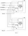
- FIG. 2is a block diagram of a default parallel programming system 200 in accordance with one embodiment of the present invention.
- Default parallel programming system 200includes queue number register 201 , queue size look-up table (LUT) 202 , queue start/end address generator 203 , queue start/end address register files 204 and multiplexer 205 .
- LUTqueue size look-up table
- FIG. 3is a waveform diagram illustrating the operation of default parallel programming system 200 in accordance with the described invention.
- a master reset signal M_RESET# and parallel default programming signal P_PROGare applied to queue number register 201 as illustrated.
- the M_RESET# signalis provided from an existing pin of the multi-queue FIFO device 100 , and therefore does not require any additional pin resources.
- the P_PROG signalPrior to time T 0 , the P_PROG signal is activated high, thereby enabling the default parallel programming mode.
- the M_RESET# signalis activated low, thereby causing the configuration of multi-queue FIFO system 100 to be reset.
- the userPrior to time T 1 , the user provides a queue select signal QS[1:0] having a value of “00” or “11” to the control terminals of multiplexer 205 .
- the queue select signal QS[1:0]has a value of “00”.
- multiplexer 205routes the write address signal WDADDR[7:0] to queue number latch 201 . Note that if the queue select signal QS[1:0] has a value of “11”, then multiplexer 205 routes the read address signal RDADDR[7:0] to queue number latch 201 .
- the usercauses the write address signal WDADDR[7:0] to have a value representative of a user-defined number of queues to be implemented by multi-queue FIFO system 100 .
- the write address signal WDADDR[7:0]is provided from existing pins of the multi-queue FIFO device 100 , and therefore does not require any additional pin resources.
- Multiplexer 205routes the write address signal WDADDR[7:0] to queue number register 201 as the queue number value QNUM.
- the queue number value QNUMhas a value between 0 and 127, inclusive.
- the M_RESET# signaltransitions to a logic “1” value, thereby indicating the end of the master reset operation.
- Queue number register 201latches the QNUM value in response to the rising edge of the M_RESET# signal and the logic high state of the PROG signal.
- Queue number register 201provides the latched queue number value QNUM to queue size LUT 202 .
- Queue size LUT 202stores a default programming configuration for each of the possible queue number values QNUM. More specifically, for each queue number value QNUM (from 0 to 127), queue size LUT 202 stores a corresponding number identifying the amount of memory (e.g., number of memory blocks of the 512 total memory blocks) to be used in each queue.
- FIG. 4is a block diagram illustrating the contents of queue size LUT 202 in accordance with the described embodiment. FIG. 4 illustrates the default size of each queue (in memory blocks) for each of the possible queue number values QNUM.
- queue size LUT 202provides a queue size value equal to 25, thereby indicating that each of the 20 queues should include 25 of the 512 memory blocks.
- Queue size LUT 202provides the number of memory blocks per queue as the queue size value QSIZE.
- Queue start/end address generator 203receives the QSIZE value, and in response, generates the start and end memory addresses for each of the queues. These start and end memory addresses are provided to queue start/end address register files as the Q_SE value.
- queue start/end address generator 203initially provides the 1 st address of the 1 st memory block. This address is stored as the start address of the first queue (i.e., queue 0 ).
- Queue start/end address generator 203then provides the last address of the N th memory block, wherein N is equal to QSIZE.
- queue start/end address generator 203provides the last address of the 25 th memory block. This address is stored as the end address of the first queue (i.e., queue 0 ).
- Queue start/end address generator 203then provides the first address of the (N+1) th memory block (e.g., the 26 th memory block), which is stored as the start address of the second queue (i.e., queue 1 ). Queue start/end address generator 203 then provides the last address of the (2N) th memory block (e.g., the 50 th memory block), which is stored as the end address of the second queue (i.e., queue 1 ). Processing continues in this manner until the start and end addresses of all 20 queues are stored in queue start/end address register files 204 . Note that the start and end addresses of the unused queues 20 - 127 are left as null values in the present example.
- the total number of memory blocksmay not be exactly divisible by the selected number of queues. For example, 20 queues having 25 memory blocks each would result in a total of 500 of the 512 memory blocks being used.
- the left over memory blocksare simply not used.
- the left over memory blocksare added to the last queue. Queue start/end address generator 203 can accomplish this by setting the last address of the last queue equal to the last address of the last memory block.
- FIG. 5is a block diagram illustrating portions of two multi-queue FIFO systems 100 and 500 , which are programmed in accordance with another embodiment of the present invention.
- Multi-queue FIFO system 500is identical to multi-queue FIFO system 100 , and functions to expand the capacity of multi-queue FIFO system 100 .
- Multi-queue FIFO systems 100 and 500are coupled to receive the same master reset signal M_RESET#, the same programming enable signal PROG, the same write address signals WDADDR[7:0] and the same read address signals RDADDR[7:0].
- multi-queue FIFO system 100receives a first queue select signal QS[1:0]
- multi-queue FIFO system 500receives a second queue select signal QS N [1:0].
- the first queue select signal QS[1:0]is selected to have a value of “00”, such that the write address signal WDADDR[7:0] is routed as the queue number value QNUM in multi-queue FIFO system 100 .
- the second queue select signal QS N [1:0]is selected to have a value of “11”, such that the read address signal RDADDR[7:0] is routed as the queue number value QNUM N in multi-queue FIFO system 500 . Consequently, multi-queue FIFO systems 100 and 500 can be simultaneously programmed to have different number of queues.
- multi-queue FIFO system 100is configured to implement 28 queues, each having a capacity of 18 memory blocks. If the read address signal RDADDR[7:0] (i.e., queue number value QNUM N ) has a value of 100, then multi-queue FIFO system 500 is configured to implement 101 queues, each having a capacity of 5 memory blocks.
- the present inventionallows the automatic generation of the queue start and end address locations, given only the desired number of queues.
- the present inventionadvantageously does not require significant additional pin resources.
- the present inventionadvantageously allows the desired number of queues to be communicated to the multi-queue FIFO system 100 in a parallel manner.
- the queue programming method of the present inventioncan be used in combination with conventional programming methods, including, but not limited to, serial bit stream initialization and selecting the maximum number of queues.
- serial bit stream initializationand selecting the maximum number of queues.
Landscapes
- Engineering & Computer Science (AREA)
- Theoretical Computer Science (AREA)
- Physics & Mathematics (AREA)
- General Engineering & Computer Science (AREA)
- General Physics & Mathematics (AREA)
- Multi Processors (AREA)
Abstract
Description
Claims (17)
Priority Applications (1)
| Application Number | Priority Date | Filing Date | Title |
|---|---|---|---|
| US11/040,926US8230174B2 (en) | 2004-07-26 | 2005-01-21 | Multi-queue address generator for start and end addresses in a multi-queue first-in first-out memory system |
Applications Claiming Priority (3)
| Application Number | Priority Date | Filing Date | Title |
|---|---|---|---|
| US59149904P | 2004-07-26 | 2004-07-26 | |
| US60034704P | 2004-08-09 | 2004-08-09 | |
| US11/040,926US8230174B2 (en) | 2004-07-26 | 2005-01-21 | Multi-queue address generator for start and end addresses in a multi-queue first-in first-out memory system |
Publications (2)
| Publication Number | Publication Date |
|---|---|
| US20060020743A1 US20060020743A1 (en) | 2006-01-26 |
| US8230174B2true US8230174B2 (en) | 2012-07-24 |
Family
ID=35658594
Family Applications (1)
| Application Number | Title | Priority Date | Filing Date |
|---|---|---|---|
| US11/040,926Active2030-04-29US8230174B2 (en) | 2004-07-26 | 2005-01-21 | Multi-queue address generator for start and end addresses in a multi-queue first-in first-out memory system |
Country Status (1)
| Country | Link |
|---|---|
| US (1) | US8230174B2 (en) |
Families Citing this family (20)
| Publication number | Priority date | Publication date | Assignee | Title |
|---|---|---|---|---|
| US7447812B1 (en) | 2004-03-23 | 2008-11-04 | Integrated Device Technology, Inc. | Multi-queue FIFO memory devices that support flow-through of write and read counter updates using multi-port flag counter register files |
| US7870310B2 (en)* | 2004-07-26 | 2011-01-11 | Integrated Device Technology, Inc. | Multiple counters to relieve flag restriction in a multi-queue first-in first-out memory system |
| US7523232B2 (en)* | 2004-07-26 | 2009-04-21 | Integrated Device Technology, Inc. | Mark/re-read and mark/re-write operations in a multi-queue first-in first-out memory system |
| US7099231B2 (en)* | 2004-07-26 | 2006-08-29 | Integrated Device Technology, Inc. | Interleaving memory blocks to relieve timing bottleneck in a multi-queue first-in first-out memory system |
| US7257687B2 (en)* | 2004-07-26 | 2007-08-14 | Integrated Device Technology, Inc. | Synchronization of active flag and status bus flags in a multi-queue first-in first-out memory system |
| US7154327B2 (en) | 2004-07-26 | 2006-12-26 | Integrated Device Technology, Inc. | Self-timed multiple blanking for noise suppression during flag generation in a multi-queue first-in first-out memory system |
| US7269700B2 (en)* | 2004-07-26 | 2007-09-11 | Integrated Device Technology, Inc. | Status bus accessing only available quadrants during loop mode operation in a multi-queue first-in first-out memory system |
| US7805552B2 (en)* | 2004-07-26 | 2010-09-28 | Integrated Device Technology, Inc. | Partial packet write and write data filtering in a multi-queue first-in first-out memory system |
| US20060155940A1 (en) | 2005-01-10 | 2006-07-13 | Mario Au | Multi-queue FIFO memory systems that utilize read chip select and device identification codes to control one-at-a-time bus access between selected FIFO memory chips |
| US8255599B2 (en)* | 2006-03-28 | 2012-08-28 | Integrated Device Technology Inc. | Packets transfer device having data absorbing buffers with elastic buffer capacities |
| US20080072113A1 (en)* | 2006-08-30 | 2008-03-20 | Siukwin Tsang | Method of locating packet for resend from retry buffer |
| US7773591B2 (en) | 2007-07-06 | 2010-08-10 | Integrated Device Technology, Inc. | Integrated memory for storing egressing packet data, replay data and to-be egressed data |
| US7852867B2 (en) | 2007-07-06 | 2010-12-14 | Integrated Deoice Technology, Inc. | Integrated memory for storing egressing packet data, replay data and to-be egressed data |
| US8510485B2 (en)* | 2007-08-31 | 2013-08-13 | Apple Inc. | Low power digital interface |
| US7792014B2 (en)* | 2007-09-28 | 2010-09-07 | Integrated Device Technology, Inc. | Method of skipping nullified packets during mass replay from replay buffer |
| US8646383B1 (en) | 2009-09-15 | 2014-02-11 | David Howard | Spiral oven apparatus and method of cooking |
| US8775750B2 (en)* | 2009-09-16 | 2014-07-08 | Nec Corporation | Interleaver with parallel address queue arbitration dependent on which queues are empty |
| US8738860B1 (en)* | 2010-10-25 | 2014-05-27 | Tilera Corporation | Computing in parallel processing environments |
| US10377642B2 (en)* | 2015-11-13 | 2019-08-13 | Bartosz A. Dajnowski | Laser ablation and filtration apparatus and process for removal of hydrocarbons and contaminants |
| CN116821046B (en)* | 2023-08-28 | 2023-11-24 | 上海燧原智能科技有限公司 | Automatic synchronization method, device, equipment and medium for data among heterogeneous units |
Citations (22)
| Publication number | Priority date | Publication date | Assignee | Title |
|---|---|---|---|---|
| US4486854A (en) | 1981-10-15 | 1984-12-04 | Codex Corporation | First-in, first-out memory system |
| US4873666A (en) | 1987-10-14 | 1989-10-10 | Northern Telecom Limited | Message FIFO buffer controller |
| US4888739A (en) | 1988-06-15 | 1989-12-19 | Cypress Semiconductor Corporation | First-in first-out buffer memory with improved status flags |
| US5079693A (en) | 1989-02-28 | 1992-01-07 | Integrated Device Technology, Inc. | Bidirectional FIFO buffer having reread and rewrite means |
| US5600820A (en)* | 1993-12-01 | 1997-02-04 | Bell Communications Research, Inc. | Method for partitioning memory in a high speed network based on the type of service |
| US6044418A (en)* | 1997-06-30 | 2000-03-28 | Sun Microsystems, Inc. | Method and apparatus for dynamically resizing queues utilizing programmable partition pointers |
| US6145061A (en)* | 1998-01-07 | 2000-11-07 | Tandem Computers Incorporated | Method of management of a circular queue for asynchronous access |
| US6381659B2 (en) | 1999-01-19 | 2002-04-30 | Maxtor Corporation | Method and circuit for controlling a first-in-first-out (FIFO) buffer using a bank of FIFO address registers capturing and saving beginning and ending write-pointer addresses |
| US20020080672A1 (en) | 2000-12-26 | 2002-06-27 | Samsung Electronics Co., Ltd. | First-in first-out memory device and method of generating flag signal in the same |
| US20030018862A1 (en) | 2001-07-18 | 2003-01-23 | Karnstedt Curt A. | Integrated circuit FIFO memory devices that are divisible into independent FIFO queues, and systems and methods for controlling same |
| US20030034797A1 (en) | 2001-08-20 | 2003-02-20 | Micron Technology, Inc. | Multi-access fifo queue |
| US6525980B1 (en) | 2001-09-20 | 2003-02-25 | Cypress Semiconductor Corp. | High speed FIFO synchronous programmable full and empty flag generation |
| US6567094B1 (en) | 1999-09-27 | 2003-05-20 | Xerox Corporation | System for controlling read and write streams in a circular FIFO buffer |
| US20030120842A1 (en)* | 2001-08-23 | 2003-06-26 | Bace Matthew M. | Writing and reading data from a queue |
| US6629226B1 (en) | 2000-12-08 | 2003-09-30 | Cypress Semiconductor Corp. | Fifo read interface protocol |
| US6631455B1 (en) | 2000-09-29 | 2003-10-07 | Cypress Semiconductor Corp. | Logic for initializing the depth of the queue pointer memory |
| JP2004139377A (en) | 2002-10-18 | 2004-05-13 | Alps Electric Co Ltd | Fifo circuit |
| US6745264B1 (en)* | 2002-07-15 | 2004-06-01 | Cypress Semiconductor Corp. | Method and apparatus for configuring an interface controller wherein ping pong FIFO segments stores isochronous data and a single circular FIFO stores non-isochronous data |
| US6757679B1 (en)* | 1999-06-25 | 2004-06-29 | International Business Machines Corporation | System for building electronic queue(s) utilizing self organizing units in parallel to permit concurrent queue add and remove operations |
| US6795360B2 (en) | 2001-08-23 | 2004-09-21 | Integrated Device Technology, Inc. | Fifo memory devices that support all four combinations of DDR or SDR write modes with DDR or SDR read modes |
| US6947437B1 (en)* | 2001-05-02 | 2005-09-20 | Advanced Micro Devices, Inc. | Programmable output queues in a network device |
| US7093037B2 (en)* | 2003-09-22 | 2006-08-15 | Emulex Design & Manufacturing Corporation | Generalized queue and specialized register configuration for coordinating communications between tightly coupled processors |
- 2005
- 2005-01-21USUS11/040,926patent/US8230174B2/enactiveActive
Patent Citations (22)
| Publication number | Priority date | Publication date | Assignee | Title |
|---|---|---|---|---|
| US4486854A (en) | 1981-10-15 | 1984-12-04 | Codex Corporation | First-in, first-out memory system |
| US4873666A (en) | 1987-10-14 | 1989-10-10 | Northern Telecom Limited | Message FIFO buffer controller |
| US4888739A (en) | 1988-06-15 | 1989-12-19 | Cypress Semiconductor Corporation | First-in first-out buffer memory with improved status flags |
| US5079693A (en) | 1989-02-28 | 1992-01-07 | Integrated Device Technology, Inc. | Bidirectional FIFO buffer having reread and rewrite means |
| US5600820A (en)* | 1993-12-01 | 1997-02-04 | Bell Communications Research, Inc. | Method for partitioning memory in a high speed network based on the type of service |
| US6044418A (en)* | 1997-06-30 | 2000-03-28 | Sun Microsystems, Inc. | Method and apparatus for dynamically resizing queues utilizing programmable partition pointers |
| US6145061A (en)* | 1998-01-07 | 2000-11-07 | Tandem Computers Incorporated | Method of management of a circular queue for asynchronous access |
| US6381659B2 (en) | 1999-01-19 | 2002-04-30 | Maxtor Corporation | Method and circuit for controlling a first-in-first-out (FIFO) buffer using a bank of FIFO address registers capturing and saving beginning and ending write-pointer addresses |
| US6757679B1 (en)* | 1999-06-25 | 2004-06-29 | International Business Machines Corporation | System for building electronic queue(s) utilizing self organizing units in parallel to permit concurrent queue add and remove operations |
| US6567094B1 (en) | 1999-09-27 | 2003-05-20 | Xerox Corporation | System for controlling read and write streams in a circular FIFO buffer |
| US6631455B1 (en) | 2000-09-29 | 2003-10-07 | Cypress Semiconductor Corp. | Logic for initializing the depth of the queue pointer memory |
| US6629226B1 (en) | 2000-12-08 | 2003-09-30 | Cypress Semiconductor Corp. | Fifo read interface protocol |
| US20020080672A1 (en) | 2000-12-26 | 2002-06-27 | Samsung Electronics Co., Ltd. | First-in first-out memory device and method of generating flag signal in the same |
| US6947437B1 (en)* | 2001-05-02 | 2005-09-20 | Advanced Micro Devices, Inc. | Programmable output queues in a network device |
| US20030018862A1 (en) | 2001-07-18 | 2003-01-23 | Karnstedt Curt A. | Integrated circuit FIFO memory devices that are divisible into independent FIFO queues, and systems and methods for controlling same |
| US20030034797A1 (en) | 2001-08-20 | 2003-02-20 | Micron Technology, Inc. | Multi-access fifo queue |
| US20030120842A1 (en)* | 2001-08-23 | 2003-06-26 | Bace Matthew M. | Writing and reading data from a queue |
| US6795360B2 (en) | 2001-08-23 | 2004-09-21 | Integrated Device Technology, Inc. | Fifo memory devices that support all four combinations of DDR or SDR write modes with DDR or SDR read modes |
| US6525980B1 (en) | 2001-09-20 | 2003-02-25 | Cypress Semiconductor Corp. | High speed FIFO synchronous programmable full and empty flag generation |
| US6745264B1 (en)* | 2002-07-15 | 2004-06-01 | Cypress Semiconductor Corp. | Method and apparatus for configuring an interface controller wherein ping pong FIFO segments stores isochronous data and a single circular FIFO stores non-isochronous data |
| JP2004139377A (en) | 2002-10-18 | 2004-05-13 | Alps Electric Co Ltd | Fifo circuit |
| US7093037B2 (en)* | 2003-09-22 | 2006-08-15 | Emulex Design & Manufacturing Corporation | Generalized queue and specialized register configuration for coordinating communications between tightly coupled processors |
Also Published As
| Publication number | Publication date |
|---|---|
| US20060020743A1 (en) | 2006-01-26 |
Similar Documents
| Publication | Publication Date | Title |
|---|---|---|
| US8230174B2 (en) | Multi-queue address generator for start and end addresses in a multi-queue first-in first-out memory system | |
| US7269700B2 (en) | Status bus accessing only available quadrants during loop mode operation in a multi-queue first-in first-out memory system | |
| US6907479B2 (en) | Integrated circuit FIFO memory devices that are divisible into independent FIFO queues, and systems and methods for controlling same | |
| CN100419667C (en) | FIFO memory device with single data rate and double data rate functions | |
| US7818527B2 (en) | Wrapper circuit and method for interfacing between non-muxed type memory controller and muxed type memory | |
| US6640267B1 (en) | Architecture for multi-queue storage element | |
| US7106098B1 (en) | Split FIFO configuration of block RAM | |
| US8090894B1 (en) | Architectures for supporting communication and access between multiple host devices and one or more common functions | |
| US9478272B1 (en) | Configurable storage blocks with embedded first-in first-out and last-in first-out circuitry | |
| US7257687B2 (en) | Synchronization of active flag and status bus flags in a multi-queue first-in first-out memory system | |
| JPH04301290A (en) | Pushup memory circuit | |
| US7016349B1 (en) | Logic for generating multicast/unicast address (es) | |
| US7035988B1 (en) | Hardware implementation of an N-way dynamic linked list | |
| US7870310B2 (en) | Multiple counters to relieve flag restriction in a multi-queue first-in first-out memory system | |
| US6631455B1 (en) | Logic for initializing the depth of the queue pointer memory | |
| US7099231B2 (en) | Interleaving memory blocks to relieve timing bottleneck in a multi-queue first-in first-out memory system | |
| US7523232B2 (en) | Mark/re-read and mark/re-write operations in a multi-queue first-in first-out memory system | |
| US20030088729A1 (en) | Nonvolatile memory device with double serial/parallel communication interface | |
| JPH11213649A (en) | Pushup memory device | |
| US8806118B2 (en) | Adaptive FIFO | |
| US6925506B1 (en) | Architecture for implementing virtual multiqueue fifos | |
| CN115934004B (en) | Queue management circuit, method, storage device and electronic equipment in the form of linked list | |
| US9837133B1 (en) | Address arithmetic on block RAMs | |
| US7392354B1 (en) | Multi-queue FIFO memory devices that support a backed-off standard mode of operation and methods of operating same | |
| US6625711B1 (en) | Method and/or architecture for implementing queue expansion in multiqueue devices |
Legal Events
| Date | Code | Title | Description |
|---|---|---|---|
| AS | Assignment | Owner name:INTEGRATED DEVICE TECHNOLOGY, INC., CALIFORNIA Free format text:ASSIGNMENT OF ASSIGNORS INTEREST;ASSIGNORS:AU, MARIO;MO, JASON Z.;FANG, XIAOPING;REEL/FRAME:016204/0664 Effective date:20050121 | |
| FEPP | Fee payment procedure | Free format text:PAYOR NUMBER ASSIGNED (ORIGINAL EVENT CODE: ASPN); ENTITY STATUS OF PATENT OWNER: LARGE ENTITY | |
| STCF | Information on status: patent grant | Free format text:PATENTED CASE | |
| FPAY | Fee payment | Year of fee payment:4 | |
| AS | Assignment | Owner name:JPMORGAN CHASE BANK, N.A., AS COLLATERAL AGENT, NE Free format text:SECURITY AGREEMENT;ASSIGNORS:INTEGRATED DEVICE TECHNOLOGY, INC.;GIGPEAK, INC.;MAGNUM SEMICONDUCTOR, INC.;AND OTHERS;REEL/FRAME:042166/0431 Effective date:20170404 Owner name:JPMORGAN CHASE BANK, N.A., AS COLLATERAL AGENT, NEW YORK Free format text:SECURITY AGREEMENT;ASSIGNORS:INTEGRATED DEVICE TECHNOLOGY, INC.;GIGPEAK, INC.;MAGNUM SEMICONDUCTOR, INC.;AND OTHERS;REEL/FRAME:042166/0431 Effective date:20170404 | |
| AS | Assignment | Owner name:INTEGRATED DEVICE TECHNOLOGY, INC., CALIFORNIA Free format text:RELEASE BY SECURED PARTY;ASSIGNOR:JPMORGAN CHASE BANK, N.A.;REEL/FRAME:048746/0001 Effective date:20190329 Owner name:MAGNUM SEMICONDUCTOR, INC., CALIFORNIA Free format text:RELEASE BY SECURED PARTY;ASSIGNOR:JPMORGAN CHASE BANK, N.A.;REEL/FRAME:048746/0001 Effective date:20190329 Owner name:ENDWAVE CORPORATION, CALIFORNIA Free format text:RELEASE BY SECURED PARTY;ASSIGNOR:JPMORGAN CHASE BANK, N.A.;REEL/FRAME:048746/0001 Effective date:20190329 Owner name:CHIPX, INCORPORATED, CALIFORNIA Free format text:RELEASE BY SECURED PARTY;ASSIGNOR:JPMORGAN CHASE BANK, N.A.;REEL/FRAME:048746/0001 Effective date:20190329 Owner name:GIGPEAK, INC., CALIFORNIA Free format text:RELEASE BY SECURED PARTY;ASSIGNOR:JPMORGAN CHASE BANK, N.A.;REEL/FRAME:048746/0001 Effective date:20190329 | |
| MAFP | Maintenance fee payment | Free format text:PAYMENT OF MAINTENANCE FEE, 8TH YEAR, LARGE ENTITY (ORIGINAL EVENT CODE: M1552); ENTITY STATUS OF PATENT OWNER: LARGE ENTITY Year of fee payment:8 | |
| MAFP | Maintenance fee payment | Free format text:PAYMENT OF MAINTENANCE FEE, 12TH YEAR, LARGE ENTITY (ORIGINAL EVENT CODE: M1553); ENTITY STATUS OF PATENT OWNER: LARGE ENTITY Year of fee payment:12 |