US8228730B2 - Memory cell structures and methods - Google Patents
Memory cell structures and methodsDownload PDFInfo
- Publication number
- US8228730B2 US8228730B2US12/872,368US87236810AUS8228730B2US 8228730 B2US8228730 B2US 8228730B2US 87236810 AUS87236810 AUS 87236810AUS 8228730 B2US8228730 B2US 8228730B2
- Authority
- US
- United States
- Prior art keywords
- diode
- memory cell
- insulator
- voltage
- electrode
- Prior art date
- Legal status (The legal status is an assumption and is not a legal conclusion. Google has not performed a legal analysis and makes no representation as to the accuracy of the status listed.)
- Active
Links
- 238000000034methodMethods0.000titleclaimsabstractdescription21
- 239000003989dielectric materialSubstances0.000claimsabstractdescription22
- 239000012212insulatorSubstances0.000claimsdescription55
- 239000000463materialSubstances0.000claimsdescription42
- 230000005641tunnelingEffects0.000claimsdescription15
- 229910021420polycrystalline siliconInorganic materials0.000claimsdescription5
- 229920005591polysiliconPolymers0.000claimsdescription5
- 239000007769metal materialSubstances0.000claimsdescription3
- 239000002159nanocrystalSubstances0.000claimsdescription3
- 239000000758substrateSubstances0.000description15
- 238000010586diagramMethods0.000description11
- VYPSYNLAJGMNEJ-UHFFFAOYSA-NSilicium dioxideChemical compoundO=[Si]=OVYPSYNLAJGMNEJ-UHFFFAOYSA-N0.000description9
- 229910052581Si3N4Inorganic materials0.000description6
- 229910052814silicon oxideInorganic materials0.000description6
- 239000002784hot electronSubstances0.000description5
- 230000005689Fowler Nordheim tunnelingEffects0.000description4
- NRTOMJZYCJJWKI-UHFFFAOYSA-NTitanium nitrideChemical compound[Ti]#NNRTOMJZYCJJWKI-UHFFFAOYSA-N0.000description4
- 230000015556catabolic processEffects0.000description4
- 238000006731degradation reactionMethods0.000description4
- 239000011810insulating materialSubstances0.000description4
- 229910017107AlOxInorganic materials0.000description3
- XUIMIQQOPSSXEZ-UHFFFAOYSA-NSiliconChemical compound[Si]XUIMIQQOPSSXEZ-UHFFFAOYSA-N0.000description3
- -1TaSiSubstances0.000description3
- 229910003134ZrOxInorganic materials0.000description3
- 230000008859changeEffects0.000description3
- 238000002347injectionMethods0.000description3
- 239000007924injectionSubstances0.000description3
- 229910021332silicideInorganic materials0.000description3
- FVBUAEGBCNSCDD-UHFFFAOYSA-Nsilicide(4-)Chemical compound[Si-4]FVBUAEGBCNSCDD-UHFFFAOYSA-N0.000description3
- 229910052710siliconInorganic materials0.000description3
- 239000010703siliconSubstances0.000description3
- 229910052715tantalumInorganic materials0.000description3
- GUVRBAGPIYLISA-UHFFFAOYSA-Ntantalum atomChemical compound[Ta]GUVRBAGPIYLISA-UHFFFAOYSA-N0.000description3
- 229910004200TaSiNInorganic materials0.000description2
- ATJFFYVFTNAWJD-UHFFFAOYSA-NTinChemical compound[Sn]ATJFFYVFTNAWJD-UHFFFAOYSA-N0.000description2
- 229910052751metalInorganic materials0.000description2
- 239000002184metalSubstances0.000description2
- TWNQGVIAIRXVLR-UHFFFAOYSA-Noxo(oxoalumanyloxy)alumaneChemical compoundO=[Al]O[Al]=OTWNQGVIAIRXVLR-UHFFFAOYSA-N0.000description2
- RVTZCBVAJQQJTK-UHFFFAOYSA-Noxygen(2-);zirconium(4+)Chemical compound[O-2].[O-2].[Zr+4]RVTZCBVAJQQJTK-UHFFFAOYSA-N0.000description2
- 239000004065semiconductorSubstances0.000description2
- 239000000377silicon dioxideSubstances0.000description2
- HQVNEWCFYHHQES-UHFFFAOYSA-Nsilicon nitrideChemical compoundN12[Si]34N5[Si]62N3[Si]51N64HQVNEWCFYHHQES-UHFFFAOYSA-N0.000description2
- 229910001928zirconium oxideInorganic materials0.000description2
- 229910003070TaOxInorganic materials0.000description1
- 230000006978adaptationEffects0.000description1
- 238000013459approachMethods0.000description1
- 229910052681coesiteInorganic materials0.000description1
- 239000000470constituentSubstances0.000description1
- 238000010276constructionMethods0.000description1
- 229910052906cristobaliteInorganic materials0.000description1
- 230000001419dependent effectEffects0.000description1
- 230000000694effectsEffects0.000description1
- 230000005669field effectEffects0.000description1
- 230000006870functionEffects0.000description1
- 230000007246mechanismEffects0.000description1
- 150000004767nitridesChemical class0.000description1
- 230000009467reductionEffects0.000description1
- 230000004044responseEffects0.000description1
- 229910052594sapphireInorganic materials0.000description1
- 239000010980sapphireSubstances0.000description1
- 235000012239silicon dioxideNutrition0.000description1
- HWEYZGSCHQNNEH-UHFFFAOYSA-Nsilicon tantalumChemical compound[Si].[Ta]HWEYZGSCHQNNEH-UHFFFAOYSA-N0.000description1
- 229910052682stishoviteInorganic materials0.000description1
- 230000001360synchronised effectEffects0.000description1
- 229910052905tridymiteInorganic materials0.000description1
Images


Classifications
- G—PHYSICS
- G11—INFORMATION STORAGE
- G11C—STATIC STORES
- G11C16/00—Erasable programmable read-only memories
- G11C16/02—Erasable programmable read-only memories electrically programmable
- G11C16/04—Erasable programmable read-only memories electrically programmable using variable threshold transistors, e.g. FAMOS
- G11C16/0408—Erasable programmable read-only memories electrically programmable using variable threshold transistors, e.g. FAMOS comprising cells containing floating gate transistors
- G11C16/0416—Erasable programmable read-only memories electrically programmable using variable threshold transistors, e.g. FAMOS comprising cells containing floating gate transistors comprising cells containing a single floating gate transistor and no select transistor, e.g. UV EPROM
- G—PHYSICS
- G11—INFORMATION STORAGE
- G11C—STATIC STORES
- G11C16/00—Erasable programmable read-only memories
- G11C16/02—Erasable programmable read-only memories electrically programmable
- G11C16/04—Erasable programmable read-only memories electrically programmable using variable threshold transistors, e.g. FAMOS
- G11C16/0483—Erasable programmable read-only memories electrically programmable using variable threshold transistors, e.g. FAMOS comprising cells having several storage transistors connected in series
- H—ELECTRICITY
- H10—SEMICONDUCTOR DEVICES; ELECTRIC SOLID-STATE DEVICES NOT OTHERWISE PROVIDED FOR
- H10B—ELECTRONIC MEMORY DEVICES
- H10B63/00—Resistance change memory devices, e.g. resistive RAM [ReRAM] devices
- H10B63/20—Resistance change memory devices, e.g. resistive RAM [ReRAM] devices comprising selection components having two electrodes, e.g. diodes
- H—ELECTRICITY
- H10—SEMICONDUCTOR DEVICES; ELECTRIC SOLID-STATE DEVICES NOT OTHERWISE PROVIDED FOR
- H10D—INORGANIC ELECTRIC SEMICONDUCTOR DEVICES
- H10D30/00—Field-effect transistors [FET]
- H10D30/60—Insulated-gate field-effect transistors [IGFET]
- H10D30/68—Floating-gate IGFETs
- H10D30/6891—Floating-gate IGFETs characterised by the shapes, relative sizes or dispositions of the floating gate electrode
Definitions
- the present disclosurerelates generally to semiconductor memory devices, methods, and systems, and more particularly, to memory cell structures and methods.
- RAMrandom-access memory
- ROMread only memory
- DRAMdynamic random access memory
- SDRAMsynchronous dynamic random access memory
- PCRAMphase change random access memory
- RRAMresistive random access memory
- MRAMmagnetic random access memory
- STT RAMspin torque transfer random access memory
- Some memory cellscan be 1-transistor (1T) memory cells.
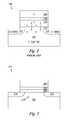
- An example of a flash memory cellis shown in FIG. 1 .
- the flash memory cell 103has a stacked gate structure that includes a floating gate 116 capacitively coupled to a control gate 120 .
- the floating gate 116 and control gate 120are often formed of a polysilicon material and are separated by a dielectric material 118 (e.g., an interpoly dielectric), which can be about 150 to 300 angstroms thick.
- the flash cell 103includes an N+ drain region 112 and an N+ source region 110 inside a well region of a P-substrate 101 .
- the cell 103also includes a tunnel oxide layer 114 overlying a channel region of the substrate 101 (e.g., between the floating gate 116 and the channel region of the substrate 101 ).
- the tunnel oxide layer 114is often silicon dioxide and can be about 70 to 120 angstroms thick.
- the cell 103can be programmed by grounding the source terminal, applying a 5 to 10 volt signal to the drain 112 (e.g., via a bit line not shown), and applying a high programming voltage of, for example, 18 to 20 volts to control gate 120 .
- the high voltage applied to the control gate 120creates a high electric filed across tunnel oxide 114 generating hot electrons in the channel with enough energy to cross the tunnel oxide 114 .
- These hot electronsare then trapped in the floating gate 116 , resulting in a higher threshold voltage for the transistor, which can correspond to the cell 103 being programmed into an OFF (e.g., non-conducting) state.
- the cell 103can be erased by grounding the control gate 120 and the drain region 112 and applying a high voltage (e.g., 18 to 20 volts) to the source region 110 or the P-well region of substrate 101 .
- a high voltagee.g. 18 to 20 volts
- the large voltage differencecauses the trapped electrons on the floating gate 116 to tunnel through the thin oxide layer 114 by a mechanism known as Fowler-Nordheim tunneling.
- 1-transisotor memory cellssuch as flash memory cell 103 have a number of drawbacks with regard to performance.
- the relatively high voltagee.g., 18 to 20V
- the relatively thin tunnel oxide 114can degrade over time (e.g., over multiple program/erase cycles), which can effect the reliability of the cell 103 .
- FIG. 1illustrates a cross-sectional view of a memory cell in accordance with the prior art.
- FIG. 2illustrates a cross-sectional view of a memory cell in accordance with one or more embodiments of the present disclosure.
- FIG. 3Aillustrates a memory cell in an erased state and a programmed state in accordance with one or more embodiments of the present disclosure.
- FIG. 3Bis a diagram illustrating current versus voltage curves corresponding to the memory cell shown in FIG. 3A .
- FIG. 4illustrates a portion of a memory array having one or more memory cells in accordance with embodiments of the present disclosure.
- FIG. 5Ais an energy band diagram corresponding to a diode in accordance with one or more embodiments of the present disclosure.
- FIG. 5Bis a diagram illustrating current density versus voltage associated with the diode of FIG. 5A .
- One or more memory cellsinclude a transistor having a charge storage node, a dielectric material positioned between the charge storage node and a channel region of the transistor, the channel region positioned between a source region and a drain region, and a first electrode of a diode coupled to the charge storage node.
- One or more embodimentsinclude biasing a diode with a first voltage to add charge to a charge storage node of a transistor through the diode, and biasing the diode with a second voltage to remove charge from the charge storage node through the diode.
- a first electrode of the diodeis coupled to the charge storage node. Also, the first voltage and the second voltage are insufficient to provide the tunneling of charge through a dielectric material between the charge storage node and a channel region of the transistor.
- Embodiments of the present disclosureprovide various benefits such as reducing voltages associated with operating (e.g., programming, reading, and/or erasing) memory cells, as compared to previous approaches, among other benefits.
- the reduction in operating voltagescan lead to memory cells having increased scalability and reliability as compared to previous memory cells due to factors such as a reduced tunnel oxide thickness and/or reduced degradation of the tunnel oxide material.
- FIG. 2illustrates a cross-sectional view of a memory cell 211 in accordance with one or more embodiments of the present disclosure.
- the memory cell 211includes a transistor formed in a substrate 201 .
- the substrate 201can be a silicon substrate, silicon on insulator (SOI) substrate, or silicon on sapphire (SOS) substrate, among others.
- the transistorincludes a source region 210 and a drain region 212 , which are separated by a channel region 213 .
- the transistoris formed in a p-type substrate 201 and includes an N+ source region 210 and an N+ drain region 212 ; however, embodiments are not so limited.
- the transistor of memory cell 211includes a dielectric material 222 formed on the substrate 201 and located between the channel region 213 and a charge storage node 224 .
- the dielectric material 222can be a tunnel oxide material (e.g., SiO 2 ) and the storage node 224 can be a floating gate of the transistor.
- the charge storage node 224can be a metal material, a polysilicon material, or a nanocrystal material, among other materials suitable for storing charge.
- the charge storage node 224can be a charge trap flash (CTF).
- the memory cell 211includes a diode 226 having a first electrode (e.g., a bottom electrode) coupled to the charge storage node 224 of the transistor.
- the diode 226can be a metal-insulator diode, in various embodiments.
- Metal-insulator diodescan include one or more insulating materials between the two electrodes of the diode (e.g., between the anode and cathode).
- the diode 226can be a metal-insulator-insulator-metal diode (MIIM diode) or a metal-insulator-insulator-insulator-metal diode (MIIIM).
- the term “metal-insulator diode”includes diodes having one or more insulating materials between the electrodes of the diode. Embodiments are not limited to a particular type of diode 226 .
- the diode 226can be a PIN diode, a Zener diode, a Schottky diode, a resonance tunneling diode (RTD), or a thyristor, in some embodiments.
- a second electrode of the diode 226can be coupled to an access line (e.g., a word line) corresponding to the memory cell 211 , the drain 212 can be coupled to a data/sense line (e.g., a bit line), and the source 210 can be coupled to ground.
- a read voltagecan be applied to the word line and the state of the cell 211 can be determined by sensing current/voltage of the bit line, which is dependent on the Vt of the transistor.
- the 1-transistor memory cell 211does not operate via Fowler-Nordheim tunneling and/or hot electron injection through the dielectric tunnel material 222 .
- embodiments of the present disclosurecan add charge to and/or remove charge from the charge storage node 224 via a conductive path through the diode 226 (e.g., via charge tunneling through the one or more insulator materials of the diode 226 ), rather than through the dielectric material 222 .
- FIG. 3Aillustrates a memory cell in an erased state and a programmed state in accordance with one or more embodiments of the present disclosure.
- the memory cell illustrated in FIG. 3Aincludes a transistor formed in a substrate 301 .
- the transistoris formed in a p-type substrate 301 and includes an N+ source region 310 and an N+ drain region 312 .
- the transistorincludes a dielectric material 322 formed on the substrate 301 and located between the channel region 313 and a charge storage node 324 .
- the charge storage node 324is a floating gate of the transistor.
- the floating gate 324can be a metal material, a polysilicon material, or a nanocrystal material, among other materials suitable for storing charge.
- the memory cell illustrated in FIG. 3Aincludes a diode 326 having a first electrode 327 coupled to the floating gate 324 .
- the diode 326is a metal-insulator diode having an insulator stack 330 positioned between the first electrode 327 and a second electrode 329 .
- the insulator stack 330includes a first insulating material 328 - 1 and a second insulating material 328 - 2 .
- the diode 326is a MIIM diode, in this example.
- FIG. 3Aillustrates the memory cell in an erased state and the right side of FIG. 3A illustrates the memory cell in a programmed state.
- the diode 326can be biased to remove charge (e.g., electrons) from the floating gate 324 through the insulator stack 330 .
- the diode 326can be biased to add charge to the floating gate 324 trough the insulator stack 330 .
- the particular configuration of the diode 326 corresponding to one or more memory cell embodiments of the present disclosurecan depend on various factors such as the current level desired for programming and/or erasing the memory cell, for instance.
- the desired current levelcan depend on factors such as the desired programming time. For instance, to achieve a programming time on the order of nanoseconds (ns) to milliseconds (ms), a current density of about 5 kA/cm 2 to about 5 mA/cm 2 can be used. Embodiments are not limited to a particular programming time and/or current density requirement.
- the current density used to achieve a particular programming/erase timecan depend various factors including the type of material, size, and/or thickness of floating gate 324 , among other factors.
- the diode 326can be an asymmetric MIIM diode such as a tantalum silicide/silicon oxide/zirconium oxide/titanium nitride (TaSi/SiOx/ZrOx/TiN) MIIM diode or a tantalum silicon nitride/silicon oxide/halfnium oxide/titanium nitride (TaSiN/SiOx/HfOx/TiN) MIIM diode.
- asymmetric MIIM diodesuch as a tantalum silicide/silicon oxide/zirconium oxide/titanium nitride (TaSi/SiOx/ZrOx/TiN) MIIM diode or a tantalum silicon nitride/silicon oxide/halfnium oxide/titanium nitride (TaSiN/SiOx/HfOx/TiN) MIIM diode.
- the diode 326can be a symmetric MIIIM diode such as a titanium nitride/silicon nitride/aluminum oxide/halfnium oxide/titanium nitride (TiN/Si 3 N 4 /AlOx/HfOx/TiN) MIIIM diode or a tantalum silicide/silicon nitride/aluminum oxide/zirconium oxide/tantalum silicide (TaSi/Si3N4/AlOx/ZrOx/TaSi) MIIIM diode.
- a symmetric MIIIM diodesuch as a titanium nitride/silicon nitride/aluminum oxide/halfnium oxide/titanium nitride (TiN/Si 3 N 4 /AlOx/HfOx/TiN) MIIIM diode or a tantalum silicide/silicon
- a symmetric dioderefers to a diode having both electrodes of the same material(s) (e.g., such that the work functions of the top/bottom electrodes are the same), while an asymmetric diode includes electrodes made of different materials.
- Electrodesare not limited to these examples.
- various structures for diode 326can produce corresponding current density versus voltage signals suitable for programming, reading, and/or erasing memory cells in accordance with embodiments described herein.
- FIG. 3Bis a diagram illustrating current versus voltage curves corresponding to the memory cell shown in FIG. 3A .
- the diagramillustrates the drain to source current (Ids) versus the voltage (Vd) across the diode 326 .
- Curve 332represents the current versus voltage curve for the cell in the erased state, while curve 333 represents the current versus voltage curve for the cell in the programmed state.
- the state of the memory cellcan be determined by sensing the current Ids responsive to a particular voltage Vd applied to the diode 326 .
- the difference between the curves 332 and 333is due to the different threshold voltage (Vt) of the memory cell depending on whether the cell is programmed (e.g., electrons stored on the floating gate 324 through the insulator stack 330 ) or erased (e.g., electrons removed from floating gate 324 through the insulator stack 330 ).
- Vtthreshold voltage
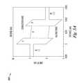
- FIG. 4illustrates a portion of a memory array 400 having one or more memory cells in accordance with embodiments of the present disclosure.
- the embodiment of FIG. 4illustrates an architecture similar to a NAND flash architecture. However, embodiments are not limited to this example.
- the memory array 400includes access lines (e.g., word lines 405 - 1 , 405 - 2 , . . . , 405 -N) and corresponding sense lines (e.g., local bit lines 407 - 1 , 407 - 2 , . . . , 407 -M).
- access linese.g., word lines 405 - 1 , 405 - 2 , . . . , 405 -N
- sense linese.g., local bit lines 407 - 1 , 407 - 2 , . . . , 407 -M.
- bit lines 407 - 1 , 407 - 2 , . . . , 407 -Mcan be some power of two (e.g., 256 word lines by 4,096 bit lines).
- the memory cells 411 - 1 , 411 - 2 , . . . , 411 -N of each NAND string 409 - 1 , 409 - 2 , . . . , 409 -Mare connected in series source to drain between a source select gate (SGS) (e.g., a field-effect transistor (FET) 413 ), and a drain select gate (SGD) (e.g., FET 419 ).
- SGSsource select gate
- FETfield-effect transistor
- SGDdrain select gate
- Each source select gate 413is configured to selectively couple a respective NAND string 409 to a common source 423 responsive to a signal on source select line 417
- each drain select gate 419is configured to selectively couple a respective NAND string 409 to a respective bit line 407 responsive to a signal on drain select line 415 .
- a source of source select gate 413is connected to a common source line 423 .
- the drain of source select gate 413is connected to the source of the memory cell 411 - 1 of the corresponding NAND string 409 - 1 .
- the drain of drain select gate 419is connected to the local bit line 407 - 1 for the corresponding NAND string 409 - 1 at drain contact 421 - 1 .
- the source of drain select gate 419is connected to the drain of the last memory cell 411 -N of the corresponding NAND string 409 - 1 .
- the memory cells 411 - 1 , 411 - 2 , . . . , 411 -Ncan be memory cells such as memory cell 211 illustrated in FIG. 2 .
- construction of memory cells 411 - 1 , 411 - 2 , . . . , 411 -Nincludes a transistor having a source, a drain, a floating gate or other charge storage node 424 , and a diode 426 .
- the diodes 426 of the memory cells 411 - 1 , 411 - 2 , . . . , 411 -Nhave a first electrode coupled to the charge storage node 424 and a second electrode coupled to a respective word line 405 - 1 , 405 - 2 , . . . , 405 -N.
- a “column” of the memory cells 411 - 1 , 411 - 2 , . . . , 411 -Nmake up the NAND strings 409 - 1 , 409 - 2 , . . . , 409 -M and are coupled to a given local bit line 407 - 1 , 407 - 2 , . . . , 407 -M, respectively.
- a “row” of the memory cells 411 - 1 , 411 - 2 , . . . , 411 -Nare those memory cells commonly coupled to a given word line 405 - 1 , 405 - 2 , . . . , 405 -N.
- Operation of the memory array 400can be similar to operation of an array of NAND flash memory cells such as cell 103 described in connection with FIG. 1 .
- a target (e.g., selected) word linee.g., 405 - 1 , 405 - 2 , . . . , 405 -N
- a selected word line associated with the memory cells targeted for the program operationwould receive a first voltage (e.g., a program voltage) designed to change the data state of memory cells coupled to the selected word line if it is not program inhibited (e.g., via an inhibit voltage provided to the bit line to which the memory cell is coupled).
- the program voltage applied to the top electrode of the diode 426is a voltage sufficient to activate (e.g., turn on) the diode 426 to create a conductive path through the diode to add charge to the floating gate 424 .
- the program voltageis insufficient to provide tunneling of electrons through the tunneling dielectric material (e.g., material 222 shown in FIG. 2 or material 322 shown in FIG. 3A ) of the memory cell.
- the program voltagecan have a magnitude of about 3-5 volts.
- the diodes 426 of the memory cells 411 - 1 , 411 - 2 , . . . , 411 -Ncan be biased with an erase voltage opposite in polarity to the programming voltage.
- the erase voltageis sufficient to activate the diode to create a conductive path through the diode 426 to remove charge from the floating gate 422 .
- the erase voltageis insufficient to provide tunneling of electrons through the tunneling dielectric material of the cell.
- the erase voltageis sufficient to create electron tunneling through the insulator material(s) of the diode 426 (e.g., through the insulator stack 330 shown in FIG.
- the erase voltagecan be about 3 to 5 volts, for example. However, the magnitude of the program and/or erase voltage can vary depending on various factors such as the configuration of the diode 426 and the desired programming current and/or desired programming speed, among other factors.
- a sensing operationsuch as a read operation
- conduction of a bit line coupled to a selected cellcan be sensed in order to determine the state of the selected cell.
- the sensing operationcan involve biasing the diode 426 (e.g., via a selected word line 405 - 1 , 405 - 2 , . . . , 405 -N) at a voltage lower in magnitude than the program and/or erase voltage and then sensing voltage and/or current on a bit line (e.g., bit line 407 - 1 ) corresponding to the selected memory cell.
- a read operationcould alternatively include precharging the bit line (e.g., 407 - 1 ) and sensing the discharge with the selected cell begins to conduct.
- the read voltage applied across the diode 426can be about ⁇ 1 to ⁇ 2 volts; however, embodiments are not limited to a particular read voltage.
- the memory cells 411 - 1 , 411 - 2 , . . . , 411 -Ncan be non-volatile memory cells. However, in some embodiments, the memory cells 411 - 1 , 411 - 2 , . . . , 411 -N can be volatile such that power is required to maintain the stored state of the cells.
- FIG. 5Ais an energy band diagram 550 corresponding to a diode in accordance with one or more embodiments of the present disclosure.
- the diagram 550can correspond to a diode such as diode 226 shown in FIG. 2 .
- the diodeis a MIIIM diode that has a stack of three insulator materials (I 1 , I 2 , and I 3 ) between a top electrode (TE) and bottom electrode (BE).
- the top and/or bottom electrodescan be a material such as TaSi, TiN, TaSiN, or a doped polysilicon material.
- the insulator stackcan include various different insulator materials including, but not limited to, various oxide and/or nitride materials such as SiOx, ZrOx, HfOx, AlOx, Si 3 N 4 , TaOx, LaOx, and SiON.
- the insulators I 1 , I 2 , and I 3 of the insulator stackcan have an oxide-nitride-oxide (ONO) configuration.
- At least one of the insulator materials I 1 , I 2 , and I 3can be a high-K dielectric material, in one or more embodiments.
- Embodimentsare not limited to particular diode configuration. For instance, some embodiments can include a diode having more or fewer than three insulator materials in the insulator stack.
- the first (I 1 ) and third (I 3 ) insulatorshave a thickness of about 5 angstroms and the second insulator (I 2 ) has a thickness of about 10 angstroms.
- the dimensions of the insulators I 1 , I 2 , and I 3can vary depending on factors such as the types of insulator materials and the desired current density versus voltage curve, among other factors.
- the energy band diagram 550illustrates the MIIIM diode under reverse bias (e.g., the potential of the top electrode is lower than the potential of the bottom electrode). Under such a reverse bias, electrons can tunnel through the insulator materials of the diode (e.g., from the top electrode to the bottom electrode) and can be stored in a charge storage node (e.g., charge storage node 224 shown in FIG. 2 or floating gate 424 shown in FIG. 4 ), which is coupled to the bottom electrode, as discussed above.
- a charge storage nodee.g., charge storage node 224 shown in FIG. 2 or floating gate 424 shown in FIG. 4
- a forward bias applied across the diodecan be used to induce tunneling of electrons from the charge storage node of the memory cell through the insulator stack in order to remove charge from the storage node (e.g., to erase the memory cell).
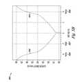
- FIG. 5Bis a diagram 560 illustrating current density versus voltage associated with the diode of FIG. 5A .
- Curve 562represents the metal-insulator diode under reverse bias and curve 564 represents the metal-insulator diode under forward bias.
- the diodeis a symmetric diode such that the forward and reverse bias curves are symmetric; however, embodiments are not limited to this example.
- embodiments of the present disclosurecan include diodes having various asymmetric configurations such that the forward and reverse bias curves would by asymmetric.
- Diagram 560represents one example of a current density versus voltage response of a diode that can be used in accordance with one or more memory cells described herein (e.g., memory cell 211 shown in FIG. 2 ).
- the diodecan be biased at a first voltage (e.g., Vwrite 566 ) in order to program a memory cell.
- the write voltage 566is sufficient to provide a suitable current through the insulator stack of the diode in order to rapidly accumulate charge on the charge storage node of the memory cell.
- Vwrite 566is about ⁇ 4 volts, which provides a current density of about 1 ⁇ 10 6 A/cm 2 .
- the current density associated with programming voltage 566is at least 1 ⁇ 10 4 A/cm 2 .
- the current densitycan vary based on the configuration of the diode and/or the desired programming time for the cell, among other factors.
- the diodecan be biased at a second voltage (e.g., Verase 568 ) in order to erase the memory cell. That is, the erase voltage 568 is sufficient to provide a suitable current through the insulator stack of the diode in order to rapidly remove charge from the charge storage node of the memory cell.
- Verase 568is about 4 volts, which provides a current density of about 1 ⁇ 10 6 A/cm 2 .
- the write voltage (e.g., Vwrite 566 ) and the erase voltage (e.g, Verase 568 )are insufficient to provide the tunneling of charge through a dielectric material (e.g., a tunnel oxide material) between the charge storage node and a channel region of the transistor.
- the erase voltage and the write voltagecan have a magnitude of less than about 5 volts, in some embodiments.
- Biasing the diode with the write voltage 566 and/or the erase voltage 568can include creating a particular voltage difference between the top electrode of the diode and a well region of the substrate. Biasing the diode of the memory cell at a voltage insufficient to promote Fowler-Nordheim tunneling and/or hot electron injection through the tunnel oxide material can prevent degradation of the tunnel oxide material, among other benefits.
- the diodecan be biased with a third voltage (e.g., Vread 567 ).
- the read voltage 567is lower in magnitude than the write voltage 566 and the erase voltage 568 since it is desirable to have a lower current flow through the diode during a read operation.
- the Vread 567is about ⁇ 2 volts, which provides a current density of about 1 ⁇ 10 2 A/cm 2 .
- the current density associated with read voltage 567is not more than 1 ⁇ 10 2 A/cm 2 .
- a logic state(e.g., a logic “0” or “1”) can be determined, for example, by sensing a current between a source and a drain of the transistor responsive to the read voltage applied to the top electrode of the metal-insulator diode.
- One or more memory cellsinclude a transistor having a charge storage node, a dielectric material positioned between the charge storage node and a channel region of the transistor, the channel region positioned between a source region and a drain region, and a first electrode of a diode coupled to the charge storage node.
- One or more embodimentsinclude biasing a diode with a first voltage to add charge to a charge storage node of a transistor through the diode, and biasing the diode with a second voltage to remove charge from the charge storage node through the diode.
- a first electrode of the diodeis coupled to the charge storage node. Also, the first voltage and the second voltage are insufficient to provide the tunneling of charge through a dielectric material between the charge storage node and a channel region of the transistor.
Landscapes
- Engineering & Computer Science (AREA)
- Microelectronics & Electronic Packaging (AREA)
- Non-Volatile Memory (AREA)
- Semiconductor Memories (AREA)
- Thin Film Transistor (AREA)
Abstract
Description
Claims (28)
Priority Applications (6)
| Application Number | Priority Date | Filing Date | Title |
|---|---|---|---|
| US12/872,368US8228730B2 (en) | 2010-08-31 | 2010-08-31 | Memory cell structures and methods |
| KR1020137006505AKR101494981B1 (en) | 2010-08-31 | 2011-08-24 | Memory cell structures and methods |
| PCT/US2011/001484WO2012030380A2 (en) | 2010-08-31 | 2011-08-24 | Memory cell structures and methods |
| CN201180045020.5ACN103119718B (en) | 2010-08-31 | 2011-08-24 | Memory unit and method |
| TW100131345ATWI514552B (en) | 2010-08-31 | 2011-08-31 | Memory unit structure and method |
| US13/554,278US8498156B2 (en) | 2010-08-31 | 2012-07-20 | Memory cell structures and methods |
Applications Claiming Priority (1)
| Application Number | Priority Date | Filing Date | Title |
|---|---|---|---|
| US12/872,368US8228730B2 (en) | 2010-08-31 | 2010-08-31 | Memory cell structures and methods |
Related Child Applications (1)
| Application Number | Title | Priority Date | Filing Date |
|---|---|---|---|
| US13/554,278ContinuationUS8498156B2 (en) | 2010-08-31 | 2012-07-20 | Memory cell structures and methods |
Publications (2)
| Publication Number | Publication Date |
|---|---|
| US20120051132A1 US20120051132A1 (en) | 2012-03-01 |
| US8228730B2true US8228730B2 (en) | 2012-07-24 |
Family
ID=45697104
Family Applications (2)
| Application Number | Title | Priority Date | Filing Date |
|---|---|---|---|
| US12/872,368ActiveUS8228730B2 (en) | 2010-08-31 | 2010-08-31 | Memory cell structures and methods |
| US13/554,278ActiveUS8498156B2 (en) | 2010-08-31 | 2012-07-20 | Memory cell structures and methods |
Family Applications After (1)
| Application Number | Title | Priority Date | Filing Date |
|---|---|---|---|
| US13/554,278ActiveUS8498156B2 (en) | 2010-08-31 | 2012-07-20 | Memory cell structures and methods |
Country Status (5)
| Country | Link |
|---|---|
| US (2) | US8228730B2 (en) |
| KR (1) | KR101494981B1 (en) |
| CN (1) | CN103119718B (en) |
| TW (1) | TWI514552B (en) |
| WO (1) | WO2012030380A2 (en) |
Cited By (3)
| Publication number | Priority date | Publication date | Assignee | Title |
|---|---|---|---|---|
| US20120280302A1 (en)* | 2010-08-31 | 2012-11-08 | Micron Technology, Inc. | Memory cell structures and methods |
| US8441881B1 (en)* | 2010-07-02 | 2013-05-14 | T-Ram Semiconductor | Tracking for read and inverse write back of a group of thyristor-based memory cells |
| US10090377B2 (en) | 2016-04-26 | 2018-10-02 | Samsung Electronics Co., Ltd. | Semiconductor device including capacitor |
Families Citing this family (7)
| Publication number | Priority date | Publication date | Assignee | Title |
|---|---|---|---|---|
| US9318336B2 (en) | 2011-10-27 | 2016-04-19 | Globalfoundries U.S. 2 Llc | Non-volatile memory structure employing high-k gate dielectric and metal gate |
| US20160093672A1 (en)* | 2014-09-26 | 2016-03-31 | Qualcomm Incorporated | Logic high-k/metal gate 1t-1c rram mtp/otp devices |
| JP5756971B1 (en)* | 2014-10-31 | 2015-07-29 | 株式会社フローディア | Antifuse memory and semiconductor memory device |
| JP6500200B2 (en)* | 2015-02-25 | 2019-04-17 | 株式会社フローディア | Semiconductor memory device |
| KR102474305B1 (en)* | 2016-06-27 | 2022-12-06 | 에스케이하이닉스 주식회사 | resistance change memory device, and method of sensing the same |
| JP6869140B2 (en)* | 2017-08-07 | 2021-05-12 | 株式会社 日立パワーデバイス | Semiconductor devices and alternators using them |
| US11183242B1 (en)* | 2020-05-18 | 2021-11-23 | Micron Technology, Inc. | Preventing parasitic current during program operations in memory |
Citations (27)
| Publication number | Priority date | Publication date | Assignee | Title |
|---|---|---|---|---|
| US4888630A (en) | 1988-03-21 | 1989-12-19 | Texas Instruments Incorporated | Floating-gate transistor with a non-linear intergate dielectric |
| WO1993011540A1 (en) | 1991-11-26 | 1993-06-10 | Purdue Research Foundation | Nonvolatile random access memory device |
| US5717237A (en)* | 1995-04-03 | 1998-02-10 | Taiwan Semiconductor Manufacturing Company, Ltd. | PN junction floating gate EEPROM, flash EPROM device |
| US5748525A (en)* | 1993-10-15 | 1998-05-05 | Advanced Micro Devices, Inc. | Array cell circuit with split read/write line |
| US5801993A (en)* | 1996-10-01 | 1998-09-01 | Lg Semicon Co., Ltd. | Nonvolatile memory device |
| US5953254A (en) | 1996-09-09 | 1999-09-14 | Azalea Microelectronics Corp. | Serial flash memory |
| US6034892A (en)* | 1996-07-23 | 2000-03-07 | Lg Semicon Co., Ltd. | Nonvolatile memory cell and method for programming and/or verifying the same |
| US20010045595A1 (en) | 1997-09-15 | 2001-11-29 | Charles Thomas Black | Ferroelectric memory transistor with resistively coupled floating gate |
| US20030042534A1 (en)* | 2001-08-30 | 2003-03-06 | Micron Technology, Inc. | Scalable flash/NV structures and devices with extended endurance |
| US6545313B1 (en)* | 2001-06-01 | 2003-04-08 | Lattice Semiconductor Corporation | EEPROM tunnel window for program injection via P+ contacted inversion |
| US6580642B1 (en) | 2002-04-29 | 2003-06-17 | Silicon Storage Technology, Inc. | Method of erasing nonvolatile tunneling injector memory cell |
| US6617639B1 (en) | 2002-06-21 | 2003-09-09 | Advanced Micro Devices, Inc. | Use of high-K dielectric material for ONO and tunnel oxide to improve floating gate flash memory coupling |
| US6674138B1 (en)* | 2001-12-31 | 2004-01-06 | Advanced Micro Devices, Inc. | Use of high-k dielectric materials in modified ONO structure for semiconductor devices |
| WO2004025660A1 (en) | 2002-09-12 | 2004-03-25 | Griffith University | Memory cell |
| US6778441B2 (en)* | 2001-08-30 | 2004-08-17 | Micron Technology, Inc. | Integrated circuit memory device and method |
| US20050001232A1 (en) | 2003-07-02 | 2005-01-06 | Micron Technology, Inc. | High-performance one-transistor memory cell |
| US6903969B2 (en)* | 2002-08-30 | 2005-06-07 | Micron Technology Inc. | One-device non-volatile random access memory cell |
| US7105852B2 (en) | 2001-05-21 | 2006-09-12 | University Technology Corporation | High speed electron tunneling devices |
| US7474558B2 (en)* | 2005-12-09 | 2009-01-06 | Macronix International Co., Ltd. | Gated diode nonvolatile memory cell array |
| US7473956B2 (en)* | 2001-08-30 | 2009-01-06 | Micron Technology, Inc. | Atomic layer deposition of metal oxide and/or low assymmetrical tunnel barrier interpoly insulators |
| US7550800B2 (en)* | 2003-06-06 | 2009-06-23 | Chih-Hsin Wang | Method and apparatus transporting charges in semiconductor device and semiconductor memory device |
| US20090185426A1 (en)* | 2008-01-23 | 2009-07-23 | Peng-Fei Wang | Semiconductor memory device and method of forming the same |
| US20090280611A1 (en) | 2005-08-04 | 2009-11-12 | Macronix International Co., Ltd. | Non-volatile memory semiconductor device having an oxide-nitride-oxide (ono) top dielectric layer |
| US20100078758A1 (en) | 2008-09-29 | 2010-04-01 | Sekar Deepak C | Miim diodes |
| US7751254B2 (en) | 2007-08-29 | 2010-07-06 | Samsung Electronic Co., Ltd. | Method of programming non-volatile memory device |
| US7759724B2 (en)* | 2001-08-30 | 2010-07-20 | Micron Technology, Inc. | Memory cells having gate structure with multiple gates and multiple materials between the gates |
| US8048732B2 (en)* | 2004-07-07 | 2011-11-01 | Semi Solutions, Llc | Method for reducing leakage current and increasing drive current in a metal-oxide semiconductor (MOS) transistor |
Family Cites Families (3)
| Publication number | Priority date | Publication date | Assignee | Title |
|---|---|---|---|---|
| AU2002951339A0 (en)* | 2002-09-12 | 2002-09-26 | Qs Semiconductor Australia Pty Ltd | Non volatile memory cell |
| US7759719B2 (en)* | 2004-07-01 | 2010-07-20 | Chih-Hsin Wang | Electrically alterable memory cell |
| US8228730B2 (en)* | 2010-08-31 | 2012-07-24 | Micron Technology, Inc. | Memory cell structures and methods |
- 2010
- 2010-08-31USUS12/872,368patent/US8228730B2/enactiveActive
- 2011
- 2011-08-24WOPCT/US2011/001484patent/WO2012030380A2/enactiveApplication Filing
- 2011-08-24KRKR1020137006505Apatent/KR101494981B1/enactiveActive
- 2011-08-24CNCN201180045020.5Apatent/CN103119718B/enactiveActive
- 2011-08-31TWTW100131345Apatent/TWI514552B/enactive
- 2012
- 2012-07-20USUS13/554,278patent/US8498156B2/enactiveActive
Patent Citations (30)
| Publication number | Priority date | Publication date | Assignee | Title |
|---|---|---|---|---|
| US4888630A (en) | 1988-03-21 | 1989-12-19 | Texas Instruments Incorporated | Floating-gate transistor with a non-linear intergate dielectric |
| WO1993011540A1 (en) | 1991-11-26 | 1993-06-10 | Purdue Research Foundation | Nonvolatile random access memory device |
| US5748525A (en)* | 1993-10-15 | 1998-05-05 | Advanced Micro Devices, Inc. | Array cell circuit with split read/write line |
| US5717237A (en)* | 1995-04-03 | 1998-02-10 | Taiwan Semiconductor Manufacturing Company, Ltd. | PN junction floating gate EEPROM, flash EPROM device |
| US6034892A (en)* | 1996-07-23 | 2000-03-07 | Lg Semicon Co., Ltd. | Nonvolatile memory cell and method for programming and/or verifying the same |
| US5953254A (en) | 1996-09-09 | 1999-09-14 | Azalea Microelectronics Corp. | Serial flash memory |
| US5801993A (en)* | 1996-10-01 | 1998-09-01 | Lg Semicon Co., Ltd. | Nonvolatile memory device |
| US20010045595A1 (en) | 1997-09-15 | 2001-11-29 | Charles Thomas Black | Ferroelectric memory transistor with resistively coupled floating gate |
| US7105852B2 (en) | 2001-05-21 | 2006-09-12 | University Technology Corporation | High speed electron tunneling devices |
| US6545313B1 (en)* | 2001-06-01 | 2003-04-08 | Lattice Semiconductor Corporation | EEPROM tunnel window for program injection via P+ contacted inversion |
| US6778441B2 (en)* | 2001-08-30 | 2004-08-17 | Micron Technology, Inc. | Integrated circuit memory device and method |
| US7473956B2 (en)* | 2001-08-30 | 2009-01-06 | Micron Technology, Inc. | Atomic layer deposition of metal oxide and/or low assymmetrical tunnel barrier interpoly insulators |
| US7759724B2 (en)* | 2001-08-30 | 2010-07-20 | Micron Technology, Inc. | Memory cells having gate structure with multiple gates and multiple materials between the gates |
| US7136302B2 (en)* | 2001-08-30 | 2006-11-14 | Micron Technology, Inc. | Integrated circuit memory device and method |
| US20030042534A1 (en)* | 2001-08-30 | 2003-03-06 | Micron Technology, Inc. | Scalable flash/NV structures and devices with extended endurance |
| US6674138B1 (en)* | 2001-12-31 | 2004-01-06 | Advanced Micro Devices, Inc. | Use of high-k dielectric materials in modified ONO structure for semiconductor devices |
| US6580642B1 (en) | 2002-04-29 | 2003-06-17 | Silicon Storage Technology, Inc. | Method of erasing nonvolatile tunneling injector memory cell |
| US6617639B1 (en) | 2002-06-21 | 2003-09-09 | Advanced Micro Devices, Inc. | Use of high-K dielectric material for ONO and tunnel oxide to improve floating gate flash memory coupling |
| US6903969B2 (en)* | 2002-08-30 | 2005-06-07 | Micron Technology Inc. | One-device non-volatile random access memory cell |
| US7485513B2 (en)* | 2002-08-30 | 2009-02-03 | Micron Technology, Inc. | One-device non-volatile random access memory cell |
| WO2004025660A1 (en) | 2002-09-12 | 2004-03-25 | Griffith University | Memory cell |
| US7741177B2 (en)* | 2003-06-06 | 2010-06-22 | Chih-Hsin Wang | Method and apparatus transporting charges in semiconductor device and semiconductor memory device |
| US7550800B2 (en)* | 2003-06-06 | 2009-06-23 | Chih-Hsin Wang | Method and apparatus transporting charges in semiconductor device and semiconductor memory device |
| US20050001232A1 (en) | 2003-07-02 | 2005-01-06 | Micron Technology, Inc. | High-performance one-transistor memory cell |
| US8048732B2 (en)* | 2004-07-07 | 2011-11-01 | Semi Solutions, Llc | Method for reducing leakage current and increasing drive current in a metal-oxide semiconductor (MOS) transistor |
| US20090280611A1 (en) | 2005-08-04 | 2009-11-12 | Macronix International Co., Ltd. | Non-volatile memory semiconductor device having an oxide-nitride-oxide (ono) top dielectric layer |
| US7474558B2 (en)* | 2005-12-09 | 2009-01-06 | Macronix International Co., Ltd. | Gated diode nonvolatile memory cell array |
| US7751254B2 (en) | 2007-08-29 | 2010-07-06 | Samsung Electronic Co., Ltd. | Method of programming non-volatile memory device |
| US20090185426A1 (en)* | 2008-01-23 | 2009-07-23 | Peng-Fei Wang | Semiconductor memory device and method of forming the same |
| US20100078758A1 (en) | 2008-09-29 | 2010-04-01 | Sekar Deepak C | Miim diodes |
Non-Patent Citations (1)
| Title |
|---|
| International Search Report and Written opinion for related PCT Application No. PCT/US2011/001484, Mailed Mar. 28, 2012 (10 pages). |
Cited By (4)
| Publication number | Priority date | Publication date | Assignee | Title |
|---|---|---|---|---|
| US8441881B1 (en)* | 2010-07-02 | 2013-05-14 | T-Ram Semiconductor | Tracking for read and inverse write back of a group of thyristor-based memory cells |
| US20120280302A1 (en)* | 2010-08-31 | 2012-11-08 | Micron Technology, Inc. | Memory cell structures and methods |
| US8498156B2 (en)* | 2010-08-31 | 2013-07-30 | Micron Technology, Inc. | Memory cell structures and methods |
| US10090377B2 (en) | 2016-04-26 | 2018-10-02 | Samsung Electronics Co., Ltd. | Semiconductor device including capacitor |
Also Published As
| Publication number | Publication date |
|---|---|
| WO2012030380A2 (en) | 2012-03-08 |
| US8498156B2 (en) | 2013-07-30 |
| CN103119718B (en) | 2016-04-13 |
| KR101494981B1 (en) | 2015-02-23 |
| CN103119718A (en) | 2013-05-22 |
| US20120280302A1 (en) | 2012-11-08 |
| KR20130079500A (en) | 2013-07-10 |
| TWI514552B (en) | 2015-12-21 |
| WO2012030380A3 (en) | 2012-05-24 |
| US20120051132A1 (en) | 2012-03-01 |
| TW201214680A (en) | 2012-04-01 |
Similar Documents
| Publication | Publication Date | Title |
|---|---|---|
| US8228730B2 (en) | Memory cell structures and methods | |
| CN110190062B (en) | Ferroelectric memory device and method of operating the same | |
| US7133316B2 (en) | Program/erase method for P-channel charge trapping memory device | |
| US9030881B2 (en) | Nonvolatile semiconductor memory device | |
| US10192622B2 (en) | Systems, methods, and apparatus for memory cells with common source lines | |
| US12279420B2 (en) | Memory having a continuous channel | |
| US12120883B2 (en) | Semiconductor memory device using a ferroelectric characteristic of charge storage layer and operating method thereof | |
| US9048137B2 (en) | Scalable gate logic non-volatile memory cells and arrays | |
| TWI683315B (en) | Suppression of program disturb with bit line and select gate voltage regulation | |
| KR20040068552A (en) | Semiconductor device having a byte-erasable eeprom memory | |
| US9343473B2 (en) | Structure and method for manufacture of memory device with thin silicon body | |
| US20090080250A1 (en) | Nonvolatile semiconductor storage device and operation method thereof | |
| JP2014053374A (en) | Semiconductor integrated circuit | |
| US9224874B2 (en) | Semiconductor storage device | |
| US20150200013A1 (en) | Non-volatile memory and memory cell thereof | |
| US20240015989A1 (en) | Semiconductor device | |
| KR20220008991A (en) | Nonvolatile memory device and operating method of the same |
Legal Events
| Date | Code | Title | Description |
|---|---|---|---|
| AS | Assignment | Owner name:MICRON TECHNOLOGY, INC., IDAHO Free format text:ASSIGNMENT OF ASSIGNORS INTEREST;ASSIGNORS:SANDU, GURTEJ S.;SRINIVASAN, BHASKAR;SIGNING DATES FROM 20100826 TO 20100827;REEL/FRAME:024917/0605 | |
| FEPP | Fee payment procedure | Free format text:PAYOR NUMBER ASSIGNED (ORIGINAL EVENT CODE: ASPN); ENTITY STATUS OF PATENT OWNER: LARGE ENTITY | |
| STCF | Information on status: patent grant | Free format text:PATENTED CASE | |
| FPAY | Fee payment | Year of fee payment:4 | |
| AS | Assignment | Owner name:U.S. BANK NATIONAL ASSOCIATION, AS COLLATERAL AGENT, CALIFORNIA Free format text:SECURITY INTEREST;ASSIGNOR:MICRON TECHNOLOGY, INC.;REEL/FRAME:038669/0001 Effective date:20160426 Owner name:U.S. BANK NATIONAL ASSOCIATION, AS COLLATERAL AGEN Free format text:SECURITY INTEREST;ASSIGNOR:MICRON TECHNOLOGY, INC.;REEL/FRAME:038669/0001 Effective date:20160426 | |
| AS | Assignment | Owner name:MORGAN STANLEY SENIOR FUNDING, INC., AS COLLATERAL AGENT, MARYLAND Free format text:PATENT SECURITY AGREEMENT;ASSIGNOR:MICRON TECHNOLOGY, INC.;REEL/FRAME:038954/0001 Effective date:20160426 Owner name:MORGAN STANLEY SENIOR FUNDING, INC., AS COLLATERAL Free format text:PATENT SECURITY AGREEMENT;ASSIGNOR:MICRON TECHNOLOGY, INC.;REEL/FRAME:038954/0001 Effective date:20160426 | |
| AS | Assignment | Owner name:U.S. BANK NATIONAL ASSOCIATION, AS COLLATERAL AGENT, CALIFORNIA Free format text:CORRECTIVE ASSIGNMENT TO CORRECT THE REPLACE ERRONEOUSLY FILED PATENT #7358718 WITH THE CORRECT PATENT #7358178 PREVIOUSLY RECORDED ON REEL 038669 FRAME 0001. ASSIGNOR(S) HEREBY CONFIRMS THE SECURITY INTEREST;ASSIGNOR:MICRON TECHNOLOGY, INC.;REEL/FRAME:043079/0001 Effective date:20160426 Owner name:U.S. BANK NATIONAL ASSOCIATION, AS COLLATERAL AGEN Free format text:CORRECTIVE ASSIGNMENT TO CORRECT THE REPLACE ERRONEOUSLY FILED PATENT #7358718 WITH THE CORRECT PATENT #7358178 PREVIOUSLY RECORDED ON REEL 038669 FRAME 0001. ASSIGNOR(S) HEREBY CONFIRMS THE SECURITY INTEREST;ASSIGNOR:MICRON TECHNOLOGY, INC.;REEL/FRAME:043079/0001 Effective date:20160426 | |
| AS | Assignment | Owner name:JPMORGAN CHASE BANK, N.A., AS COLLATERAL AGENT, ILLINOIS Free format text:SECURITY INTEREST;ASSIGNORS:MICRON TECHNOLOGY, INC.;MICRON SEMICONDUCTOR PRODUCTS, INC.;REEL/FRAME:047540/0001 Effective date:20180703 Owner name:JPMORGAN CHASE BANK, N.A., AS COLLATERAL AGENT, IL Free format text:SECURITY INTEREST;ASSIGNORS:MICRON TECHNOLOGY, INC.;MICRON SEMICONDUCTOR PRODUCTS, INC.;REEL/FRAME:047540/0001 Effective date:20180703 | |
| AS | Assignment | Owner name:MICRON TECHNOLOGY, INC., IDAHO Free format text:RELEASE BY SECURED PARTY;ASSIGNOR:U.S. BANK NATIONAL ASSOCIATION, AS COLLATERAL AGENT;REEL/FRAME:047243/0001 Effective date:20180629 | |
| AS | Assignment | Owner name:MICRON TECHNOLOGY, INC., IDAHO Free format text:RELEASE BY SECURED PARTY;ASSIGNOR:MORGAN STANLEY SENIOR FUNDING, INC., AS COLLATERAL AGENT;REEL/FRAME:050937/0001 Effective date:20190731 | |
| AS | Assignment | Owner name:MICRON SEMICONDUCTOR PRODUCTS, INC., IDAHO Free format text:RELEASE BY SECURED PARTY;ASSIGNOR:JPMORGAN CHASE BANK, N.A., AS COLLATERAL AGENT;REEL/FRAME:051028/0001 Effective date:20190731 Owner name:MICRON TECHNOLOGY, INC., IDAHO Free format text:RELEASE BY SECURED PARTY;ASSIGNOR:JPMORGAN CHASE BANK, N.A., AS COLLATERAL AGENT;REEL/FRAME:051028/0001 Effective date:20190731 | |
| MAFP | Maintenance fee payment | Free format text:PAYMENT OF MAINTENANCE FEE, 8TH YEAR, LARGE ENTITY (ORIGINAL EVENT CODE: M1552); ENTITY STATUS OF PATENT OWNER: LARGE ENTITY Year of fee payment:8 | |
| MAFP | Maintenance fee payment | Free format text:PAYMENT OF MAINTENANCE FEE, 12TH YEAR, LARGE ENTITY (ORIGINAL EVENT CODE: M1553); ENTITY STATUS OF PATENT OWNER: LARGE ENTITY Year of fee payment:12 |