US8228109B2 - Transmission gate circuitry for high voltage terminal - Google Patents
Transmission gate circuitry for high voltage terminalDownload PDFInfo
- Publication number
- US8228109B2 US8228109B2US12/824,991US82499110AUS8228109B2US 8228109 B2US8228109 B2US 8228109B2US 82499110 AUS82499110 AUS 82499110AUS 8228109 B2US8228109 B2US 8228109B2
- Authority
- US
- United States
- Prior art keywords
- transmission gate
- terminal
- coupled
- current electrode
- voltage
- Prior art date
- Legal status (The legal status is an assumption and is not a legal conclusion. Google has not performed a legal analysis and makes no representation as to the accuracy of the status listed.)
- Active, expires
Links
Images


Classifications
- H—ELECTRICITY
- H03—ELECTRONIC CIRCUITRY
- H03K—PULSE TECHNIQUE
- H03K17/00—Electronic switching or gating, i.e. not by contact-making and –breaking
- H03K17/10—Modifications for increasing the maximum permissible switched voltage
- H03K17/102—Modifications for increasing the maximum permissible switched voltage in field-effect transistor switches
Definitions
- This inventionrelates in general to electronic circuitry and specifically to transmission gates for electronic circuitry.
- Transmission gatesare used to selectively enable or disable a current path in electronic circuitry.
- a transmission gateutilizes an NMOS transistor and a PMOS transistor in parallel with the gates of the transistors being connected to signals inverted from each other to selectively enable and disable a current path through the transistors.
- the transistorshave to be sized to handle the voltage drop between the drain and source of each transistor when the transmission gate is in a non conductive state.
- the voltage drop across a transmission gateis limited by the “safe operating voltage area” of a transistor of the transmission gate.
- the safe operating voltage area of a transistorcan be defined as the voltage conditions over which the transistor can be expected to operate without self-damage.
- the safe operating voltage area of a MOSFETis determined by a number of factors that cause damage to a transistor due to an over voltage condition. For example, gate oxide damage can occur if the gate to source or gate to drain voltage exceeds the breakdown voltage of the gate oxide. Junction breakdown can occur if the source to body or drain to body reverse junction bias voltage exceeds the breakdown voltage of the junction. A turn on of the bipolar junction transistor parasitic of a MOSFET can occur when the drain to source voltage exceeds a certain voltage limit.
- damage to a transistor due to operating outside the safe operating voltage areacan also include degradation of device performance or operating life of the transistor due to, for example, the effects of charge trapping in the gate oxide, hot carrier degradation, or negative-bias temperature instability. Other factors may contribute to defining the voltage levels of the safe operating voltage area of a transistor.
- FIG. 1is a block diagram of an integrated circuit according to one embodiment of the present invention.
- FIG. 2is a circuit diagram of transmission gate circuitry according to one embodiment of the present invention.
- FIG. 3is a bias signal generation circuit according to one embodiment of the present invention.
- FIG. 4is a graph showing the operation of the circuit of FIG. 1 according to one embodiment of the present invention.
- FIGS. 5-7are cutaway side views of examples of MOSFETS used in the circuit of FIG. 1 according to one embodiment of the present invention.
- FIG. 8is a circuit diagram of transmission gate circuitry according to another embodiment of the present invention.
- an integrated circuitincludes a transmission gate circuit that can be selectively made conductive and non conductive.
- the voltage drop across the transmission gate circuitcan exceed a voltage that is outside the safe operating voltage area of the transistors of the transmission gate circuit wherein the voltage drop across any one transistor of the transmission gate circuit does not exceed its safe operating voltage.
- the transmission gate circuitcan be constructed of transistors with smaller safe operating voltage areas.
- FIG. 1is a block diagram of an integrated circuit (which may alternately be referred to as an integrated circuit chip or chip) according to one embodiment of the present invention.
- Integrated circuit 101includes circuitry made of transistors implemented in semiconductor material of a substrate of the integrated circuit.
- integrated circuit 101includes a flash memory 107 and other circuitry 113 .
- Flash memory 107includes an array of non volatile flash memory cells and associated control circuitry for addressing and controlling the reads and writes to the cells of the array.
- Circuitry 113can be any number of different types of circuitry, including both digital and analog circuitry or a combination thereof.
- circuitry 113can include a processor, a memory, logic gates, a sensor, flip flops, an amplifier, a mixed signal circuit, or other type of electronic circuit.
- An integrated circuitmay have other configurations and/or include other circuitry in other embodiments.
- Integrated circuit 101includes a number of pads for providing power supply voltages (e.g. VDD, VSS) to the integrated circuit and for conveying I/O signals between the integrated circuit and external circuitry.
- power supply voltagese.g. VDD, VSS
- FIG. 1only two pads 103 and 105 are shown, but integrated circuit 101 may include many more.
- integrated circuit 101may include other circuitry associated with pad 103 such as an ESD protection circuit or buffers that are not shown in FIG. 1 .
- multi purpose pad 103can be used to provide both power to flash memory 107 for programming or erasing flash memory cells and an I/O signal to circuitry 113 .
- an “I/O signal”can be an input signal, an output signal, or both an input signal and an output signal.
- MPPADrefers to a signal line of integrated circuit 101 that is connected to pad 103 .
- a flash memorymay be programmed by the system manufacture to load program data prior to the sale of a system.
- the system manufacturecan use pad 103 to supply flash memory 107 with a relatively high voltage (e.g. 15V) for programming, erasing and/or testing the cells of flash memory 107 .
- a relatively high voltagee.g. 15V
- flash memory 107would only be programmable by the manufacture using pad 103 to supply the program or erase voltages.
- integrated circuit 101may include a charge pump (not shown) that provides a voltage (such as a lower voltage) for programming and erasing flash memory 107 when used by a user. With such an embodiment, the higher voltage provided on pad 103 would be used to more quickly program or erase flash memory 107 or for testing. Also, pad 103 can be used to provide supply voltages to circuitry 113 in some embodiments.
- pad 103After the system has been manufactured and flash memory 107 has been programmed and tested, pad 103 would be coupled to external circuitry that would provide or receive an I/O signal with circuitry 113 .
- This signalmay have a lower voltage swing (e.g. 0-3 volts) to match the voltage domain of circuitry 113 .
- the voltage domain of circuitry 113would be defined by the voltage level of VDD (e.g. 3 volts) which is received at pad 105 .
- transmission gate circuitry 111is used to electrically isolate circuitry 113 from pad 103 to prevent damage to the lower voltage domain circuitry of circuitry 113 .
- transmission gate circuitry 111is made conductive so that the I/O signal can pass between pad 103 and circuitry 113 . Embodiments of circuitry 111 are found in FIG. 2 and FIG. 8 .
- Integrated circuit 101also includes a “higher-of-two” circuitry 109 that is used to provide a bias signal (VBIAS) having a voltage level that is the greater of VDD (the voltage level of VDD pad 105 ) or the voltage of VMPPAD (the voltage level of pad 103 ) and to provide a bias signal VBIAS 2 that is the greater of VDD or half the voltage of VMPPAD.
- VBIASbias signal
- An embodiment of circuitry 109is shown in FIG. 3 .
- FIG. 2shows one embodiment of transmission gate circuitry 111 .
- Circuitry 111includes two serially connected transmission gates 201 and 203 that are connected between pad 103 (MPPAD) and a terminal of circuitry 113 (I/O Signal, both of FIG. 1 ). Transmission gates 201 and 203 are connected together at MID node 227 .
- Circuitry 111also includes a PMOS control circuit 211 for controlling the conductivity of PMOS transistor 207 and a PMOS control circuit 213 for controlling the conductivity of PMOS transistor 209 .
- Circuitry 111also includes a self enabling circuitry 214 for enabling circuits 211 and 213 .
- Transmission gate 201includes an NMOS transistor 205 having a gate biased by VBIAS 2 and a transistor body connected to the source of transistor 205 .
- transistor 205is an “isolated NMOS” transistor.
- an isolated NMOS transistoris a transistor that includes an N-well region that isolates a P-Well region of the transistor from other portions of a P type doped substrate of the integrated circuit. See FIG. 6 for an example of an isolated NMOS transistor.
- PMOS transistor 207has a transistor body that is biased at VBIAS.
- Transmission gate 203includes an NMOS transistor 208 having a gate biased at VDD and a transistor body biased at VSS (e.g. 0 volts).
- transistor 208is not an isolated NMOS transistor and is similar to transistor 701 of FIG. 7 .
- transistor 208can be an isolated NMOS transistor where the isolating N-well region is biased to VDD or VBIAS 2 .
- the body of PMOS transistor 209is biased to VBIAS 2 .
- PMOS control circuit 211includes a PMOS transistor 215 having a body biased at VBIAS, a gate biased at VBIAS 2 , and a source coupled to MPPAD pad 103 .
- Circuit 211includes an isolated NMOS transistor 217 having an N-Well biased at VBIAS, a drain connected to the gate of transistor 207 and the drain of transistor 215 , a body tied to its source, and a gate biased at VBIAS 2 .
- Circuit 211also includes an NMOS transistor 219 having a body tied to its source which is connected to a VSS terminal, a drain connected to the source of transistor 217 , and a gate controlled by an enable signal (EN).
- ENenable signal
- PMOS control circuit 213includes a PMOS transistor 221 having a body biased at VBIAS 2 , a gate biased at VDD, and a source connected to MID node 227 .
- Circuit 213includes an isolated NMOS transistor 223 having an N-Well biased at VBIAS 2 , a drain connected to the gate of transistor 209 and the drain of transistor 221 , a body tied to its source, and a gate biased at VDD.
- Circuit 213also includes an NMOS transistor 225 having a body tied to its source which is connected to the VSS terminal, a drain connected to the source of transistor 223 , and a gate controlled by the enable signal (EN).
- circuit 213does not include transistor 223 in that the voltage of MID node 227 (VMID) does not exceed the safe operating voltage area of transistors 209 , 221 , and 225 .
- the drain of transistor 225is connected to the gate of transistor 209 .
- Circuitry 111acts to provide (when in a conductive state) a conductive path between MPPAD pad 103 and a terminal (I/O SIGNAL) of circuitry 113 when the voltage (VMPPAD) of pad 103 is at or below VDD (e.g. 3 volts) and isolates (in a non conductive state) circuitry 113 from pad 103 when the voltage (VMPPAD) of pad 103 is above VDD.
- VDDe.g. 3 volts
- transmission gates 201 and 203are non conductive to isolate circuitry 113 from pad 103 .
- circuitry 111is configured and operates to ensure that the transistors of circuitry 111 operate in their safe operating voltage areas when the voltage of pad 103 is in a range from above VDD to a voltage level of approximately twice the safe operating voltage area of any transistor in circuitry 111 or of a particular transistor of circuitry 111 .
- Transistor 207is also non conductive because transistor 215 is conductive (due to VMPPAD being greater than VBIAS 2 ). Transistor 215 being conductive makes the voltage of the gate of transistor 207 equal to VMPPAD which is the voltage at the source of transistor 207 . Accordingly, at this condition, transmission gate 201 is non conductive.
- the voltage level of MID node 227is approximately an NMOS threshold voltage less than VBIAS 2 due to the source follower configuration of transistor 205 . If the voltage of MID node 227 did drop below such a level, transistor 205 would become conductive thereby pulling the voltage level of node 227 back up to VBIAS 2 minus an NMOS threshold voltage. Because the voltage level of MID node 227 is VBIAS 2 minus an NMOS threshold voltage and VBIAS 2 is at or above half of VMPPAD at this time, the source-drain voltage of transistor 205 is limited to approximately a little more than 1 ⁇ 2 VMPPAD.
- the drain-source voltage of transistors 205 and 207would be approximately 8 volts during a non conductive state. In an embodiment where the source to drain voltage boundary of the safe operating voltage area of transistors 205 and 207 is 9 volts, transistors 205 and 207 would be operating in their safe operating voltage areas when transmission gate 201 is non conductive.
- an isolated NMOS transistoris utilized for transistor 205 so that when VMPPAD is at a relatively high voltage (e.g. greater than 9 volts in some embodiments), the drain to body junction of transistor 205 is within the safe operating voltage area. This is due to the fact that the body of transistor 205 is connected to its source.
- the isolating N-Well region (see FIG. 6 ) of an isolated NMOS transistorallows for the P-Well region to be biased at a voltage (VMID) that is different from the bias voltage of the P-substrate region (VSS).
- transistor 217is also an isolated NMOS transistor (to keep the drain to body junction within the safe operating voltage area) in that transistor 217 is coupled to pad 103 (and subject to the relatively high voltage level) during a non conductive state of circuitry 111 .
- transistor 209is also non conductive in that transistor 221 is conductive (VMID>VDD) which equalizes the gate voltage and source voltage of transistor 209 .
- the source to drain voltages of transistors 208 and 209are less than VBIAS 2 which is within the safe operating voltage area of those transistors.
- transistor 209when VMPPAD is less than or equal to VDD, transistor 209 is conductive due to transistor 221 being non conductive (VMID is smaller than VDD) and transistors 223 and 225 being conductive. Transistor 225 is conductive because the enable signal is on, thereby making transistor 225 conductive to pull the source of transistor 223 to ground. Because the gate of transistor 223 is at VDD, transistor 223 conducts to pull the voltage of the gate of transistor 209 to VSS, which causes transistor 209 to become conductive.
- VMIDis at VMPPAD level.
- PMOS transistor control circuits 211 and 213enable transmission gates 201 and 203 to be in a conductive state even if the voltage level of MPPAD is just below or at VDD.
- NMOS transistors 205 and 208alone would not guarantee a low resistive path in that they would not be fully turned on.
- the gate to source voltage of NMOS transistors 205 and 208would need to be more than a threshold voltage above VDD.
- Transistors 205 and 208are fully conductive when VMPPAD is less than VDD by more than a threshold voltage of those transistors.
- transistor 217 in stacked configuration with transistor 219enables transistors 215 , 217 , and 219 to operate in their safe operating voltage areas.
- making transistor 217 an isolated NMOS transistorkeeps the drain to body junction voltage of transistor 217 within the safe operation voltage area.
- transistor 217being configured in a source follower configuration, keeps the voltage at the source of transistor 217 at an NMOS threshold voltage below VBIAS 2 .
- Self enabling circuitry 214acts to assert the enable signal (EN) when VMPPAD is less than VDD and dessert the enable signal when VMPPAD is greater than VDD.
- Circuitry 214includes PMOS transistor 231 having a source biased at VBIAS 2 , a gate controlled by MPPAD, and a drain connected to the source of transistor 233 .
- Transistor 233has a gate connected to MID node 227 .
- Circuitry 214includes an NMOS transistor 235 having a gate connected to the drain of transistor 219 and a drain connected to the drain of transistor 233 , the gate of transistor 219 , and the gate of transistor 225 . The drain of transistor 235 provides the EN signal.
- Transistor 219being conductive pulls the gate of transistor 235 to zero to thereby make transistor 235 non conductive.
- transistor 231When VMPPAD is above VDD, transistor 231 is non conductive and transistor 215 is conductive. The voltage of the source of transistor 217 will be pulled towards VBIAS 2 (because of the source follower configuration of transistor 217 ). The drain of transistor 219 being pulled to VBIAS 2 causes transistor 235 to be conductive which pulls the enable signal (EN) to VSS. The enable signal going to VSS makes transistor 219 and 225 non conductive.
- the enable signalwould be provided to switching circuitry (not shown) in flash memory 107 that would be used to isolate flash memory 107 from pad 103 when the enable signal is at a high voltage.
- Some embodimentsdo not include self enable circuitry 214 . Instead, an externally provided enable signal is used to make transistors 219 and 225 conductive when VMPPAD is equal to VDD or less. In some embodiments, the enable signal would be enabled to be provided by blowing a fuse after programming.
- FIG. 3is a circuit diagram of an embodiment of higher-of-two circuitry 109 .
- Higher-of-two circuitry 109includes a voltage divider stage 301 that includes PMOS transistors 309 , 311 , 313 , 315 , and 317 . Each of these transistors has their gate connected to their drain.
- the bodies of transistors 309 and 311are biased to VBIAS.
- the bodies of transistors 313 , 315 , and 317are tied to the source of transistor 313 .
- Stage 301is used to linearly divide VBIAS into lower voltages.
- Circuitry 109includes an impedance buffer stage 303 which includes an isolated NMOS transistor 319 with a drain coupled to MPPAD pad 103 , an isolation N-well region biased at VBIAS, and its body and source tied to node 331 .
- Stage 303also includes a PMOS transistor 321 with its source tied to node 331 , its drain tied to VSS, and its body tied to VBIAS 2 .
- the body of transistor 319is connected to its source so that when VMPPAD is at a relatively high voltage (e.g. above 9 Volts in one embodiment), the drain to body junction of transistor 319 is within its safe operating voltage area.
- Transistors 319 and 321are implemented in source follower configurations to generate a voltage at node 331 that is approximately one half of VMPPAD.
- Circuitry 109includes two “higher-of-two” circuits 305 and 307 .
- Circuit 305includes PMOS transistors 323 and 325 and circuit 307 includes PMOS transistors 329 and 327 .
- a higher-of-two circuitincludes two inputs and an output and provides at its output the higher of the voltages of the inputs.
- Circuit 305provides at its output node (VBIAS 2 ) the higher of VDD or the voltage of node 331 (which is approximately one half of VMPPAD).
- circuit 307The inputs of circuit 307 are connected to the output node (VBIAS 2 ) of circuit 305 and to MPPAD. Circuit 307 provides at its output node (VBIAS) the higher of VBIAS 2 and VMPPAD.
- VBIASoutput node
- VBIAS 2When VMPPAD is greater than VDD, VBIAS 2 is always less than VMPPAD (1 ⁇ 2 of VMPPAD). Consequently, VBIAS will always provide VMPPAD in such a condition.
- VBIAS 2will equal VDD (in that circuit 305 provides at node VBIAS 2 the greater of VDD or the voltage of node 331 which is approximately one half of VMPPAD).
- circuit 307effectively provides at node VBIAS the greater of the voltages of VDD and VMPPAD.
- VBIAS 2as an input to circuit 307 instead of VDD
- transistors 329 and 327stay within their safe operating voltage areas even when VMPPAD is at a relatively high voltage (e.g. above 9 Volts).
- VBIAS 2the other input
- the voltage across transistors 327 and 329is only half of VMPPAD. If circuit 307 were to include a VDD (e.g. 3 Volts) terminal as an input, then transistors would be overstressed when VMPPAD is at a very high voltage (e.g. 15 Volts).
- FIG. 4is a voltage diagram showing the operation of higher-of-two circuitry 111 .
- FIG. 4shows the value of VBIAS and VBIAS 2 (shown in solid lines) with respect to VMPPAD.
- VBIASVBIAS
- VDDvoltage rail
- VBIAS 2voltage rail
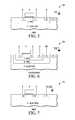
- FIGS. 5 , 6 , and 7show partial cross sectional views of a PMOS transistor 501 , an isolated NMOS transistor 601 , and an NMOS transistor 701 , respectively.
- Srepresents the source region contact
- Grepresents the gate contact
- Drepresents the drain region contact
- Brepresents the body contact for biasing the body.
- the substrateis of a P-type doping that is biased at VSS.
- Transistor 601includes an isolating N-well tub or region (labeled “N-Well” in FIG.
- a source region and a drain regionare current electrodes for a MOSFET.
- a gateis a control electrode for a MOSFET.
- FIG. 8shows another embodiment of transmission gate circuitry 111 .
- the circuitry of the embodiment of FIG. 8is similar to the circuitry of the embodiment of FIG. 2 , except for the circuitry controlling the gate voltages of NMOS transistor 208 and PMOS transistor 209 .
- the gate of NMOS transistor 208is connected to the gate of transistor 219 (node “EN”) to receive the enable signal, and the transistor body of transistor 208 is biased at VSS.
- transistor 208is not an isolated NMOS transistor. Instead it is similar to transistor 701 of FIG. 7 .
- transistor 208can be an isolated NMOS transistor where the isolating N-well region is biased to VDD or VBIAS 2 .
- the gate of PMOS transistor 209is connected to the drain of transistor 219 , and the transistor body of transistor 209 is biased at VBIAS 2 .
- FIG. 8do not include self enable circuitry 214 . Instead, an externally provided enable signal is used to make transistor 219 and transistor 208 conductive when VMPPAD is less than VDD.
- control circuitry and transmission gatesare implemented with MOSFETS.
- other embodimentsmay be implemented with other types of transistors including the transmission gates implemented with other types of switching devices.
- other embodimentsmay include a different number of transmission gates.
- the embodiments shown and described hereinprovide for a transmission gate circuit where the voltage drop across the transmission gate circuit, when in a non conductive mode, can be outside of the safe operating voltage areas of the transistors of the transmission gate wherein the voltage drop across any one transistor of the transmission gate circuit does not exceed its safe operating voltage.
- the transmission gate circuitcan be constructed of transistors with smaller safe operating voltage areas.
- transistors having smaller safe operating voltage areastypically are faster, easier to make, and/or occupy less area than transistors with higher safe operating voltage areas.
- a transmission gate circuitincludes a first transmission gate comprising a first switching device having a first current electrode, a second current electrode, and a control electrode.
- the transmission gate circuitincludes a second transmission gate comprising a second switching device having a first current electrode, a second current electrode, and a control electrode.
- the first current electrode of the second switching deviceis coupled to the second current electrode of the first switching device.
- the transmission gate circuitincludes a first terminal coupled to the first current electrode of the first switching device, a second terminal coupled to the second current electrode of the second switching device, and control circuitry coupled to the first transmission gate and the second transmission gate.
- the control circuitryplaces the first transmission gate and the second transmission gate into a conductive state to provide a conductive path between the first terminal and the second terminal through the first transmission gate and the second transmission gate, and when the control circuitry is in a second mode, the control circuitry places the first transmission gate and the second transmission gate into a non-conductive state.
- the control circuitryis in the second mode and a voltage of the first terminal is outside a safe operating voltage area of at least one of the first switching device and the second switching device, the first switching device remains within its safe operating voltage area and the second switching device remains within its safe operating voltage area.
- a methodin an embodiment of an integrated circuit comprising a first terminal, transmission gate circuitry coupled to the first terminal, and first circuitry coupled to the transmission gate circuitry, includes when a voltage of the first terminal is at or below a first voltage, placing the transmission gate circuitry into a conductive state to provide a conductive path between the first terminal and the first circuitry through the transmission gate circuitry. When the voltage of the first terminal is above the first voltage, the method further includes placing the transmission gate circuitry into a non-conductive state wherein the first circuitry is isolated from the first terminal and when the voltage of the first terminal is outside a safe operating voltage of at least one transistor within the transmission gate circuitry, maintaining each transistor within the transmission gate circuitry within its safe operating voltage area.
- a transmission gate circuitin another embodiment, includes a first transmission gate having a first terminal and a second terminal, and comprising a first NMOS transistor and a first PMOS transistor.
- the first NMOS transistoris coupled in parallel with the first PMOS transistor.
- a control electrode of the first NMOS transistoris coupled to a terminal of a first bias voltage.
- the transmission gate circuitincludes a second transmission gate having a third terminal and a fourth terminal and comprising a second NMOS transistor and a second PMOS transistor.
- the second NMOS transistoris coupled in parallel with the second PMOS transistor.
- the third terminalis coupled to the second terminal.
- the transmission gate circuitincludes a third PMOS transistor having a first current electrode coupled to the first terminal, a second current electrode coupled to a control electrode of the first PMOS transistor, and having a control electrode coupled to the terminal of the first bias voltage.
- the transmission gate circuitincludes a third NMOS transistor having a first current electrode coupled to the second current electrode of the third PMOS transistor, a second current electrode, and a control electrode coupled to the terminal of the first bias voltage.
- the transmission gate circuitincludes a fourth NMOS transistor having a first current electrode coupled to the second current electrode of the third NMOS transistor, a second current electrode, and a control electrode coupled to receive an enable signal.
- each of the first transmission gate and the second transmission gateWhen the enable signal is asserted, each of the first transmission gate and the second transmission gate is placed in a conductive state to provide a conductive path between the first terminal and the fourth terminal through the first transmission gate and the second transmission gate and when the enable signal is deasserted, each of the first transmission gate and the second transmission gate are placed in a non-conductive state.
Landscapes
- Semiconductor Integrated Circuits (AREA)
- Logic Circuits (AREA)
- Metal-Oxide And Bipolar Metal-Oxide Semiconductor Integrated Circuits (AREA)
- Semiconductor Memories (AREA)
- Non-Volatile Memory (AREA)
- Electronic Switches (AREA)
Abstract
Description
Claims (22)
Priority Applications (5)
| Application Number | Priority Date | Filing Date | Title |
|---|---|---|---|
| US12/824,991US8228109B2 (en) | 2010-06-28 | 2010-06-28 | Transmission gate circuitry for high voltage terminal |
| CN201180032138.4ACN102959863B (en) | 2010-06-28 | 2011-05-09 | Transmission gates for high voltage terminals |
| EP20110807201EP2586127A4 (en) | 2010-06-28 | 2011-05-09 | Transmission gate circuitry for high voltage terminal |
| JP2013518394AJP5767323B2 (en) | 2010-06-28 | 2011-05-09 | Transmission gate circuit for high voltage terminals and method of operation thereof |
| PCT/US2011/035727WO2012009042A1 (en) | 2010-06-28 | 2011-05-09 | Transmission gate circuitry for high voltage terminal |
Applications Claiming Priority (1)
| Application Number | Priority Date | Filing Date | Title |
|---|---|---|---|
| US12/824,991US8228109B2 (en) | 2010-06-28 | 2010-06-28 | Transmission gate circuitry for high voltage terminal |
Publications (2)
| Publication Number | Publication Date |
|---|---|
| US20110316610A1 US20110316610A1 (en) | 2011-12-29 |
| US8228109B2true US8228109B2 (en) | 2012-07-24 |
Family
ID=45351965
Family Applications (1)
| Application Number | Title | Priority Date | Filing Date |
|---|---|---|---|
| US12/824,991Active2030-10-09US8228109B2 (en) | 2010-06-28 | 2010-06-28 | Transmission gate circuitry for high voltage terminal |
Country Status (5)
| Country | Link |
|---|---|
| US (1) | US8228109B2 (en) |
| EP (1) | EP2586127A4 (en) |
| JP (1) | JP5767323B2 (en) |
| CN (1) | CN102959863B (en) |
| WO (1) | WO2012009042A1 (en) |
Cited By (8)
| Publication number | Priority date | Publication date | Assignee | Title |
|---|---|---|---|---|
| US20140240036A1 (en)* | 2013-02-28 | 2014-08-28 | Renesas Electronics Corporation | Semiconductor device |
| US9941883B2 (en) | 2015-04-03 | 2018-04-10 | Nxp Usa, Inc. | Transmission gate circuit |
| US10236873B2 (en)* | 2015-03-17 | 2019-03-19 | Xilinx, Inc. | Analog switch having reduced gate-induced drain leakage |
| US10972096B2 (en) | 2019-06-28 | 2021-04-06 | Nxp Usa, Inc. | Electronic switch |
| US11190178B1 (en)* | 2020-10-28 | 2021-11-30 | Xilinx, Inc. | Gate induced drain leakage robust bootstrapped switch |
| US11454668B2 (en) | 2019-12-30 | 2022-09-27 | Taiwan Semiconductor Manufacturing Company, Ltd. | Voltage tracking circuit and method of operating the same |
| US11639958B2 (en) | 2019-12-30 | 2023-05-02 | Taiwan Semiconductor Manufacturing Company, Ltd. | Voltage tracking circuit and method of operating the same |
| TWI824867B (en)* | 2022-12-05 | 2023-12-01 | 財團法人工業技術研究院 | Switching circuit and programmable connection chip |
Families Citing this family (4)
| Publication number | Priority date | Publication date | Assignee | Title |
|---|---|---|---|---|
| US9401711B2 (en)* | 2014-11-14 | 2016-07-26 | International Business Machines Corporation | Driver output with dynamic switching bias |
| CN105827224B (en)* | 2016-03-16 | 2018-09-25 | 中国科学院上海微系统与信息技术研究所 | A kind of high pressure simulation integrated switching circuit |
| CN109450436B (en)* | 2018-12-29 | 2024-02-09 | 上海艾为电子技术股份有限公司 | Drive circuit and level conversion circuit of signal transmission tube |
| FR3143915A1 (en)* | 2022-12-16 | 2024-06-21 | Stmicroelectronics International N.V. | INTEGRATED CIRCUIT INCLUDING A DIGITAL-ANALOG CONVERTER |
Citations (11)
| Publication number | Priority date | Publication date | Assignee | Title |
|---|---|---|---|---|
| US4930037A (en) | 1989-02-16 | 1990-05-29 | Advaced Micro Devices, Inc. | Input voltage protection system |
| US6097238A (en)* | 1997-01-10 | 2000-08-01 | Xilinx, Inc. | Circuit with ramp-up control and overcoming a threshold voltage loss in an NMOS transistor |
| US6127855A (en) | 1998-08-14 | 2000-10-03 | National Semiconductor Corporation | Switch-capacitor circuit with overdrive-protected switch |
| US6462611B2 (en)* | 1997-04-24 | 2002-10-08 | Kabushiki Kaisha Toshiba | Transmission gate |
| US20030218231A1 (en) | 2002-05-24 | 2003-11-27 | Sani Mehdi Hamidi | Non-volatile multi-threshold CMOS latch with leakage control |
| US6795369B2 (en) | 2002-11-22 | 2004-09-21 | Samsung Electronics Co., Ltd. | Address buffer and semiconductor memory device using the same |
| US6834336B2 (en) | 1997-06-16 | 2004-12-21 | Matsushita Electric Industrial Co., Ltd. | Processor for executing highly efficient VLIW |
| US20050189963A1 (en) | 2003-05-28 | 2005-09-01 | Fujitsu Limited | Semiconductor device |
| US6975271B2 (en)* | 2003-02-26 | 2005-12-13 | Matsushita Electric Industrial Co., Ltd. | Antenna switch module, all-in-one communication module, communication apparatus and method for manufacturing antenna switch module |
| US7286001B2 (en)* | 2003-06-12 | 2007-10-23 | Matsushita Electric Industrial Co., Ltd. | High-frequency switching device and semiconductor device |
| US7514983B2 (en) | 2007-03-23 | 2009-04-07 | Fairchild Semiconductor Corporation | Over-voltage tolerant pass-gate |
Family Cites Families (11)
| Publication number | Priority date | Publication date | Assignee | Title |
|---|---|---|---|---|
| US5691947A (en)* | 1992-12-18 | 1997-11-25 | Motorola Inc. | Multiplexed programming voltage and status over single conductor |
| KR100202195B1 (en)* | 1996-09-03 | 1999-06-15 | 문정환 | Over-power cut-off circuit |
| US6163199A (en)* | 1999-01-29 | 2000-12-19 | Fairchild Semiconductor Corp. | Overvoltage/undervoltage tolerant transfer gate |
| JP3722741B2 (en)* | 2001-11-15 | 2005-11-30 | 松下電器産業株式会社 | Voltage supply circuit |
| US6603331B1 (en)* | 2001-12-18 | 2003-08-05 | Xilinx, Inc. | Low-voltage non-degenerative transmitter circuit |
| US6700431B1 (en)* | 2002-09-10 | 2004-03-02 | Exar Corporation | I/O pad overvoltage protection circuitry |
| KR100495667B1 (en)* | 2003-01-13 | 2005-06-16 | 삼성전자주식회사 | Input output buffer providing analog/digital input mode |
| US7012794B2 (en)* | 2003-01-17 | 2006-03-14 | Exar Corporation | CMOS analog switch with auto over-voltage turn-off |
| US7400171B1 (en)* | 2005-05-03 | 2008-07-15 | Lattice Semiconductor Corporation | Electronic switch having extended voltage range |
| US7236002B2 (en)* | 2005-09-15 | 2007-06-26 | Dialog Semiconductor Gmbh | Digital CMOS-input with N-channel extended drain transistor for high-voltage protection |
| JP4939335B2 (en)* | 2007-08-07 | 2012-05-23 | ルネサスエレクトロニクス株式会社 | Bidirectional switch circuit |
- 2010
- 2010-06-28USUS12/824,991patent/US8228109B2/enactiveActive
- 2011
- 2011-05-09WOPCT/US2011/035727patent/WO2012009042A1/enactiveApplication Filing
- 2011-05-09CNCN201180032138.4Apatent/CN102959863B/ennot_activeExpired - Fee Related
- 2011-05-09JPJP2013518394Apatent/JP5767323B2/ennot_activeExpired - Fee Related
- 2011-05-09EPEP20110807201patent/EP2586127A4/ennot_activeWithdrawn
Patent Citations (12)
| Publication number | Priority date | Publication date | Assignee | Title |
|---|---|---|---|---|
| US4930037A (en) | 1989-02-16 | 1990-05-29 | Advaced Micro Devices, Inc. | Input voltage protection system |
| US6097238A (en)* | 1997-01-10 | 2000-08-01 | Xilinx, Inc. | Circuit with ramp-up control and overcoming a threshold voltage loss in an NMOS transistor |
| US6307420B1 (en)* | 1997-01-10 | 2001-10-23 | Xilinx, Inc. | Circuit with ramp-up control for overcoming a threshold voltage loss in an NMOS transistor |
| US6462611B2 (en)* | 1997-04-24 | 2002-10-08 | Kabushiki Kaisha Toshiba | Transmission gate |
| US6834336B2 (en) | 1997-06-16 | 2004-12-21 | Matsushita Electric Industrial Co., Ltd. | Processor for executing highly efficient VLIW |
| US6127855A (en) | 1998-08-14 | 2000-10-03 | National Semiconductor Corporation | Switch-capacitor circuit with overdrive-protected switch |
| US20030218231A1 (en) | 2002-05-24 | 2003-11-27 | Sani Mehdi Hamidi | Non-volatile multi-threshold CMOS latch with leakage control |
| US6795369B2 (en) | 2002-11-22 | 2004-09-21 | Samsung Electronics Co., Ltd. | Address buffer and semiconductor memory device using the same |
| US6975271B2 (en)* | 2003-02-26 | 2005-12-13 | Matsushita Electric Industrial Co., Ltd. | Antenna switch module, all-in-one communication module, communication apparatus and method for manufacturing antenna switch module |
| US20050189963A1 (en) | 2003-05-28 | 2005-09-01 | Fujitsu Limited | Semiconductor device |
| US7286001B2 (en)* | 2003-06-12 | 2007-10-23 | Matsushita Electric Industrial Co., Ltd. | High-frequency switching device and semiconductor device |
| US7514983B2 (en) | 2007-03-23 | 2009-04-07 | Fairchild Semiconductor Corporation | Over-voltage tolerant pass-gate |
Non-Patent Citations (1)
| Title |
|---|
| PCT/US2011/035727 International Search Report and Written Opinion mailed Dec. 26, 2011. |
Cited By (13)
| Publication number | Priority date | Publication date | Assignee | Title |
|---|---|---|---|---|
| US8901985B2 (en)* | 2013-02-28 | 2014-12-02 | Renesas Electronics Corporation | Semiconductor device |
| US9325168B2 (en) | 2013-02-28 | 2016-04-26 | Renesas Electronics Corporation | Semiconductor device |
| US20140240036A1 (en)* | 2013-02-28 | 2014-08-28 | Renesas Electronics Corporation | Semiconductor device |
| US10236873B2 (en)* | 2015-03-17 | 2019-03-19 | Xilinx, Inc. | Analog switch having reduced gate-induced drain leakage |
| US9941883B2 (en) | 2015-04-03 | 2018-04-10 | Nxp Usa, Inc. | Transmission gate circuit |
| US10972096B2 (en) | 2019-06-28 | 2021-04-06 | Nxp Usa, Inc. | Electronic switch |
| US11959960B2 (en) | 2019-12-30 | 2024-04-16 | Taiwan Semiconductor Manufacturing Company, Ltd. | Voltage tracking circuit and method of operating the same |
| US11454668B2 (en) | 2019-12-30 | 2022-09-27 | Taiwan Semiconductor Manufacturing Company, Ltd. | Voltage tracking circuit and method of operating the same |
| US11639958B2 (en) | 2019-12-30 | 2023-05-02 | Taiwan Semiconductor Manufacturing Company, Ltd. | Voltage tracking circuit and method of operating the same |
| US12259429B2 (en) | 2019-12-30 | 2025-03-25 | Taiwan Semiconductor Manufacturing Company, Ltd. | Voltage tracking circuit and method of operating the same |
| US11190178B1 (en)* | 2020-10-28 | 2021-11-30 | Xilinx, Inc. | Gate induced drain leakage robust bootstrapped switch |
| US12231086B2 (en) | 2022-12-05 | 2025-02-18 | Industrial Technology Research Institute | Switch circuit and programmable connection chip |
| TWI824867B (en)* | 2022-12-05 | 2023-12-01 | 財團法人工業技術研究院 | Switching circuit and programmable connection chip |
Also Published As
| Publication number | Publication date |
|---|---|
| CN102959863B (en) | 2015-09-23 |
| JP2013539249A (en) | 2013-10-17 |
| EP2586127A1 (en) | 2013-05-01 |
| JP5767323B2 (en) | 2015-08-19 |
| US20110316610A1 (en) | 2011-12-29 |
| WO2012009042A1 (en) | 2012-01-19 |
| CN102959863A (en) | 2013-03-06 |
| EP2586127A4 (en) | 2014-02-12 |
Similar Documents
| Publication | Publication Date | Title |
|---|---|---|
| US8228109B2 (en) | Transmission gate circuitry for high voltage terminal | |
| US10305474B2 (en) | High voltage output driver with low voltage devices | |
| US7369446B2 (en) | Method and apparatus to prevent high voltage supply degradation for high-voltage latches of a non-volatile memory | |
| US7605636B2 (en) | Power gating structure, semiconductor including the same and method of controlling a power gating | |
| US10348301B2 (en) | Output driving circuit | |
| US7834677B2 (en) | Transmission gate with body effect compensation circuit | |
| US11387830B2 (en) | Output driving circuit | |
| CN107408946B (en) | Transistor configured for gate over-biasing and circuit therefrom | |
| US9264045B2 (en) | Buffer circuit with reduced static leakage through controlled body biasing in FDSOI technology | |
| CN112786570B (en) | Integrated circuit with electrostatic discharge protection mechanism | |
| US9941883B2 (en) | Transmission gate circuit | |
| US8947122B2 (en) | Non-volatile latch structures with small area for FPGA | |
| US8049555B2 (en) | Low leakage sampling switch | |
| US8817432B2 (en) | Power switch embedded in ESD PAD | |
| US9620185B1 (en) | Voltage supply devices generating voltages applied to nonvolatile memory cells | |
| US8085604B2 (en) | Snap-back tolerant integrated circuits | |
| US9178508B2 (en) | High voltage switch with two or more outputs | |
| US9571101B2 (en) | Semiconductor device | |
| US8633731B1 (en) | Programmable integrated circuit with thin-oxide passgates | |
| US8228115B1 (en) | Circuit for biasing a well from three voltages | |
| US20250038525A1 (en) | Electro-static discharge (esd) protection circuit and electronic device including esd protection circuit | |
| CN106301349B (en) | High-voltage level conversion circuit | |
| US20240386952A1 (en) | Non-volatile memory device | |
| US20250098332A1 (en) | Power clamp circuit and electronic device including power clamp circuit | |
| TWI448076B (en) | High voltage sustainable output buffer |
Legal Events
| Date | Code | Title | Description |
|---|---|---|---|
| AS | Assignment | Owner name:FREESCALE SEMICONDUCTOR, INC., TEXAS Free format text:ASSIGNMENT OF ASSIGNORS INTEREST;ASSIGNORS:STOCKINGER, MICHAEL A.;CAMARENA, JOSE A.;ZHANG, WENZHONG;SIGNING DATES FROM 20100625 TO 20100628;REEL/FRAME:024632/0115 | |
| AS | Assignment | Owner name:CITIBANK, N.A., AS COLLATERAL AGENT, NEW YORK Free format text:SECURITY AGREEMENT;ASSIGNOR:FREESCALE SEMICONDUCTOR, INC.;REEL/FRAME:027622/0075 Effective date:20120116 Owner name:CITIBANK, N.A., AS COLLATERAL AGENT, NEW YORK Free format text:SECURITY AGREEMENT;ASSIGNOR:FREESCALE SEMICONDUCTOR, INC.;REEL/FRAME:027621/0928 Effective date:20120116 Owner name:CITIBANK, N.A., AS COLLATERAL AGENT, NEW YORK Free format text:SECURITY AGREEMENT;ASSIGNOR:FREESCALE SEMICONDUCTOR, INC.;REEL/FRAME:027622/0477 Effective date:20120116 | |
| STCF | Information on status: patent grant | Free format text:PATENTED CASE | |
| AS | Assignment | Owner name:CITIBANK, N.A., AS NOTES COLLATERAL AGENT, NEW YORK Free format text:SECURITY AGREEMENT;ASSIGNOR:FREESCALE SEMICONDUCTOR, INC.;REEL/FRAME:030633/0424 Effective date:20130521 Owner name:CITIBANK, N.A., AS NOTES COLLATERAL AGENT, NEW YOR Free format text:SECURITY AGREEMENT;ASSIGNOR:FREESCALE SEMICONDUCTOR, INC.;REEL/FRAME:030633/0424 Effective date:20130521 | |
| AS | Assignment | Owner name:CITIBANK, N.A., AS NOTES COLLATERAL AGENT, NEW YORK Free format text:SECURITY AGREEMENT;ASSIGNOR:FREESCALE SEMICONDUCTOR, INC.;REEL/FRAME:031591/0266 Effective date:20131101 Owner name:CITIBANK, N.A., AS NOTES COLLATERAL AGENT, NEW YOR Free format text:SECURITY AGREEMENT;ASSIGNOR:FREESCALE SEMICONDUCTOR, INC.;REEL/FRAME:031591/0266 Effective date:20131101 | |
| AS | Assignment | Owner name:FREESCALE SEMICONDUCTOR, INC., TEXAS Free format text:PATENT RELEASE;ASSIGNOR:CITIBANK, N.A., AS COLLATERAL AGENT;REEL/FRAME:037357/0334 Effective date:20151207 Owner name:FREESCALE SEMICONDUCTOR, INC., TEXAS Free format text:PATENT RELEASE;ASSIGNOR:CITIBANK, N.A., AS COLLATERAL AGENT;REEL/FRAME:037357/0285 Effective date:20151207 Owner name:FREESCALE SEMICONDUCTOR, INC., TEXAS Free format text:PATENT RELEASE;ASSIGNOR:CITIBANK, N.A., AS COLLATERAL AGENT;REEL/FRAME:037357/0387 Effective date:20151207 | |
| AS | Assignment | Owner name:MORGAN STANLEY SENIOR FUNDING, INC., MARYLAND Free format text:ASSIGNMENT AND ASSUMPTION OF SECURITY INTEREST IN PATENTS;ASSIGNOR:CITIBANK, N.A.;REEL/FRAME:037486/0517 Effective date:20151207 | |
| AS | Assignment | Owner name:MORGAN STANLEY SENIOR FUNDING, INC., MARYLAND Free format text:ASSIGNMENT AND ASSUMPTION OF SECURITY INTEREST IN PATENTS;ASSIGNOR:CITIBANK, N.A.;REEL/FRAME:037518/0292 Effective date:20151207 | |
| FPAY | Fee payment | Year of fee payment:4 | |
| AS | Assignment | Owner name:MORGAN STANLEY SENIOR FUNDING, INC., MARYLAND Free format text:SUPPLEMENT TO THE SECURITY AGREEMENT;ASSIGNOR:FREESCALE SEMICONDUCTOR, INC.;REEL/FRAME:039138/0001 Effective date:20160525 | |
| AS | Assignment | Owner name:NXP, B.V., F/K/A FREESCALE SEMICONDUCTOR, INC., NETHERLANDS Free format text:RELEASE BY SECURED PARTY;ASSIGNOR:MORGAN STANLEY SENIOR FUNDING, INC.;REEL/FRAME:040925/0001 Effective date:20160912 Owner name:NXP, B.V., F/K/A FREESCALE SEMICONDUCTOR, INC., NE Free format text:RELEASE BY SECURED PARTY;ASSIGNOR:MORGAN STANLEY SENIOR FUNDING, INC.;REEL/FRAME:040925/0001 Effective date:20160912 | |
| AS | Assignment | Owner name:NXP B.V., NETHERLANDS Free format text:RELEASE BY SECURED PARTY;ASSIGNOR:MORGAN STANLEY SENIOR FUNDING, INC.;REEL/FRAME:040928/0001 Effective date:20160622 | |
| AS | Assignment | Owner name:NXP USA, INC., TEXAS Free format text:MERGER;ASSIGNOR:FREESCALE SEMICONDUCTOR, INC.;REEL/FRAME:041144/0363 Effective date:20161107 | |
| AS | Assignment | Owner name:MORGAN STANLEY SENIOR FUNDING, INC., MARYLAND Free format text:CORRECTIVE ASSIGNMENT TO CORRECT THE REMOVE PATENTS 8108266 AND 8062324 AND REPLACE THEM WITH 6108266 AND 8060324 PREVIOUSLY RECORDED ON REEL 037518 FRAME 0292. ASSIGNOR(S) HEREBY CONFIRMS THE ASSIGNMENT AND ASSUMPTION OF SECURITY INTEREST IN PATENTS;ASSIGNOR:CITIBANK, N.A.;REEL/FRAME:041703/0536 Effective date:20151207 | |
| AS | Assignment | Owner name:SHENZHEN XINGUODU TECHNOLOGY CO., LTD., CHINA Free format text:CORRECTIVE ASSIGNMENT TO CORRECT THE TO CORRECT THE APPLICATION NO. FROM 13,883,290 TO 13,833,290 PREVIOUSLY RECORDED ON REEL 041703 FRAME 0536. ASSIGNOR(S) HEREBY CONFIRMS THE THE ASSIGNMENT AND ASSUMPTION OF SECURITYINTEREST IN PATENTS.;ASSIGNOR:MORGAN STANLEY SENIOR FUNDING, INC.;REEL/FRAME:048734/0001 Effective date:20190217 | |
| AS | Assignment | Owner name:NXP B.V., NETHERLANDS Free format text:RELEASE BY SECURED PARTY;ASSIGNOR:MORGAN STANLEY SENIOR FUNDING, INC.;REEL/FRAME:050744/0097 Effective date:20190903 | |
| AS | Assignment | Owner name:MORGAN STANLEY SENIOR FUNDING, INC., MARYLAND Free format text:CORRECTIVE ASSIGNMENT TO CORRECT THE REMOVE APPLICATION11759915 AND REPLACE IT WITH APPLICATION 11759935 PREVIOUSLY RECORDED ON REEL 037486 FRAME 0517. ASSIGNOR(S) HEREBY CONFIRMS THE ASSIGNMENT AND ASSUMPTION OF SECURITYINTEREST IN PATENTS;ASSIGNOR:CITIBANK, N.A.;REEL/FRAME:053547/0421 Effective date:20151207 | |
| MAFP | Maintenance fee payment | Free format text:PAYMENT OF MAINTENANCE FEE, 8TH YEAR, LARGE ENTITY (ORIGINAL EVENT CODE: M1552); ENTITY STATUS OF PATENT OWNER: LARGE ENTITY Year of fee payment:8 | |
| AS | Assignment | Owner name:NXP B.V., NETHERLANDS Free format text:CORRECTIVE ASSIGNMENT TO CORRECT THE REMOVEAPPLICATION 11759915 AND REPLACE IT WITH APPLICATION11759935 PREVIOUSLY RECORDED ON REEL 040928 FRAME 0001. ASSIGNOR(S) HEREBY CONFIRMS THE RELEASE OF SECURITYINTEREST;ASSIGNOR:MORGAN STANLEY SENIOR FUNDING, INC.;REEL/FRAME:052915/0001 Effective date:20160622 | |
| AS | Assignment | Owner name:NXP, B.V. F/K/A FREESCALE SEMICONDUCTOR, INC., NETHERLANDS Free format text:CORRECTIVE ASSIGNMENT TO CORRECT THE REMOVEAPPLICATION 11759915 AND REPLACE IT WITH APPLICATION11759935 PREVIOUSLY RECORDED ON REEL 040925 FRAME 0001. ASSIGNOR(S) HEREBY CONFIRMS THE RELEASE OF SECURITYINTEREST;ASSIGNOR:MORGAN STANLEY SENIOR FUNDING, INC.;REEL/FRAME:052917/0001 Effective date:20160912 | |
| MAFP | Maintenance fee payment | Free format text:PAYMENT OF MAINTENANCE FEE, 12TH YEAR, LARGE ENTITY (ORIGINAL EVENT CODE: M1553); ENTITY STATUS OF PATENT OWNER: LARGE ENTITY Year of fee payment:12 |