US8228023B2 - Charging systems and methods for thin-film lithium-ion battery - Google Patents
Charging systems and methods for thin-film lithium-ion batteryDownload PDFInfo
- Publication number
- US8228023B2 US8228023B2US12/069,440US6944008AUS8228023B2US 8228023 B2US8228023 B2US 8228023B2US 6944008 AUS6944008 AUS 6944008AUS 8228023 B2US8228023 B2US 8228023B2
- Authority
- US
- United States
- Prior art keywords
- battery
- charging
- circuit
- voltage
- electrical contact
- Prior art date
- Legal status (The legal status is an assumption and is not a legal conclusion. Google has not performed a legal analysis and makes no representation as to the accuracy of the status listed.)
- Expired - Fee Related, expires
Links
- 229910001416lithium ionInorganic materials0.000titleclaimsdescription32
- HBBGRARXTFLTSG-UHFFFAOYSA-NLithium ionChemical compound[Li+]HBBGRARXTFLTSG-UHFFFAOYSA-N0.000titleclaimsdescription31
- 239000010409thin filmSubstances0.000titleclaimsdescription18
- 238000000034methodMethods0.000titleabstractdescription31
- 238000004146energy storageMethods0.000abstractdescription18
- 238000006243chemical reactionMethods0.000abstractdescription8
- 238000002955isolationMethods0.000abstractdescription4
- 238000007599dischargingMethods0.000abstractdescription3
- 239000000758substrateSubstances0.000description24
- XUIMIQQOPSSXEZ-UHFFFAOYSA-NSiliconChemical compound[Si]XUIMIQQOPSSXEZ-UHFFFAOYSA-N0.000description11
- 229910052710siliconInorganic materials0.000description11
- 239000010703siliconSubstances0.000description11
- 229910052744lithiumInorganic materials0.000description9
- WHXSMMKQMYFTQS-UHFFFAOYSA-NLithiumChemical compound[Li]WHXSMMKQMYFTQS-UHFFFAOYSA-N0.000description8
- RYGMFSIKBFXOCR-UHFFFAOYSA-NCopperChemical compound[Cu]RYGMFSIKBFXOCR-UHFFFAOYSA-N0.000description7
- 229910052802copperInorganic materials0.000description7
- 239000010949copperSubstances0.000description7
- 238000010586diagramMethods0.000description7
- 239000000463materialSubstances0.000description7
- 239000004033plasticSubstances0.000description6
- 238000000151depositionMethods0.000description5
- 239000003792electrolyteSubstances0.000description5
- 230000006870functionEffects0.000description5
- 229910052751metalInorganic materials0.000description5
- 230000008901benefitEffects0.000description4
- 229920000642polymerPolymers0.000description4
- 229910052782aluminiumInorganic materials0.000description3
- XAGFODPZIPBFFR-UHFFFAOYSA-NaluminiumChemical compound[Al]XAGFODPZIPBFFR-UHFFFAOYSA-N0.000description3
- 230000004888barrier functionEffects0.000description3
- 239000003990capacitorSubstances0.000description3
- 230000003750conditioning effectEffects0.000description3
- 238000013461designMethods0.000description3
- 238000003306harvestingMethods0.000description3
- 238000004519manufacturing processMethods0.000description3
- 239000002184metalSubstances0.000description3
- 239000004065semiconductorSubstances0.000description3
- IJGRMHOSHXDMSA-UHFFFAOYSA-NAtomic nitrogenChemical compoundN#NIJGRMHOSHXDMSA-UHFFFAOYSA-N0.000description2
- VYZAMTAEIAYCRO-UHFFFAOYSA-NChromiumChemical compound[Cr]VYZAMTAEIAYCRO-UHFFFAOYSA-N0.000description2
- 229910001290LiPF6Inorganic materials0.000description2
- 239000010405anode materialSubstances0.000description2
- 230000033228biological regulationEffects0.000description2
- 239000010406cathode materialSubstances0.000description2
- 239000000919ceramicSubstances0.000description2
- 229910052804chromiumInorganic materials0.000description2
- 239000011651chromiumSubstances0.000description2
- 238000004891communicationMethods0.000description2
- 230000003247decreasing effectEffects0.000description2
- 230000008021depositionEffects0.000description2
- 230000009977dual effectEffects0.000description2
- 230000005611electricityEffects0.000description2
- 230000001939inductive effectEffects0.000description2
- 230000010354integrationEffects0.000description2
- 150000002500ionsChemical class0.000description2
- 238000002161passivationMethods0.000description2
- RUOJZAUFBMNUDX-UHFFFAOYSA-Npropylene carbonateChemical compoundCC1COC(=O)O1RUOJZAUFBMNUDX-UHFFFAOYSA-N0.000description2
- 230000001681protective effectEffects0.000description2
- 239000007787solidSubstances0.000description2
- 238000004544sputter depositionMethods0.000description2
- TWQULNDIKKJZPH-UHFFFAOYSA-Ktrilithium;phosphateChemical group[Li+].[Li+].[Li+].[O-]P([O-])([O-])=OTWQULNDIKKJZPH-UHFFFAOYSA-K0.000description2
- 229910000838Al alloyInorganic materials0.000description1
- OKTJSMMVPCPJKN-UHFFFAOYSA-NCarbonChemical compound[C]OKTJSMMVPCPJKN-UHFFFAOYSA-N0.000description1
- 229910001030Iron–nickel alloyInorganic materials0.000description1
- 239000002200LIPON - lithium phosphorus oxynitrideSubstances0.000description1
- VYPSYNLAJGMNEJ-UHFFFAOYSA-NSilicium dioxideChemical compoundO=[Si]=OVYPSYNLAJGMNEJ-UHFFFAOYSA-N0.000description1
- 101100397044Xenopus laevis invs-a geneProteins0.000description1
- 101100397045Xenopus laevis invs-b geneProteins0.000description1
- 230000009471actionEffects0.000description1
- 230000004913activationEffects0.000description1
- 229910045601alloyInorganic materials0.000description1
- 239000000956alloySubstances0.000description1
- 238000004458analytical methodMethods0.000description1
- QVGXLLKOCUKJST-UHFFFAOYSA-Natomic oxygenChemical compound[O]QVGXLLKOCUKJST-UHFFFAOYSA-N0.000description1
- 239000011230binding agentSubstances0.000description1
- 230000005540biological transmissionEffects0.000description1
- 230000000903blocking effectEffects0.000description1
- 239000011248coating agentSubstances0.000description1
- 238000000576coating methodMethods0.000description1
- 239000004020conductorSubstances0.000description1
- 230000009849deactivationEffects0.000description1
- 230000003412degenerative effectEffects0.000description1
- 230000000779depleting effectEffects0.000description1
- 230000001627detrimental effectEffects0.000description1
- 238000010292electrical insulationMethods0.000description1
- 239000008151electrolyte solutionSubstances0.000description1
- 238000009713electroplatingMethods0.000description1
- 238000004049embossingMethods0.000description1
- 238000005516engineering processMethods0.000description1
- 239000010408filmSubstances0.000description1
- 238000001914filtrationMethods0.000description1
- 238000009472formulationMethods0.000description1
- 239000000446fuelSubstances0.000description1
- 239000011521glassSubstances0.000description1
- BHEPBYXIRTUNPN-UHFFFAOYSA-Nhydridophosphorus(.) (triplet)Chemical compound[PH]BHEPBYXIRTUNPN-UHFFFAOYSA-N0.000description1
- 230000006872improvementEffects0.000description1
- 230000006698inductionEffects0.000description1
- 239000011810insulating materialSubstances0.000description1
- 239000012212insulatorSubstances0.000description1
- 230000000670limiting effectEffects0.000description1
- 230000007246mechanismEffects0.000description1
- 238000001465metallisationMethods0.000description1
- VNWKTOKETHGBQD-UHFFFAOYSA-NmethaneChemical compoundCVNWKTOKETHGBQD-UHFFFAOYSA-N0.000description1
- 238000004377microelectronicMethods0.000description1
- 239000000203mixtureSubstances0.000description1
- 238000012986modificationMethods0.000description1
- 230000004048modificationEffects0.000description1
- 238000012544monitoring processMethods0.000description1
- 229910052757nitrogenInorganic materials0.000description1
- 239000005486organic electrolyteSubstances0.000description1
- 229910052760oxygenInorganic materials0.000description1
- 239000001301oxygenSubstances0.000description1
- 238000007639printingMethods0.000description1
- 230000008569processEffects0.000description1
- 238000011112process operationMethods0.000description1
- 238000012545processingMethods0.000description1
- 239000000376reactantSubstances0.000description1
- 230000002829reductive effectEffects0.000description1
- 230000002441reversible effectEffects0.000description1
- 229910052594sapphireInorganic materials0.000description1
- 239000010980sapphireSubstances0.000description1
- 229920006395saturated elastomerPolymers0.000description1
- 229910052814silicon oxideInorganic materials0.000description1
- 229910000679solderInorganic materials0.000description1
- 239000010935stainless steelSubstances0.000description1
- 229910001220stainless steelInorganic materials0.000description1
- 238000006467substitution reactionMethods0.000description1
- 231100000331toxicToxicity0.000description1
- 230000002588toxic effectEffects0.000description1
- XLYOFNOQVPJJNP-UHFFFAOYSA-NwaterChemical compoundOXLYOFNOQVPJJNP-UHFFFAOYSA-N0.000description1
Images


Classifications
- H—ELECTRICITY
- H01—ELECTRIC ELEMENTS
- H01M—PROCESSES OR MEANS, e.g. BATTERIES, FOR THE DIRECT CONVERSION OF CHEMICAL ENERGY INTO ELECTRICAL ENERGY
- H01M10/00—Secondary cells; Manufacture thereof
- H01M10/05—Accumulators with non-aqueous electrolyte
- H01M10/052—Li-accumulators
- H01M10/0525—Rocking-chair batteries, i.e. batteries with lithium insertion or intercalation in both electrodes; Lithium-ion batteries
- H—ELECTRICITY
- H01—ELECTRIC ELEMENTS
- H01M—PROCESSES OR MEANS, e.g. BATTERIES, FOR THE DIRECT CONVERSION OF CHEMICAL ENERGY INTO ELECTRICAL ENERGY
- H01M10/00—Secondary cells; Manufacture thereof
- H01M10/04—Construction or manufacture in general
- H01M10/0436—Small-sized flat cells or batteries for portable equipment
- H—ELECTRICITY
- H01—ELECTRIC ELEMENTS
- H01M—PROCESSES OR MEANS, e.g. BATTERIES, FOR THE DIRECT CONVERSION OF CHEMICAL ENERGY INTO ELECTRICAL ENERGY
- H01M10/00—Secondary cells; Manufacture thereof
- H01M10/05—Accumulators with non-aqueous electrolyte
- H01M10/052—Li-accumulators
- H—ELECTRICITY
- H01—ELECTRIC ELEMENTS
- H01M—PROCESSES OR MEANS, e.g. BATTERIES, FOR THE DIRECT CONVERSION OF CHEMICAL ENERGY INTO ELECTRICAL ENERGY
- H01M10/00—Secondary cells; Manufacture thereof
- H01M10/05—Accumulators with non-aqueous electrolyte
- H01M10/056—Accumulators with non-aqueous electrolyte characterised by the materials used as electrolytes, e.g. mixed inorganic/organic electrolytes
- H01M10/0561—Accumulators with non-aqueous electrolyte characterised by the materials used as electrolytes, e.g. mixed inorganic/organic electrolytes the electrolyte being constituted of inorganic materials only
- H01M10/0562—Solid materials
- H—ELECTRICITY
- H01—ELECTRIC ELEMENTS
- H01M—PROCESSES OR MEANS, e.g. BATTERIES, FOR THE DIRECT CONVERSION OF CHEMICAL ENERGY INTO ELECTRICAL ENERGY
- H01M10/00—Secondary cells; Manufacture thereof
- H01M10/05—Accumulators with non-aqueous electrolyte
- H01M10/058—Construction or manufacture
- H01M10/0585—Construction or manufacture of accumulators having only flat construction elements, i.e. flat positive electrodes, flat negative electrodes and flat separators
- H—ELECTRICITY
- H01—ELECTRIC ELEMENTS
- H01M—PROCESSES OR MEANS, e.g. BATTERIES, FOR THE DIRECT CONVERSION OF CHEMICAL ENERGY INTO ELECTRICAL ENERGY
- H01M10/00—Secondary cells; Manufacture thereof
- H01M10/42—Methods or arrangements for servicing or maintenance of secondary cells or secondary half-cells
- H01M10/46—Accumulators structurally combined with charging apparatus
- H—ELECTRICITY
- H01—ELECTRIC ELEMENTS
- H01M—PROCESSES OR MEANS, e.g. BATTERIES, FOR THE DIRECT CONVERSION OF CHEMICAL ENERGY INTO ELECTRICAL ENERGY
- H01M14/00—Electrochemical current or voltage generators not provided for in groups H01M6/00 - H01M12/00; Manufacture thereof
- H—ELECTRICITY
- H01—ELECTRIC ELEMENTS
- H01M—PROCESSES OR MEANS, e.g. BATTERIES, FOR THE DIRECT CONVERSION OF CHEMICAL ENERGY INTO ELECTRICAL ENERGY
- H01M50/00—Constructional details or processes of manufacture of the non-active parts of electrochemical cells other than fuel cells, e.g. hybrid cells
- H01M50/10—Primary casings; Jackets or wrappings
- H01M50/102—Primary casings; Jackets or wrappings characterised by their shape or physical structure
- H01M50/11—Primary casings; Jackets or wrappings characterised by their shape or physical structure having a chip structure, e.g. micro-sized batteries integrated on chips
- H—ELECTRICITY
- H01—ELECTRIC ELEMENTS
- H01M—PROCESSES OR MEANS, e.g. BATTERIES, FOR THE DIRECT CONVERSION OF CHEMICAL ENERGY INTO ELECTRICAL ENERGY
- H01M6/00—Primary cells; Manufacture thereof
- H01M6/40—Printed batteries, e.g. thin film batteries
- H—ELECTRICITY
- H02—GENERATION; CONVERSION OR DISTRIBUTION OF ELECTRIC POWER
- H02J—CIRCUIT ARRANGEMENTS OR SYSTEMS FOR SUPPLYING OR DISTRIBUTING ELECTRIC POWER; SYSTEMS FOR STORING ELECTRIC ENERGY
- H02J7/00—Circuit arrangements for charging or depolarising batteries or for supplying loads from batteries
- H02J7/0068—Battery or charger load switching, e.g. concurrent charging and load supply
- H—ELECTRICITY
- H01—ELECTRIC ELEMENTS
- H01M—PROCESSES OR MEANS, e.g. BATTERIES, FOR THE DIRECT CONVERSION OF CHEMICAL ENERGY INTO ELECTRICAL ENERGY
- H01M10/00—Secondary cells; Manufacture thereof
- H01M10/42—Methods or arrangements for servicing or maintenance of secondary cells or secondary half-cells
- H01M10/44—Methods for charging or discharging
- Y—GENERAL TAGGING OF NEW TECHNOLOGICAL DEVELOPMENTS; GENERAL TAGGING OF CROSS-SECTIONAL TECHNOLOGIES SPANNING OVER SEVERAL SECTIONS OF THE IPC; TECHNICAL SUBJECTS COVERED BY FORMER USPC CROSS-REFERENCE ART COLLECTIONS [XRACs] AND DIGESTS
- Y02—TECHNOLOGIES OR APPLICATIONS FOR MITIGATION OR ADAPTATION AGAINST CLIMATE CHANGE
- Y02E—REDUCTION OF GREENHOUSE GAS [GHG] EMISSIONS, RELATED TO ENERGY GENERATION, TRANSMISSION OR DISTRIBUTION
- Y02E60/00—Enabling technologies; Technologies with a potential or indirect contribution to GHG emissions mitigation
- Y02E60/10—Energy storage using batteries
- Y—GENERAL TAGGING OF NEW TECHNOLOGICAL DEVELOPMENTS; GENERAL TAGGING OF CROSS-SECTIONAL TECHNOLOGIES SPANNING OVER SEVERAL SECTIONS OF THE IPC; TECHNICAL SUBJECTS COVERED BY FORMER USPC CROSS-REFERENCE ART COLLECTIONS [XRACs] AND DIGESTS
- Y10—TECHNICAL SUBJECTS COVERED BY FORMER USPC
- Y10T—TECHNICAL SUBJECTS COVERED BY FORMER US CLASSIFICATION
- Y10T29/00—Metal working
- Y10T29/49—Method of mechanical manufacture
- Y10T29/49002—Electrical device making
- Y10T29/49108—Electric battery cell making
- Y10T29/49115—Electric battery cell making including coating or impregnating
Definitions
- the inventiongenerally relates to systems and methods for electrical signal conditioning.
- the systems and methods for electrical conditioningare applied to solid-state thin-film battery charging.
- Portable devicestypically use batteries as power supplies. Batteries must have sufficient capacity to power the device for at least the length of time the device is in use. Sufficient battery capacity can result in a power supply that is quite heavy and/or large compared to the rest of the device. Accordingly, smaller and lighter batteries (i.e., power supplies) with sufficient energy storage are desired.
- Other energy storage devicessuch as supercapacitors, and energy conversion devices, such as photovoltaics and fuel cells, are alternatives to batteries for use as power supplies in portable electronics and non-portable electrical applications.
- One type of an energy-storage deviceis a solid-state, thin-film battery.
- Examples of thin-film batteriesare described in U.S. Pat. Nos. 5,314,765; 5,338,625; 5,445,906; 5,512,147; 5,561,004; 5,567,210; 5,569,520; 5,597,660; 5,612,152; 5,654,084; and 5,705,293, each of which is herein incorporated by reference.
- U.S. Pat. No. 5,338,625describes a thin-film battery, especially a thin-film microbattery, and a method for making same having application as a backup or first integrated power source for electronic devices.
- U.S. Pat. No. 5,445,906describes a method and system for manufacturing a thin-film battery structure formed with the method that utilizes a plurality of deposition stations at which thin battery component films are built up in sequence upon a web-like substrate as the substrate is automatically moved through the stations.
- a conductive substratee.g., a metal such as copper or aluminum
- a thin film of LiPON(Lithium Phosphorous OxyNitride) is then formed by low-pressure ( ⁇ 10 mtorr) sputter deposition of lithium orthophosphate (Li3PO4) in nitrogen.
- LiPONLithium Phosphorous OxyNitride
- Li3PO4lithium orthophosphate
- LiPONwas deposited over the copper anode contact to a thickness of 2.5 microns, and a layer of lithium metal was formed onto the copper anode contact by electroplating though the LiPON layer in a propylene carbonate/LiPF6 electrolyte solution.
- the air cathodewas a carbon-powder/polyfluoroacrylate-binder coating (Novec-1700) saturated with a propylene carbonate/LiPF6 organic electrolyte solution.
- a cathode-contact layer having carbon granulesis deposited, such that atmospheric oxygen could operate as the cathode reactant. This configuration requires providing air access to substantially the entire cathode surface, limiting the ability to densely stack layers for higher electrical capacity (i.e., amphours).
- electrical capacityi.e., amphours
- a method and apparatus for a unitary battery and charging circuitthat includes a first substrate having integrated-circuit battery-charging circuitry thereon, and a cathode material, an anode material, and an electrolyte layer separating the cathode material from the anode material deposited on the substrate to form a battery, wherein the charging circuit is connected to the battery and encapsulated to form a surface-mount unitary package.
- a power conversion system and methodthat includes a variable charging source and an energy storage device.
- the power conversion circuitalso includes a charging circuit coupled to the variable charging source and the energy storage device, the energy storage device being charged by the variable charging source.
- the circuitincludes an energy storage device isolation circuit configured to isolate the energy storage device from discharging when power from the variable charging source is below a predetermined threshold.
- the conversion circuitincludes a restart circuit configured to restart the charging circuit by utilizing power from the energy storage device when charging power has dropped below a predetermined level.
- the charging systemcomprises a variable charging source.
- the charging systemalso comprises an energy storage device.
- the charging systemcomprises a charging circuit coupled to the variable charging source and the energy storage device.
- the energy storage deviceis charged by the variable charging source.
- the charging circuitincludes a charge pump and a microcontroller controlling the charge pump.
- the charge pumpboosts the charge to a predetermined threshold and the microcontroller controlling the output of the charge pump such that the output of the charge pump maintains a relatively steady output voltage at least for a period of time where sufficient charge power is available from the variable charging source.
- FIG. 1is an exemplary schematic cross-section view of a partially manufactured layered structure 100 for a unitary package having a solid-state cell (e.g., Lithium-ion battery cell) built onto the silicon substrate and its charging circuitry built into the silicon substrate of some embodiments of the invention, also showing contact areas of the cell that are photolithographically defined and the cells (optionally photo-lithographic techniques are also used to singulate the cell with the exception of substrate support tabs).
- a solid-state celle.g., Lithium-ion battery cell
- FIG. 2is an exemplary schematic of the unitary package having a solid-state cell (e.g., Lithiumion battery cell) and its charging circuitry (a 3-terminal device with input, output and ground terminals.
- a solid-state celle.g., Lithiumion battery cell
- its charging circuitrya 3-terminal device with input, output and ground terminals.
- FIG. 3is an exemplary schematic of the unitary package having a solid-state cell (e.g., Lithiumion battery cell) and its charging circuitry (a 4-terminal device with input, control signal to start and/or stop the charging, output and ground terminals).
- a solid-state celle.g., Lithiumion battery cell
- its charging circuitrya 4-terminal device with input, control signal to start and/or stop the charging, output and ground terminals.
- FIG. 4is an exemplary schematic cross-section view of a partially manufactured layered structure 400 for a unitary package having a solid-state cell (e.g., Lithium-ion battery cell) built onto the silicon substrate and its charging circuitry, which is separately fabricated and later attached onto the silicon substrate of some embodiments of the invention.
- a solid-state celle.g., Lithium-ion battery cell
- FIG. 5is an exemplary schematic perspective view of the unitary package having a solid-state cell (e.g., Lithium-ion battery cell) and its charging circuitry encapsulated in the plastic of an SMT package (a 3-terminal device with input, output and ground terminals.
- a solid-state celle.g., Lithium-ion battery cell
- SMT packagea 3-terminal device with input, output and ground terminals.
- FIG. 6is a schematic of the unitary package having a solid-state cell (e.g., Lithium-ion battery cell) and its inductive charging circuitry.
- a solid-state celle.g., Lithium-ion battery cell
- FIG. 7is a schematic of the unitary package having a solid-state cell (e.g., Lithium-ion battery cell) and its charging circuitry (a 2-terminal device with input/output and ground terminals), according to some embodiments of the invention.
- a solid-state celle.g., Lithium-ion battery cell
- its charging circuitrya 2-terminal device with input/output and ground terminals
- FIG. 8is a schematic of the unitary package having a solid-state cell (e.g., Lithium-ion battery cell) and its charging circuitry (a 3-terminal device with input, output and ground terminals), according to some embodiments of the invention.
- a solid-state celle.g., Lithium-ion battery cell
- its charging circuitrya 3-terminal device with input, output and ground terminals
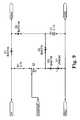
- FIG. 9is a schematic of the unitary package having a solid-state cell (e.g., Lithium-ion battery cell) and its charging circuitry (a 4-terminal device with input, control signal to start and/or stop the charging, output and ground terminals), according to some embodiments of the invention.
- a solid-state celle.g., Lithium-ion battery cell
- its charging circuitrya 4-terminal device with input, control signal to start and/or stop the charging, output and ground terminals
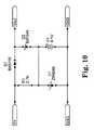
- FIG. 10is a schematic of the unitary package having a solid-state cell (e.g., Lithium-ion battery cell) and its charging circuitry (a 3-terminal device with input, output and ground terminals), according to some embodiments of the invention.
- a solid-state celle.g., Lithium-ion battery cell
- its charging circuitrya 3-terminal device with input, output and ground terminals
- FIG. 11is a schematic of the unitary package having a solid-state cell (e.g., Lithium-ion battery cell) and its charging circuitry (a 3-terminal device with input, output and ground terminals), according to some embodiments of the invention.
- a solid-state celle.g., Lithium-ion battery cell
- its charging circuitrya 3-terminal device with input, output and ground terminals
- FIG. 12is a schematic of the unitary package having a solid-state cell (e.g., Lithium-ion battery cell) and its charging circuitry (a 3-terminal device with input, output and ground terminals), according to some embodiments of the invention.
- a solid-state celle.g., Lithium-ion battery cell
- its charging circuitrya 3-terminal device with input, output and ground terminals
- FIG. 13is a schematic of the unitary package having a solid-state cell (e.g., Lithium-ion battery cell) and its charging circuitry (a 4-terminal device with input, control signal to start and/or stop the charging, output and ground terminals), according to some embodiments of the invention.
- a solid-state celle.g., Lithium-ion battery cell
- its charging circuitrya 4-terminal device with input, control signal to start and/or stop the charging, output and ground terminals
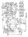
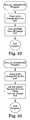
- FIG. 14is a schematic of an energy harvesting and charging circuit, according to some embodiments of the invention.
- FIG. 15is an alternative schematic of an energy harvesting and charging circuit, according to some embodiments of the invention.
- FIG. 16is a block diagram and schematic of an exemplary charging system using a charge pump and microcontroller, according to some embodiments of the invention.
- FIG. 17is a schematic of a microcontroller charge pump, according to some embodiments of the invention.
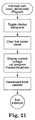
- FIGS. 18-29are flow diagrams for the software for the microcontroller charge pump, according to some embodiments of the invention.
- the inventionincludes, but is not limited to a novel structural combination of conventional data/signal processing components and communications circuits, and not in the particular detailed configurations thereof. Accordingly, the structure, methods, functions, control and arrangement of conventional components and circuits have, for the most part, been illustrated in the drawings by readily understandable block representations and schematic diagrams, in order not to obscure the disclosure with structural details which will be readily apparent to those skilled in the art, having the benefit of the description herein. Further, the invention is not limited to the particular embodiments depicted in the exemplary diagrams, but should be construed in accordance with the language in the claims.
- metalapplies both to substantially pure single metallic elements and to alloys or combinations of two or more elements, at least one of which is a metallic element.
- substratesgenerally refers to the physical structure that is the basic work piece that is transformed by various process operations into the desired microelectronic configuration.
- substratesinclude conducting material (such as copper, stainless steel, aluminum and the like), insulating material (such as sapphire, ceramic, or plastic/polymer insulators and the like), semiconducting materials (such as silicon), nonsemiconducting, or combinations of semiconducting and non-semiconducting materials.
- substratesinclude layered structures, such as a core sheet or piece of material (such as iron-nickel alloy and the like) chosen for its coefficient of thermal expansion (CTE) that more closely matches the CTE of an adjacent structure such as a silicon processor chip.
- CTEcoefficient of thermal expansion
- such a substrate coreis laminated to a sheet of material chosen for electrical and/or thermal conductivity (such as a copper, aluminum alloy and the like), which in turn is covered with a layer of plastic chosen for electrical insulation, stability, and embossing characteristics.
- An electrolyteis a material that conducts electricity by allowing movement of ions (e.g., lithium ions having a positive charge) while being non-conductive to electrons.
- An electrical cell or batteryis a device having an anode and a cathode that are separated by an electrolyte.
- a dielectricis a material that is non-conducting to electricity, such as, for example, plastic, ceramic, or glass.
- a material such as LiPONcan act as an electrolyte when a source and sink for lithium are adjacent the LiPON layer, and can also act as a dielectric when placed between two metal layers such as copper or aluminum, which do not form ions that can pass through the LiPON.
- devicesinclude an insulating plastic/polymer layer (a dielectric) having wiring traces that carry signals and electrical power horizontally, and vias that carry signals and electrical power vertically between layers of traces.
- verticalis defined to mean substantially perpendicular to the major surface of a substrate. Height or depth refers to a distance in a direction perpendicular to the major surface of a substrate.
- FIG. 1is a schematic cross-section view of a partially manufactured layered structure 100 for a unitary package having a solid-state cell (e.g., Lithium-ion battery cell) built onto the silicon substrate and its charging circuitry built into the silicon substrate of some embodiments of the invention, also showing contact areas of the cell that are photo-lithographically defined and the cells (optionally photo-lithographic techniques are also used to singulate the cell with the exception of substrate support tabs).
- structure 100includes stacked or multiple battery cells, with associated charging circuitry, providing a higher output voltage.
- FIG. 2is a schematic of the unitary package 200 having a solid-state cell (e.g., Lithiumion battery cell) and its charging circuitry (a 3-terminal device with input, output and ground terminals), according to some embodiments of the invention.
- a solid-state celle.g., Lithiumion battery cell
- its charging circuitrya 3-terminal device with input, output and ground terminals
- FIG. 3is a schematic of the unitary package 300 having a solid-state cell (e.g., Lithiumion battery cell) and its charging circuitry (a 4-terminal device with input, control signal to start and/or stop the charging, output and ground terminals), according to some embodiments of the invention.
- a solid-state celle.g., Lithiumion battery cell
- its charging circuitrya 4-terminal device with input, control signal to start and/or stop the charging, output and ground terminals
- FIG. 4is a schematic cross-section view of a partially manufactured layered structure 400 for a unitary package having a solid-state cell (e.g., Lithium-ion battery cell) built onto the silicon substrate and its charging circuitry, which is separately fabricated and later attached onto the silicon substrate of some embodiments of the invention.
- a solid-state celle.g., Lithium-ion battery cell
- FIG. 5is a schematic perspective view of the unitary package having a solid-state cell (e.g., Lithium-ion battery cell) and its charging circuitry encapsulated in the plastic of an SMT package (a 3-terminal device with input, output and ground terminals), according to some embodiments of the invention.
- the battery and charging circuitryare encapsulated into a unitary package, such as a epoxy-encapsulated surface mount technology (SMT) package to be soldered to a printed circuit.
- SMTsurface mount technology
- FIG. 6is a schematic of the unitary package having a solid-state cell (e.g., Lithium-ion battery cell) and its inductive charging circuitry, according to some embodiments of the invention.
- a solid-state celle.g., Lithium-ion battery cell
- inductive charging circuitrye.g., Lithium-ion battery cell
- Various methodsmay be employed to charge a thin-film battery that has the properties of being solid state and thus is more robust that conventional lithium-ion and lithium polymer cells with respect to recharge methods.
- such methodsinclude solar cells, magnetic induction, thermoelectric devices, and piezoelectric materials.
- What makes the circuit in FIG. 6 viable for the thin-film solid state batteryis the fact that the battery may be charged efficiently using a potentiostatic charging regimen, without need for constant current sources, safety circuits, charge counters, or timers.
- the charging deviceis amenable to direct integration with the battery, but is not essential that it be so integrated.
- the batteryis recharged by means of receiving energy through a secondary coil coupled magnetically to a primary coil, via electrical contacts and intervened by a voltage regulator to clamp the voltage at a level consistent with the charging voltage of the battery.
- the filtering circuitryi.e., capacitor C 1
- Other embodimentsmay employ and include Boost, Buck Boost, or other switching energy management topologies.
- FIG. 7a schematic of the unitary package having a solid-state cell (e.g., Lithium-ion battery cell) and its charging circuitry (a 2-terminal device with input/output and ground terminals), according to some embodiments of the invention is depicted.
- a solid-state celle.g., Lithium-ion battery cell
- its charging circuitrya 2-terminal device with input/output and ground terminals
- a control lineis driven by a timer that charges the battery for a fixed period of time, then disconnects the charging voltage from the battery. This can be used in cases where extended charging times are detrimental to the battery and/or in cases where it is desirable to shut off the zener current to conserve power.
- the diagramshows a timer, but the control line could also be driven by any number of integrated circuits that have outputs that can be driven high or low according to elapsed time or other events occurring.
- Diode D 4could also be a BAS116 in order to use a quad diode pack.
- U 2could be any number of devices, including a timer, microcontrollers, signal processor, supply supervisor, etc., having an output to control the activation/deactivation of the charge control circuit. Integration of these charge control components can be accomplished in a variety of ways:
- the discrete componentscan be packaged in a multi-chip module using wirebonding or solder bumps to establish connections to the package exterior.
- One of the metallization layers deposited during battery manufacturecan serve as the interconnect between the charge control components and the battery itself, thus minimizing discrete component count, overall package footprint, and assembly cost.
- FIG. 8a schematic of the unitary package having a solid-state cell (e.g., Lithium-ion battery cell) and its charging circuitry (a 3-terminal device with input, output and ground terminals), according to some embodiments of the invention is depicted.
- diode D 4could be replaced with the same diode used for D 1 , D 2 , and D 3 , so that a quad diode pack (or two dual packs) could be used.
- BAV170is a suitable substitute for BAS116.
- Many other diode typesare also available and can be used depending on the forward voltage drop and reverse current blocking characteristics, in addition to size and cost considerations.
- FIG. 9is a schematic of the unitary package having a solid-state cell (e.g., Lithium-ion battery cell) and its charging circuitry (a 4-terminal device with input, control signal to start and/or stop the charging, output and ground terminals), according to some embodiments of the invention.
- Q 2is optional and is suited for very low power applications, where the charge control circuit can be switched on and off according to certain events or to simply conserve power.
- the /Charge linecan be driven high or low from a timer, for example.
- a quad diode packcould provide D 1 , D 2 , D 3 , and D 4 .
- FIG. 10a schematic of the unitary package having a solid-state cell (e.g., Lithium-ion battery cell) and its charging circuitry (a 3-terminal device with input, output and ground terminals), according to some embodiments of the invention is depicted.
- Diode D 1may be replaced with the same diode used for D 2 so that a dual diode pack could be used.
- BAV170is a suitable substitute for BAS116.
- All of the components in the diagramscan be purchased in small, inexpensive, leaded or leadless surface mount formats, thus allowing these circuits to be embedded in a single package such as a leadless chip carrier (LCC), multi-chip module (MCM), ball grid array (BGA), micro-BGA (uBGA), system in package (SiP), and other package types, either with or without the inclusion of the thin film battery for which the control circuit is designed to charge.
- LCCleadless chip carrier
- MCMmulti-chip module
- BGAball grid array
- uBGAmicro-BGA
- SiPsystem in package
- other package typeseither with or without the inclusion of the thin film battery for which the control circuit is designed to charge.
- FIG. 11is a schematic of the unitary package having a solid-state cell (e.g., Lithium-ion battery cell) and its charging circuitry (a 3-terminal device with input, output and ground terminals), according to some embodiments of the invention.
- the circuituses analog transmission gates for isolation.
- inv 1 and inv 2are powered in the battery voltage domain.
- FIG. 12a schematic of the unitary package having a solid-state cell (e.g., Lithium-ion battery cell) and its charging circuitry (a 3-terminal device with input, output and ground terminals), according to some embodiments of the invention is depicted.
- a solid-state celle.g., Lithium-ion battery cell
- its charging circuitrya 3-terminal device with input, output and ground terminals
- FIG. 13depicts an exemplary schematic of the unitary package having a solid-state cell (e.g., Lithium-ion battery cell) and its charging circuitry (a 4-terminal device with input, control signal to start and/or stop the charging, output and ground terminals), according to some embodiments of the invention.
- a solid-state celle.g., Lithium-ion battery cell
- its charging circuitrya 4-terminal device with input, control signal to start and/or stop the charging, output and ground terminals
- Circuit 1400comprises a plurality of subsystems or sub-circuits.
- a subsystem 1410comprises an energy or power conversion circuit detailed in International Publication No. WO 2007/048052 having an international filing date of Oct. 23, 2006, entitled “SYSTEMS AND METHODS FOR RECEIVING AND MANAGING POWER IN WIRELESS DEVICES’, by Regan Zane et al. and which is herein incorporated by reference.
- Circuit 1410comprises a buck boost converter configuration including inductor L 1 which is energized as transistor Q 2 is turned on. The buck boost converter may function to maintain a relatively constant charging voltage.
- the voltage comparatorcomprising transistor Q 6 , and resistors R 8 , R 9 , and R 10 , drives switching to disconnect the batteries from the voltage regulator when there is insufficient voltage to charge the batteries. For example, transistors Q 3 A and Q 6 will turn off transistors Q 5 B and Q 3 B thereby isolating batteries BT 1 and BT 2 from the charging circuit.
- Integrated circuit U 1acts as a voltage regulator to monitor and control the charger voltage.
- Circuit 1410requires a threshold power to get initiated with a charger disable circuit 1420 .
- Q 1When the transducer voltage gets above a threshold value, Q 1 will turn on causing backflow through the path to pin 2 of the comparator U 3 .
- Charger disable circuit 1420provides an indication to the application circuit that there is sufficient power to charge the battery.
- Circuit 1820comprises two gate switches Q 5 B and Q 3 B which function to maintain isolation of the battery BT 1 and BT 2 selectively and maintaining zero leakage current when the batteries are not being charged or there is not sufficient power to do so. Circuit 1420 is further described in U.S. Publication No. 2008/0001577 A1, filed on Jul.
- Transistor Q 5 Ais used to send a signal to the microcontroller that no power is going to the battery for monitoring and control.
- Circuits 1410 and 1420combine to enable restarting of the charging circuits by utilizing power from the batteries at the point in which everything has been shut down.
- Circuit 1410comprises a low speed oscillator 1430 (e.g. operating at about 500 Hz) and a high speed oscillator 1440 .
- Low speed oscillatorgates the high speed oscillator (on/off) and helps to match the input impedance to the output impedance.
- the combination of circuits 1410 and 1420maintain several functions including but not limited to isolating battery from discharging to the charge circuits, starting the charging circuits after the charging circuits were shut down for lack of charging voltage, and isolating the batteries from the load when the battery voltage gets too low below a predetermined threshold.
- FIG. 15depicts a similar circuit to FIG. 14 but having improved performance characteristics.
- variable resistor R 19is used in the low speed oscillator circuit to precisely trim the oscillator frequency. This action provides improved efficiency in low light conditions. In very low light conditions, it may be possible that the circuit will attempt to operate but not have sufficient energy to charge the battery and thereby depleting the battery over time. Thus, the capacitor C 7 was removed from the circuit and the value of capacitor C 8 was decreased. Further, diode D 7 was added to the base of transistor Q 1 to raise the trip voltage of the transistor. These improvements provide assurance that sufficient energy is available in low light situations so that the battery will maintain more energy input than energy output.
- FET Q 4 A, resistor R 17 , and resistor R 18form a voltage comparator where the voltage present at the junction of R 18 and Q 4 B is divided by R 18 and R 17 and presented to the gate of Q 4 A.
- the divider ratio of R 17 and R 18is setup to be above the FET Q 4 A's VGS threshold voltage with, in accordance with an exemplary embodiment, a voltage of 3.6V or greater at the junction of R 18 and Q 4 B. If the voltage at the gate of Q 4 A is below the VGS threshold voltage (battery voltage is 3.6V or less) then Q 4 A will come out of its low resistance state and the drain voltage on Q 4 A will begin to rise.
- FET Q 4 A and Q 4 Bwill be turned on and the application circuit will also be turned on any time the energy transducer has sufficient voltage to trip voltage comparator Q 1 .
- FET Q 7 Athrough the addition of FET Q 7 A, FET Q 4 A and Q 4 B will be turned on and the application circuit will also be turned on only when the battery has been charged or more then enough energy is available to charge a depleted battery. This implementation insures that the application circuit will always have the benefit of a fully charged battery or sufficient energy when ever power is made available to the application circuit.
- resistors R 8 and R 9being larger to keep the output of the voltage regulator U 1 from going out of regulation (voltage to high) when the battery is fully charged without a load on the output in strong light conditions.
- the output cutoff circuitwas changed with the addition of Q 7 A so that the output will not be enabled until the battery is nearly fully charged.
- R 21 and C 3are connected to the gate of Q 7 A to keep the output from being pulsed on during low light conditions.
- the circuitmay be used to boost the voltage Vcc from a 3V level up to a level that is used to charge the battery (e.g. 4.1 V).
- a pulse width modulator (PWM) based A/Dmay be used as a charge pump, an example of which is depicted in FIG. 17 , to boost the incoming voltage in combination with a microcontroller (Battery Management Circuit).
- the microcontroller controlled charge pumpmay include software which helps to adjust signal frequency to the correct or sufficient level. Such software is detailed in the flow diagrams provided in FIGS. 18-29 .
- the microcontrollerinsures that the charge voltage is maintained at the desired input level.
- the circuitsare implemented in an ASIC, while in other embodiments, the circuits use one or more discreet components.
Landscapes
- Chemical & Material Sciences (AREA)
- Engineering & Computer Science (AREA)
- General Chemical & Material Sciences (AREA)
- Chemical Kinetics & Catalysis (AREA)
- Electrochemistry (AREA)
- Manufacturing & Machinery (AREA)
- Power Engineering (AREA)
- General Physics & Mathematics (AREA)
- Inorganic Chemistry (AREA)
- Condensed Matter Physics & Semiconductors (AREA)
- Physics & Mathematics (AREA)
- Materials Engineering (AREA)
- Charge And Discharge Circuits For Batteries Or The Like (AREA)
- Secondary Cells (AREA)
Abstract
Description
Claims (5)
Priority Applications (1)
| Application Number | Priority Date | Filing Date | Title |
|---|---|---|---|
| US12/069,440US8228023B2 (en) | 2007-02-09 | 2008-02-08 | Charging systems and methods for thin-film lithium-ion battery |
Applications Claiming Priority (2)
| Application Number | Priority Date | Filing Date | Title |
|---|---|---|---|
| US88926407P | 2007-02-09 | 2007-02-09 | |
| US12/069,440US8228023B2 (en) | 2007-02-09 | 2008-02-08 | Charging systems and methods for thin-film lithium-ion battery |
Publications (2)
| Publication Number | Publication Date |
|---|---|
| US20080203972A1 US20080203972A1 (en) | 2008-08-28 |
| US8228023B2true US8228023B2 (en) | 2012-07-24 |
Family
ID=39615821
Family Applications (1)
| Application Number | Title | Priority Date | Filing Date |
|---|---|---|---|
| US12/069,440Expired - Fee RelatedUS8228023B2 (en) | 2007-02-09 | 2008-02-08 | Charging systems and methods for thin-film lithium-ion battery |
Country Status (7)
| Country | Link |
|---|---|
| US (1) | US8228023B2 (en) |
| EP (1) | EP2111657A2 (en) |
| JP (2) | JP2010518578A (en) |
| KR (1) | KR20090113373A (en) |
| CN (1) | CN101657916A (en) |
| CA (1) | CA2677677A1 (en) |
| WO (1) | WO2008100441A2 (en) |
Cited By (14)
| Publication number | Priority date | Publication date | Assignee | Title |
|---|---|---|---|---|
| WO2013025919A1 (en) | 2011-08-17 | 2013-02-21 | Cymbet Corporation | Multi-cell thin film microbattery array |
| US20140015470A1 (en)* | 2012-07-11 | 2014-01-16 | Electronics And Telecommunications Research Institute | Wearable wireless power transmission apparatus and wireless power transmission method using the same |
| WO2014085578A1 (en) | 2012-11-29 | 2014-06-05 | Cymbet Corporation | Thin film microbattery charge and output control |
| DE102015109991A1 (en) | 2014-06-23 | 2015-12-24 | Schott Ag | Electrical storage system with disc-shaped discrete element, process for its manufacture and its use |
| DE102015109992A1 (en) | 2014-06-23 | 2015-12-24 | Schott Ag | Electrical storage system with disc-shaped discrete element, disk-shaped discrete element, process for its preparation and its use |
| DE102014117632A1 (en) | 2014-06-23 | 2015-12-24 | Schott Ag | An electrical storage system comprising a disk-shaped discrete element, disc-shaped discrete element, and methods of making and using the same |
| DE102015109994A1 (en) | 2014-06-23 | 2015-12-24 | Schott Ag | Electrical storage system with disc-shaped discrete element, disk-shaped discrete element, process for its preparation and its use |
| DE102014117640A1 (en) | 2014-12-01 | 2016-06-02 | Schott Ag | Electrical storage system with disc discrete element, discrete element, process for its manufacture and its use |
| US10116153B2 (en)* | 2016-08-24 | 2018-10-30 | Tianjin Synergy Groups Co., Ltd. | Mobile power supply capable of charging itself and electronic device |
| US10566584B2 (en) | 2014-06-23 | 2020-02-18 | Schott Ag | Electrical storage system with a sheet-like discrete element, sheet-like discrete element, method for producing same, and use thereof |
| US10673025B2 (en) | 2014-12-01 | 2020-06-02 | Schott Ag | Electrical storage system comprising a sheet-type discrete element, discrete sheet-type element, method for the production thereof, and use thereof |
| US10749218B2 (en)* | 2017-11-10 | 2020-08-18 | Qualcomm Incorporated | Circuitry for charging a multi-stack battery pack |
| US12300827B2 (en) | 2019-03-29 | 2025-05-13 | Murata Manufacturing Co., Ltd. | Solid-state battery |
| US12322820B2 (en) | 2020-04-02 | 2025-06-03 | Tdk Electronics Ag | Assembly for protecting an SMD component from environmental influences |
Families Citing this family (29)
| Publication number | Priority date | Publication date | Assignee | Title |
|---|---|---|---|---|
| CN101752626A (en)* | 2008-12-01 | 2010-06-23 | 深圳富泰宏精密工业有限公司 | Portable electronic device |
| FR2946461B1 (en)* | 2009-06-09 | 2011-07-22 | Commissariat Energie Atomique | DEVICE FOR FLEXIBLE ENCAPSULATION OF A MICRO-BATTERY |
| CA2779667A1 (en)* | 2009-11-02 | 2011-05-05 | Belkin International, Inc. | Battery backup system, method of use, and method of manufacturing |
| KR101831401B1 (en)* | 2010-01-26 | 2018-02-23 | 사임베트 코퍼레이션 | Battery arrays, construction and method |
| JP5638926B2 (en)* | 2010-11-30 | 2014-12-10 | ラピスセミコンダクタ株式会社 | Semiconductor chip |
| US8277246B2 (en)* | 2010-12-01 | 2012-10-02 | Nokia Corporation | Battery terminal adapter |
| DE102011086309A1 (en)* | 2011-11-14 | 2013-05-16 | Continental Automotive Gmbh | Circuit arrangement with counter-phase working charge pumps for charging an electrical energy storage |
| US9095077B2 (en) | 2011-11-30 | 2015-07-28 | Apple Inc. | Graphene heat dissipators in portable electronic devices |
| CN102570550A (en)* | 2012-01-12 | 2012-07-11 | 苏州清莲纳米环保科技有限公司 | Solar charger |
| EP2817845A4 (en)* | 2012-02-23 | 2015-10-21 | Cymbet Corp | Thin film battery charge control and method |
| CN103579707B (en)* | 2012-07-20 | 2016-01-06 | 纳米新能源(唐山)有限责任公司 | Self-charging lithium ion battery |
| SG2013067749A (en) | 2012-09-07 | 2014-04-28 | Agency Science Tech & Res | An energy harvesting apparatus and a method for operating an energy harvesting apparatus |
| US20140176041A1 (en)* | 2012-12-20 | 2014-06-26 | Nvidia Corporation | Semiconductor thermoelectric module charger for mobile computing device |
| US9444398B2 (en) | 2013-01-25 | 2016-09-13 | Taiwan Semiconductor Manufacturing Co., Ltd. | Semiconductor structure and fabricating process for the same |
| US9107335B2 (en)* | 2013-02-19 | 2015-08-11 | Infineon Technologies Ag | Method for manufacturing an integrated circuit and an integrated circuit |
| US9705151B2 (en)* | 2014-03-28 | 2017-07-11 | Infineon Technologies Ag | Battery, a battery element and a method for forming a battery |
| US9991550B2 (en)* | 2015-02-27 | 2018-06-05 | Verily Life Sciences Llc | Methods and devices associated with bonding of solid-state lithium batteries |
| WO2016176336A1 (en)* | 2015-04-27 | 2016-11-03 | Applied Materials, Inc. | Printed circuit board assembly with integrated circuit chip package and solid state battery |
| WO2017204859A1 (en)* | 2016-05-25 | 2017-11-30 | Applied Materials, Inc. | Configuration of solid state thin film batteries |
| JP6383051B2 (en)* | 2016-06-15 | 2018-08-29 | ラピスセミコンダクタ株式会社 | Semiconductor chip |
| TWI637668B (en)* | 2016-10-13 | 2018-10-01 | 輝能科技股份有限公司 | Logical battery |
| EP3602655A4 (en)* | 2017-03-20 | 2020-12-23 | Millibatt, Inc. | Battery system and production method |
| KR102063887B1 (en)* | 2017-07-05 | 2020-01-08 | 서상천 | High Speed Photovoltaic Module with Improved Charging Efficiency |
| TWI728381B (en)* | 2019-06-11 | 2021-05-21 | 賈叢林 | Adaptive Active Control Micro Battery Array |
| CN116438689A (en)* | 2020-08-19 | 2023-07-14 | 米莉巴特有限公司 | Three-dimensional folding battery pack and manufacturing method thereof |
| US11509754B1 (en)* | 2020-12-01 | 2022-11-22 | Gerald Kess, Jr. | Mobile communication and gaming device |
| CN113363592A (en)* | 2021-06-08 | 2021-09-07 | 四川启睿克科技有限公司 | Chip and battery integrated integration method and device |
| WO2023243489A1 (en)* | 2022-06-14 | 2023-12-21 | 株式会社村田製作所 | Solid battery package |
| CN115548478A (en)* | 2022-10-17 | 2022-12-30 | 上海天马微电子有限公司 | A battery array and battery device |
Citations (17)
| Publication number | Priority date | Publication date | Assignee | Title |
|---|---|---|---|---|
| US5314765A (en) | 1993-10-14 | 1994-05-24 | Martin Marietta Energy Systems, Inc. | Protective lithium ion conducting ceramic coating for lithium metal anodes and associate method |
| US5338625A (en) | 1992-07-29 | 1994-08-16 | Martin Marietta Energy Systems, Inc. | Thin film battery and method for making same |
| US5445906A (en) | 1994-08-03 | 1995-08-29 | Martin Marietta Energy Systems, Inc. | Method and system for constructing a rechargeable battery and battery structures formed with the method |
| US5561004A (en) | 1994-02-25 | 1996-10-01 | Bates; John B. | Packaging material for thin film lithium batteries |
| US5569520A (en) | 1994-01-12 | 1996-10-29 | Martin Marietta Energy Systems, Inc. | Rechargeable lithium battery for use in applications requiring a low to high power output |
| US5654084A (en) | 1994-07-22 | 1997-08-05 | Martin Marietta Energy Systems, Inc. | Protective coatings for sensitive materials |
| US5705293A (en) | 1997-01-09 | 1998-01-06 | Lockheed Martin Energy Research Corporation | Solid state thin film battery having a high temperature lithium alloy anode |
| WO2001073864A2 (en) | 2000-03-24 | 2001-10-04 | Cymbet Corporation | Thin-film battery having ultra-thin electrolyte and associated method |
| US20020171399A1 (en) | 1998-02-20 | 2002-11-21 | Fujitsu, Limited | Power supply apparatus with chargeable battery and charge/discharge method |
| US20040029311A1 (en) | 2002-08-09 | 2004-02-12 | Snyder Shawn W. | Methods of and device for encapsulation and termination of electronic devices |
| US20040258984A1 (en) | 2003-04-14 | 2004-12-23 | Massachusetts Institute Of Technology | Integrated thin film batteries on silicon integrated circuits |
| WO2005067645A2 (en) | 2004-01-06 | 2005-07-28 | Cymbet Corporation | Layered barrier structure having one or more definable layers and method |
| US20050237686A1 (en) | 2002-08-30 | 2005-10-27 | Yuji Satoh | Overdischarge preventing circuit apparatus and overdischarge preventing method |
| US20060132093A1 (en) | 2004-12-22 | 2006-06-22 | Nguyen Don J | Battery pack leakage cut-off |
| WO2007048052A2 (en) | 2005-10-21 | 2007-04-26 | The Regents Of The University Of Colorado | Systems and methods for receiving and managing power in wireless devices |
| US7211351B2 (en) | 2003-10-16 | 2007-05-01 | Cymbet Corporation | Lithium/air batteries with LiPON as separator and protective barrier and method |
| US20080001577A1 (en) | 2006-06-30 | 2008-01-03 | Cymbet Corporation | Thin-film battery recharging systems and methods |
Family Cites Families (9)
| Publication number | Priority date | Publication date | Assignee | Title |
|---|---|---|---|---|
| JPS6295936A (en)* | 1985-10-21 | 1987-05-02 | カシオ計算機株式会社 | Power supply circuit using solar cells |
| JP3610595B2 (en)* | 1994-07-20 | 2005-01-12 | 松下電器産業株式会社 | Cordless telephone equipment |
| JP3329168B2 (en)* | 1995-01-13 | 2002-09-30 | オムロン株式会社 | Backflow prevention device |
| JPH09259932A (en)* | 1996-03-26 | 1997-10-03 | Toshiba Battery Co Ltd | Secondary battery with charging circuit |
| JPH10208779A (en)* | 1997-01-27 | 1998-08-07 | Japan Storage Battery Co Ltd | Protective circuit for pack battery and secondary battery |
| JP2000102176A (en)* | 1998-09-21 | 2000-04-07 | Mitsubishi Cable Ind Ltd | Secondary battery pack |
| JP2000112577A (en)* | 1998-09-24 | 2000-04-21 | Internatl Business Mach Corp <Ibm> | Battery switching circuit |
| JP3531866B2 (en)* | 2000-07-28 | 2004-05-31 | 独立行政法人 科学技術振興機構 | Thin-film solid lithium ion secondary battery |
| US20040029321A1 (en)* | 2002-08-07 | 2004-02-12 | Chartered Semiconductor Manufacturing Ltd. | Method for forming gate insulating layer having multiple dielectric constants and multiple equivalent oxide thicknesses |
- 2008
- 2008-02-08WOPCT/US2008/001731patent/WO2008100441A2/enactiveApplication Filing
- 2008-02-08USUS12/069,440patent/US8228023B2/ennot_activeExpired - Fee Related
- 2008-02-08CACA002677677Apatent/CA2677677A1/ennot_activeAbandoned
- 2008-02-08JPJP2009549124Apatent/JP2010518578A/ennot_activeWithdrawn
- 2008-02-08KRKR1020097018686Apatent/KR20090113373A/ennot_activeCeased
- 2008-02-08EPEP08725373Apatent/EP2111657A2/ennot_activeWithdrawn
- 2008-02-08CNCN200880008800Apatent/CN101657916A/enactivePending
- 2013
- 2013-01-24JPJP2013011023Apatent/JP2013084624A/enactivePending
Patent Citations (26)
| Publication number | Priority date | Publication date | Assignee | Title |
|---|---|---|---|---|
| US5338625A (en) | 1992-07-29 | 1994-08-16 | Martin Marietta Energy Systems, Inc. | Thin film battery and method for making same |
| US5512147A (en) | 1992-07-29 | 1996-04-30 | Martin Marietta Energy Systems, Inc. | Method of making an electrolyte for an electrochemical cell |
| US5567210A (en) | 1992-07-29 | 1996-10-22 | Martin Marietta Energy Systems, Inc. | Method for making an electrochemical cell |
| US5597660A (en) | 1992-07-29 | 1997-01-28 | Martin Marietta Energy Systems, Inc. | Electrolyte for an electrochemical cell |
| US5314765A (en) | 1993-10-14 | 1994-05-24 | Martin Marietta Energy Systems, Inc. | Protective lithium ion conducting ceramic coating for lithium metal anodes and associate method |
| US5569520A (en) | 1994-01-12 | 1996-10-29 | Martin Marietta Energy Systems, Inc. | Rechargeable lithium battery for use in applications requiring a low to high power output |
| US5612152A (en) | 1994-01-12 | 1997-03-18 | Martin Marietta Energy Systems, Inc. | Rechargeable lithium battery for use in applications requiring a low to high power output |
| US5561004A (en) | 1994-02-25 | 1996-10-01 | Bates; John B. | Packaging material for thin film lithium batteries |
| US5654084A (en) | 1994-07-22 | 1997-08-05 | Martin Marietta Energy Systems, Inc. | Protective coatings for sensitive materials |
| US5445906A (en) | 1994-08-03 | 1995-08-29 | Martin Marietta Energy Systems, Inc. | Method and system for constructing a rechargeable battery and battery structures formed with the method |
| US5705293A (en) | 1997-01-09 | 1998-01-06 | Lockheed Martin Energy Research Corporation | Solid state thin film battery having a high temperature lithium alloy anode |
| US20020171399A1 (en) | 1998-02-20 | 2002-11-21 | Fujitsu, Limited | Power supply apparatus with chargeable battery and charge/discharge method |
| US20020037756A1 (en) | 2000-03-24 | 2002-03-28 | Integrated Power Solutions Inc. | Battery-operated wireless-communication apparatus and method |
| US7131189B2 (en)* | 2000-03-24 | 2006-11-07 | Cymbet Corporation | Continuous processing of thin-film batteries and like devices |
| US6805998B2 (en) | 2000-03-24 | 2004-10-19 | Cymbet Corporation | Method and apparatus for integrated-battery devices |
| WO2001073864A2 (en) | 2000-03-24 | 2001-10-04 | Cymbet Corporation | Thin-film battery having ultra-thin electrolyte and associated method |
| US7433655B2 (en)* | 2000-03-24 | 2008-10-07 | Cymbet Corporation | Battery-operated wireless-communication apparatus and method |
| US6924164B2 (en)* | 2000-03-24 | 2005-08-02 | Cymbet Corporation | Method of continuous processing of thin-film batteries and like devices |
| US20040029311A1 (en) | 2002-08-09 | 2004-02-12 | Snyder Shawn W. | Methods of and device for encapsulation and termination of electronic devices |
| US20050237686A1 (en) | 2002-08-30 | 2005-10-27 | Yuji Satoh | Overdischarge preventing circuit apparatus and overdischarge preventing method |
| US20040258984A1 (en) | 2003-04-14 | 2004-12-23 | Massachusetts Institute Of Technology | Integrated thin film batteries on silicon integrated circuits |
| US7211351B2 (en) | 2003-10-16 | 2007-05-01 | Cymbet Corporation | Lithium/air batteries with LiPON as separator and protective barrier and method |
| WO2005067645A2 (en) | 2004-01-06 | 2005-07-28 | Cymbet Corporation | Layered barrier structure having one or more definable layers and method |
| US20060132093A1 (en) | 2004-12-22 | 2006-06-22 | Nguyen Don J | Battery pack leakage cut-off |
| WO2007048052A2 (en) | 2005-10-21 | 2007-04-26 | The Regents Of The University Of Colorado | Systems and methods for receiving and managing power in wireless devices |
| US20080001577A1 (en) | 2006-06-30 | 2008-01-03 | Cymbet Corporation | Thin-film battery recharging systems and methods |
Non-Patent Citations (2)
| Title |
|---|
| International Search Report mailed Feb. 24, 2009 (7 pgs). |
| Sukumar, et al., "Switch array system for thin film lithium microbatteries," Journal of Power Sources, 136 (2004) 401-407. |
Cited By (17)
| Publication number | Priority date | Publication date | Assignee | Title |
|---|---|---|---|---|
| US9331501B2 (en) | 2011-08-17 | 2016-05-03 | Cymbet Corporation | Multi-cell thin film microbattery array |
| WO2013025919A1 (en) | 2011-08-17 | 2013-02-21 | Cymbet Corporation | Multi-cell thin film microbattery array |
| US20140015470A1 (en)* | 2012-07-11 | 2014-01-16 | Electronics And Telecommunications Research Institute | Wearable wireless power transmission apparatus and wireless power transmission method using the same |
| WO2014085578A1 (en) | 2012-11-29 | 2014-06-05 | Cymbet Corporation | Thin film microbattery charge and output control |
| US9419463B2 (en) | 2012-11-29 | 2016-08-16 | Cymbet Corporation | Thin film microbattery charge and output control |
| US10566584B2 (en) | 2014-06-23 | 2020-02-18 | Schott Ag | Electrical storage system with a sheet-like discrete element, sheet-like discrete element, method for producing same, and use thereof |
| DE102015109994A1 (en) | 2014-06-23 | 2015-12-24 | Schott Ag | Electrical storage system with disc-shaped discrete element, disk-shaped discrete element, process for its preparation and its use |
| DE102014117632A1 (en) | 2014-06-23 | 2015-12-24 | Schott Ag | An electrical storage system comprising a disk-shaped discrete element, disc-shaped discrete element, and methods of making and using the same |
| DE102015109992A1 (en) | 2014-06-23 | 2015-12-24 | Schott Ag | Electrical storage system with disc-shaped discrete element, disk-shaped discrete element, process for its preparation and its use |
| DE102015109991A1 (en) | 2014-06-23 | 2015-12-24 | Schott Ag | Electrical storage system with disc-shaped discrete element, process for its manufacture and its use |
| DE102014117640A1 (en) | 2014-12-01 | 2016-06-02 | Schott Ag | Electrical storage system with disc discrete element, discrete element, process for its manufacture and its use |
| US10418658B2 (en) | 2014-12-01 | 2019-09-17 | Schott Ag | Electrical storage system comprising a disc-shaped discrete element, discrete element, method for the production thereof, and use thereof |
| US10673025B2 (en) | 2014-12-01 | 2020-06-02 | Schott Ag | Electrical storage system comprising a sheet-type discrete element, discrete sheet-type element, method for the production thereof, and use thereof |
| US10116153B2 (en)* | 2016-08-24 | 2018-10-30 | Tianjin Synergy Groups Co., Ltd. | Mobile power supply capable of charging itself and electronic device |
| US10749218B2 (en)* | 2017-11-10 | 2020-08-18 | Qualcomm Incorporated | Circuitry for charging a multi-stack battery pack |
| US12300827B2 (en) | 2019-03-29 | 2025-05-13 | Murata Manufacturing Co., Ltd. | Solid-state battery |
| US12322820B2 (en) | 2020-04-02 | 2025-06-03 | Tdk Electronics Ag | Assembly for protecting an SMD component from environmental influences |
Also Published As
| Publication number | Publication date |
|---|---|
| US20080203972A1 (en) | 2008-08-28 |
| EP2111657A2 (en) | 2009-10-28 |
| JP2013084624A (en) | 2013-05-09 |
| KR20090113373A (en) | 2009-10-30 |
| CA2677677A1 (en) | 2008-08-21 |
| WO2008100441A3 (en) | 2009-04-16 |
| WO2008100441A2 (en) | 2008-08-21 |
| JP2010518578A (en) | 2010-05-27 |
| CN101657916A (en) | 2010-02-24 |
Similar Documents
| Publication | Publication Date | Title |
|---|---|---|
| US8228023B2 (en) | Charging systems and methods for thin-film lithium-ion battery | |
| US7624499B2 (en) | Flexible circuit having an integrally formed battery | |
| US20080001577A1 (en) | Thin-film battery recharging systems and methods | |
| JP3531866B2 (en) | Thin-film solid lithium ion secondary battery | |
| KR101606412B1 (en) | Battery layout incorporating full metal edge seal | |
| US20090278503A1 (en) | Thin-film battery equipment | |
| JP2025020432A (en) | Secondary Battery Module | |
| US9793573B2 (en) | Lithium ion secondary battery containing a non-polar active material | |
| CN112510296A (en) | Battery assembly, heating method thereof and electronic equipment | |
| Balog et al. | Batteries, battery management, and battery charging technology | |
| JP2003331800A (en) | Battery pack and battery charge / discharge circuit | |
| US8242590B2 (en) | Silicon wafer for semiconductor with powersupply system on the backside of wafer | |
| JP3176340B2 (en) | Method of manufacturing solar cell module | |
| US20250132585A1 (en) | Power module and electrical device | |
| JP2023525302A (en) | Battery device and its manufacturing method | |
| EP2745347B1 (en) | Multi-cell thin film microbattery array | |
| JPH0244660A (en) | Lithium battery with charging mechanism | |
| JP2004120950A (en) | Solar cell power supply | |
| JP3433751B2 (en) | Overcharge / overdischarge prevention device | |
| JPH0244778A (en) | Optical power source |
Legal Events
| Date | Code | Title | Description |
|---|---|---|---|
| AS | Assignment | Owner name:CYMBET CORPORATION, MINNESOTA Free format text:ASSIGNMENT OF ASSIGNORS INTEREST;ASSIGNORS:SATHER, JEFFREY S;ROISEN, ROGER L;MULLIN JEFFREY D;REEL/FRAME:020940/0777 Effective date:20080505 Owner name:CYMBET CORPORATION,MINNESOTA Free format text:ASSIGNMENT OF ASSIGNORS INTEREST;ASSIGNORS:SATHER, JEFFREY S;ROISEN, ROGER L;MULLIN JEFFREY D;REEL/FRAME:020940/0777 Effective date:20080505 | |
| STCF | Information on status: patent grant | Free format text:PATENTED CASE | |
| REMI | Maintenance fee reminder mailed | ||
| FPAY | Fee payment | Year of fee payment:4 | |
| SULP | Surcharge for late payment | ||
| AS | Assignment | Owner name:LANEY, KIRK S., TEXAS Free format text:SECURITY INTEREST;ASSIGNOR:CYMBET CORPORATION;REEL/FRAME:042347/0781 Effective date:20170308 | |
| FEPP | Fee payment procedure | Free format text:MAINTENANCE FEE REMINDER MAILED (ORIGINAL EVENT CODE: REM.); ENTITY STATUS OF PATENT OWNER: SMALL ENTITY | |
| FEPP | Fee payment procedure | Free format text:7.5 YR SURCHARGE - LATE PMT W/IN 6 MO, SMALL ENTITY (ORIGINAL EVENT CODE: M2555); ENTITY STATUS OF PATENT OWNER: SMALL ENTITY | |
| MAFP | Maintenance fee payment | Free format text:PAYMENT OF MAINTENANCE FEE, 8TH YR, SMALL ENTITY (ORIGINAL EVENT CODE: M2552); ENTITY STATUS OF PATENT OWNER: SMALL ENTITY Year of fee payment:8 | |
| FEPP | Fee payment procedure | Free format text:MAINTENANCE FEE REMINDER MAILED (ORIGINAL EVENT CODE: REM.); ENTITY STATUS OF PATENT OWNER: SMALL ENTITY | |
| LAPS | Lapse for failure to pay maintenance fees | Free format text:PATENT EXPIRED FOR FAILURE TO PAY MAINTENANCE FEES (ORIGINAL EVENT CODE: EXP.); ENTITY STATUS OF PATENT OWNER: SMALL ENTITY | |
| STCH | Information on status: patent discontinuation | Free format text:PATENT EXPIRED DUE TO NONPAYMENT OF MAINTENANCE FEES UNDER 37 CFR 1.362 | |
| FP | Lapsed due to failure to pay maintenance fee | Effective date:20240724 |