US8227902B2 - Structures for preventing cross-talk between through-silicon vias and integrated circuits - Google Patents
Structures for preventing cross-talk between through-silicon vias and integrated circuitsDownload PDFInfo
- Publication number
- US8227902B2 US8227902B2US11/945,022US94502207AUS8227902B2US 8227902 B2US8227902 B2US 8227902B2US 94502207 AUS94502207 AUS 94502207AUS 8227902 B2US8227902 B2US 8227902B2
- Authority
- US
- United States
- Prior art keywords
- cross
- ring
- semiconductor chip
- talk prevention
- seal ring
- Prior art date
- Legal status (The legal status is an assumption and is not a legal conclusion. Google has not performed a legal analysis and makes no representation as to the accuracy of the status listed.)
- Active, expires
Links
Images


Classifications
- H—ELECTRICITY
- H01—ELECTRIC ELEMENTS
- H01L—SEMICONDUCTOR DEVICES NOT COVERED BY CLASS H10
- H01L25/00—Assemblies consisting of a plurality of semiconductor or other solid state devices
- H01L25/03—Assemblies consisting of a plurality of semiconductor or other solid state devices all the devices being of a type provided for in a single subclass of subclasses H10B, H10D, H10F, H10H, H10K or H10N, e.g. assemblies of rectifier diodes
- H01L25/04—Assemblies consisting of a plurality of semiconductor or other solid state devices all the devices being of a type provided for in a single subclass of subclasses H10B, H10D, H10F, H10H, H10K or H10N, e.g. assemblies of rectifier diodes the devices not having separate containers
- H01L25/065—Assemblies consisting of a plurality of semiconductor or other solid state devices all the devices being of a type provided for in a single subclass of subclasses H10B, H10D, H10F, H10H, H10K or H10N, e.g. assemblies of rectifier diodes the devices not having separate containers the devices being of a type provided for in group H10D89/00
- H01L25/0657—Stacked arrangements of devices
- H—ELECTRICITY
- H01—ELECTRIC ELEMENTS
- H01L—SEMICONDUCTOR DEVICES NOT COVERED BY CLASS H10
- H01L23/00—Details of semiconductor or other solid state devices
- H01L23/48—Arrangements for conducting electric current to or from the solid state body in operation, e.g. leads, terminal arrangements ; Selection of materials therefor
- H01L23/481—Internal lead connections, e.g. via connections, feedthrough structures
- H—ELECTRICITY
- H01—ELECTRIC ELEMENTS
- H01L—SEMICONDUCTOR DEVICES NOT COVERED BY CLASS H10
- H01L23/00—Details of semiconductor or other solid state devices
- H01L23/552—Protection against radiation, e.g. light or electromagnetic waves
- H—ELECTRICITY
- H01—ELECTRIC ELEMENTS
- H01L—SEMICONDUCTOR DEVICES NOT COVERED BY CLASS H10
- H01L23/00—Details of semiconductor or other solid state devices
- H01L23/562—Protection against mechanical damage
- H—ELECTRICITY
- H01—ELECTRIC ELEMENTS
- H01L—SEMICONDUCTOR DEVICES NOT COVERED BY CLASS H10
- H01L23/00—Details of semiconductor or other solid state devices
- H01L23/58—Structural electrical arrangements for semiconductor devices not otherwise provided for, e.g. in combination with batteries
- H01L23/585—Structural electrical arrangements for semiconductor devices not otherwise provided for, e.g. in combination with batteries comprising conductive layers or plates or strips or rods or rings
- H—ELECTRICITY
- H01—ELECTRIC ELEMENTS
- H01L—SEMICONDUCTOR DEVICES NOT COVERED BY CLASS H10
- H01L23/00—Details of semiconductor or other solid state devices
- H01L23/58—Structural electrical arrangements for semiconductor devices not otherwise provided for, e.g. in combination with batteries
- H01L23/64—Impedance arrangements
- H01L23/66—High-frequency adaptations
- H—ELECTRICITY
- H01—ELECTRIC ELEMENTS
- H01L—SEMICONDUCTOR DEVICES NOT COVERED BY CLASS H10
- H01L2223/00—Details relating to semiconductor or other solid state devices covered by the group H01L23/00
- H01L2223/58—Structural electrical arrangements for semiconductor devices not otherwise provided for
- H01L2223/64—Impedance arrangements
- H01L2223/66—High-frequency adaptations
- H01L2223/6688—Mixed frequency adaptations, i.e. for operation at different frequencies
- H—ELECTRICITY
- H01—ELECTRIC ELEMENTS
- H01L—SEMICONDUCTOR DEVICES NOT COVERED BY CLASS H10
- H01L2224/00—Indexing scheme for arrangements for connecting or disconnecting semiconductor or solid-state bodies and methods related thereto as covered by H01L24/00
- H01L2224/01—Means for bonding being attached to, or being formed on, the surface to be connected, e.g. chip-to-package, die-attach, "first-level" interconnects; Manufacturing methods related thereto
- H01L2224/10—Bump connectors; Manufacturing methods related thereto
- H01L2224/15—Structure, shape, material or disposition of the bump connectors after the connecting process
- H01L2224/16—Structure, shape, material or disposition of the bump connectors after the connecting process of an individual bump connector
- H—ELECTRICITY
- H01—ELECTRIC ELEMENTS
- H01L—SEMICONDUCTOR DEVICES NOT COVERED BY CLASS H10
- H01L2225/00—Details relating to assemblies covered by the group H01L25/00 but not provided for in its subgroups
- H01L2225/03—All the devices being of a type provided for in the same main group of the same subclass of class H10, e.g. assemblies of rectifier diodes
- H01L2225/04—All the devices being of a type provided for in the same main group of the same subclass of class H10, e.g. assemblies of rectifier diodes the devices not having separate containers
- H01L2225/065—All the devices being of a type provided for in the same main group of the same subclass of class H10
- H01L2225/06503—Stacked arrangements of devices
- H01L2225/06513—Bump or bump-like direct electrical connections between devices, e.g. flip-chip connection, solder bumps
- H—ELECTRICITY
- H01—ELECTRIC ELEMENTS
- H01L—SEMICONDUCTOR DEVICES NOT COVERED BY CLASS H10
- H01L2225/00—Details relating to assemblies covered by the group H01L25/00 but not provided for in its subgroups
- H01L2225/03—All the devices being of a type provided for in the same main group of the same subclass of class H10, e.g. assemblies of rectifier diodes
- H01L2225/04—All the devices being of a type provided for in the same main group of the same subclass of class H10, e.g. assemblies of rectifier diodes the devices not having separate containers
- H01L2225/065—All the devices being of a type provided for in the same main group of the same subclass of class H10
- H01L2225/06503—Stacked arrangements of devices
- H01L2225/06541—Conductive via connections through the device, e.g. vertical interconnects, through silicon via [TSV]
Definitions
- This inventionrelates generally to integrated circuits, and more particularly to structures and methods for reducing the cross-talks between through-silicon vias and integrated circuits in semiconductor chips.
- TSVThrough-silicon vias
- TSVsare often used in 3DIC and stacked dies for connecting dies.
- TSVsare often used to connect the integrated circuits on a die to the backside of the die.
- TSVsare also used to provide short grounding paths for grounding the integrated circuits through the backside of the die, which is typically covered by a grounded metallic film.
- FIG. 1illustrates a stacked die structure with die 10 stacked on die 12 , wherein dies 10 and 12 are electrically connected through solder balls 16 .
- Die 12includes TSVs 14 , which extend all the way from the back surface (facing top) to the front surface (facing down) of die 12 .
- TSVs 14are further electrically connected to solder balls 18 , which may be used to mount the stacked die structure onto a package substrate or a motherboard.
- solder balls 18may be used to mount the stacked die structure onto a package substrate or a motherboard.
- TSVs 14may be used as signal paths or grounding paths, and relatively great currents may be conducted through them.
- the currents flowing through TSVs 14may thus have cross-talk with the integrated circuits in die 12 .
- the cross-talkmay become severe enough to cause noticeable performance degradation in die 12 , particularly if the integrated circuits in die 12 include analog circuits, or the integrated circuits are operated at high frequencies. Solutions are thus needed to at least reduce the cross-talk.
- a semiconductor chipincludes a through-silicon via (TSV) and a cross-talk prevention ring encircling one of a device region and the TSV.
- TSVthrough-silicon via
- the TSVis isolated from substantially all device regions comprising active devices by the cross-talk prevention ring.
- a semiconductor chipin accordance with another aspect of the present invention, includes a seal ring comprising four sides, each being adjacent to an edge of the semiconductor chip; and a cross-talk prevention ring encircled by the seal ring.
- the cross-talk prevention ringincludes four sides, each being adjacent to one of the sides of the seal ring.
- the cross-talk prevention ringis preferably grounded.
- the semiconductor chipfurther includes a TSV in a region between the seal ring and the cross-talk prevention ring; and a device region encircled by the cross-talk prevention ring, wherein the device region comprises active devices.
- a semiconductor chipincludes a seal ring comprising four sides, each being adjacent to an edge of the semiconductor chip; and a seal ring extension comprising a first end and a second end, each physically connected to a portion of the seal ring.
- the seal ring extension and the seal ringform a cross-talk prevention ring encircling a first region of the semiconductor die, wherein the first region is substantially free from active devices.
- the semiconductor chipfurther includes a TSV in the first region; and a second region outside the cross-talk prevention ring, wherein the second region comprises active devices.
- An advantageous feature of the present inventionincludes reduced cross-talk between the cross-talk prevention ring and the integrated circuit.
- FIG. 1illustrates a conventional stacked-die structure including through-silicon vias
- FIGS. 2A and 2Bare a top view and a cross-sectional view of an embodiment of the present invention, respectively, wherein through-silicon vias are formed between a seal ring and a cross-talk prevention ring;
- FIGS. 3 through 5Bare alternative embodiments of the present invention, wherein cross-talk prevention rings have different shapes
- FIG. 6illustrates a cross-talk prevention ring comprising a portion in a semiconductor substrate
- FIGS. 7A and 7Bare structures for performing simulations.
- FIG. 8illustrates the simulation results, wherein the scattering parameter is illustrated as a function of frequency.
- FIG. 2Aillustrates a top view of a first embodiment of the present invention, which includes semiconductor chip (also referred to as die in the packaging art) 20 .
- Seal rings 24 and 26are formed close to edges 21 of chip 20 .
- Seal rings 24 and 26are preferably grounded.
- seal ring 26is sometimes referred to as a main seal ring, while seal ring 24 is referred to as a sacrificial seal ring. Sacrificial seal ring 24 is optional.
- TSVs 28are formed in an inner region encircled by seal ring 26 .
- TSVs 28are located close to seal ring 26 , and may be formed as a line along each side of seal ring 26 .
- TSVs 28may have a ring-like structure.
- the distance D 2 between TSVs 28 and the respective side of seal ring 24is small.
- Cross-talk prevention ring 30is formed in inner sides of TSVs 28 , and is preferably signal grounded.
- a conductive featuresuch as cross-talk prevention ring 30
- the conductive featureis connected either to the ground, or a (high frequency) shield group, wherein signals (particularly high frequency signals) in the shield group are filtered.
- the conductive featureis substantially free of noise, particularly high frequency noise.
- a signal groundis therefore defined as the ground or the shielded group that is substantially noise free.
- Cross-talk prevention ring 30is preferably formed close to TSVs 28 and seal ring 24 , so that the chip area used by the cross-talk prevention structures is minimized.
- the distance D 3 between TSVs 28 and the respective sides of cross-talk prevention ring 30is preferably small.
- the inner region 32 enclosed by cross-talk prevention ring 30is a device region, in which active devices such as transistors (symbolized by transistor 31 in FIG. 2B ) are formed.
- Device region 32may include analog circuit region 32 1 , digital circuit region 32 2 , and combinations thereof.
- the region 29 between cross-talk prevention ring 30 and seal ring 26is free from active devices.
- some low frequency digital devices, which are less prone to the cross-talk,are formed in region 29 , while analog devices and/or high frequency devices are not in region 29 .
- FIG. 2Billustrates a cross-sectional view of the structure shown in FIG. 2A , wherein the cross-sectional view is taken along line 2 B- 2 B.
- the cross-sectional viewillustrates that TSVs 28 extend from the top surface of chip 20 to the back surface.
- Bond pads 38are formed on one side of chip 20 and are electrically connected to TSVs 28 .
- Bond pads 40may be connected to TSV 28 through redistribution lines 42 , which are preferably formed of copper, aluminum, and the like. Redistribution lines (not shown) may also be formed and connected to TSVs 28 and bond pads 38 , so that bond pads 38 may be horizontally spaced apart from the respective TSVs 28 .
- Seal rings 24 , 26 , and cross-talk prevention ring 30may be formed simultaneously, each including a plurality of interconnected metal lines 44 and vias 46 . Each of the illustrated metal lines 44 and vias 46 may form a ring encircling device region 32 .
- contact plugs 48which are also preferably rings, are formed in inter-layer dielectric (ILD) 49 , which is over semiconductor substrate 52 . Contact plugs 48 are electrically connected to the respective overlying metal lines 44 in the bottom metallization layer.
- aluminum pad 50may be formed as a ring. Seal rings 24 , 26 , and cross-talk prevention ring 30 may each be signal grounded through bond pads 54 .
- metal linesmay be formed inside metallization layers to electrically connect seal rings 24 , 26 , and cross-talk prevention ring 30 to other grounding paths.
- Cross-talk prevention ring 30thus isolates TSVs 28 and device region 32 from each other, so that the cross-talks between TSVs 28 and device region 32 is reduced.
- substantially all TSVs in chip 20are isolated from device region 32 by cross-talk prevention ring 30 .
- only a portion of TSVs that are expected to carry either relatively high currents, or signals with high frequencies,are isolated from device region 32 by cross-talk prevention ring 30 , while remaining TSVs may be formed in device region 32 .
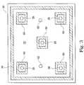
- FIG. 3illustrates an alternative embodiment of the present invention including a plurality of TSVs 28 and a plurality of cross-talk prevention rings 60 .
- Each of the TSVs 28may be encircled by one of the cross-talk prevention rings 60 , which are preferably formed simultaneously with seal rings 24 and 26 .
- cross-talk prevention rings 60are also formed of interconnected metal lines, vias, contact plugs, aluminum pads, and the like.
- An advantageous feature of this embodimentis that TSVs 28 may be embedded inside device region 32 .
- some of the TSVs 62are not expected to carry high currents and/or carry currents with high frequencies, these TSVs 62 do not necessarily need to be encircled by cross-talk prevention rings 60 .
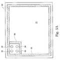
- FIG. 4illustrates a further embodiment, wherein TSVs 28 are enclosed by cross-talk prevention ring 66 , which is signal grounded. However, not all sides of cross-talk prevention ring 66 are adjacent to a respective edge 21 of semiconductor chip 20 . TSVs 28 and cross-talk prevention ring 66 may thus be formed at locations other than edge regions of semiconductor chip 20 .
- the cross-talk prevention structures of TSVs 28each include seal ring extension 68 and a portion of the rectangular-shaped seal ring 26 .
- Seal ring extension 68is preferably formed simultaneously, and thus has a similar layered structure, as seal ring 26 .
- This cross-talk prevention structuremay also isolate TSVs 28 from device region 32 .
- the cross-talk prevention structureis formed close to a corner of seal ring 26 .
- all TSVs 28are formed close to one edge of chip 20
- seal ring extension 68is formed as a straight line with two ends, each physically connected to a portion of seal ring 26 .
- cross-talk prevention ringsmay extend into the semiconductor substrates.
- conductive ring 70preferably formed of metal, is formed in semiconductor substrate 52 .
- Conductive ring 70is preferably a metal ring, which may be formed of tungsten, aluminum, copper, and the like.
- conductive ring 70is a well region, preferably heavily doped by implanting a p-type or n-type impurity.
- conductive ring 70adjoins cross-talk prevention ring 30 , and hence is also grounded.
- Conductive ring 70acts as a sink for currents generated by the cross-talk.
- a dielectric ring 72is formed in semiconductor substrate 52 .
- Dielectric ring 72acts as a barrier for the cross-talk currents generated in substrate 52 .
- the formation of conductive ring 70 or dielectric ring 72may include etching semiconductor substrate 52 to form a trench ring, filling the trench ring with a conductive material or a dielectric material, and performing a chemical mechanical polish to remove excess conductive/dielectric material.
- the conductive ring 70 or dielectric ring 72may also be formed under cross-talk prevention rings 60 and 66 as shown in FIGS. 3 and 4 , respectively, and under seal ring extensions 68 as shown in FIGS. 5A and 5B .
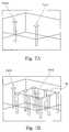
- FIG. 7Billustrates a structure for performing a simulation, wherein port 1 is a signal input port, and port 2 is a signal output port.
- the grounded cross-talk prevention ring 80encircles port 1 .
- the simulation results revealed that the scattering parameter S 21which is expressed as 20 log(V port — 2 /V port — 1 ), is significant reduced than if cross-talk prevention ring 80 does not exist, which structure is shown in FIG. 7A .
- the simulation resultsare shown in FIG. 8 , wherein the scattering parameter S 21 is illustrated as a function of frequency.
- Line 82is the simulation result of the structure shown in FIG.
- line 84is the simulation result of the structure shown in FIG. 7B . It may be concluded that the cross-talk are more severe at higher frequencies. However, regardless of the frequencies, the cross-talk prevention structure may reduce the cross-talk by more than about 20 decibels.
Landscapes
- Engineering & Computer Science (AREA)
- Physics & Mathematics (AREA)
- Microelectronics & Electronic Packaging (AREA)
- Power Engineering (AREA)
- Condensed Matter Physics & Semiconductors (AREA)
- General Physics & Mathematics (AREA)
- Computer Hardware Design (AREA)
- Health & Medical Sciences (AREA)
- Electromagnetism (AREA)
- Toxicology (AREA)
- Internal Circuitry In Semiconductor Integrated Circuit Devices (AREA)
- Semiconductor Integrated Circuits (AREA)
Abstract
Description
Claims (19)
Priority Applications (3)
| Application Number | Priority Date | Filing Date | Title |
|---|---|---|---|
| US11/945,022US8227902B2 (en) | 2007-11-26 | 2007-11-26 | Structures for preventing cross-talk between through-silicon vias and integrated circuits |
| CNA2008100969753ACN101447479A (en) | 2007-11-26 | 2008-05-12 | Structure for preventing crosstalk between through silicon via and integrated circuit |
| US13/346,995US8604594B2 (en) | 2007-11-26 | 2012-01-10 | Structures for preventing cross-talk between through-silicon vias and integrated circuits |
Applications Claiming Priority (1)
| Application Number | Priority Date | Filing Date | Title |
|---|---|---|---|
| US11/945,022US8227902B2 (en) | 2007-11-26 | 2007-11-26 | Structures for preventing cross-talk between through-silicon vias and integrated circuits |
Related Child Applications (1)
| Application Number | Title | Priority Date | Filing Date |
|---|---|---|---|
| US13/346,995ContinuationUS8604594B2 (en) | 2007-11-26 | 2012-01-10 | Structures for preventing cross-talk between through-silicon vias and integrated circuits |
Publications (2)
| Publication Number | Publication Date |
|---|---|
| US20090134500A1 US20090134500A1 (en) | 2009-05-28 |
| US8227902B2true US8227902B2 (en) | 2012-07-24 |
Family
ID=40668983
Family Applications (2)
| Application Number | Title | Priority Date | Filing Date |
|---|---|---|---|
| US11/945,022Active2029-03-27US8227902B2 (en) | 2007-11-26 | 2007-11-26 | Structures for preventing cross-talk between through-silicon vias and integrated circuits |
| US13/346,995Active2027-12-19US8604594B2 (en) | 2007-11-26 | 2012-01-10 | Structures for preventing cross-talk between through-silicon vias and integrated circuits |
Family Applications After (1)
| Application Number | Title | Priority Date | Filing Date |
|---|---|---|---|
| US13/346,995Active2027-12-19US8604594B2 (en) | 2007-11-26 | 2012-01-10 | Structures for preventing cross-talk between through-silicon vias and integrated circuits |
Country Status (2)
| Country | Link |
|---|---|
| US (2) | US8227902B2 (en) |
| CN (1) | CN101447479A (en) |
Cited By (71)
| Publication number | Priority date | Publication date | Assignee | Title |
|---|---|---|---|---|
| US20110266646A1 (en)* | 2010-01-15 | 2011-11-03 | Panasonic Corporation | Semiconductor device |
| US20130001793A1 (en)* | 2011-06-29 | 2013-01-03 | Globalfoundries Singapore Pte. Ltd. | Package interconnects |
| US20130015588A1 (en)* | 2007-11-14 | 2013-01-17 | Samsung Electronics Co., Ltd. | Semiconductor device having through electrode and method of fabricating the same |
| US20130140687A1 (en)* | 2011-12-06 | 2013-06-06 | Kabushiki Kaisha Toshiba | Semiconductor device |
| CN104347596A (en)* | 2013-08-08 | 2015-02-11 | 中芯国际集成电路制造(上海)有限公司 | Sealing ring structure of chip |
| US20150371956A1 (en)* | 2014-06-19 | 2015-12-24 | Globalfoundries Inc. | Crackstops for bulk semiconductor wafers |
| US9502272B2 (en) | 2014-12-29 | 2016-11-22 | Taiwan Semiconductor Manufacturing Company, Ltd. | Devices and methods of packaging semiconductor devices |
| US9520385B1 (en) | 2015-06-29 | 2016-12-13 | Taiwan Semiconductor Manufacturing Company, Ltd. | Package structure and method for forming same |
| US9536865B1 (en) | 2015-07-23 | 2017-01-03 | Taiwan Semiconductor Manufacturing Company, Ltd. | Interconnection joints having variable volumes in package structures and methods of formation thereof |
| US9570410B1 (en) | 2015-07-31 | 2017-02-14 | Taiwan Semiconductor Manufacturing Company, Ltd. | Methods of forming connector pad structures, interconnect structures, and structures thereof |
| US9570431B1 (en) | 2015-07-28 | 2017-02-14 | Taiwan Semiconductor Manufacturing Company, Ltd. | Semiconductor wafer for integrated packages |
| US9589941B1 (en) | 2016-01-15 | 2017-03-07 | Taiwan Semiconductor Manufacturing Company, Ltd. | Multi-chip package system and methods of forming the same |
| US9601410B2 (en) | 2015-01-07 | 2017-03-21 | Taiwan Semiconductor Manufacturing Company, Ltd. | Semiconductor device and method |
| US9633958B2 (en) | 2015-01-30 | 2017-04-25 | Taiwan Semiconductor Manufacturing Company, Ltd. | Bonding pad surface damage reduction in a formation of digital pattern generator |
| US9659878B2 (en) | 2015-10-20 | 2017-05-23 | Taiwan Semiconductor Manufacturing Company, Ltd. | Wafer level shielding in multi-stacked fan out packages and methods of forming same |
| US9659863B2 (en) | 2014-12-01 | 2017-05-23 | Taiwan Semiconductor Manufacturing Company, Ltd. | Semiconductor devices, multi-die packages, and methods of manufacture thereof |
| US9691695B2 (en) | 2015-08-31 | 2017-06-27 | Taiwan Semiconductor Manufacturing Company, Ltd. | Monolithic 3D integration inter-tier vias insertion scheme and associated layout structure |
| US9691723B2 (en) | 2015-10-30 | 2017-06-27 | Taiwan Semiconductor Manufacturing Company, Ltd. | Connector formation methods and packaged semiconductor devices |
| US9741669B2 (en) | 2016-01-26 | 2017-08-22 | Taiwan Semiconductor Manufacturing Company, Ltd. | Forming large chips through stitching |
| US9748212B2 (en) | 2015-04-30 | 2017-08-29 | Taiwan Semiconductor Manufacturing Company, Ltd. | Shadow pad for post-passivation interconnect structures |
| US9773757B2 (en) | 2016-01-19 | 2017-09-26 | Taiwan Semiconductor Manufacturing Company, Ltd. | Devices, packaged semiconductor devices, and semiconductor device packaging methods |
| US9786519B2 (en) | 2015-04-13 | 2017-10-10 | Taiwan Semiconductor Manufacturing Company, Ltd. | Packaged semiconductor devices and methods of packaging semiconductor devices |
| US9793246B1 (en) | 2016-05-31 | 2017-10-17 | Taiwan Semiconductor Manufacturing Co., Ltd. | Pop devices and methods of forming the same |
| US9812405B2 (en) | 2014-10-17 | 2017-11-07 | Taiwan Semiconductor Manufacturing Company Ltd. | Semiconductor package and manufacturing method of the same |
| US9818697B2 (en) | 2013-11-11 | 2017-11-14 | Taiwan Semiconductor Manufacturing Company Ltd. | Semiconductor package manufacturing method |
| US9842829B2 (en) | 2016-04-29 | 2017-12-12 | Taiwan Semiconductor Manufacturing Co., Ltd. | Chip package structure and method for forming the same |
| US9859258B2 (en) | 2016-05-17 | 2018-01-02 | Taiwan Semiconductor Manufacturing Company, Ltd. | Semiconductor device and method of manufacture |
| US9870975B1 (en) | 2016-07-14 | 2018-01-16 | Taiwan Semiconductor Manufacturing Co., Ltd. | Chip package with thermal dissipation structure and method for forming the same |
| US9875972B1 (en) | 2016-07-14 | 2018-01-23 | Taiwan Semiconductor Manufacturing Co., Ltd. | Semiconductor device structure and method for forming the same |
| US9875982B2 (en) | 2016-06-01 | 2018-01-23 | Taiwan Semiconductor Manufacturing Company Ltd | Semiconductor device and manufacturing method thereof |
| US9881903B2 (en) | 2016-05-31 | 2018-01-30 | Taiwan Semiconductor Manufacturing Company, Ltd. | Package-on-package structure with epoxy flux residue |
| US9893046B2 (en) | 2016-07-08 | 2018-02-13 | Taiwan Semiconductor Manufacturing Co., Ltd. | Thinning process using metal-assisted chemical etching |
| US9911623B2 (en) | 2015-12-15 | 2018-03-06 | Taiwan Semiconductor Manufacturing Company, Ltd. | Via connection to a partially filled trench |
| US9941186B2 (en) | 2016-06-30 | 2018-04-10 | Taiwan Semiconductor Manufacturing Company Ltd. | Method for manufacturing semiconductor structure |
| US9966360B2 (en) | 2016-07-05 | 2018-05-08 | Taiwan Semiconductor Manufacturing Co., Ltd. | Semiconductor package and manufacturing method thereof |
| US9969614B2 (en) | 2015-05-29 | 2018-05-15 | Taiwan Semiconductor Manufacturing Company, Ltd. | MEMS packages and methods of manufacture thereof |
| US10049981B2 (en) | 2016-09-08 | 2018-08-14 | Taiwan Semiconductor Manufacturing Company Ltd. | Through via structure, semiconductor device and manufacturing method thereof |
| US10050024B2 (en) | 2016-06-17 | 2018-08-14 | Taiwan Semiconductor Manufacturing Company Ltd. | Semiconductor package and manufacturing method of the same |
| US10050018B2 (en) | 2016-02-26 | 2018-08-14 | Taiwan Semiconductor Manufacturing Company, Ltd. | 3DIC structure and methods of forming |
| US10115675B2 (en) | 2016-06-28 | 2018-10-30 | Taiwan Semiconductor Manufacturing Co., Ltd. | Packaged semiconductor device and method of fabricating a packaged semiconductor device |
| US10120971B2 (en) | 2016-08-30 | 2018-11-06 | Taiwan Semiconductor Manufacturing Co., Ltd. | Integrated fan-out package and layout method thereof |
| US10147704B2 (en) | 2016-05-17 | 2018-12-04 | Taiwan Semiconductor Manufacturing Company, Ltd. | Semiconductor devices and methods of manufacturing thereof |
| US10153320B2 (en) | 2016-11-29 | 2018-12-11 | Taiwan Semiconductor Manufacturing Company Ltd. | Semiconductor device and method of forming the same |
| US10153218B2 (en) | 2016-11-29 | 2018-12-11 | Taiwan Semiconductor Manufacturing Company Ltd. | Semiconductor structure and manufacturing method thereof |
| US10157885B2 (en) | 2016-07-29 | 2018-12-18 | Taiwan Semiconductor Manufacturing Co., Ltd. | Package structure having magnetic bonding between substrates |
| US10163856B2 (en) | 2015-10-30 | 2018-12-25 | Taiwan Semiconductor Manufacturing Company, Ltd. | Stacked integrated circuit structure and method of forming |
| US10163709B2 (en) | 2015-02-13 | 2018-12-25 | Taiwan Semiconductor Manufacturing Company, Ltd. | Semiconductor device and method |
| US10163805B2 (en) | 2016-07-01 | 2018-12-25 | Taiwan Semiconductor Manufacturing Co., Ltd. | Package structure and method for forming the same |
| US10170444B2 (en) | 2015-06-30 | 2019-01-01 | Taiwan Semiconductor Manufacturing Company, Ltd. | Packages for semiconductor devices, packaged semiconductor devices, and methods of packaging semiconductor devices |
| US10170429B2 (en) | 2016-11-28 | 2019-01-01 | Taiwan Semiconductor Manufacturing Co., Ltd. | Method for forming package structure including intermetallic compound |
| US10229901B2 (en) | 2016-06-27 | 2019-03-12 | Taiwan Semiconductor Manufacturing Company, Ltd. | Immersion interconnections for semiconductor devices and methods of manufacture thereof |
| US10269732B2 (en) | 2016-07-20 | 2019-04-23 | Taiwan Semiconductor Manufacturing Company, Ltd. | Info package with integrated antennas or inductors |
| US10269682B2 (en) | 2015-10-09 | 2019-04-23 | Taiwan Semiconductor Manufacturing Company, Ltd. | Cooling devices, packaged semiconductor devices, and methods of packaging semiconductor devices |
| US10319701B2 (en) | 2015-01-07 | 2019-06-11 | Taiwan Semiconductor Manufacturing Company, Ltd. | Bonded 3D integrated circuit (3DIC) structure |
| US10332841B2 (en) | 2016-07-20 | 2019-06-25 | Taiwan Semiconductor Manufacturing Company, Ltd. | System on integrated chips and methods of forming the same |
| US10340258B2 (en) | 2015-04-30 | 2019-07-02 | Taiwan Semiconductor Manufacturing Company, Ltd. | Interconnect structures, packaged semiconductor devices, and methods of packaging semiconductor devices |
| US10475769B2 (en) | 2016-06-23 | 2019-11-12 | Taiwan Semiconductor Manufacturing Company Ltd. | Semiconductor package and manufacturing method of the same |
| US10497660B2 (en) | 2015-02-26 | 2019-12-03 | Taiwan Semiconductor Manufacturing Company, Ltd. | Interconnect structures, packaged semiconductor devices, and methods of packaging semiconductor devices |
| US10510605B2 (en) | 2016-07-29 | 2019-12-17 | Taiwan Semiconductor Manufacturing Company, Ltd. | Semiconductor die singulation and structures formed thereby |
| US10535632B2 (en) | 2016-09-02 | 2020-01-14 | Taiwan Semiconductor Manufacturing Company Ltd. | Semiconductor package structure and method of manufacturing the same |
| US10644229B2 (en) | 2015-09-18 | 2020-05-05 | Taiwan Semiconductor Manufacturing Company, Ltd. | Magnetoresistive random access memory cell and fabricating the same |
| US10685911B2 (en) | 2016-06-30 | 2020-06-16 | Taiwan Semiconductor Manufacturing Company Ltd. | Semiconductor package and manufacturing method of the same |
| US10879183B2 (en) | 2018-06-22 | 2020-12-29 | Taiwan Semiconductor Manufacturing Company, Ltd. | Semiconductor device and method of manufacture |
| US11133304B2 (en) | 2019-11-27 | 2021-09-28 | Taiwan Semiconductor Manufacturing Co., Ltd. | Packaging scheme involving metal-insulator-metal capacitor |
| US11172142B2 (en) | 2018-09-25 | 2021-11-09 | Taiwan Semiconductor Manufacturing Co., Ltd. | Image sensor for sensing LED light with reduced flickering |
| US11201122B2 (en) | 2018-09-27 | 2021-12-14 | Taiwan Semiconductor Manufacturing Co., Ltd. | Method of fabricating semiconductor device with reduced warpage and better trench filling performance |
| US11257741B2 (en) | 2019-05-28 | 2022-02-22 | Samsung Electronics Co., Ltd. | Semiconductor package |
| US20230008633A1 (en)* | 2021-07-08 | 2023-01-12 | Changxin Memory Technologies, Inc. | Semiconductor structure and method for forming semiconductor structure |
| US11990390B2 (en) | 2020-07-06 | 2024-05-21 | Changxin Memory Technologies, Inc. | Semiconductor structure |
| US12412790B2 (en) | 2021-09-14 | 2025-09-09 | Changxin Memory Technologies, Inc. | Semiconductor structure, memory, and crack testing method |
| US12424558B2 (en) | 2022-08-12 | 2025-09-23 | Taiwan Semiconductor Manufacturing Company, Ltd. | Bridge die having different surface orientation than IC dies interconnected by the bridge die |
Families Citing this family (67)
| Publication number | Priority date | Publication date | Assignee | Title |
|---|---|---|---|---|
| US8053902B2 (en)* | 2008-12-02 | 2011-11-08 | Taiwan Semiconductor Manufacturing Company, Ltd. | Isolation structure for protecting dielectric layers from degradation |
| US8227889B2 (en)* | 2008-12-08 | 2012-07-24 | United Microelectronics Corp. | Semiconductor device |
| US8168529B2 (en)* | 2009-01-26 | 2012-05-01 | Taiwan Semiconductor Manufacturing Company, Ltd. | Forming seal ring in an integrated circuit die |
| KR101053531B1 (en)* | 2009-09-30 | 2011-08-03 | 주식회사 하이닉스반도체 | Semiconductor device and calibration method thereof |
| KR101038996B1 (en)* | 2009-11-30 | 2011-06-03 | 주식회사 하이닉스반도체 | Repair circuit and semiconductor device including the same |
| US8304286B2 (en)* | 2009-12-11 | 2012-11-06 | Stats Chippac Ltd. | Integrated circuit packaging system with shielded package and method of manufacture thereof |
| KR101069725B1 (en)* | 2009-12-24 | 2011-10-04 | 주식회사 하이닉스반도체 | Semiconductor Memory Apparatus, Control Circuit and Method for Fault Address Therefor |
| KR101153796B1 (en)* | 2009-12-24 | 2012-06-14 | 에스케이하이닉스 주식회사 | Repair circuit and repair method of semiconductor apparatus |
| KR101103064B1 (en)* | 2010-01-29 | 2012-01-06 | 주식회사 하이닉스반도체 | Semiconductor devices |
| KR20110097095A (en)* | 2010-02-24 | 2011-08-31 | 주식회사 하이닉스반도체 | Redundancy data storage circuit, redundancy data control method and repair determination circuit of semiconductor memory |
| KR101143443B1 (en)* | 2010-03-29 | 2012-05-23 | 에스케이하이닉스 주식회사 | Semiconductor apparatus and its repairing method |
| KR101033491B1 (en) | 2010-03-31 | 2011-05-09 | 주식회사 하이닉스반도체 | Semiconductor devices |
| US9293366B2 (en)* | 2010-04-28 | 2016-03-22 | Taiwan Semiconductor Manufacturing Company, Ltd. | Through-substrate vias with improved connections |
| KR101124331B1 (en) | 2010-04-30 | 2012-03-19 | 주식회사 하이닉스반도체 | Semiconductor Apparatus |
| US9018768B2 (en)* | 2010-06-28 | 2015-04-28 | Samsung Electronics Co., Ltd. | Integrated circuit having through silicon via structure with minimized deterioration |
| US8193039B2 (en) | 2010-09-24 | 2012-06-05 | Advanced Micro Devices, Inc. | Semiconductor chip with reinforcing through-silicon-vias |
| CN102024782B (en)* | 2010-10-12 | 2012-07-25 | 北京大学 | Three-dimensional vertical interconnecting structure and manufacturing method thereof |
| US8227840B2 (en)* | 2010-11-24 | 2012-07-24 | Nanya Technology Corp. | Integrated circuit device and method of forming the same |
| US9460840B2 (en) | 2011-03-03 | 2016-10-04 | Skyworks Solutions, Inc. | Seal ring inductor and method of forming the same |
| US8791015B2 (en)* | 2011-04-30 | 2014-07-29 | Stats Chippac, Ltd. | Semiconductor device and method of forming shielding layer over active surface of semiconductor die |
| US8487447B2 (en)* | 2011-05-19 | 2013-07-16 | International Business Machines Corporation | Semiconductor structure having offset passivation to reduce electromigration |
| US8779553B2 (en)* | 2011-06-16 | 2014-07-15 | Xilinx, Inc. | Stress-aware design for integrated circuits comprising a stress inducing structure and keep out zone |
| US8618640B2 (en) | 2011-07-29 | 2013-12-31 | Taiwan Semiconductor Manufacturing Company, Ltd. | Method of shielding through silicon vias in a passive interposer |
| US8546953B2 (en) | 2011-12-13 | 2013-10-01 | Taiwan Semiconductor Manufacturing Co., Ltd. | Through silicon via (TSV) isolation structures for noise reduction in 3D integrated circuit |
| WO2013100897A1 (en)* | 2011-12-27 | 2013-07-04 | Intel Corporation | Damage monitor structure for through-silicon via (tsv) arrays |
| JP2013143532A (en)* | 2012-01-12 | 2013-07-22 | Toshiba Corp | Semiconductor device |
| TW201403782A (en) | 2012-07-04 | 2014-01-16 | Ind Tech Res Inst | Method for manufacturing through substrate via structure, through substrate via structure and control method of TSV capacitance |
| US9923101B2 (en) | 2012-09-13 | 2018-03-20 | Taiwan Semiconductor Manufacturing Co., Ltd. | Semiconductor structure |
| CN102832178A (en)* | 2012-09-18 | 2012-12-19 | 上海工程技术大学 | Sealing ring structure used for integrated circuit chip |
| US9490190B2 (en) | 2012-09-21 | 2016-11-08 | Taiwan Semiconductor Manufacturing Company, Ltd. | Thermal dissipation through seal rings in 3DIC structure |
| US9219038B2 (en)* | 2013-03-12 | 2015-12-22 | Taiwan Semiconductor Manufacturing Co., Ltd. | Shielding for through-silicon-via |
| US9640456B2 (en)* | 2013-03-15 | 2017-05-02 | Taiwan Semiconductor Manufacturing Company Limited | Support structure for integrated circuitry |
| KR102177702B1 (en) | 2014-02-03 | 2020-11-11 | 삼성전자주식회사 | Via Structures and Semiconductor Devices Having a Via plug |
| US9530739B2 (en) | 2014-12-15 | 2016-12-27 | Qualcomm Incorporated | Package on package (PoP) device comprising a high performance inter package connection |
| CN104793120B (en)* | 2015-04-03 | 2017-06-30 | 浙江大学 | The measurement structure of silicon hole electrical characteristics is measured based on De- embedding method |
| US10373865B2 (en)* | 2015-07-24 | 2019-08-06 | Taiwan Semiconductor Manufacturing Company Limited | Semiconductor device and manufacturing method thereof |
| US9881881B2 (en)* | 2015-07-24 | 2018-01-30 | Qualcomm Incorporated | Conductive seal ring for power bus distribution |
| WO2017052472A1 (en)* | 2015-09-22 | 2017-03-30 | Agency For Science, Technology And Research | Semiconductor device and method of forming the same |
| CN105336727B (en)* | 2015-10-13 | 2017-10-17 | 北京信息科技大学 | A kind of benzenoid form substrate through-hole transmission structure and substrate through-hole vertical transfer structure |
| US9698108B1 (en)* | 2015-12-23 | 2017-07-04 | Intel Corporation | Structures to mitigate contamination on a back side of a semiconductor substrate |
| US9793227B1 (en)* | 2016-04-21 | 2017-10-17 | Peregrine Semiconductor San Diego | Switchable die seal connection |
| US10854568B2 (en) | 2017-04-07 | 2020-12-01 | Taiwan Semiconductor Manufacturing Company, Ltd. | Packages with Si-substrate-free interposer and method forming same |
| DE102017124104B4 (en) | 2017-04-07 | 2025-05-15 | Taiwan Semiconductor Manufacturing Co., Ltd. | Packages with Si-substrate-free interposer and methods for forming the same |
| US10522449B2 (en) | 2017-04-10 | 2019-12-31 | Taiwan Semiconductor Manufacturing Company, Ltd. | Packages with Si-substrate-free interposer and method forming same |
| DE102017123449B4 (en) | 2017-04-10 | 2023-12-28 | Taiwan Semiconductor Manufacturing Co. Ltd. | Housing with Si-substrate-free intermediate piece and training process |
| US10170432B2 (en) | 2017-04-20 | 2019-01-01 | Nanya Technology Corporation | Semiconductor structure |
| JP2017147475A (en)* | 2017-06-06 | 2017-08-24 | ルネサスエレクトロニクス株式会社 | Semiconductor device |
| US10290571B2 (en) | 2017-09-18 | 2019-05-14 | Taiwan Semiconductor Manufacturing Company, Ltd. | Packages with si-substrate-free interposer and method forming same |
| US11296031B2 (en)* | 2018-03-30 | 2022-04-05 | Intel Corporation | Dielectric-filled trench isolation of vias |
| US10629592B2 (en)* | 2018-05-25 | 2020-04-21 | Taiwan Semiconductor Manufacturing Co., Ltd. | Through silicon via design for stacking integrated circuits |
| US11756977B2 (en) | 2018-06-21 | 2023-09-12 | Semiconductor Components Industries, Llc | Backside illumination image sensors |
| US10504852B1 (en)* | 2018-06-25 | 2019-12-10 | Taiwan Semiconductor Manufacturing Co., Ltd. | Three-dimensional integrated circuit structures |
| US10734285B2 (en)* | 2018-06-28 | 2020-08-04 | Taiwan Semiconductor Manufacturing Co., Ltd. | Bonding support structure (and related process) for wafer stacking |
| US11557545B2 (en)* | 2018-12-04 | 2023-01-17 | Qorvo Us, Inc. | Monolithic microwave integrated circuit (MMIC) with embedded transmission line (ETL) ground shielding |
| US10825692B2 (en) | 2018-12-20 | 2020-11-03 | Advanced Micro Devices, Inc. | Semiconductor chip gettering |
| US11088094B2 (en)* | 2019-05-31 | 2021-08-10 | Taiwan Semiconductor Manufacturing Company, Ltd. | Air channel formation in packaging process |
| US11456247B2 (en)* | 2019-06-13 | 2022-09-27 | Nanya Technology Corporation | Semiconductor device and fabrication method for the same |
| US20210035918A1 (en)* | 2019-07-31 | 2021-02-04 | Nanya Technology Corporation | Semiconductor structure and fabrication method thereof |
| KR102834550B1 (en)* | 2020-06-30 | 2025-07-14 | 삼성전자주식회사 | Integrated circuit device and semiconductor package including the same |
| CN113903724B (en)* | 2020-07-06 | 2023-03-24 | 长鑫存储技术有限公司 | Semiconductor structure |
| CN114188311A (en)* | 2020-09-15 | 2022-03-15 | 联华电子股份有限公司 | Semiconductor structure |
| CN112510001B (en)* | 2020-11-30 | 2023-06-30 | 珠海天成先进半导体科技有限公司 | Chip structure with TSV through holes and preparation method |
| US20220199546A1 (en)* | 2020-12-18 | 2022-06-23 | Intel Corporation | Shield structures in microelectronic assemblies having direct bonding |
| US11682652B2 (en)* | 2021-03-10 | 2023-06-20 | Taiwan Semiconductor Manufacturing Company, Ltd. | Notched wafer and bonding support structure to improve wafer stacking |
| US12136600B2 (en)* | 2021-04-08 | 2024-11-05 | Taiwan Semiconductor Manufacturing Company, Ltd. | Grounded metal ring structure for through-silicon via |
| US12165969B2 (en)* | 2021-06-09 | 2024-12-10 | Taiwan Semiconductor Manufacturing Company, Ltd. | Integrated circuit device and method |
| CN115810612B (en)* | 2021-09-14 | 2025-07-25 | 长鑫存储技术有限公司 | Semiconductor structure, memory and crack testing method |
Citations (49)
| Publication number | Priority date | Publication date | Assignee | Title |
|---|---|---|---|---|
| US5391917A (en) | 1993-05-10 | 1995-02-21 | International Business Machines Corporation | Multiprocessor module packaging |
| US5510298A (en) | 1991-09-12 | 1996-04-23 | Texas Instruments Incorporated | Method of interconnect in an integrated circuit |
| US5767001A (en) | 1993-05-05 | 1998-06-16 | Siemens Aktiengesellschaft | Process for producing semiconductor components between which contact is made vertically |
| US5924289A (en)* | 1997-07-01 | 1999-07-20 | Medical Products, Inc. | Controlled temperature cabinet system and method |
| US5998292A (en) | 1997-11-12 | 1999-12-07 | International Business Machines Corporation | Method for making three dimensional circuit integration |
| US6116674A (en)* | 1997-09-05 | 2000-09-12 | Ford Motor Company | Removable console for use with a vehicle |
| US6184060B1 (en) | 1996-10-29 | 2001-02-06 | Trusi Technologies Llc | Integrated circuits and methods for their fabrication |
| US6322903B1 (en) | 1999-12-06 | 2001-11-27 | Tru-Si Technologies, Inc. | Package of integrated circuits and vertical integration |
| US6448168B1 (en) | 1997-09-30 | 2002-09-10 | Intel Corporation | Method for distributing a clock on the silicon backside of an integrated circuit |
| US6465892B1 (en) | 1999-04-13 | 2002-10-15 | Oki Electric Industry Co., Ltd. | Interconnect structure for stacked semiconductor device |
| US6478204B2 (en)* | 1998-05-29 | 2002-11-12 | Carsten Lange | Receptacle cover |
| US6538333B2 (en) | 2000-06-16 | 2003-03-25 | Chartered Semiconductor Manufacturing Ltd. | Three dimensional IC package module |
| US6547326B1 (en)* | 2001-11-01 | 2003-04-15 | Ford Global Technologies, Inc. | Automotive seat flip-out cupholder |
| US6563181B1 (en)* | 2001-11-02 | 2003-05-13 | Motorola, Inc. | High frequency signal isolation in a semiconductor device |
| US6599778B2 (en) | 2001-12-19 | 2003-07-29 | International Business Machines Corporation | Chip and wafer integration process using vertical connections |
| US6664129B2 (en) | 1996-10-29 | 2003-12-16 | Tri-Si Technologies, Inc. | Integrated circuits and methods for their fabrication |
| US20040080173A1 (en)* | 2002-07-11 | 2004-04-29 | Kenji Niwa | Console box |
| US6761388B2 (en)* | 2002-01-08 | 2004-07-13 | Plastech Engineered Products | Console system having a double-hinged lid |
| US20040150070A1 (en) | 2003-02-03 | 2004-08-05 | Nec Electronics Corporation | Semiconductor device and method for manufacturing the same |
| CN1532924A (en) | 2003-03-25 | 2004-09-29 | ���ǵ�����ʽ���� | Wafer-level packaging, multi-package stacking, and manufacturing method thereof |
| US6800930B2 (en) | 2002-07-31 | 2004-10-05 | Micron Technology, Inc. | Semiconductor dice having back side redistribution layer accessed using through-silicon vias, and assemblies |
| US6841883B1 (en) | 2003-03-31 | 2005-01-11 | Micron Technology, Inc. | Multi-dice chip scale semiconductor components and wafer level methods of fabrication |
| US6924551B2 (en) | 2003-05-28 | 2005-08-02 | Intel Corporation | Through silicon via, folded flex microelectronic package |
| US6962872B2 (en) | 2002-12-09 | 2005-11-08 | International Business Machines Corporation | High density chip carrier with integrated passive devices |
| US7049170B2 (en) | 2003-12-17 | 2006-05-23 | Tru-Si Technologies, Inc. | Integrated circuits and packaging substrates with cavities, and attachment methods including insertion of protruding contact pads into cavities |
| US7060601B2 (en) | 2003-12-17 | 2006-06-13 | Tru-Si Technologies, Inc. | Packaging substrates for integrated circuits and soldering methods |
| US20060141653A1 (en) | 2004-12-23 | 2006-06-29 | Ja-Young Choi | Methods of manufacturing an image device |
| US7071546B2 (en) | 2002-01-16 | 2006-07-04 | Alfred E. Mann Foundation For Scientific Research | Space-saving packaging of electronic circuits |
| US7111149B2 (en) | 2003-07-07 | 2006-09-19 | Intel Corporation | Method and apparatus for generating a device ID for stacked devices |
| US7122912B2 (en) | 2004-01-28 | 2006-10-17 | Nec Electronics Corporation | Chip and multi-chip semiconductor device using thereof and method for manufacturing same |
| CN1858909A (en) | 2005-05-02 | 2006-11-08 | 台湾积体电路制造股份有限公司 | Integrated circuit structure |
| US7157787B2 (en) | 2002-02-20 | 2007-01-02 | Intel Corporation | Process of vertically stacking multiple wafers supporting different active integrated circuit (IC) devices |
| US7193308B2 (en) | 2003-09-26 | 2007-03-20 | Seiko Epson Corporation | Intermediate chip module, semiconductor device, circuit board, and electronic device |
| US20070075559A1 (en)* | 2005-10-03 | 2007-04-05 | Lear Corporation | Console assembly having integrated media storage |
| US7224060B2 (en) | 2004-01-30 | 2007-05-29 | Chartered Semiconductor Manufacturing Ltd. | Integrated circuit with protective moat |
| US20070119885A1 (en)* | 2005-11-28 | 2007-05-31 | Toyoda Gosei Co. Ltd. | Floor console with reconfigurable storage |
| US20070152461A1 (en)* | 2005-12-29 | 2007-07-05 | Lear Corporation | Console assembly for a vehicle |
| US7240814B2 (en)* | 2004-03-25 | 2007-07-10 | Honda Motor Co., Ltd. | Vehicle center console defining a reconfigurable storage area |
| US7262495B2 (en) | 2004-10-07 | 2007-08-28 | Hewlett-Packard Development Company, L.P. | 3D interconnect with protruding contacts |
| US20070246960A1 (en)* | 2006-04-20 | 2007-10-25 | Johnson Controls Technology Company | Latch system for sliding panel in vehicle |
| US7297574B2 (en) | 2005-06-17 | 2007-11-20 | Infineon Technologies Ag | Multi-chip device and method for producing a multi-chip device |
| US7335972B2 (en) | 2003-11-13 | 2008-02-26 | Sandia Corporation | Heterogeneously integrated microsystem-on-a-chip |
| US7427803B2 (en)* | 2006-09-22 | 2008-09-23 | Taiwan Semiconductor Manufacturing Company, Ltd. | Electromagnetic shielding using through-silicon vias |
| US20080283959A1 (en) | 2007-05-16 | 2008-11-20 | Chen-Shien Chen | Tapered through-silicon via structure |
| US20090072568A1 (en)* | 2007-09-19 | 2009-03-19 | Honda Motor Co., Ltd. | Sliding lid guard |
| US20090127652A1 (en)* | 2007-11-20 | 2009-05-21 | Hanyi Ding | Structure of very high insertion loss of the substrate noise decoupling |
| US20090191708A1 (en) | 2008-01-30 | 2009-07-30 | Kropewnicki Thomas J | Method for forming a through silicon via layout |
| US7701057B1 (en)* | 2007-04-25 | 2010-04-20 | Xilinx, Inc. | Semiconductor device having structures for reducing substrate noise coupled from through die vias |
| US20100133696A1 (en) | 2008-12-02 | 2010-06-03 | Ming-Fa Chen | Isolation Structure for Protecting Dielectric Layers from Degradation |
Family Cites Families (2)
| Publication number | Priority date | Publication date | Assignee | Title |
|---|---|---|---|---|
| US6565181B2 (en) | 1997-07-12 | 2003-05-20 | Silverbrook Research Pty Ltd | Printing cartridge with switch array identification |
| CN1617312A (en)* | 2003-11-10 | 2005-05-18 | 松下电器产业株式会社 | Semiconductor device and manufacturing method thereof |
- 2007
- 2007-11-26USUS11/945,022patent/US8227902B2/enactiveActive
- 2008
- 2008-05-12CNCNA2008100969753Apatent/CN101447479A/enactivePending
- 2012
- 2012-01-10USUS13/346,995patent/US8604594B2/enactiveActive
Patent Citations (59)
| Publication number | Priority date | Publication date | Assignee | Title |
|---|---|---|---|---|
| US5510298A (en) | 1991-09-12 | 1996-04-23 | Texas Instruments Incorporated | Method of interconnect in an integrated circuit |
| US5767001A (en) | 1993-05-05 | 1998-06-16 | Siemens Aktiengesellschaft | Process for producing semiconductor components between which contact is made vertically |
| US5391917A (en) | 1993-05-10 | 1995-02-21 | International Business Machines Corporation | Multiprocessor module packaging |
| US6740582B2 (en) | 1996-10-29 | 2004-05-25 | Tru-Si Technologies, Inc. | Integrated circuits and methods for their fabrication |
| US6184060B1 (en) | 1996-10-29 | 2001-02-06 | Trusi Technologies Llc | Integrated circuits and methods for their fabrication |
| US6664129B2 (en) | 1996-10-29 | 2003-12-16 | Tri-Si Technologies, Inc. | Integrated circuits and methods for their fabrication |
| US6639303B2 (en) | 1996-10-29 | 2003-10-28 | Tru-Si Technolgies, Inc. | Integrated circuits and methods for their fabrication |
| US6882030B2 (en) | 1996-10-29 | 2005-04-19 | Tru-Si Technologies, Inc. | Integrated circuit structures with a conductor formed in a through hole in a semiconductor substrate and protruding from a surface of the substrate |
| US5924289A (en)* | 1997-07-01 | 1999-07-20 | Medical Products, Inc. | Controlled temperature cabinet system and method |
| US6116674A (en)* | 1997-09-05 | 2000-09-12 | Ford Motor Company | Removable console for use with a vehicle |
| US6448168B1 (en) | 1997-09-30 | 2002-09-10 | Intel Corporation | Method for distributing a clock on the silicon backside of an integrated circuit |
| US5998292A (en) | 1997-11-12 | 1999-12-07 | International Business Machines Corporation | Method for making three dimensional circuit integration |
| US6478204B2 (en)* | 1998-05-29 | 2002-11-12 | Carsten Lange | Receptacle cover |
| US6472293B2 (en) | 1999-04-13 | 2002-10-29 | Oki Electric Industry Co., Ltd. | Method for manufacturing an interconnect structure for stacked semiconductor device |
| US6465892B1 (en) | 1999-04-13 | 2002-10-15 | Oki Electric Industry Co., Ltd. | Interconnect structure for stacked semiconductor device |
| US6322903B1 (en) | 1999-12-06 | 2001-11-27 | Tru-Si Technologies, Inc. | Package of integrated circuits and vertical integration |
| US6693361B1 (en) | 1999-12-06 | 2004-02-17 | Tru-Si Technologies, Inc. | Packaging of integrated circuits and vertical integration |
| US6538333B2 (en) | 2000-06-16 | 2003-03-25 | Chartered Semiconductor Manufacturing Ltd. | Three dimensional IC package module |
| US6547326B1 (en)* | 2001-11-01 | 2003-04-15 | Ford Global Technologies, Inc. | Automotive seat flip-out cupholder |
| US6563181B1 (en)* | 2001-11-02 | 2003-05-13 | Motorola, Inc. | High frequency signal isolation in a semiconductor device |
| US6599778B2 (en) | 2001-12-19 | 2003-07-29 | International Business Machines Corporation | Chip and wafer integration process using vertical connections |
| US6761388B2 (en)* | 2002-01-08 | 2004-07-13 | Plastech Engineered Products | Console system having a double-hinged lid |
| US7071546B2 (en) | 2002-01-16 | 2006-07-04 | Alfred E. Mann Foundation For Scientific Research | Space-saving packaging of electronic circuits |
| US7157787B2 (en) | 2002-02-20 | 2007-01-02 | Intel Corporation | Process of vertically stacking multiple wafers supporting different active integrated circuit (IC) devices |
| US20040080173A1 (en)* | 2002-07-11 | 2004-04-29 | Kenji Niwa | Console box |
| US7355273B2 (en) | 2002-07-31 | 2008-04-08 | Micron Technology, Inc. | Semiconductor dice having back side redistribution layer accessed using through-silicon vias, methods |
| US6800930B2 (en) | 2002-07-31 | 2004-10-05 | Micron Technology, Inc. | Semiconductor dice having back side redistribution layer accessed using through-silicon vias, and assemblies |
| US6962867B2 (en) | 2002-07-31 | 2005-11-08 | Microntechnology, Inc. | Methods of fabrication of semiconductor dice having back side redistribution layer accessed using through-silicon vias and assemblies thereof |
| US6962872B2 (en) | 2002-12-09 | 2005-11-08 | International Business Machines Corporation | High density chip carrier with integrated passive devices |
| US7030481B2 (en) | 2002-12-09 | 2006-04-18 | Internation Business Machines Corporation | High density chip carrier with integrated passive devices |
| US20040150070A1 (en) | 2003-02-03 | 2004-08-05 | Nec Electronics Corporation | Semiconductor device and method for manufacturing the same |
| US7335592B2 (en) | 2003-03-25 | 2008-02-26 | Samsung Electronics Co., Ltd. | Wafer level package, multi-package stack, and method of manufacturing the same |
| CN1532924A (en) | 2003-03-25 | 2004-09-29 | ���ǵ�����ʽ���� | Wafer-level packaging, multi-package stacking, and manufacturing method thereof |
| US6841883B1 (en) | 2003-03-31 | 2005-01-11 | Micron Technology, Inc. | Multi-dice chip scale semiconductor components and wafer level methods of fabrication |
| US6924551B2 (en) | 2003-05-28 | 2005-08-02 | Intel Corporation | Through silicon via, folded flex microelectronic package |
| US7111149B2 (en) | 2003-07-07 | 2006-09-19 | Intel Corporation | Method and apparatus for generating a device ID for stacked devices |
| US7193308B2 (en) | 2003-09-26 | 2007-03-20 | Seiko Epson Corporation | Intermediate chip module, semiconductor device, circuit board, and electronic device |
| US7335972B2 (en) | 2003-11-13 | 2008-02-26 | Sandia Corporation | Heterogeneously integrated microsystem-on-a-chip |
| US7049170B2 (en) | 2003-12-17 | 2006-05-23 | Tru-Si Technologies, Inc. | Integrated circuits and packaging substrates with cavities, and attachment methods including insertion of protruding contact pads into cavities |
| US7060601B2 (en) | 2003-12-17 | 2006-06-13 | Tru-Si Technologies, Inc. | Packaging substrates for integrated circuits and soldering methods |
| US7122912B2 (en) | 2004-01-28 | 2006-10-17 | Nec Electronics Corporation | Chip and multi-chip semiconductor device using thereof and method for manufacturing same |
| US7224060B2 (en) | 2004-01-30 | 2007-05-29 | Chartered Semiconductor Manufacturing Ltd. | Integrated circuit with protective moat |
| US7240814B2 (en)* | 2004-03-25 | 2007-07-10 | Honda Motor Co., Ltd. | Vehicle center console defining a reconfigurable storage area |
| US7262495B2 (en) | 2004-10-07 | 2007-08-28 | Hewlett-Packard Development Company, L.P. | 3D interconnect with protruding contacts |
| US20060141653A1 (en) | 2004-12-23 | 2006-06-29 | Ja-Young Choi | Methods of manufacturing an image device |
| CN1858909A (en) | 2005-05-02 | 2006-11-08 | 台湾积体电路制造股份有限公司 | Integrated circuit structure |
| US7615841B2 (en) | 2005-05-02 | 2009-11-10 | Taiwan Semiconductor Manufacturing Company, Ltd. | Design structure for coupling noise prevention |
| US7297574B2 (en) | 2005-06-17 | 2007-11-20 | Infineon Technologies Ag | Multi-chip device and method for producing a multi-chip device |
| US20070075559A1 (en)* | 2005-10-03 | 2007-04-05 | Lear Corporation | Console assembly having integrated media storage |
| US20070119885A1 (en)* | 2005-11-28 | 2007-05-31 | Toyoda Gosei Co. Ltd. | Floor console with reconfigurable storage |
| US20070152461A1 (en)* | 2005-12-29 | 2007-07-05 | Lear Corporation | Console assembly for a vehicle |
| US20070246960A1 (en)* | 2006-04-20 | 2007-10-25 | Johnson Controls Technology Company | Latch system for sliding panel in vehicle |
| US7427803B2 (en)* | 2006-09-22 | 2008-09-23 | Taiwan Semiconductor Manufacturing Company, Ltd. | Electromagnetic shielding using through-silicon vias |
| US7701057B1 (en)* | 2007-04-25 | 2010-04-20 | Xilinx, Inc. | Semiconductor device having structures for reducing substrate noise coupled from through die vias |
| US20080283959A1 (en) | 2007-05-16 | 2008-11-20 | Chen-Shien Chen | Tapered through-silicon via structure |
| US20090072568A1 (en)* | 2007-09-19 | 2009-03-19 | Honda Motor Co., Ltd. | Sliding lid guard |
| US20090127652A1 (en)* | 2007-11-20 | 2009-05-21 | Hanyi Ding | Structure of very high insertion loss of the substrate noise decoupling |
| US20090191708A1 (en) | 2008-01-30 | 2009-07-30 | Kropewnicki Thomas J | Method for forming a through silicon via layout |
| US20100133696A1 (en) | 2008-12-02 | 2010-06-03 | Ming-Fa Chen | Isolation Structure for Protecting Dielectric Layers from Degradation |
Cited By (132)
| Publication number | Priority date | Publication date | Assignee | Title |
|---|---|---|---|---|
| US8659163B2 (en)* | 2007-11-14 | 2014-02-25 | Samsung Electronics Co., Ltd. | Semiconductor device having through electrode and method of fabricating the same |
| US9041218B2 (en)* | 2007-11-14 | 2015-05-26 | Samsung Electronics Co., Ltd. | Semiconductor device having through electrode and method of fabricating the same |
| US20130015588A1 (en)* | 2007-11-14 | 2013-01-17 | Samsung Electronics Co., Ltd. | Semiconductor device having through electrode and method of fabricating the same |
| US20140167289A1 (en)* | 2007-11-14 | 2014-06-19 | Samsung Electronics Co., Ltd. | Semiconductor device having through electrode and method of fabricating the same |
| US20110266646A1 (en)* | 2010-01-15 | 2011-11-03 | Panasonic Corporation | Semiconductor device |
| US8450836B2 (en)* | 2010-01-15 | 2013-05-28 | Panasonic Corporation | Semiconductor device |
| US8883634B2 (en)* | 2011-06-29 | 2014-11-11 | Globalfoundries Singapore Pte. Ltd. | Package interconnects |
| US20150061085A1 (en)* | 2011-06-29 | 2015-03-05 | Globalfoundries Singapore Pte Ltd. | Package interconnects |
| US20130001793A1 (en)* | 2011-06-29 | 2013-01-03 | Globalfoundries Singapore Pte. Ltd. | Package interconnects |
| US20130140687A1 (en)* | 2011-12-06 | 2013-06-06 | Kabushiki Kaisha Toshiba | Semiconductor device |
| US8558390B2 (en)* | 2011-12-06 | 2013-10-15 | Kabushiki Kaisha Toshiba | Semiconductor device |
| CN104347596B (en)* | 2013-08-08 | 2017-02-08 | 中芯国际集成电路制造(上海)有限公司 | Sealing ring structure of chip |
| CN104347596A (en)* | 2013-08-08 | 2015-02-11 | 中芯国际集成电路制造(上海)有限公司 | Sealing ring structure of chip |
| US9818697B2 (en) | 2013-11-11 | 2017-11-14 | Taiwan Semiconductor Manufacturing Company Ltd. | Semiconductor package manufacturing method |
| US20150371956A1 (en)* | 2014-06-19 | 2015-12-24 | Globalfoundries Inc. | Crackstops for bulk semiconductor wafers |
| US9812405B2 (en) | 2014-10-17 | 2017-11-07 | Taiwan Semiconductor Manufacturing Company Ltd. | Semiconductor package and manufacturing method of the same |
| US9659863B2 (en) | 2014-12-01 | 2017-05-23 | Taiwan Semiconductor Manufacturing Company, Ltd. | Semiconductor devices, multi-die packages, and methods of manufacture thereof |
| US9984969B2 (en) | 2014-12-01 | 2018-05-29 | Taiwan Semiconductor Manufacturing Company, Ltd. | Semiconductor devices, multi-die packages, and methods of manufacure thereof |
| US9502272B2 (en) | 2014-12-29 | 2016-11-22 | Taiwan Semiconductor Manufacturing Company, Ltd. | Devices and methods of packaging semiconductor devices |
| US9935084B2 (en) | 2014-12-29 | 2018-04-03 | Taiwan Semiconductor Manufacturing Company | Devices and methods of packaging semiconductor devices |
| US9601410B2 (en) | 2015-01-07 | 2017-03-21 | Taiwan Semiconductor Manufacturing Company, Ltd. | Semiconductor device and method |
| US10319701B2 (en) | 2015-01-07 | 2019-06-11 | Taiwan Semiconductor Manufacturing Company, Ltd. | Bonded 3D integrated circuit (3DIC) structure |
| US10269761B2 (en) | 2015-01-07 | 2019-04-23 | Taiwan Semiconductor Manufacturing Company, Ltd. | Semiconductor device and method |
| US11239201B2 (en) | 2015-01-07 | 2022-02-01 | Taiwan Semiconductor Manufacturing Company, Ltd. | 3D integrated circuit (3DIC) structure |
| US12418001B2 (en) | 2015-01-07 | 2025-09-16 | Taiwan Semiconductor Manufacturing Company, Ltd. | 3D integrated circuit (3DIC) structure |
| US9633958B2 (en) | 2015-01-30 | 2017-04-25 | Taiwan Semiconductor Manufacturing Company, Ltd. | Bonding pad surface damage reduction in a formation of digital pattern generator |
| US10510604B2 (en) | 2015-02-13 | 2019-12-17 | Taiwan Semiconductor Manufacturing Company, Ltd. | Semiconductor device and method |
| US10163709B2 (en) | 2015-02-13 | 2018-12-25 | Taiwan Semiconductor Manufacturing Company, Ltd. | Semiconductor device and method |
| US11688639B2 (en) | 2015-02-13 | 2023-06-27 | Taiwan Semiconductor Manufacturing Company, Ltd. | Semiconductor device and method |
| US11626378B2 (en) | 2015-02-26 | 2023-04-11 | Taiwan Semiconductor Manufacturing Company Ltd. | Interconnect structures, packaged semiconductor devices, and methods of packaging semiconductor devices |
| US10497660B2 (en) | 2015-02-26 | 2019-12-03 | Taiwan Semiconductor Manufacturing Company, Ltd. | Interconnect structures, packaged semiconductor devices, and methods of packaging semiconductor devices |
| US11031363B2 (en) | 2015-02-26 | 2021-06-08 | Taiwan Semiconductor Manufacturing Company, Ltd. | Interconnect structures, packaged semiconductor devices, and methods of packaging semiconductor devices |
| US10535537B2 (en) | 2015-04-13 | 2020-01-14 | Taiwan Semiconductor Manufacturing Company, Ltd. | Packaged semiconductor devices and methods of packaging semiconductor devices |
| US12191163B2 (en) | 2015-04-13 | 2025-01-07 | Taiwan Semiconductor Manufacturing Company, Ltd. | Packaged semiconductor devices and methods of packaging semiconductor devices |
| US11527417B2 (en) | 2015-04-13 | 2022-12-13 | Taiwan Semiconductor Manufacturing Company, Ltd. | Packaged semiconductor devices and methods of packaging semiconductor devices |
| US9786519B2 (en) | 2015-04-13 | 2017-10-10 | Taiwan Semiconductor Manufacturing Company, Ltd. | Packaged semiconductor devices and methods of packaging semiconductor devices |
| US9748212B2 (en) | 2015-04-30 | 2017-08-29 | Taiwan Semiconductor Manufacturing Company, Ltd. | Shadow pad for post-passivation interconnect structures |
| US12159862B2 (en) | 2015-04-30 | 2024-12-03 | Taiwan Semiconductor Manufacturing Company, Ltd. | Interconnect structures, packaged semiconductor devices, and methods of packaging semiconductor devices |
| US10340258B2 (en) | 2015-04-30 | 2019-07-02 | Taiwan Semiconductor Manufacturing Company, Ltd. | Interconnect structures, packaged semiconductor devices, and methods of packaging semiconductor devices |
| US10867975B2 (en) | 2015-04-30 | 2020-12-15 | Taiwan Semiconductor Manufacturing Company, Ltd. | Interconnect structures, packaged semiconductor devices, and methods of packaging semiconductor devices |
| US12209015B2 (en) | 2015-05-29 | 2025-01-28 | Taiwan Semiconductor Manufacturing Company, Ltd. | MEMS packages and methods of manufacture thereof |
| US11066297B2 (en) | 2015-05-29 | 2021-07-20 | Taiwan Semiconductor Manufacturing Company, Ltd. | MEMS packages and methods of manufacture thereof |
| US11685648B2 (en) | 2015-05-29 | 2023-06-27 | Taiwan Semiconductor Manufacturing Company, Ltd. | MEMS packages and methods of manufacture thereof |
| US9969614B2 (en) | 2015-05-29 | 2018-05-15 | Taiwan Semiconductor Manufacturing Company, Ltd. | MEMS packages and methods of manufacture thereof |
| US10163862B2 (en) | 2015-06-29 | 2018-12-25 | Taiwan Semiconductor Manufacturing Company, Ltd. | Package structure and method for forming same |
| US9520385B1 (en) | 2015-06-29 | 2016-12-13 | Taiwan Semiconductor Manufacturing Company, Ltd. | Package structure and method for forming same |
| US10170444B2 (en) | 2015-06-30 | 2019-01-01 | Taiwan Semiconductor Manufacturing Company, Ltd. | Packages for semiconductor devices, packaged semiconductor devices, and methods of packaging semiconductor devices |
| US12374652B2 (en) | 2015-06-30 | 2025-07-29 | Taiwan Semiconductor Manufacturing Company, Ltd. | Packages for semiconductor devices, packaged semiconductor devices, and methods of packaging semiconductor devices |
| US11329022B2 (en) | 2015-06-30 | 2022-05-10 | Taiwan Semiconductor Manufacturing Company, Ltd. | Packages for semiconductor devices, packaged semiconductor devices, and methods of packaging semiconductor devices |
| US9536865B1 (en) | 2015-07-23 | 2017-01-03 | Taiwan Semiconductor Manufacturing Company, Ltd. | Interconnection joints having variable volumes in package structures and methods of formation thereof |
| US9570431B1 (en) | 2015-07-28 | 2017-02-14 | Taiwan Semiconductor Manufacturing Company, Ltd. | Semiconductor wafer for integrated packages |
| US10515915B2 (en) | 2015-07-31 | 2019-12-24 | Taiwan Semiconductor Manufacturing Company, Ltd. | Methods of forming connector pad structures, interconnect structures, and structures thereof |
| US9570410B1 (en) | 2015-07-31 | 2017-02-14 | Taiwan Semiconductor Manufacturing Company, Ltd. | Methods of forming connector pad structures, interconnect structures, and structures thereof |
| US10269739B2 (en) | 2015-07-31 | 2019-04-23 | Taiwan Semiconductor Manufacturing Company, Ltd. | Methods of forming connector pad structures, interconnect structures, and structures thereof |
| US10840199B2 (en) | 2015-07-31 | 2020-11-17 | Taiwan Semiconductor Manufacturing Company, Ltd. | Methods of forming connector pad structures, interconnect structures, and structures thereof |
| US9935067B2 (en) | 2015-07-31 | 2018-04-03 | Taiwan Semiconductor Manufacturing Company Ltd. | Methods of forming connector pad structures, interconnect structures, and structures thereof |
| US11557532B2 (en) | 2015-08-31 | 2023-01-17 | Taiwan Semiconductor Manufacturing Company, Ltd. | Monolithic 3D integration inter-tier vias insertion scheme and associated layout structure |
| US10763198B2 (en) | 2015-08-31 | 2020-09-01 | Taiwan Semiconductor Manufacturing Company, Ltd. | Monolithic 3D integration inter-tier vias insertion scheme and associated layout structure |
| US9691695B2 (en) | 2015-08-31 | 2017-06-27 | Taiwan Semiconductor Manufacturing Company, Ltd. | Monolithic 3D integration inter-tier vias insertion scheme and associated layout structure |
| US10170404B2 (en) | 2015-08-31 | 2019-01-01 | Taiwan Semiconductor Manufacturing Company, Ltd. | Monolithic 3D integration inter-tier vias insertion scheme and associated layout structure |
| US11502245B2 (en) | 2015-09-18 | 2022-11-15 | Taiwan Semiconductor Manufacturing Company, Ltd. | Magnetoresistive random access memory cell and fabricating the same |
| US10644229B2 (en) | 2015-09-18 | 2020-05-05 | Taiwan Semiconductor Manufacturing Company, Ltd. | Magnetoresistive random access memory cell and fabricating the same |
| US10269682B2 (en) | 2015-10-09 | 2019-04-23 | Taiwan Semiconductor Manufacturing Company, Ltd. | Cooling devices, packaged semiconductor devices, and methods of packaging semiconductor devices |
| US11004771B2 (en) | 2015-10-09 | 2021-05-11 | Taiwan Semiconductor Manufacturing Company, Ltd. | Cooling devices, packaged semiconductor devices, and methods of packaging semiconductor devices |
| US9659878B2 (en) | 2015-10-20 | 2017-05-23 | Taiwan Semiconductor Manufacturing Company, Ltd. | Wafer level shielding in multi-stacked fan out packages and methods of forming same |
| US9922939B2 (en) | 2015-10-20 | 2018-03-20 | Taiwan Semiconductor Manufacturing Company, Ltd. | Wafer level shielding in multi-stacked fan out packages and methods of forming same |
| US11424199B2 (en) | 2015-10-30 | 2022-08-23 | Taiwan Semiconductor Manufacturing Company, Ltd. | Connector formation methods and packaged semiconductor devices |
| US10985137B2 (en) | 2015-10-30 | 2021-04-20 | Taiwan Semiconductor Manufacturing Company, Ltd. | Stacked integrated circuit structure and method of forming |
| US10522486B2 (en) | 2015-10-30 | 2019-12-31 | Taiwan Semiconductor Manufacturing Company, Ltd. | Connector formation methods and packaged semiconductor devices |
| US10964667B2 (en) | 2015-10-30 | 2021-03-30 | Taiwan Semiconductor Manufacturing Company, Ltd. | Stacked integrated circuit structure and method of forming |
| US10163856B2 (en) | 2015-10-30 | 2018-12-25 | Taiwan Semiconductor Manufacturing Company, Ltd. | Stacked integrated circuit structure and method of forming |
| US9691723B2 (en) | 2015-10-30 | 2017-06-27 | Taiwan Semiconductor Manufacturing Company, Ltd. | Connector formation methods and packaged semiconductor devices |
| US11929258B2 (en) | 2015-12-15 | 2024-03-12 | Taiwan Semiconductor Manufacturing Company, Ltd. | Via connection to a partially filled trench |
| US10515823B2 (en) | 2015-12-15 | 2019-12-24 | Taiwan Semiconductor Manufacturing Company, Ltd. | Via connection to a partially filled trench |
| US11087994B2 (en) | 2015-12-15 | 2021-08-10 | Taiwan Semiconductor Manufacturing Company, Ltd. | Via connection to a partially filled trench |
| US9911623B2 (en) | 2015-12-15 | 2018-03-06 | Taiwan Semiconductor Manufacturing Company, Ltd. | Via connection to a partially filled trench |
| US9911724B2 (en) | 2016-01-15 | 2018-03-06 | Taiwan Semiconductor Manufacturing Company, Ltd. | Multi-chip package system and methods of forming the same |
| US9589941B1 (en) | 2016-01-15 | 2017-03-07 | Taiwan Semiconductor Manufacturing Company, Ltd. | Multi-chip package system and methods of forming the same |
| US9773757B2 (en) | 2016-01-19 | 2017-09-26 | Taiwan Semiconductor Manufacturing Company, Ltd. | Devices, packaged semiconductor devices, and semiconductor device packaging methods |
| US9741669B2 (en) | 2016-01-26 | 2017-08-22 | Taiwan Semiconductor Manufacturing Company, Ltd. | Forming large chips through stitching |
| US11444038B2 (en) | 2016-01-26 | 2022-09-13 | Taiwan Semiconductor Manufacturing Company, Ltd. | Forming large chips through stitching |
| US12148719B2 (en) | 2016-01-26 | 2024-11-19 | Taiwan Semiconductor Manufacturing Company, Ltd. | Forming large chips through stitching |
| US10515906B2 (en) | 2016-01-26 | 2019-12-24 | Taiwan Semiconductor Manufacturing Company, Ltd. | Forming large chips through stitching |
| US11587908B2 (en) | 2016-02-26 | 2023-02-21 | Taiwan Semiconductor Manufacturing Company, Ltd. | 3DIC structure and methods of forming |
| US10050018B2 (en) | 2016-02-26 | 2018-08-14 | Taiwan Semiconductor Manufacturing Company, Ltd. | 3DIC structure and methods of forming |
| US10522514B2 (en) | 2016-02-26 | 2019-12-31 | Taiwan Semiconductor Manufacturing Company, Ltd. | 3DIC structure and methods of forming |
| US11984431B2 (en) | 2016-02-26 | 2024-05-14 | Taiwan Semiconductor Manufacturing Company, Ltd. | 3DIC structure and methods of forming |
| US9842829B2 (en) | 2016-04-29 | 2017-12-12 | Taiwan Semiconductor Manufacturing Co., Ltd. | Chip package structure and method for forming the same |
| US9859258B2 (en) | 2016-05-17 | 2018-01-02 | Taiwan Semiconductor Manufacturing Company, Ltd. | Semiconductor device and method of manufacture |
| US10147704B2 (en) | 2016-05-17 | 2018-12-04 | Taiwan Semiconductor Manufacturing Company, Ltd. | Semiconductor devices and methods of manufacturing thereof |
| US10347607B2 (en) | 2016-05-17 | 2019-07-09 | Taiwan Semiconductor Manufacturing Company, Ltd. | Semiconductor devices and methods of manufacture thereof |
| US10090284B2 (en) | 2016-05-17 | 2018-10-02 | Taiwan Semiconductor Manufacturing Company, Ltd. | Semiconductor device and method of manufacture |
| US9881903B2 (en) | 2016-05-31 | 2018-01-30 | Taiwan Semiconductor Manufacturing Company, Ltd. | Package-on-package structure with epoxy flux residue |
| US9793246B1 (en) | 2016-05-31 | 2017-10-17 | Taiwan Semiconductor Manufacturing Co., Ltd. | Pop devices and methods of forming the same |
| US10297579B2 (en) | 2016-05-31 | 2019-05-21 | Taiwan Semiconductor Manufacturing Company, Ltd. | Package on-package structure with epoxy flux residue |
| US9875982B2 (en) | 2016-06-01 | 2018-01-23 | Taiwan Semiconductor Manufacturing Company Ltd | Semiconductor device and manufacturing method thereof |
| US10050024B2 (en) | 2016-06-17 | 2018-08-14 | Taiwan Semiconductor Manufacturing Company Ltd. | Semiconductor package and manufacturing method of the same |
| US10475769B2 (en) | 2016-06-23 | 2019-11-12 | Taiwan Semiconductor Manufacturing Company Ltd. | Semiconductor package and manufacturing method of the same |
| US10229901B2 (en) | 2016-06-27 | 2019-03-12 | Taiwan Semiconductor Manufacturing Company, Ltd. | Immersion interconnections for semiconductor devices and methods of manufacture thereof |
| US10115675B2 (en) | 2016-06-28 | 2018-10-30 | Taiwan Semiconductor Manufacturing Co., Ltd. | Packaged semiconductor device and method of fabricating a packaged semiconductor device |
| US9941186B2 (en) | 2016-06-30 | 2018-04-10 | Taiwan Semiconductor Manufacturing Company Ltd. | Method for manufacturing semiconductor structure |
| US10685911B2 (en) | 2016-06-30 | 2020-06-16 | Taiwan Semiconductor Manufacturing Company Ltd. | Semiconductor package and manufacturing method of the same |
| US11069625B2 (en) | 2016-07-01 | 2021-07-20 | Taiwan Semiconductor Manufacturing Co., Ltd. | Method for forming package structure |
| US10163805B2 (en) | 2016-07-01 | 2018-12-25 | Taiwan Semiconductor Manufacturing Co., Ltd. | Package structure and method for forming the same |
| US9966360B2 (en) | 2016-07-05 | 2018-05-08 | Taiwan Semiconductor Manufacturing Co., Ltd. | Semiconductor package and manufacturing method thereof |
| US9893046B2 (en) | 2016-07-08 | 2018-02-13 | Taiwan Semiconductor Manufacturing Co., Ltd. | Thinning process using metal-assisted chemical etching |
| US9875972B1 (en) | 2016-07-14 | 2018-01-23 | Taiwan Semiconductor Manufacturing Co., Ltd. | Semiconductor device structure and method for forming the same |
| US9870975B1 (en) | 2016-07-14 | 2018-01-16 | Taiwan Semiconductor Manufacturing Co., Ltd. | Chip package with thermal dissipation structure and method for forming the same |
| US10157859B2 (en) | 2016-07-14 | 2018-12-18 | Taiwan Semiconductor Manufacturing Co., Ltd. | Semiconductor device structure |
| US10332841B2 (en) | 2016-07-20 | 2019-06-25 | Taiwan Semiconductor Manufacturing Company, Ltd. | System on integrated chips and methods of forming the same |
| US11532565B2 (en) | 2016-07-20 | 2022-12-20 | Taiwan Semiconductor Manufacturing Co., Ltd. | System on integrated chips and methods of forming the same |
| US10269732B2 (en) | 2016-07-20 | 2019-04-23 | Taiwan Semiconductor Manufacturing Company, Ltd. | Info package with integrated antennas or inductors |
| US10157885B2 (en) | 2016-07-29 | 2018-12-18 | Taiwan Semiconductor Manufacturing Co., Ltd. | Package structure having magnetic bonding between substrates |
| US11367658B2 (en) | 2016-07-29 | 2022-06-21 | Taiwan Semiconductor Manufacturing Company, Ltd. | Semiconductor die singulation and structures formed thereby |
| US10510605B2 (en) | 2016-07-29 | 2019-12-17 | Taiwan Semiconductor Manufacturing Company, Ltd. | Semiconductor die singulation and structures formed thereby |
| US10720360B2 (en) | 2016-07-29 | 2020-07-21 | Taiwan Semiconductor Manufacturing Company, Ltd. | Semiconductor die singulation and structures formed thereby |
| US10120971B2 (en) | 2016-08-30 | 2018-11-06 | Taiwan Semiconductor Manufacturing Co., Ltd. | Integrated fan-out package and layout method thereof |
| US10535632B2 (en) | 2016-09-02 | 2020-01-14 | Taiwan Semiconductor Manufacturing Company Ltd. | Semiconductor package structure and method of manufacturing the same |
| US10049981B2 (en) | 2016-09-08 | 2018-08-14 | Taiwan Semiconductor Manufacturing Company Ltd. | Through via structure, semiconductor device and manufacturing method thereof |
| US10170429B2 (en) | 2016-11-28 | 2019-01-01 | Taiwan Semiconductor Manufacturing Co., Ltd. | Method for forming package structure including intermetallic compound |
| US10153320B2 (en) | 2016-11-29 | 2018-12-11 | Taiwan Semiconductor Manufacturing Company Ltd. | Semiconductor device and method of forming the same |
| US10153218B2 (en) | 2016-11-29 | 2018-12-11 | Taiwan Semiconductor Manufacturing Company Ltd. | Semiconductor structure and manufacturing method thereof |
| US10879183B2 (en) | 2018-06-22 | 2020-12-29 | Taiwan Semiconductor Manufacturing Company, Ltd. | Semiconductor device and method of manufacture |
| US11956553B2 (en) | 2018-09-25 | 2024-04-09 | Taiwan Semiconductor Manufacturing Co., Ltd. | Image sensor for sensing LED light with reduced flickering |
| US11172142B2 (en) | 2018-09-25 | 2021-11-09 | Taiwan Semiconductor Manufacturing Co., Ltd. | Image sensor for sensing LED light with reduced flickering |
| US11201122B2 (en) | 2018-09-27 | 2021-12-14 | Taiwan Semiconductor Manufacturing Co., Ltd. | Method of fabricating semiconductor device with reduced warpage and better trench filling performance |
| US11257741B2 (en) | 2019-05-28 | 2022-02-22 | Samsung Electronics Co., Ltd. | Semiconductor package |
| US11133304B2 (en) | 2019-11-27 | 2021-09-28 | Taiwan Semiconductor Manufacturing Co., Ltd. | Packaging scheme involving metal-insulator-metal capacitor |
| US11990390B2 (en) | 2020-07-06 | 2024-05-21 | Changxin Memory Technologies, Inc. | Semiconductor structure |
| US20230008633A1 (en)* | 2021-07-08 | 2023-01-12 | Changxin Memory Technologies, Inc. | Semiconductor structure and method for forming semiconductor structure |
| US12412790B2 (en) | 2021-09-14 | 2025-09-09 | Changxin Memory Technologies, Inc. | Semiconductor structure, memory, and crack testing method |
| US12424558B2 (en) | 2022-08-12 | 2025-09-23 | Taiwan Semiconductor Manufacturing Company, Ltd. | Bridge die having different surface orientation than IC dies interconnected by the bridge die |
Also Published As
| Publication number | Publication date |
|---|---|
| US20120104561A1 (en) | 2012-05-03 |
| US20090134500A1 (en) | 2009-05-28 |
| US8604594B2 (en) | 2013-12-10 |
| CN101447479A (en) | 2009-06-03 |
Similar Documents
| Publication | Publication Date | Title |
|---|---|---|
| US8227902B2 (en) | Structures for preventing cross-talk between through-silicon vias and integrated circuits | |
| US7427803B2 (en) | Electromagnetic shielding using through-silicon vias | |
| US8053902B2 (en) | Isolation structure for protecting dielectric layers from degradation | |
| KR102379165B1 (en) | Integrated circuit device having through silicon via structure and method of manufacturing the same | |
| US10199273B2 (en) | Method for forming semiconductor device with through silicon via | |
| US8174124B2 (en) | Dummy pattern in wafer backside routing | |
| KR101107806B1 (en) | Bond pad design with reduced dishing effect | |
| US9870980B2 (en) | Semiconductor package with through silicon via interconnect | |
| CN112490235A (en) | Integrated circuit and stack and method of making the same | |
| US8450836B2 (en) | Semiconductor device | |
| US9899261B2 (en) | Semiconductor package structure and method for forming the same | |
| CN103367334A (en) | Semiconductor package with through-silicon via interconnection and packaging method thereof | |
| CN112310022B (en) | Semiconductor structure | |
| CN112713136A (en) | Semiconductor structure | |
| US10607924B1 (en) | Semiconductor package structure and method for preparing the same | |
| EP3035385A1 (en) | Semiconductor interposer comprising a schottky diode and a method for fabricating the interposer | |
| TWI546866B (en) | Semiconductor device and fabricating method thereof | |
| TWI708325B (en) | Semiconductor structure and fabrication method thereof |
Legal Events
| Date | Code | Title | Description |
|---|---|---|---|
| AS | Assignment | Owner name:TAIWAN SEMICONDUCTOR MANUFACTURING COMPANY, LTD., Free format text:ASSIGNMENT OF ASSIGNORS INTEREST;ASSIGNOR:KUO, CHEN-CHENG;REEL/FRAME:020153/0784 Effective date:20071121 | |
| STCF | Information on status: patent grant | Free format text:PATENTED CASE | |
| FPAY | Fee payment | Year of fee payment:4 | |
| MAFP | Maintenance fee payment | Free format text:PAYMENT OF MAINTENANCE FEE, 8TH YEAR, LARGE ENTITY (ORIGINAL EVENT CODE: M1552); ENTITY STATUS OF PATENT OWNER: LARGE ENTITY Year of fee payment:8 | |
| MAFP | Maintenance fee payment | Free format text:PAYMENT OF MAINTENANCE FEE, 12TH YEAR, LARGE ENTITY (ORIGINAL EVENT CODE: M1553); ENTITY STATUS OF PATENT OWNER: LARGE ENTITY Year of fee payment:12 | |
| AS | Assignment | Owner name:PARABELLUM STRATEGIC OPPORTUNITIES FUND LLC, DELAWARE Free format text:ASSIGNMENT OF ASSIGNORS INTEREST;ASSIGNOR:TAIWAN SEMICONDUCTOR MANUFACTURING COMPANY LIMITED;REEL/FRAME:068326/0474 Effective date:20240719 |