US8227338B1 - Semiconductor package including a top-surface metal layer for implementing circuit features - Google Patents
Semiconductor package including a top-surface metal layer for implementing circuit featuresDownload PDFInfo
- Publication number
- US8227338B1 US8227338B1US13/136,457US201113136457AUS8227338B1US 8227338 B1US8227338 B1US 8227338B1US 201113136457 AUS201113136457 AUS 201113136457AUS 8227338 B1US8227338 B1US 8227338B1
- Authority
- US
- United States
- Prior art keywords
- encapsulation
- top surface
- metal layer
- semiconductor package
- substrate
- Prior art date
- Legal status (The legal status is an assumption and is not a legal conclusion. Google has not performed a legal analysis and makes no representation as to the accuracy of the status listed.)
- Expired - Lifetime
Links
Images


Classifications
- H—ELECTRICITY
- H01—ELECTRIC ELEMENTS
- H01L—SEMICONDUCTOR DEVICES NOT COVERED BY CLASS H10
- H01L21/00—Processes or apparatus adapted for the manufacture or treatment of semiconductor or solid state devices or of parts thereof
- H01L21/02—Manufacture or treatment of semiconductor devices or of parts thereof
- H01L21/04—Manufacture or treatment of semiconductor devices or of parts thereof the devices having potential barriers, e.g. a PN junction, depletion layer or carrier concentration layer
- H01L21/48—Manufacture or treatment of parts, e.g. containers, prior to assembly of the devices, using processes not provided for in a single one of the groups H01L21/18 - H01L21/326 or H10D48/04 - H10D48/07
- H01L21/4814—Conductive parts
- H01L21/4846—Leads on or in insulating or insulated substrates, e.g. metallisation
- H01L21/4857—Multilayer substrates
- H—ELECTRICITY
- H01—ELECTRIC ELEMENTS
- H01L—SEMICONDUCTOR DEVICES NOT COVERED BY CLASS H10
- H01L23/00—Details of semiconductor or other solid state devices
- H01L23/28—Encapsulations, e.g. encapsulating layers, coatings, e.g. for protection
- H01L23/31—Encapsulations, e.g. encapsulating layers, coatings, e.g. for protection characterised by the arrangement or shape
- H01L23/3107—Encapsulations, e.g. encapsulating layers, coatings, e.g. for protection characterised by the arrangement or shape the device being completely enclosed
- H01L23/3121—Encapsulations, e.g. encapsulating layers, coatings, e.g. for protection characterised by the arrangement or shape the device being completely enclosed a substrate forming part of the encapsulation
- H01L23/3128—Encapsulations, e.g. encapsulating layers, coatings, e.g. for protection characterised by the arrangement or shape the device being completely enclosed a substrate forming part of the encapsulation the substrate having spherical bumps for external connection
- H—ELECTRICITY
- H01—ELECTRIC ELEMENTS
- H01L—SEMICONDUCTOR DEVICES NOT COVERED BY CLASS H10
- H01L23/00—Details of semiconductor or other solid state devices
- H01L23/52—Arrangements for conducting electric current within the device in operation from one component to another, i.e. interconnections, e.g. wires, lead frames
- H01L23/538—Arrangements for conducting electric current within the device in operation from one component to another, i.e. interconnections, e.g. wires, lead frames the interconnection structure between a plurality of semiconductor chips being formed on, or in, insulating substrates
- H01L23/5389—Arrangements for conducting electric current within the device in operation from one component to another, i.e. interconnections, e.g. wires, lead frames the interconnection structure between a plurality of semiconductor chips being formed on, or in, insulating substrates the chips being integrally enclosed by the interconnect and support structures
- H—ELECTRICITY
- H01—ELECTRIC ELEMENTS
- H01L—SEMICONDUCTOR DEVICES NOT COVERED BY CLASS H10
- H01L23/00—Details of semiconductor or other solid state devices
- H01L23/552—Protection against radiation, e.g. light or electromagnetic waves
- H—ELECTRICITY
- H01—ELECTRIC ELEMENTS
- H01L—SEMICONDUCTOR DEVICES NOT COVERED BY CLASS H10
- H01L24/00—Arrangements for connecting or disconnecting semiconductor or solid-state bodies; Methods or apparatus related thereto
- H01L24/01—Means for bonding being attached to, or being formed on, the surface to be connected, e.g. chip-to-package, die-attach, "first-level" interconnects; Manufacturing methods related thereto
- H01L24/18—High density interconnect [HDI] connectors; Manufacturing methods related thereto
- H01L24/23—Structure, shape, material or disposition of the high density interconnect connectors after the connecting process
- H01L24/24—Structure, shape, material or disposition of the high density interconnect connectors after the connecting process of an individual high density interconnect connector
- H—ELECTRICITY
- H01—ELECTRIC ELEMENTS
- H01L—SEMICONDUCTOR DEVICES NOT COVERED BY CLASS H10
- H01L24/00—Arrangements for connecting or disconnecting semiconductor or solid-state bodies; Methods or apparatus related thereto
- H01L24/73—Means for bonding being of different types provided for in two or more of groups H01L24/10, H01L24/18, H01L24/26, H01L24/34, H01L24/42, H01L24/50, H01L24/63, H01L24/71
- H—ELECTRICITY
- H01—ELECTRIC ELEMENTS
- H01L—SEMICONDUCTOR DEVICES NOT COVERED BY CLASS H10
- H01L24/00—Arrangements for connecting or disconnecting semiconductor or solid-state bodies; Methods or apparatus related thereto
- H01L24/91—Methods for connecting semiconductor or solid state bodies including different methods provided for in two or more of groups H01L24/80 - H01L24/90
- H—ELECTRICITY
- H01—ELECTRIC ELEMENTS
- H01L—SEMICONDUCTOR DEVICES NOT COVERED BY CLASS H10
- H01L25/00—Assemblies consisting of a plurality of semiconductor or other solid state devices
- H01L25/03—Assemblies consisting of a plurality of semiconductor or other solid state devices all the devices being of a type provided for in a single subclass of subclasses H10B, H10D, H10F, H10H, H10K or H10N, e.g. assemblies of rectifier diodes
- H01L25/10—Assemblies consisting of a plurality of semiconductor or other solid state devices all the devices being of a type provided for in a single subclass of subclasses H10B, H10D, H10F, H10H, H10K or H10N, e.g. assemblies of rectifier diodes the devices having separate containers
- H01L25/105—Assemblies consisting of a plurality of semiconductor or other solid state devices all the devices being of a type provided for in a single subclass of subclasses H10B, H10D, H10F, H10H, H10K or H10N, e.g. assemblies of rectifier diodes the devices having separate containers the devices being integrated devices of class H10
- H—ELECTRICITY
- H01—ELECTRIC ELEMENTS
- H01L—SEMICONDUCTOR DEVICES NOT COVERED BY CLASS H10
- H01L2224/00—Indexing scheme for arrangements for connecting or disconnecting semiconductor or solid-state bodies and methods related thereto as covered by H01L24/00
- H01L2224/01—Means for bonding being attached to, or being formed on, the surface to be connected, e.g. chip-to-package, die-attach, "first-level" interconnects; Manufacturing methods related thereto
- H01L2224/02—Bonding areas; Manufacturing methods related thereto
- H01L2224/04—Structure, shape, material or disposition of the bonding areas prior to the connecting process
- H01L2224/04105—Bonding areas formed on an encapsulation of the semiconductor or solid-state body, e.g. bonding areas on chip-scale packages
- H—ELECTRICITY
- H01—ELECTRIC ELEMENTS
- H01L—SEMICONDUCTOR DEVICES NOT COVERED BY CLASS H10
- H01L2224/00—Indexing scheme for arrangements for connecting or disconnecting semiconductor or solid-state bodies and methods related thereto as covered by H01L24/00
- H01L2224/01—Means for bonding being attached to, or being formed on, the surface to be connected, e.g. chip-to-package, die-attach, "first-level" interconnects; Manufacturing methods related thereto
- H01L2224/10—Bump connectors; Manufacturing methods related thereto
- H01L2224/15—Structure, shape, material or disposition of the bump connectors after the connecting process
- H01L2224/16—Structure, shape, material or disposition of the bump connectors after the connecting process of an individual bump connector
- H—ELECTRICITY
- H01—ELECTRIC ELEMENTS
- H01L—SEMICONDUCTOR DEVICES NOT COVERED BY CLASS H10
- H01L2224/00—Indexing scheme for arrangements for connecting or disconnecting semiconductor or solid-state bodies and methods related thereto as covered by H01L24/00
- H01L2224/01—Means for bonding being attached to, or being formed on, the surface to be connected, e.g. chip-to-package, die-attach, "first-level" interconnects; Manufacturing methods related thereto
- H01L2224/18—High density interconnect [HDI] connectors; Manufacturing methods related thereto
- H—ELECTRICITY
- H01—ELECTRIC ELEMENTS
- H01L—SEMICONDUCTOR DEVICES NOT COVERED BY CLASS H10
- H01L2224/00—Indexing scheme for arrangements for connecting or disconnecting semiconductor or solid-state bodies and methods related thereto as covered by H01L24/00
- H01L2224/01—Means for bonding being attached to, or being formed on, the surface to be connected, e.g. chip-to-package, die-attach, "first-level" interconnects; Manufacturing methods related thereto
- H01L2224/26—Layer connectors, e.g. plate connectors, solder or adhesive layers; Manufacturing methods related thereto
- H01L2224/31—Structure, shape, material or disposition of the layer connectors after the connecting process
- H01L2224/32—Structure, shape, material or disposition of the layer connectors after the connecting process of an individual layer connector
- H01L2224/321—Disposition
- H01L2224/32151—Disposition the layer connector connecting between a semiconductor or solid-state body and an item not being a semiconductor or solid-state body, e.g. chip-to-substrate, chip-to-passive
- H01L2224/32221—Disposition the layer connector connecting between a semiconductor or solid-state body and an item not being a semiconductor or solid-state body, e.g. chip-to-substrate, chip-to-passive the body and the item being stacked
- H01L2224/32225—Disposition the layer connector connecting between a semiconductor or solid-state body and an item not being a semiconductor or solid-state body, e.g. chip-to-substrate, chip-to-passive the body and the item being stacked the item being non-metallic, e.g. insulating substrate with or without metallisation
- H—ELECTRICITY
- H01—ELECTRIC ELEMENTS
- H01L—SEMICONDUCTOR DEVICES NOT COVERED BY CLASS H10
- H01L2224/00—Indexing scheme for arrangements for connecting or disconnecting semiconductor or solid-state bodies and methods related thereto as covered by H01L24/00
- H01L2224/01—Means for bonding being attached to, or being formed on, the surface to be connected, e.g. chip-to-package, die-attach, "first-level" interconnects; Manufacturing methods related thereto
- H01L2224/26—Layer connectors, e.g. plate connectors, solder or adhesive layers; Manufacturing methods related thereto
- H01L2224/31—Structure, shape, material or disposition of the layer connectors after the connecting process
- H01L2224/32—Structure, shape, material or disposition of the layer connectors after the connecting process of an individual layer connector
- H01L2224/321—Disposition
- H01L2224/32151—Disposition the layer connector connecting between a semiconductor or solid-state body and an item not being a semiconductor or solid-state body, e.g. chip-to-substrate, chip-to-passive
- H01L2224/32221—Disposition the layer connector connecting between a semiconductor or solid-state body and an item not being a semiconductor or solid-state body, e.g. chip-to-substrate, chip-to-passive the body and the item being stacked
- H01L2224/32245—Disposition the layer connector connecting between a semiconductor or solid-state body and an item not being a semiconductor or solid-state body, e.g. chip-to-substrate, chip-to-passive the body and the item being stacked the item being metallic
- H—ELECTRICITY
- H01—ELECTRIC ELEMENTS
- H01L—SEMICONDUCTOR DEVICES NOT COVERED BY CLASS H10
- H01L2224/00—Indexing scheme for arrangements for connecting or disconnecting semiconductor or solid-state bodies and methods related thereto as covered by H01L24/00
- H01L2224/01—Means for bonding being attached to, or being formed on, the surface to be connected, e.g. chip-to-package, die-attach, "first-level" interconnects; Manufacturing methods related thereto
- H01L2224/42—Wire connectors; Manufacturing methods related thereto
- H01L2224/47—Structure, shape, material or disposition of the wire connectors after the connecting process
- H01L2224/48—Structure, shape, material or disposition of the wire connectors after the connecting process of an individual wire connector
- H01L2224/4805—Shape
- H01L2224/4809—Loop shape
- H01L2224/48091—Arched
- H—ELECTRICITY
- H01—ELECTRIC ELEMENTS
- H01L—SEMICONDUCTOR DEVICES NOT COVERED BY CLASS H10
- H01L2224/00—Indexing scheme for arrangements for connecting or disconnecting semiconductor or solid-state bodies and methods related thereto as covered by H01L24/00
- H01L2224/01—Means for bonding being attached to, or being formed on, the surface to be connected, e.g. chip-to-package, die-attach, "first-level" interconnects; Manufacturing methods related thereto
- H01L2224/42—Wire connectors; Manufacturing methods related thereto
- H01L2224/47—Structure, shape, material or disposition of the wire connectors after the connecting process
- H01L2224/48—Structure, shape, material or disposition of the wire connectors after the connecting process of an individual wire connector
- H01L2224/481—Disposition
- H01L2224/48151—Connecting between a semiconductor or solid-state body and an item not being a semiconductor or solid-state body, e.g. chip-to-substrate, chip-to-passive
- H01L2224/48221—Connecting between a semiconductor or solid-state body and an item not being a semiconductor or solid-state body, e.g. chip-to-substrate, chip-to-passive the body and the item being stacked
- H01L2224/48225—Connecting between a semiconductor or solid-state body and an item not being a semiconductor or solid-state body, e.g. chip-to-substrate, chip-to-passive the body and the item being stacked the item being non-metallic, e.g. insulating substrate with or without metallisation
- H01L2224/48227—Connecting between a semiconductor or solid-state body and an item not being a semiconductor or solid-state body, e.g. chip-to-substrate, chip-to-passive the body and the item being stacked the item being non-metallic, e.g. insulating substrate with or without metallisation connecting the wire to a bond pad of the item
- H—ELECTRICITY
- H01—ELECTRIC ELEMENTS
- H01L—SEMICONDUCTOR DEVICES NOT COVERED BY CLASS H10
- H01L2224/00—Indexing scheme for arrangements for connecting or disconnecting semiconductor or solid-state bodies and methods related thereto as covered by H01L24/00
- H01L2224/01—Means for bonding being attached to, or being formed on, the surface to be connected, e.g. chip-to-package, die-attach, "first-level" interconnects; Manufacturing methods related thereto
- H01L2224/42—Wire connectors; Manufacturing methods related thereto
- H01L2224/47—Structure, shape, material or disposition of the wire connectors after the connecting process
- H01L2224/48—Structure, shape, material or disposition of the wire connectors after the connecting process of an individual wire connector
- H01L2224/484—Connecting portions
- H01L2224/48463—Connecting portions the connecting portion on the bonding area of the semiconductor or solid-state body being a ball bond
- H01L2224/48465—Connecting portions the connecting portion on the bonding area of the semiconductor or solid-state body being a ball bond the other connecting portion not on the bonding area being a wedge bond, i.e. ball-to-wedge, regular stitch
- H—ELECTRICITY
- H01—ELECTRIC ELEMENTS
- H01L—SEMICONDUCTOR DEVICES NOT COVERED BY CLASS H10
- H01L2224/00—Indexing scheme for arrangements for connecting or disconnecting semiconductor or solid-state bodies and methods related thereto as covered by H01L24/00
- H01L2224/73—Means for bonding being of different types provided for in two or more of groups H01L2224/10, H01L2224/18, H01L2224/26, H01L2224/34, H01L2224/42, H01L2224/50, H01L2224/63, H01L2224/71
- H01L2224/732—Location after the connecting process
- H01L2224/73201—Location after the connecting process on the same surface
- H01L2224/73227—Wire and HDI connectors
- H—ELECTRICITY
- H01—ELECTRIC ELEMENTS
- H01L—SEMICONDUCTOR DEVICES NOT COVERED BY CLASS H10
- H01L2224/00—Indexing scheme for arrangements for connecting or disconnecting semiconductor or solid-state bodies and methods related thereto as covered by H01L24/00
- H01L2224/73—Means for bonding being of different types provided for in two or more of groups H01L2224/10, H01L2224/18, H01L2224/26, H01L2224/34, H01L2224/42, H01L2224/50, H01L2224/63, H01L2224/71
- H01L2224/732—Location after the connecting process
- H01L2224/73251—Location after the connecting process on different surfaces
- H01L2224/73267—Layer and HDI connectors
- H—ELECTRICITY
- H01—ELECTRIC ELEMENTS
- H01L—SEMICONDUCTOR DEVICES NOT COVERED BY CLASS H10
- H01L2224/00—Indexing scheme for arrangements for connecting or disconnecting semiconductor or solid-state bodies and methods related thereto as covered by H01L24/00
- H01L2224/80—Methods for connecting semiconductor or other solid state bodies using means for bonding being attached to, or being formed on, the surface to be connected
- H01L2224/82—Methods for connecting semiconductor or other solid state bodies using means for bonding being attached to, or being formed on, the surface to be connected by forming build-up interconnects at chip-level, e.g. for high density interconnects [HDI]
- H01L2224/82009—Pre-treatment of the connector or the bonding area
- H01L2224/8203—Reshaping, e.g. forming vias
- H01L2224/82035—Reshaping, e.g. forming vias by heating means
- H01L2224/82039—Reshaping, e.g. forming vias by heating means using a laser
- H—ELECTRICITY
- H01—ELECTRIC ELEMENTS
- H01L—SEMICONDUCTOR DEVICES NOT COVERED BY CLASS H10
- H01L2224/00—Indexing scheme for arrangements for connecting or disconnecting semiconductor or solid-state bodies and methods related thereto as covered by H01L24/00
- H01L2224/80—Methods for connecting semiconductor or other solid state bodies using means for bonding being attached to, or being formed on, the surface to be connected
- H01L2224/85—Methods for connecting semiconductor or other solid state bodies using means for bonding being attached to, or being formed on, the surface to be connected using a wire connector
- H—ELECTRICITY
- H01—ELECTRIC ELEMENTS
- H01L—SEMICONDUCTOR DEVICES NOT COVERED BY CLASS H10
- H01L2224/00—Indexing scheme for arrangements for connecting or disconnecting semiconductor or solid-state bodies and methods related thereto as covered by H01L24/00
- H01L2224/91—Methods for connecting semiconductor or solid state bodies including different methods provided for in two or more of groups H01L2224/80 - H01L2224/90
- H01L2224/92—Specific sequence of method steps
- H01L2224/922—Connecting different surfaces of the semiconductor or solid-state body with connectors of different types
- H01L2224/9222—Sequential connecting processes
- H01L2224/92242—Sequential connecting processes the first connecting process involving a layer connector
- H01L2224/92244—Sequential connecting processes the first connecting process involving a layer connector the second connecting process involving a build-up interconnect
- H—ELECTRICITY
- H01—ELECTRIC ELEMENTS
- H01L—SEMICONDUCTOR DEVICES NOT COVERED BY CLASS H10
- H01L2224/00—Indexing scheme for arrangements for connecting or disconnecting semiconductor or solid-state bodies and methods related thereto as covered by H01L24/00
- H01L2224/91—Methods for connecting semiconductor or solid state bodies including different methods provided for in two or more of groups H01L2224/80 - H01L2224/90
- H01L2224/92—Specific sequence of method steps
- H01L2224/922—Connecting different surfaces of the semiconductor or solid-state body with connectors of different types
- H01L2224/9222—Sequential connecting processes
- H01L2224/92242—Sequential connecting processes the first connecting process involving a layer connector
- H01L2224/92247—Sequential connecting processes the first connecting process involving a layer connector the second connecting process involving a wire connector
- H—ELECTRICITY
- H01—ELECTRIC ELEMENTS
- H01L—SEMICONDUCTOR DEVICES NOT COVERED BY CLASS H10
- H01L2225/00—Details relating to assemblies covered by the group H01L25/00 but not provided for in its subgroups
- H01L2225/03—All the devices being of a type provided for in the same main group of the same subclass of class H10, e.g. assemblies of rectifier diodes
- H01L2225/04—All the devices being of a type provided for in the same main group of the same subclass of class H10, e.g. assemblies of rectifier diodes the devices not having separate containers
- H01L2225/065—All the devices being of a type provided for in the same main group of the same subclass of class H10
- H01L2225/06503—Stacked arrangements of devices
- H01L2225/0651—Wire or wire-like electrical connections from device to substrate
- H—ELECTRICITY
- H01—ELECTRIC ELEMENTS
- H01L—SEMICONDUCTOR DEVICES NOT COVERED BY CLASS H10
- H01L2225/00—Details relating to assemblies covered by the group H01L25/00 but not provided for in its subgroups
- H01L2225/03—All the devices being of a type provided for in the same main group of the same subclass of class H10, e.g. assemblies of rectifier diodes
- H01L2225/04—All the devices being of a type provided for in the same main group of the same subclass of class H10, e.g. assemblies of rectifier diodes the devices not having separate containers
- H01L2225/065—All the devices being of a type provided for in the same main group of the same subclass of class H10
- H01L2225/06503—Stacked arrangements of devices
- H01L2225/06541—Conductive via connections through the device, e.g. vertical interconnects, through silicon via [TSV]
- H—ELECTRICITY
- H01—ELECTRIC ELEMENTS
- H01L—SEMICONDUCTOR DEVICES NOT COVERED BY CLASS H10
- H01L2225/00—Details relating to assemblies covered by the group H01L25/00 but not provided for in its subgroups
- H01L2225/03—All the devices being of a type provided for in the same main group of the same subclass of class H10, e.g. assemblies of rectifier diodes
- H01L2225/04—All the devices being of a type provided for in the same main group of the same subclass of class H10, e.g. assemblies of rectifier diodes the devices not having separate containers
- H01L2225/065—All the devices being of a type provided for in the same main group of the same subclass of class H10
- H01L2225/06503—Stacked arrangements of devices
- H01L2225/06582—Housing for the assembly, e.g. chip scale package [CSP]
- H—ELECTRICITY
- H01—ELECTRIC ELEMENTS
- H01L—SEMICONDUCTOR DEVICES NOT COVERED BY CLASS H10
- H01L2225/00—Details relating to assemblies covered by the group H01L25/00 but not provided for in its subgroups
- H01L2225/03—All the devices being of a type provided for in the same main group of the same subclass of class H10, e.g. assemblies of rectifier diodes
- H01L2225/10—All the devices being of a type provided for in the same main group of the same subclass of class H10, e.g. assemblies of rectifier diodes the devices having separate containers
- H01L2225/1005—All the devices being of a type provided for in the same main group of the same subclass of class H10, e.g. assemblies of rectifier diodes the devices having separate containers the devices being integrated devices of class H10
- H01L2225/1011—All the devices being of a type provided for in the same main group of the same subclass of class H10, e.g. assemblies of rectifier diodes the devices having separate containers the devices being integrated devices of class H10 the containers being in a stacked arrangement
- H01L2225/1017—All the devices being of a type provided for in the same main group of the same subclass of class H10, e.g. assemblies of rectifier diodes the devices having separate containers the devices being integrated devices of class H10 the containers being in a stacked arrangement the lowermost container comprising a device support
- H01L2225/1023—All the devices being of a type provided for in the same main group of the same subclass of class H10, e.g. assemblies of rectifier diodes the devices having separate containers the devices being integrated devices of class H10 the containers being in a stacked arrangement the lowermost container comprising a device support the support being an insulating substrate
- H—ELECTRICITY
- H01—ELECTRIC ELEMENTS
- H01L—SEMICONDUCTOR DEVICES NOT COVERED BY CLASS H10
- H01L2225/00—Details relating to assemblies covered by the group H01L25/00 but not provided for in its subgroups
- H01L2225/03—All the devices being of a type provided for in the same main group of the same subclass of class H10, e.g. assemblies of rectifier diodes
- H01L2225/10—All the devices being of a type provided for in the same main group of the same subclass of class H10, e.g. assemblies of rectifier diodes the devices having separate containers
- H01L2225/1005—All the devices being of a type provided for in the same main group of the same subclass of class H10, e.g. assemblies of rectifier diodes the devices having separate containers the devices being integrated devices of class H10
- H01L2225/1011—All the devices being of a type provided for in the same main group of the same subclass of class H10, e.g. assemblies of rectifier diodes the devices having separate containers the devices being integrated devices of class H10 the containers being in a stacked arrangement
- H01L2225/1047—Details of electrical connections between containers
- H01L2225/1058—Bump or bump-like electrical connections, e.g. balls, pillars, posts
- H—ELECTRICITY
- H01—ELECTRIC ELEMENTS
- H01L—SEMICONDUCTOR DEVICES NOT COVERED BY CLASS H10
- H01L24/00—Arrangements for connecting or disconnecting semiconductor or solid-state bodies; Methods or apparatus related thereto
- H01L24/01—Means for bonding being attached to, or being formed on, the surface to be connected, e.g. chip-to-package, die-attach, "first-level" interconnects; Manufacturing methods related thereto
- H01L24/42—Wire connectors; Manufacturing methods related thereto
- H01L24/47—Structure, shape, material or disposition of the wire connectors after the connecting process
- H01L24/48—Structure, shape, material or disposition of the wire connectors after the connecting process of an individual wire connector
- H—ELECTRICITY
- H01—ELECTRIC ELEMENTS
- H01L—SEMICONDUCTOR DEVICES NOT COVERED BY CLASS H10
- H01L24/00—Arrangements for connecting or disconnecting semiconductor or solid-state bodies; Methods or apparatus related thereto
- H01L24/80—Methods for connecting semiconductor or other solid state bodies using means for bonding being attached to, or being formed on, the surface to be connected
- H01L24/82—Methods for connecting semiconductor or other solid state bodies using means for bonding being attached to, or being formed on, the surface to be connected by forming build-up interconnects at chip-level, e.g. for high density interconnects [HDI]
- H—ELECTRICITY
- H01—ELECTRIC ELEMENTS
- H01L—SEMICONDUCTOR DEVICES NOT COVERED BY CLASS H10
- H01L24/00—Arrangements for connecting or disconnecting semiconductor or solid-state bodies; Methods or apparatus related thereto
- H01L24/80—Methods for connecting semiconductor or other solid state bodies using means for bonding being attached to, or being formed on, the surface to be connected
- H01L24/85—Methods for connecting semiconductor or other solid state bodies using means for bonding being attached to, or being formed on, the surface to be connected using a wire connector
- H—ELECTRICITY
- H01—ELECTRIC ELEMENTS
- H01L—SEMICONDUCTOR DEVICES NOT COVERED BY CLASS H10
- H01L25/00—Assemblies consisting of a plurality of semiconductor or other solid state devices
- H01L25/03—Assemblies consisting of a plurality of semiconductor or other solid state devices all the devices being of a type provided for in a single subclass of subclasses H10B, H10D, H10F, H10H, H10K or H10N, e.g. assemblies of rectifier diodes
- H01L25/04—Assemblies consisting of a plurality of semiconductor or other solid state devices all the devices being of a type provided for in a single subclass of subclasses H10B, H10D, H10F, H10H, H10K or H10N, e.g. assemblies of rectifier diodes the devices not having separate containers
- H01L25/065—Assemblies consisting of a plurality of semiconductor or other solid state devices all the devices being of a type provided for in a single subclass of subclasses H10B, H10D, H10F, H10H, H10K or H10N, e.g. assemblies of rectifier diodes the devices not having separate containers the devices being of a type provided for in group H10D89/00
- H01L25/0657—Stacked arrangements of devices
- H—ELECTRICITY
- H01—ELECTRIC ELEMENTS
- H01L—SEMICONDUCTOR DEVICES NOT COVERED BY CLASS H10
- H01L2924/00—Indexing scheme for arrangements or methods for connecting or disconnecting semiconductor or solid-state bodies as covered by H01L24/00
- H01L2924/0001—Technical content checked by a classifier
- H01L2924/00014—Technical content checked by a classifier the subject-matter covered by the group, the symbol of which is combined with the symbol of this group, being disclosed without further technical details
- H—ELECTRICITY
- H01—ELECTRIC ELEMENTS
- H01L—SEMICONDUCTOR DEVICES NOT COVERED BY CLASS H10
- H01L2924/00—Indexing scheme for arrangements or methods for connecting or disconnecting semiconductor or solid-state bodies as covered by H01L24/00
- H01L2924/01—Chemical elements
- H01L2924/01006—Carbon [C]
- H—ELECTRICITY
- H01—ELECTRIC ELEMENTS
- H01L—SEMICONDUCTOR DEVICES NOT COVERED BY CLASS H10
- H01L2924/00—Indexing scheme for arrangements or methods for connecting or disconnecting semiconductor or solid-state bodies as covered by H01L24/00
- H01L2924/01—Chemical elements
- H01L2924/01013—Aluminum [Al]
- H—ELECTRICITY
- H01—ELECTRIC ELEMENTS
- H01L—SEMICONDUCTOR DEVICES NOT COVERED BY CLASS H10
- H01L2924/00—Indexing scheme for arrangements or methods for connecting or disconnecting semiconductor or solid-state bodies as covered by H01L24/00
- H01L2924/01—Chemical elements
- H01L2924/01029—Copper [Cu]
- H—ELECTRICITY
- H01—ELECTRIC ELEMENTS
- H01L—SEMICONDUCTOR DEVICES NOT COVERED BY CLASS H10
- H01L2924/00—Indexing scheme for arrangements or methods for connecting or disconnecting semiconductor or solid-state bodies as covered by H01L24/00
- H01L2924/01—Chemical elements
- H01L2924/01047—Silver [Ag]
- H—ELECTRICITY
- H01—ELECTRIC ELEMENTS
- H01L—SEMICONDUCTOR DEVICES NOT COVERED BY CLASS H10
- H01L2924/00—Indexing scheme for arrangements or methods for connecting or disconnecting semiconductor or solid-state bodies as covered by H01L24/00
- H01L2924/01—Chemical elements
- H01L2924/01078—Platinum [Pt]
- H—ELECTRICITY
- H01—ELECTRIC ELEMENTS
- H01L—SEMICONDUCTOR DEVICES NOT COVERED BY CLASS H10
- H01L2924/00—Indexing scheme for arrangements or methods for connecting or disconnecting semiconductor or solid-state bodies as covered by H01L24/00
- H01L2924/01—Chemical elements
- H01L2924/01082—Lead [Pb]
- H—ELECTRICITY
- H01—ELECTRIC ELEMENTS
- H01L—SEMICONDUCTOR DEVICES NOT COVERED BY CLASS H10
- H01L2924/00—Indexing scheme for arrangements or methods for connecting or disconnecting semiconductor or solid-state bodies as covered by H01L24/00
- H01L2924/013—Alloys
- H01L2924/014—Solder alloys
- H—ELECTRICITY
- H01—ELECTRIC ELEMENTS
- H01L—SEMICONDUCTOR DEVICES NOT COVERED BY CLASS H10
- H01L2924/00—Indexing scheme for arrangements or methods for connecting or disconnecting semiconductor or solid-state bodies as covered by H01L24/00
- H01L2924/15—Details of package parts other than the semiconductor or other solid state devices to be connected
- H01L2924/151—Die mounting substrate
- H01L2924/153—Connection portion
- H01L2924/1531—Connection portion the connection portion being formed only on the surface of the substrate opposite to the die mounting surface
- H01L2924/15311—Connection portion the connection portion being formed only on the surface of the substrate opposite to the die mounting surface being a ball array, e.g. BGA
- H—ELECTRICITY
- H01—ELECTRIC ELEMENTS
- H01L—SEMICONDUCTOR DEVICES NOT COVERED BY CLASS H10
- H01L2924/00—Indexing scheme for arrangements or methods for connecting or disconnecting semiconductor or solid-state bodies as covered by H01L24/00
- H01L2924/15—Details of package parts other than the semiconductor or other solid state devices to be connected
- H01L2924/181—Encapsulation
- H01L2924/1815—Shape
- H—ELECTRICITY
- H01—ELECTRIC ELEMENTS
- H01L—SEMICONDUCTOR DEVICES NOT COVERED BY CLASS H10
- H01L2924/00—Indexing scheme for arrangements or methods for connecting or disconnecting semiconductor or solid-state bodies as covered by H01L24/00
- H01L2924/30—Technical effects
- H01L2924/301—Electrical effects
- H01L2924/3025—Electromagnetic shielding
Definitions
- the present inventionrelates generally to semiconductor packaging, and more specifically, to a semiconductor package having blind vias for interconnecting a metal layer atop the semiconductor package to internal circuits of the semiconductor package.
- a semiconductor dieis electrically connected to a substrate with grid array terminals disposed on the “bottom” side of the semiconductor package and solder balls are attached for connection to a system substrate, typically a printed circuit board (PCB) having lands located to attach the solder balls of the semiconductor package (referred to as ball grid array or BGA attach).
- PCBprinted circuit board
- BGA attacha printed circuit board
- conductive paste, a socket or “interposer”may be used to provide contacts between lands of the semiconductor package and lands on the system substrate (referred to as land grid array or LGA connection).
- the above-incorporated Parent U.S. Patent Applicationdiscloses a top-surface mounting terminal structure for attaching a second semiconductor package or die to the top of a first semiconductor package. While the packaging density of the combined devices is increased, the location of the terminals is dictated by the design of the die or semiconductor package mounted on the first semiconductor package, which typically increases the interconnect density of the substrate in the first semiconductor package.
- Such shieldsare usually connected to a ground terminal or other reference voltage level by a through via extending through the semiconductor package to one or more terminals.
- the above objectivesare accomplished in a semiconductor package having one or more metal patterns conformal to the top surface of an encapsulation of the semiconductor package.
- the one or more metal patternsare electrically connected to an interconnect substrate within the semiconductor package or terminals on the bottom of the semiconductor package by blind vias laser-ablated through to the substrate or through the circuit package and subsequently filled with metal.
- the top-surface metal circuit patternsmay include via capture lands, interconnect patterns, terminals for connection of semiconductor package or dies and/or passive components or may implement a single contiguous shield cap.
- the blind viasmay be filled with conductive paste or a low melting-temperature alloy or plated.
- the viasmay have a conical profile to improved plating uniformity.
- the viasmay terminate on the internal substrate circuit pattern, or may pass through the encapsulation and the substrate to provide lands for bottom-side terminals.
- a conformal coating(solder mask) may be applied to the top surface of the semiconductor package exclusive of terminal areas of the one or more metal patterns to prevent solder flow to circuit patterns implemented by the one or more metal patterns.
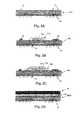
- FIGS. 1A-1Hare pictorial diagrams depicting stages in preparation of a semiconductor package in accordance with an embodiment of the present invention
- FIGS. 2A-2Care pictorial diagrams depicting further stages in assembly of a semiconductor package in accordance with another embodiment of the present invention.
- FIG. 2Dis a pictorial diagram depicting a semiconductor package in accordance with another embodiment of the present invention.
- FIG. 3Ais a pictorial diagram depicting a semiconductor package in accordance with another embodiment of the present invention.
- FIGS. 3B-3Care pictorial diagrams depicting stages in fabrication of a semiconductor package in accordance with yet another embodiment of the present invention.
- the present inventionconcerns a semiconductor package and a method for manufacturing a semiconductor package that include a metal layer formed atop a semiconductor package encapsulation and connected to an internal substrate of the semiconductor package by blind vias and/or terminals on the bottom side of the encapsulation by through vias.
- exemplary embodimentsdepict ball grid array packages, it will be understood by those skilled in the art, that the techniques of the present invention can be extended to other types of semiconductor packages.
- the exemplary embodimentsalso show wirebond die connections within the semiconductor package, but it will be understood that any type of internal die and die mounting can be used within the semiconductor package embodiments of the present invention.
- semiconductor package 10 Afor forming a semiconductor package in accordance with an embodiment of the invention and corresponding to a first illustrated step of manufacture is depicted.
- Semiconductor package 10 Ais in the form of a ball grid array (BGA) or land grid array (LGA) package as is commonly known in the art, except that particular circuit features are positioned for providing vias to the top side of semiconductor package 10 A in subsequent manufacturing steps, so that connections may be made to features to be formed in subsequent steps.
- BGAball grid array
- LGAland grid array
- Semiconductor package 10 Aincludes a die 16 mounted to a substrate 14 A that includes lands 18 to which solder ball terminals may be attached or that may be connected with a conductive paste to form a LGA mounted semiconductor package.
- Encapsulation 12 Asurrounds die 16 and substrate 14 A, although substrate 14 A may alternatively be exposed on a bottom side of semiconductor package 10 A.
- Electrical connections 15 of die 16are connected to circuit patterns 17 on substrate 14 A via wires 19 , but the type of die mounting is not limiting, but exemplary and other die mounting types may be used such as flip-chip die mounting.
- substrate 14 Ais depicted as a film or laminate-type mounting structure, lead frame and other substrate technologies may be used within the structures of the present invention.
- semiconductor package 10 Bincludes a plurality of via holes 20 A, 20 B and 20 C laser-ablated through encapsulation 12 A of FIG. 1A to form encapsulation 12 B. While only three via holes are shown, many via holes may be provided. The three via holes shown and as disclosed in the above-incorporated parent U.S. Patent Application illustrate the three different types of via holes that may be provided through control of laser energy and exposure time.
- the first via hole typeillustrated as via 20 A, is fabricated by laser-ablating either completely through semiconductor package 10 B or by laser-ablating through encapsulation 12 A to the top side of lands 18 , so that a connection is provided through from the top side of semiconductor package 10 B to the bottom side of semiconductor package 10 B when the via is filled. If via 20 A is ablated completely through, then the corresponding land 18 is provided by the bottom surface of a via formed in hole 20 A.
- the next type of via holeis provided by laser-ablating through encapsulation 12 A to reach circuit pattern 17 so that connection may be made through substrate 14 A circuit patterns to die 16 electrical terminals, to lands 18 or both.
- the last type of viais provided by laser-ablating through encapsulation 12 A to reach electrical connections 15 of die 16 so that direct connection to the circuits of die 16 can be made from a piggybacked semiconductor package.
- Each of via holes 20 A, 20 B and 20 Cis depicted as a via hole having a conical cross-section, which is desirable for providing uniform plating current density during a plating process.
- via holes 20 A, 20 B and 20 Cmay alternatively be made cylindrical in shape if the advantage of conical cross-section is not needed, for example if a conductive paste is used to fill the via holes.
- the conductive material used form vias 22 A, 22 B and 22 Cmay be electroplated or electro-less plated metal, conductive paste such as copper or silver epoxy compounds, or a low melting temperature high-wicking solder alloy such as SUPER SOLDER.
- Channels 24are laser-ablated in the top surface of encapsulation 12 C to form encapsulation 12 D.
- Channels 24may define circuit traces, terminals and other features that either provide complete interconnection at the top surface of encapsulation 12 D or connect top-side features such as circuit traces and terminals to one or more of vias 22 A, 22 B and 22 C.
- channels 24are filled to provide a metal layer 26 in a semiconductor package step 10 E.
- Channels 24may be filled by electroplating, filling with conductive paste with planarization if required, or electro-less plating after treating channels 24 with an activating compound.
- the top surface of encapsulation 12 Dmay be overplated or over-pasted and then etched to isolate the circuit features of metal layer 26 .
- plating 28may be applied as shown in FIG. 1F , yielding semiconductor package step 10 F to protect the surface of metal layer and/or to prepare terminal areas defined by the top surface of metal layer 26 for further processing such as wire bond attach or soldering.
- solder mask 30may be applied over the top of encapsulation 12 D and portions of the metal layer 26 , yielding semiconductor package step 10 G. Solder mask 30 is useful in operations where reflow solder operations will be used to attach components to metal layer 26 .
- Solder balls 34may be attached to bottom-side terminals 18 of semiconductor package step 10 G to yield a completed ball-grid-array (BGA) package 10 H that is ready for mounting on a circuit board or other mounting location.
- BGAball-grid-array
- the step illustrated in FIG. 1Hmay be omitted and bottom side terminals 18 plated, yielding a land-grid-array (LGA) package.
- a “tinning” coat of solder 32may be applied to the top side of semiconductor package 10 H as illustrated by FIG. 2A to prepare for mounting of top side components.
- the soldermay be selectively applied to only solder mounting terminal areas via a mask.
- FIG. 2Billustrates mounting of another semiconductor die 16 A that is wire-bonded via wires 19 A to plated terminals of metal layer 26 and also mounting of discrete surface-mount components 36 via reflow soldering.
- a second encapsulation 12 Emay be applied over die 16 A, wires 19 A and part of the top surface of encapsulation 12 D to form a completed assembly as illustrated in FIG. 2C .
- FIG. 2DAnother alternative embodiment of the present invention is shown in FIG. 2D .
- another semiconductor package 38may be ball-mounted to terminals formed on metal layer 26 .
- the depicted embodimentprovides for redistribution of terminals at virtually any position atop semiconductor package 10 H 2 , since metal layer 26 can provide routing of circuits from vias such as 22 A-C to solder balls 34 A at virtually any position atop semiconductor package 10 H 2 .
- FIG. 3Aillustrates another embodiment of the present invention that includes a metal layer 40 that provides a shield cap for semiconductor package 10 I.
- Metal layer 40may be electro-less plated atop encapsulation 12 C (See FIGS. 1A-1C for formation steps prior to FIG. 3A ) by applying a seed layer or may be paste screened to form metal layer 40 .
- Metal layermay be solid layer, or a continuous pattern such as a mesh screen to reduce separation and required metal to improve the plating process.
- Metal layer 40is electrically connected to vias 22 A and/or 22 B to provide a return path for the shield.
- FIG. 3Billustrates another shield embodiment of the present invention.
- a shield cavityis laser-ablated in the top surface of encapsulation 12 E to form a semiconductor package step 10 J having a cavity 24 A.
- Cavity 24 Ais then filled to form a metal shield layer 40 A as shown in FIG. 3C .
- Metal layer 40 Amay be applied by paste screening or plating (and possible subsequent etching process) to yield a shield that is contained within the sides of semiconductor package 10 K.
Landscapes
- Engineering & Computer Science (AREA)
- Microelectronics & Electronic Packaging (AREA)
- Power Engineering (AREA)
- Computer Hardware Design (AREA)
- Physics & Mathematics (AREA)
- General Physics & Mathematics (AREA)
- Condensed Matter Physics & Semiconductors (AREA)
- Ceramic Engineering (AREA)
- Manufacturing & Machinery (AREA)
- Health & Medical Sciences (AREA)
- Electromagnetism (AREA)
- Toxicology (AREA)
- Shielding Devices Or Components To Electric Or Magnetic Fields (AREA)
- Printing Elements For Providing Electric Connections Between Printed Circuits (AREA)
Abstract
Description
Claims (20)
Priority Applications (1)
| Application Number | Priority Date | Filing Date | Title |
|---|---|---|---|
| US13/136,457US8227338B1 (en) | 2004-03-23 | 2011-08-01 | Semiconductor package including a top-surface metal layer for implementing circuit features |
Applications Claiming Priority (4)
| Application Number | Priority Date | Filing Date | Title |
|---|---|---|---|
| US10/806,640US7185426B1 (en) | 2002-05-01 | 2004-03-23 | Method of manufacturing a semiconductor package |
| US11/293,999US7633765B1 (en) | 2004-03-23 | 2005-12-05 | Semiconductor package including a top-surface metal layer for implementing circuit features |
| US12/589,839US8018068B1 (en) | 2004-03-23 | 2009-10-28 | Semiconductor package including a top-surface metal layer for implementing circuit features |
| US13/136,457US8227338B1 (en) | 2004-03-23 | 2011-08-01 | Semiconductor package including a top-surface metal layer for implementing circuit features |
Related Parent Applications (1)
| Application Number | Title | Priority Date | Filing Date |
|---|---|---|---|
| US12/589,839ContinuationUS8018068B1 (en) | 2004-03-23 | 2009-10-28 | Semiconductor package including a top-surface metal layer for implementing circuit features |
Publications (1)
| Publication Number | Publication Date |
|---|---|
| US8227338B1true US8227338B1 (en) | 2012-07-24 |
Family
ID=41403300
Family Applications (3)
| Application Number | Title | Priority Date | Filing Date |
|---|---|---|---|
| US11/293,999Expired - LifetimeUS7633765B1 (en) | 2002-05-01 | 2005-12-05 | Semiconductor package including a top-surface metal layer for implementing circuit features |
| US12/589,839Expired - LifetimeUS8018068B1 (en) | 2004-03-23 | 2009-10-28 | Semiconductor package including a top-surface metal layer for implementing circuit features |
| US13/136,457Expired - LifetimeUS8227338B1 (en) | 2004-03-23 | 2011-08-01 | Semiconductor package including a top-surface metal layer for implementing circuit features |
Family Applications Before (2)
| Application Number | Title | Priority Date | Filing Date |
|---|---|---|---|
| US11/293,999Expired - LifetimeUS7633765B1 (en) | 2002-05-01 | 2005-12-05 | Semiconductor package including a top-surface metal layer for implementing circuit features |
| US12/589,839Expired - LifetimeUS8018068B1 (en) | 2004-03-23 | 2009-10-28 | Semiconductor package including a top-surface metal layer for implementing circuit features |
Country Status (1)
| Country | Link |
|---|---|
| US (3) | US7633765B1 (en) |
Cited By (19)
| Publication number | Priority date | Publication date | Assignee | Title |
|---|---|---|---|---|
| US20130032952A1 (en)* | 2011-08-01 | 2013-02-07 | Stats Chippac, Ltd. | Semiconductor Device and Method of Forming POP With Stacked Semiconductor Die and Bumps Formed Directly on the Lower Die |
| US20130049182A1 (en)* | 2011-08-31 | 2013-02-28 | Zhiwei Gong | Semiconductor device packaging having pre-encapsulation through via formation using lead frames with attached signal conduits |
| US20130105972A1 (en)* | 2011-11-01 | 2013-05-02 | Flextronics Ap, Llc | Stacked packages using laser direct structuring |
| US20130223041A1 (en)* | 2012-02-23 | 2013-08-29 | Apple Inc. | Low profile, space efficient circuit shields |
| US8597983B2 (en) | 2011-11-18 | 2013-12-03 | Freescale Semiconductor, Inc. | Semiconductor device packaging having substrate with pre-encapsulation through via formation |
| US20150130054A1 (en)* | 2013-11-13 | 2015-05-14 | Amkor Technology, Inc. | Semiconductor package structure and manufacturing method thereof |
| US9142502B2 (en) | 2011-08-31 | 2015-09-22 | Zhiwei Gong | Semiconductor device packaging having pre-encapsulation through via formation using drop-in signal conduits |
| US9691635B1 (en) | 2002-05-01 | 2017-06-27 | Amkor Technology, Inc. | Buildup dielectric layer having metallization pattern semiconductor package fabrication method |
| US9704747B2 (en) | 2013-03-29 | 2017-07-11 | Amkor Technology, Inc. | Semiconductor device and manufacturing method thereof |
| US9768140B2 (en)* | 2014-08-15 | 2017-09-19 | Siliconware Precision Industries Co., Ltd. | Method for fabricating package structure |
| US9812386B1 (en) | 2002-05-01 | 2017-11-07 | Amkor Technology, Inc. | Encapsulated semiconductor package |
| US9842799B2 (en) | 2014-10-27 | 2017-12-12 | Samsung Electronics Co., Ltd. | Semiconductor packages including upper and lower packages and heat dissipation parts |
| US9953931B1 (en) | 2016-10-25 | 2018-04-24 | Advanced Semiconductor Engineering, Inc | Semiconductor device package and a method of manufacturing the same |
| CN108370109A (en)* | 2015-09-01 | 2018-08-03 | R&D电路股份有限公司 | Interconnects with traces anywhere |
| CN110556402A (en)* | 2018-06-01 | 2019-12-10 | 群创光电股份有限公司 | Electronic device |
| US10573573B2 (en)* | 2018-03-20 | 2020-02-25 | Taiwan Semiconductor Manufacturing Co., Ltd. | Package and package-on-package structure having elliptical conductive columns |
| US10672738B2 (en)* | 2014-09-05 | 2020-06-02 | Taiwan Semiconductor Manufacturing Company, Ltd. | Package structures and methods of forming |
| US10811277B2 (en) | 2004-03-23 | 2020-10-20 | Amkor Technology, Inc. | Encapsulated semiconductor package |
| US11081370B2 (en) | 2004-03-23 | 2021-08-03 | Amkor Technology Singapore Holding Pte. Ltd. | Methods of manufacturing an encapsulated semiconductor device |
Families Citing this family (206)
| Publication number | Priority date | Publication date | Assignee | Title |
|---|---|---|---|---|
| US6930256B1 (en) | 2002-05-01 | 2005-08-16 | Amkor Technology, Inc. | Integrated circuit substrate having laser-embedded conductive patterns and method therefor |
| US7633765B1 (en) | 2004-03-23 | 2009-12-15 | Amkor Technology, Inc. | Semiconductor package including a top-surface metal layer for implementing circuit features |
| KR101313391B1 (en) | 2004-11-03 | 2013-10-01 | 테세라, 인코포레이티드 | Stacked packaging improvements |
| US20090002969A1 (en) | 2007-06-27 | 2009-01-01 | Rf Micro Devices, Inc. | Field barrier structures within a conformal shield |
| US8959762B2 (en) | 2005-08-08 | 2015-02-24 | Rf Micro Devices, Inc. | Method of manufacturing an electronic module |
| US8058101B2 (en) | 2005-12-23 | 2011-11-15 | Tessera, Inc. | Microelectronic packages and methods therefor |
| US7993972B2 (en) | 2008-03-04 | 2011-08-09 | Stats Chippac, Ltd. | Wafer level die integration and method therefor |
| US8546929B2 (en)* | 2006-04-19 | 2013-10-01 | Stats Chippac Ltd. | Embedded integrated circuit package-on-package system |
| US8174119B2 (en)* | 2006-11-10 | 2012-05-08 | Stats Chippac, Ltd. | Semiconductor package with embedded die |
| US7550857B1 (en) | 2006-11-16 | 2009-06-23 | Amkor Technology, Inc. | Stacked redistribution layer (RDL) die assembly package |
| US9466545B1 (en) | 2007-02-21 | 2016-10-11 | Amkor Technology, Inc. | Semiconductor package in package |
| TWI335070B (en) | 2007-03-23 | 2010-12-21 | Advanced Semiconductor Eng | Semiconductor package and the method of making the same |
| US8440916B2 (en)* | 2007-06-28 | 2013-05-14 | Intel Corporation | Method of forming a substrate core structure using microvia laser drilling and conductive layer pre-patterning and substrate core structure formed according to the method |
| TWI349974B (en)* | 2007-07-06 | 2011-10-01 | Unimicron Technology Corp | Structure with embedded circuit |
| KR101572600B1 (en) | 2007-10-10 | 2015-11-27 | 테세라, 인코포레이티드 | Robust multi-layer wiring elements and assemblies with embedded microelectronic elements |
| JP5081578B2 (en)* | 2007-10-25 | 2012-11-28 | ローム株式会社 | Resin-sealed semiconductor device |
| US8350367B2 (en) | 2008-02-05 | 2013-01-08 | Advanced Semiconductor Engineering, Inc. | Semiconductor device packages with electromagnetic interference shielding |
| US7989928B2 (en) | 2008-02-05 | 2011-08-02 | Advanced Semiconductor Engineering Inc. | Semiconductor device packages with electromagnetic interference shielding |
| US8212339B2 (en) | 2008-02-05 | 2012-07-03 | Advanced Semiconductor Engineering, Inc. | Semiconductor device packages with electromagnetic interference shielding |
| US8022511B2 (en) | 2008-02-05 | 2011-09-20 | Advanced Semiconductor Engineering, Inc. | Semiconductor device packages with electromagnetic interference shielding |
| JPWO2009144960A1 (en)* | 2008-05-30 | 2011-10-06 | 三洋電機株式会社 | Semiconductor module, semiconductor module manufacturing method, and portable device |
| TWI473553B (en) | 2008-07-03 | 2015-02-11 | Advanced Semiconductor Eng | Chip package structure |
| TWI453877B (en)* | 2008-11-07 | 2014-09-21 | Advanced Semiconductor Eng | Structure and process of embedded chip package |
| US8270176B2 (en)* | 2008-08-08 | 2012-09-18 | Stats Chippac Ltd. | Exposed interconnect for a package on package system |
| US8410584B2 (en) | 2008-08-08 | 2013-04-02 | Advanced Semiconductor Engineering, Inc. | Semiconductor device packages with electromagnetic interference shielding |
| US20100110656A1 (en) | 2008-10-31 | 2010-05-06 | Advanced Semiconductor Engineering, Inc. | Chip package and manufacturing method thereof |
| US20100207257A1 (en)* | 2009-02-17 | 2010-08-19 | Advanced Semiconductor Engineering, Inc. | Semiconductor package and manufacturing method thereof |
| US8110902B2 (en) | 2009-02-19 | 2012-02-07 | Advanced Semiconductor Engineering, Inc. | Chip package and manufacturing method thereof |
| US8710634B2 (en)* | 2009-03-25 | 2014-04-29 | Stats Chippac Ltd. | Integrated circuit packaging system with an integral-interposer-structure and method of manufacture thereof |
| US20100244223A1 (en)* | 2009-03-25 | 2010-09-30 | Cho Namju | Integrated circuit packaging system with an integral-interposer-structure and method of manufacture thereof |
| US9355962B2 (en)* | 2009-06-12 | 2016-05-31 | Stats Chippac Ltd. | Integrated circuit package stacking system with redistribution and method of manufacture thereof |
| US8222538B1 (en) | 2009-06-12 | 2012-07-17 | Amkor Technology, Inc. | Stackable via package and method |
| US8212340B2 (en) | 2009-07-13 | 2012-07-03 | Advanced Semiconductor Engineering, Inc. | Chip package and manufacturing method thereof |
| US8310835B2 (en)* | 2009-07-14 | 2012-11-13 | Apple Inc. | Systems and methods for providing vias through a modular component |
| US8471154B1 (en) | 2009-08-06 | 2013-06-25 | Amkor Technology, Inc. | Stackable variable height via package and method |
| US8432022B1 (en)* | 2009-09-29 | 2013-04-30 | Amkor Technology, Inc. | Shielded embedded electronic component substrate fabrication method and structure |
| US8198131B2 (en) | 2009-11-18 | 2012-06-12 | Advanced Semiconductor Engineering, Inc. | Stackable semiconductor device packages |
| US8030750B2 (en) | 2009-11-19 | 2011-10-04 | Advanced Semiconductor Engineering, Inc. | Semiconductor device packages with electromagnetic interference shielding |
| US8378466B2 (en) | 2009-11-19 | 2013-02-19 | Advanced Semiconductor Engineering, Inc. | Wafer-level semiconductor device packages with electromagnetic interference shielding |
| US8368185B2 (en) | 2009-11-19 | 2013-02-05 | Advanced Semiconductor Engineering, Inc. | Semiconductor device packages with electromagnetic interference shielding |
| US8327532B2 (en)* | 2009-11-23 | 2012-12-11 | Freescale Semiconductor, Inc. | Method for releasing a microelectronic assembly from a carrier substrate |
| US8937381B1 (en) | 2009-12-03 | 2015-01-20 | Amkor Technology, Inc. | Thin stackable package and method |
| US9691734B1 (en) | 2009-12-07 | 2017-06-27 | Amkor Technology, Inc. | Method of forming a plurality of electronic component packages |
| US8304286B2 (en)* | 2009-12-11 | 2012-11-06 | Stats Chippac Ltd. | Integrated circuit packaging system with shielded package and method of manufacture thereof |
| TWI408785B (en) | 2009-12-31 | 2013-09-11 | Advanced Semiconductor Eng | Semiconductor package |
| US8569894B2 (en) | 2010-01-13 | 2013-10-29 | Advanced Semiconductor Engineering, Inc. | Semiconductor package with single sided substrate design and manufacturing methods thereof |
| US8320134B2 (en) | 2010-02-05 | 2012-11-27 | Advanced Semiconductor Engineering, Inc. | Embedded component substrate and manufacturing methods thereof |
| JP5503322B2 (en)* | 2010-02-15 | 2014-05-28 | ルネサスエレクトロニクス株式会社 | Manufacturing method of semiconductor device |
| TWI419283B (en) | 2010-02-10 | 2013-12-11 | Advanced Semiconductor Eng | Package structure |
| US8199518B1 (en) | 2010-02-18 | 2012-06-12 | Amkor Technology, Inc. | Top feature package and method |
| TWI411075B (en) | 2010-03-22 | 2013-10-01 | Advanced Semiconductor Eng | Semiconductor package and manufacturing method thereof |
| US8643181B2 (en)* | 2010-03-24 | 2014-02-04 | Stats Chippac Ltd. | Integrated circuit packaging system with encapsulation and method of manufacture thereof |
| US8278746B2 (en) | 2010-04-02 | 2012-10-02 | Advanced Semiconductor Engineering, Inc. | Semiconductor device packages including connecting elements |
| US8624374B2 (en) | 2010-04-02 | 2014-01-07 | Advanced Semiconductor Engineering, Inc. | Semiconductor device packages with fan-out and with connecting elements for stacking and manufacturing methods thereof |
| US8946886B1 (en) | 2010-05-13 | 2015-02-03 | Amkor Technology, Inc. | Shielded electronic component package and method |
| US8558392B2 (en) | 2010-05-14 | 2013-10-15 | Stats Chippac, Ltd. | Semiconductor device and method of forming interconnect structure and mounting semiconductor die in recessed encapsulant |
| US8300423B1 (en) | 2010-05-25 | 2012-10-30 | Amkor Technology, Inc. | Stackable treated via package and method |
| US8294276B1 (en) | 2010-05-27 | 2012-10-23 | Amkor Technology, Inc. | Semiconductor device and fabricating method thereof |
| US9159708B2 (en) | 2010-07-19 | 2015-10-13 | Tessera, Inc. | Stackable molded microelectronic packages with area array unit connectors |
| US8482111B2 (en) | 2010-07-19 | 2013-07-09 | Tessera, Inc. | Stackable molded microelectronic packages |
| KR101119348B1 (en)* | 2010-07-23 | 2012-03-07 | 삼성전기주식회사 | Semiconductor module and manufactureing method thereof |
| US8338229B1 (en) | 2010-07-30 | 2012-12-25 | Amkor Technology, Inc. | Stackable plasma cleaned via package and method |
| TWI540698B (en) | 2010-08-02 | 2016-07-01 | 日月光半導體製造股份有限公司 | Semiconductor package and manufacturing method thereof |
| US8717775B1 (en) | 2010-08-02 | 2014-05-06 | Amkor Technology, Inc. | Fingerprint sensor package and method |
| US8895440B2 (en)* | 2010-08-06 | 2014-11-25 | Stats Chippac, Ltd. | Semiconductor die and method of forming Fo-WLCSP vertical interconnect using TSV and TMV |
| US8343810B2 (en)* | 2010-08-16 | 2013-01-01 | Stats Chippac, Ltd. | Semiconductor device and method of forming Fo-WLCSP having conductive layers and conductive vias separated by polymer layers |
| US9137934B2 (en) | 2010-08-18 | 2015-09-15 | Rf Micro Devices, Inc. | Compartmentalized shielding of selected components |
| TWI460834B (en)* | 2010-08-26 | 2014-11-11 | Unimicron Technology Corp | Package structure having (tsv) through-silicon-vias chip embedded therein and fabrication method thereof |
| US9007273B2 (en) | 2010-09-09 | 2015-04-14 | Advances Semiconductor Engineering, Inc. | Semiconductor package integrated with conformal shield and antenna |
| US8337657B1 (en) | 2010-10-27 | 2012-12-25 | Amkor Technology, Inc. | Mechanical tape separation package and method |
| TWI451546B (en) | 2010-10-29 | 2014-09-01 | Advanced Semiconductor Eng | Stacked semiconductor package, semiconductor package thereof and method for making a semiconductor package |
| US8482134B1 (en) | 2010-11-01 | 2013-07-09 | Amkor Technology, Inc. | Stackable package and method |
| US9748154B1 (en) | 2010-11-04 | 2017-08-29 | Amkor Technology, Inc. | Wafer level fan out semiconductor device and manufacturing method thereof |
| US8525318B1 (en) | 2010-11-10 | 2013-09-03 | Amkor Technology, Inc. | Semiconductor device and fabricating method thereof |
| KR101075241B1 (en) | 2010-11-15 | 2011-11-01 | 테세라, 인코포레이티드 | Microelectronic package with terminals in dielectric member |
| TWI538071B (en)* | 2010-11-16 | 2016-06-11 | 星科金朋有限公司 | Integrated circuit packaging system with connection structure and method of manufacture thereof |
| US8557629B1 (en) | 2010-12-03 | 2013-10-15 | Amkor Technology, Inc. | Semiconductor device having overlapped via apertures |
| US8310040B2 (en)* | 2010-12-08 | 2012-11-13 | General Electric Company | Semiconductor device package having high breakdown voltage and low parasitic inductance and method of manufacturing thereof |
| US8535961B1 (en) | 2010-12-09 | 2013-09-17 | Amkor Technology, Inc. | Light emitting diode (LED) package and method |
| US20120146206A1 (en) | 2010-12-13 | 2012-06-14 | Tessera Research Llc | Pin attachment |
| US9406658B2 (en)* | 2010-12-17 | 2016-08-02 | Advanced Semiconductor Engineering, Inc. | Embedded component device and manufacturing methods thereof |
| US9059160B1 (en)* | 2010-12-23 | 2015-06-16 | Marvell International Ltd. | Semiconductor package assembly |
| US9721872B1 (en) | 2011-02-18 | 2017-08-01 | Amkor Technology, Inc. | Methods and structures for increasing the allowable die size in TMV packages |
| US8835226B2 (en) | 2011-02-25 | 2014-09-16 | Rf Micro Devices, Inc. | Connection using conductive vias |
| US9171792B2 (en) | 2011-02-28 | 2015-10-27 | Advanced Semiconductor Engineering, Inc. | Semiconductor device packages having a side-by-side device arrangement and stacking functionality |
| US9627230B2 (en) | 2011-02-28 | 2017-04-18 | Qorvo Us, Inc. | Methods of forming a microshield on standard QFN package |
| US9013011B1 (en) | 2011-03-11 | 2015-04-21 | Amkor Technology, Inc. | Stacked and staggered die MEMS package and method |
| US8487426B2 (en) | 2011-03-15 | 2013-07-16 | Advanced Semiconductor Engineering, Inc. | Semiconductor package with embedded die and manufacturing methods thereof |
| KR101140113B1 (en) | 2011-04-26 | 2012-04-30 | 앰코 테크놀로지 코리아 주식회사 | Semiconductor device |
| KR101128063B1 (en) | 2011-05-03 | 2012-04-23 | 테세라, 인코포레이티드 | Package-on-package assembly with wire bonds to encapsulation surface |
| US8618659B2 (en) | 2011-05-03 | 2013-12-31 | Tessera, Inc. | Package-on-package assembly with wire bonds to encapsulation surface |
| US8872318B2 (en) | 2011-08-24 | 2014-10-28 | Tessera, Inc. | Through interposer wire bond using low CTE interposer with coarse slot apertures |
| US8653674B1 (en) | 2011-09-15 | 2014-02-18 | Amkor Technology, Inc. | Electronic component package fabrication method and structure |
| US8633598B1 (en) | 2011-09-20 | 2014-01-21 | Amkor Technology, Inc. | Underfill contacting stacking balls package fabrication method and structure |
| US9385009B2 (en) | 2011-09-23 | 2016-07-05 | STATS ChipPAC Pte. Ltd. | Semiconductor device and method of forming stacked vias within interconnect structure for Fo-WLCSP |
| US8872312B2 (en)* | 2011-09-30 | 2014-10-28 | Taiwan Semiconductor Manufacturing Company, Ltd. | EMI package and method for making same |
| US9029962B1 (en) | 2011-10-12 | 2015-05-12 | Amkor Technology, Inc. | Molded cavity substrate MEMS package fabrication method and structure |
| US8836136B2 (en) | 2011-10-17 | 2014-09-16 | Invensas Corporation | Package-on-package assembly with wire bond vias |
| US8541883B2 (en) | 2011-11-29 | 2013-09-24 | Advanced Semiconductor Engineering, Inc. | Semiconductor device having shielded conductive vias |
| US20130154106A1 (en)* | 2011-12-14 | 2013-06-20 | Broadcom Corporation | Stacked Packaging Using Reconstituted Wafers |
| US8946757B2 (en) | 2012-02-17 | 2015-02-03 | Invensas Corporation | Heat spreading substrate with embedded interconnects |
| US9349706B2 (en) | 2012-02-24 | 2016-05-24 | Invensas Corporation | Method for package-on-package assembly with wire bonds to encapsulation surface |
| US8372741B1 (en) | 2012-02-24 | 2013-02-12 | Invensas Corporation | Method for package-on-package assembly with wire bonds to encapsulation surface |
| TWI508249B (en) | 2012-04-02 | 2015-11-11 | 矽品精密工業股份有限公司 | Package structure, semiconductor package and fabrication method thereof |
| US8937376B2 (en) | 2012-04-16 | 2015-01-20 | Advanced Semiconductor Engineering, Inc. | Semiconductor packages with heat dissipation structures and related methods |
| US8901730B2 (en) | 2012-05-03 | 2014-12-02 | Taiwan Semiconductor Manufacturing Company, Ltd. | Methods and apparatus for package on package devices |
| US8786060B2 (en) | 2012-05-04 | 2014-07-22 | Advanced Semiconductor Engineering, Inc. | Semiconductor package integrated with conformal shield and antenna |
| US8704341B2 (en) | 2012-05-15 | 2014-04-22 | Advanced Semiconductor Engineering, Inc. | Semiconductor packages with thermal dissipation structures and EMI shielding |
| US8835228B2 (en) | 2012-05-22 | 2014-09-16 | Invensas Corporation | Substrate-less stackable package with wire-bond interconnect |
| US8653634B2 (en) | 2012-06-11 | 2014-02-18 | Advanced Semiconductor Engineering, Inc. | EMI-shielded semiconductor devices and methods of making |
| US9391008B2 (en) | 2012-07-31 | 2016-07-12 | Invensas Corporation | Reconstituted wafer-level package DRAM |
| US9153542B2 (en) | 2012-08-01 | 2015-10-06 | Advanced Semiconductor Engineering, Inc. | Semiconductor package having an antenna and manufacturing method thereof |
| US9502390B2 (en) | 2012-08-03 | 2016-11-22 | Invensas Corporation | BVA interposer |
| US8987851B2 (en) | 2012-09-07 | 2015-03-24 | Mediatek Inc. | Radio-frequency device package and method for fabricating the same |
| US9331007B2 (en) | 2012-10-16 | 2016-05-03 | Stats Chippac, Ltd. | Semiconductor device and method of forming conductive ink layer as interconnect structure between semiconductor packages |
| KR101419597B1 (en)* | 2012-11-06 | 2014-07-14 | 앰코 테크놀로지 코리아 주식회사 | Semiconductor device and manufacturing method thereof |
| US8975738B2 (en) | 2012-11-12 | 2015-03-10 | Invensas Corporation | Structure for microelectronic packaging with terminals on dielectric mass |
| US9799592B2 (en) | 2013-11-19 | 2017-10-24 | Amkor Technology, Inc. | Semicondutor device with through-silicon via-less deep wells |
| KR101366461B1 (en) | 2012-11-20 | 2014-02-26 | 앰코 테크놀로지 코리아 주식회사 | Semiconductor device and manufacturing method thereof |
| US9406552B2 (en) | 2012-12-20 | 2016-08-02 | Advanced Semiconductor Engineering, Inc. | Semiconductor device having conductive via and manufacturing process |
| US8878353B2 (en) | 2012-12-20 | 2014-11-04 | Invensas Corporation | Structure for microelectronic packaging with bond elements to encapsulation surface |
| US9136254B2 (en) | 2013-02-01 | 2015-09-15 | Invensas Corporation | Microelectronic package having wire bond vias and stiffening layer |
| US9978688B2 (en) | 2013-02-28 | 2018-05-22 | Advanced Semiconductor Engineering, Inc. | Semiconductor package having a waveguide antenna and manufacturing method thereof |
| US9837701B2 (en) | 2013-03-04 | 2017-12-05 | Advanced Semiconductor Engineering, Inc. | Semiconductor package including antenna substrate and manufacturing method thereof |
| US9129954B2 (en) | 2013-03-07 | 2015-09-08 | Advanced Semiconductor Engineering, Inc. | Semiconductor package including antenna layer and manufacturing method thereof |
| US9172131B2 (en) | 2013-03-15 | 2015-10-27 | Advanced Semiconductor Engineering, Inc. | Semiconductor structure having aperture antenna |
| US9807890B2 (en) | 2013-05-31 | 2017-10-31 | Qorvo Us, Inc. | Electronic modules having grounded electromagnetic shields |
| US9023691B2 (en) | 2013-07-15 | 2015-05-05 | Invensas Corporation | Microelectronic assemblies with stack terminals coupled by connectors extending through encapsulation |
| US9034696B2 (en) | 2013-07-15 | 2015-05-19 | Invensas Corporation | Microelectronic assemblies having reinforcing collars on connectors extending through encapsulation |
| US8883563B1 (en) | 2013-07-15 | 2014-11-11 | Invensas Corporation | Fabrication of microelectronic assemblies having stack terminals coupled by connectors extending through encapsulation |
| CN103400825B (en) | 2013-07-31 | 2016-05-18 | 日月光半导体制造股份有限公司 | Semiconductor package and manufacturing method thereof |
| US9167710B2 (en) | 2013-08-07 | 2015-10-20 | Invensas Corporation | Embedded packaging with preformed vias |
| US9685365B2 (en) | 2013-08-08 | 2017-06-20 | Invensas Corporation | Method of forming a wire bond having a free end |
| US9801277B1 (en)* | 2013-08-27 | 2017-10-24 | Flextronics Ap, Llc | Bellows interconnect |
| US9237647B2 (en)* | 2013-09-12 | 2016-01-12 | Taiwan Semiconductor Manufacturing Company, Ltd. | Package-on-package structure with through molding via |
| US20150076714A1 (en) | 2013-09-16 | 2015-03-19 | Invensas Corporation | Microelectronic element with bond elements to encapsulation surface |
| KR101607981B1 (en) | 2013-11-04 | 2016-03-31 | 앰코 테크놀로지 코리아 주식회사 | Interposer and method for manufacturing the same, and semiconductor package using the same |
| US9082753B2 (en) | 2013-11-12 | 2015-07-14 | Invensas Corporation | Severing bond wire by kinking and twisting |
| US9087815B2 (en) | 2013-11-12 | 2015-07-21 | Invensas Corporation | Off substrate kinking of bond wire |
| US9379074B2 (en) | 2013-11-22 | 2016-06-28 | Invensas Corporation | Die stacks with one or more bond via arrays of wire bond wires and with one or more arrays of bump interconnects |
| US9583456B2 (en) | 2013-11-22 | 2017-02-28 | Invensas Corporation | Multiple bond via arrays of different wire heights on a same substrate |
| US9263394B2 (en) | 2013-11-22 | 2016-02-16 | Invensas Corporation | Multiple bond via arrays of different wire heights on a same substrate |
| JP6279754B2 (en)* | 2013-12-09 | 2018-02-14 | インテル コーポレイション | Antenna on ceramic for packaged dies |
| US9202742B1 (en) | 2014-01-15 | 2015-12-01 | Stats Chippac Ltd. | Integrated circuit packaging system with pattern-through-mold and method of manufacture thereof |
| US9583411B2 (en) | 2014-01-17 | 2017-02-28 | Invensas Corporation | Fine pitch BVA using reconstituted wafer with area array accessible for testing |
| US9894816B2 (en)* | 2014-02-04 | 2018-02-13 | Taiyo Yuden Co., Ltd. | Circuit module |
| US9355997B2 (en) | 2014-03-12 | 2016-05-31 | Invensas Corporation | Integrated circuit assemblies with reinforcement frames, and methods of manufacture |
| US20150262902A1 (en) | 2014-03-12 | 2015-09-17 | Invensas Corporation | Integrated circuits protected by substrates with cavities, and methods of manufacture |
| US9214454B2 (en) | 2014-03-31 | 2015-12-15 | Invensas Corporation | Batch process fabrication of package-on-package microelectronic assemblies |
| US9165793B1 (en) | 2014-05-02 | 2015-10-20 | Invensas Corporation | Making electrical components in handle wafers of integrated circuit packages |
| US9257396B2 (en)* | 2014-05-22 | 2016-02-09 | Invensas Corporation | Compact semiconductor package and related methods |
| US10381326B2 (en) | 2014-05-28 | 2019-08-13 | Invensas Corporation | Structure and method for integrated circuits packaging with increased density |
| US9646917B2 (en) | 2014-05-29 | 2017-05-09 | Invensas Corporation | Low CTE component with wire bond interconnects |
| US9412714B2 (en) | 2014-05-30 | 2016-08-09 | Invensas Corporation | Wire bond support structure and microelectronic package including wire bonds therefrom |
| US9741649B2 (en) | 2014-06-04 | 2017-08-22 | Invensas Corporation | Integrated interposer solutions for 2D and 3D IC packaging |
| US9252127B1 (en) | 2014-07-10 | 2016-02-02 | Invensas Corporation | Microelectronic assemblies with integrated circuits and interposers with cavities, and methods of manufacture |
| US9735084B2 (en) | 2014-12-11 | 2017-08-15 | Invensas Corporation | Bond via array for thermal conductivity |
| US9888579B2 (en) | 2015-03-05 | 2018-02-06 | Invensas Corporation | Pressing of wire bond wire tips to provide bent-over tips |
| CN104779220A (en)* | 2015-03-27 | 2015-07-15 | 矽力杰半导体技术(杭州)有限公司 | Chip packaging structure and manufacture method thereof |
| US9502372B1 (en) | 2015-04-30 | 2016-11-22 | Invensas Corporation | Wafer-level packaging using wire bond wires in place of a redistribution layer |
| US9761554B2 (en) | 2015-05-07 | 2017-09-12 | Invensas Corporation | Ball bonding metal wire bond wires to metal pads |
| US10685943B2 (en) | 2015-05-14 | 2020-06-16 | Mediatek Inc. | Semiconductor chip package with resilient conductive paste post and fabrication method thereof |
| US9842831B2 (en) | 2015-05-14 | 2017-12-12 | Mediatek Inc. | Semiconductor package and fabrication method thereof |
| US9478504B1 (en) | 2015-06-19 | 2016-10-25 | Invensas Corporation | Microelectronic assemblies with cavities, and methods of fabrication |
| US9490222B1 (en) | 2015-10-12 | 2016-11-08 | Invensas Corporation | Wire bond wires for interference shielding |
| US10490528B2 (en) | 2015-10-12 | 2019-11-26 | Invensas Corporation | Embedded wire bond wires |
| US10332854B2 (en) | 2015-10-23 | 2019-06-25 | Invensas Corporation | Anchoring structure of fine pitch bva |
| US10181457B2 (en) | 2015-10-26 | 2019-01-15 | Invensas Corporation | Microelectronic package for wafer-level chip scale packaging with fan-out |
| US10043779B2 (en) | 2015-11-17 | 2018-08-07 | Invensas Corporation | Packaged microelectronic device for a package-on-package device |
| US9659848B1 (en) | 2015-11-18 | 2017-05-23 | Invensas Corporation | Stiffened wires for offset BVA |
| US10449729B1 (en) | 2015-12-03 | 2019-10-22 | Multek Technologies Ltd. | 3D printed fiber optics |
| US9984992B2 (en) | 2015-12-30 | 2018-05-29 | Invensas Corporation | Embedded wire bond wires for vertical integration with separate surface mount and wire bond mounting surfaces |
| US10204883B2 (en)* | 2016-02-02 | 2019-02-12 | Taiwan Semidonductor Manufacturing Company Ltd. | Semiconductor device and manufacturing method thereof |
| JP6524003B2 (en)* | 2016-03-17 | 2019-06-05 | 東芝メモリ株式会社 | Semiconductor device |
| US9935075B2 (en) | 2016-07-29 | 2018-04-03 | Invensas Corporation | Wire bonding method and apparatus for electromagnetic interference shielding |
| US9960328B2 (en) | 2016-09-06 | 2018-05-01 | Amkor Technology, Inc. | Semiconductor device and manufacturing method thereof |
| US20180114786A1 (en) | 2016-10-21 | 2018-04-26 | Powertech Technology Inc. | Method of forming package-on-package structure |
| US10299368B2 (en) | 2016-12-21 | 2019-05-21 | Invensas Corporation | Surface integrated waveguides and circuit structures therefor |
| EP3346492A3 (en)* | 2017-01-05 | 2018-08-08 | MediaTek Inc. | Semiconductor chip package and fabrication method thereof |
| US10177095B2 (en) | 2017-03-24 | 2019-01-08 | Amkor Technology, Inc. | Semiconductor device and method of manufacturing thereof |
| CN210074170U (en)* | 2017-04-03 | 2020-02-14 | 株式会社村田制作所 | High frequency module |
| US11101224B2 (en)* | 2017-06-08 | 2021-08-24 | Futurewei Technologies, Inc. | Wrapped signal shielding in a wafer fanout package |
| US10741466B2 (en) | 2017-11-17 | 2020-08-11 | Infineon Technologies Ag | Formation of conductive connection tracks in package mold body using electroless plating |
| EP3495318A3 (en) | 2017-12-08 | 2019-08-21 | Infineon Technologies AG | Semiconductor package with air cavity |
| US20190214327A1 (en)* | 2018-01-10 | 2019-07-11 | Sonja Koller | Thermal conduction devices and methods for embedded electronic devices |
| KR102531817B1 (en)* | 2018-03-28 | 2023-05-12 | 한미반도체 주식회사 | Partial shield processing method for semiconductor member |
| US11735570B2 (en)* | 2018-04-04 | 2023-08-22 | Intel Corporation | Fan out packaging pop mechanical attach method |
| US11127689B2 (en) | 2018-06-01 | 2021-09-21 | Qorvo Us, Inc. | Segmented shielding using wirebonds |
| US11219144B2 (en) | 2018-06-28 | 2022-01-04 | Qorvo Us, Inc. | Electromagnetic shields for sub-modules |
| US11211340B2 (en) | 2018-11-28 | 2021-12-28 | Shiann-Tsong Tsai | Semiconductor package with in-package compartmental shielding and active electro-magnetic compatibility shielding |
| US10923435B2 (en)* | 2018-11-28 | 2021-02-16 | Shiann-Tsong Tsai | Semiconductor package with in-package compartmental shielding and improved heat-dissipation performance |
| US11239179B2 (en) | 2018-11-28 | 2022-02-01 | Shiann-Tsong Tsai | Semiconductor package and fabrication method thereof |
| US11114363B2 (en) | 2018-12-20 | 2021-09-07 | Qorvo Us, Inc. | Electronic package arrangements and related methods |
| US11133281B2 (en) | 2019-04-04 | 2021-09-28 | Infineon Technologies Ag | Chip to chip interconnect in encapsulant of molded semiconductor package |
| US10796981B1 (en) | 2019-04-04 | 2020-10-06 | Infineon Technologies Ag | Chip to lead interconnect in encapsulant of molded semiconductor package |
| US11515282B2 (en) | 2019-05-21 | 2022-11-29 | Qorvo Us, Inc. | Electromagnetic shields with bonding wires for sub-modules |
| CN112018052A (en) | 2019-05-31 | 2020-12-01 | 英飞凌科技奥地利有限公司 | Semiconductor package with laser activatable molding compound |
| WO2020250795A1 (en)* | 2019-06-10 | 2020-12-17 | 株式会社ライジングテクノロジーズ | Electronic circuit device |
| CN110190002B (en)* | 2019-07-04 | 2021-01-12 | 环维电子(上海)有限公司 | Semiconductor assembly and manufacturing method thereof |
| TWI719866B (en)* | 2020-03-25 | 2021-02-21 | 矽品精密工業股份有限公司 | Electronic package, supporting structure and manufacturing method thereof |
| US11587800B2 (en) | 2020-05-22 | 2023-02-21 | Infineon Technologies Ag | Semiconductor package with lead tip inspection feature |
| KR20220000087A (en)* | 2020-06-25 | 2022-01-03 | 삼성전기주식회사 | Electronic device module |
| TWI749860B (en)* | 2020-11-10 | 2021-12-11 | 菱生精密工業股份有限公司 | Chip packaging method |
| US11652065B2 (en)* | 2021-05-04 | 2023-05-16 | STATS ChipPAC Pte. Ltd. | Semiconductor device and method of embedding circuit pattern in encapsulant for SIP module |
| US11610847B2 (en) | 2021-05-07 | 2023-03-21 | STATS ChipPAC Pte. Ltd. | Laser-based redistribution and multi-stacked packages |
| US11749668B2 (en) | 2021-06-09 | 2023-09-05 | STATS ChipPAC Pte. Ltd | PSPI-based patterning method for RDL |
Citations (176)
| Publication number | Priority date | Publication date | Assignee | Title |
|---|---|---|---|---|
| US3868724A (en) | 1973-11-21 | 1975-02-25 | Fairchild Camera Instr Co | Multi-layer connecting structures for packaging semiconductor devices mounted on a flexible carrier |
| US3916434A (en) | 1972-11-30 | 1975-10-28 | Power Hybrids Inc | Hermetically sealed encapsulation of semiconductor devices |
| US4322778A (en) | 1980-01-25 | 1982-03-30 | International Business Machines Corp. | High performance semiconductor package assembly |
| US4532419A (en) | 1982-09-09 | 1985-07-30 | Sony Corporation | Memory card having static electricity protection |
| US4642160A (en) | 1985-08-12 | 1987-02-10 | Interconnect Technology Inc. | Multilayer circuit board manufacturing |
| US4645552A (en) | 1984-11-19 | 1987-02-24 | Hughes Aircraft Company | Process for fabricating dimensionally stable interconnect boards |
| US4685033A (en) | 1984-08-28 | 1987-08-04 | Nec Corporation | Multilayer wiring substrate |
| US4706167A (en) | 1983-11-10 | 1987-11-10 | Telemark Co., Inc. | Circuit wiring disposed on solder mask coating |
| US4716049A (en) | 1985-12-20 | 1987-12-29 | Hughes Aircraft Company | Compressive pedestal for microminiature connections |
| US4786952A (en) | 1986-07-24 | 1988-11-22 | General Motors Corporation | High voltage depletion mode MOS power field effect transistor |
| US4806188A (en) | 1988-03-04 | 1989-02-21 | E. I. Du Pont De Nemours And Company | Method for fabricating multilayer circuits |
| US4811082A (en) | 1986-11-12 | 1989-03-07 | International Business Machines Corporation | High performance integrated circuit packaging structure |
| US4897338A (en) | 1987-08-03 | 1990-01-30 | Allied-Signal Inc. | Method for the manufacture of multilayer printed circuit boards |
| US4905124A (en) | 1987-03-31 | 1990-02-27 | Mitsubishi Denki Kabushiki Kaisha | IC card |
| US4964212A (en) | 1988-09-29 | 1990-10-23 | Commissariat A L'energie Atomique | Process for producing electrical connections through a substrate |
| US4974120A (en) | 1989-01-12 | 1990-11-27 | Mitsubishi Denki Kabushiki Kaisha | IC card |
| US4996391A (en) | 1988-09-30 | 1991-02-26 | Siemens Aktiengesellschaft | Printed circuit board having an injection molded substrate |
| US5021047A (en) | 1989-08-29 | 1991-06-04 | Movern John B | Restricted use hypodermic syringe |
| US5072075A (en) | 1989-06-28 | 1991-12-10 | Digital Equipment Corporation | Double-sided hybrid high density circuit board and method of making same |
| US5072520A (en) | 1990-10-23 | 1991-12-17 | Rogers Corporation | Method of manufacturing an interconnect device having coplanar contact bumps |
| US5081520A (en) | 1989-05-16 | 1992-01-14 | Minolta Camera Kabushiki Kaisha | Chip mounting substrate having an integral molded projection and conductive pattern |
| US5091769A (en) | 1991-03-27 | 1992-02-25 | Eichelberger Charles W | Configuration for testing and burn-in of integrated circuit chips |
| US5108553A (en) | 1989-04-04 | 1992-04-28 | Olin Corporation | G-tab manufacturing process and the product produced thereby |
| US5110664A (en) | 1989-07-10 | 1992-05-05 | Hitachi, Ltd. | Thick film and thin film composite substrate and electronic circuit apparatus using it |
| US5191174A (en) | 1990-08-01 | 1993-03-02 | International Business Machines Corporation | High density circuit board and method of making same |
| US5229550A (en) | 1990-10-30 | 1993-07-20 | International Business Machines Corporation | Encapsulated circuitized power core alignment and lamination |
| US5239448A (en) | 1991-10-28 | 1993-08-24 | International Business Machines Corporation | Formulation of multichip modules |
| US5247429A (en) | 1990-11-21 | 1993-09-21 | Nippondenso Co., Ltd. | Display board |
| US5250843A (en) | 1991-03-27 | 1993-10-05 | Integrated System Assemblies Corp. | Multichip integrated circuit modules |
| US5278726A (en) | 1992-01-22 | 1994-01-11 | Motorola, Inc. | Method and apparatus for partially overmolded integrated circuit package |
| US5283459A (en) | 1989-11-15 | 1994-02-01 | Kabushiki Kaisha Toshiba | Semiconductor sensor including an aperture having a funnel shaped section intersecting a second section |
| US5353498A (en) | 1993-02-08 | 1994-10-11 | General Electric Company | Method for fabricating an integrated circuit module |
| US5371654A (en) | 1992-10-19 | 1994-12-06 | International Business Machines Corporation | Three dimensional high performance interconnection package |
| US5379191A (en) | 1991-02-26 | 1995-01-03 | Microelectronics And Computer Technology Corporation | Compact adapter package providing peripheral to area translation for an integrated circuit chip |
| US5404044A (en) | 1992-09-29 | 1995-04-04 | International Business Machines Corporation | Parallel process interposer (PPI) |
| US5463253A (en) | 1990-03-15 | 1995-10-31 | Fujitsu Limited | Semiconductor device having a plurality of chips |
| US5474958A (en) | 1993-05-04 | 1995-12-12 | Motorola, Inc. | Method for making semiconductor device having no die supporting surface |
| US5474957A (en) | 1994-05-09 | 1995-12-12 | Nec Corporation | Process of mounting tape automated bonded semiconductor chip on printed circuit board through bumps |
| US5508938A (en) | 1992-08-13 | 1996-04-16 | Fujitsu Limited | Special interconnect layer employing offset trace layout for advanced multi-chip module packages |
| US5530288A (en) | 1994-10-12 | 1996-06-25 | International Business Machines Corporation | Passive interposer including at least one passive electronic component |
| US5531020A (en) | 1989-11-14 | 1996-07-02 | Poly Flex Circuits, Inc. | Method of making subsurface electronic circuits |
| US5546654A (en) | 1994-08-29 | 1996-08-20 | General Electric Company | Vacuum fixture and method for fabricating electronic assemblies |
| US5574309A (en) | 1991-11-25 | 1996-11-12 | Gemplus Card International | Integrated circuit card comprising means for the protection of the integrated circuit |
| US5581498A (en) | 1993-08-13 | 1996-12-03 | Irvine Sensors Corporation | Stack of IC chips in lieu of single IC chip |
| US5582858A (en) | 1991-10-07 | 1996-12-10 | International Business Machines Corporation | Adhesive layer in multi-level packaging and organic material as a metal diffusion barrier |
| US5616422A (en) | 1994-02-28 | 1997-04-01 | International Business Machines Corporation | Metallized substrate |
| US5637832A (en) | 1993-10-26 | 1997-06-10 | Pacific Microelectronics Corporation | Solder ball array and method of preparation |
| US5674785A (en) | 1995-11-27 | 1997-10-07 | Micron Technology, Inc. | Method of producing a single piece package for semiconductor die |
| US5719749A (en) | 1994-09-26 | 1998-02-17 | Sheldahl, Inc. | Printed circuit assembly with fine pitch flexible printed circuit overlay mounted to printed circuit board |
| US5726493A (en) | 1994-06-13 | 1998-03-10 | Fujitsu Limited | Semiconductor device and semiconductor device unit having ball-grid-array type package structure |
| US5739581A (en) | 1995-11-17 | 1998-04-14 | National Semiconductor Corporation | High density integrated circuit package assembly with a heatsink between stacked dies |
| US5739588A (en) | 1994-08-15 | 1998-04-14 | Citizen Watch Co., Ltd. | Semiconductor device |
| US5742479A (en) | 1994-03-09 | 1998-04-21 | Seiko Epson Corporation | Card-type electronic device with plastic frame sandwiched between printed circuit board and metal panel |
| US5774340A (en) | 1996-08-28 | 1998-06-30 | International Business Machines Corporation | Planar redistribution structure and printed wiring device |
| US5798014A (en) | 1995-02-02 | 1998-08-25 | Hestia Technologies, Inc. | Methods of making multi-tier laminate substrates for electronic device packaging |
| US5822190A (en) | 1996-06-11 | 1998-10-13 | Kabushiki Kaisha Toshiba | Card type memory device and a method for manufacturing the same |
| US5826330A (en) | 1995-12-28 | 1998-10-27 | Hitachi Aic Inc. | Method of manufacturing multilayer printed wiring board |
| US5835355A (en) | 1997-09-22 | 1998-11-10 | Lsi Logic Corporation | Tape ball grid array package with perforated metal stiffener |
| US5847453A (en) | 1996-03-27 | 1998-12-08 | Honda Giken Kogyo Kabushiki Kaisha | Microwave circuit package |
| US5883425A (en) | 1995-10-27 | 1999-03-16 | Mitsubishi Denki Kabushiki Kaisha | Circuit device |
| US5894108A (en) | 1997-02-11 | 1999-04-13 | National Semiconductor Corporation | Plastic package with exposed die |
| US5898219A (en) | 1997-04-02 | 1999-04-27 | Intel Corporation | Custom corner attach heat sink design for a plastic ball grid array integrated circuit package |
| US5903052A (en) | 1998-05-12 | 1999-05-11 | Industrial Technology Research Institute | Structure for semiconductor package for improving the efficiency of spreading heat |
| US5907477A (en) | 1995-09-19 | 1999-05-25 | Micron Communications, Inc. | Substrate assembly including a compartmental dam for use in the manufacturing of an enclosed electrical circuit using an encapsulant |
| US5936843A (en) | 1997-10-14 | 1999-08-10 | Fujitsu Limited | Printed wiring board with mounted circuit element using a terminal density conversion board |
| US5952611A (en) | 1997-12-19 | 1999-09-14 | Texas Instruments Incorporated | Flexible pin location integrated circuit package |
| US6004619A (en) | 1996-11-07 | 1999-12-21 | Hewlett-Packard Company | Process for manufacturing printed circuit boards |
| US6013948A (en) | 1995-11-27 | 2000-01-11 | Micron Technology, Inc. | Stackable chip scale semiconductor package with mating contacts on opposed surfaces |
| US6021564A (en) | 1996-11-08 | 2000-02-08 | W. L. Gore & Associates, Inc. | Method for reducing via inductance in an electronic assembly and article |
| US6028364A (en) | 1994-09-20 | 2000-02-22 | Hitachi, Ltd. | Semiconductor device having a stress relieving mechanism |
| US6034427A (en) | 1998-01-28 | 2000-03-07 | Prolinx Labs Corporation | Ball grid array structure and method for packaging an integrated circuit chip |
| US6035527A (en) | 1996-05-18 | 2000-03-14 | Ingenieurbuero Tamm Factory Innovations | Method for the production of printed circuit boards |
| US6040622A (en) | 1998-06-11 | 2000-03-21 | Sandisk Corporation | Semiconductor package using terminals formed on a conductive layer of a circuit board |
| US6060778A (en) | 1997-05-17 | 2000-05-09 | Hyundai Electronics Industries Co. Ltd. | Ball grid array package |
| US6069407A (en) | 1998-11-18 | 2000-05-30 | Vlsi Technology, Inc. | BGA package using PCB and tape in a die-up configuration |
| US6072243A (en) | 1996-11-26 | 2000-06-06 | Sharp Kabushiki Kaisha | Semiconductor integrated circuit device capable of surely electrically insulating two semiconductor chips from each other and fabricating method thereof |
| US6081036A (en) | 1996-04-19 | 2000-06-27 | Matsushita Electronics Corp. | Semiconductor device |
| US6122171A (en) | 1999-07-30 | 2000-09-19 | Micron Technology, Inc. | Heat sink chip package and method of making |
| US6119338A (en) | 1998-03-19 | 2000-09-19 | Industrial Technology Research Institute | Method for manufacturing high-density multilayer printed circuit boards |
| US6127833A (en) | 1999-01-04 | 2000-10-03 | Taiwan Semiconductor Manufacturing Co. | Test carrier for attaching a semiconductor device |
| US6160705A (en) | 1997-05-09 | 2000-12-12 | Texas Instruments Incorporated | Ball grid array package and method using enhanced power and ground distribution circuitry |
| US6172419B1 (en) | 1998-02-24 | 2001-01-09 | Micron Technology, Inc. | Low profile ball grid array package |
| US6175087B1 (en) | 1998-12-02 | 2001-01-16 | International Business Machines Corporation | Composite laminate circuit structure and method of forming the same |
| US6184463B1 (en) | 1998-04-13 | 2001-02-06 | Harris Corporation | Integrated circuit package for flip chip |
| US6194250B1 (en) | 1998-09-14 | 2001-02-27 | Motorola, Inc. | Low-profile microelectronic package |
| US6204453B1 (en) | 1998-12-02 | 2001-03-20 | International Business Machines Corporation | Two signal one power plane circuit board |
| US6214641B1 (en) | 1996-06-25 | 2001-04-10 | Micron Technology, Inc. | Method of fabricating a multi-chip module |
| US6239485B1 (en) | 1998-11-13 | 2001-05-29 | Fujitsu Limited | Reduced cross-talk noise high density signal interposer with power and ground wrap |
| USD445096S1 (en) | 1998-04-01 | 2001-07-17 | Sandisk Corporation | Removable memory card for use with portable electronic devices |
| USD446525S1 (en) | 1999-08-24 | 2001-08-14 | Kabushiki Kaisha Toshiba | IC memory card |
| US6274821B1 (en) | 1998-09-16 | 2001-08-14 | Denso Corporation | Shock-resistive printed circuit board and electronic device including the same |
| US6280641B1 (en) | 1998-06-02 | 2001-08-28 | Mitsubishi Gas Chemical Company, Inc. | Printed wiring board having highly reliably via hole and process for forming via hole |
| US6316285B1 (en) | 1998-09-02 | 2001-11-13 | Micron Technology, Inc. | Passivation layer for packaged integrated circuits |
| US20020017712A1 (en) | 1998-06-04 | 2002-02-14 | Yoshihiro Bessho | Method for fabricating a semiconductor package with a semiconductor device attached to a multilayered substrate |
| US6351031B1 (en) | 1999-10-12 | 2002-02-26 | Fujitsu Limited | Semiconductor device and method for manufacturing substrate of the same |
| US6353999B1 (en) | 1999-03-09 | 2002-03-12 | Unimicron Taiwan Corp. | Method of making mechanical-laser structure |
| US6365975B1 (en) | 1997-04-02 | 2002-04-02 | Tessera, Inc. | Chip with internal signal routing in external element |
| US6376906B1 (en) | 1997-02-12 | 2002-04-23 | Denso Corporation | Mounting structure of semiconductor element |
| US6392160B1 (en) | 1998-11-25 | 2002-05-21 | Lucent Technologies Inc. | Backplane for radio frequency signals |
| US20020061642A1 (en) | 1999-09-02 | 2002-05-23 | Matsushita Electric Industrial Co., Ltd. | Semiconductor device and method of manufacturing the same |
| US6395578B1 (en) | 1999-05-20 | 2002-05-28 | Amkor Technology, Inc. | Semiconductor package and method for fabricating the same |
| US20020066952A1 (en) | 2000-12-04 | 2002-06-06 | Fujitsu Limited | Semiconductor device having an interconnecting post formed on an interposer within a sealing resin |
| US6406942B2 (en) | 2000-03-09 | 2002-06-18 | Nec Corporation | Flip chip type semiconductor device and method for manufacturing the same |
| US6407930B1 (en) | 1999-06-23 | 2002-06-18 | Asustek Computer Inc. | Structure of printed circuit board with stacked daughter board |
| US6407341B1 (en) | 2000-04-25 | 2002-06-18 | International Business Machines Corporation | Conductive substructures of a multilayered laminate |
| US6405431B1 (en) | 1996-06-27 | 2002-06-18 | Samsung Electro-Mechanics Co., Ltd. | Method for manufacturing build-up multi-layer printed circuit board by using yag laser |
| US6448510B1 (en) | 1997-05-20 | 2002-09-10 | Micro Components Ltd. | Substrate for electronic packaging, pin jig fixture |
| US6479762B2 (en) | 2000-11-20 | 2002-11-12 | Alps Electric Co., Ltd. | Printed circuit board having a pattern of traces formed by screen-printing |
| US6497943B1 (en) | 2000-02-14 | 2002-12-24 | International Business Machines Corporation | Surface metal balancing to reduce chip carrier flexing |
| US20020195697A1 (en) | 2001-06-21 | 2002-12-26 | Mess Leonard E. | Stacked mass storage flash memory package |
| US20030025199A1 (en) | 2001-08-01 | 2003-02-06 | Chi-Chuan Wu | Super low profile package with stacked dies |
| US6517995B1 (en) | 1999-09-14 | 2003-02-11 | Massachusetts Institute Of Technology | Fabrication of finely featured devices by liquid embossing |
| US6534391B1 (en) | 2001-08-17 | 2003-03-18 | Amkor Technology, Inc. | Semiconductor package having substrate with laser-formed aperture through solder mask layer |
| US6544638B2 (en) | 1996-11-08 | 2003-04-08 | Gore Enterprise Holdings, Inc. | Electronic chip package |
| US20030112610A1 (en) | 2001-11-02 | 2003-06-19 | Gerd Frankowsky | Method for producing an electronic component having a plurality of chips that are stacked one above the other and contact-connected to one another |
| US6586682B2 (en) | 2000-02-23 | 2003-07-01 | Kulicke & Soffa Holdings, Inc. | Printed wiring board with controlled line impedance |
| US20030128096A1 (en) | 2002-01-10 | 2003-07-10 | Joseph Mazzochette | Temperature compensating device with integral sheet thermistors |
| US20030134450A1 (en) | 2002-01-09 | 2003-07-17 | Lee Teck Kheng | Elimination of RDL using tape base flip chip on flex for die stacking |
| US20030141582A1 (en) | 2002-01-25 | 2003-07-31 | Yang Chaur-Chin | Stack type flip-chip package |
| US6608757B1 (en) | 2002-03-18 | 2003-08-19 | International Business Machines Corporation | Method for making a printed wiring board |
| US20030197284A1 (en) | 2002-02-21 | 2003-10-23 | United Test & Assembly Center Limited | Semiconductor package |
| US6660559B1 (en) | 2001-06-25 | 2003-12-09 | Amkor Technology, Inc. | Method of making a chip carrier package using laser ablation |
| US20040063246A1 (en) | 2002-09-17 | 2004-04-01 | Chippac, Inc. | Semiconductor multi-package module having package stacked over die-down flip chip ball grid array package and having wire bond interconnect between stacked packages |
| US6715204B1 (en) | 1998-07-08 | 2004-04-06 | Ibiden Co., Ltd. | Printed wiring board and method for producing the same |
| US6727645B2 (en) | 2002-05-24 | 2004-04-27 | International Business Machines Corporation | Organic LED device |
| US6730857B2 (en) | 2001-03-13 | 2004-05-04 | International Business Machines Corporation | Structure having laser ablated features and method of fabricating |
| US6734542B2 (en) | 2000-12-27 | 2004-05-11 | Matsushita Electric Industrial Co., Ltd. | Component built-in module and method for producing the same |
| US6740964B2 (en) | 2000-11-17 | 2004-05-25 | Oki Electric Industry Co., Ltd. | Semiconductor package for three-dimensional mounting, fabrication method thereof, and semiconductor device |
| US20040113260A1 (en)* | 2002-11-26 | 2004-06-17 | Shinko Electric Industries Co., Ltd. | Electronic parts packaging structure and method of manufacturing the same |
| US6753612B2 (en) | 2001-04-05 | 2004-06-22 | International Business Machines Corporation | Economical high density chip carrier |
| US20040145044A1 (en) | 2002-01-23 | 2004-07-29 | Matsushita Electric Industrial Co., Ltd. | Circuit component built-in module with embedded semiconductor chip and method of manufacturing |
| US6774748B1 (en) | 1999-11-15 | 2004-08-10 | Nec Corporation | RF package with multi-layer substrate having coplanar feed through and connection interface |
| US20040159462A1 (en) | 1999-06-01 | 2004-08-19 | Chung Kevin Kwong-Tai | Flexible dielectric electronic substrate and method for making same |
| US6787443B1 (en) | 2003-05-20 | 2004-09-07 | Intel Corporation | PCB design and method for providing vented blind vias |
| US6803528B1 (en) | 1999-11-05 | 2004-10-12 | 3M Innovative Properties Company | Multi-layer double-sided wiring board and method of fabricating the same |
| US6815739B2 (en) | 2001-05-18 | 2004-11-09 | Corporation For National Research Initiatives | Radio frequency microelectromechanical systems (MEMS) devices on low-temperature co-fired ceramic (LTCC) substrates |
| US6815709B2 (en) | 2001-05-23 | 2004-11-09 | International Business Machines Corporation | Structure having flush circuitry features and method of making |
| US6838776B2 (en) | 2003-04-18 | 2005-01-04 | Freescale Semiconductor, Inc. | Circuit device with at least partial packaging and method for forming |
| US20050046002A1 (en) | 2003-08-26 | 2005-03-03 | Kang-Wook Lee | Chip stack package and manufacturing method thereof |
| US6888240B2 (en) | 2001-04-30 | 2005-05-03 | Intel Corporation | High performance, low cost microelectronic circuit package with interposer |
| US20050139985A1 (en) | 2003-12-25 | 2005-06-30 | Norio Takahashi | Semiconductor chip package and multichip package |
| US6921975B2 (en) | 2003-04-18 | 2005-07-26 | Freescale Semiconductor, Inc. | Circuit device with at least partial packaging, exposed active surface and a voltage reference plane |
| US6921968B2 (en) | 2003-05-02 | 2005-07-26 | Advance Semiconductor Engineering, Inc. | Stacked flip chip package |
| US6931726B2 (en) | 2001-10-16 | 2005-08-23 | International Business Machines Corporation | Method of making and interconnect structure |
| US6946325B2 (en) | 2003-03-14 | 2005-09-20 | Micron Technology, Inc. | Methods for packaging microelectronic devices |
| US6953995B2 (en) | 1996-03-12 | 2005-10-11 | Micron Technology, Inc. | Hermetic chip in wafer form |
| US20050242425A1 (en) | 2004-04-30 | 2005-11-03 | Leal George R | Semiconductor device with a protected active die region and method therefor |
| US6963141B2 (en) | 1999-12-31 | 2005-11-08 | Jung-Yu Lee | Semiconductor package for efficient heat spreading |
| US20060008944A1 (en) | 2003-09-26 | 2006-01-12 | Yoshinori Shizuno | Substrate having built-in semiconductor apparatus and manufacturing method thereof |
| US7015075B2 (en) | 2004-02-09 | 2006-03-21 | Freescale Semiconuctor, Inc. | Die encapsulation using a porous carrier |
| US7030469B2 (en) | 2003-09-25 | 2006-04-18 | Freescale Semiconductor, Inc. | Method of forming a semiconductor package and structure thereof |
| US20060091561A1 (en) | 2002-05-29 | 2006-05-04 | Jochen Dangelmaier | Electronic component comprising external surface contacts and a method for producing the same |
| US7081661B2 (en) | 2001-03-16 | 2006-07-25 | Matsushita Electric Industrial Co., Ltd. | High-frequency module and method for manufacturing the same |
| US7084513B2 (en)* | 2001-12-07 | 2006-08-01 | Fujitsu Limited | Semiconductor device having a plurality of semiconductor chips and method for manufacturing the same |
| US20060231950A1 (en) | 2005-04-13 | 2006-10-19 | Samsung Electronics Co., Ltd. | Semiconductor package accomplishing fan-out structure through wire bonding |
| US20060270108A1 (en) | 2003-03-31 | 2006-11-30 | Farnworth Warren M | Method for fabricating semiconductor components with thinned substrate, circuit side contacts, conductive vias and backside contacts |
| US7185426B1 (en) | 2002-05-01 | 2007-03-06 | Amkor Technology, Inc. | Method of manufacturing a semiconductor package |
| US7198980B2 (en) | 2002-06-27 | 2007-04-03 | Micron Technology, Inc. | Methods for assembling multiple semiconductor devices |
| US7242081B1 (en) | 2006-04-24 | 2007-07-10 | Advanced Semiconductor Engineering Inc. | Stacked package structure |
| US7282394B2 (en) | 2004-12-30 | 2007-10-16 | Samsung Electro-Mechanics Co., Ltd. | Printed circuit board including embedded chips and method of fabricating the same using plating |
| US7285855B2 (en) | 2004-10-23 | 2007-10-23 | Freescale Semiconductor, Inc | Packaged device and method of forming same |
| US20070273049A1 (en) | 2006-05-12 | 2007-11-29 | Broadcom Corporation | Interconnect structure and formation for package stacking of molded plastic area array package |
| US20070281471A1 (en) | 2006-06-01 | 2007-12-06 | Dror Hurwitz | Advanced Multilayered Coreless Support Structures and their Fabrication |
| US20070290376A1 (en) | 2006-06-20 | 2007-12-20 | Broadcom Corporation | Integrated circuit (IC) package stacking and IC packages formed by same |
| US7345361B2 (en) | 2003-12-04 | 2008-03-18 | Intel Corporation | Stackable integrated circuit packaging |
| US7372151B1 (en) | 2003-09-12 | 2008-05-13 | Asat Ltd. | Ball grid array package and process for manufacturing same |
| US20080157250A1 (en) | 2006-12-29 | 2008-07-03 | Advanced Chip Engineering Technology Inc. | Sensor module package structure and method of the same |
| US7420809B2 (en) | 2004-06-22 | 2008-09-02 | Lsi Corporation | Heat spreader in integrated circuit package |
| US20080230887A1 (en) | 2007-03-23 | 2008-09-25 | Advanced Semiconductor Engineering, Inc. | Semiconductor package and the method of making the same |
| US7429786B2 (en) | 2005-04-29 | 2008-09-30 | Stats Chippac Ltd. | Semiconductor package including second substrate and having exposed substrate surfaces on upper and lower sides |
| US7459202B2 (en) | 2006-07-03 | 2008-12-02 | Motorola, Inc. | Printed circuit board |
| US7548430B1 (en) | 2002-05-01 | 2009-06-16 | Amkor Technology, Inc. | Buildup dielectric and metallization process and semiconductor package |
| US7550857B1 (en) | 2006-11-16 | 2009-06-23 | Amkor Technology, Inc. | Stacked redistribution layer (RDL) die assembly package |
| US7633765B1 (en) | 2004-03-23 | 2009-12-15 | Amkor Technology, Inc. | Semiconductor package including a top-surface metal layer for implementing circuit features |
| US7859085B2 (en) | 2008-05-27 | 2010-12-28 | Stats Chippac, Ltd. | Semiconductor device and method of forming embedded passive circuit elements interconnected to through hole vias |
| US7960827B1 (en) | 2009-04-09 | 2011-06-14 | Amkor Technology, Inc. | Thermal via heat spreader package and method |
Family Cites Families (5)
| Publication number | Priority date | Publication date | Assignee | Title |
|---|---|---|---|---|
| JPH0717175B2 (en) | 1985-08-20 | 1995-03-01 | 金井重要工業株式会社 | Automotive interior ceiling material for molding |
| JPH05109975A (en) | 1991-10-14 | 1993-04-30 | Hitachi Ltd | Resin-sealed type semiconductor device |
| JPH05136323A (en) | 1991-11-13 | 1993-06-01 | Nec Corp | Integrated circuit device |
| JPH08190615A (en) | 1995-01-09 | 1996-07-23 | Seiko Epson Corp | memory card |
| JPH10334205A (en) | 1997-05-30 | 1998-12-18 | Toshiba Corp | IC card and memory package |
- 2005
- 2005-12-05USUS11/293,999patent/US7633765B1/ennot_activeExpired - Lifetime
- 2009
- 2009-10-28USUS12/589,839patent/US8018068B1/ennot_activeExpired - Lifetime
- 2011
- 2011-08-01USUS13/136,457patent/US8227338B1/ennot_activeExpired - Lifetime
Patent Citations (189)
| Publication number | Priority date | Publication date | Assignee | Title |
|---|---|---|---|---|
| US3916434A (en) | 1972-11-30 | 1975-10-28 | Power Hybrids Inc | Hermetically sealed encapsulation of semiconductor devices |
| US3868724A (en) | 1973-11-21 | 1975-02-25 | Fairchild Camera Instr Co | Multi-layer connecting structures for packaging semiconductor devices mounted on a flexible carrier |
| US4322778A (en) | 1980-01-25 | 1982-03-30 | International Business Machines Corp. | High performance semiconductor package assembly |
| US4532419A (en) | 1982-09-09 | 1985-07-30 | Sony Corporation | Memory card having static electricity protection |
| US4706167A (en) | 1983-11-10 | 1987-11-10 | Telemark Co., Inc. | Circuit wiring disposed on solder mask coating |
| US4685033A (en) | 1984-08-28 | 1987-08-04 | Nec Corporation | Multilayer wiring substrate |
| US4645552A (en) | 1984-11-19 | 1987-02-24 | Hughes Aircraft Company | Process for fabricating dimensionally stable interconnect boards |
| US4642160A (en) | 1985-08-12 | 1987-02-10 | Interconnect Technology Inc. | Multilayer circuit board manufacturing |
| US4716049A (en) | 1985-12-20 | 1987-12-29 | Hughes Aircraft Company | Compressive pedestal for microminiature connections |
| US4786952A (en) | 1986-07-24 | 1988-11-22 | General Motors Corporation | High voltage depletion mode MOS power field effect transistor |
| US4811082A (en) | 1986-11-12 | 1989-03-07 | International Business Machines Corporation | High performance integrated circuit packaging structure |
| US4905124A (en) | 1987-03-31 | 1990-02-27 | Mitsubishi Denki Kabushiki Kaisha | IC card |
| US4897338A (en) | 1987-08-03 | 1990-01-30 | Allied-Signal Inc. | Method for the manufacture of multilayer printed circuit boards |
| US4806188A (en) | 1988-03-04 | 1989-02-21 | E. I. Du Pont De Nemours And Company | Method for fabricating multilayer circuits |
| US4964212A (en) | 1988-09-29 | 1990-10-23 | Commissariat A L'energie Atomique | Process for producing electrical connections through a substrate |
| US4996391A (en) | 1988-09-30 | 1991-02-26 | Siemens Aktiengesellschaft | Printed circuit board having an injection molded substrate |
| US4974120A (en) | 1989-01-12 | 1990-11-27 | Mitsubishi Denki Kabushiki Kaisha | IC card |
| US5108553A (en) | 1989-04-04 | 1992-04-28 | Olin Corporation | G-tab manufacturing process and the product produced thereby |
| US5081520A (en) | 1989-05-16 | 1992-01-14 | Minolta Camera Kabushiki Kaisha | Chip mounting substrate having an integral molded projection and conductive pattern |
| US5072075A (en) | 1989-06-28 | 1991-12-10 | Digital Equipment Corporation | Double-sided hybrid high density circuit board and method of making same |
| US5110664A (en) | 1989-07-10 | 1992-05-05 | Hitachi, Ltd. | Thick film and thin film composite substrate and electronic circuit apparatus using it |
| US5021047A (en) | 1989-08-29 | 1991-06-04 | Movern John B | Restricted use hypodermic syringe |
| US5531020A (en) | 1989-11-14 | 1996-07-02 | Poly Flex Circuits, Inc. | Method of making subsurface electronic circuits |
| US5283459A (en) | 1989-11-15 | 1994-02-01 | Kabushiki Kaisha Toshiba | Semiconductor sensor including an aperture having a funnel shaped section intersecting a second section |
| US5463253A (en) | 1990-03-15 | 1995-10-31 | Fujitsu Limited | Semiconductor device having a plurality of chips |
| US5191174A (en) | 1990-08-01 | 1993-03-02 | International Business Machines Corporation | High density circuit board and method of making same |
| US5072520A (en) | 1990-10-23 | 1991-12-17 | Rogers Corporation | Method of manufacturing an interconnect device having coplanar contact bumps |
| US5229550A (en) | 1990-10-30 | 1993-07-20 | International Business Machines Corporation | Encapsulated circuitized power core alignment and lamination |
| US5247429A (en) | 1990-11-21 | 1993-09-21 | Nippondenso Co., Ltd. | Display board |
| US5379191A (en) | 1991-02-26 | 1995-01-03 | Microelectronics And Computer Technology Corporation | Compact adapter package providing peripheral to area translation for an integrated circuit chip |
| US5250843A (en) | 1991-03-27 | 1993-10-05 | Integrated System Assemblies Corp. | Multichip integrated circuit modules |
| US5091769A (en) | 1991-03-27 | 1992-02-25 | Eichelberger Charles W | Configuration for testing and burn-in of integrated circuit chips |
| US5582858A (en) | 1991-10-07 | 1996-12-10 | International Business Machines Corporation | Adhesive layer in multi-level packaging and organic material as a metal diffusion barrier |
| US5239448A (en) | 1991-10-28 | 1993-08-24 | International Business Machines Corporation | Formulation of multichip modules |
| US5574309A (en) | 1991-11-25 | 1996-11-12 | Gemplus Card International | Integrated circuit card comprising means for the protection of the integrated circuit |
| US5278726A (en) | 1992-01-22 | 1994-01-11 | Motorola, Inc. | Method and apparatus for partially overmolded integrated circuit package |
| US5508938A (en) | 1992-08-13 | 1996-04-16 | Fujitsu Limited | Special interconnect layer employing offset trace layout for advanced multi-chip module packages |
| US5404044A (en) | 1992-09-29 | 1995-04-04 | International Business Machines Corporation | Parallel process interposer (PPI) |
| US5371654A (en) | 1992-10-19 | 1994-12-06 | International Business Machines Corporation | Three dimensional high performance interconnection package |
| US5497033A (en) | 1993-02-08 | 1996-03-05 | Martin Marietta Corporation | Embedded substrate for integrated circuit modules |
| US5353498A (en) | 1993-02-08 | 1994-10-11 | General Electric Company | Method for fabricating an integrated circuit module |
| US5474958A (en) | 1993-05-04 | 1995-12-12 | Motorola, Inc. | Method for making semiconductor device having no die supporting surface |
| US5581498A (en) | 1993-08-13 | 1996-12-03 | Irvine Sensors Corporation | Stack of IC chips in lieu of single IC chip |
| US5637832A (en) | 1993-10-26 | 1997-06-10 | Pacific Microelectronics Corporation | Solder ball array and method of preparation |
| US5616422A (en) | 1994-02-28 | 1997-04-01 | International Business Machines Corporation | Metallized substrate |
| US5784259A (en) | 1994-03-09 | 1998-07-21 | Seiko Epson Corporation | Card-type electronic device with plastic frame sandwiched between printed circuit boarding metal panel |
| US5742479A (en) | 1994-03-09 | 1998-04-21 | Seiko Epson Corporation | Card-type electronic device with plastic frame sandwiched between printed circuit board and metal panel |
| US5474957A (en) | 1994-05-09 | 1995-12-12 | Nec Corporation | Process of mounting tape automated bonded semiconductor chip on printed circuit board through bumps |
| US5726493A (en) | 1994-06-13 | 1998-03-10 | Fujitsu Limited | Semiconductor device and semiconductor device unit having ball-grid-array type package structure |
| US5739588A (en) | 1994-08-15 | 1998-04-14 | Citizen Watch Co., Ltd. | Semiconductor device |
| US5546654A (en) | 1994-08-29 | 1996-08-20 | General Electric Company | Vacuum fixture and method for fabricating electronic assemblies |
| US6028364A (en) | 1994-09-20 | 2000-02-22 | Hitachi, Ltd. | Semiconductor device having a stress relieving mechanism |
| US5719749A (en) | 1994-09-26 | 1998-02-17 | Sheldahl, Inc. | Printed circuit assembly with fine pitch flexible printed circuit overlay mounted to printed circuit board |
| US5530288A (en) | 1994-10-12 | 1996-06-25 | International Business Machines Corporation | Passive interposer including at least one passive electronic component |
| US5798014A (en) | 1995-02-02 | 1998-08-25 | Hestia Technologies, Inc. | Methods of making multi-tier laminate substrates for electronic device packaging |
| US5907477A (en) | 1995-09-19 | 1999-05-25 | Micron Communications, Inc. | Substrate assembly including a compartmental dam for use in the manufacturing of an enclosed electrical circuit using an encapsulant |
| US5883425A (en) | 1995-10-27 | 1999-03-16 | Mitsubishi Denki Kabushiki Kaisha | Circuit device |
| US5739581A (en) | 1995-11-17 | 1998-04-14 | National Semiconductor Corporation | High density integrated circuit package assembly with a heatsink between stacked dies |
| US5739585A (en) | 1995-11-27 | 1998-04-14 | Micron Technology, Inc. | Single piece package for semiconductor die |
| US6013948A (en) | 1995-11-27 | 2000-01-11 | Micron Technology, Inc. | Stackable chip scale semiconductor package with mating contacts on opposed surfaces |
| US5674785A (en) | 1995-11-27 | 1997-10-07 | Micron Technology, Inc. | Method of producing a single piece package for semiconductor die |
| US6235554B1 (en) | 1995-11-27 | 2001-05-22 | Micron Technology, Inc. | Method for fabricating stackable chip scale semiconductor package |
| US5826330A (en) | 1995-12-28 | 1998-10-27 | Hitachi Aic Inc. | Method of manufacturing multilayer printed wiring board |
| US6953995B2 (en) | 1996-03-12 | 2005-10-11 | Micron Technology, Inc. | Hermetic chip in wafer form |
| US5847453A (en) | 1996-03-27 | 1998-12-08 | Honda Giken Kogyo Kabushiki Kaisha | Microwave circuit package |
| US6081036A (en) | 1996-04-19 | 2000-06-27 | Matsushita Electronics Corp. | Semiconductor device |
| US6035527A (en) | 1996-05-18 | 2000-03-14 | Ingenieurbuero Tamm Factory Innovations | Method for the production of printed circuit boards |
| US5822190A (en) | 1996-06-11 | 1998-10-13 | Kabushiki Kaisha Toshiba | Card type memory device and a method for manufacturing the same |
| US6214641B1 (en) | 1996-06-25 | 2001-04-10 | Micron Technology, Inc. | Method of fabricating a multi-chip module |
| US6405431B1 (en) | 1996-06-27 | 2002-06-18 | Samsung Electro-Mechanics Co., Ltd. | Method for manufacturing build-up multi-layer printed circuit board by using yag laser |
| US5774340A (en) | 1996-08-28 | 1998-06-30 | International Business Machines Corporation | Planar redistribution structure and printed wiring device |
| US6004619A (en) | 1996-11-07 | 1999-12-21 | Hewlett-Packard Company | Process for manufacturing printed circuit boards |
| US6021564A (en) | 1996-11-08 | 2000-02-08 | W. L. Gore & Associates, Inc. | Method for reducing via inductance in an electronic assembly and article |
| US6544638B2 (en) | 1996-11-08 | 2003-04-08 | Gore Enterprise Holdings, Inc. | Electronic chip package |
| US6072243A (en) | 1996-11-26 | 2000-06-06 | Sharp Kabushiki Kaisha | Semiconductor integrated circuit device capable of surely electrically insulating two semiconductor chips from each other and fabricating method thereof |
| US5894108A (en) | 1997-02-11 | 1999-04-13 | National Semiconductor Corporation | Plastic package with exposed die |
| US6376906B1 (en) | 1997-02-12 | 2002-04-23 | Denso Corporation | Mounting structure of semiconductor element |
| US5898219A (en) | 1997-04-02 | 1999-04-27 | Intel Corporation | Custom corner attach heat sink design for a plastic ball grid array integrated circuit package |
| US6365975B1 (en) | 1997-04-02 | 2002-04-02 | Tessera, Inc. | Chip with internal signal routing in external element |
| US6160705A (en) | 1997-05-09 | 2000-12-12 | Texas Instruments Incorporated | Ball grid array package and method using enhanced power and ground distribution circuitry |
| US6060778A (en) | 1997-05-17 | 2000-05-09 | Hyundai Electronics Industries Co. Ltd. | Ball grid array package |
| US6448510B1 (en) | 1997-05-20 | 2002-09-10 | Micro Components Ltd. | Substrate for electronic packaging, pin jig fixture |
| US5835355A (en) | 1997-09-22 | 1998-11-10 | Lsi Logic Corporation | Tape ball grid array package with perforated metal stiffener |
| US5936843A (en) | 1997-10-14 | 1999-08-10 | Fujitsu Limited | Printed wiring board with mounted circuit element using a terminal density conversion board |
| US5952611A (en) | 1997-12-19 | 1999-09-14 | Texas Instruments Incorporated | Flexible pin location integrated circuit package |
| US6034427A (en) | 1998-01-28 | 2000-03-07 | Prolinx Labs Corporation | Ball grid array structure and method for packaging an integrated circuit chip |
| US6172419B1 (en) | 1998-02-24 | 2001-01-09 | Micron Technology, Inc. | Low profile ball grid array package |
| US6119338A (en) | 1998-03-19 | 2000-09-19 | Industrial Technology Research Institute | Method for manufacturing high-density multilayer printed circuit boards |
| USD445096S1 (en) | 1998-04-01 | 2001-07-17 | Sandisk Corporation | Removable memory card for use with portable electronic devices |
| US6184463B1 (en) | 1998-04-13 | 2001-02-06 | Harris Corporation | Integrated circuit package for flip chip |
| US5903052A (en) | 1998-05-12 | 1999-05-11 | Industrial Technology Research Institute | Structure for semiconductor package for improving the efficiency of spreading heat |
| US6280641B1 (en) | 1998-06-02 | 2001-08-28 | Mitsubishi Gas Chemical Company, Inc. | Printed wiring board having highly reliably via hole and process for forming via hole |
| US20020017712A1 (en) | 1998-06-04 | 2002-02-14 | Yoshihiro Bessho | Method for fabricating a semiconductor package with a semiconductor device attached to a multilayered substrate |
| US6040622A (en) | 1998-06-11 | 2000-03-21 | Sandisk Corporation | Semiconductor package using terminals formed on a conductive layer of a circuit board |
| US6715204B1 (en) | 1998-07-08 | 2004-04-06 | Ibiden Co., Ltd. | Printed wiring board and method for producing the same |
| US6316285B1 (en) | 1998-09-02 | 2001-11-13 | Micron Technology, Inc. | Passivation layer for packaged integrated circuits |
| US6194250B1 (en) | 1998-09-14 | 2001-02-27 | Motorola, Inc. | Low-profile microelectronic package |
| US6274821B1 (en) | 1998-09-16 | 2001-08-14 | Denso Corporation | Shock-resistive printed circuit board and electronic device including the same |
| US6239485B1 (en) | 1998-11-13 | 2001-05-29 | Fujitsu Limited | Reduced cross-talk noise high density signal interposer with power and ground wrap |
| US6069407A (en) | 1998-11-18 | 2000-05-30 | Vlsi Technology, Inc. | BGA package using PCB and tape in a die-up configuration |
| US6392160B1 (en) | 1998-11-25 | 2002-05-21 | Lucent Technologies Inc. | Backplane for radio frequency signals |
| US6175087B1 (en) | 1998-12-02 | 2001-01-16 | International Business Machines Corporation | Composite laminate circuit structure and method of forming the same |
| US6451509B2 (en) | 1998-12-02 | 2002-09-17 | International Business Machines Corporation | Composite laminate circuit structure and method of forming the same |
| US6204453B1 (en) | 1998-12-02 | 2001-03-20 | International Business Machines Corporation | Two signal one power plane circuit board |
| US6127833A (en) | 1999-01-04 | 2000-10-03 | Taiwan Semiconductor Manufacturing Co. | Test carrier for attaching a semiconductor device |
| US6353999B1 (en) | 1999-03-09 | 2002-03-12 | Unimicron Taiwan Corp. | Method of making mechanical-laser structure |
| US6395578B1 (en) | 1999-05-20 | 2002-05-28 | Amkor Technology, Inc. | Semiconductor package and method for fabricating the same |
| US20040159462A1 (en) | 1999-06-01 | 2004-08-19 | Chung Kevin Kwong-Tai | Flexible dielectric electronic substrate and method for making same |
| US6407930B1 (en) | 1999-06-23 | 2002-06-18 | Asustek Computer Inc. | Structure of printed circuit board with stacked daughter board |
| US6122171A (en) | 1999-07-30 | 2000-09-19 | Micron Technology, Inc. | Heat sink chip package and method of making |
| USD446525S1 (en) | 1999-08-24 | 2001-08-14 | Kabushiki Kaisha Toshiba | IC memory card |
| US20020061642A1 (en) | 1999-09-02 | 2002-05-23 | Matsushita Electric Industrial Co., Ltd. | Semiconductor device and method of manufacturing the same |
| US6517995B1 (en) | 1999-09-14 | 2003-02-11 | Massachusetts Institute Of Technology | Fabrication of finely featured devices by liquid embossing |
| US6351031B1 (en) | 1999-10-12 | 2002-02-26 | Fujitsu Limited | Semiconductor device and method for manufacturing substrate of the same |
| US6803528B1 (en) | 1999-11-05 | 2004-10-12 | 3M Innovative Properties Company | Multi-layer double-sided wiring board and method of fabricating the same |
| US6774748B1 (en) | 1999-11-15 | 2004-08-10 | Nec Corporation | RF package with multi-layer substrate having coplanar feed through and connection interface |
| US6963141B2 (en) | 1999-12-31 | 2005-11-08 | Jung-Yu Lee | Semiconductor package for efficient heat spreading |
| US6497943B1 (en) | 2000-02-14 | 2002-12-24 | International Business Machines Corporation | Surface metal balancing to reduce chip carrier flexing |
| US6586682B2 (en) | 2000-02-23 | 2003-07-01 | Kulicke & Soffa Holdings, Inc. | Printed wiring board with controlled line impedance |
| US6406942B2 (en) | 2000-03-09 | 2002-06-18 | Nec Corporation | Flip chip type semiconductor device and method for manufacturing the same |
| US6407341B1 (en) | 2000-04-25 | 2002-06-18 | International Business Machines Corporation | Conductive substructures of a multilayered laminate |
| US6740964B2 (en) | 2000-11-17 | 2004-05-25 | Oki Electric Industry Co., Ltd. | Semiconductor package for three-dimensional mounting, fabrication method thereof, and semiconductor device |
| US6479762B2 (en) | 2000-11-20 | 2002-11-12 | Alps Electric Co., Ltd. | Printed circuit board having a pattern of traces formed by screen-printing |
| US6489676B2 (en) | 2000-12-04 | 2002-12-03 | Fujitsu Limited | Semiconductor device having an interconnecting post formed on an interposer within a sealing resin |
| US20020066952A1 (en) | 2000-12-04 | 2002-06-06 | Fujitsu Limited | Semiconductor device having an interconnecting post formed on an interposer within a sealing resin |
| US6734542B2 (en) | 2000-12-27 | 2004-05-11 | Matsushita Electric Industrial Co., Ltd. | Component built-in module and method for producing the same |
| US6919514B2 (en) | 2001-03-13 | 2005-07-19 | International Business Machines Corporation | Structure having laser ablated features and method of fabricating |
| US6730857B2 (en) | 2001-03-13 | 2004-05-04 | International Business Machines Corporation | Structure having laser ablated features and method of fabricating |
| US7081661B2 (en) | 2001-03-16 | 2006-07-25 | Matsushita Electric Industrial Co., Ltd. | High-frequency module and method for manufacturing the same |
| US7125744B2 (en) | 2001-03-16 | 2006-10-24 | Matsushita Electric Industrial Co., Ltd. | High-frequency module and method for manufacturing the same |
| US6753612B2 (en) | 2001-04-05 | 2004-06-22 | International Business Machines Corporation | Economical high density chip carrier |
| US6888240B2 (en) | 2001-04-30 | 2005-05-03 | Intel Corporation | High performance, low cost microelectronic circuit package with interposer |
| US6815739B2 (en) | 2001-05-18 | 2004-11-09 | Corporation For National Research Initiatives | Radio frequency microelectromechanical systems (MEMS) devices on low-temperature co-fired ceramic (LTCC) substrates |
| US6815709B2 (en) | 2001-05-23 | 2004-11-09 | International Business Machines Corporation | Structure having flush circuitry features and method of making |
| US20020195697A1 (en) | 2001-06-21 | 2002-12-26 | Mess Leonard E. | Stacked mass storage flash memory package |
| US6660559B1 (en) | 2001-06-25 | 2003-12-09 | Amkor Technology, Inc. | Method of making a chip carrier package using laser ablation |
| US20030025199A1 (en) | 2001-08-01 | 2003-02-06 | Chi-Chuan Wu | Super low profile package with stacked dies |
| US6534391B1 (en) | 2001-08-17 | 2003-03-18 | Amkor Technology, Inc. | Semiconductor package having substrate with laser-formed aperture through solder mask layer |
| US6931726B2 (en) | 2001-10-16 | 2005-08-23 | International Business Machines Corporation | Method of making and interconnect structure |
| US6714418B2 (en) | 2001-11-02 | 2004-03-30 | Infineon Technologies Ag | Method for producing an electronic component having a plurality of chips that are stacked one above the other and contact-connected to one another |
| US20030112610A1 (en) | 2001-11-02 | 2003-06-19 | Gerd Frankowsky | Method for producing an electronic component having a plurality of chips that are stacked one above the other and contact-connected to one another |
| US7084513B2 (en)* | 2001-12-07 | 2006-08-01 | Fujitsu Limited | Semiconductor device having a plurality of semiconductor chips and method for manufacturing the same |
| US20030134450A1 (en) | 2002-01-09 | 2003-07-17 | Lee Teck Kheng | Elimination of RDL using tape base flip chip on flex for die stacking |
| US7189593B2 (en) | 2002-01-09 | 2007-03-13 | Micron Technology, Inc. | Elimination of RDL using tape base flip chip on flex for die stacking |
| US20030128096A1 (en) | 2002-01-10 | 2003-07-10 | Joseph Mazzochette | Temperature compensating device with integral sheet thermistors |
| US20040145044A1 (en) | 2002-01-23 | 2004-07-29 | Matsushita Electric Industrial Co., Ltd. | Circuit component built-in module with embedded semiconductor chip and method of manufacturing |
| US20030141582A1 (en) | 2002-01-25 | 2003-07-31 | Yang Chaur-Chin | Stack type flip-chip package |
| US20030197284A1 (en) | 2002-02-21 | 2003-10-23 | United Test & Assembly Center Limited | Semiconductor package |
| US6608757B1 (en) | 2002-03-18 | 2003-08-19 | International Business Machines Corporation | Method for making a printed wiring board |
| US7671457B1 (en) | 2002-05-01 | 2010-03-02 | Amkor Technology, Inc. | Semiconductor package including top-surface terminals for mounting another semiconductor package |
| US7548430B1 (en) | 2002-05-01 | 2009-06-16 | Amkor Technology, Inc. | Buildup dielectric and metallization process and semiconductor package |
| US7185426B1 (en) | 2002-05-01 | 2007-03-06 | Amkor Technology, Inc. | Method of manufacturing a semiconductor package |
| US6727645B2 (en) | 2002-05-24 | 2004-04-27 | International Business Machines Corporation | Organic LED device |
| US20060091561A1 (en) | 2002-05-29 | 2006-05-04 | Jochen Dangelmaier | Electronic component comprising external surface contacts and a method for producing the same |
| US7198980B2 (en) | 2002-06-27 | 2007-04-03 | Micron Technology, Inc. | Methods for assembling multiple semiconductor devices |
| US20040063246A1 (en) | 2002-09-17 | 2004-04-01 | Chippac, Inc. | Semiconductor multi-package module having package stacked over die-down flip chip ball grid array package and having wire bond interconnect between stacked packages |
| US20040113260A1 (en)* | 2002-11-26 | 2004-06-17 | Shinko Electric Industries Co., Ltd. | Electronic parts packaging structure and method of manufacturing the same |
| US6946325B2 (en) | 2003-03-14 | 2005-09-20 | Micron Technology, Inc. | Methods for packaging microelectronic devices |
| US20060270108A1 (en) | 2003-03-31 | 2006-11-30 | Farnworth Warren M | Method for fabricating semiconductor components with thinned substrate, circuit side contacts, conductive vias and backside contacts |
| US6921975B2 (en) | 2003-04-18 | 2005-07-26 | Freescale Semiconductor, Inc. | Circuit device with at least partial packaging, exposed active surface and a voltage reference plane |
| US6838776B2 (en) | 2003-04-18 | 2005-01-04 | Freescale Semiconductor, Inc. | Circuit device with at least partial packaging and method for forming |
| US6921968B2 (en) | 2003-05-02 | 2005-07-26 | Advance Semiconductor Engineering, Inc. | Stacked flip chip package |
| US6787443B1 (en) | 2003-05-20 | 2004-09-07 | Intel Corporation | PCB design and method for providing vented blind vias |
| US7276799B2 (en) | 2003-08-26 | 2007-10-02 | Samsung Electronics Co., Ltd. | Chip stack package and manufacturing method thereof |
| US20050046002A1 (en) | 2003-08-26 | 2005-03-03 | Kang-Wook Lee | Chip stack package and manufacturing method thereof |
| US7372151B1 (en) | 2003-09-12 | 2008-05-13 | Asat Ltd. | Ball grid array package and process for manufacturing same |
| US7030469B2 (en) | 2003-09-25 | 2006-04-18 | Freescale Semiconductor, Inc. | Method of forming a semiconductor package and structure thereof |
| US20060008944A1 (en) | 2003-09-26 | 2006-01-12 | Yoshinori Shizuno | Substrate having built-in semiconductor apparatus and manufacturing method thereof |
| US7087514B2 (en) | 2003-09-26 | 2006-08-08 | Oki Electric Industry Co., Ltd. | Substrate having built-in semiconductor apparatus and manufacturing method thereof |
| US7345361B2 (en) | 2003-12-04 | 2008-03-18 | Intel Corporation | Stackable integrated circuit packaging |
| US20050139985A1 (en) | 2003-12-25 | 2005-06-30 | Norio Takahashi | Semiconductor chip package and multichip package |
| US7015075B2 (en) | 2004-02-09 | 2006-03-21 | Freescale Semiconuctor, Inc. | Die encapsulation using a porous carrier |
| US7633765B1 (en) | 2004-03-23 | 2009-12-15 | Amkor Technology, Inc. | Semiconductor package including a top-surface metal layer for implementing circuit features |
| US20050242425A1 (en) | 2004-04-30 | 2005-11-03 | Leal George R | Semiconductor device with a protected active die region and method therefor |
| US7420809B2 (en) | 2004-06-22 | 2008-09-02 | Lsi Corporation | Heat spreader in integrated circuit package |
| US7285855B2 (en) | 2004-10-23 | 2007-10-23 | Freescale Semiconductor, Inc | Packaged device and method of forming same |
| US7282394B2 (en) | 2004-12-30 | 2007-10-16 | Samsung Electro-Mechanics Co., Ltd. | Printed circuit board including embedded chips and method of fabricating the same using plating |
| US20060231950A1 (en) | 2005-04-13 | 2006-10-19 | Samsung Electronics Co., Ltd. | Semiconductor package accomplishing fan-out structure through wire bonding |
| US7429786B2 (en) | 2005-04-29 | 2008-09-30 | Stats Chippac Ltd. | Semiconductor package including second substrate and having exposed substrate surfaces on upper and lower sides |
| US7242081B1 (en) | 2006-04-24 | 2007-07-10 | Advanced Semiconductor Engineering Inc. | Stacked package structure |
| US20070273049A1 (en) | 2006-05-12 | 2007-11-29 | Broadcom Corporation | Interconnect structure and formation for package stacking of molded plastic area array package |
| US20070281471A1 (en) | 2006-06-01 | 2007-12-06 | Dror Hurwitz | Advanced Multilayered Coreless Support Structures and their Fabrication |
| US20070290376A1 (en) | 2006-06-20 | 2007-12-20 | Broadcom Corporation | Integrated circuit (IC) package stacking and IC packages formed by same |
| US7459202B2 (en) | 2006-07-03 | 2008-12-02 | Motorola, Inc. | Printed circuit board |
| US7550857B1 (en) | 2006-11-16 | 2009-06-23 | Amkor Technology, Inc. | Stacked redistribution layer (RDL) die assembly package |
| US20080157250A1 (en) | 2006-12-29 | 2008-07-03 | Advanced Chip Engineering Technology Inc. | Sensor module package structure and method of the same |
| US20080230887A1 (en) | 2007-03-23 | 2008-09-25 | Advanced Semiconductor Engineering, Inc. | Semiconductor package and the method of making the same |
| US7859085B2 (en) | 2008-05-27 | 2010-12-28 | Stats Chippac, Ltd. | Semiconductor device and method of forming embedded passive circuit elements interconnected to through hole vias |
| US7960827B1 (en) | 2009-04-09 | 2011-06-14 | Amkor Technology, Inc. | Thermal via heat spreader package and method |
Non-Patent Citations (14)
| Title |
|---|
| Berry et al., "Thin Stacked Interposer Package", U.S. Appl. No. 11/865,617, filed Oct. 1, 2007. |
| Hiner et al., "Printed Wiring Motherboard Having Bonded Interconnect Redistribution Mesa", U.S. Appl. No. 10/992,371, filed Nov. 18, 2004. |
| Hiner et al., "Semiconductor Package Including Top-Surface Terminals for Mounting Another Semiconductor Package", U.S. Appl. No. 12/655,724, filed Jan. 5, 2010. |
| Hiner et al., "Semiconductor Package Including Top-Surface Terminals for Mounting Another Semiconductor Package", U.S. Appl. No. 12/802,661, filed Jun. 10, 2010. |
| Hiner et al., "Semiconductor Package Including Top-Surface Terminals for Mounting Another Semiconductor Package," U.S. Appl. No. 13/199,274, filed Aug. 23, 2011. |
| Huemoeller et al., "Build Up Motherboard Fabrication Method and Structure", U.S. Appl. No. 11/824,395, filed Jun. 29, 2007. |
| Huemoeller et al., "Buildup Dielectric Layer Having Metallization Pattern Semiconductor Package Fabrication Method", U.S. Appl. No. 12/387,691, filed May 5, 2009. |
| IBM Technical Disclosure Bulletin, "Microstructure Solder Mask by Means of a Laser", vol. 36, Issue 11, p. 589, Nov. 1, 1993. (NN9311589). |
| Kim et al., "Application of Through Mold Via (TMV) as PoP base package", 58th ECTC Proceedings, May 2008, Lake Buena Vista, FL, 6 pages, IEEE. |
| Longo et al., "Stacked Redistribution Layer (RDL) Die Assembly Package", U.S. Appl. No. 12/387,672, filed May 5, 2009. |
| Scanlan et al., "Semiconductor Package Including a Top-Surface Metal Layer for Implementing Circuit Features", U.S. Appl. No. 12/589,839, filed Oct. 28, 2009. |
| Scanlan et al., "Semiconductor Package Including a Top-Surface Metal Layer for Implementing Circuit Features", U.S. Appl. No. 12/802,715, filed Jun. 10, 2010. |
| Scanlan, "Package-on-package (PoP) with Through-mold Vias" Advanced Packaging, Jan. 2008, 3 pages, vol. 17, Issue 1, PennWell Corporation. |
| Scanlan, "Stacked Redistribution Layer (RDL) Die Assembly Package", U.S. Appl. No. 12/924,493, filed Sep. 27, 2010. |
Cited By (29)
| Publication number | Priority date | Publication date | Assignee | Title |
|---|---|---|---|---|
| US10461006B1 (en) | 2002-05-01 | 2019-10-29 | Amkor Technology, Inc. | Encapsulated semiconductor package |
| US9812386B1 (en) | 2002-05-01 | 2017-11-07 | Amkor Technology, Inc. | Encapsulated semiconductor package |
| US9691635B1 (en) | 2002-05-01 | 2017-06-27 | Amkor Technology, Inc. | Buildup dielectric layer having metallization pattern semiconductor package fabrication method |
| US10811277B2 (en) | 2004-03-23 | 2020-10-20 | Amkor Technology, Inc. | Encapsulated semiconductor package |
| US11081370B2 (en) | 2004-03-23 | 2021-08-03 | Amkor Technology Singapore Holding Pte. Ltd. | Methods of manufacturing an encapsulated semiconductor device |
| US11094560B1 (en) | 2004-03-23 | 2021-08-17 | Amkor Technology Singapore Holding Pte. Ltd. | Encapsulated semiconductor package |
| US11848214B2 (en) | 2006-08-01 | 2023-12-19 | Amkor Technology Singapore Holding Pte. Ltd. | Encapsulated semiconductor package |
| US20130032952A1 (en)* | 2011-08-01 | 2013-02-07 | Stats Chippac, Ltd. | Semiconductor Device and Method of Forming POP With Stacked Semiconductor Die and Bumps Formed Directly on the Lower Die |
| US9324659B2 (en)* | 2011-08-01 | 2016-04-26 | Stats Chippac, Ltd. | Semiconductor device and method of forming POP with stacked semiconductor die and bumps formed directly on the lower die |
| US9142502B2 (en) | 2011-08-31 | 2015-09-22 | Zhiwei Gong | Semiconductor device packaging having pre-encapsulation through via formation using drop-in signal conduits |
| US8916421B2 (en)* | 2011-08-31 | 2014-12-23 | Freescale Semiconductor, Inc. | Semiconductor device packaging having pre-encapsulation through via formation using lead frames with attached signal conduits |
| US20130049182A1 (en)* | 2011-08-31 | 2013-02-28 | Zhiwei Gong | Semiconductor device packaging having pre-encapsulation through via formation using lead frames with attached signal conduits |
| US9018749B2 (en) | 2011-11-01 | 2015-04-28 | Flextronics Ap, Llc | Stacked packages using laser direct structuring |
| US8642387B2 (en)* | 2011-11-01 | 2014-02-04 | Flextronics Ap, Llc | Method of fabricating stacked packages using laser direct structuring |
| US20130105972A1 (en)* | 2011-11-01 | 2013-05-02 | Flextronics Ap, Llc | Stacked packages using laser direct structuring |
| US8597983B2 (en) | 2011-11-18 | 2013-12-03 | Freescale Semiconductor, Inc. | Semiconductor device packaging having substrate with pre-encapsulation through via formation |
| US9030841B2 (en)* | 2012-02-23 | 2015-05-12 | Apple Inc. | Low profile, space efficient circuit shields |
| US20130223041A1 (en)* | 2012-02-23 | 2013-08-29 | Apple Inc. | Low profile, space efficient circuit shields |
| US9704747B2 (en) | 2013-03-29 | 2017-07-11 | Amkor Technology, Inc. | Semiconductor device and manufacturing method thereof |
| US20150130054A1 (en)* | 2013-11-13 | 2015-05-14 | Amkor Technology, Inc. | Semiconductor package structure and manufacturing method thereof |
| US9768140B2 (en)* | 2014-08-15 | 2017-09-19 | Siliconware Precision Industries Co., Ltd. | Method for fabricating package structure |
| US10672738B2 (en)* | 2014-09-05 | 2020-06-02 | Taiwan Semiconductor Manufacturing Company, Ltd. | Package structures and methods of forming |
| US11444057B2 (en) | 2014-09-05 | 2022-09-13 | Taiwan Semiconductor Manufacturing Company Ltd | Package structures and methods of forming |
| US9842799B2 (en) | 2014-10-27 | 2017-12-12 | Samsung Electronics Co., Ltd. | Semiconductor packages including upper and lower packages and heat dissipation parts |
| CN108370109A (en)* | 2015-09-01 | 2018-08-03 | R&D电路股份有限公司 | Interconnects with traces anywhere |
| US9953931B1 (en) | 2016-10-25 | 2018-04-24 | Advanced Semiconductor Engineering, Inc | Semiconductor device package and a method of manufacturing the same |
| US10573573B2 (en)* | 2018-03-20 | 2020-02-25 | Taiwan Semiconductor Manufacturing Co., Ltd. | Package and package-on-package structure having elliptical conductive columns |
| CN110556402A (en)* | 2018-06-01 | 2019-12-10 | 群创光电股份有限公司 | Electronic device |
| CN110556402B (en)* | 2018-06-01 | 2022-04-12 | 群创光电股份有限公司 | electronic device |
Also Published As
| Publication number | Publication date |
|---|---|
| US7633765B1 (en) | 2009-12-15 |
| US8018068B1 (en) | 2011-09-13 |
Similar Documents
| Publication | Publication Date | Title |
|---|---|---|
| US8227338B1 (en) | Semiconductor package including a top-surface metal layer for implementing circuit features | |
| US10461006B1 (en) | Encapsulated semiconductor package | |
| US7185426B1 (en) | Method of manufacturing a semiconductor package | |
| US11094560B1 (en) | Encapsulated semiconductor package | |
| US11848214B2 (en) | Encapsulated semiconductor package | |
| US7161239B2 (en) | Ball grid array package enhanced with a thermal and electrical connector | |
| US7202559B2 (en) | Method of assembling a ball grid array package with patterned stiffener layer | |
| US7670962B2 (en) | Substrate having stiffener fabrication method | |
| US7501338B1 (en) | Semiconductor package substrate fabrication method | |
| TWI667759B (en) | Semiconductor device and method of forming pad layout for flipchip semiconductor die | |
| US6469260B2 (en) | Wiring boards, semiconductor devices and their production processes | |
| US7028400B1 (en) | Integrated circuit substrate having laser-exposed terminals | |
| KR101168263B1 (en) | Semiconductor package and fabrication method thereof | |
| JP2008172267A (en) | Integrated circuit package manufacturing method and integrated circuit package | |
| US10811277B2 (en) | Encapsulated semiconductor package | |
| US6020626A (en) | Semiconductor device | |
| KR20180012171A (en) | Semiconductor device and manufacturing method thereof | |
| JP4856410B2 (en) | Semiconductor device | |
| KR100646489B1 (en) | Semiconductor device and manufacturing method thereof | |
| JP2005093930A (en) | Multilayer substrate and method of manufacturing the same |
Legal Events
| Date | Code | Title | Description |
|---|---|---|---|
| STCF | Information on status: patent grant | Free format text:PATENTED CASE | |
| CC | Certificate of correction | ||
| AS | Assignment | Owner name:BANK OF AMERICA, N.A., TEXAS Free format text:PATENT SECURITY AGREEMENT;ASSIGNOR:AMKOR TECHNOLOGY, INC.;REEL/FRAME:035613/0592 Effective date:20150409 | |
| FPAY | Fee payment | Year of fee payment:4 | |
| AS | Assignment | Owner name:BANK OF AMERICA, N.A., AS AGENT, CALIFORNIA Free format text:SECURITY INTEREST;ASSIGNOR:AMKOR TECHNOLOGY, INC.;REEL/FRAME:046683/0139 Effective date:20180713 | |
| MAFP | Maintenance fee payment | Free format text:PAYMENT OF MAINTENANCE FEE, 8TH YEAR, LARGE ENTITY (ORIGINAL EVENT CODE: M1552); ENTITY STATUS OF PATENT OWNER: LARGE ENTITY Year of fee payment:8 | |
| AS | Assignment | Owner name:AMKOR TECHNOLOGY SINGAPORE HOLDING PTE.LTD., SINGAPORE Free format text:ASSIGNMENT OF ASSIGNORS INTEREST;ASSIGNOR:AMKOR TECHNOLOGY, INC.;REEL/FRAME:054067/0135 Effective date:20191119 | |
| AS | Assignment | Owner name:AMKOR TECHNOLOGY, INC., ARIZONA Free format text:ASSIGNMENT OF ASSIGNORS INTEREST;ASSIGNORS:SCANLAN, CHRISTOPHER MARC;HUEMOELLER, RONALD PATRICK;SIGNING DATES FROM 20051202 TO 20051205;REEL/FRAME:066051/0672 | |
| MAFP | Maintenance fee payment | Free format text:PAYMENT OF MAINTENANCE FEE, 12TH YEAR, LARGE ENTITY (ORIGINAL EVENT CODE: M1553); ENTITY STATUS OF PATENT OWNER: LARGE ENTITY Year of fee payment:12 |