US8227319B2 - Bipolar junction transistor having a high germanium concentration in a silicon-germanium layer and a method for forming the bipolar junction transistor - Google Patents
Bipolar junction transistor having a high germanium concentration in a silicon-germanium layer and a method for forming the bipolar junction transistorDownload PDFInfo
- Publication number
- US8227319B2 US8227319B2US12/728,412US72841210AUS8227319B2US 8227319 B2US8227319 B2US 8227319B2US 72841210 AUS72841210 AUS 72841210AUS 8227319 B2US8227319 B2US 8227319B2
- Authority
- US
- United States
- Prior art keywords
- germanium
- base
- silicon
- region
- concentration
- Prior art date
- Legal status (The legal status is an assumption and is not a legal conclusion. Google has not performed a legal analysis and makes no representation as to the accuracy of the status listed.)
- Expired - Fee Related
Links
- GNPVGFCGXDBREM-UHFFFAOYSA-Ngermanium atomChemical compound[Ge]GNPVGFCGXDBREM-UHFFFAOYSA-N0.000titleclaimsabstractdescription105
- 229910052732germaniumInorganic materials0.000titleclaimsabstractdescription102
- 229910000577Silicon-germaniumInorganic materials0.000titleclaimsabstractdescription58
- LEVVHYCKPQWKOP-UHFFFAOYSA-N[Si].[Ge]Chemical compound[Si].[Ge]LEVVHYCKPQWKOP-UHFFFAOYSA-N0.000titleclaimsabstractdescription57
- 238000000034methodMethods0.000titleclaimsabstractdescription49
- VYPSYNLAJGMNEJ-UHFFFAOYSA-NSilicium dioxideChemical compoundO=[Si]=OVYPSYNLAJGMNEJ-UHFFFAOYSA-N0.000claimsdescription47
- 235000012239silicon dioxideNutrition0.000claimsdescription24
- 239000000377silicon dioxideSubstances0.000claimsdescription24
- 229910052710siliconInorganic materials0.000claimsdescription13
- 239000010703siliconSubstances0.000claimsdescription13
- XUIMIQQOPSSXEZ-UHFFFAOYSA-NSiliconChemical compound[Si]XUIMIQQOPSSXEZ-UHFFFAOYSA-N0.000claimsdescription12
- 230000001590oxidative effectEffects0.000claimsdescription10
- 239000004065semiconductorSubstances0.000claimsdescription10
- 238000004519manufacturing processMethods0.000claimsdescription7
- 238000000151depositionMethods0.000claimsdescription4
- 230000007547defectEffects0.000claimsdescription3
- 230000007423decreaseEffects0.000claimsdescription2
- 238000000137annealingMethods0.000claims7
- 230000003647oxidationEffects0.000abstractdescription15
- 238000007254oxidation reactionMethods0.000abstractdescription15
- 239000002019doping agentSubstances0.000description26
- 229960001866silicon dioxideDrugs0.000description20
- BOTDANWDWHJENH-UHFFFAOYSA-NTetraethyl orthosilicateChemical compoundCCO[Si](OCC)(OCC)OCCBOTDANWDWHJENH-UHFFFAOYSA-N0.000description8
- 239000007943implantSubstances0.000description8
- 229910052581Si3N4Inorganic materials0.000description7
- 238000002955isolationMethods0.000description7
- 125000006850spacer groupChemical group0.000description7
- 239000000758substrateSubstances0.000description7
- 229910021420polycrystalline siliconInorganic materials0.000description6
- 229920005591polysiliconPolymers0.000description6
- HQVNEWCFYHHQES-UHFFFAOYSA-Nsilicon nitrideChemical compoundN12[Si]34N5[Si]62N3[Si]51N64HQVNEWCFYHHQES-UHFFFAOYSA-N0.000description6
- 230000015572biosynthetic processEffects0.000description4
- 239000000969carrierSubstances0.000description4
- YBMRDBCBODYGJE-UHFFFAOYSA-Ngermanium dioxideChemical compoundO=[Ge]=OYBMRDBCBODYGJE-UHFFFAOYSA-N0.000description4
- 229920002120photoresistant polymerPolymers0.000description4
- 238000009792diffusion processMethods0.000description3
- KRHYYFGTRYWZRS-UHFFFAOYSA-NFluoraneChemical compoundFKRHYYFGTRYWZRS-UHFFFAOYSA-N0.000description2
- QVGXLLKOCUKJST-UHFFFAOYSA-Natomic oxygenChemical compound[O]QVGXLLKOCUKJST-UHFFFAOYSA-N0.000description2
- 238000005229chemical vapour depositionMethods0.000description2
- 229940119177germanium dioxideDrugs0.000description2
- 238000002347injectionMethods0.000description2
- 239000007924injectionSubstances0.000description2
- 239000001301oxygenSubstances0.000description2
- 229910052760oxygenInorganic materials0.000description2
- 238000009279wet oxidation reactionMethods0.000description2
- ZOXJGFHDIHLPTG-UHFFFAOYSA-NBoronChemical compound[B]ZOXJGFHDIHLPTG-UHFFFAOYSA-N0.000description1
- 229910052796boronInorganic materials0.000description1
- 230000015556catabolic processEffects0.000description1
- 239000013078crystalSubstances0.000description1
- 238000006731degradation reactionMethods0.000description1
- 230000005669field effectEffects0.000description1
- 239000007789gasSubstances0.000description1
- 238000011065in-situ storageMethods0.000description1
- 230000000873masking effectEffects0.000description1
- 229910044991metal oxideInorganic materials0.000description1
- 150000004706metal oxidesChemical class0.000description1
- 238000004377microelectronicMethods0.000description1
- 239000002674ointmentSubstances0.000description1
- 230000010355oscillationEffects0.000description1
- 238000000059patterningMethods0.000description1
Images


Classifications
- H—ELECTRICITY
- H10—SEMICONDUCTOR DEVICES; ELECTRIC SOLID-STATE DEVICES NOT OTHERWISE PROVIDED FOR
- H10D—INORGANIC ELECTRIC SEMICONDUCTOR DEVICES
- H10D10/00—Bipolar junction transistors [BJT]
- H10D10/80—Heterojunction BJTs
- H10D10/821—Vertical heterojunction BJTs
- H10D10/891—Vertical heterojunction BJTs comprising lattice-mismatched active layers, e.g. SiGe strained-layer transistors
- H—ELECTRICITY
- H10—SEMICONDUCTOR DEVICES; ELECTRIC SOLID-STATE DEVICES NOT OTHERWISE PROVIDED FOR
- H10D—INORGANIC ELECTRIC SEMICONDUCTOR DEVICES
- H10D10/00—Bipolar junction transistors [BJT]
- H10D10/01—Manufacture or treatment
- H10D10/021—Manufacture or treatment of heterojunction BJTs [HBT]
- H—ELECTRICITY
- H10—SEMICONDUCTOR DEVICES; ELECTRIC SOLID-STATE DEVICES NOT OTHERWISE PROVIDED FOR
- H10D—INORGANIC ELECTRIC SEMICONDUCTOR DEVICES
- H10D62/00—Semiconductor bodies, or regions thereof, of devices having potential barriers
- H10D62/80—Semiconductor bodies, or regions thereof, of devices having potential barriers characterised by the materials
- H10D62/83—Semiconductor bodies, or regions thereof, of devices having potential barriers characterised by the materials being Group IV materials, e.g. B-doped Si or undoped Ge
- H10D62/832—Semiconductor bodies, or regions thereof, of devices having potential barriers characterised by the materials being Group IV materials, e.g. B-doped Si or undoped Ge being Group IV materials comprising two or more elements, e.g. SiGe
- H—ELECTRICITY
- H10—SEMICONDUCTOR DEVICES; ELECTRIC SOLID-STATE DEVICES NOT OTHERWISE PROVIDED FOR
- H10D—INORGANIC ELECTRIC SEMICONDUCTOR DEVICES
- H10D62/00—Semiconductor bodies, or regions thereof, of devices having potential barriers
- H10D62/10—Shapes, relative sizes or dispositions of the regions of the semiconductor bodies; Shapes of the semiconductor bodies
- H10D62/13—Semiconductor regions connected to electrodes carrying current to be rectified, amplified or switched, e.g. source or drain regions
- H10D62/137—Collector regions of BJTs
Definitions
- the emitter currentprimarily comprises the injection of carriers from the emitter into the base, which is achieved by making the donor concentration in the emitter much greater than the acceptor concentration in the base.
- electronsare injected into the base with negligible hole injection into the emitter from the base. Since the base is very narrow compared to the minority carrier diffusion length (the diffusion length of the electrons in the base), the carriers injected into the base do not recombine in the base, but diffuse across the base into the reverse-biased base-collector junction. Thus a current across the reverse-biased base-collector junction is determined by the carriers injected from the emitter that arrive at the base-collector depletion region. The dopant concentration in the collector is less than that in the base, so the depletion region extends primarily into the collector.
- the present inventioncomprises a method of manufacturing a semiconductor device further comprising: epitaxially growing a silicon-germanium base on a collector, thermally oxidizing the base to preferentially grow silicon dioxide on an upper surface of the base to form a germanium-enriched region in an upper region of the base, removing the silicon dioxide and depositing an emitter overlying the base.
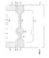
- the illustrated processforms an NPN HBT on a substrate 10 of FIG. 1 .
- the illustrated exemplary isolation processcomprises LOCOS (local oxidation of silicon) isolation regions 20 .
- LOCOSlocal oxidation of silicon
- other isolation structuressuch as shallow and deep trench isolation structures, can be used alone or in combination with the silicon dioxide isolation regions 20 .
- a silicon dioxide layer 26is formed over the substrate 10 between the isolation regions 20 .
- FIG. 1also illustrates a subcollector 30 formed within the substrate 10 by a dopant implant process through an appropriately patterned implant mask. A subsequent masking and implant operation forms an n-type lightly doped collector contact region 40 .
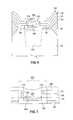
- a low-defect density germanium-enriched region 200(having a thickness of about 3 to 5 nanometers) is formed below an upper surface 190 of the silicon-germanium base 180 .
- Various oxidation process parameterse.g., duration, temperature and pressure
- a germanium enriched region 200approximately three to four nanometers thick is formed in the silicon-germanium base 180 with a thickness of approximately 120 nanometers.
- the germanium-enriched region 200ranges from a region 225 encompassing an area of the silicon-germanium base 180 exposed to the thermal oxide layer 185 , to a region 250 including the entire silicon-germanium base 180 .
- Silicon nitride spacers 260 and underlying silicon dioxide (TEOS) spacers 270are formed in the window 110 as illustrated in FIG. 10 .
- the spacerswhich serve to increase a distance between a later-formed emitter (having an n+ doping in an NPN transistor) and an extrinsic base (having a p+ doping in an NPN transistor) are formed by depositing a TEOS silicon dioxide layer and an overlying silicon nitride layer.
- the layersare anisotropically etched back to form the spacers 260 and 270 as illustrated, with the etch stopping on a region of the TEOS silicon dioxide layer formed on an upper surface of the base 180 .
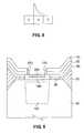
- a final HBT 300comprises a substantially defect-free germanium-enriched region 200 having a germanium concentration greater than is achievable by prior art standard epitaxial growth methods.
Landscapes
- Bipolar Transistors (AREA)
Abstract
Description
Claims (20)
Priority Applications (2)
| Application Number | Priority Date | Filing Date | Title |
|---|---|---|---|
| US12/728,412US8227319B2 (en) | 2004-03-10 | 2010-03-22 | Bipolar junction transistor having a high germanium concentration in a silicon-germanium layer and a method for forming the bipolar junction transistor |
| US13/348,415US20120115299A1 (en) | 2010-03-22 | 2012-01-11 | Bipolar junction transistor having a high germanium concentration in a silicon-germanium layer and a method for forming the bipolar junction transistor |
Applications Claiming Priority (4)
| Application Number | Priority Date | Filing Date | Title |
|---|---|---|---|
| US55230804P | 2004-03-10 | 2004-03-10 | |
| PCT/US2005/008212WO2005088721A1 (en) | 2004-03-10 | 2005-03-10 | A bipolar junction transistor having a high germanium concentration in a silicon-germanium layer and a method for forming the bipolar junction transistor |
| US10/598,213US7714361B2 (en) | 2004-03-10 | 2005-03-10 | Bipolar junction transistor having a high germanium concentration in a silicon-germanium layer and a method for forming the bipolar junction transistor |
| US12/728,412US8227319B2 (en) | 2004-03-10 | 2010-03-22 | Bipolar junction transistor having a high germanium concentration in a silicon-germanium layer and a method for forming the bipolar junction transistor |
Related Parent Applications (2)
| Application Number | Title | Priority Date | Filing Date |
|---|---|---|---|
| PCT/US2005/008212DivisionWO2005088721A1 (en) | 2004-03-10 | 2005-03-10 | A bipolar junction transistor having a high germanium concentration in a silicon-germanium layer and a method for forming the bipolar junction transistor |
| US10/598,213DivisionUS7714361B2 (en) | 2004-03-10 | 2005-03-10 | Bipolar junction transistor having a high germanium concentration in a silicon-germanium layer and a method for forming the bipolar junction transistor |
Related Child Applications (1)
| Application Number | Title | Priority Date | Filing Date |
|---|---|---|---|
| US13/348,415DivisionUS20120115299A1 (en) | 2010-03-22 | 2012-01-11 | Bipolar junction transistor having a high germanium concentration in a silicon-germanium layer and a method for forming the bipolar junction transistor |
Publications (2)
| Publication Number | Publication Date |
|---|---|
| US20110230031A1 US20110230031A1 (en) | 2011-09-22 |
| US8227319B2true US8227319B2 (en) | 2012-07-24 |
Family
ID=44647578
Family Applications (2)
| Application Number | Title | Priority Date | Filing Date |
|---|---|---|---|
| US12/728,412Expired - Fee RelatedUS8227319B2 (en) | 2004-03-10 | 2010-03-22 | Bipolar junction transistor having a high germanium concentration in a silicon-germanium layer and a method for forming the bipolar junction transistor |
| US13/348,415AbandonedUS20120115299A1 (en) | 2010-03-22 | 2012-01-11 | Bipolar junction transistor having a high germanium concentration in a silicon-germanium layer and a method for forming the bipolar junction transistor |
Family Applications After (1)
| Application Number | Title | Priority Date | Filing Date |
|---|---|---|---|
| US13/348,415AbandonedUS20120115299A1 (en) | 2010-03-22 | 2012-01-11 | Bipolar junction transistor having a high germanium concentration in a silicon-germanium layer and a method for forming the bipolar junction transistor |
Country Status (1)
| Country | Link |
|---|---|
| US (2) | US8227319B2 (en) |
Families Citing this family (4)
| Publication number | Priority date | Publication date | Assignee | Title |
|---|---|---|---|---|
| US8558282B1 (en)* | 2012-09-08 | 2013-10-15 | International Business Machines Corporation | Germanium lateral bipolar junction transistor |
| US9922941B1 (en)* | 2016-09-21 | 2018-03-20 | International Business Machines Corporation | Thin low defect relaxed silicon germanium layers on bulk silicon substrates |
| US20190097022A1 (en)* | 2017-09-28 | 2019-03-28 | International Business Machine Corporation | Method and structure to form vertical fin bjt with graded sige base doping |
| US11916136B2 (en) | 2022-02-25 | 2024-02-27 | Globalfoundries U.S. Inc. | Lateral bipolar junction transistors including a graded silicon-germanium intrinsic base |
Citations (14)
| Publication number | Priority date | Publication date | Assignee | Title |
|---|---|---|---|---|
| US3725161A (en) | 1971-03-03 | 1973-04-03 | A Kuper | Oxidation of semiconductive alloys and products obtained thereby |
| EP0435135A1 (en) | 1989-12-27 | 1991-07-03 | Texas Instruments Incorporated | A method of forming a Germanium layer and a heterojunction bipolar transistor formed therefrom |
| EP0490111A1 (en) | 1990-12-07 | 1992-06-17 | International Business Machines Corporation | A low capacitance bipolar junction transistor and fabrication process therefor |
| US5516724A (en)* | 1994-11-30 | 1996-05-14 | Cornell Research Foundation, Inc. | Oxidizing methods for making low resistance source/drain germanium contacts |
| EP0881669A1 (en) | 1997-05-30 | 1998-12-02 | STMicroelectronics S.r.l. | Manufacturing process of a germanium implanted HBT bipolar transistor |
| US20020109208A1 (en)* | 2001-02-12 | 2002-08-15 | Alexander Kalnitsky | Method of forming an NPN device |
| US6437376B1 (en) | 2000-03-01 | 2002-08-20 | Applied Micro Circuits Corporation | Heterojunction bipolar transistor (HBT) with three-dimensional base contact |
| US6586297B1 (en)* | 2002-06-01 | 2003-07-01 | Newport Fab, Llc | Method for integrating a metastable base into a high-performance HBT and related structure |
| US20030189239A1 (en) | 2002-04-09 | 2003-10-09 | Alexander Kalnitsky | Self-aligned NPN transistor with raised extrinsic base |
| US6686250B1 (en) | 2002-11-20 | 2004-02-03 | Maxim Integrated Products, Inc. | Method of forming self-aligned bipolar transistor |
| US20050191825A1 (en)* | 2002-07-09 | 2005-09-01 | Bruno Ghyselen | Methods for transferring a thin layer from a wafer having a buffer layer |
| WO2005088721A1 (en) | 2004-03-10 | 2005-09-22 | Agere Systems Inc. | A bipolar junction transistor having a high germanium concentration in a silicon-germanium layer and a method for forming the bipolar junction transistor |
| US20070170541A1 (en)* | 2002-04-15 | 2007-07-26 | Chui Chi O | High-k dielectric for thermodynamically-stable substrate-type materials |
| US20070254440A1 (en)* | 2005-02-24 | 2007-11-01 | Nicolas Daval | Thermal oxidation of a sige layer and applications thereof |
- 2010
- 2010-03-22USUS12/728,412patent/US8227319B2/ennot_activeExpired - Fee Related
- 2012
- 2012-01-11USUS13/348,415patent/US20120115299A1/ennot_activeAbandoned
Patent Citations (15)
| Publication number | Priority date | Publication date | Assignee | Title |
|---|---|---|---|---|
| US3725161A (en) | 1971-03-03 | 1973-04-03 | A Kuper | Oxidation of semiconductive alloys and products obtained thereby |
| EP0435135A1 (en) | 1989-12-27 | 1991-07-03 | Texas Instruments Incorporated | A method of forming a Germanium layer and a heterojunction bipolar transistor formed therefrom |
| EP0490111A1 (en) | 1990-12-07 | 1992-06-17 | International Business Machines Corporation | A low capacitance bipolar junction transistor and fabrication process therefor |
| US5516724A (en)* | 1994-11-30 | 1996-05-14 | Cornell Research Foundation, Inc. | Oxidizing methods for making low resistance source/drain germanium contacts |
| EP0881669A1 (en) | 1997-05-30 | 1998-12-02 | STMicroelectronics S.r.l. | Manufacturing process of a germanium implanted HBT bipolar transistor |
| US6437376B1 (en) | 2000-03-01 | 2002-08-20 | Applied Micro Circuits Corporation | Heterojunction bipolar transistor (HBT) with three-dimensional base contact |
| US20020109208A1 (en)* | 2001-02-12 | 2002-08-15 | Alexander Kalnitsky | Method of forming an NPN device |
| US20030189239A1 (en) | 2002-04-09 | 2003-10-09 | Alexander Kalnitsky | Self-aligned NPN transistor with raised extrinsic base |
| US20070170541A1 (en)* | 2002-04-15 | 2007-07-26 | Chui Chi O | High-k dielectric for thermodynamically-stable substrate-type materials |
| US6586297B1 (en)* | 2002-06-01 | 2003-07-01 | Newport Fab, Llc | Method for integrating a metastable base into a high-performance HBT and related structure |
| US20050191825A1 (en)* | 2002-07-09 | 2005-09-01 | Bruno Ghyselen | Methods for transferring a thin layer from a wafer having a buffer layer |
| US6686250B1 (en) | 2002-11-20 | 2004-02-03 | Maxim Integrated Products, Inc. | Method of forming self-aligned bipolar transistor |
| WO2005088721A1 (en) | 2004-03-10 | 2005-09-22 | Agere Systems Inc. | A bipolar junction transistor having a high germanium concentration in a silicon-germanium layer and a method for forming the bipolar junction transistor |
| US20080191245A1 (en) | 2004-03-10 | 2008-08-14 | Griglione Michelle D | Bipolar Junction Transistor Having A High Germanium Concentration In A Silicon-Germanium Layer And A Method For Forming The Bipolar Junction Transistor |
| US20070254440A1 (en)* | 2005-02-24 | 2007-11-01 | Nicolas Daval | Thermal oxidation of a sige layer and applications thereof |
Non-Patent Citations (4)
| Title |
|---|
| "Chem-Mech Polish for Self-Aligned Emitter/Base isolation in Single Poly Epi-Base Transistors"; IBM Technical Disclosure Bulletin, IBM Corp., vol. 35 No. 5 Oct. 1992; pp. 208-210 (XP 000312937). |
| LeGoues, F.K., et al.; "Oxidation Studies of SiGe"; J. Appl. Phys., vol. 65, No. 4, Feb. 15, 1989; pp. 1724-1728. |
| Lim, Y.S. et al.; "Dry Thermal Oxidation of a Graded SiGe Layer"; Applied Physics Letters, vol. 79, No. 22, Nov. 26, 2001; pp. 3606-3608. |
| Liou, H.K. et al.; "Effects of Ge Concentration of SiGe Oxidation Behavior"; Applied Physics Letters, American Institute of Physics, vol. 59, No. 10, Sep. 2, 1991; pp. 1200-1202 (XP 000324711). |
Also Published As
| Publication number | Publication date |
|---|---|
| US20120115299A1 (en) | 2012-05-10 |
| US20110230031A1 (en) | 2011-09-22 |
Similar Documents
| Publication | Publication Date | Title |
|---|---|---|
| JP5710714B2 (en) | Bipolar junction transistor having high concentration of germanium in silicon-germanium layer and method for forming the same | |
| US6417059B2 (en) | Process for forming a silicon-germanium base of a heterojunction bipolar transistor | |
| US6362065B1 (en) | Blocking of boron diffusion through the emitter-emitter poly interface in PNP HBTs through use of a SiC layer at the top of the emitter epi layer | |
| US5930635A (en) | Complementary Si/SiGe heterojunction bipolar technology | |
| US6509587B2 (en) | Semiconductor device | |
| US8541812B2 (en) | Semiconductor device and method of manufacture thereof | |
| JP4391069B2 (en) | Hetero bipolar transistor and manufacturing method thereof | |
| US7786510B2 (en) | Transistor structure and manufacturing method thereof | |
| JP2003297844A (en) | Semiconductor device and method of manufacturing semiconductor device | |
| JPH05182980A (en) | Heterojunction bipolar transistor | |
| US6861324B2 (en) | Method of forming a super self-aligned hetero-junction bipolar transistor | |
| US8227319B2 (en) | Bipolar junction transistor having a high germanium concentration in a silicon-germanium layer and a method for forming the bipolar junction transistor | |
| US9064886B2 (en) | Heterojunction bipolar transistor having a germanium extrinsic base utilizing a sacrificial emitter post | |
| US7511317B2 (en) | Porous silicon for isolation region formation and related structure | |
| US6573539B2 (en) | Heterojunction bipolar transistor with silicon-germanium base | |
| JP3515944B2 (en) | Hetero bipolar transistor | |
| US20040115878A1 (en) | Method for manufacturing a silicon germanium based device with crystal defect prevention | |
| US10529836B1 (en) | SiGe heterojunction bipolar transistor with crystalline raised base on germanium etch stop layer | |
| JP3159527B2 (en) | Method for manufacturing semiconductor device | |
| JPH06260492A (en) | Bipolar transistor manufacturing method | |
| JP2005033080A (en) | Semiconductor device and manufacturing method thereof | |
| JP2001118854A (en) | Method for manufacturing semiconductor device |
Legal Events
| Date | Code | Title | Description |
|---|---|---|---|
| AS | Assignment | Owner name:AGERE SYSTEMS INC., PENNSYLVANIA Free format text:ASSIGNMENT OF ASSIGNORS INTEREST;ASSIGNOR:GRIGLIONE, MICHELLE D.;REEL/FRAME:024113/0706 Effective date:20060818 | |
| STCF | Information on status: patent grant | Free format text:PATENTED CASE | |
| AS | Assignment | Owner name:DEUTSCHE BANK AG NEW YORK BRANCH, AS COLLATERAL AG Free format text:PATENT SECURITY AGREEMENT;ASSIGNORS:LSI CORPORATION;AGERE SYSTEMS LLC;REEL/FRAME:032856/0031 Effective date:20140506 | |
| AS | Assignment | Owner name:AVAGO TECHNOLOGIES GENERAL IP (SINGAPORE) PTE. LTD Free format text:ASSIGNMENT OF ASSIGNORS INTEREST;ASSIGNOR:AGERE SYSTEMS LLC;REEL/FRAME:035365/0634 Effective date:20140804 | |
| FPAY | Fee payment | Year of fee payment:4 | |
| AS | Assignment | Owner name:LSI CORPORATION, CALIFORNIA Free format text:TERMINATION AND RELEASE OF SECURITY INTEREST IN PATENT RIGHTS (RELEASES RF 032856-0031);ASSIGNOR:DEUTSCHE BANK AG NEW YORK BRANCH, AS COLLATERAL AGENT;REEL/FRAME:037684/0039 Effective date:20160201 Owner name:AGERE SYSTEMS LLC, PENNSYLVANIA Free format text:TERMINATION AND RELEASE OF SECURITY INTEREST IN PATENT RIGHTS (RELEASES RF 032856-0031);ASSIGNOR:DEUTSCHE BANK AG NEW YORK BRANCH, AS COLLATERAL AGENT;REEL/FRAME:037684/0039 Effective date:20160201 | |
| AS | Assignment | Owner name:BANK OF AMERICA, N.A., AS COLLATERAL AGENT, NORTH CAROLINA Free format text:PATENT SECURITY AGREEMENT;ASSIGNOR:AVAGO TECHNOLOGIES GENERAL IP (SINGAPORE) PTE. LTD.;REEL/FRAME:037808/0001 Effective date:20160201 Owner name:BANK OF AMERICA, N.A., AS COLLATERAL AGENT, NORTH Free format text:PATENT SECURITY AGREEMENT;ASSIGNOR:AVAGO TECHNOLOGIES GENERAL IP (SINGAPORE) PTE. LTD.;REEL/FRAME:037808/0001 Effective date:20160201 | |
| AS | Assignment | Owner name:AVAGO TECHNOLOGIES GENERAL IP (SINGAPORE) PTE. LTD., SINGAPORE Free format text:TERMINATION AND RELEASE OF SECURITY INTEREST IN PATENTS;ASSIGNOR:BANK OF AMERICA, N.A., AS COLLATERAL AGENT;REEL/FRAME:041710/0001 Effective date:20170119 Owner name:AVAGO TECHNOLOGIES GENERAL IP (SINGAPORE) PTE. LTD Free format text:TERMINATION AND RELEASE OF SECURITY INTEREST IN PATENTS;ASSIGNOR:BANK OF AMERICA, N.A., AS COLLATERAL AGENT;REEL/FRAME:041710/0001 Effective date:20170119 | |
| AS | Assignment | Owner name:BELL SEMICONDUCTOR, LLC, ILLINOIS Free format text:ASSIGNMENT OF ASSIGNORS INTEREST;ASSIGNORS:AVAGO TECHNOLOGIES GENERAL IP (SINGAPORE) PTE. LTD.;BROADCOM CORPORATION;REEL/FRAME:044886/0001 Effective date:20171208 | |
| AS | Assignment | Owner name:CORTLAND CAPITAL MARKET SERVICES LLC, AS COLLATERA Free format text:SECURITY INTEREST;ASSIGNORS:HILCO PATENT ACQUISITION 56, LLC;BELL SEMICONDUCTOR, LLC;BELL NORTHERN RESEARCH, LLC;REEL/FRAME:045216/0020 Effective date:20180124 | |
| MAFP | Maintenance fee payment | Free format text:PAYMENT OF MAINTENANCE FEE, 8TH YEAR, LARGE ENTITY (ORIGINAL EVENT CODE: M1552); ENTITY STATUS OF PATENT OWNER: LARGE ENTITY Year of fee payment:8 | |
| AS | Assignment | Owner name:BELL NORTHERN RESEARCH, LLC, ILLINOIS Free format text:SECURITY INTEREST;ASSIGNOR:CORTLAND CAPITAL MARKET SERVICES LLC;REEL/FRAME:060885/0001 Effective date:20220401 Owner name:BELL SEMICONDUCTOR, LLC, ILLINOIS Free format text:SECURITY INTEREST;ASSIGNOR:CORTLAND CAPITAL MARKET SERVICES LLC;REEL/FRAME:060885/0001 Effective date:20220401 Owner name:HILCO PATENT ACQUISITION 56, LLC, ILLINOIS Free format text:SECURITY INTEREST;ASSIGNOR:CORTLAND CAPITAL MARKET SERVICES LLC;REEL/FRAME:060885/0001 Effective date:20220401 | |
| FEPP | Fee payment procedure | Free format text:MAINTENANCE FEE REMINDER MAILED (ORIGINAL EVENT CODE: REM.); ENTITY STATUS OF PATENT OWNER: LARGE ENTITY | |
| LAPS | Lapse for failure to pay maintenance fees | Free format text:PATENT EXPIRED FOR FAILURE TO PAY MAINTENANCE FEES (ORIGINAL EVENT CODE: EXP.); ENTITY STATUS OF PATENT OWNER: LARGE ENTITY | |
| STCH | Information on status: patent discontinuation | Free format text:PATENT EXPIRED DUE TO NONPAYMENT OF MAINTENANCE FEES UNDER 37 CFR 1.362 | |
| FP | Lapsed due to failure to pay maintenance fee | Effective date:20240724 |