US8227305B2 - Memory array with ultra-thin etched pillar surround gate access transistors and buried data/bit lines - Google Patents
Memory array with ultra-thin etched pillar surround gate access transistors and buried data/bit linesDownload PDFInfo
- Publication number
- US8227305B2 US8227305B2US13/050,819US201113050819AUS8227305B2US 8227305 B2US8227305 B2US 8227305B2US 201113050819 AUS201113050819 AUS 201113050819AUS 8227305 B2US8227305 B2US 8227305B2
- Authority
- US
- United States
- Prior art keywords
- pillar
- forming
- gate structure
- generally
- access transistors
- Prior art date
- Legal status (The legal status is an assumption and is not a legal conclusion. Google has not performed a legal analysis and makes no representation as to the accuracy of the status listed.)
- Expired - Lifetime
Links
Images


Classifications
- H—ELECTRICITY
- H10—SEMICONDUCTOR DEVICES; ELECTRIC SOLID-STATE DEVICES NOT OTHERWISE PROVIDED FOR
- H10B—ELECTRONIC MEMORY DEVICES
- H10B12/00—Dynamic random access memory [DRAM] devices
- H10B12/01—Manufacture or treatment
- H10B12/02—Manufacture or treatment for one transistor one-capacitor [1T-1C] memory cells
- H10B12/05—Making the transistor
- H10B12/053—Making the transistor the transistor being at least partially in a trench in the substrate
- H—ELECTRICITY
- H10—SEMICONDUCTOR DEVICES; ELECTRIC SOLID-STATE DEVICES NOT OTHERWISE PROVIDED FOR
- H10B—ELECTRONIC MEMORY DEVICES
- H10B12/00—Dynamic random access memory [DRAM] devices
- H10B12/30—DRAM devices comprising one-transistor - one-capacitor [1T-1C] memory cells
- H10B12/48—Data lines or contacts therefor
- H10B12/482—Bit lines
- H—ELECTRICITY
- H10—SEMICONDUCTOR DEVICES; ELECTRIC SOLID-STATE DEVICES NOT OTHERWISE PROVIDED FOR
- H10D—INORGANIC ELECTRIC SEMICONDUCTOR DEVICES
- H10D30/00—Field-effect transistors [FET]
- H10D30/01—Manufacture or treatment
- H10D30/021—Manufacture or treatment of FETs having insulated gates [IGFET]
- H10D30/025—Manufacture or treatment of FETs having insulated gates [IGFET] of vertical IGFETs
- H—ELECTRICITY
- H10—SEMICONDUCTOR DEVICES; ELECTRIC SOLID-STATE DEVICES NOT OTHERWISE PROVIDED FOR
- H10D—INORGANIC ELECTRIC SEMICONDUCTOR DEVICES
- H10D30/00—Field-effect transistors [FET]
- H10D30/60—Insulated-gate field-effect transistors [IGFET]
- H10D30/63—Vertical IGFETs
- H—ELECTRICITY
- H10—SEMICONDUCTOR DEVICES; ELECTRIC SOLID-STATE DEVICES NOT OTHERWISE PROVIDED FOR
- H10B—ELECTRONIC MEMORY DEVICES
- H10B12/00—Dynamic random access memory [DRAM] devices
- H10B12/30—DRAM devices comprising one-transistor - one-capacitor [1T-1C] memory cells
- H10B12/48—Data lines or contacts therefor
- H10B12/488—Word lines
Definitions
- the inventionrelates to the field of high density semiconductor memory arrays and more particularly to arrays with vertical transistors having sub-photolithographic device dimensions with ultra-thin pillars and substantially fully surrounding gates suitable for use as access transistors, such as for DRAM arrays.
- junction depthshould be much less than the channel length, and thus for a channel length of, for example, 1,000 ⁇ , this implies junction depths on the order of a few hundred Angstroms. Such shallow junctions are difficult to form by conventional implantation and diffusion techniques.
- FIG. 1illustrates general trends and relationships for a variety of device parameters with scaling by a factor k.
- DIBLdrain induced barrier lowering
- DRAMdynamic random access memory
- Extremely high doping levelgenerally results in increased leakage and reduced carrier mobility, thus making the channel shorter to improve performance is offset or negated by the lower carrier mobility and higher leakage. This leakage current is a significant concern and problem in low voltage and low power battery operated complimentary metal oxide semiconductor (CMOS) circuits and systems, particularly in DRAMs.
- CMOScomplimentary metal oxide semiconductor
- threshold voltage magnitudesare desirably small, in this example near 0 volts, however then the transistor, such as an access transistor, will always have a large sub-threshold leakage current.
- CMOS transistorsthat can have relatively large variations in threshold voltage, yet still have relatively low sub-threshold leakage currents at standby.
- dual-gated or double-gated transistor structuresFor example, one technique used in scaling down transistors is referred to as dual-gated or double-gated transistor structures.
- the terminology generally employed in the industryis “dual-gate” if the transistor has a front gate and a back gate which can be driven with separate and independent voltages and “double-gated” to describe structures where both gates are driven with the same potential.
- a dual-gated and/or double-gated MOSFEToffers better device characteristics than conventional bulk silicon MOSFETs. Because a gate electrode is present on both sides of the channel, rather than only on one side as in conventional planar MOSFETs, the electrical field generated by the drain electrode is better screened from the source end of the channel than in conventional planar MOSFETs, as illustrated schematically by the field lines in FIG. 3 .
- a memory arraycomprising a semiconductive substrate, a plurality of conductive data/bit lines extending generally in a first direction and formed in an upper surface of the substrate, a plurality of access transistors extending generally upward from the upper surface of the substrate and aligned generally atop a corresponding data/bit line, wherein the access transistors comprise a pillar extending generally upward from the upper surface of the substrate and generally aligned atop the corresponding data/bit line wherein a source region is formed generally at a lower portion of the pillar so as to be in electrical communication with the corresponding data/bit line and a drain region is formed generally at an upper portion of the pillar, wherein the pillar intermediate the source and drain regions is substantially fully depleted and a surround gate structure substantially completely encompassing the pillar in lateral directions and extending substantially the entire vertical extent of the pillar, and a plurality of conductive word lines extending generally in a second direction and in electrical contact with a corresponding surround gate
- Another embodimentis a method of fabricating a memory array comprising forming a plurality of data/bit lines in a surface of a substrate so as to extend in a first direction, forming a first mask layer on the surface of the substrate, forming first elongate openings in the first mask layer so as to be aligned generally with and extending along corresponding data/bit lines, depositing sidewall material in the first openings of the first mask layer, directionally etching the sidewall material so as to form first sidewall spacers arranged against inner surfaces of the first openings and defining generally centrally arranged first trenches in the first sidewall spacers between opposed sidewall spacers, forming first plug strips in corresponding first trenches, performing a directional etch with the first plug strips as masking structures so as to define a corresponding plurality of pillar strips extending generally vertically from the surface of the substrate and substantially conforming to the contour and position of the first plug strips, filling interstitial spaces between the pillar strips with fill material, forming a second
- a further embodimentis a method of fabricating a memory array comprising forming a plurality of data/bit lines in a surface of a substrate, forming a mask layer on the surface of the substrate, forming openings in the mask layer so as to be aligned generally with corresponding data/bit lines, depositing sidewall material in the openings of the mask layer, directionally etching the sidewall material so as to form sidewall structures arranged against inner surfaces of the openings and defining a generally centrally arranged hole in the sidewall structures, forming a plug structure in the holes, performing a directional etch with the plug structures as masking structures so as to define a plurality of pillars extending generally vertically from the surface of the substrate and substantially conforming to the contour and position of the plug structures, and forming gate structures about the pillars such that the gate structures substantially completely encompass corresponding pillars.
- various embodimentsprovide a memory array including access transistors over buried data/bit lines which include substantially surrounding gate structures which provide improved sub-threshold performance and relatively high device density. Certain embodiments provide the ability to fabricate relatively precisely defined device features of sub-photolithographic dimensions. Embodiments also provide word lines that contact surround gate structures for improved control of the conduction channel.
- FIG. 1is schematic illustration of general relationships of various device parameters/characteristics for a scaling factor k;
- FIG. 2is a graph illustrating sub-threshold leakage in a conventional silicon MOSFET
- FIG. 3is a schematic illustration of a known dual-gate MOSFET
- FIG. 4is a graph illustrating sub-threshold conduction characteristics of conventional bulk silicon MOSFETs and of dual-gate and/or double gate MOSFETs;
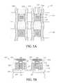
- FIG. 5Ais a top section view along A-A′ of FIG. 5B which is a side section view both of one embodiment of an array of ultra-thin etched pillar access transistors;
- FIG. 6is a perspective view of the embodiments shown in section in FIGS. 5A and 5B ;
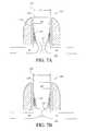
- FIG. 7Ais a side section view of one embodiment of an access transistor in a memory array and illustrating schematically electrical operation thereof;
- FIG. 7Bis a side section view of another embodiment of an access transistor in a memory array and illustrating schematically electrical operation thereof;
- FIGS. 8A-11Aare top views and FIGS. 8B-11B are side section views respectively of one embodiment of fabricating an ultra-thin body transistor
- FIGS. 12A-16Aare top views and FIGS. 12B-16B are end section views respectively of another embodiment of fabricating an ultra-thin body transistor
- FIG. 17is a top view of a further fabrication step in one embodiment of fabricating an ultra-thin body transistor
- FIG. 18is a perspective view of yet a further step in one embodiment of fabricating an ultra-thin body transistor
- FIGS. 19A and 19Bare side section and top views respectively of one embodiment of a method of forming surround gate structures.
- FIGS. 20A and 20Bare side section and top views respectively of one embodiment of a method of forming word/address lines in enclosing contact with the surround gate structures.
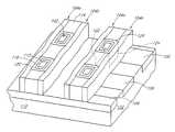
- FIGS. 5A , 5 B, and 6illustrate a top section view, side section view, and perspective view respectively of one embodiment of a memory circuit access array 100 , which in following will be referred to as the array 100 for brevity.
- the array 100provides access with a plurality of memory cells, in certain embodiments an array of DRAM cells, which can be utilized for storage and access of information.
- the array 100comprises a plurality of access transistors 102 , each of which is in electrical communication with a corresponding word line 104 and data/bit line 106 .
- the word lines 104are arranged generally parallel to each other.
- the data/bit linesare as well arranged substantially in parallel with each other, and also extending generally transversely with respect to the word lines 104 .
- a pair of word lines 104 a and 104 bare provided for any given access transistor 102 and are arranged on opposite sides of each access transistor 102 .
- the array 100is formed on top of a semiconductive substrate 110 , in one particular embodiment comprising silicon. As can be seen in the side section view of FIG. 5B , the data/bit lines 106 extend across an upper surface of the substrate 110 . In certain embodiments, the data/bit lines 106 comprise doped silicon regions of the substrate 110 and in one particular embodiment, n+ doped silicon.
- the array 100also comprises a plurality of generally vertically extending ultra thin semiconductive pillars 112 forming a part of the structure of each access transistor 102 and positioned generally aligned with and atop corresponding buried data/bit lines 106 .
- An insulator layer 114is positioned atop the substrate 110 and interposed portions of the data/bit lines 106 and includes gate insulator regions 116 which, in this embodiment, extend generally upward and substantially circumferentially enclose or encompass each of the semiconductive pillars 112 .
- the semiconductive pillars 112are generally configured as ultra-thin vertically extending posts, cylinders, prisms, or the like
- the respective gate insulator regions 116are configured as corresponding hollow posts, pillars, cylinders, prisms, or the like with the inner surface of the gate insulator region 116 conforming in cross-section to the outer surface of the respective semiconductive pillar 112 such that the two are in contact with each other.
- the array 100comprises a corresponding plurality of gate conductor structures 120 which are also configured as generally vertically extending structures substantially encompassing or encircling and overlaid about the respective gate insulator region 116 with the enclosed semiconductive pillar 112 .
- the gate conductors 120comprise polycrystalline silicon (polysilicon).
- the gate conductors 120are arranged with respect to corresponding word lines 104 a and 104 b , such that the gate conductor 120 is in electrical contact with the respective word line 104 a along a first contact surface 122 , and such that the gate conductor 120 is in electrical contact with the respective word line 104 b along a second contact surface 124 which is arranged substantially opposite the first contact surface 122 .
- the word lines 104 a and 104 bcomprise conductive material which is in electrical contact with the gate conductor 120 , also comprising electrically conductive material, along the opposed first and second contact surfaces 122 , 124 .
- electrical potential which is provided via the word lines 104 a , 104 bwill thus be conducted via the gate conductor 120 so as to substantially encompass or encircle the gate insulator region 116 and semiconductive pillar 112 which are arranged within the interior of the gate conductor 120 .
- the electric potential/field within the pillars 112will be substantially laterally or horizontally symmetric at a given vertical position of the pillar 112 (see FIGS. 7A and 7B ).
- a surround gate structure 126is defined wherein an electrical potential can be provided substantially encircling or encompassing the enclosed semiconductive pillar 112 , however wherein the gate insulator region 116 inhibits electrical conduction therebetween.
- This surround gate structure 126( FIG. 6 ), by providing regulated electrical potential via the word lines 104 a and 104 b and further via the gate conductor 120 about substantially all lateral sides, faces, directions of the generally vertically extending semiconductive pillar 112 , provides even more control of a gate potential applied to/removed from the pillar 112 as opposed to only a single side of a gate as in conventional bulk silicon processes and devices or the opposed sides of a dual gate and/or double gate MOSFET structure.
- the doping of the pillars 112is such that the transistors 102 operate from a substantially fully depleted state.
- absence of an applied potential to the surround gate structure 126substantially removes a conduction channel 134 ( FIGS. 7A and 7B ) thereby avoiding the need to apply a potential to turn off the transistors 102 .
- This embodimentprovides simplified and more convenient operation of the array 100 and facilitates integration with other systems.
- FIGS. 7A and 7Billustrate in side section view in greater detail embodiments of portions of the array 100 including the access transistors 102 thereof.
- FIG. 7Aillustrates one embodiment of the access transistor 102 , wherein the pillar 112 has a thickness 128 indicated as t 1 and similarly for FIG. 7B the pillar 112 having a pillar thickness 128 t 2 . While the illustrations herein are schematic in nature and should not be interpreted as being to scale, in these embodiments, the pillar thickness 128 t 1 is greater than the pillar thickness 128 t 2 .
- the pillar thickness 128 referred tocan comprise multiple laterally-extending thickness measurements, such as in embodiments wherein the pillar 112 defines generally a rectangular prism structure, or generally a single lateral diameter dimension in embodiments wherein the pillar 112 defines generally a cylindrical vertically-extending structure.
- drain regions 130are defined generally adjacent the upper extent of the pillars 112 and source regions 132 positioned generally adjacent the lower extent of the pillars 112 .
- the drain region 130 and source region 132comprise regions of the semiconductive pillar 112 which are doped n+.
- the surround gate structure 126when the access transistor 102 is in an off condition, the surround gate structure 126 will be at substantially a zero or a negative bias.
- the access transistor 102 of these embodimentsoffers better device characteristics than conventional bulk silicon MOSFETs. These improved device characteristics arise because the thin physical dimensions of the ultra-thin semiconductive pillars 112 facilitate full depletion of the transistor 102 with relatively low doping levels.
- a major pillar thickness 128 of approximately 100 nm with doping density of approximately 1 ⁇ 10 15 /cm 3provides the transistor 102 with substantially full depletion characteristics.
- embodiments of the array 100offer increased circuit density with individual transistors 102 having relatively low doping densities in the pillars 112 thereof which reduces the aforementioned problems with relatively high doping levels which would otherwise be indicated to mitigate short channel effects.
- the surround gate structure 126encloses all lateral sides of a conduction channel 134 rather than only on one side as in conventional MOSFETs or separate opposed sides as in a dual gate and/or double gate MOSFET, more effective control of the channel is provided.
- the conduction channels 134 of these embodimentswill describe generally a vertically extending annulus or ring structure conforming generally to the cross-sectional contour of the corresponding semiconductive pillar 112 .
- the conduction channels 134are substantially horizontally symmetric at a given vertical position of the pillars 112 .
- this leakage currentis a significant device parameter of the memory array 100 , particularly when the array 100 is configured as an array of DRAMs.
- the subthreshold and leakage currentis a significant variable in determining the maximum retention time and the corresponding requirements for refreshing of logic states stored in the array 100 and the corresponding time or intervals between required refresh operations.
- the surround gate structure 126is biased positive to a value based on the particular application, however generally on the order of a few tenths of a volt.
- the source region 132may or may not substantially extend across the lower extent of the semiconductive pillar 112 .
- the source region 132would not extend entirely across the lower extent of the semiconductive pillar 112 .
- the embodiment illustrated by FIG. 7Awherein the pillar thickness 128 is somewhat thicker as indicated by t 1 , the source region 132 would not extend entirely across the lower extent of the semiconductive pillar 112 .
- the pillar thickness 128is relatively thinner or narrower indicated as T 2 , and in this embodiment, the source region 132 would extend substantially across the bottom or lower extent of the semiconductive pillar 112 . As the source region 132 of the embodiment illustrated in FIG. 7B extends across the base of the pillar 112 and thus provides a full p/n junction across the lower extent of the pillar 112 , this embodiment is generally preferred. Because the pillar thickness 128 is relatively small, application of high temperature processes to induce lateral diffusion of implanted dopants to form the source regions 132 is reduced, thereby avoiding the problematic aspects of more extreme high temperature parameters such as would be required with wide pillar structures. For example, in one embodiment, the array 100 is formed with high temperature process parameters not exceeding approximately 800° C. and 10 minutes. Embodiments of fabrication of the array 100 will be described in greater detail below.
- FIGS. 8A and 8B through 11 A and 11 Billustrate schematically one embodiment of methods 200 of forming ultra thin body transistors, such as the access transistors 102 previously described, wherein the transistors 102 have sub-lithographic dimensions.
- the transistors 102are formed by a side wall spacer technique described in greater detail below.
- a mask material 202is formed on top of the underlying substrate 110 and an opening 204 is formed in the mask layer 202 so as to expose a portion of the underlying substrate 110 .
- the opening 204is formed generally to conform to the desired cross-sectional shape of the surround gate structure 126 and semiconductive pillar 112 .
- a generally square-shaped opening 204is illustrated, this is for ease of illustration and is only one of many possible shapes of the opening 204 .
- spacer materialin one embodiment comprising silicon oxide, is deposited within the opening 204 of the mask layer 202 .
- This spacer materialis subjected to an anisotropic etch 206 so as to form a sidewall spacer structure 210 positioned generally against inner surfaces of the opening 204 formed in the mask layer 202 and further so as to form a generally centrally positioned hole 212 generally in the center of the sidewall spacer structure 210 and the opening 204 .
- a pillar plug 214is formed within the generally centrally located hole 212 in the sidewall spacer structure 210 .
- the pillar plug 214comprises silicon nitride which is deposited, planarized, and etched so as to partially recess the pillar plug 214 within the hole 212 .
- This pillar plug 214is subsequently utilized as a masking structure for etching of the underlying substrate 110 so as to define the semiconductive pillars 112 .
- the profile and dimensions of the pillar plug 214generally corresponds to the subsequently formed semiconductive pillars 112 .
- the mask 202 and side wall spacer structure 210are removed so as to leave the pillar plug 214 .
- An etch 216is performed to remove portions of the upper surface of the substrate 110 with the pillar plug 214 as a masking structure.
- the vertically extending pillar 112is defined extending upwards from the upper surface of the substrate 110 .
- FIGS. 12A-16A , 12 B- 16 B, 17 , and 18illustrate steps of another embodiment of a method 300 for forming pillars 112 for the ultra thin body transistors 102 .
- a mask layer 302is formed on top of the underlying substrate 110 and a generally elongate first mask opening 304 is formed therein.
- certain steps of the method 300will be illustrated with respect to formation of a single semiconductive pillar 112 , however, it will be understood that generally the method 300 would be employed to fabricate a plurality of the pillars 112 so as to subsequently define the array 100 .
- a first mask layer 302is formed on the substrate 110 with a plurality of first openings 304 formed therein so as to expose generally parallel elongate trenchlike structures.
- sidewall materialis formed within the first opening 304 and exposed to an anisotropic etch 306 so as to define first sidewall spacers 310 which also extend in an elongate manner generally along the sides of the first opening 304 formed in the mask layer 302 .
- the anisotropic etch 306further defines a first central trench 312 which similarly extends in an elongate manner between opposed sidewall spacers 310 .
- a first plug strip 314is formed within the first central trench 312 and in one particular embodiment comprises silicon nitride which is deposited, planarized, and etched so as to form the first plug strip 314 generally in a similar manner to that previously described for the pillar plug 214 of the method 200 .
- an etch 316is performed employing the first plug strip 314 as a masking structure so as to define a plurality of underlying generally vertically extending pillar strips 320 , which are elongate extending generally upward from the substrate 110 and corresponding generally to the contour and dimensions of the first plug strips 314 .
- the first plug strips 314are removed, and the spaces between the first pillar strips 320 and above the substrate 110 are formed with a fill material 322 which, in one embodiment, comprises a back filling with silicon oxide.
- the preceding steps of the method 300are repeated substantially as previously described, however with the difference that the structures previously described, such as the first pillar strips 320 , are formed aligned generally along a first direction 322 and the following structures are fabricated oriented generally along a perpendicularly arranged second direction 326 .
- a second mask layer 332is formed with a second opening 334 formed to extend generally in the second direction 326 .
- These structuresare formed to overly the previously formed pillar strips 320 and fill material 322 which are illustrated in dashed lines and with parenthetical reference numbers.
- a sidewall materialis formed within the second opening 334 and exposed to an anisotropic etch 336 so as to define second sidewall spacers 340 and a second central trench 342 positioned generally between the opposed sidewall spacers 340 , again with these structures oriented generally in the second direction 326 .
- the second central trench 342is again filled with material so as to form a second plug strip 344 , again extending generally along the second direction 326 .
- an etch 346is performed employing the second plug strip 344 as a masking structure.
- the second plug strip 344extends generally along the second direction 326 and overlies the previously formed pillar strips 320 extending generally in the first direction 324 .
- the excess material of the first pillar strips 320 not masked by the intersecting second plug strip 344is removed during the etch process 346 so as to define a corresponding plurality of generally vertically extending semiconductive pillars 112 extending generally vertically upward from the underlying substrate 110 .
- the size and configuration of the resultant semiconductive pillars 112corresponds to the intersection envelope between the first plug strips 314 and second plug strips 344 .
- the embodiments of the method 300may provide advantages compared to the embodiments of the method 200 as the profile of the resultant semiconductive pillars 112 is defined by the intersection of the edges of the first plug strip 314 and second plug strip 344 which are configured as elongate strips rather than the single pillar plugs 214 of the method 200 .
- edgesmay be more precisely defined than the contour of individual holes, such as the central hole 212 .
- FIGS. 19A , 19 B, 20 A, and 20 Billustrate the further fabrication of the surround gate structures 126 and word lines 104 in this embodiment in a side wall spacer based process.
- the respective pillars 112define a device to device spacing 136 , separated by a distance 2 F as shown.
- the pillars 112also define a pillar thickness 128 indicated by t in FIG. 15 .
- the pillar thickness 128is much less than the photolithographic dimension limit F, and thus the array 100 defines device features, such as the pillar thickness 128 , which are below the photolithographic dimension F.
- the gate insulator region 116is grown or deposited and then polysilicon is further deposited on the gate insulator regions 116 .
- An anisotropic etch 140is then performed so as to define sidewall structures of the encompassing gate insulator region 116 and surrounding gate conductor 120 .
- this structureis back filled, such as with the insulator layer 114 comprising oxide.
- Trenches 142are formed in this back fill material, such as the insulator layer 114 , wherein the trenches are interposed between adjacent transistors 102 and in one particular embodiment, extending generally in the second direction 326 .
- polysilicon or metalis deposited and anisotropically etched so as to be in contact generally at the first surface 122 and opposed second surface 124 defining the word/address lines 104 a and 104 b .
- the remainder of the process to form the array 100for example, establishment of capacitor contacts 144 and formation of cap/passivation structures 146 as shown in FIG. 20B (also FIG. 5B ) can be formed using conventional techniques well understood by one of ordinary skill in the art. It will also be understood that certain intermediate processes, such as implants/diffusion processes for example to dope the pillars 112 and form the drain 130 and source 132 regions to form the array 100 will also be well understood by one of ordinary skill.
- the aforementioned embodimentsdescribe methods 200 and 300 for forming an array 100 of memory cells, such as an array of DRAM cells, having access transistors 102 with semiconductive pillars 112 of ultra thin dimensions.
- the device dimensionssuch as the pillar thickness 128
- a photolithographic process limit Fproviding particularly efficient and densely packed components of the array 100 .
- Further advantages of the embodiments described hereinare the formation of a surround gate structure 126 which provides more effective control of the conduction channel 134 with the aggressive scaling provided by these embodiments.
- certain embodimentsprovide a substantially fully depleted pillar 112 structure of ultra-thin dimensions which reduces the need for extremely high doping levels to reduce short channel effects and the attendant problems of high doping levels.
Landscapes
- Engineering & Computer Science (AREA)
- Manufacturing & Machinery (AREA)
- Semiconductor Memories (AREA)
- Insulated Gate Type Field-Effect Transistor (AREA)
Abstract
Description
Claims (20)
Priority Applications (2)
| Application Number | Priority Date | Filing Date | Title |
|---|---|---|---|
| US13/050,819US8227305B2 (en) | 2005-05-13 | 2011-03-17 | Memory array with ultra-thin etched pillar surround gate access transistors and buried data/bit lines |
| US13/548,614US8637362B2 (en) | 2005-05-13 | 2012-07-13 | Memory array with ultra-thin etched pillar surround gate access transistors and buried data/bit lines |
Applications Claiming Priority (4)
| Application Number | Priority Date | Filing Date | Title |
|---|---|---|---|
| US11/129,502US7371627B1 (en) | 2005-05-13 | 2005-05-13 | Memory array with ultra-thin etched pillar surround gate access transistors and buried data/bit lines |
| US11/457,423US7525141B1 (en) | 2005-05-13 | 2006-07-13 | Memory array with ultra-thin etched pillar surround gate access transistors and buried data/bit lines |
| US12/407,615US7910972B2 (en) | 2005-05-13 | 2009-03-19 | Memory array with ultra-thin etched pillar surround gate access transistors and buried data/bit lines |
| US13/050,819US8227305B2 (en) | 2005-05-13 | 2011-03-17 | Memory array with ultra-thin etched pillar surround gate access transistors and buried data/bit lines |
Related Parent Applications (1)
| Application Number | Title | Priority Date | Filing Date |
|---|---|---|---|
| US12/407,615ContinuationUS7910972B2 (en) | 2005-05-13 | 2009-03-19 | Memory array with ultra-thin etched pillar surround gate access transistors and buried data/bit lines |
Related Child Applications (1)
| Application Number | Title | Priority Date | Filing Date |
|---|---|---|---|
| US13/548,614ContinuationUS8637362B2 (en) | 2005-05-13 | 2012-07-13 | Memory array with ultra-thin etched pillar surround gate access transistors and buried data/bit lines |
Publications (2)
| Publication Number | Publication Date |
|---|---|
| US20110165744A1 US20110165744A1 (en) | 2011-07-07 |
| US8227305B2true US8227305B2 (en) | 2012-07-24 |
Family
ID=39361587
Family Applications (5)
| Application Number | Title | Priority Date | Filing Date |
|---|---|---|---|
| US11/129,502Expired - LifetimeUS7371627B1 (en) | 2005-05-13 | 2005-05-13 | Memory array with ultra-thin etched pillar surround gate access transistors and buried data/bit lines |
| US11/457,423Active2026-01-22US7525141B1 (en) | 2005-05-13 | 2006-07-13 | Memory array with ultra-thin etched pillar surround gate access transistors and buried data/bit lines |
| US12/407,615Expired - LifetimeUS7910972B2 (en) | 2005-05-13 | 2009-03-19 | Memory array with ultra-thin etched pillar surround gate access transistors and buried data/bit lines |
| US13/050,819Expired - LifetimeUS8227305B2 (en) | 2005-05-13 | 2011-03-17 | Memory array with ultra-thin etched pillar surround gate access transistors and buried data/bit lines |
| US13/548,614Expired - LifetimeUS8637362B2 (en) | 2005-05-13 | 2012-07-13 | Memory array with ultra-thin etched pillar surround gate access transistors and buried data/bit lines |
Family Applications Before (3)
| Application Number | Title | Priority Date | Filing Date |
|---|---|---|---|
| US11/129,502Expired - LifetimeUS7371627B1 (en) | 2005-05-13 | 2005-05-13 | Memory array with ultra-thin etched pillar surround gate access transistors and buried data/bit lines |
| US11/457,423Active2026-01-22US7525141B1 (en) | 2005-05-13 | 2006-07-13 | Memory array with ultra-thin etched pillar surround gate access transistors and buried data/bit lines |
| US12/407,615Expired - LifetimeUS7910972B2 (en) | 2005-05-13 | 2009-03-19 | Memory array with ultra-thin etched pillar surround gate access transistors and buried data/bit lines |
Family Applications After (1)
| Application Number | Title | Priority Date | Filing Date |
|---|---|---|---|
| US13/548,614Expired - LifetimeUS8637362B2 (en) | 2005-05-13 | 2012-07-13 | Memory array with ultra-thin etched pillar surround gate access transistors and buried data/bit lines |
Country Status (1)
| Country | Link |
|---|---|
| US (5) | US7371627B1 (en) |
Cited By (14)
| Publication number | Priority date | Publication date | Assignee | Title |
|---|---|---|---|---|
| US20100207201A1 (en)* | 2008-01-29 | 2010-08-19 | Fujio Masuoka | Semiconductor device and production method therefor |
| US20100270611A1 (en)* | 2009-04-28 | 2010-10-28 | Fujio Masuoka | Semiconductor device including a mos transistor and production method therefor |
| US20110079841A1 (en)* | 2009-10-01 | 2011-04-07 | Fujio Masuoka | Semiconductor device |
| US20120171825A1 (en)* | 2007-10-29 | 2012-07-05 | Unisantis Electronics Singapore Pte, Ltd. | Semiconductor structure and method of fabricating the semiconductor structure |
| US8487357B2 (en) | 2010-03-12 | 2013-07-16 | Unisantis Electronics Singapore Pte Ltd. | Solid state imaging device having high sensitivity and high pixel density |
| US8486785B2 (en) | 2010-06-09 | 2013-07-16 | Unisantis Electronics Singapore Pte Ltd. | Surround gate CMOS semiconductor device |
| US8564034B2 (en) | 2011-09-08 | 2013-10-22 | Unisantis Electronics Singapore Pte. Ltd. | Solid-state imaging device |
| US8575662B2 (en) | 2010-03-08 | 2013-11-05 | Unisantis Electronics Singapore Pte Ltd. | Solid state imaging device having high pixel density |
| US8609523B2 (en) | 2005-05-13 | 2013-12-17 | Micron Technology, Inc. | Method of making a memory array with surrounding gate access transistors and capacitors with global staggered local bit lines |
| US8669601B2 (en) | 2011-09-15 | 2014-03-11 | Unisantis Electronics Singapore Pte. Ltd. | Method for producing semiconductor device and semiconductor device having pillar-shaped semiconductor |
| US8748938B2 (en) | 2012-02-20 | 2014-06-10 | Unisantis Electronics Singapore Pte. Ltd. | Solid-state imaging device |
| US8772175B2 (en) | 2011-12-19 | 2014-07-08 | Unisantis Electronics Singapore Pte. Ltd. | Method for manufacturing semiconductor device and semiconductor device |
| US8916478B2 (en) | 2011-12-19 | 2014-12-23 | Unisantis Electronics Singapore Pte. Ltd. | Method for manufacturing semiconductor device and semiconductor device |
| US9153697B2 (en) | 2010-06-15 | 2015-10-06 | Unisantis Electronics Singapore Pte Ltd. | Surrounding gate transistor (SGT) structure |
Families Citing this family (41)
| Publication number | Priority date | Publication date | Assignee | Title |
|---|---|---|---|---|
| US7960833B2 (en)* | 2003-10-22 | 2011-06-14 | Marvell World Trade Ltd. | Integrated circuits and interconnect structure for integrated circuits |
| US7851872B2 (en)* | 2003-10-22 | 2010-12-14 | Marvell World Trade Ltd. | Efficient transistor structure |
| US7371627B1 (en)* | 2005-05-13 | 2008-05-13 | Micron Technology, Inc. | Memory array with ultra-thin etched pillar surround gate access transistors and buried data/bit lines |
| US7679118B2 (en) | 2005-06-13 | 2010-03-16 | Micron Technology, Inc. | Vertical transistor, memory cell, device, system and method of forming same |
| US7888721B2 (en) | 2005-07-06 | 2011-02-15 | Micron Technology, Inc. | Surround gate access transistors with grown ultra-thin bodies |
| US7768051B2 (en) | 2005-07-25 | 2010-08-03 | Micron Technology, Inc. | DRAM including a vertical surround gate transistor |
| US7696567B2 (en) | 2005-08-31 | 2010-04-13 | Micron Technology, Inc | Semiconductor memory device |
| JP4809030B2 (en)* | 2005-09-28 | 2011-11-02 | 株式会社リコー | DRIVE CIRCUIT AND ELECTRONIC DEVICE USING THE DRIVE CIRCUIT |
| US7859026B2 (en)* | 2006-03-16 | 2010-12-28 | Spansion Llc | Vertical semiconductor device |
| US8354311B2 (en)* | 2006-04-04 | 2013-01-15 | Micron Technology, Inc. | Method for forming nanofin transistors |
| US8734583B2 (en)* | 2006-04-04 | 2014-05-27 | Micron Technology, Inc. | Grown nanofin transistors |
| US7491995B2 (en) | 2006-04-04 | 2009-02-17 | Micron Technology, Inc. | DRAM with nanofin transistors |
| US7425491B2 (en) | 2006-04-04 | 2008-09-16 | Micron Technology, Inc. | Nanowire transistor with surrounding gate |
| US7410856B2 (en)* | 2006-09-14 | 2008-08-12 | Micron Technology, Inc. | Methods of forming vertical transistors |
| US7821061B2 (en)* | 2007-03-29 | 2010-10-26 | Intel Corporation | Silicon germanium and germanium multigate and nanowire structures for logic and multilevel memory applications |
| KR100908819B1 (en)* | 2007-11-02 | 2009-07-21 | 주식회사 하이닉스반도체 | Semiconductor device with vertical channel transistor and manufacturing method thereof |
| KR100924007B1 (en)* | 2007-12-24 | 2009-10-28 | 주식회사 하이닉스반도체 | Method of forming vertical channel transistor of semiconductor device |
| US7999332B2 (en)* | 2009-05-14 | 2011-08-16 | International Business Machines Corporation | Asymmetric semiconductor devices and method of fabricating |
| US8537610B2 (en)* | 2009-07-10 | 2013-09-17 | Micron Technology, Inc. | Techniques for providing a semiconductor memory device |
| KR101567976B1 (en)* | 2009-07-23 | 2015-11-11 | 삼성전자주식회사 | Semiconductor device |
| KR101569466B1 (en)* | 2009-12-31 | 2015-11-17 | 삼성전자주식회사 | Semiconductor memory devices and methods of forming the same |
| KR20120118785A (en)* | 2011-04-19 | 2012-10-29 | 에스케이하이닉스 주식회사 | Semiconductor device having a control bitline to prevent floating body effect and module and system using the device |
| US8878156B2 (en) | 2011-11-21 | 2014-11-04 | Avalanche Technology Inc. | Memory device having stitched arrays of 4 F2 memory cells |
| JP2014022386A (en)* | 2012-07-12 | 2014-02-03 | Ps4 Luxco S A R L | Semiconductor device |
| US8673717B2 (en) | 2012-07-18 | 2014-03-18 | International Business Machines Corporation | Self-aligned process to fabricate a memory cell array with a surrounding-gate access transistor |
| US9064745B2 (en) | 2012-08-29 | 2015-06-23 | International Business Machines Corporation | Sublithographic width finFET employing solid phase epitaxy |
| KR102008744B1 (en) | 2012-12-13 | 2019-08-08 | 삼성전자주식회사 | Semiconductor devices and methods of manufacturing the same |
| US9825093B2 (en)* | 2015-08-21 | 2017-11-21 | Globalfoundries Inc. | FinFET PCM access transistor having gate-wrapped source and drain regions |
| US10903308B2 (en) | 2016-07-13 | 2021-01-26 | Samsung Electronics Co., Ltd. | Semiconductor device |
| KR20180007543A (en) | 2016-07-13 | 2018-01-23 | 삼성전자주식회사 | Semiconductor device |
| US10546811B2 (en) | 2017-05-10 | 2020-01-28 | Micron Technology, Inc. | Assemblies which include wordlines over gate electrodes |
| US10446606B2 (en) | 2017-07-19 | 2019-10-15 | International Business Machines Corporation | Back-side memory element with local memory select transistor |
| US10818673B2 (en) | 2018-10-03 | 2020-10-27 | Micron Technology, Inc. | Methods of forming integrated assemblies having conductive material along sidewall surfaces of semiconductor pillars |
| WO2020226900A2 (en)* | 2019-04-23 | 2020-11-12 | Cerium Laboratories Llc | Radiation detection systems and methods |
| WO2022168147A1 (en)* | 2021-02-02 | 2022-08-11 | ユニサンティス エレクトロニクス シンガポール プライベート リミテッド | Semiconductor memory device |
| WO2022219763A1 (en)* | 2021-04-15 | 2022-10-20 | ユニサンティス エレクトロニクス シンガポール プライベート リミテッド | Memory device using semiconductor element |
| US12235398B2 (en) | 2021-05-03 | 2025-02-25 | Cerium Laboratories, Llc | Radiation detection systems and methods |
| US11695072B2 (en)* | 2021-07-09 | 2023-07-04 | Micron Technology, Inc. | Integrated assemblies and methods of forming integrated assemblies |
| US11966633B1 (en) | 2022-07-13 | 2024-04-23 | Cadence Design Systems, Inc. | Control algorithm generator for non-volatile memory module |
| US11971818B1 (en) | 2022-07-13 | 2024-04-30 | Cadence Design Systems, Inc. | Memory view for non-volatile memory module |
| US12417029B1 (en) | 2022-08-25 | 2025-09-16 | Cadence Design Systems, Inc. | Memory view for memory module |
Citations (330)
| Publication number | Priority date | Publication date | Assignee | Title |
|---|---|---|---|---|
| US3731287A (en) | 1971-07-02 | 1973-05-01 | Gen Instrument Corp | Single device memory system having shift register output characteristics |
| US3732287A (en) | 1969-09-09 | 1973-05-08 | Basf Ag | Bismonocarboxylic esters of 3-formylbutanediol-1,2 |
| US3941629A (en) | 1974-04-11 | 1976-03-02 | General Motors Corporation | Diaphragm formation on silicon substrate |
| US4139442A (en) | 1977-09-13 | 1979-02-13 | International Business Machines Corporation | Reactive ion etching method for producing deep dielectric isolation in silicon |
| US4234362A (en) | 1978-11-03 | 1980-11-18 | International Business Machines Corporation | Method for forming an insulator between layers of conductive material |
| US4333964A (en) | 1980-09-15 | 1982-06-08 | General Electric Company | Method of making integrated circuits |
| US4419809A (en) | 1981-12-30 | 1983-12-13 | International Business Machines Corporation | Fabrication process of sub-micrometer channel length MOSFETs |
| US4432132A (en) | 1981-12-07 | 1984-02-21 | Bell Telephone Laboratories, Incorporated | Formation of sidewall oxide layers by reactive oxygen ion etching to define submicron features |
| US4470062A (en) | 1979-08-31 | 1984-09-04 | Hitachi, Ltd. | Semiconductor device having isolation regions |
| US4472459A (en) | 1983-10-24 | 1984-09-18 | Rca Corporation | Local oxidation of silicon substrate using LPCVD silicon nitride |
| US4502914A (en) | 1982-11-13 | 1985-03-05 | International Business Machines Corporation | Method of making structures with dimensions in the sub-micrometer range |
| US4508757A (en) | 1982-12-20 | 1985-04-02 | International Business Machines Corporation | Method of manufacturing a minimum bird's beak recessed oxide isolation structure |
| US4508579A (en) | 1981-03-30 | 1985-04-02 | International Business Machines Corporation | Lateral device structures using self-aligned fabrication techniques |
| US4551910A (en) | 1984-11-27 | 1985-11-12 | Intel Corporation | MOS Isolation processing |
| US4570325A (en) | 1983-12-16 | 1986-02-18 | Kabushiki Kaisha Toshiba | Manufacturing a field oxide region for a semiconductor device |
| US4615762A (en) | 1985-04-30 | 1986-10-07 | Rca Corporation | Method for thinning silicon |
| US4630356A (en) | 1985-09-19 | 1986-12-23 | International Business Machines Corporation | Method of forming recessed oxide isolation with reduced steepness of the birds' neck |
| US4648937A (en) | 1985-10-30 | 1987-03-10 | International Business Machines Corporation | Method of preventing asymmetric etching of lines in sub-micrometer range sidewall images transfer |
| US4716131A (en) | 1983-11-28 | 1987-12-29 | Nec Corporation | Method of manufacturing semiconductor device having polycrystalline silicon layer with metal silicide film |
| US4746630A (en) | 1986-09-17 | 1988-05-24 | Hewlett-Packard Company | Method for producing recessed field oxide with improved sidewall characteristics |
| US4776922A (en) | 1987-10-30 | 1988-10-11 | International Business Machines Corporation | Formation of variable-width sidewall structures |
| US4789560A (en) | 1986-01-08 | 1988-12-06 | Advanced Micro Devices, Inc. | Diffusion stop method for forming silicon oxide during the fabrication of IC devices |
| US4838991A (en) | 1987-10-30 | 1989-06-13 | International Business Machines Corporation | Process for defining organic sidewall structures |
| US4903344A (en) | 1987-07-07 | 1990-02-20 | Oki Electric Industry Co., Ltd. | Semiconductor memory device with staggered sense amplifiers |
| US4959325A (en) | 1989-02-24 | 1990-09-25 | Micron Technology, Inc. | Reduction of electric field effect in the bird's beak region of a DRAM cell following expansion of active region through local encroachment reduction |
| US4965221A (en) | 1989-03-15 | 1990-10-23 | Micron Technology, Inc. | Spacer isolation method for minimizing parasitic sidewall capacitance and creating fully recessed field oxide regions |
| US4983544A (en) | 1986-10-20 | 1991-01-08 | International Business Machines Corporation | Silicide bridge contact process |
| US5013680A (en) | 1990-07-18 | 1991-05-07 | Micron Technology, Inc. | Process for fabricating a DRAM array having feature widths that transcend the resolution limit of available photolithography |
| US5041898A (en) | 1987-09-08 | 1991-08-20 | Mitsubishi Denki Kabushiki Kaisha | Interconnection layer formed on embedded dielectric and method for manufacturing the same |
| US5047117A (en) | 1990-09-26 | 1991-09-10 | Micron Technology, Inc. | Method of forming a narrow self-aligned, annular opening in a masking layer |
| US5053105A (en) | 1990-07-19 | 1991-10-01 | Micron Technology, Inc. | Process for creating an etch mask suitable for deep plasma etches employing self-aligned silicidation of a metal layer masked with a silicon dioxide template |
| US5057449A (en) | 1990-03-26 | 1991-10-15 | Micron Technology, Inc. | Process for creating two thicknesses of gate oxide within a dynamic random access memory |
| US5087586A (en) | 1991-07-03 | 1992-02-11 | Micron Technology, Inc. | Process for creating fully-recessed field isolation regions by oxidizing a selectively-grown epitaxial silicon layer |
| US5117027A (en) | 1990-10-31 | 1992-05-26 | Huls Aktiengesellschaft | Process for the preparation of organosilanes containing methacryloyloxy or acryloyloxy groups |
| US5122848A (en) | 1991-04-08 | 1992-06-16 | Micron Technology, Inc. | Insulated-gate vertical field-effect transistor with high current drive and minimum overlap capacitance |
| US5128274A (en) | 1989-08-01 | 1992-07-07 | Matsushita Electric Industrial Co., Ltd. | Method for producing a semiconductor device having a LOCOS insulating film with at least two different thickness |
| US5149669A (en) | 1987-03-06 | 1992-09-22 | Seiko Instruments Inc. | Method of forming an isolation region in a semiconductor device |
| US5210046A (en) | 1989-12-22 | 1993-05-11 | Scs-Thomas Microelectronics S.R.L. | Method of fabricating eprom device with metallic source connections |
| US5252504A (en) | 1988-05-02 | 1993-10-12 | Micron Technology, Inc. | Reverse polysilicon CMOS fabrication |
| US5260229A (en) | 1991-08-30 | 1993-11-09 | Sgs-Thomson Microelectronics, Inc. | Method of forming isolated regions of oxide |
| US5295092A (en) | 1992-01-21 | 1994-03-15 | Sharp Kabushiki Kaisha | Semiconductor read only memory |
| US5305252A (en) | 1990-07-06 | 1994-04-19 | Nec Corporation | Semiconductor memory device having memory cell matrix obliquely arranged with respect to bit lines |
| US5316966A (en) | 1990-09-28 | 1994-05-31 | U.S. Philips Corporation | Method of providing mask alignment marks |
| US5319753A (en) | 1992-09-29 | 1994-06-07 | Zilog, Inc. | Queued interrupt mechanism with supplementary command/status/message information |
| US5328810A (en) | 1990-05-07 | 1994-07-12 | Micron Technology, Inc. | Method for reducing, by a factor or 2-N, the minimum masking pitch of a photolithographic process |
| US5330879A (en) | 1992-07-16 | 1994-07-19 | Micron Technology, Inc. | Method for fabrication of close-tolerance lines and sharp emission tips on a semiconductor wafer |
| US5334548A (en) | 1988-06-01 | 1994-08-02 | Texas Instruments Incorporated | High performance composed pillar dRAM cell |
| US5358894A (en) | 1992-02-06 | 1994-10-25 | Micron Technology, Inc. | Oxidation enhancement in narrow masked field regions of a semiconductor wafer |
| US5374572A (en) | 1993-07-22 | 1994-12-20 | Motorola, Inc. | Method of forming a transistor having an offset channel section |
| US5409563A (en) | 1993-02-26 | 1995-04-25 | Micron Technology, Inc. | Method for etching high aspect ratio features |
| US5414287A (en) | 1994-04-25 | 1995-05-09 | United Microelectronics Corporation | Process for high density split-gate memory cell for flash or EPROM |
| US5416350A (en) | 1993-03-15 | 1995-05-16 | Kabushiki Kaisha Toshiba | Semiconductor device with vertical transistors connected in series between bit lines |
| US5438016A (en) | 1994-03-02 | 1995-08-01 | Micron Semiconductor, Inc. | Method of semiconductor device isolation employing polysilicon layer for field oxide formation |
| US5457067A (en) | 1993-10-14 | 1995-10-10 | Goldstar Electron Co., Ltd. | Process for formation of an isolating layer for a semiconductor device |
| US5458999A (en) | 1993-06-24 | 1995-10-17 | Szabo; Gabor | Interferometric phase shifting method for high resolution microlithography |
| US5466632A (en) | 1994-05-26 | 1995-11-14 | United Microelectronics Corp. | Field oxide with curvilinear boundaries and method of producing the same |
| US5468675A (en) | 1993-05-26 | 1995-11-21 | Rohm Co., Ltd. | Method for manufacturing a device separation region for semiconductor device |
| US5497017A (en) | 1995-01-26 | 1996-03-05 | Micron Technology, Inc. | Dynamic random access memory array having a cross-point layout, tungsten digit lines buried in the substrate, and vertical access transistors |
| US5502320A (en) | 1993-03-15 | 1996-03-26 | Kabushiki Kaisha Toshiba | Dynamic random access memory (DRAM) semiconductor device |
| US5514885A (en) | 1986-10-09 | 1996-05-07 | Myrick; James J. | SOI methods and apparatus |
| US5539229A (en) | 1994-12-28 | 1996-07-23 | International Business Machines Corporation | MOSFET with raised STI isolation self-aligned to the gate stack |
| US5561308A (en) | 1994-01-18 | 1996-10-01 | Kabushiki Kaisha Toshiba | Semiconductor device including thin film transistor |
| US5563012A (en) | 1994-06-30 | 1996-10-08 | International Business Machines Corporation | Multi mask method for selective mask feature enhancement |
| US5569620A (en) | 1992-09-03 | 1996-10-29 | Harris Corporation | Bonded wafer processing with metal silicidation |
| US5583065A (en) | 1994-11-23 | 1996-12-10 | Sony Corporation | Method of making a MOS semiconductor device |
| US5596759A (en) | 1989-11-03 | 1997-01-21 | Compaq Computer Corporation | Method for initializing a multiple processor computer system using a common ROM |
| US5604159A (en) | 1994-01-31 | 1997-02-18 | Motorola, Inc. | Method of making a contact structure |
| US5607874A (en) | 1996-02-02 | 1997-03-04 | Taiwan Semiconductor Manufacturing Company, Ltd. | Method for fabricating a DRAM cell with a T shaped storage capacitor |
| US5638318A (en) | 1995-09-11 | 1997-06-10 | Micron Technology, Inc. | Ferroelectric memory using ferroelectric reference cells |
| US5670794A (en) | 1994-10-07 | 1997-09-23 | Micron Technology, Inc. | Thin film transistors |
| US5675164A (en) | 1995-06-07 | 1997-10-07 | International Business Machines Corporation | High performance multi-mesa field effect transistor |
| US5677865A (en) | 1995-09-11 | 1997-10-14 | Micron Technology, Inc. | Ferroelectric memory using reference charge circuit |
| US5679591A (en) | 1996-12-16 | 1997-10-21 | Taiwan Semiconductor Manufacturing Company, Ltd | Method of making raised-bitline contactless trenched flash memory cell |
| US5680344A (en) | 1995-09-11 | 1997-10-21 | Micron Technology, Inc. | Circuit and method of operating a ferrolectric memory in a DRAM mode |
| US5700733A (en) | 1995-06-27 | 1997-12-23 | Micron Technology, Inc. | Semiconductor processing methods of forming field oxide regions on a semiconductor substrate |
| US5705321A (en) | 1993-09-30 | 1998-01-06 | The University Of New Mexico | Method for manufacture of quantum sized periodic structures in Si materials |
| US5748519A (en) | 1996-12-13 | 1998-05-05 | Motorola, Inc. | Method of selecting a memory cell in a magnetic random access memory device |
| US5747377A (en) | 1996-09-06 | 1998-05-05 | Powerchip Semiconductor Corp. | Process for forming shallow trench isolation |
| US5753546A (en) | 1995-06-30 | 1998-05-19 | Hyundai Electronics Industries Co., Ltd. | Method for fabricating metal oxide field effect transistors |
| US5756395A (en) | 1995-08-18 | 1998-05-26 | Lsi Logic Corporation | Process for forming metal interconnect structures for use with integrated circuit devices to form integrated circuit structures |
| US5780349A (en) | 1997-02-20 | 1998-07-14 | National Semiconductor Corporation | Self-aligned MOSFET gate/source/drain salicide formation |
| US5789306A (en) | 1996-04-18 | 1998-08-04 | Micron Technology, Inc. | Dual-masked field isolation |
| US5789269A (en) | 1995-07-11 | 1998-08-04 | Advanced Micro Devices, Inc. | Field implant for semiconductor device |
| US5789320A (en) | 1996-04-23 | 1998-08-04 | International Business Machines Corporation | Plating of noble metal electrodes for DRAM and FRAM |
| US5795830A (en) | 1995-06-06 | 1998-08-18 | International Business Machines Corporation | Reducing pitch with continuously adjustable line and space dimensions |
| US5798544A (en) | 1994-04-22 | 1998-08-25 | Nec Corporation | Semiconductor memory device having trench isolation regions and bit lines formed thereover |
| US5804458A (en) | 1996-12-16 | 1998-09-08 | Motorola, Inc. | Method of fabricating spaced apart submicron magnetic memory cells |
| US5821600A (en) | 1994-12-20 | 1998-10-13 | Stmicroelectronics, Inc. | Isolation by active transistors with grounded gates |
| US5834359A (en) | 1997-08-29 | 1998-11-10 | Vanguard International Semiconductor Corporation | Method of forming an isolation region in a semiconductor substrate |
| US5841611A (en) | 1994-05-02 | 1998-11-24 | Matsushita Electric Industrial Co., Ltd. | Magnetoresistance effect device and magnetoresistance effect type head, memory device, and amplifying device using the same |
| US5861328A (en) | 1996-10-07 | 1999-01-19 | Motorola, Inc. | Method of fabricating GMR devices |
| US5864496A (en) | 1997-09-29 | 1999-01-26 | Siemens Aktiengesellschaft | High density semiconductor memory having diagonal bit lines and dual word lines |
| US5892708A (en) | 1992-09-24 | 1999-04-06 | Nonvolatile Electronics, Incorporated | Magnetoresistive memory using large fraction of memory cell films for data storage |
| US5895238A (en) | 1996-12-12 | 1999-04-20 | Nec Corporation | Doping technique for MOS devices |
| US5895273A (en) | 1997-06-27 | 1999-04-20 | International Business Machines Corporation | Silicon sidewall etching |
| US5899727A (en) | 1996-05-02 | 1999-05-04 | Advanced Micro Devices, Inc. | Method of making a semiconductor isolation region bounded by a trench and covered with an oxide to improve planarization |
| US5902690A (en) | 1997-02-25 | 1999-05-11 | Motorola, Inc. | Stray magnetic shielding for a non-volatile MRAM |
| US5905285A (en) | 1996-09-12 | 1999-05-18 | Advanced Micro Devices, Inc. | Ultra short trench transistors and process for making same |
| US5907170A (en) | 1997-10-06 | 1999-05-25 | Micron Technology, Inc. | Circuit and method for an open bit line memory cell with a vertical transistor and trench plate trench capacitor |
| US5909618A (en) | 1997-07-08 | 1999-06-01 | Micron Technology, Inc. | Method of making memory cell with vertical transistor and buried word and body lines |
| US5917749A (en) | 1997-05-23 | 1999-06-29 | Motorola, Inc. | MRAM cell requiring low switching field |
| US5917745A (en) | 1997-09-18 | 1999-06-29 | Fujitsu Limited | Semiconductor memory device |
| US5956267A (en) | 1997-12-18 | 1999-09-21 | Honeywell Inc | Self-aligned wordline keeper and method of manufacture therefor |
| US5963803A (en) | 1998-02-02 | 1999-10-05 | Advanced Micro Devices, Inc. | Method of making N-channel and P-channel IGFETs with different gate thicknesses and spacer widths |
| US5963469A (en) | 1998-02-24 | 1999-10-05 | Micron Technology, Inc. | Vertical bipolar read access for low voltage memory cell |
| US5977579A (en) | 1998-12-03 | 1999-11-02 | Micron Technology, Inc. | Trench dram cell with vertical device and buried word lines |
| US5981318A (en) | 1995-02-28 | 1999-11-09 | Stmicroelectronics, Inc. | Fully-dielectric-isolated FET technology |
| US5998256A (en) | 1996-11-01 | 1999-12-07 | Micron Technology, Inc. | Semiconductor processing methods of forming devices on a substrate, forming device arrays on a substrate, forming conductive lines on a substrate, and forming capacitor arrays on a substrate, and integrated circuitry |
| US6005800A (en) | 1998-11-23 | 1999-12-21 | International Business Machines Corporation | Magnetic memory array with paired asymmetric memory cells for improved write margin |
| US6004862A (en) | 1998-01-20 | 1999-12-21 | Advanced Micro Devices, Inc. | Core array and periphery isolation technique |
| US6008106A (en) | 1997-07-15 | 1999-12-28 | Mosel Vitelic Inc. | Micro-trench oxidation by using rough oxide mask for field isolation |
| US6010946A (en) | 1996-08-21 | 2000-01-04 | Nec Corporation | Semiconductor device with isolation insulating film tapered and method of manufacturing the same |
| US6042998A (en) | 1993-09-30 | 2000-03-28 | The University Of New Mexico | Method and apparatus for extending spatial frequencies in photolithography images |
| US6049106A (en) | 1999-01-14 | 2000-04-11 | Micron Technology, Inc. | Large grain single crystal vertical thin film polysilicon MOSFETs |
| US6057573A (en) | 1998-05-27 | 2000-05-02 | Vanguard International Semiconductor Corporation | Design for high density memory with relaxed metal pitch |
| US6063688A (en) | 1997-09-29 | 2000-05-16 | Intel Corporation | Fabrication of deep submicron structures and quantum wire transistors using hard-mask transistor width definition |
| US6066191A (en) | 1997-05-21 | 2000-05-23 | Kabushiki Kaisha Toyota Chuo Kenkyusho | Hard molybdenum alloy, wear resistant alloy and method for manufacturing the same |
| US6066869A (en) | 1997-10-06 | 2000-05-23 | Micron Technology, Inc. | Circuit and method for a folded bit line memory cell with vertical transistor and trench capacitor |
| US6072209A (en) | 1997-07-08 | 2000-06-06 | Micro Technology, Inc. | Four F2 folded bit line DRAM cell structure having buried bit and word lines |
| US6071789A (en) | 1998-11-10 | 2000-06-06 | Vanguard International Semiconductor Corporation | Method for simultaneously fabricating a DRAM capacitor and metal interconnections |
| US6077745A (en) | 1997-01-22 | 2000-06-20 | International Business Machines Corporation | Self-aligned diffused source vertical transistors with stack capacitors in a 4F-square memory cell array |
| US6097065A (en) | 1998-03-30 | 2000-08-01 | Micron Technology, Inc. | Circuits and methods for dual-gated transistors |
| US6104633A (en) | 1998-02-10 | 2000-08-15 | International Business Machines Corporation | Intentional asymmetry imposed during fabrication and/or access of magnetic tunnel junction devices |
| US6104068A (en) | 1998-09-01 | 2000-08-15 | Micron Technology, Inc. | Structure and method for improved signal processing |
| US6121148A (en) | 1998-02-17 | 2000-09-19 | National Semiconductor Corporation | Semiconductor device trench isolation structure with polysilicon bias voltage contact |
| US6134139A (en) | 1999-07-28 | 2000-10-17 | Hewlett-Packard | Magnetic memory structure with improved half-select margin |
| US6141204A (en) | 1996-01-03 | 2000-10-31 | Micron Technology, Inc. | Capacitor constructions and semiconductor processing method of forming capacitor constructions |
| US6147405A (en) | 1998-02-19 | 2000-11-14 | Micron Technology, Inc. | Asymmetric, double-sided self-aligned silicide and method of forming the same |
| US6150687A (en) | 1997-07-08 | 2000-11-21 | Micron Technology, Inc. | Memory cell having a vertical transistor with buried source/drain and dual gates |
| US6150211A (en) | 1996-12-11 | 2000-11-21 | Micron Technology, Inc. | Methods of forming storage capacitors in integrated circuitry memory cells and integrated circuitry |
| US6150688A (en) | 1994-05-26 | 2000-11-21 | Mitsubishi Denki Kabushiki Kaisha | Semiconductor device and method of manufacturing the same |
| US6157064A (en) | 1997-12-15 | 2000-12-05 | Taiwan Semiconductor Manufacturing Company Ltd. | Method and a deep sub-micron field effect transistor structure for suppressing short channel effects |
| US6165833A (en) | 1997-12-19 | 2000-12-26 | Micron Technology, Inc. | Semiconductor processing method of forming a capacitor |
| US6172391B1 (en) | 1997-08-27 | 2001-01-09 | Siemens Aktiengesellschaft | DRAM cell arrangement and method for the manufacture thereof |
| US6175146B1 (en) | 1997-03-13 | 2001-01-16 | Micron Technology, Inc. | Semiconductor processing methods of forming integrated circuitry memory devices, methods of forming capacitor containers, methods of making electrical connection to circuit nodes and related integrated circuitry |
| US6174780B1 (en) | 1996-04-08 | 2001-01-16 | Micron Technology, Inc. | Method of preparing integrated circuit devices containing isolated dielectric material |
| US6191470B1 (en) | 1997-07-08 | 2001-02-20 | Micron Technology, Inc. | Semiconductor-on-insulator memory cell with buried word and body lines |
| US6211044B1 (en) | 1999-04-12 | 2001-04-03 | Advanced Micro Devices | Process for fabricating a semiconductor device component using a selective silicidation reaction |
| US6229169B1 (en) | 1997-12-17 | 2001-05-08 | Infineon Technologies Ag | Memory cell configuration, method for fabricating it and methods for operating it |
| US6236590B1 (en) | 2000-07-21 | 2001-05-22 | Hewlett-Packard Company | Optimal write conductors layout for improved performance in MRAM |
| US6238976B1 (en) | 1997-07-08 | 2001-05-29 | Micron Technology, Inc. | Method for forming high density flash memory |
| US6246083B1 (en) | 1998-02-24 | 2001-06-12 | Micron Technology, Inc. | Vertical gain cell and array for a dynamic random access memory |
| US20010005631A1 (en) | 1999-12-14 | 2001-06-28 | Jin-Won Kim | Method for manufacturing an electrode of a capacitor |
| US6265742B1 (en) | 1998-03-04 | 2001-07-24 | Siemens Aktiengesellschaft | Memory cell structure and fabrication |
| US6271080B1 (en) | 1999-12-16 | 2001-08-07 | International Business Machines Corporation | Structure and method for planar MOSFET DRAM cell free of wordline gate conductor to storage trench overlay sensitivity |
| US6274905B1 (en) | 1999-06-30 | 2001-08-14 | Fairchild Semiconductor Corporation | Trench structure substantially filled with high-conductivity material |
| US6282113B1 (en) | 1999-09-29 | 2001-08-28 | International Business Machines Corporation | Four F-squared gapless dual layer bitline DRAM array architecture |
| US20010019870A1 (en) | 1997-04-25 | 2001-09-06 | Noble Wendell P. | Semiconductor processing methods of forming integrated circuitry, forming conductive lines, forming a conductive grid, forming a conductive network, forming an electrical interconnection to a node location forming an electrical interconnection with a transistor source/drain region, and integrated circuitry |
| US6288454B1 (en) | 1999-05-13 | 2001-09-11 | Lsi Logic Corporation | Semiconductor wafer having a layer-to-layer alignment mark and method for fabricating the same |
| US6291334B1 (en) | 1997-12-19 | 2001-09-18 | Applied Materials, Inc. | Etch stop layer for dual damascene process |
| US6297554B1 (en) | 2000-03-10 | 2001-10-02 | United Microelectronics Corp. | Dual damascene interconnect structure with reduced parasitic capacitance |
| US6306727B1 (en) | 1997-08-18 | 2001-10-23 | Micron Technology, Inc. | Advanced isolation process for large memory arrays |
| US6316309B1 (en) | 1998-06-09 | 2001-11-13 | Steven John Holmes | Method of forming self-isolated and self-aligned 4F-square vertical FET-trench DRAM cells |
| US6320222B1 (en) | 1998-09-01 | 2001-11-20 | Micron Technology, Inc. | Structure and method for reducing threshold voltage variations due to dopant fluctuations |
| US20020000608A1 (en) | 2000-06-02 | 2002-01-03 | Hirofumi Harada | Vertical MOS transistor and a method of manufacturing the same |
| US20020005590A1 (en) | 1996-01-26 | 2002-01-17 | Brent Keeth | Digit line architecture for dynamic memory |
| US6348380B1 (en) | 2000-08-25 | 2002-02-19 | Micron Technology, Inc. | Use of dilute steam ambient for improvement of flash devices |
| US20020024081A1 (en) | 2000-08-27 | 2002-02-28 | Achim Gratz | Vertical non-volatile semiconductor memory cell and method for manufaturing the memory cell |
| US20020028541A1 (en) | 2000-08-14 | 2002-03-07 | Lee Thomas H. | Dense arrays and charge storage devices, and methods for making same |
| US20020030214A1 (en) | 2000-09-11 | 2002-03-14 | Fumio Horiguchi | Semiconductor device and method for manufacturing the same |
| US6362057B1 (en) | 1999-10-26 | 2002-03-26 | Motorola, Inc. | Method for forming a semiconductor device |
| US20020038886A1 (en) | 1999-03-31 | 2002-04-04 | Mo Brian Sze-Ki | Method of forming trench transistor with self-aligned source |
| US6368950B1 (en) | 2000-12-12 | 2002-04-09 | Advanced Micro Devices, Inc. | Silicide gate transistors |
| US20020042198A1 (en) | 2000-09-20 | 2002-04-11 | Bjarni Bjarnason | Method in etching of a substrate |
| US20020045308A1 (en) | 1996-11-01 | 2002-04-18 | Werner Juengling | Semiconductor processing methods of forming a plurality of capacitors on a substrate, bit line contacts and method of forming bit line contacts |
| US6377070B1 (en) | 2001-02-09 | 2002-04-23 | Micron Technology, Inc. | In-service programmable logic arrays with ultra thin vertical body transistors |
| US6383907B1 (en) | 1999-09-08 | 2002-05-07 | Sony Corporation | Process for fabricating a semiconductor device |
| US6391782B1 (en) | 2000-06-20 | 2002-05-21 | Advanced Micro Devices, Inc. | Process for forming multiple active lines and gate-all-around MOSFET |
| US20020061639A1 (en) | 2000-10-02 | 2002-05-23 | Kazuichiroh Itonaga | Semiconductor device and method for manufacturing the same |
| US6396096B1 (en) | 2000-06-21 | 2002-05-28 | International Business Machines Corporation | Design layout for a dense memory cell structure |
| US20020063110A1 (en) | 2000-11-30 | 2002-05-30 | Cantell Marc W. | Etching of hard masks |
| US6404056B1 (en) | 1994-01-20 | 2002-06-11 | Mitsubishi Denki Kabushiki Kaisha | Semiconductor integrated circuit |
| US6424561B1 (en) | 2000-07-18 | 2002-07-23 | Micron Technology, Inc. | MRAM architecture using offset bits for increased write selectivity |
| US6423474B1 (en) | 2000-03-21 | 2002-07-23 | Micron Technology, Inc. | Use of DARC and BARC in flash memory processing |
| US6424001B1 (en) | 2001-02-09 | 2002-07-23 | Micron Technology, Inc. | Flash memory with ultra thin vertical body transistors |
| US6440801B1 (en) | 1997-01-22 | 2002-08-27 | International Business Machines Corporation | Structure for folded architecture pillar memory cell |
| US20020121673A1 (en) | 2000-08-31 | 2002-09-05 | Keiji Jono | Methods of forming an isolation trench in a semiconductor, methods of forming an isolation trench in a surface of a silicon wafer, methods of forming an isolation trench-isolated transistor, trench-isolated transistor, trench isolation structures formed in a semiconductor, memory cells and DRAMs |
| US20020123216A1 (en) | 2001-03-05 | 2002-09-05 | Natsuki Yokoyama | Method of manufacturing semiconductor device |
| US6448601B1 (en) | 2001-02-09 | 2002-09-10 | Micron Technology, Inc. | Memory address and decode circuits with ultra thin body transistors |
| US20020127810A1 (en) | 2000-05-29 | 2002-09-12 | Fujitsu Limited | Semiconductor device and method for fabricating the same |
| US20020130348A1 (en) | 2001-03-16 | 2002-09-19 | Tran Luan C. | 6F2 dram array, a dram array formed on a semiconductive substrate, a method of forming memory cells in a 6F2 dram array and a method of isolating a single row of memory cells in a 6F2 dram array |
| US20020130686A1 (en) | 2001-03-14 | 2002-09-19 | Micron Technology, Inc. | CMOS gate array with vertical transistors |
| US6455372B1 (en) | 2000-08-14 | 2002-09-24 | Micron Technology, Inc. | Nucleation for improved flash erase characteristics |
| US20020135029A1 (en) | 2001-03-23 | 2002-09-26 | Er-Xuan Ping | Method for forming raised structures by controlled selective epitaxial growth of facet using spacer |
| US20020135004A1 (en) | 1999-11-05 | 2002-09-26 | Samsung Electronics Co., Ltd. | Method for fabricating a capacitor of a semiconductor device and a capacitor made thereby |
| US6458662B1 (en) | 2001-04-04 | 2002-10-01 | Advanced Micro Devices, Inc. | Method of fabricating a semiconductor device having an asymmetrical dual-gate silicon-germanium (SiGe) channel MOSFET and a device thereby formed |
| US6459119B1 (en) | 1998-06-09 | 2002-10-01 | Macronix International Co., Ltd. | Contact array structure for buried type transistor |
| US6468887B2 (en) | 1997-04-04 | 2002-10-22 | Nippon Steel Corporation | Semiconductor device and a method of manufacturing the same |
| US20020158273A1 (en) | 2000-10-17 | 2002-10-31 | Hitachi, Ltd. | Nonvolatile semiconductor memory device and a method of manufacturing the same |
| US6475869B1 (en) | 2001-02-26 | 2002-11-05 | Advanced Micro Devices, Inc. | Method of forming a double gate transistor having an epitaxial silicon/germanium channel region |
| US6475867B1 (en) | 2001-04-02 | 2002-11-05 | Advanced Micro Devices, Inc. | Method of forming integrated circuit features by oxidation of titanium hard mask |
| US20020187356A1 (en) | 2000-12-14 | 2002-12-12 | Weeks T. Warren | Gallium nitride materials and methods |
| US6496034B2 (en) | 2001-02-09 | 2002-12-17 | Micron Technology, Inc. | Programmable logic arrays with ultra thin body transistors |
| US6498062B2 (en) | 2001-04-27 | 2002-12-24 | Micron Technology, Inc. | DRAM access transistor |
| US20030001290A1 (en) | 2001-06-29 | 2003-01-02 | Kabushiki Kaisha Toshiba | Semiconductor memory device and method for manufacturing the same |
| US20030006410A1 (en) | 2000-03-01 | 2003-01-09 | Brian Doyle | Quantum wire gate device and method of making same |
| US20030015757A1 (en) | 2001-07-19 | 2003-01-23 | Takashi Ohsawa | Semiconductor memory device |
| US6514884B2 (en) | 1998-02-06 | 2003-02-04 | Semiconductor Process Laboratory Co., Ltd. | Method for reforming base surface, method for manufacturing semiconductor device and equipment for manufacturing the same |
| US6522584B1 (en) | 2001-08-02 | 2003-02-18 | Micron Technology, Inc. | Programming methods for multi-level flash EEPROMs |
| US20030040186A1 (en) | 1999-03-23 | 2003-02-27 | Micron Technology, Inc. | Methods of forming materials over uneven surface topologies, and methods of forming insulative materials over and between conductive lines |
| US20030042542A1 (en) | 1996-04-26 | 2003-03-06 | Shigeto Maegawa | Semiconductor device having a thin film transistor and manufacturing method thereof |
| US20030044722A1 (en) | 2001-08-28 | 2003-03-06 | Yi-Yu Hsu | Process for improving critical dimension uniformity |
| US6531727B2 (en) | 2001-02-09 | 2003-03-11 | Micron Technology, Inc. | Open bit line DRAM with ultra thin body transistors |
| US6534243B1 (en) | 2000-10-23 | 2003-03-18 | Advanced Micro Devices, Inc. | Chemical feature doubling process |
| US6537870B1 (en) | 2000-09-29 | 2003-03-25 | Infineon Technologies Ag | Method of forming an integrated circuit comprising a self aligned trench |
| US6538916B2 (en) | 2001-02-15 | 2003-03-25 | Kabushiki Kaisha Toshiba | Semiconductor memory device |
| US6548396B2 (en) | 1998-07-23 | 2003-04-15 | Applied Materials, Inc. | Method of producing an interconnect structure for an integrated circuit |
| US6551878B2 (en) | 1998-09-03 | 2003-04-22 | Micron Technology, Inc. | Mini flash process and circuit |
| US20030077855A1 (en) | 2001-10-24 | 2003-04-24 | Abbott Todd R. | Integrated circuitry and method of forming local interconnects |
| US6559491B2 (en) | 2001-02-09 | 2003-05-06 | Micron Technology, Inc. | Folded bit line DRAM with ultra thin body transistors |
| US6559017B1 (en) | 2002-06-13 | 2003-05-06 | Advanced Micro Devices, Inc. | Method of using amorphous carbon as spacer material in a disposable spacer process |
| US20030085422A1 (en) | 2001-09-05 | 2003-05-08 | International Rectifier Corp. | Trench fet with self aligned source and contact |
| US6566280B1 (en) | 2002-08-26 | 2003-05-20 | Intel Corporation | Forming polymer features on a substrate |
| US6566682B2 (en) | 2001-02-09 | 2003-05-20 | Micron Technology, Inc. | Programmable memory address and decode circuits with ultra thin vertical body transistors |
| US6573030B1 (en) | 2000-02-17 | 2003-06-03 | Applied Materials, Inc. | Method for depositing an amorphous carbon layer |
| US20030119307A1 (en) | 2001-12-26 | 2003-06-26 | Applied Materials, Inc. | Method of forming a dual damascene structure |
| US20030127426A1 (en) | 2002-01-07 | 2003-07-10 | Macronix International Co., Ltd. | Method for pitch reduction |
| US20030132480A1 (en) | 2002-01-16 | 2003-07-17 | Duc Chau | Self-aligned trench mosfets and methods for making the same |
| US6602779B1 (en) | 2002-05-13 | 2003-08-05 | Taiwan Semiconductor Manufacturing Co., Ltd | Method for forming low dielectric constant damascene structure while employing carbon doped silicon oxide planarizing stop layer |
| US20030157436A1 (en) | 2002-02-20 | 2003-08-21 | Dirk Manger | Method for forming a hard mask in a layer on a planar device |
| US6627933B2 (en) | 2001-04-12 | 2003-09-30 | Micron Technology, Inc. | Method of forming minimally spaced word lines |
| US6632741B1 (en) | 2000-07-19 | 2003-10-14 | International Business Machines Corporation | Self-trimming method on looped patterns |
| US6641985B2 (en) | 1998-10-29 | 2003-11-04 | Canon Kabushiki Kaisha | Method for making element |
| US20030207207A1 (en) | 2002-05-03 | 2003-11-06 | Weimin Li | Method of fabricating a semiconductor multilevel interconnect structure |
| US20030207584A1 (en) | 2002-05-01 | 2003-11-06 | Swaminathan Sivakumar | Patterning tighter and looser pitch geometries |
| US6645806B2 (en) | 2001-08-07 | 2003-11-11 | Micron Technology, Inc. | Methods of forming DRAMS, methods of forming access transistors for DRAM devices, and methods of forming transistor source/drain regions |
| US20030227072A1 (en) | 2002-06-10 | 2003-12-11 | Leonard Forbes | Output prediction logic circuits with ultra-thin vertical transistors and methods of formation |
| US20030230234A1 (en) | 2002-06-14 | 2003-12-18 | Dong-Seok Nam | Method of forming fine patterns of semiconductor device |
| US6667237B1 (en) | 2000-10-12 | 2003-12-23 | Vram Technologies, Llc | Method and apparatus for patterning fine dimensions |
| US20030234414A1 (en) | 2002-06-21 | 2003-12-25 | Brown Kris K. | Memory cell and method for forming the same |
| US6669165B2 (en) | 2001-09-06 | 2003-12-30 | Delphi Technologies, Inc. | Solenoid valve assembly |
| US6670642B2 (en) | 2002-01-22 | 2003-12-30 | Renesas Technology Corporation. | Semiconductor memory device using vertical-channel transistors |
| US20040002203A1 (en) | 2002-07-01 | 2004-01-01 | International Business Machines Corporation | Method of making sub-lithographic features |
| US20040000534A1 (en) | 2002-06-28 | 2004-01-01 | Infineon Technologies North America Corp. | Hardmask of amorphous carbon-hydrogen (a-C:H) layers with tunable etch resistivity |
| US6673684B1 (en) | 2002-07-31 | 2004-01-06 | Advanced Micro Devices, Inc. | Use of diamond as a hard mask material |
| US20040018738A1 (en) | 2002-07-22 | 2004-01-29 | Wei Liu | Method for fabricating a notch gate structure of a field effect transistor |
| US6686245B1 (en) | 2002-12-20 | 2004-02-03 | Motorola, Inc. | Vertical MOSFET with asymmetric gate structure |
| US6686274B1 (en) | 1998-09-22 | 2004-02-03 | Renesas Technology Corporation | Semiconductor device having cobalt silicide film in which diffusion of cobalt atoms is inhibited and its production process |
| US20040023502A1 (en) | 2002-08-02 | 2004-02-05 | Applied Materials Inc. | Undoped and fluorinated amorphous carbon film as pattern mask for metal etch |
| US20040023475A1 (en) | 2002-07-31 | 2004-02-05 | Advanced Micro Devices, Inc. | Method for reducing pattern deformation and photoresist poisoning in semiconductor device fabrication |
| US6689695B1 (en) | 2002-06-28 | 2004-02-10 | Taiwan Semiconductor Manufacturing Company | Multi-purpose composite mask for dual damascene patterning |
| US6693026B2 (en) | 2000-08-01 | 2004-02-17 | Hynix Semiconductor Inc. | Semiconductor device and method for fabricating the same |
| US6696746B1 (en) | 1998-04-29 | 2004-02-24 | Micron Technology, Inc. | Buried conductors |
| US20040036095A1 (en) | 2002-08-26 | 2004-02-26 | International Business Machines Corporation | DRAM cell with enhanced SER immunity |
| US20040043623A1 (en) | 2002-06-20 | 2004-03-04 | Wei Liu | Method for fabricating a gate structure of a field effect transistor |
| US20040041189A1 (en) | 2002-08-29 | 2004-03-04 | Voshell Thomas W. | Random access memory device utilizing a vertically oriented select transistor |
| US6706571B1 (en) | 2002-10-22 | 2004-03-16 | Advanced Micro Devices, Inc. | Method for forming multiple structures in a semiconductor device |
| US6707092B2 (en) | 2001-07-16 | 2004-03-16 | Masayoshi Sasaki | Semiconductor memory having longitudinal cell structure |
| US20040053475A1 (en) | 2002-09-18 | 2004-03-18 | Gian Sharma | Method for forming a sublithographic opening in a semiconductor process |
| US6709807B2 (en) | 1999-12-02 | 2004-03-23 | Axcelis Technologies, Inc. | Process for reducing edge roughness in patterned photoresist |
| US20040070007A1 (en) | 2000-11-22 | 2004-04-15 | Zhibo Zhang | Vertical field effect transistors including conformal monocrystalline silicon layer on trench sidewall |
| US20040079456A1 (en) | 2002-07-02 | 2004-04-29 | Onlin Corporation | Copper alloy containing cobalt, nickel and silicon |
| US20040079988A1 (en) | 2002-10-28 | 2004-04-29 | Sandisk Corporation | Flash memory cell arrays having dual control gates per memory cell charge storage element |
| US6734063B2 (en) | 2002-07-22 | 2004-05-11 | Infineon Technologies Ag | Non-volatile memory cell and fabrication method |
| US6734482B1 (en) | 2002-11-15 | 2004-05-11 | Micron Technology, Inc. | Trench buried bit line memory devices |
| US6734107B2 (en) | 2002-06-12 | 2004-05-11 | Macronix International Co., Ltd. | Pitch reduction in semiconductor fabrication |
| US6734484B2 (en) | 2002-08-26 | 2004-05-11 | Intellignet Sources Development Corp. | Vertical transistor DRAM structure and its manufacturing methods |
| US6744094B2 (en) | 2001-08-24 | 2004-06-01 | Micron Technology Inc. | Floating gate transistor with horizontal gate layers stacked next to vertical body |
| US20040106257A1 (en) | 2002-04-12 | 2004-06-03 | Matsushita Electric Industrial Co., Ltd. | Method for fabricating semiconductor device |
| US6768663B2 (en) | 1998-09-28 | 2004-07-27 | Texas Instruments Incorporated | Semiconductor device array having dense memory cell array and hierarchical bit line scheme |
| US6773998B1 (en) | 2003-05-20 | 2004-08-10 | Advanced Micro Devices, Inc. | Modified film stack and patterning strategy for stress compensation and prevention of pattern distortion in amorphous carbon gate patterning |
| US6777725B2 (en) | 2002-06-14 | 2004-08-17 | Ingentix Gmbh & Co. Kg | NROM memory circuit with recessed bitline |
| US6781212B1 (en) | 1998-08-31 | 2004-08-24 | Micron Technology, Inc | Selectively doped trench device isolation |
| US6794699B2 (en) | 2002-08-29 | 2004-09-21 | Micron Technology Inc | Annular gate and technique for fabricating an annular gate |
| US6794710B2 (en) | 2002-06-12 | 2004-09-21 | Powerchip Semiconductor Corp. | Split-gate flash memory structure and method of manufacture |
| US6798009B2 (en) | 1997-10-06 | 2004-09-28 | Micron Technology, Inc. | Circuit and method for an open bit line memory cell with a vertical transistor and trench plate trench capacitor |
| US6801056B2 (en) | 2001-02-15 | 2004-10-05 | Micron Technology, Inc. | Monotonic dynamic-static pseudo-NMOS logic circuit |
| US6800930B2 (en) | 2002-07-31 | 2004-10-05 | Micron Technology, Inc. | Semiconductor dice having back side redistribution layer accessed using through-silicon vias, and assemblies |
| US20040197989A1 (en) | 2002-12-23 | 2004-10-07 | Michael Sommer | DRAM memory having vertically arranged selection transistors |
| US20040195613A1 (en) | 2001-06-30 | 2004-10-07 | Hynix Semiconductor Inc. | Semiconductor memory device capable of preventing oxidation of plug and method for fabricating the same |
| US6808979B1 (en) | 2003-04-29 | 2004-10-26 | Nanya Technology Corporation | Method for forming vertical transistor and trench capacitor |
| US6811954B1 (en) | 2000-02-25 | 2004-11-02 | Renesas Technology Corp. | Semiconductor integrated circuit device and method of manufacturing the same, and method of manufacturing masks |
| US6812092B2 (en) | 2000-12-19 | 2004-11-02 | Infineon Technologies | Method for fabricating transistors having damascene formed gate contacts and self-aligned borderless bit line contacts |
| US20040217391A1 (en) | 2003-04-29 | 2004-11-04 | Micron Technology, Inc. | Localized strained semiconductor on insulator |
| US20040235255A1 (en) | 2003-05-21 | 2004-11-25 | Renesas Technology Corp. | Method of manufacturing semiconductor device capable of suppressing impurity concentration reduction in doped channel region arising from formation of gate insulating film |
| US6825529B2 (en) | 2002-12-12 | 2004-11-30 | International Business Machines Corporation | Stress inducing spacers |
| US6835988B2 (en) | 2001-09-21 | 2004-12-28 | Renesas Technology Corp. | Semiconductor device having channel cut layers provided at different depths |
| US20050001232A1 (en) | 2003-07-02 | 2005-01-06 | Micron Technology, Inc. | High-performance one-transistor memory cell |
| US6844591B1 (en) | 2003-09-17 | 2005-01-18 | Micron Technology, Inc. | Method of forming DRAM access transistors |
| US20050037584A1 (en) | 2003-08-15 | 2005-02-17 | Abbott Todd R. | Methods of forming a transistor with an integrated metal silicide gate electrode |
| US20050045965A1 (en) | 2003-08-29 | 2005-03-03 | Taiwan Semiconductor Manufacturing Co., Ltd. | Device having multiple silicide types and a method for its fabrication |
| US20050046048A1 (en) | 2003-09-01 | 2005-03-03 | Yun Cheol-Ju | Self-aligned buried contact pair and method of forming the same |
| US6867116B1 (en) | 2003-11-10 | 2005-03-15 | Macronix International Co., Ltd. | Fabrication method of sub-resolution pitch for integrated circuits |
| US20050059242A1 (en) | 2003-09-15 | 2005-03-17 | International Business Machines Corporation | Reduction of silicide formation temperature on SiGe containing substrates |
| US6875703B1 (en) | 2004-01-20 | 2005-04-05 | International Business Machines Corporation | Method for forming quadruple density sidewall image transfer (SIT) structures |
| US20050074949A1 (en) | 2003-10-01 | 2005-04-07 | Dongbu Electronics Co., Ltd. | Semiconductor device and a method for fabricating the semiconductor device |
| US20050079721A1 (en) | 1994-08-15 | 2005-04-14 | Buerger Walter Richard | Vertically wired integrated circuit and method of fabrication |
| US6882006B2 (en) | 1993-05-12 | 2005-04-19 | Renesas Technology Corp. | Semiconductor device and method of manufacturing the same |
| US6893972B2 (en) | 2001-08-31 | 2005-05-17 | Infineon Technologies Ag | Process for sidewall amplification of resist structures and for the production of structures having reduced structure size |
| US20050145913A1 (en) | 2004-01-06 | 2005-07-07 | Kabushiki Kaisha Toshiba | Semiconductor memory device with cap structure and method of manufacturing the same |
| US6936507B2 (en) | 2002-08-15 | 2005-08-30 | Micron Technology, Inc. | Method of forming field effect transistors |
| US6946709B2 (en) | 2003-12-02 | 2005-09-20 | International Business Machines Corporation | Complementary transistors having different source and drain extension spacing controlled by different spacer sizes |
| US6955961B1 (en) | 2004-05-27 | 2005-10-18 | Macronix International Co., Ltd. | Method for defining a minimum pitch in an integrated circuit beyond photolithographic resolution |
| US6964391B2 (en) | 2002-03-29 | 2005-11-15 | Fuji Photo Film Co., Ltd. | Recording tape cartridge |
| US6964895B2 (en) | 2002-03-11 | 2005-11-15 | Monolithic System Technology, Inc. | Method of fabricating vertical one-transistor floating-body DRAM cell in bulk CMOS process with electrically isolated charge storage region |
| US7015124B1 (en) | 2003-04-28 | 2006-03-21 | Advanced Micro Devices, Inc. | Use of amorphous carbon for gate patterning |
| US7034336B2 (en) | 2002-02-06 | 2006-04-25 | Infineon Technologies Ag | Capacitorless 1-transistor DRAM cell and fabrication method |
| US7042047B2 (en) | 2004-09-01 | 2006-05-09 | Micron Technology, Inc. | Memory cell, array, device and system with overlapping buried digit line and active area and method for forming same |
| US7049702B2 (en) | 2003-08-14 | 2006-05-23 | Taiwan Semiconductor Manufacturing Co., Ltd. | Damascene structure at semiconductor substrate level |
| US7091566B2 (en) | 2003-11-20 | 2006-08-15 | International Business Machines Corp. | Dual gate FinFet |
| US7098105B2 (en) | 2004-05-26 | 2006-08-29 | Micron Technology, Inc. | Methods for forming semiconductor structures |
| US7098536B2 (en) | 2004-10-21 | 2006-08-29 | International Business Machines Corporation | Structure for strained channel field effect transistor pair having a member and a contact via |
| US7105089B2 (en) | 2003-03-13 | 2006-09-12 | 3M Innovative Properties Company | Liquid—liquid extraction system and method |
| US7109544B2 (en) | 2003-02-14 | 2006-09-19 | Infineon Technologies Ag | Architecture for vertical transistor cells and transistor-controlled memory cells |
| US7112815B2 (en) | 2004-02-25 | 2006-09-26 | Micron Technology, Inc. | Multi-layer memory arrays |
| US7115525B2 (en) | 2004-09-02 | 2006-10-03 | Micron Technology, Inc. | Method for integrated circuit fabrication using pitch multiplication |
| US7120046B1 (en) | 2005-05-13 | 2006-10-10 | Micron Technology, Inc. | Memory array with surrounding gate access transistors and capacitors with global and staggered local bit lines |
| US7118960B2 (en) | 2000-08-31 | 2006-10-10 | Micron Technology, Inc. | Selective polysilicon stud growth |
| US7122425B2 (en) | 2004-08-24 | 2006-10-17 | Micron Technology, Inc. | Methods of forming semiconductor constructions |
| US7151690B2 (en) | 2002-11-12 | 2006-12-19 | Micron Technology, Inc. | 6F2 3-Transistor DRAM gain cell |
| US7151040B2 (en) | 2004-08-31 | 2006-12-19 | Micron Technology, Inc. | Methods for increasing photo alignment margins |
| US7153734B2 (en) | 2003-12-29 | 2006-12-26 | Intel Corporation | CMOS device with metal and silicide gate electrodes and a method for making it |
| US7176125B2 (en) | 2004-07-23 | 2007-02-13 | Taiwan Semiconductor Manufacturing Company, Ltd. | Method of forming a static random access memory with a buried local interconnect |
| US7183205B2 (en) | 2004-06-08 | 2007-02-27 | Macronix International Co., Ltd. | Method of pitch dimension shrinkage |
| US7183164B2 (en) | 2004-12-13 | 2007-02-27 | Micron Technology, Inc. | Methods of reducing floating body effect |
| US20070049040A1 (en) | 2005-03-15 | 2007-03-01 | Micron Technology, Inc., A Corporation | Multiple deposition for integration of spacers in pitch multiplication process |
| US7208379B2 (en) | 2004-11-29 | 2007-04-24 | Texas Instruments Incorporated | Pitch multiplication process |
| US7214629B1 (en) | 2004-11-16 | 2007-05-08 | Xilinx, Inc. | Strain-silicon CMOS with dual-stressed film |
| US7238580B2 (en) | 2005-01-26 | 2007-07-03 | Freescale Semiconductor, Inc. | Semiconductor fabrication process employing stress inducing source drain structures with graded impurity concentration |
| US7253118B2 (en) | 2005-03-15 | 2007-08-07 | Micron Technology, Inc. | Pitch reduced patterns relative to photolithography features |
| US7262089B2 (en) | 2004-03-11 | 2007-08-28 | Micron Technology, Inc. | Methods of forming semiconductor structures |
| US7271107B2 (en) | 2005-02-03 | 2007-09-18 | Lam Research Corporation | Reduction of feature critical dimensions using multiple masks |
| US7285812B2 (en) | 2004-09-02 | 2007-10-23 | Micron Technology, Inc. | Vertical transistors |
| US7372091B2 (en) | 2004-01-27 | 2008-05-13 | Micron Technology, Inc. | Selective epitaxy vertical integrated circuit components |
| US7371627B1 (en)* | 2005-05-13 | 2008-05-13 | Micron Technology, Inc. | Memory array with ultra-thin etched pillar surround gate access transistors and buried data/bit lines |
| US7393789B2 (en) | 2005-09-01 | 2008-07-01 | Micron Technology, Inc. | Protective coating for planarization |
| US7396767B2 (en) | 2004-07-16 | 2008-07-08 | Taiwan Semiconductor Manufacturing Co., Ltd. | Semiconductor structure including silicide regions and method of making same |
| US7396781B2 (en) | 2005-06-09 | 2008-07-08 | Micron Technology, Inc. | Method and apparatus for adjusting feature size and position |
| US7413981B2 (en) | 2005-07-29 | 2008-08-19 | Micron Technology, Inc. | Pitch doubled circuit layout |
| US7601595B2 (en) | 2005-07-06 | 2009-10-13 | Micron Technology, Inc. | Surround gate access transistors with grown ultra-thin bodies |
Family Cites Families (11)
| Publication number | Priority date | Publication date | Assignee | Title |
|---|---|---|---|---|
| JPS53148389A (en) | 1977-05-31 | 1978-12-23 | Fujitsu Ltd | Manufacture for semiconductor device |
| JPS60167349A (en) | 1984-02-09 | 1985-08-30 | Nec Corp | Semiconductor integrated circuit device |
| JPH01100948A (en) | 1987-10-14 | 1989-04-19 | Fujitsu Ltd | Manufacturing method of semiconductor device |
| JPH02219253A (en) | 1989-02-20 | 1990-08-31 | Sumitomo Metal Ind Ltd | Manufacture of semiconductor integrated circuit device |
| JPH04130630A (en) | 1990-09-20 | 1992-05-01 | Fuji Electric Co Ltd | Oxide film for integrated circuit devices and its formation method |
| JPH04162528A (en) | 1990-10-24 | 1992-06-08 | Hitachi Ltd | Manufacturing method of semiconductor device |
| JPH10275460A (en)* | 1997-04-01 | 1998-10-13 | Sega Enterp Ltd | Memory device and image processing device using the same |
| KR100338781B1 (en) | 2000-09-20 | 2002-06-01 | 윤종용 | Semiconductor memory device and method for manufacturing the same |
| KR100366639B1 (en) | 2001-03-23 | 2003-01-06 | 삼성전자 주식회사 | A method for formation of contact having low resistivity using porous oxide plug and methods for forming semiconductor devices using the same |
| US7027155B2 (en)* | 2001-03-29 | 2006-04-11 | Gsi Lumonics Corporation | Methods and systems for precisely relatively positioning a waist of a pulsed laser beam and method and system for controlling energy delivered to a target structure |
| KR100532435B1 (en) | 2003-05-15 | 2005-11-30 | 삼성전자주식회사 | Semiconductor memory device comprising storage nodes and resistors and manufacturing method for the same |
- 2005
- 2005-05-13USUS11/129,502patent/US7371627B1/ennot_activeExpired - Lifetime
- 2006
- 2006-07-13USUS11/457,423patent/US7525141B1/enactiveActive
- 2009
- 2009-03-19USUS12/407,615patent/US7910972B2/ennot_activeExpired - Lifetime
- 2011
- 2011-03-17USUS13/050,819patent/US8227305B2/ennot_activeExpired - Lifetime
- 2012
- 2012-07-13USUS13/548,614patent/US8637362B2/ennot_activeExpired - Lifetime
Patent Citations (424)
| Publication number | Priority date | Publication date | Assignee | Title |
|---|---|---|---|---|
| US3732287A (en) | 1969-09-09 | 1973-05-08 | Basf Ag | Bismonocarboxylic esters of 3-formylbutanediol-1,2 |
| US3731287A (en) | 1971-07-02 | 1973-05-01 | Gen Instrument Corp | Single device memory system having shift register output characteristics |
| US3941629A (en) | 1974-04-11 | 1976-03-02 | General Motors Corporation | Diaphragm formation on silicon substrate |
| US4139442A (en) | 1977-09-13 | 1979-02-13 | International Business Machines Corporation | Reactive ion etching method for producing deep dielectric isolation in silicon |
| US4234362A (en) | 1978-11-03 | 1980-11-18 | International Business Machines Corporation | Method for forming an insulator between layers of conductive material |
| US4470062A (en) | 1979-08-31 | 1984-09-04 | Hitachi, Ltd. | Semiconductor device having isolation regions |
| US4333964A (en) | 1980-09-15 | 1982-06-08 | General Electric Company | Method of making integrated circuits |
| US4508579A (en) | 1981-03-30 | 1985-04-02 | International Business Machines Corporation | Lateral device structures using self-aligned fabrication techniques |
| US4432132A (en) | 1981-12-07 | 1984-02-21 | Bell Telephone Laboratories, Incorporated | Formation of sidewall oxide layers by reactive oxygen ion etching to define submicron features |
| US4419809A (en) | 1981-12-30 | 1983-12-13 | International Business Machines Corporation | Fabrication process of sub-micrometer channel length MOSFETs |
| US4502914A (en) | 1982-11-13 | 1985-03-05 | International Business Machines Corporation | Method of making structures with dimensions in the sub-micrometer range |
| US4508757A (en) | 1982-12-20 | 1985-04-02 | International Business Machines Corporation | Method of manufacturing a minimum bird's beak recessed oxide isolation structure |
| US4472459A (en) | 1983-10-24 | 1984-09-18 | Rca Corporation | Local oxidation of silicon substrate using LPCVD silicon nitride |
| US4716131A (en) | 1983-11-28 | 1987-12-29 | Nec Corporation | Method of manufacturing semiconductor device having polycrystalline silicon layer with metal silicide film |
| US4570325A (en) | 1983-12-16 | 1986-02-18 | Kabushiki Kaisha Toshiba | Manufacturing a field oxide region for a semiconductor device |
| US4551910A (en) | 1984-11-27 | 1985-11-12 | Intel Corporation | MOS Isolation processing |
| US4615762A (en) | 1985-04-30 | 1986-10-07 | Rca Corporation | Method for thinning silicon |
| US4630356A (en) | 1985-09-19 | 1986-12-23 | International Business Machines Corporation | Method of forming recessed oxide isolation with reduced steepness of the birds' neck |
| US4648937A (en) | 1985-10-30 | 1987-03-10 | International Business Machines Corporation | Method of preventing asymmetric etching of lines in sub-micrometer range sidewall images transfer |
| US4789560A (en) | 1986-01-08 | 1988-12-06 | Advanced Micro Devices, Inc. | Diffusion stop method for forming silicon oxide during the fabrication of IC devices |
| US4746630A (en) | 1986-09-17 | 1988-05-24 | Hewlett-Packard Company | Method for producing recessed field oxide with improved sidewall characteristics |
| US5514885A (en) | 1986-10-09 | 1996-05-07 | Myrick; James J. | SOI methods and apparatus |
| US4983544A (en) | 1986-10-20 | 1991-01-08 | International Business Machines Corporation | Silicide bridge contact process |
| US5149669A (en) | 1987-03-06 | 1992-09-22 | Seiko Instruments Inc. | Method of forming an isolation region in a semiconductor device |
| US4903344A (en) | 1987-07-07 | 1990-02-20 | Oki Electric Industry Co., Ltd. | Semiconductor memory device with staggered sense amplifiers |
| US5041898A (en) | 1987-09-08 | 1991-08-20 | Mitsubishi Denki Kabushiki Kaisha | Interconnection layer formed on embedded dielectric and method for manufacturing the same |
| US4776922A (en) | 1987-10-30 | 1988-10-11 | International Business Machines Corporation | Formation of variable-width sidewall structures |
| US4838991A (en) | 1987-10-30 | 1989-06-13 | International Business Machines Corporation | Process for defining organic sidewall structures |
| US5252504A (en) | 1988-05-02 | 1993-10-12 | Micron Technology, Inc. | Reverse polysilicon CMOS fabrication |
| US5334548A (en) | 1988-06-01 | 1994-08-02 | Texas Instruments Incorporated | High performance composed pillar dRAM cell |
| US4959325A (en) | 1989-02-24 | 1990-09-25 | Micron Technology, Inc. | Reduction of electric field effect in the bird's beak region of a DRAM cell following expansion of active region through local encroachment reduction |
| US4965221A (en) | 1989-03-15 | 1990-10-23 | Micron Technology, Inc. | Spacer isolation method for minimizing parasitic sidewall capacitance and creating fully recessed field oxide regions |
| US5128274A (en) | 1989-08-01 | 1992-07-07 | Matsushita Electric Industrial Co., Ltd. | Method for producing a semiconductor device having a LOCOS insulating film with at least two different thickness |
| US5596759A (en) | 1989-11-03 | 1997-01-21 | Compaq Computer Corporation | Method for initializing a multiple processor computer system using a common ROM |
| US5210046A (en) | 1989-12-22 | 1993-05-11 | Scs-Thomas Microelectronics S.R.L. | Method of fabricating eprom device with metallic source connections |
| US5057449A (en) | 1990-03-26 | 1991-10-15 | Micron Technology, Inc. | Process for creating two thicknesses of gate oxide within a dynamic random access memory |
| US5328810A (en) | 1990-05-07 | 1994-07-12 | Micron Technology, Inc. | Method for reducing, by a factor or 2-N, the minimum masking pitch of a photolithographic process |
| US5305252A (en) | 1990-07-06 | 1994-04-19 | Nec Corporation | Semiconductor memory device having memory cell matrix obliquely arranged with respect to bit lines |
| US5013680A (en) | 1990-07-18 | 1991-05-07 | Micron Technology, Inc. | Process for fabricating a DRAM array having feature widths that transcend the resolution limit of available photolithography |
| US5053105A (en) | 1990-07-19 | 1991-10-01 | Micron Technology, Inc. | Process for creating an etch mask suitable for deep plasma etches employing self-aligned silicidation of a metal layer masked with a silicon dioxide template |
| US5047117A (en) | 1990-09-26 | 1991-09-10 | Micron Technology, Inc. | Method of forming a narrow self-aligned, annular opening in a masking layer |
| US5316966A (en) | 1990-09-28 | 1994-05-31 | U.S. Philips Corporation | Method of providing mask alignment marks |
| US5117027A (en) | 1990-10-31 | 1992-05-26 | Huls Aktiengesellschaft | Process for the preparation of organosilanes containing methacryloyloxy or acryloyloxy groups |
| US5122848A (en) | 1991-04-08 | 1992-06-16 | Micron Technology, Inc. | Insulated-gate vertical field-effect transistor with high current drive and minimum overlap capacitance |
| US5087586A (en) | 1991-07-03 | 1992-02-11 | Micron Technology, Inc. | Process for creating fully-recessed field isolation regions by oxidizing a selectively-grown epitaxial silicon layer |
| US5260229A (en) | 1991-08-30 | 1993-11-09 | Sgs-Thomson Microelectronics, Inc. | Method of forming isolated regions of oxide |
| US5295092A (en) | 1992-01-21 | 1994-03-15 | Sharp Kabushiki Kaisha | Semiconductor read only memory |
| US5358894A (en) | 1992-02-06 | 1994-10-25 | Micron Technology, Inc. | Oxidation enhancement in narrow masked field regions of a semiconductor wafer |
| US5330879A (en) | 1992-07-16 | 1994-07-19 | Micron Technology, Inc. | Method for fabrication of close-tolerance lines and sharp emission tips on a semiconductor wafer |
| US5569620A (en) | 1992-09-03 | 1996-10-29 | Harris Corporation | Bonded wafer processing with metal silicidation |
| US5892708A (en) | 1992-09-24 | 1999-04-06 | Nonvolatile Electronics, Incorporated | Magnetoresistive memory using large fraction of memory cell films for data storage |
| US5319753A (en) | 1992-09-29 | 1994-06-07 | Zilog, Inc. | Queued interrupt mechanism with supplementary command/status/message information |
| US5409563A (en) | 1993-02-26 | 1995-04-25 | Micron Technology, Inc. | Method for etching high aspect ratio features |
| US5416350A (en) | 1993-03-15 | 1995-05-16 | Kabushiki Kaisha Toshiba | Semiconductor device with vertical transistors connected in series between bit lines |
| US5502320A (en) | 1993-03-15 | 1996-03-26 | Kabushiki Kaisha Toshiba | Dynamic random access memory (DRAM) semiconductor device |
| US6882006B2 (en) | 1993-05-12 | 2005-04-19 | Renesas Technology Corp. | Semiconductor device and method of manufacturing the same |
| US5468675A (en) | 1993-05-26 | 1995-11-21 | Rohm Co., Ltd. | Method for manufacturing a device separation region for semiconductor device |
| US5458999A (en) | 1993-06-24 | 1995-10-17 | Szabo; Gabor | Interferometric phase shifting method for high resolution microlithography |
| US5374572A (en) | 1993-07-22 | 1994-12-20 | Motorola, Inc. | Method of forming a transistor having an offset channel section |
| US6042998A (en) | 1993-09-30 | 2000-03-28 | The University Of New Mexico | Method and apparatus for extending spatial frequencies in photolithography images |
| US5705321A (en) | 1993-09-30 | 1998-01-06 | The University Of New Mexico | Method for manufacture of quantum sized periodic structures in Si materials |
| US5457067A (en) | 1993-10-14 | 1995-10-10 | Goldstar Electron Co., Ltd. | Process for formation of an isolating layer for a semiconductor device |
| US5561308A (en) | 1994-01-18 | 1996-10-01 | Kabushiki Kaisha Toshiba | Semiconductor device including thin film transistor |
| US6404056B1 (en) | 1994-01-20 | 2002-06-11 | Mitsubishi Denki Kabushiki Kaisha | Semiconductor integrated circuit |
| US5604159A (en) | 1994-01-31 | 1997-02-18 | Motorola, Inc. | Method of making a contact structure |
| US5438016A (en) | 1994-03-02 | 1995-08-01 | Micron Semiconductor, Inc. | Method of semiconductor device isolation employing polysilicon layer for field oxide formation |
| US5798544A (en) | 1994-04-22 | 1998-08-25 | Nec Corporation | Semiconductor memory device having trench isolation regions and bit lines formed thereover |
| US5414287A (en) | 1994-04-25 | 1995-05-09 | United Microelectronics Corporation | Process for high density split-gate memory cell for flash or EPROM |
| US6005798A (en) | 1994-05-02 | 1999-12-21 | Matsushita Electric Industrial Co., Ltd. | Magnetoresistance effect device, and magnetoresistance effect type head, memory device, and amplifying device using the same |
| US5841611A (en) | 1994-05-02 | 1998-11-24 | Matsushita Electric Industrial Co., Ltd. | Magnetoresistance effect device and magnetoresistance effect type head, memory device, and amplifying device using the same |
| US6111782A (en) | 1994-05-02 | 2000-08-29 | Matsushita Electric Industrial Co., Ltd. | Magnetoresistance effect device, and magnetoresistance effect type head, memory device, and amplifying device using the same |
| US6150688A (en) | 1994-05-26 | 2000-11-21 | Mitsubishi Denki Kabushiki Kaisha | Semiconductor device and method of manufacturing the same |
| US5466632A (en) | 1994-05-26 | 1995-11-14 | United Microelectronics Corp. | Field oxide with curvilinear boundaries and method of producing the same |
| US5563012A (en) | 1994-06-30 | 1996-10-08 | International Business Machines Corporation | Multi mask method for selective mask feature enhancement |
| US20050079721A1 (en) | 1994-08-15 | 2005-04-14 | Buerger Walter Richard | Vertically wired integrated circuit and method of fabrication |
| US5670794A (en) | 1994-10-07 | 1997-09-23 | Micron Technology, Inc. | Thin film transistors |
| US5583065A (en) | 1994-11-23 | 1996-12-10 | Sony Corporation | Method of making a MOS semiconductor device |
| US5821600A (en) | 1994-12-20 | 1998-10-13 | Stmicroelectronics, Inc. | Isolation by active transistors with grounded gates |
| US5539229A (en) | 1994-12-28 | 1996-07-23 | International Business Machines Corporation | MOSFET with raised STI isolation self-aligned to the gate stack |
| US5497017A (en) | 1995-01-26 | 1996-03-05 | Micron Technology, Inc. | Dynamic random access memory array having a cross-point layout, tungsten digit lines buried in the substrate, and vertical access transistors |
| US5981318A (en) | 1995-02-28 | 1999-11-09 | Stmicroelectronics, Inc. | Fully-dielectric-isolated FET technology |
| US5795830A (en) | 1995-06-06 | 1998-08-18 | International Business Machines Corporation | Reducing pitch with continuously adjustable line and space dimensions |
| US5675164A (en) | 1995-06-07 | 1997-10-07 | International Business Machines Corporation | High performance multi-mesa field effect transistor |
| US5700733A (en) | 1995-06-27 | 1997-12-23 | Micron Technology, Inc. | Semiconductor processing methods of forming field oxide regions on a semiconductor substrate |
| US5753546A (en) | 1995-06-30 | 1998-05-19 | Hyundai Electronics Industries Co., Ltd. | Method for fabricating metal oxide field effect transistors |
| US5789269A (en) | 1995-07-11 | 1998-08-04 | Advanced Micro Devices, Inc. | Field implant for semiconductor device |
| US5756395A (en) | 1995-08-18 | 1998-05-26 | Lsi Logic Corporation | Process for forming metal interconnect structures for use with integrated circuit devices to form integrated circuit structures |
| US5680344A (en) | 1995-09-11 | 1997-10-21 | Micron Technology, Inc. | Circuit and method of operating a ferrolectric memory in a DRAM mode |
| US5677865A (en) | 1995-09-11 | 1997-10-14 | Micron Technology, Inc. | Ferroelectric memory using reference charge circuit |
| US5638318A (en) | 1995-09-11 | 1997-06-10 | Micron Technology, Inc. | Ferroelectric memory using ferroelectric reference cells |
| US6141204A (en) | 1996-01-03 | 2000-10-31 | Micron Technology, Inc. | Capacitor constructions and semiconductor processing method of forming capacitor constructions |
| US20020005590A1 (en) | 1996-01-26 | 2002-01-17 | Brent Keeth | Digit line architecture for dynamic memory |
| US6504255B2 (en) | 1996-01-26 | 2003-01-07 | Micron Technologies, Inc. | Digit line architecture for dynamic memory |
| US5607874A (en) | 1996-02-02 | 1997-03-04 | Taiwan Semiconductor Manufacturing Company, Ltd. | Method for fabricating a DRAM cell with a T shaped storage capacitor |
| US6174780B1 (en) | 1996-04-08 | 2001-01-16 | Micron Technology, Inc. | Method of preparing integrated circuit devices containing isolated dielectric material |
| US5789306A (en) | 1996-04-18 | 1998-08-04 | Micron Technology, Inc. | Dual-masked field isolation |
| US5909630A (en) | 1996-04-18 | 1999-06-01 | Micron Technology, Inc. | Dual-masked isolation |
| US5789320A (en) | 1996-04-23 | 1998-08-04 | International Business Machines Corporation | Plating of noble metal electrodes for DRAM and FRAM |
| US20030042542A1 (en) | 1996-04-26 | 2003-03-06 | Shigeto Maegawa | Semiconductor device having a thin film transistor and manufacturing method thereof |
| US5899727A (en) | 1996-05-02 | 1999-05-04 | Advanced Micro Devices, Inc. | Method of making a semiconductor isolation region bounded by a trench and covered with an oxide to improve planarization |
| US6010946A (en) | 1996-08-21 | 2000-01-04 | Nec Corporation | Semiconductor device with isolation insulating film tapered and method of manufacturing the same |
| US5747377A (en) | 1996-09-06 | 1998-05-05 | Powerchip Semiconductor Corp. | Process for forming shallow trench isolation |
| US5905285A (en) | 1996-09-12 | 1999-05-18 | Advanced Micro Devices, Inc. | Ultra short trench transistors and process for making same |
| US5861328A (en) | 1996-10-07 | 1999-01-19 | Motorola, Inc. | Method of fabricating GMR devices |
| US20020045308A1 (en) | 1996-11-01 | 2002-04-18 | Werner Juengling | Semiconductor processing methods of forming a plurality of capacitors on a substrate, bit line contacts and method of forming bit line contacts |
| US5998256A (en) | 1996-11-01 | 1999-12-07 | Micron Technology, Inc. | Semiconductor processing methods of forming devices on a substrate, forming device arrays on a substrate, forming conductive lines on a substrate, and forming capacitor arrays on a substrate, and integrated circuitry |
| US6635917B2 (en) | 1996-11-01 | 2003-10-21 | Micron Technology, Inc. | Semiconductor processing methods of forming a plurality of capacitors on a substrate, bit line contacts and method of forming bit line contacts |
| US6150211A (en) | 1996-12-11 | 2000-11-21 | Micron Technology, Inc. | Methods of forming storage capacitors in integrated circuitry memory cells and integrated circuitry |
| US5895238A (en) | 1996-12-12 | 1999-04-20 | Nec Corporation | Doping technique for MOS devices |
| US5748519A (en) | 1996-12-13 | 1998-05-05 | Motorola, Inc. | Method of selecting a memory cell in a magnetic random access memory device |
| US5804458A (en) | 1996-12-16 | 1998-09-08 | Motorola, Inc. | Method of fabricating spaced apart submicron magnetic memory cells |
| US5679591A (en) | 1996-12-16 | 1997-10-21 | Taiwan Semiconductor Manufacturing Company, Ltd | Method of making raised-bitline contactless trenched flash memory cell |
| US6440801B1 (en) | 1997-01-22 | 2002-08-27 | International Business Machines Corporation | Structure for folded architecture pillar memory cell |
| US6077745A (en) | 1997-01-22 | 2000-06-20 | International Business Machines Corporation | Self-aligned diffused source vertical transistors with stack capacitors in a 4F-square memory cell array |
| US5780349A (en) | 1997-02-20 | 1998-07-14 | National Semiconductor Corporation | Self-aligned MOSFET gate/source/drain salicide formation |
| US5902690A (en) | 1997-02-25 | 1999-05-11 | Motorola, Inc. | Stray magnetic shielding for a non-volatile MRAM |
| US6175146B1 (en) | 1997-03-13 | 2001-01-16 | Micron Technology, Inc. | Semiconductor processing methods of forming integrated circuitry memory devices, methods of forming capacitor containers, methods of making electrical connection to circuit nodes and related integrated circuitry |
| US6468887B2 (en) | 1997-04-04 | 2002-10-22 | Nippon Steel Corporation | Semiconductor device and a method of manufacturing the same |
| US6403429B2 (en) | 1997-04-25 | 2002-06-11 | Micron Technology, Inc. | Semiconductor processing methods of forming integrated circuitry, forming conductive lines, forming a conductive grid, forming a conductive network, forming an electrical interconnection to a node location, forming an electrical interconnection with a transistor source/drain region, and integrated circuitry |
| US20010019870A1 (en) | 1997-04-25 | 2001-09-06 | Noble Wendell P. | Semiconductor processing methods of forming integrated circuitry, forming conductive lines, forming a conductive grid, forming a conductive network, forming an electrical interconnection to a node location forming an electrical interconnection with a transistor source/drain region, and integrated circuitry |
| US6066191A (en) | 1997-05-21 | 2000-05-23 | Kabushiki Kaisha Toyota Chuo Kenkyusho | Hard molybdenum alloy, wear resistant alloy and method for manufacturing the same |
| US5917749A (en) | 1997-05-23 | 1999-06-29 | Motorola, Inc. | MRAM cell requiring low switching field |
| US5895273A (en) | 1997-06-27 | 1999-04-20 | International Business Machines Corporation | Silicon sidewall etching |
| US6191470B1 (en) | 1997-07-08 | 2001-02-20 | Micron Technology, Inc. | Semiconductor-on-insulator memory cell with buried word and body lines |
| US6492233B2 (en) | 1997-07-08 | 2002-12-10 | Micron Technology, Inc. | Memory cell with vertical transistor and buried word and body lines |
| US5909618A (en) | 1997-07-08 | 1999-06-01 | Micron Technology, Inc. | Method of making memory cell with vertical transistor and buried word and body lines |
| US6238976B1 (en) | 1997-07-08 | 2001-05-29 | Micron Technology, Inc. | Method for forming high density flash memory |
| US6504201B1 (en) | 1997-07-08 | 2003-01-07 | Micron Technology, Inc. | Memory cell having a vertical transistor with buried source/drain and dual gates |
| US6350635B1 (en) | 1997-07-08 | 2002-02-26 | Micron Technology, Inc. | Memory cell having a vertical transistor with buried source/drain and dual gates |
| US6150687A (en) | 1997-07-08 | 2000-11-21 | Micron Technology, Inc. | Memory cell having a vertical transistor with buried source/drain and dual gates |
| US6399979B1 (en) | 1997-07-08 | 2002-06-04 | Micron Technology, Inc. | Memory cell having a vertical transistor with buried source/drain and dual gates |
| US6072209A (en) | 1997-07-08 | 2000-06-06 | Micro Technology, Inc. | Four F2 folded bit line DRAM cell structure having buried bit and word lines |
| US6008106A (en) | 1997-07-15 | 1999-12-28 | Mosel Vitelic Inc. | Micro-trench oxidation by using rough oxide mask for field isolation |
| US6306727B1 (en) | 1997-08-18 | 2001-10-23 | Micron Technology, Inc. | Advanced isolation process for large memory arrays |
| US6172391B1 (en) | 1997-08-27 | 2001-01-09 | Siemens Aktiengesellschaft | DRAM cell arrangement and method for the manufacture thereof |
| US5834359A (en) | 1997-08-29 | 1998-11-10 | Vanguard International Semiconductor Corporation | Method of forming an isolation region in a semiconductor substrate |
| US5917745A (en) | 1997-09-18 | 1999-06-29 | Fujitsu Limited | Semiconductor memory device |
| US6063688A (en) | 1997-09-29 | 2000-05-16 | Intel Corporation | Fabrication of deep submicron structures and quantum wire transistors using hard-mask transistor width definition |
| US20020043690A1 (en) | 1997-09-29 | 2002-04-18 | Doyle Brian S. | Fabrication of deep submicron structures and quantum wire transistors using hard-mask transistor width definition |
| US6570220B2 (en) | 1997-09-29 | 2003-05-27 | Intel Corporation | Fabrication of deep submicron structures and quantum wire transistors using hard-mask transistor width definition |
| US5864496A (en) | 1997-09-29 | 1999-01-26 | Siemens Aktiengesellschaft | High density semiconductor memory having diagonal bit lines and dual word lines |
| US6066869A (en) | 1997-10-06 | 2000-05-23 | Micron Technology, Inc. | Circuit and method for a folded bit line memory cell with vertical transistor and trench capacitor |
| US5907170A (en) | 1997-10-06 | 1999-05-25 | Micron Technology, Inc. | Circuit and method for an open bit line memory cell with a vertical transistor and trench plate trench capacitor |
| US6798009B2 (en) | 1997-10-06 | 2004-09-28 | Micron Technology, Inc. | Circuit and method for an open bit line memory cell with a vertical transistor and trench plate trench capacitor |
| US6157064A (en) | 1997-12-15 | 2000-12-05 | Taiwan Semiconductor Manufacturing Company Ltd. | Method and a deep sub-micron field effect transistor structure for suppressing short channel effects |
| US6229169B1 (en) | 1997-12-17 | 2001-05-08 | Infineon Technologies Ag | Memory cell configuration, method for fabricating it and methods for operating it |
| US5956267A (en) | 1997-12-18 | 1999-09-21 | Honeywell Inc | Self-aligned wordline keeper and method of manufacture therefor |
| US6291334B1 (en) | 1997-12-19 | 2001-09-18 | Applied Materials, Inc. | Etch stop layer for dual damascene process |
| US6165833A (en) | 1997-12-19 | 2000-12-26 | Micron Technology, Inc. | Semiconductor processing method of forming a capacitor |
| US6004862A (en) | 1998-01-20 | 1999-12-21 | Advanced Micro Devices, Inc. | Core array and periphery isolation technique |
| US5963803A (en) | 1998-02-02 | 1999-10-05 | Advanced Micro Devices, Inc. | Method of making N-channel and P-channel IGFETs with different gate thicknesses and spacer widths |
| US6514884B2 (en) | 1998-02-06 | 2003-02-04 | Semiconductor Process Laboratory Co., Ltd. | Method for reforming base surface, method for manufacturing semiconductor device and equipment for manufacturing the same |
| US6104633A (en) | 1998-02-10 | 2000-08-15 | International Business Machines Corporation | Intentional asymmetry imposed during fabrication and/or access of magnetic tunnel junction devices |
| US6121148A (en) | 1998-02-17 | 2000-09-19 | National Semiconductor Corporation | Semiconductor device trench isolation structure with polysilicon bias voltage contact |
| US6147405A (en) | 1998-02-19 | 2000-11-14 | Micron Technology, Inc. | Asymmetric, double-sided self-aligned silicide and method of forming the same |
| US5963469A (en) | 1998-02-24 | 1999-10-05 | Micron Technology, Inc. | Vertical bipolar read access for low voltage memory cell |
| US6246083B1 (en) | 1998-02-24 | 2001-06-12 | Micron Technology, Inc. | Vertical gain cell and array for a dynamic random access memory |
| US6265742B1 (en) | 1998-03-04 | 2001-07-24 | Siemens Aktiengesellschaft | Memory cell structure and fabrication |
| US6376317B1 (en) | 1998-03-30 | 2002-04-23 | Micron Technology, Inc. | Methods for dual-gated transistors |
| US6097065A (en) | 1998-03-30 | 2000-08-01 | Micron Technology, Inc. | Circuits and methods for dual-gated transistors |
| US6414356B1 (en) | 1998-03-30 | 2002-07-02 | Micron Technology, Inc. | Circuits and methods for dual-gated transistors |
| US6696746B1 (en) | 1998-04-29 | 2004-02-24 | Micron Technology, Inc. | Buried conductors |
| US6057573A (en) | 1998-05-27 | 2000-05-02 | Vanguard International Semiconductor Corporation | Design for high density memory with relaxed metal pitch |
| US6316309B1 (en) | 1998-06-09 | 2001-11-13 | Steven John Holmes | Method of forming self-isolated and self-aligned 4F-square vertical FET-trench DRAM cells |
| US6459119B1 (en) | 1998-06-09 | 2002-10-01 | Macronix International Co., Ltd. | Contact array structure for buried type transistor |
| US6548396B2 (en) | 1998-07-23 | 2003-04-15 | Applied Materials, Inc. | Method of producing an interconnect structure for an integrated circuit |
| US6781212B1 (en) | 1998-08-31 | 2004-08-24 | Micron Technology, Inc | Selectively doped trench device isolation |
| US6413825B1 (en) | 1998-09-01 | 2002-07-02 | Micron Technology, Inc. | Method for signal processing |
| US6355961B1 (en) | 1998-09-01 | 2002-03-12 | Micron Technology, Inc. | Structure and method for improved signal processing |
| US6104068A (en) | 1998-09-01 | 2000-08-15 | Micron Technology, Inc. | Structure and method for improved signal processing |
| US6320222B1 (en) | 1998-09-01 | 2001-11-20 | Micron Technology, Inc. | Structure and method for reducing threshold voltage variations due to dopant fluctuations |
| US6551878B2 (en) | 1998-09-03 | 2003-04-22 | Micron Technology, Inc. | Mini flash process and circuit |
| US20040150111A1 (en) | 1998-09-22 | 2004-08-05 | Hiromi Shimazu | Semiconductor device and its production process |
| US6960832B2 (en) | 1998-09-22 | 2005-11-01 | Renesas Technology Corp. | Semiconductor device and its production process |
| US6686274B1 (en) | 1998-09-22 | 2004-02-03 | Renesas Technology Corporation | Semiconductor device having cobalt silicide film in which diffusion of cobalt atoms is inhibited and its production process |
| US6768663B2 (en) | 1998-09-28 | 2004-07-27 | Texas Instruments Incorporated | Semiconductor device array having dense memory cell array and hierarchical bit line scheme |
| US6641985B2 (en) | 1998-10-29 | 2003-11-04 | Canon Kabushiki Kaisha | Method for making element |
| US6071789A (en) | 1998-11-10 | 2000-06-06 | Vanguard International Semiconductor Corporation | Method for simultaneously fabricating a DRAM capacitor and metal interconnections |
| US6005800A (en) | 1998-11-23 | 1999-12-21 | International Business Machines Corporation | Magnetic memory array with paired asymmetric memory cells for improved write margin |
| US5977579A (en) | 1998-12-03 | 1999-11-02 | Micron Technology, Inc. | Trench dram cell with vertical device and buried word lines |
| US20050048714A1 (en) | 1998-12-03 | 2005-03-03 | Noble Wendell P. | Trench DRAM cell with vertical device and buried word lines |
| US6049106A (en) | 1999-01-14 | 2000-04-11 | Micron Technology, Inc. | Large grain single crystal vertical thin film polysilicon MOSFETs |
| US20030040186A1 (en) | 1999-03-23 | 2003-02-27 | Micron Technology, Inc. | Methods of forming materials over uneven surface topologies, and methods of forming insulative materials over and between conductive lines |
| US6890858B2 (en) | 1999-03-23 | 2005-05-10 | Micron Technology, Inc. | Methods of forming materials over uneven surface topologies, and methods of forming insulative materials over and between conductive lines |
| US20020038886A1 (en) | 1999-03-31 | 2002-04-04 | Mo Brian Sze-Ki | Method of forming trench transistor with self-aligned source |
| US6211044B1 (en) | 1999-04-12 | 2001-04-03 | Advanced Micro Devices | Process for fabricating a semiconductor device component using a selective silicidation reaction |
| US6288454B1 (en) | 1999-05-13 | 2001-09-11 | Lsi Logic Corporation | Semiconductor wafer having a layer-to-layer alignment mark and method for fabricating the same |
| US6274905B1 (en) | 1999-06-30 | 2001-08-14 | Fairchild Semiconductor Corporation | Trench structure substantially filled with high-conductivity material |
| US6134139A (en) | 1999-07-28 | 2000-10-17 | Hewlett-Packard | Magnetic memory structure with improved half-select margin |
| US6383907B1 (en) | 1999-09-08 | 2002-05-07 | Sony Corporation | Process for fabricating a semiconductor device |
| US6282113B1 (en) | 1999-09-29 | 2001-08-28 | International Business Machines Corporation | Four F-squared gapless dual layer bitline DRAM array architecture |
| US6362057B1 (en) | 1999-10-26 | 2002-03-26 | Motorola, Inc. | Method for forming a semiconductor device |
| US20020135004A1 (en) | 1999-11-05 | 2002-09-26 | Samsung Electronics Co., Ltd. | Method for fabricating a capacitor of a semiconductor device and a capacitor made thereby |
| US6709807B2 (en) | 1999-12-02 | 2004-03-23 | Axcelis Technologies, Inc. | Process for reducing edge roughness in patterned photoresist |
| US20010005631A1 (en) | 1999-12-14 | 2001-06-28 | Jin-Won Kim | Method for manufacturing an electrode of a capacitor |
| US6500763B2 (en) | 1999-12-14 | 2002-12-31 | Samsung Electronics Co., Ltd. | Method for manufacturing an electrode of a capacitor |
| US6271080B1 (en) | 1999-12-16 | 2001-08-07 | International Business Machines Corporation | Structure and method for planar MOSFET DRAM cell free of wordline gate conductor to storage trench overlay sensitivity |
| US6573030B1 (en) | 2000-02-17 | 2003-06-03 | Applied Materials, Inc. | Method for depositing an amorphous carbon layer |
| US6811954B1 (en) | 2000-02-25 | 2004-11-02 | Renesas Technology Corp. | Semiconductor integrated circuit device and method of manufacturing the same, and method of manufacturing masks |
| US7183597B2 (en) | 2000-03-01 | 2007-02-27 | Intel Corporation | Quantum wire gate device and method of making same |
| US6967140B2 (en) | 2000-03-01 | 2005-11-22 | Intel Corporation | Quantum wire gate device and method of making same |
| US20030006410A1 (en) | 2000-03-01 | 2003-01-09 | Brian Doyle | Quantum wire gate device and method of making same |
| US6297554B1 (en) | 2000-03-10 | 2001-10-02 | United Microelectronics Corp. | Dual damascene interconnect structure with reduced parasitic capacitance |
| US6423474B1 (en) | 2000-03-21 | 2002-07-23 | Micron Technology, Inc. | Use of DARC and BARC in flash memory processing |
| US6710387B2 (en) | 2000-05-29 | 2004-03-23 | Fujitsu Limited | Semiconductor device and method for fabricating the same |
| US20020127810A1 (en) | 2000-05-29 | 2002-09-12 | Fujitsu Limited | Semiconductor device and method for fabricating the same |
| US6710402B2 (en) | 2000-06-02 | 2004-03-23 | Seiko Instruments Inc. | Vertical MOS transistor and a method of manufacturing the same |
| US20020000608A1 (en) | 2000-06-02 | 2002-01-03 | Hirofumi Harada | Vertical MOS transistor and a method of manufacturing the same |
| US6391782B1 (en) | 2000-06-20 | 2002-05-21 | Advanced Micro Devices, Inc. | Process for forming multiple active lines and gate-all-around MOSFET |
| US6396096B1 (en) | 2000-06-21 | 2002-05-28 | International Business Machines Corporation | Design layout for a dense memory cell structure |
| US6424561B1 (en) | 2000-07-18 | 2002-07-23 | Micron Technology, Inc. | MRAM architecture using offset bits for increased write selectivity |
| US6632741B1 (en) | 2000-07-19 | 2003-10-14 | International Business Machines Corporation | Self-trimming method on looped patterns |
| US6236590B1 (en) | 2000-07-21 | 2001-05-22 | Hewlett-Packard Company | Optimal write conductors layout for improved performance in MRAM |
| US6693026B2 (en) | 2000-08-01 | 2004-02-17 | Hynix Semiconductor Inc. | Semiconductor device and method for fabricating the same |
| US6455372B1 (en) | 2000-08-14 | 2002-09-24 | Micron Technology, Inc. | Nucleation for improved flash erase characteristics |
| US20020028541A1 (en) | 2000-08-14 | 2002-03-07 | Lee Thomas H. | Dense arrays and charge storage devices, and methods for making same |
| US6348380B1 (en) | 2000-08-25 | 2002-02-19 | Micron Technology, Inc. | Use of dilute steam ambient for improvement of flash devices |
| US20020024081A1 (en) | 2000-08-27 | 2002-02-28 | Achim Gratz | Vertical non-volatile semiconductor memory cell and method for manufaturing the memory cell |
| US6395613B1 (en) | 2000-08-30 | 2002-05-28 | Micron Technology, Inc. | Semiconductor processing methods of forming a plurality of capacitors on a substrate, bit line contacts and method of forming bit line contacts |
| US20020121673A1 (en) | 2000-08-31 | 2002-09-05 | Keiji Jono | Methods of forming an isolation trench in a semiconductor, methods of forming an isolation trench in a surface of a silicon wafer, methods of forming an isolation trench-isolated transistor, trench-isolated transistor, trench isolation structures formed in a semiconductor, memory cells and DRAMs |
| US6894354B2 (en) | 2000-08-31 | 2005-05-17 | Micron Technology, Inc. | Trench isolated transistors, trench isolation structures, memory cells, and DRAMs |
| US7118960B2 (en) | 2000-08-31 | 2006-10-10 | Micron Technology, Inc. | Selective polysilicon stud growth |
| US20020030214A1 (en) | 2000-09-11 | 2002-03-14 | Fumio Horiguchi | Semiconductor device and method for manufacturing the same |
| US6905628B2 (en) | 2000-09-20 | 2005-06-14 | Obducat Aktiebolag | Method in etching of a substrate |
| US20020042198A1 (en) | 2000-09-20 | 2002-04-11 | Bjarni Bjarnason | Method in etching of a substrate |
| US6537870B1 (en) | 2000-09-29 | 2003-03-25 | Infineon Technologies Ag | Method of forming an integrated circuit comprising a self aligned trench |
| US20020061639A1 (en) | 2000-10-02 | 2002-05-23 | Kazuichiroh Itonaga | Semiconductor device and method for manufacturing the same |
| US6667237B1 (en) | 2000-10-12 | 2003-12-23 | Vram Technologies, Llc | Method and apparatus for patterning fine dimensions |
| US20020158273A1 (en) | 2000-10-17 | 2002-10-31 | Hitachi, Ltd. | Nonvolatile semiconductor memory device and a method of manufacturing the same |
| US6646303B2 (en) | 2000-10-17 | 2003-11-11 | Hitachi, Ltd. | Nonvolatile semiconductor memory device and a method of manufacturing the same |
| US6534243B1 (en) | 2000-10-23 | 2003-03-18 | Advanced Micro Devices, Inc. | Chemical feature doubling process |
| US6828580B2 (en) | 2000-11-22 | 2004-12-07 | North Carolina State University | Vertical field effect transistors including conformal monocrystalline silicon layer on trench sidewall |
| US20040070007A1 (en) | 2000-11-22 | 2004-04-15 | Zhibo Zhang | Vertical field effect transistors including conformal monocrystalline silicon layer on trench sidewall |
| US20020063110A1 (en) | 2000-11-30 | 2002-05-30 | Cantell Marc W. | Etching of hard masks |
| US6926843B2 (en) | 2000-11-30 | 2005-08-09 | International Business Machines Corporation | Etching of hard masks |
| US6368950B1 (en) | 2000-12-12 | 2002-04-09 | Advanced Micro Devices, Inc. | Silicide gate transistors |
| US6617060B2 (en) | 2000-12-14 | 2003-09-09 | Nitronex Corporation | Gallium nitride materials and methods |
| US20020187356A1 (en) | 2000-12-14 | 2002-12-12 | Weeks T. Warren | Gallium nitride materials and methods |
| US6812092B2 (en) | 2000-12-19 | 2004-11-02 | Infineon Technologies | Method for fabricating transistors having damascene formed gate contacts and self-aligned borderless bit line contacts |
| US6566682B2 (en) | 2001-02-09 | 2003-05-20 | Micron Technology, Inc. | Programmable memory address and decode circuits with ultra thin vertical body transistors |
| US6881627B2 (en) | 2001-02-09 | 2005-04-19 | Micron Technology, Inc. | Flash memory with ultra thin vertical body transistors |
| US20030008461A1 (en) | 2001-02-09 | 2003-01-09 | Micron Technology, Inc. | Flash memory with ultra thin vertical body transistors |
| US6890812B2 (en) | 2001-02-09 | 2005-05-10 | Micron Technology Inc. | Method of forming a memory having a vertical transistor |
| US6377070B1 (en) | 2001-02-09 | 2002-04-23 | Micron Technology, Inc. | In-service programmable logic arrays with ultra thin vertical body transistors |
| US6448601B1 (en) | 2001-02-09 | 2002-09-10 | Micron Technology, Inc. | Memory address and decode circuits with ultra thin body transistors |
| US6559491B2 (en) | 2001-02-09 | 2003-05-06 | Micron Technology, Inc. | Folded bit line DRAM with ultra thin body transistors |
| US6424001B1 (en) | 2001-02-09 | 2002-07-23 | Micron Technology, Inc. | Flash memory with ultra thin vertical body transistors |
| US20030218199A1 (en) | 2001-02-09 | 2003-11-27 | Micron Technology, Inc. | Open bit line DRAM with ultra-thin body transistors |
| US6639268B2 (en) | 2001-02-09 | 2003-10-28 | Micron Technology, Inc. | Flash memory with ultra thin vertical body transistors |
| US6496034B2 (en) | 2001-02-09 | 2002-12-17 | Micron Technology, Inc. | Programmable logic arrays with ultra thin body transistors |
| US6531727B2 (en) | 2001-02-09 | 2003-03-11 | Micron Technology, Inc. | Open bit line DRAM with ultra thin body transistors |
| US6664806B2 (en) | 2001-02-09 | 2003-12-16 | Micron Technology, Inc. | Memory address and decode circuits with ultra thin body transistors |
| US6538916B2 (en) | 2001-02-15 | 2003-03-25 | Kabushiki Kaisha Toshiba | Semiconductor memory device |
| US6801056B2 (en) | 2001-02-15 | 2004-10-05 | Micron Technology, Inc. | Monotonic dynamic-static pseudo-NMOS logic circuit |
| US6475869B1 (en) | 2001-02-26 | 2002-11-05 | Advanced Micro Devices, Inc. | Method of forming a double gate transistor having an epitaxial silicon/germanium channel region |
| US6677230B2 (en) | 2001-03-05 | 2004-01-13 | Renesas Technology Corporation | Method of manufacturing semiconductor device |
| US20020123216A1 (en) | 2001-03-05 | 2002-09-05 | Natsuki Yokoyama | Method of manufacturing semiconductor device |
| US20020182847A1 (en) | 2001-03-05 | 2002-12-05 | Hitachi, Ltd. And Hitachi Ulsi Systems Co., Ltd. | Method of manufacturing semiconductor device |
| US6461957B1 (en) | 2001-03-05 | 2002-10-08 | Hitachi, Ltd. | Method of manufacturing semiconductor device |
| US20020130686A1 (en) | 2001-03-14 | 2002-09-19 | Micron Technology, Inc. | CMOS gate array with vertical transistors |
| US6597203B2 (en) | 2001-03-14 | 2003-07-22 | Micron Technology, Inc. | CMOS gate array with vertical transistors |
| US20020130348A1 (en) | 2001-03-16 | 2002-09-19 | Tran Luan C. | 6F2 dram array, a dram array formed on a semiconductive substrate, a method of forming memory cells in a 6F2 dram array and a method of isolating a single row of memory cells in a 6F2 dram array |
| US6545904B2 (en) | 2001-03-16 | 2003-04-08 | Micron Technology, Inc. | 6f2 dram array, a dram array formed on a semiconductive substrate, a method of forming memory cells in a 6f2 dram array and a method of isolating a single row of memory cells in a 6f2 dram array |
| US20020135029A1 (en) | 2001-03-23 | 2002-09-26 | Er-Xuan Ping | Method for forming raised structures by controlled selective epitaxial growth of facet using spacer |
| US7176109B2 (en) | 2001-03-23 | 2007-02-13 | Micron Technology, Inc. | Method for forming raised structures by controlled selective epitaxial growth of facet using spacer |
| US6475867B1 (en) | 2001-04-02 | 2002-11-05 | Advanced Micro Devices, Inc. | Method of forming integrated circuit features by oxidation of titanium hard mask |
| US6458662B1 (en) | 2001-04-04 | 2002-10-01 | Advanced Micro Devices, Inc. | Method of fabricating a semiconductor device having an asymmetrical dual-gate silicon-germanium (SiGe) channel MOSFET and a device thereby formed |
| US20040105330A1 (en) | 2001-04-12 | 2004-06-03 | Werner Juengling | Method of forming minimally spaced word lines |
| US6844594B2 (en) | 2001-04-12 | 2005-01-18 | Micron Technology, Inc. | Minimally spaced gates and word lines |
| US6627933B2 (en) | 2001-04-12 | 2003-09-30 | Micron Technology, Inc. | Method of forming minimally spaced word lines |
| US20050104090A1 (en) | 2001-04-12 | 2005-05-19 | Werner Juengling | Method of forming minimally spaced word lines |
| US6498062B2 (en) | 2001-04-27 | 2002-12-24 | Micron Technology, Inc. | DRAM access transistor |
| US20030001290A1 (en) | 2001-06-29 | 2003-01-02 | Kabushiki Kaisha Toshiba | Semiconductor memory device and method for manufacturing the same |
| US7205192B2 (en) | 2001-06-30 | 2007-04-17 | Hynix Semiconductor Inc. | Semiconductor memory device capable of preventing oxidation of plug and method for fabricating the same |
| US20040195613A1 (en) | 2001-06-30 | 2004-10-07 | Hynix Semiconductor Inc. | Semiconductor memory device capable of preventing oxidation of plug and method for fabricating the same |
| US6707092B2 (en) | 2001-07-16 | 2004-03-16 | Masayoshi Sasaki | Semiconductor memory having longitudinal cell structure |
| US6617651B2 (en) | 2001-07-19 | 2003-09-09 | Kabushiki Kaisha Toshiba | Semiconductor memory device |
| US20030015757A1 (en) | 2001-07-19 | 2003-01-23 | Takashi Ohsawa | Semiconductor memory device |
| US6522584B1 (en) | 2001-08-02 | 2003-02-18 | Micron Technology, Inc. | Programming methods for multi-level flash EEPROMs |
| US6645806B2 (en) | 2001-08-07 | 2003-11-11 | Micron Technology, Inc. | Methods of forming DRAMS, methods of forming access transistors for DRAM devices, and methods of forming transistor source/drain regions |
| US6744094B2 (en) | 2001-08-24 | 2004-06-01 | Micron Technology Inc. | Floating gate transistor with horizontal gate layers stacked next to vertical body |
| US6846618B2 (en) | 2001-08-28 | 2005-01-25 | Winbond Electronics Corporation | Process for improving critical dimension uniformity |
| US20030044722A1 (en) | 2001-08-28 | 2003-03-06 | Yi-Yu Hsu | Process for improving critical dimension uniformity |
| US6893972B2 (en) | 2001-08-31 | 2005-05-17 | Infineon Technologies Ag | Process for sidewall amplification of resist structures and for the production of structures having reduced structure size |
| US7045859B2 (en) | 2001-09-05 | 2006-05-16 | International Rectifier Corporation | Trench fet with self aligned source and contact |
| US20030085422A1 (en) | 2001-09-05 | 2003-05-08 | International Rectifier Corp. | Trench fet with self aligned source and contact |
| US6669165B2 (en) | 2001-09-06 | 2003-12-30 | Delphi Technologies, Inc. | Solenoid valve assembly |
| US6835988B2 (en) | 2001-09-21 | 2004-12-28 | Renesas Technology Corp. | Semiconductor device having channel cut layers provided at different depths |
| US6727168B2 (en) | 2001-10-24 | 2004-04-27 | Micron Technology, Inc. | Method of forming local interconnects |
| US20030077855A1 (en) | 2001-10-24 | 2003-04-24 | Abbott Todd R. | Integrated circuitry and method of forming local interconnects |
| US20030119307A1 (en) | 2001-12-26 | 2003-06-26 | Applied Materials, Inc. | Method of forming a dual damascene structure |
| US7226853B2 (en) | 2001-12-26 | 2007-06-05 | Applied Materials, Inc. | Method of forming a dual damascene structure utilizing a three layer hard mask structure |
| US20030127426A1 (en) | 2002-01-07 | 2003-07-10 | Macronix International Co., Ltd. | Method for pitch reduction |
| US6638441B2 (en) | 2002-01-07 | 2003-10-28 | Macronix International Co., Ltd. | Method for pitch reduction |
| US7078296B2 (en) | 2002-01-16 | 2006-07-18 | Fairchild Semiconductor Corporation | Self-aligned trench MOSFETs and methods for making the same |
| US20030132480A1 (en) | 2002-01-16 | 2003-07-17 | Duc Chau | Self-aligned trench mosfets and methods for making the same |
| US6670642B2 (en) | 2002-01-22 | 2003-12-30 | Renesas Technology Corporation. | Semiconductor memory device using vertical-channel transistors |
| US7034336B2 (en) | 2002-02-06 | 2006-04-25 | Infineon Technologies Ag | Capacitorless 1-transistor DRAM cell and fabrication method |
| US7005240B2 (en) | 2002-02-20 | 2006-02-28 | Infineon Technologies Ag | Method for forming a hard mask in a layer on a planar device |
| US20030157436A1 (en) | 2002-02-20 | 2003-08-21 | Dirk Manger | Method for forming a hard mask in a layer on a planar device |
| US6964895B2 (en) | 2002-03-11 | 2005-11-15 | Monolithic System Technology, Inc. | Method of fabricating vertical one-transistor floating-body DRAM cell in bulk CMOS process with electrically isolated charge storage region |
| US6964391B2 (en) | 2002-03-29 | 2005-11-15 | Fuji Photo Film Co., Ltd. | Recording tape cartridge |
| US20040106257A1 (en) | 2002-04-12 | 2004-06-03 | Matsushita Electric Industrial Co., Ltd. | Method for fabricating semiconductor device |
| US20030207584A1 (en) | 2002-05-01 | 2003-11-06 | Swaminathan Sivakumar | Patterning tighter and looser pitch geometries |
| US20030207207A1 (en) | 2002-05-03 | 2003-11-06 | Weimin Li | Method of fabricating a semiconductor multilevel interconnect structure |
| US6951709B2 (en) | 2002-05-03 | 2005-10-04 | Micron Technology, Inc. | Method of fabricating a semiconductor multilevel interconnect structure |
| US6602779B1 (en) | 2002-05-13 | 2003-08-05 | Taiwan Semiconductor Manufacturing Co., Ltd | Method for forming low dielectric constant damascene structure while employing carbon doped silicon oxide planarizing stop layer |
| US6900521B2 (en) | 2002-06-10 | 2005-05-31 | Micron Technology, Inc. | Vertical transistors and output prediction logic circuits containing same |
| US20030227072A1 (en) | 2002-06-10 | 2003-12-11 | Leonard Forbes | Output prediction logic circuits with ultra-thin vertical transistors and methods of formation |
| US6734107B2 (en) | 2002-06-12 | 2004-05-11 | Macronix International Co., Ltd. | Pitch reduction in semiconductor fabrication |
| US6794710B2 (en) | 2002-06-12 | 2004-09-21 | Powerchip Semiconductor Corp. | Split-gate flash memory structure and method of manufacture |
| US6559017B1 (en) | 2002-06-13 | 2003-05-06 | Advanced Micro Devices, Inc. | Method of using amorphous carbon as spacer material in a disposable spacer process |
| US6777725B2 (en) | 2002-06-14 | 2004-08-17 | Ingentix Gmbh & Co. Kg | NROM memory circuit with recessed bitline |
| US6723607B2 (en) | 2002-06-14 | 2004-04-20 | Samsung Electronics Co., Ltd. | Method of forming fine patterns of semiconductor device |
| US20030230234A1 (en) | 2002-06-14 | 2003-12-18 | Dong-Seok Nam | Method of forming fine patterns of semiconductor device |
| US20040043623A1 (en) | 2002-06-20 | 2004-03-04 | Wei Liu | Method for fabricating a gate structure of a field effect transistor |
| US6924191B2 (en) | 2002-06-20 | 2005-08-02 | Applied Materials, Inc. | Method for fabricating a gate structure of a field effect transistor |
| US6756625B2 (en) | 2002-06-21 | 2004-06-29 | Micron Technology, Inc. | Memory cell and method for forming the same |
| US20030234414A1 (en) | 2002-06-21 | 2003-12-25 | Brown Kris K. | Memory cell and method for forming the same |
| US6797573B2 (en) | 2002-06-21 | 2004-09-28 | Micron Technology, Inc. | Memory cell and method for forming the same |
| US6689695B1 (en) | 2002-06-28 | 2004-02-10 | Taiwan Semiconductor Manufacturing Company | Multi-purpose composite mask for dual damascene patterning |
| US6835663B2 (en) | 2002-06-28 | 2004-12-28 | Infineon Technologies Ag | Hardmask of amorphous carbon-hydrogen (a-C:H) layers with tunable etch resistivity |
| US20040000534A1 (en) | 2002-06-28 | 2004-01-01 | Infineon Technologies North America Corp. | Hardmask of amorphous carbon-hydrogen (a-C:H) layers with tunable etch resistivity |
| US6960510B2 (en) | 2002-07-01 | 2005-11-01 | International Business Machines Corporation | Method of making sub-lithographic features |
| US20040002203A1 (en) | 2002-07-01 | 2004-01-01 | International Business Machines Corporation | Method of making sub-lithographic features |
| US20040079456A1 (en) | 2002-07-02 | 2004-04-29 | Onlin Corporation | Copper alloy containing cobalt, nickel and silicon |
| US7182823B2 (en) | 2002-07-05 | 2007-02-27 | Olin Corporation | Copper alloy containing cobalt, nickel and silicon |
| US20040018738A1 (en) | 2002-07-22 | 2004-01-29 | Wei Liu | Method for fabricating a notch gate structure of a field effect transistor |
| US6734063B2 (en) | 2002-07-22 | 2004-05-11 | Infineon Technologies Ag | Non-volatile memory cell and fabrication method |
| US6962867B2 (en) | 2002-07-31 | 2005-11-08 | Microntechnology, Inc. | Methods of fabrication of semiconductor dice having back side redistribution layer accessed using through-silicon vias and assemblies thereof |
| US6800930B2 (en) | 2002-07-31 | 2004-10-05 | Micron Technology, Inc. | Semiconductor dice having back side redistribution layer accessed using through-silicon vias, and assemblies |
| US6764949B2 (en) | 2002-07-31 | 2004-07-20 | Advanced Micro Devices, Inc. | Method for reducing pattern deformation and photoresist poisoning in semiconductor device fabrication |
| US20040023475A1 (en) | 2002-07-31 | 2004-02-05 | Advanced Micro Devices, Inc. | Method for reducing pattern deformation and photoresist poisoning in semiconductor device fabrication |
| US6673684B1 (en) | 2002-07-31 | 2004-01-06 | Advanced Micro Devices, Inc. | Use of diamond as a hard mask material |
| US6939808B2 (en) | 2002-08-02 | 2005-09-06 | Applied Materials, Inc. | Undoped and fluorinated amorphous carbon film as pattern mask for metal etch |
| US20040023502A1 (en) | 2002-08-02 | 2004-02-05 | Applied Materials Inc. | Undoped and fluorinated amorphous carbon film as pattern mask for metal etch |
| US7071043B2 (en) | 2002-08-15 | 2006-07-04 | Micron Technology, Inc. | Methods of forming a field effect transistor having source/drain material over insulative material |
| US6936507B2 (en) | 2002-08-15 | 2005-08-30 | Micron Technology, Inc. | Method of forming field effect transistors |
| US20040036095A1 (en) | 2002-08-26 | 2004-02-26 | International Business Machines Corporation | DRAM cell with enhanced SER immunity |
| US6566280B1 (en) | 2002-08-26 | 2003-05-20 | Intel Corporation | Forming polymer features on a substrate |
| US6888187B2 (en) | 2002-08-26 | 2005-05-03 | International Business Machines Corporation | DRAM cell with enhanced SER immunity |
| US6734484B2 (en) | 2002-08-26 | 2004-05-11 | Intellignet Sources Development Corp. | Vertical transistor DRAM structure and its manufacturing methods |
| US20040041189A1 (en) | 2002-08-29 | 2004-03-04 | Voshell Thomas W. | Random access memory device utilizing a vertically oriented select transistor |
| US7205598B2 (en) | 2002-08-29 | 2007-04-17 | Micron Technology, Inc. | Random access memory device utilizing a vertically oriented select transistor |
| US6794699B2 (en) | 2002-08-29 | 2004-09-21 | Micron Technology Inc | Annular gate and technique for fabricating an annular gate |
| US6756284B2 (en) | 2002-09-18 | 2004-06-29 | Silicon Storage Technology, Inc. | Method for forming a sublithographic opening in a semiconductor process |
| US20040053475A1 (en) | 2002-09-18 | 2004-03-18 | Gian Sharma | Method for forming a sublithographic opening in a semiconductor process |
| US6706571B1 (en) | 2002-10-22 | 2004-03-16 | Advanced Micro Devices, Inc. | Method for forming multiple structures in a semiconductor device |
| US6888755B2 (en) | 2002-10-28 | 2005-05-03 | Sandisk Corporation | Flash memory cell arrays having dual control gates per memory cell charge storage element |
| US20040079988A1 (en) | 2002-10-28 | 2004-04-29 | Sandisk Corporation | Flash memory cell arrays having dual control gates per memory cell charge storage element |
| US7151690B2 (en) | 2002-11-12 | 2006-12-19 | Micron Technology, Inc. | 6F2 3-Transistor DRAM gain cell |
| US6734482B1 (en) | 2002-11-15 | 2004-05-11 | Micron Technology, Inc. | Trench buried bit line memory devices |
| US6806137B2 (en) | 2002-11-15 | 2004-10-19 | Micron Technology, Inc. | Trench buried bit line memory devices and methods thereof |
| US20040094786A1 (en) | 2002-11-15 | 2004-05-20 | Tran Luan C. | Trench buried bit line memory devices and methods thereof |
| US7119020B2 (en) | 2002-12-04 | 2006-10-10 | Matsushita Electric Industrial Co., Ltd. | Method for fabricating semiconductor device |
| US6825529B2 (en) | 2002-12-12 | 2004-11-30 | International Business Machines Corporation | Stress inducing spacers |
| US6686245B1 (en) | 2002-12-20 | 2004-02-03 | Motorola, Inc. | Vertical MOSFET with asymmetric gate structure |
| US20040197989A1 (en) | 2002-12-23 | 2004-10-07 | Michael Sommer | DRAM memory having vertically arranged selection transistors |
| US7109544B2 (en) | 2003-02-14 | 2006-09-19 | Infineon Technologies Ag | Architecture for vertical transistor cells and transistor-controlled memory cells |
| US7105089B2 (en) | 2003-03-13 | 2006-09-12 | 3M Innovative Properties Company | Liquid—liquid extraction system and method |
| US7015124B1 (en) | 2003-04-28 | 2006-03-21 | Advanced Micro Devices, Inc. | Use of amorphous carbon for gate patterning |
| US6808979B1 (en) | 2003-04-29 | 2004-10-26 | Nanya Technology Corporation | Method for forming vertical transistor and trench capacitor |
| US20040217391A1 (en) | 2003-04-29 | 2004-11-04 | Micron Technology, Inc. | Localized strained semiconductor on insulator |
| US6773998B1 (en) | 2003-05-20 | 2004-08-10 | Advanced Micro Devices, Inc. | Modified film stack and patterning strategy for stress compensation and prevention of pattern distortion in amorphous carbon gate patterning |
| US6998319B2 (en) | 2003-05-21 | 2006-02-14 | Renesas Technology Corp. | Method of manufacturing semiconductor device capable of suppressing impurity concentration reduction in doped channel region arising from formation of gate insulating film |
| US20040235255A1 (en) | 2003-05-21 | 2004-11-25 | Renesas Technology Corp. | Method of manufacturing semiconductor device capable of suppressing impurity concentration reduction in doped channel region arising from formation of gate insulating film |
| US20050001232A1 (en) | 2003-07-02 | 2005-01-06 | Micron Technology, Inc. | High-performance one-transistor memory cell |
| US7049702B2 (en) | 2003-08-14 | 2006-05-23 | Taiwan Semiconductor Manufacturing Co., Ltd. | Damascene structure at semiconductor substrate level |
| US7012024B2 (en) | 2003-08-15 | 2006-03-14 | Micron Technology, Inc. | Methods of forming a transistor with an integrated metal silicide gate electrode |
| US20050037584A1 (en) | 2003-08-15 | 2005-02-17 | Abbott Todd R. | Methods of forming a transistor with an integrated metal silicide gate electrode |
| US20050045965A1 (en) | 2003-08-29 | 2005-03-03 | Taiwan Semiconductor Manufacturing Co., Ltd. | Device having multiple silicide types and a method for its fabrication |
| US7112483B2 (en) | 2003-08-29 | 2006-09-26 | Taiwan Semiconductor Manufacturing Company, Ltd. | Method for forming a device having multiple silicide types |
| US7056786B2 (en) | 2003-09-01 | 2006-06-06 | Samsung Electronics Co., Ltd | Self-aligned buried contact pair and method of forming the same |
| US20050046048A1 (en) | 2003-09-01 | 2005-03-03 | Yun Cheol-Ju | Self-aligned buried contact pair and method of forming the same |
| US20050059242A1 (en) | 2003-09-15 | 2005-03-17 | International Business Machines Corporation | Reduction of silicide formation temperature on SiGe containing substrates |
| US7384868B2 (en) | 2003-09-15 | 2008-06-10 | International Business Machines Corporation | Reduction of silicide formation temperature on SiGe containing substrates |
| US6844591B1 (en) | 2003-09-17 | 2005-01-18 | Micron Technology, Inc. | Method of forming DRAM access transistors |
| US20050074949A1 (en) | 2003-10-01 | 2005-04-07 | Dongbu Electronics Co., Ltd. | Semiconductor device and a method for fabricating the semiconductor device |
| US6867116B1 (en) | 2003-11-10 | 2005-03-15 | Macronix International Co., Ltd. | Fabrication method of sub-resolution pitch for integrated circuits |
| US7091566B2 (en) | 2003-11-20 | 2006-08-15 | International Business Machines Corp. | Dual gate FinFet |
| US6946709B2 (en) | 2003-12-02 | 2005-09-20 | International Business Machines Corporation | Complementary transistors having different source and drain extension spacing controlled by different spacer sizes |
| US7153734B2 (en) | 2003-12-29 | 2006-12-26 | Intel Corporation | CMOS device with metal and silicide gate electrodes and a method for making it |
| US20050145913A1 (en) | 2004-01-06 | 2005-07-07 | Kabushiki Kaisha Toshiba | Semiconductor memory device with cap structure and method of manufacturing the same |
| US6875703B1 (en) | 2004-01-20 | 2005-04-05 | International Business Machines Corporation | Method for forming quadruple density sidewall image transfer (SIT) structures |
| US7372091B2 (en) | 2004-01-27 | 2008-05-13 | Micron Technology, Inc. | Selective epitaxy vertical integrated circuit components |
| US7112815B2 (en) | 2004-02-25 | 2006-09-26 | Micron Technology, Inc. | Multi-layer memory arrays |
| US7262089B2 (en) | 2004-03-11 | 2007-08-28 | Micron Technology, Inc. | Methods of forming semiconductor structures |
| US7098105B2 (en) | 2004-05-26 | 2006-08-29 | Micron Technology, Inc. | Methods for forming semiconductor structures |
| US6955961B1 (en) | 2004-05-27 | 2005-10-18 | Macronix International Co., Ltd. | Method for defining a minimum pitch in an integrated circuit beyond photolithographic resolution |
| US7183205B2 (en) | 2004-06-08 | 2007-02-27 | Macronix International Co., Ltd. | Method of pitch dimension shrinkage |
| US7396767B2 (en) | 2004-07-16 | 2008-07-08 | Taiwan Semiconductor Manufacturing Co., Ltd. | Semiconductor structure including silicide regions and method of making same |
| US7176125B2 (en) | 2004-07-23 | 2007-02-13 | Taiwan Semiconductor Manufacturing Company, Ltd. | Method of forming a static random access memory with a buried local interconnect |
| US7122425B2 (en) | 2004-08-24 | 2006-10-17 | Micron Technology, Inc. | Methods of forming semiconductor constructions |
| US7151040B2 (en) | 2004-08-31 | 2006-12-19 | Micron Technology, Inc. | Methods for increasing photo alignment margins |
| US7268054B2 (en) | 2004-08-31 | 2007-09-11 | Micron Technology, Inc. | Methods for increasing photo-alignment margins |
| US7042047B2 (en) | 2004-09-01 | 2006-05-09 | Micron Technology, Inc. | Memory cell, array, device and system with overlapping buried digit line and active area and method for forming same |
| US7115525B2 (en) | 2004-09-02 | 2006-10-03 | Micron Technology, Inc. | Method for integrated circuit fabrication using pitch multiplication |
| US7285812B2 (en) | 2004-09-02 | 2007-10-23 | Micron Technology, Inc. | Vertical transistors |
| US7098536B2 (en) | 2004-10-21 | 2006-08-29 | International Business Machines Corporation | Structure for strained channel field effect transistor pair having a member and a contact via |
| US7214629B1 (en) | 2004-11-16 | 2007-05-08 | Xilinx, Inc. | Strain-silicon CMOS with dual-stressed film |
| US7208379B2 (en) | 2004-11-29 | 2007-04-24 | Texas Instruments Incorporated | Pitch multiplication process |
| US7199419B2 (en) | 2004-12-13 | 2007-04-03 | Micron Technology, Inc. | Memory structure for reduced floating body effect |
| US7183164B2 (en) | 2004-12-13 | 2007-02-27 | Micron Technology, Inc. | Methods of reducing floating body effect |
| US7238580B2 (en) | 2005-01-26 | 2007-07-03 | Freescale Semiconductor, Inc. | Semiconductor fabrication process employing stress inducing source drain structures with graded impurity concentration |
| US7271107B2 (en) | 2005-02-03 | 2007-09-18 | Lam Research Corporation | Reduction of feature critical dimensions using multiple masks |
| US7253118B2 (en) | 2005-03-15 | 2007-08-07 | Micron Technology, Inc. | Pitch reduced patterns relative to photolithography features |
| US7390746B2 (en) | 2005-03-15 | 2008-06-24 | Micron Technology, Inc. | Multiple deposition for integration of spacers in pitch multiplication process |
| US20070049040A1 (en) | 2005-03-15 | 2007-03-01 | Micron Technology, Inc., A Corporation | Multiple deposition for integration of spacers in pitch multiplication process |
| US7525141B1 (en) | 2005-05-13 | 2009-04-28 | Micron Technology, Inc. | Memory array with ultra-thin etched pillar surround gate access transistors and buried data/bit lines |
| US7838360B2 (en) | 2005-05-13 | 2010-11-23 | Micron Technology, Inc. | Memory array with surrounding gate access transistors and capacitors with global and staggered local bit lines |
| US7120046B1 (en) | 2005-05-13 | 2006-10-10 | Micron Technology, Inc. | Memory array with surrounding gate access transistors and capacitors with global and staggered local bit lines |
| US20110165744A1 (en) | 2005-05-13 | 2011-07-07 | Micron Technology | Memory array with ultra-thin etched pillar surround gate access transistors and buried data/bit lines |
| US7510954B1 (en) | 2005-05-13 | 2009-03-31 | Micron Technology, Inc. | Memory array with surrounding gate access transistors and capacitors with global and staggered local bit lines |
| US7371627B1 (en)* | 2005-05-13 | 2008-05-13 | Micron Technology, Inc. | Memory array with ultra-thin etched pillar surround gate access transistors and buried data/bit lines |
| US20110121383A1 (en) | 2005-05-13 | 2011-05-26 | Micron Technology, Inc. | Memory array with surrounding gate access transistors and capacitors with global and staggered local bit lines |
| US20090256181A1 (en) | 2005-05-13 | 2009-10-15 | Micron Technology, Inc. | Memory array with ultra-thin etched pillar surround gate access transistors and buried data/bit lines |
| US7910972B2 (en) | 2005-05-13 | 2011-03-22 | Micron Technology, Inc. | Memory array with ultra-thin etched pillar surround gate access transistors and buried data/bit lines |
| US7396781B2 (en) | 2005-06-09 | 2008-07-08 | Micron Technology, Inc. | Method and apparatus for adjusting feature size and position |
| US7601595B2 (en) | 2005-07-06 | 2009-10-13 | Micron Technology, Inc. | Surround gate access transistors with grown ultra-thin bodies |
| US7888721B2 (en) | 2005-07-06 | 2011-02-15 | Micron Technology, Inc. | Surround gate access transistors with grown ultra-thin bodies |
| US7626219B2 (en) | 2005-07-06 | 2009-12-01 | Micron Technology, Inc. | Surround gate access transistors with grown ultra-thin bodies |
| US20110140184A1 (en) | 2005-07-06 | 2011-06-16 | Leonard Forbes | Surround gate access transistors with grown ultra-thin bodies |
| US7413981B2 (en) | 2005-07-29 | 2008-08-19 | Micron Technology, Inc. | Pitch doubled circuit layout |
| US7393789B2 (en) | 2005-09-01 | 2008-07-01 | Micron Technology, Inc. | Protective coating for planarization |
Non-Patent Citations (72)
| Title |
|---|
| "Notes from IEDM, Part 3,", http://www.thinfilmmfg.com/Noteworthy/Noteworthy01/IEDM12Dec01.htm, Dec. 12, 2001, pp. 2. |
| "Quantum Confinement Effects in a 3D FinFET Transistor,", http://www.ise.com/appex/FinFET/FinFET.html, Jan. 15, 2003, pp. 5 pages. |
| Ahn, S.J. et al. , Highly Scalable and CMOS-Compatible STTM Cell Technology, , IEEE International Electron Devices Meeting 2003, 2003, pp. 10.4.1-10.4.4, Piscataway, NJ, USA. |
| Ahn, S.J. et al., "Examination and Improvement of Reading Disturb Characteristics of a Surrounded Gate STTM Memory Cell,", 2003 Third IEEE Conference on Nanotechnology, IEEE-NANO 2003. Proceedings (Cat. No. 03TH8700), 2003, vol. 2, pp. 528-530, Piscataway, NJ, USA. |
| Cho, Hyun-Jin et al., "A Novel Pillar DRAM Cell 4 Gbit and Beyond,", Digest of Technical Papers Symposium on VLSI Technology, Jun. 1, 1998, pp. 38-39. |
| Cho, Hyun-Jin et al., "High Performance Fully and Partially Depleted Poly-Si Surrounding Gate Transistors,", 1999 Symposium on VLSI Technology Digest of Technical Papers (IEEE Cat. No. 99CH 36325), 1999, pp. 31-32, Tokyo, Japan. |
| Clarke, Peter, "ISSCC: Vertical Transistor Structures Considered", EE Times Website, http://www.eetimes.com, Feb. 1, 2000, pp. 3 pages. |
| Date, C.K. et al., "Suppression of the Floating-Body Effect Using SiGe Layers in Vertical Surrounding-Gate MOSFETs,", IEEE Transactions on Electron Devices, Dec. 1, 2001, vol. 48, Issue 12, pp. 2684-2689. |
| De, Indranil et al., "Impact of Gate Workfunction on Device Performance at the 50 nm Technology Node,", Solid-State Electronics, Jun. 1, 2000, vol. 44, Issue 6, pp. 1077-1080. |
| Denton, Jack P. et al., "Fully Depleted Dual-Gate Thin-Film SOI P-MOSFET's Fabricated in SOI Islands With an Isolated Buried Polysilicon Backgate,", IEEE Electron Device Letters, Nov. 1, 1996, vol. 17, Issue 11, pp. 509-511. |
| Doyle, B. et al., "Tri-Gate Fully-Depleted CMOS Transistors: Fabrication, Design and Layout,", 2003 Symposium on VLSI Technology, Digest of Technical Papers, 2003, pp. 133-134, Tokyo, Japan. |
| Doyle, B.S. et al., "High Performance Fully-Depleted Tri-Gate CMOS Transistors,", IEEE Electron Device Letters, Apr. 1, 2003, vol. 24, Issue 4. |
| Endoh T. et al., "Floating Channel Type SGT Flash Memory,", Transactions of the Institute of Electronics, Information and Communication Engineers C-I, Mar. 1, 1999, vol. J82-C1, Issue 3, pp. 134-135. |
| Endoh T. et al., "The 1.44F2 Memory Cell Technology With the Stacked-Surrounding Gate Transistor (S-SGT) DRAM,", Proceedings 22nd International Conference on Microelectronics, May 14-17, 2000, vol. 2, pp. 451-454. |
| Endoh, Testuo et al., "Analysis of High Speed Operation for Multi-SGT,", Transactions of the Institute of Electronics, Information and Communication Engineers C-1, Aug. 1, 1997, vol. J80C-I, Issue 8, pp. 382-383. |
| Endoh, Tetsuo et al., "A High Signal Swing Pass-Transistor Logic Using Surrounding Gate Transistor,", Simulation of Semiconductor Processes and Devices, 2000, SISPAD 2000, 2000 International Conference, Sep 6-8, 2000, pp. 273-275. |
| Endoh, Tetsuo et al., "An Accurate Model of Fully-Depleted Surrounding Gate Transistor (FD-SGT),", IEICE Transactions on Electronics, Jul. 1, 1997, vol. E80-C, Issue 7, pp. 905-910. |
| Endoh, Tetsuo et al., "An Analytic Steady-State Current-Voltage Characteristic of Short Channel Fully-Depleted Surrounding Gate Transistor (FD-SGT),", IEICE Transactions on Electronics, Jul. 1, 1997, vol. E80-C, Issue 7, pp. 911-917. |
| Endoh, Tetsuo et al., "Novel Ultra High Density Flash Memory With a Stacked-Surrounding Gate Transistor (S-SGT) Structured Cell,", IEEE Transactions on Electron Devices, Apr. 2003, vol. 50, Issue 4, pp. 945-951. |
| Endoh, Tetsuo et al., "Novel Ultra High Density Flash Memory With a Stacked-Surrounding Gate Transistor (S-SGT) Structured Cell,", International Electron Devices Meeting, Technical Digest IEEE, 2001, pp. 2.3.1-2.3.4. |
| Endoh, Tetsuo et al., "The 2.4F2 Memory Cell Technology With Stacked-Surrounding Gate Transistor (S-Sgt) Dram,", IEEE Transactions of the Institute of Electronics, Aug. 1, 2001, vol. 48, Issue 8, pp. 1599-1603. |
| Endoh, Tetsuo et al., "The Analysis of the Stacked-Surrounding Gate Transistor (S-SGT) DRAM for the High Speed and Low Voltage Operation,", IEICE Transactions on Electronics, Sep. 1, 1998, vol. E81-C, Issue 9, pp. 1491-1498. |
| Endoh, Tetsuo et al., "The Stacked-SGT DRAM Using 3d-Building Memory Array Technology,", Transactions of the Institute of Electronics, Information and Communication Engineers C-I, May 1998, vol. J81CI, Issue 5, pp. 288-289. |
| Final Office Action, dated Aug. 23, 2007, for U.S. Appl. No. 11/175,677. |
| Forbes, "DRAM Array with Surrounding Gate Access Transistors and Capacitors Over Global Bit Lines,", Surroundingdisc4.doc, Sep. 14, 2004. |
| Goebel, B. et al., "Fully Depleted Surrounding Gate Transistor (SGT) for 70 nm DRAM and Beyond,", IEEE, 2002, pp. 5. |
| Hioki, Masakazu et al., "An Analysis of Program and Erase Operation for FC-SGT Flash Memory Cells,", Simulation of Semiconductor Processes and Devices, 2000, SISPAD 2000, 2000 International Conference, 2000, pp. 116-118. |
| Huang, Xuejue et al., "Sub-50 nm P-Channel FinFET,", IEEE Transactions on Electron Devices IEEE Transactions on Electron Devices IEEE Transactions on Electron Devices, May 2001, vol. 48, Issue 5. |
| Iwai, Makoto et al., "Buried Gate Type SGT Flash Memory,", Transactions of the Institute of Electronics, Information and Communication Engineers C, May 2003, vol. J86-C, Issue 5, pp. 562-564. |
| Kalavade, Pranav et al., "A Novel Sub-10nm Transistor,", IEEE Device Research Conf., Jun. 2000, pp. 71-72, Denver, CO. |
| Kedzierski, Jakub et al., "High-Performance Symmetric-Gate and CMOS-Compatible Vt Asymmetric-Gate FinFET Devices,", IEDM, 2001, vol. 19.5, pp. 4. |
| Kim, K. et al., "Nanoscale CMOS Circuit Leakage Power Reduction by Double Gate Device,", International Symposium on Low Power Electronics and Design, 2004, pp. 102-107, Newport, California. |
| Kranti, A. et al., "Optimisation for Improved Short-Channel Performance of Surrounding/Cylindrical Gate MOSFETs,", Electronics Letter, Apr. 2001, vol. 37, Issue 8, pp. 533-534. |
| Kranti, Abhinav et al., "An Analytical Temperature Dependent Threshold Voltage Model for Thin Film Surrounded Gate SOI MOSFET,", Proceedings of the SPIE-The International Society for Optical Engineering, 2000, vol. 3975, pp. 605-608. |
| Lau et al., "High Aspect Ration Submicron Silicon Pillars Fabricated by Photoassisted electrochemical Etching and Oxidation,", Applied Physics Letters, Sep. 25, 1995, vol. 67, Issue 13, pp. 1877-1879. |
| Lau et al., "High Aspect Ration Submicron Silicon Pillars for Light Emission Studies and Photonic Band Gap Material Application,", 1995/6 Research Journal, Microelectric Group, Jun. 1, 1996, pp. 3 pages. |
| Lutze et al., "Field Oxide Thinning in Poly Buffer LOCOS Isolation With jActive Area Spacings to 0.1um,", Journal of Electrochemical Society, Jun. 1, 1990, vol. 137, Issue 6, pp. 1867-1870. |
| Mandelman et al., "Challenges and Future Directions for the Scaling of Dynamic Random-Access Memory (DRAM),", IBM J. Res. & Dev, Mar./May 2002, vol. 46, Issue 2-3, pp. 187-212. |
| Matsuoka, F. et al., "Numerical Analysis of Alpha-Particle-Induced Soft Errors in Floating Channel Type Surrounding Gate Transistor (FC-SGT) DRAM Cell,", Electron-Devices IEEE Transactions on, Jul. 2003, vol. 50, Issue 7, pp. 1638-1644. |
| Matsuoka, Fumiyoshi et al., "A Study of Soft Error in SGT DRAM,", Record of Electrical and Communication Engineering Conversazione Tohoku University, Oct. 1, 2002, vol. 71, Issue 1, pp. 469-470 Journal Paper. |
| Miyamoto, Shoichi et al., "Effect of LDD Structure and Channel Poly-Si Thinning on a Gate-All-Around TFT (GAT) for SRAM's,", IEEE Transactions on Electron Devices, Aug. 1999, vol. 46, Issue 8, pp. 19693-1698. |
| Miyano, Shinji, et al., "Numerical Analysis of a Cylindrical Thin-Pillar Transistor (CYNTHIA),", IEEE Transactions on Electron Devices, Aug. 1992, vol. 39, Issue 8, pp. 1876-1881. |
| Nakamura, Tairiku, "A Study of Steady-State Characteristics of Sgt Type Three-Dimensional MOS Transistor,", Record of Electrical and Communication Engineering Conversazione Tohoku University, Jan. 1, 1998, vol. 66, Issue 1, pp. 211-212. |
| Nishi, Ryohsuki et al., "Analysis of the Shape of Diffusion Layer of Sgt for Suppressing Substrate Bias Effect,", Transactions of the Institute of Electronics, Information and Communication Engineers C, Oct. 1, 2001, vol. J84-C, Issue 10, pp. 1018-1020. |
| Nishi, Ryohsuki, et al., "Concave Source SGT for Suppressing Punch-Through Effect,", Transactions of the Institute of Electronics, Information and Communication Engineers C, Feb. 1, 2003, vol. J86-C, Issue 2, pp. 200-201. |
| Nitayama, A. et al., "High Speed and Compact CMOS Circuits With Multi-Pillar Surrounding Gate Transistors,", IEEE Transactions on Electron Devices, Nov. 1, 1989, vol. 36, Issue 11, pp. 2605-2606. |
| Nitayama, Akihiro , "Multi-Pillar Surrounding Gate Transistor (M-SGT) for Compact and High-Speed Circuits,", IEEE Transactions on Electron Devices, Mar. 1, 1991, vol. 28, Issue 3, pp. 579-583. |
| Non-Final Office Action, dated Mar. 1, 2007, for U.S. Appl. No. 11/175,677. |
| Notice of Allowance, dated Aug. 15, 2006, for U.S. Appl. No. 11/128,585. |
| Response to Office Action, filed Jun. 1, 2007, for U.S. Appl. No. 11/175,677. |
| Response to Restriction Requirement, filed Aug. 3, 2006, for U.S. Appl. No. 11/128,585. |
| Response to Restriction Requirement, filed Jan. 10, 2007, for U.S. Appl. No. 11/175,677. |
| Response to Restriction Requirement, filed Nov. 1, 2006, for U.S. Appl. No. 11/175,677. |
| Restriction Requirement, dated Dec. 13, 2006, for U.S. Appl. No. 11/175,677. |
| Restriction Requirement, dated Jul. 11, 2006, for U.S. Appl. No. 11/128,585. |
| Restriction Requirement, dated Nov. 3, 2006, for U.S. Appl. No. 11/175,677. |
| Sakai, Takeshi et al. , "A Study of Stacked-SGT-Based Pass-Transistor Logic Circuit,", Record of Electrical and Communication Engineering Conversazione Tohoku University, Feb. 1, 2004, vol. 72, Issue 2, pp. 108-109. |
| Sakamoto, Wataru et al., "A Study of Current Drivability of SGT,", Record of Electrical and Communication Engineering Conversazione Tohoku University, Feb. 1, 2004, vol. 72, Issue 2, pp. 110-111. |
| Seeger et al., Fabricaton of Ordered Arrays of Silicon Nanopillars, , J.Phys. D: Appl Phys, 1999, vol. 32, pp. L129-L132. |
| Sunouchi, K. et al., "A Surrounding Gate Transistor (SGT) Cell for 64/256 Mbit DRAMs,", International Electron Devices Meeting 1989, Technical Digest (Cat. No. 89CH2637-7), Dec. 1989, pp. 23-26, New York, NY, USA. |
| Suzuki, Masahiko, "The 2.4F2 Memory Cell Technology with Stacked-Surrounding Gate Transistor (S-SGT) DRAM,", Transactions of the Institute of Electronics, C, Jan. 1, 2000, vol. J83-C, Issue 1, pp. 92-94, Japan. |
| Takato, H. et al., "High Performance CMOS Surrounding Gate Transistor (SGT) for Ultra High Density LSIs,", IEEE Electron Devices Meeting, Technical Digest, 1988, pp. 222-225. |
| Takato, H. et al., "Impact of Surrounding Gate Transistor (SGT) for Ultra-High Density LSI's,", IEEE Transactions on Electron Devices, Mar. 1, 1991, vol. 38, Issue 3, pp. 573-578. |
| Terauchi, M et al., "A Surrounding Gate Transistor (SGT) Gain Cell for Ultra High Density DRAMs,", 1993 Symposium on VLSI Technology, Digest of Technical Papers (IEEE Cat. No. 93CH 3303-5), 1993, pp. 21-22, Tokyo, Japan. |
| Terauchi, Mamoru et al., "Depletion Isolation Effect of Surrounding Gate Transistors,", IEEE Transactions on, Dec. 1, 1997, vol. 44, Issue 12, pp. 2303-2305. |
| Watanabe, Shigeyoshi et al. "A Novel Circuit Technology With Surrounding Gate Transistors (SGT's) for Ultra High Density DRAM's,", IEEE Journal of Solid-State Circuits, Sep. 1, 1995, vol. 30, Issue 9, pp. 960-971. |
| Watanabe, Shigeyoshi, "Impact of Three-Dimensional Transistor on the Pattern Area Reduction for ULSI,", IEEE Transaction on Electron Devices, Oct. 1, 2003, vol. 50, Issue 10, pp. 2073-2080. |
| Wolf et al., "Silicon Processing for the VLSI Era", Lattice Press, 1986, vol. 1, pp. 529-555, USA. |
| Wong, Hon-Sum P., et al., "Self-Aligned (Top and Bottom) Double-Gate MOSFET With a 25nm Thick Silicon Channel,", IEEE Int. Electron Device Meeting, 1997, pp. 427-430. |
| Xuan, Pieqi et al. "60nm Planarized Ultra-Thin Body Solid Phase Epitaxy MOSFET's,", IEEE Device Research Conf., Jun. 1, 2000, pp. 67-68, Denver , CO. |
| Yamashita, Hiroomi et al., "A Study of Process Design in Three Dimensional Sgt Device,", Record of Electrical and Communication Engineering Conversazione Tohoku University, Oct. 1, 2002, vol. 71, Issue 1, pp. 467-468. |
| Zhang, Wei et al., "A study of Load Capacitance in SGT,", Record of Electrical and Communication Engineering Conversazione Tohoku University, Oct. 2002, vol. 71, Issue 1, pp. 473-474. |
Cited By (26)
| Publication number | Priority date | Publication date | Assignee | Title |
|---|---|---|---|---|
| US8609523B2 (en) | 2005-05-13 | 2013-12-17 | Micron Technology, Inc. | Method of making a memory array with surrounding gate access transistors and capacitors with global staggered local bit lines |
| US20120171825A1 (en)* | 2007-10-29 | 2012-07-05 | Unisantis Electronics Singapore Pte, Ltd. | Semiconductor structure and method of fabricating the semiconductor structure |
| US8482041B2 (en)* | 2007-10-29 | 2013-07-09 | Unisantis Electronics Singapore Pte Ltd. | Semiconductor structure and method of fabricating the semiconductor structure |
| US20100207201A1 (en)* | 2008-01-29 | 2010-08-19 | Fujio Masuoka | Semiconductor device and production method therefor |
| US8598650B2 (en) | 2008-01-29 | 2013-12-03 | Unisantis Electronics Singapore Pte Ltd. | Semiconductor device and production method therefor |
| US20100270611A1 (en)* | 2009-04-28 | 2010-10-28 | Fujio Masuoka | Semiconductor device including a mos transistor and production method therefor |
| US8647947B2 (en) | 2009-04-28 | 2014-02-11 | Unisantis Electronics Singapore Pte Ltd. | Semiconductor device including a MOS transistor and production method therefor |
| US8497548B2 (en) | 2009-04-28 | 2013-07-30 | Unisantis Electronics Singapore Pte Ltd. | Semiconductor device including a MOS transistor and production method therefor |
| US20110079841A1 (en)* | 2009-10-01 | 2011-04-07 | Fujio Masuoka | Semiconductor device |
| US8610202B2 (en) | 2009-10-01 | 2013-12-17 | Unisantis Electronics Singapore Pte Ltd. | Semiconductor device having a surrounding gate |
| US8575662B2 (en) | 2010-03-08 | 2013-11-05 | Unisantis Electronics Singapore Pte Ltd. | Solid state imaging device having high pixel density |
| US8487357B2 (en) | 2010-03-12 | 2013-07-16 | Unisantis Electronics Singapore Pte Ltd. | Solid state imaging device having high sensitivity and high pixel density |
| US8609494B2 (en) | 2010-06-09 | 2013-12-17 | Unisantis Electronics Singapore Pte Ltd. | Surround gate CMOS semiconductor device |
| US8486785B2 (en) | 2010-06-09 | 2013-07-16 | Unisantis Electronics Singapore Pte Ltd. | Surround gate CMOS semiconductor device |
| US9153697B2 (en) | 2010-06-15 | 2015-10-06 | Unisantis Electronics Singapore Pte Ltd. | Surrounding gate transistor (SGT) structure |
| US8564034B2 (en) | 2011-09-08 | 2013-10-22 | Unisantis Electronics Singapore Pte. Ltd. | Solid-state imaging device |
| US8669601B2 (en) | 2011-09-15 | 2014-03-11 | Unisantis Electronics Singapore Pte. Ltd. | Method for producing semiconductor device and semiconductor device having pillar-shaped semiconductor |
| US9362353B2 (en) | 2011-12-19 | 2016-06-07 | Unisantis Electronics Singapore Pte. Ltd. | Semiconductor device |
| US8916478B2 (en) | 2011-12-19 | 2014-12-23 | Unisantis Electronics Singapore Pte. Ltd. | Method for manufacturing semiconductor device and semiconductor device |
| US9035384B2 (en) | 2011-12-19 | 2015-05-19 | Unisantis Electronics Singapore Pte. Ltd. | Semiconductor device |
| US8772175B2 (en) | 2011-12-19 | 2014-07-08 | Unisantis Electronics Singapore Pte. Ltd. | Method for manufacturing semiconductor device and semiconductor device |
| US9245889B2 (en) | 2011-12-19 | 2016-01-26 | Unisantis Electronics Singapore Pte. Ltd. | Method for manufacturing semiconductor device and semiconductor device |
| US9478545B2 (en) | 2011-12-19 | 2016-10-25 | Unisantis Electronics Singapore Pte. Ltd. | Method for manufacturing semiconductor device and semiconductor device |
| US9748244B2 (en) | 2011-12-19 | 2017-08-29 | Unisantis Electronics Singapore Pte. Ltd. | Method for manufacturing semiconductor device and semiconductor device |
| US9806163B2 (en) | 2011-12-19 | 2017-10-31 | Unisantis Electronics Singapore Pte. Ltd. | Semiconductor device having an nMOS SGT and a pMOS SGT |
| US8748938B2 (en) | 2012-02-20 | 2014-06-10 | Unisantis Electronics Singapore Pte. Ltd. | Solid-state imaging device |
Also Published As
| Publication number | Publication date |
|---|---|
| US8637362B2 (en) | 2014-01-28 |
| US20090256181A1 (en) | 2009-10-15 |
| US20120276699A1 (en) | 2012-11-01 |
| US7371627B1 (en) | 2008-05-13 |
| US7525141B1 (en) | 2009-04-28 |
| US7910972B2 (en) | 2011-03-22 |
| US20110165744A1 (en) | 2011-07-07 |
Similar Documents
| Publication | Publication Date | Title |
|---|---|---|
| US8227305B2 (en) | Memory array with ultra-thin etched pillar surround gate access transistors and buried data/bit lines | |
| US8609523B2 (en) | Method of making a memory array with surrounding gate access transistors and capacitors with global staggered local bit lines | |
| US8115243B2 (en) | Surround gate access transistors with grown ultra-thin bodies | |
| US5937296A (en) | Memory cell that includes a vertical transistor and a trench capacitor | |
| US6657252B2 (en) | FinFET CMOS with NVRAM capability | |
| US5316962A (en) | Method of producing a semiconductor device having trench capacitors and vertical switching transistors | |
| KR101317108B1 (en) | Methods, devices, and systems relating to a memory cell having a floating body | |
| US7368752B2 (en) | DRAM memory cell | |
| US5181089A (en) | Semiconductor memory device and a method for producing the same | |
| US7795658B2 (en) | Semiconductor memory device and manufacturing method thereof | |
| TWI831396B (en) | Manufacturing method of a memory cell | |
| CN115020482A (en) | Transistor and method of making the same, and memory | |
| US6373086B1 (en) | Notched collar isolation for suppression of vertical parasitic MOSFET and the method of preparing the same | |
| JP4906280B2 (en) | Memory gain cell, memory circuit, and method of forming structure for gain cell (horizontal memory gain cell) | |
| US20230171944A1 (en) | A Memory Device Comprising an Electrically Floating Body Transistor | |
| KR970005692B1 (en) | Semiconductor device including cylindrical gate structure and manufacturing method thereof | |
| HK1009207A (en) | Memory cell that includes a vertical transistor and a trench capacitor |
Legal Events
| Date | Code | Title | Description |
|---|---|---|---|
| AS | Assignment | Owner name:MICRON TECHNOLOGY, INC., IDAHO Free format text:ASSIGNMENT OF ASSIGNORS INTEREST;ASSIGNOR:FORBES, LEONARD;REEL/FRAME:025992/0721 Effective date:20050507 | |
| FEPP | Fee payment procedure | Free format text:PAYOR NUMBER ASSIGNED (ORIGINAL EVENT CODE: ASPN); ENTITY STATUS OF PATENT OWNER: LARGE ENTITY | |
| STCF | Information on status: patent grant | Free format text:PATENTED CASE | |
| CC | Certificate of correction | ||
| FPAY | Fee payment | Year of fee payment:4 | |
| AS | Assignment | Owner name:U.S. BANK NATIONAL ASSOCIATION, AS COLLATERAL AGENT, CALIFORNIA Free format text:SECURITY INTEREST;ASSIGNOR:MICRON TECHNOLOGY, INC.;REEL/FRAME:038669/0001 Effective date:20160426 Owner name:U.S. BANK NATIONAL ASSOCIATION, AS COLLATERAL AGEN Free format text:SECURITY INTEREST;ASSIGNOR:MICRON TECHNOLOGY, INC.;REEL/FRAME:038669/0001 Effective date:20160426 | |
| AS | Assignment | Owner name:MORGAN STANLEY SENIOR FUNDING, INC., AS COLLATERAL AGENT, MARYLAND Free format text:PATENT SECURITY AGREEMENT;ASSIGNOR:MICRON TECHNOLOGY, INC.;REEL/FRAME:038954/0001 Effective date:20160426 Owner name:MORGAN STANLEY SENIOR FUNDING, INC., AS COLLATERAL Free format text:PATENT SECURITY AGREEMENT;ASSIGNOR:MICRON TECHNOLOGY, INC.;REEL/FRAME:038954/0001 Effective date:20160426 | |
| AS | Assignment | Owner name:U.S. BANK NATIONAL ASSOCIATION, AS COLLATERAL AGENT, CALIFORNIA Free format text:CORRECTIVE ASSIGNMENT TO CORRECT THE REPLACE ERRONEOUSLY FILED PATENT #7358718 WITH THE CORRECT PATENT #7358178 PREVIOUSLY RECORDED ON REEL 038669 FRAME 0001. ASSIGNOR(S) HEREBY CONFIRMS THE SECURITY INTEREST;ASSIGNOR:MICRON TECHNOLOGY, INC.;REEL/FRAME:043079/0001 Effective date:20160426 Owner name:U.S. BANK NATIONAL ASSOCIATION, AS COLLATERAL AGEN Free format text:CORRECTIVE ASSIGNMENT TO CORRECT THE REPLACE ERRONEOUSLY FILED PATENT #7358718 WITH THE CORRECT PATENT #7358178 PREVIOUSLY RECORDED ON REEL 038669 FRAME 0001. ASSIGNOR(S) HEREBY CONFIRMS THE SECURITY INTEREST;ASSIGNOR:MICRON TECHNOLOGY, INC.;REEL/FRAME:043079/0001 Effective date:20160426 | |
| AS | Assignment | Owner name:JPMORGAN CHASE BANK, N.A., AS COLLATERAL AGENT, ILLINOIS Free format text:SECURITY INTEREST;ASSIGNORS:MICRON TECHNOLOGY, INC.;MICRON SEMICONDUCTOR PRODUCTS, INC.;REEL/FRAME:047540/0001 Effective date:20180703 Owner name:JPMORGAN CHASE BANK, N.A., AS COLLATERAL AGENT, IL Free format text:SECURITY INTEREST;ASSIGNORS:MICRON TECHNOLOGY, INC.;MICRON SEMICONDUCTOR PRODUCTS, INC.;REEL/FRAME:047540/0001 Effective date:20180703 | |
| AS | Assignment | Owner name:MICRON TECHNOLOGY, INC., IDAHO Free format text:RELEASE BY SECURED PARTY;ASSIGNOR:U.S. BANK NATIONAL ASSOCIATION, AS COLLATERAL AGENT;REEL/FRAME:047243/0001 Effective date:20180629 | |
| AS | Assignment | Owner name:MICRON TECHNOLOGY, INC., IDAHO Free format text:RELEASE BY SECURED PARTY;ASSIGNOR:MORGAN STANLEY SENIOR FUNDING, INC., AS COLLATERAL AGENT;REEL/FRAME:050937/0001 Effective date:20190731 | |
| AS | Assignment | Owner name:MICRON SEMICONDUCTOR PRODUCTS, INC., IDAHO Free format text:RELEASE BY SECURED PARTY;ASSIGNOR:JPMORGAN CHASE BANK, N.A., AS COLLATERAL AGENT;REEL/FRAME:051028/0001 Effective date:20190731 Owner name:MICRON TECHNOLOGY, INC., IDAHO Free format text:RELEASE BY SECURED PARTY;ASSIGNOR:JPMORGAN CHASE BANK, N.A., AS COLLATERAL AGENT;REEL/FRAME:051028/0001 Effective date:20190731 | |
| MAFP | Maintenance fee payment | Free format text:PAYMENT OF MAINTENANCE FEE, 8TH YEAR, LARGE ENTITY (ORIGINAL EVENT CODE: M1552); ENTITY STATUS OF PATENT OWNER: LARGE ENTITY Year of fee payment:8 | |
| MAFP | Maintenance fee payment | Free format text:PAYMENT OF MAINTENANCE FEE, 12TH YEAR, LARGE ENTITY (ORIGINAL EVENT CODE: M1553); ENTITY STATUS OF PATENT OWNER: LARGE ENTITY Year of fee payment:12 |