US8226769B2 - Substrate support with electrostatic chuck having dual temperature zones - Google Patents
Substrate support with electrostatic chuck having dual temperature zonesDownload PDFInfo
- Publication number
- US8226769B2 US8226769B2US11/740,869US74086907AUS8226769B2US 8226769 B2US8226769 B2US 8226769B2US 74086907 AUS74086907 AUS 74086907AUS 8226769 B2US8226769 B2US 8226769B2
- Authority
- US
- United States
- Prior art keywords
- ceramic puck
- chuck according
- substrate
- mesas
- ceramic
- Prior art date
- Legal status (The legal status is an assumption and is not a legal conclusion. Google has not performed a legal analysis and makes no representation as to the accuracy of the status listed.)
- Expired - Fee Related, expires
Links
Images


Classifications
- H—ELECTRICITY
- H01—ELECTRIC ELEMENTS
- H01L—SEMICONDUCTOR DEVICES NOT COVERED BY CLASS H10
- H01L21/00—Processes or apparatus adapted for the manufacture or treatment of semiconductor or solid state devices or of parts thereof
- H01L21/67—Apparatus specially adapted for handling semiconductor or electric solid state devices during manufacture or treatment thereof; Apparatus specially adapted for handling wafers during manufacture or treatment of semiconductor or electric solid state devices or components ; Apparatus not specifically provided for elsewhere
- H01L21/683—Apparatus specially adapted for handling semiconductor or electric solid state devices during manufacture or treatment thereof; Apparatus specially adapted for handling wafers during manufacture or treatment of semiconductor or electric solid state devices or components ; Apparatus not specifically provided for elsewhere for supporting or gripping
- H01L21/6831—Apparatus specially adapted for handling semiconductor or electric solid state devices during manufacture or treatment thereof; Apparatus specially adapted for handling wafers during manufacture or treatment of semiconductor or electric solid state devices or components ; Apparatus not specifically provided for elsewhere for supporting or gripping using electrostatic chucks
- H—ELECTRICITY
- H01—ELECTRIC ELEMENTS
- H01L—SEMICONDUCTOR DEVICES NOT COVERED BY CLASS H10
- H01L21/00—Processes or apparatus adapted for the manufacture or treatment of semiconductor or solid state devices or of parts thereof
- H01L21/67—Apparatus specially adapted for handling semiconductor or electric solid state devices during manufacture or treatment thereof; Apparatus specially adapted for handling wafers during manufacture or treatment of semiconductor or electric solid state devices or components ; Apparatus not specifically provided for elsewhere
- H01L21/67005—Apparatus not specifically provided for elsewhere
- H01L21/67011—Apparatus for manufacture or treatment
- H01L21/67098—Apparatus for thermal treatment
- H01L21/67109—Apparatus for thermal treatment mainly by convection
- H—ELECTRICITY
- H01—ELECTRIC ELEMENTS
- H01L—SEMICONDUCTOR DEVICES NOT COVERED BY CLASS H10
- H01L21/00—Processes or apparatus adapted for the manufacture or treatment of semiconductor or solid state devices or of parts thereof
- H01L21/67—Apparatus specially adapted for handling semiconductor or electric solid state devices during manufacture or treatment thereof; Apparatus specially adapted for handling wafers during manufacture or treatment of semiconductor or electric solid state devices or components ; Apparatus not specifically provided for elsewhere
- H01L21/683—Apparatus specially adapted for handling semiconductor or electric solid state devices during manufacture or treatment thereof; Apparatus specially adapted for handling wafers during manufacture or treatment of semiconductor or electric solid state devices or components ; Apparatus not specifically provided for elsewhere for supporting or gripping
- H01L21/687—Apparatus specially adapted for handling semiconductor or electric solid state devices during manufacture or treatment thereof; Apparatus specially adapted for handling wafers during manufacture or treatment of semiconductor or electric solid state devices or components ; Apparatus not specifically provided for elsewhere for supporting or gripping using mechanical means, e.g. chucks, clamps or pinches
- H01L21/68714—Apparatus specially adapted for handling semiconductor or electric solid state devices during manufacture or treatment thereof; Apparatus specially adapted for handling wafers during manufacture or treatment of semiconductor or electric solid state devices or components ; Apparatus not specifically provided for elsewhere for supporting or gripping using mechanical means, e.g. chucks, clamps or pinches the wafers being placed on a susceptor, stage or support
- H01L21/6875—Apparatus specially adapted for handling semiconductor or electric solid state devices during manufacture or treatment thereof; Apparatus specially adapted for handling wafers during manufacture or treatment of semiconductor or electric solid state devices or components ; Apparatus not specifically provided for elsewhere for supporting or gripping using mechanical means, e.g. chucks, clamps or pinches the wafers being placed on a susceptor, stage or support characterised by a plurality of individual support members, e.g. support posts or protrusions
- Y—GENERAL TAGGING OF NEW TECHNOLOGICAL DEVELOPMENTS; GENERAL TAGGING OF CROSS-SECTIONAL TECHNOLOGIES SPANNING OVER SEVERAL SECTIONS OF THE IPC; TECHNICAL SUBJECTS COVERED BY FORMER USPC CROSS-REFERENCE ART COLLECTIONS [XRACs] AND DIGESTS
- Y10—TECHNICAL SUBJECTS COVERED BY FORMER USPC
- Y10T—TECHNICAL SUBJECTS COVERED BY FORMER US CLASSIFICATION
- Y10T279/00—Chucks or sockets
- Y10T279/23—Chucks or sockets with magnetic or electrostatic means
Definitions
- Embodiments of the present inventionrelate to a substrate support for holding a substrate in a substrate processing chamber.
- an electrostatic chuckis used to hold a substrate in a substrate processing chamber.
- a typical electrostatic chuckcomprises an electrode covered by a dielectric, such as ceramic or polymer. When the electrode is electrically charged, electrostatic charges in the electrode and substrate holds the substrate on the chuck.
- the temperature of the substrateis controlled by providing a gas behind the substrate to enhance heat transfer rates across the microscopic gaps between the substrate and the surface of the chuck.
- the electrostatic chuckcan be supported by a base which has channels for passing a fluid therethrough to cool or heat the chuck.
- Non-uniform processingcan give rise to concentric processing bands in the radial direction across the substrate surface.
- Non-uniform processingcan also result from the distribution of gas species or plasma species in the chamber.
- the distribution of gas across the chambercan vary depending on the location of the inlet gas ports and exhaust ports in the chamber relative to the substrate surface.
- mass transport mechanismscan alter the rates of arrival and dissipation of gaseous species at different regions of the substrate surface. Variability in processing rates can also arise from non-uniform heat loads occurring in the chamber.
- variable heat loadscan also occur, for example, due to non-uniform coupling of energy from the plasma sheath to the substrate or radiant heat reflected from chamber walls.
- Such processing variability across the substrateis undesirable as the active and passive electronic devices being fabricated at different regions of the substrate, for example, the peripheral and central substrate regions, can have different properties.
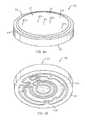
- FIG. 1is a schematic sectional side view of an embodiment of an electrostatic chuck
- FIG. 2is a schematic bottom view of the chuck of FIG. 1 ;
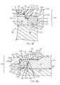
- FIG. 3is a schematic side view of an optical temperature sensor
- FIGS. 4A and 4Bare schematic perspective views of the top ( FIG. 4A ) and bottom ( FIG. 4B ) of an embodiment of a substrate support comprising a base and electrostatic chuck;
- FIG. 4Cis a schematic perspective top view of another embodiment of a substrate support comprising a base and electrostatic chuck;
- FIG. 4 C 1is perspective detailed view of circled section 4 C 1 of FIG. 4C , showing a peripheral zone with a peripheral port and surrounding sealing rims;
- FIG. 4Dis a bottom plan view of the base of the support of FIG. 4C ;
- FIG. 5Ais a schematic sectional side view of an embodiment of a ring assembly comprising an edge ring over a clamp ring on the substrate support of FIGS. 4A and 4B ;
- FIG. 5Bis a detailed view of the ring assembly of FIG. 5A ;
- FIG. 5Cis a schematic sectional side view of another embodiment of a ring assembly comprising an edge ring over a clamp ring on a substrate support;
- FIG. 6is schematic sectional side view of an embodiment of an electrical connector assembly of a base
- FIG. 7is schematic sectional side view of an embodiment of an contact band.
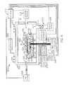
- FIG. 8is a schematic side view of an embodiment of a substrate processing chamber with the substrate support.
- An embodiment of an electrostatic chuck 20comprises a ceramic puck 24 comprising a ceramic body having a substrate receiving surface 26 that is the top surface of the puck 24 and which serves to hold a substrate 25 , as shown in FIG. 1 .
- the ceramic puck 24also has a backside surface 28 opposing the substrate receiving surface 26 .
- the ceramic puck 24further has a peripheral ledge 29 having a first step 31 and a second step 33 , the second step 33 being radially outward from, and lower than, the first step 31 .
- the ceramic puck 24comprises at least one of aluminum oxide, aluminum nitride, silicon oxide, silicon carbide, silicon nitride, titanium oxide, zirconium oxide, and mixtures thereof.
- the ceramic puck 24can be unitary monolith of ceramic made by hot pressing and sintering a ceramic powder, and then machining the sintered form to form the final shape of the puck 24 .
- the backside surface 28 of the ceramic puck 24comprises a plurality of spaced apart mesas 30 which are each cylindrical mounds that are separated from each other by a plurality of gaps 32 .
- the gaps 32are filled with a gas, such as air, to regulate the heat transfer rates from the backside surface 28 to other underlying surfaces of other structures.
- the mesas 30comprise cylindrical mounds, which can even be shaped as posts, that extend up from the surface 28 , the posts having a rectangular or circular cross-sectional shape.
- the height of the mesas 30can be from about 10 to about 50 microns, and the width (or diameter) of the mesas 30 from about 500 to about 5000 microns.
- the mesas 30can also have other shapes and sizes, for example, cones or rectangular blocks, or even bumps of varying sizes.
- the mesas 30are formed by bead blasting the backside surface 28 with a bead size that is suitably small, for example, in the tens of microns, to etch away by erosion the material of the backside surface 28 to form the shaped mesas 30 with the intervening gaps 32 .
- the ceramic puck 24also comprises an electrode 36 embedded therein to generate an electrostatic force to retain a substrate placed on the substrate receiving surface 26 .
- the electrode 36is a conductor, such as a metal, and be shaped as a monopolar or bipolar electrode.
- Monopolar electrodescomprise a single conductor and have a single electrical connection to an external electrical power source and cooperate with the charged species of the overlying plasma formed in a chamber to apply an electrical bias across the substrate held on the chuck 20 .
- Bipolar electrodeshave two or more conductors, each of which is biased relative to the other to generate an electrostatic force to hold a substrate.
- the electrode 36can be shaped as a wire mesh or a metal plate with suitable cut-out regions.
- an electrode 36 comprising a monopolar electrodecan be a single continuous wire mesh embedded in the ceramic puck as shown.
- An embodiment of an electrode 36 comprising a bipolar electrodecan be a pair of filled-in C-shaped plates that face one another across the straight leg of the C-shape.
- the electrode 36can be composed of aluminum, copper, iron, molybdenum, titanium, tungsten, or alloys thereof.
- One version of the electrode 36comprises a mesh of molybdenum.
- the electrode 36is connected to a terminal post 58 which supplies electrical power to the electrode 36 from an external power supply.
- the ceramic puck 24also has a plurality of heat transfer gas conduits 38 a,b that traverse the ceramic body and terminating in ports 40 a,b on the substrate receiving surface 26 to provide heat transfer gas to the substrate receiving surface 26 .
- the heat transfer gaswhich can be for example, helium, is supplied below the substrate backside 34 to conduct heat away from the overlying substrate 25 and to the receiving surface 26 of the ceramic puck 24 .
- a first gas conduit 38 acan be located to supply heat transfer gas to a central heating zone 42 a of the substrate receiving surface 26
- a second gas conduit 38 bcan be located to supply heat transfer gas to a peripheral heating zone 42 b of the substrate receiving surface 26 .
- the central and peripheral heating zones 42 a,b of the substrate receiving surface 26 of the ceramic puck 24allow corresponding portions of the substrate process surface 44 , for example, the overlying central and peripheral portions 46 a,b of the substrate 25 , respectively, to be maintained at different temperatures.
- the temperatures at the central and peripheral heating zones 42 a,b of the substrate receiving surface 26 of the ceramic puck 24are further controlled using a plurality of heater coils 50 , 52 , for example, a first heater coil 50 and a second heater coil 52 , embedded in the ceramic puck 24 .
- the heater coils 50 , 52can be radially spaced apart and concentric about one another, and even side by side and in the same plane.
- the first heater coil 50is located at a central portion 54 a of the ceramic puck 24 and the second heater coil 52 located at a peripheral portion 54 b of the ceramic puck 24 .
- the first and second heater coils 50 , 52allow independent control of the temperatures of the central and peripheral portions 54 a , 54 b of the ceramic puck 24 , and further cooperate with the mesas 30 on the backside surface 28 of the ceramic puck 24 to allow regulation of a temperature profile of a substrate 25 placed on the receiving surface 26 of the ceramic puck 24 .
- Each heater coil 50 , 52provides the ability to independently control the temperatures of the heating zones 42 a,b , to achieve different processing rates or characteristics across the radial direction of the processing surface 44 of the substrate 25 . As such, different temperatures can be maintained at the two heating zones 42 a,b to affect the temperatures of the overlying central and peripheral portions 46 a,b of the substrate 25 , thereby counteracting any variable gas species distribution or heat load occurring during processing of the substrate 25 .
- the temperature of the peripheral heating zone 42 bis elevated to a higher temperature than the central heating zone 42 a to provide a more uniform processing rates or process characteristics across the processing surface 44 of the substrate 25 .
- the first and second heater coils 50 , 52each comprise circular loops of resistive heating elements that are arranged side by side, and can even be substantially in the same plane.
- the heater coils 50 , 52can each be a continuous concentric loop that gradually spirals radially inward in the body of the ceramic puck 24 .
- the heater coils 50 , 52can also be spiral coils that spiral about an axis passing through the center of the coils, for example, like a light bulb filament, which are positioned in concentric circles across the inside volume of the ceramic puck 24 .
- the resistive heating elementscan be composed of different electrically resistive materials, such as for example, molybdenum.
- the heater coils 50 , 52each comprise an electrical resistance sufficiently high to maintain the substrate receiving surface 26 of the ceramic puck 24 at temperatures of from about 80 to about 250° C.
- the electrical resistance of the coilsare from about 4 to about 12 Ohms.
- the first heater coil 50has an electrical resistance of 6.5 ohm and the second heater coil 52 has an electrical resistance inner of 8.5 ohm.
- the heater coils 50 , 52are powered via independent terminal posts 58 a - d which extend through the ceramic puck 24 .
- the pressure of heat transfer gascan also be controlled in the two zones 42 a,b to render the substrate processing rates more uniform across the substrate 25 .
- the two zones 42 a,bcan each be set to hold heat transfer gas at a different equilibrated pressure to provide different heat transfer rates from the backside 34 of the substrate 25 . This is accomplished by supplying heat transfer gas at two different pressures through the two conduits 38 a , 38 b , respectively, to exit at two different locations of the substrate receiving surface 26 .
- the electrostatic chuck 20can also include optical temperature sensors 60 a,b that pass through holes 62 a,b in the ceramic puck 24 to contact and accurately measure the temperatures of the overlying central and peripheral portions 46 a,b of the substrate 25 .
- a first sensor 60 ais positioned at the central heating zone 42 a of the ceramic puck 24 to read the temperature of the central portion 46 a of the substrate 25
- a second sensor 60 bis positioned at the peripheral heating zone 42 b of the ceramic puck 24 to correspondingly read the temperature at the peripheral portion 46 b of the substrate 25 .
- the optical temperature sensors 60 a,bare positioned in the chuck 20 so that the tips 64 a,b of the sensors lies in a plane with the substrate receiving surface 26 of the ceramic puck 24 , such that the sensor tips 64 a,b can contact the backside 34 of the substrate 25 held on the chuck 20 .
- the legs 66 a,b of the sensors 60 a,bextend vertically through the body of the ceramic puck 24 .
- each optical temperature sensor 60comprises a heat sensor probe 68 comprising a copper cap 70 shaped as a closed off cylinder with a side 72 and a dome-shaped top 74 that serves as the tip 64 .
- the copper cap 70can be composed of oxygen free copper material.
- a phosphorous plug 76is embedded inside, and in direct contact with, the top 74 of the copper cap 70 .
- the phosphorous plug 76 embedded in the copper cap 70provides quicker and more sensitive thermal response for the heat sensing probe 68 .
- the tip 64 of the copper cap 70is a dome-shaped top 74 to allow repeated contact with different substrates 25 without eroding or damaging the substrates.
- the copper cap 70has a recessed groove 78 for receiving epoxy 79 to affix the cap 70 in the sensor probe 68 .
- the phosphorous plug 76converts heat in the form of infrared radiation to photons which are passed though an optical fiber bundle 80 .
- the optical fiber bundle 80can be composed of borosilicate glass fibers.
- the optical fiber bundle 80is encased by a sleeve 82 , which in turn is partially surrounded by a temperature isolation jacket 84 that serves to isolate the temperature sensor from the heat of the base that supports the ceramic puck.
- the sleeve 82can be a glass tubing to provide better thermal insulation from the surrounding structure, but can also be made from a metal such as copper.
- the temperature isolation jacket 84may be composed of PEEK, a polyetheretherketone, and can also be Teflon® (polytetrafluoroethylene) from Dupont de Nemours Co. Delaware.
- a substrate support 90comprises the electrostatic chuck 20 secured to a base 91 which is used to support and secure the chuck 20 , as shown in FIGS. 4A , 4 B and 5 A.
- the base 91comprises a metal body 92 with a top surface 94 having a chuck receiving portion 96 and peripheral portion 98 .
- the chuck receiving portion 96 of the top surface 94is adapted to receive the backside surface 28 of the ceramic puck 24 of the electrostatic chuck 20 .
- the peripheral portion 98 of the base 91extends radially outward beyond the ceramic puck 24 .
- the peripheral portion 98 of the base 91can be adapted to receive a clamp ring 100 which can be secured to the top surface of the peripheral portion of the base.
- the metal body 92 of the base 91has a number of passages 102 running from a bottom surface 104 of the base to the top surface 94 of the base 91 , to for example, hold the terminals 58 a - d or feed gas to the gas conduits 38 a,b of the ceramic puck 24 .
- the chuck receiving portion 96 of the top surface 94 of the base 91comprises one or more grooves 106 a,b to retain and flow air across the backside of the ceramic puck 24 .
- the chuck receiving portion 96comprises a peripheral groove 106 a which cooperates with a plurality of mesas 30 on the backside surface 28 of a ceramic puck 24 to control a rate of heat transfer from the peripheral portion 54 b of the ceramic puck 24 .
- a central groove 106 bis used in conjunction with the peripheral groove 106 a to regulate heat transfer from the central portion 54 a of the ceramic puck 24 .
- the grooves 106 a,b in the top surface 94 of the base 91cooperate with the mesas 30 on the backside surface 28 of the ceramic puck 24 to further regulate the temperatures across the substrate processing surface 44 .
- the shape, size, and spacing of the mesas 30control the total amount of contact surface of the mesas 30 with the top surface 94 of the base 91 thereby controlling the total heat conduction area of the interface.
- the mesas 30can be shaped and sized so that only 50% or less, for example 30%, of the total area of the backside surface 28 of the ceramic puck 24 actually contacts the top surface 94 of the base 91 . The less the contact area, the higher the temperatures across the substrate processing surface 44 .
- airis provided between the mesas 30 and across the backside surface 28 to serve as a further temperature regulator.
- the mesas 30 on the backside surface 28 of the ceramic puck 24can be distributed across the backside surface 28 in a uniform or non-uniform pattern. In a uniform pattern, the distance between the mesas 30 as represented by the gaps 32 remain substantially the same, and in a non-uniform spacing the gaps distance varies across the surface 28 .
- the shape and size of the mesas 30can also be made to vary across the surface 28 .
- a non-uniform pattern of mesas 30can be arranged to provide different amounts of contact surface across the backside surface 28 of the ceramic puck 24 at different regions, to control the heat transfer rates from the central and peripheral portions 54 a,b , respectively, of the puck 24 , and thus, the temperatures at the central and peripheral portions 46 a,b of the overlying substrate 25 .
- the base 91further comprises a plurality of channels 110 for circulating a fluid, such as water.
- the base 91 with the circulating cooling fluidserves as a heat exchanger to control the temperatures of the chuck 20 to achieve desired temperatures across the processing surface 44 of the substrate 25 .
- the fluid passed through the channels 110can be heated or cooled to raise or lower the temperature of the chuck 20 and that of the substrate 25 held on the chuck 20 .
- the channels 110are shaped and sized to allow fluid to flow through to maintain the base 91 at temperatures of from about 0 to 120° C.
- the base 91further comprises an electrical terminal assembly for conducting electrical power to the electrode 36 of the electrostatic chuck 20 .
- the electrical terminal assemblycomprises a ceramic insulator jacket 124 .
- the ceramic insulator jacket 124can be for example, aluminum oxide.
- a plurality of terminal posts 58are embedded within the ceramic insulator jacket 124 .
- the terminal posts 58 , 58 a - dsupply electrical power to the electrode 36 and heater coils 50 , 52 of the electrostatic chuck 20 .
- the terminal posts 58can include copper posts.
- the contact bands 140are configured to surround the terminal posts 58 , 58 a - d , of the electrical terminal assembly, as shown in FIG. 7 .
- Each contact band 140comprises metal, such as, for example, a copper alloy.
- the structural body of the contact band 140comprises a casing 142 adapted to fit around a terminal post 58 .
- the shape of the casing 142is dependent upon the shape of the post 58 and optimally, should mimic the shape of the post 58 .
- a portion or a strip 146 of the casing 142comprises a band 144 with a plurality of slots 148 and a plurality of heat transfer louvers 150 ; the slots 148 configured in a pattern to consequently create the louvers 150 alternating with the slots 148 .
- the plurality of slots 148 and louvers 150extend from a top edge 152 of the strip 146 to the bottom edge 154 of the strip 146 or a portion of the casing 142 .
- the plurality of slots 148 and louvers 150create a spring-like characteristic reducing the stiffness of the casing 142 and allowing it to conform around the outside surface of the terminal post 58 or terminal.
- the configuration of the plurality of slots 148 on the strip 146 of the casing 142also, through its spring-like characteristics, causes the terminal post 58 to be in contact with substantial regions of the inner exposed surfaces 143 of the casing 142 . This allows for optimal heat transfer between the contact band 140 and the terminal.
- a ring assembly 170can also be provide to reduce the formation of process deposits on, and protect from erosion, peripheral regions of the substrate support 90 comprising the electrostatic chuck 20 supported by the base 91 , as shown in FIG. 5A .
- the ring assembly 170comprises a clamp ring 100 comprising an annular body 171 having holes 175 that are secured to the peripheral portion 98 of the top surface 94 of the base 91 with securing means such as screws or bolts 169 .
- the clamp ring 100has an upper lip 172 which extends radially inward from a top surface 174 and an outer side surface 176 which forms the radially outer perimeter of the clamp ring 100 .
- the lip 172has an undersurface 173 which is sized to fit and rest on the first step 31 of the peripheral ledge 29 of the ceramic puck 24 .
- the lip 172has an undersurface 173 which is adapted to form a gas-tight seal between the ceramic puck 24 and the base 91 .
- the undersurface 173can comprise a polymer, such as a polymer layer, for example polyimide, to form a good seal.
- the clamp ring 100is fabricated from a material that can resist erosion by plasma, for example, a metallic material such as stainless steel, titanium or aluminum; or a ceramic material, such as aluminum oxide.
- the ring assembly 170also includes an edge ring 180 comprising a band 182 having a foot 184 which rests on the top surface 174 of the clamp ring 100 as shown in FIG. 5B .
- the edge ring 180also has an annular outer wall 186 enclosing the outer side surface 176 of the clamp ring 100 which would otherwise be exposed to the processing environment to reduce or prevent deposition of sputtering deposits on the clamp ring 100 .
- the edge ring 180also has a flange 190 covering the second step 33 of the peripheral ledge 29 of the ceramic puck 24 .
- the flange 190comprises a projection 194 that terminates below an overhanging edge 196 of the substrate 25 .
- the flange 190defines an inner perimeter of the edge ring 180 that surrounds the periphery of the substrate 25 to protect regions of the ceramic puck 24 that are not covered by the substrate 25 during processing.
- the clamp ring 100 and the edge ring 180 of the ring assembly 170cooperate to reduce the formation of process deposits on, and protect from erosion, the electrostatic chuck 20 supported on the base 91 during the processing of a substrate 25 .
- the edge ring 180also protects the exposed side surfaces of the substrate support 90 to reduce erosion in the process.
- the ring assembly 170can be easily removed to clean deposits from the exposed surfaces of the clamp ring 100 , and edge ring 180 , so that the entire substrate support 90 does not have to be dismantled to be cleaned.
- the edge ring 180can be made from a ceramic, such as for example, quartz.
- the clamp ring 100comprises an annular body 171 having a top surface 174 for supporting an edge ring 180 and a bottom surface 192 with a plurality of holes 175 adapted to be secured to the peripheral portion 98 of the top surface 94 of the base 91 .
- the annular body 171is secured to the peripheral portion 98 of the top surface 94 of the base 91 by screws or bolts 169 that mate with the holes 175 .
- the clamp ring 100also has an upper lip 172 that extends radially inward to rest on the first step 31 of the peripheral ledge 29 of the ceramic puck 24 .
- the upper lip 172 of the clamp ring 100can also have a downwardly projecting bump 192 that rests on the first step 31 of the peripheral ledge 29 of the ceramic puck 24 to minimize contact area, and downwardly projecting bump 193 extending out from a radially outward bottom recess 194 .
- the upper lip 172 of the clamp ring 100comprises an undersurface 173 which rests on the first step 31 of the peripheral ledge 29 of the ceramic puck 24 , and this undersurface 173 comprises, in one version, a polymer, such as a layer of polymer, for example, a polyimide.
- the undersurface 173can also be the surface of the bump 193 , for example, the bump 193 can be made of the undersurface material.
- the outer portion 194 of the clamp ring 100comprises a radially outer side surface 176 which is flat and terminates at an outer diameter 196 of the base 91 .
- the clamp ring 100also has a foot 197 which extends downward from the radially outer side surface 176 to rest on the peripheral portion 98 of the top surface 94 of the base 91 .
- the clamp ring 100can be made from a metal such as aluminum, titanium or stainless steel; or a ceramic, such as aluminum oxide.
- the version of the edge ring 180 shown in FIG. 5Ccomprises a band 182 which is wedge-shaped with an inclined upper surface 183 .
- a lower surface 185 of the band 182covers the top surface 174 of the clamp ring 100 .
- the edge ring 180also has an inner flange 187 that extends radially inward from the wedge-shaped band 182 .
- the inner flange 187comprises a bottom surface 188 that is stepped up in relation to the lower surface 185 of wedge-shaped band 182 .
- the inner flange 187also has a foot 189 that can rest on the first step 33 of the peripheral ledge 29 of the ceramic puck 24 .
- the inner flange 187further comprises an upper surface 191 which has a radially inward perimeter comprising an upper step 232 and a lower step 234 .
- the upper and lower steps 232 , 234step down in height along the radially inward direction.
- the inner flange 187also has a curved edge 236 that joins to the inclined upper surface 183 of the wedge-shaped band 182 .
- An outer flange 238 of the edge ring 180extends radially outward from the wedge-shaped band 182 .
- the outer flange 238comprises a radially inward facing surface 240 that covers the outer side surface 176 of the clamp ring 100 .
- the outer flange 238further has a bottom wall 242 that extends downwardly in relation to the lower surface 185 of wedge-shaped band 182 .
- the outer flange 238also has a slanted perimeter edge 244 which reduces erosion of this region.
- the edge ring 180can also be made from a ceramic, such as quartz.
- the electrostatic chuck 20comprises a ceramic puck 24 with a substrate receiving surface 26 , as shown in FIGS. 4 C and 4 C 1 .
- the substrate receiving surface 26comprises a pattern of grooves 250 comprising radial arms 252 and circular arms 254 which are interconnected to one another.
- raised plateaus 256In between these grooves 250 are raised plateaus 256 of spaced apart mesas 258 .
- the raised plateaus 256have an arcuate side edge 257 and are generally triangular or trapezoid shaped.
- the raised plateaus 256can also have other shapes and can be distributed across the substrate receiving surface 26 in a non-symmetrical pattern.
- Each raised plateau 256is defined by a plurality of mesas 258 that can, for example, number from about 10 to about 1000 mesas.
- the mesas 258are raised cylindrical bumps, for example, shaped as cylinders or arcuate projections.
- the mesas 258can be cylinders having average diameters of from about 5 to about 50 microns and heights of from about 0.5 to about 5 mm.
- the mesas 258are provided in a shape, size, and spatial distribution across the surface 26 to control the contact area with the overlying substrate to regulate heat transfer rates from the substrate to different regions of the ceramic puck 24 .
- a plurality of heat transfer gas conduits 38 a,btraverse through the ceramic puck 24 and terminate in one or more central ports 40 a and peripheral ports 40 b located in the pattern of grooves 250 on the substrate receiving surface 26 .
- the central and peripheral ports 40 a,bare capable of providing heat transfer gas to a central zone 42 a and a peripheral zone 42 b , respectively, of the substrate receiving surface 26 .
- the peripheral ports 40 bterminate in the arcuate cut-outs 259 which are surrounded by a radially inner gas sealing rim 260 and a radially outer gas sealing rim 262 to define the peripheral zone 42 b .
- the central ports 40 acan terminate at intersections of the central arms 252 and radial arms 254 of the grooves 250 to define a region corresponding the central zone 42 a .
- the central and peripheral heating zones 42 a,b of the substrate receiving surface 26 of the ceramic puck 24allow corresponding overlying central and peripheral portions 46 a,b of the substrate 25 , respectively, to be maintained at different temperatures ( FIG. 8 ).
- the ceramic puck 24has a backside surface 28 (not shown) opposing the substrate receiving surface 26 which can be planar and absent mesas, or which can have mesas previously described.
- the ceramic puck 24also has a peripheral ledge 29 having a first step 31 and a second step 33 , the second step 33 being radially outward from, and lower than, the first step 31 .
- the ceramic puck 24is made from aluminum oxide, aluminum nitride, silicon oxide, silicon carbide, silicon nitride, titanium oxide, zirconium oxide, or mixtures thereof; by hot pressing and sintering a ceramic powder and machining the sintered ceramic form to form the final shape of the puck 24 .
- the grooves 250 , mesas 258 , gas conduits 38 a,b and ports 40 a,b , and other structuresare machined into the ceramic structure.
- the base 91comprises a metal body 92 with a top surface 94 (not shown) having a chuck receiving portion 96 and a peripheral portion 98 which extends radially outward beyond the ceramic puck 24 .
- the base 91comprises a single channel 110 for circulating a fluid, such as water, to serve as a heat exchanger.
- the fluid circulating channel 110comprises a serpentine channel which has a plurality of curved hump regions 260 a - c which are distributed non-uniformly or asymmetrically across the base 91 .
- a greater length of the channel 110is provide to pass through or across those regions of the base 91 which get hotter in use, and a shorter length is used at the cooler regions of the base 91 .
- the resultant asymmetric fluid circulating channel 110controls the fluid flow to maintain uniform temperatures across the base 91 .
- the substrate support 90comprising the electrostatic chuck 20 and the base 91 , can be used in a substrate processing apparatus 200 , and exemplary version of which is illustrated in FIG. 8 .
- the apparatus 200comprises a chamber 201 comprising enclosing walls 202 , and in one version, the chamber 201 is a DPS Advantage Chamber.
- a gas source 204provides a process gas to the chamber through gas holes 203 , the process gas being capable of processing the substrate 25 , such as an etching gas, for example, a halogen-containing gas such as chlorine or hydrogen chloride; or a deposition gas, such as a CVD or PVD gas, for example, a gas for depositing dielectric or semiconducting materials.
- a gas energizer 208is provided to capacitively or inductively couple RF energy to the process gas respectively, or transmit microwave energy into the process gas (not shown), to form an energized gas to process the substrate 25 .
- the process gascan be energized capacitively by applying an RF voltage to the electrode 36 of the electrostatic chuck 20 via an electrode power supply 230 and electrically grounding a wall 202 of the chamber 201 .
- the electrode power supply 230also provides a DC chucking voltage to charge the electrode 36 of the chuck 20 to electrostatically hold the substrate 25 .
- the process gascan also be energized by coupling inductive energy to the process gas via the inductor coil 205 .
- the process gascan be energized by coupling microwave energy to the process gas via a microwave conduit in a remote chamber (not shown).
- the substrate 25is held in the chamber 201 on a receiving surface 26 of the electrostatic chuck 20 , which in turn rests on the base 91 .
- the chamberis controlled by a controller 212 which typically comprises as a computer having a central processing unit (CPU), such as a Pentium processor commercially available from Intel Corporation, Santa Clara, Calif., coupled to a memory and peripheral computer components.
- the memorymay include a removable storage, such as a CD or floppy drive; a non-removable storage, such as a hard drive; and random access memory (RAM).
- the controller 212may further comprise a hardware interface comprising analog or digital input and output boards, and motor controller boards.
- An operatorcan communicate with the chamber controller 212 via a display or data input device. To select a particular screen or function, the operator enters the selection using the data input device, such as a keyboard or light pen.
- the controller 212also comprises a computer-readable program stored in the memory, comprising program code capable of controlling and monitoring the processes conducted in the chamber 201 .
- the computer-readable programmay be written in any conventional computer-readable programming language. Suitable program code is entered into single or multiple files using a conventional text editor and stored or embodied in computer-usable medium of the memory. If the entered code text is in a high level language, the code is compiled, and the resultant compiler code is then linked with an object code of pre-compiled library routines. To execute the linked, compiled object code, the user invokes the object code, causing the CPU to read and execute the code to perform the tasks identified in the program.
- the programcan include a temperature control instruction set to control the temperatures at different regions of the substrate 25 , by for example, independently applying different electrical power levels to the fist and second heater coils 50 , 52 in the ceramic puck 24 of the chuck 20 , adjust the flow of heat transfer gas through the conduits 38 a,b and controlling the flow rate of fluid through the channels 110 of the base 91 .
- a process feedback control instruction setcan serve as a feedback control loop between a temperature monitoring instruction set which receives temperature signals from the optical temperature sensors 60 a,b to adjust the power applied to the chamber components, such as the heater coils 50 , 52 , flow of heat transfer gas through the conduits 38 a,b , and flow of fluid through the channels 110 of the base 91 .
- each of these instruction setscan be integrated with one another or may be over-lapping; thus, the chamber controller 212 and the computer-readable program described herein should not be limited to the specific version of the functional routines described herein.
Landscapes
- Engineering & Computer Science (AREA)
- Physics & Mathematics (AREA)
- Condensed Matter Physics & Semiconductors (AREA)
- General Physics & Mathematics (AREA)
- Manufacturing & Machinery (AREA)
- Computer Hardware Design (AREA)
- Microelectronics & Electronic Packaging (AREA)
- Power Engineering (AREA)
- Container, Conveyance, Adherence, Positioning, Of Wafer (AREA)
Abstract
Description
Claims (34)
Priority Applications (2)
| Application Number | Priority Date | Filing Date | Title |
|---|---|---|---|
| US11/740,869US8226769B2 (en) | 2006-04-27 | 2007-04-26 | Substrate support with electrostatic chuck having dual temperature zones |
| US13/556,156US8663391B2 (en) | 2006-04-27 | 2012-07-23 | Electrostatic chuck having a plurality of heater coils |
Applications Claiming Priority (2)
| Application Number | Priority Date | Filing Date | Title |
|---|---|---|---|
| US79601306P | 2006-04-27 | 2006-04-27 | |
| US11/740,869US8226769B2 (en) | 2006-04-27 | 2007-04-26 | Substrate support with electrostatic chuck having dual temperature zones |
Related Child Applications (1)
| Application Number | Title | Priority Date | Filing Date |
|---|---|---|---|
| US13/556,156ContinuationUS8663391B2 (en) | 2006-04-27 | 2012-07-23 | Electrostatic chuck having a plurality of heater coils |
Publications (2)
| Publication Number | Publication Date |
|---|---|
| US20070258186A1 US20070258186A1 (en) | 2007-11-08 |
| US8226769B2true US8226769B2 (en) | 2012-07-24 |
Family
ID=38660961
Family Applications (2)
| Application Number | Title | Priority Date | Filing Date |
|---|---|---|---|
| US11/740,869Expired - Fee RelatedUS8226769B2 (en) | 2006-04-27 | 2007-04-26 | Substrate support with electrostatic chuck having dual temperature zones |
| US13/556,156ActiveUS8663391B2 (en) | 2006-04-27 | 2012-07-23 | Electrostatic chuck having a plurality of heater coils |
Family Applications After (1)
| Application Number | Title | Priority Date | Filing Date |
|---|---|---|---|
| US13/556,156ActiveUS8663391B2 (en) | 2006-04-27 | 2012-07-23 | Electrostatic chuck having a plurality of heater coils |
Country Status (1)
| Country | Link |
|---|---|
| US (2) | US8226769B2 (en) |
Cited By (47)
| Publication number | Priority date | Publication date | Assignee | Title |
|---|---|---|---|---|
| US20100043709A1 (en)* | 2006-11-02 | 2010-02-25 | Pyung-Yong Um | Chemical vapor deposition apparatus for equalizing heating temperature |
| US20100319855A1 (en)* | 2008-02-04 | 2010-12-23 | Eugene Technology Co., Ltd. | Substrate supporting unit, substrate processing apparatus, and method of manufacturing substrate supporting unit |
| US20110154843A1 (en)* | 2009-12-31 | 2011-06-30 | Ko Sungyong | Apparatus for controlling temperature of electrostatic chuck comprising two-stage refrigerant fluid channel |
| US20110186545A1 (en)* | 2010-01-29 | 2011-08-04 | Applied Materials, Inc. | Feedforward temperature control for plasma processing apparatus |
| US20120132397A1 (en)* | 2010-06-08 | 2012-05-31 | Applied Materials, Inc. | Temperature control in plasma processing apparatus using pulsed heat transfer fluid flow |
| US20130174983A1 (en)* | 2001-07-10 | 2013-07-11 | Tokyo Electron Limited | Plasma processor and plasma processing method |
| US8663391B2 (en)* | 2006-04-27 | 2014-03-04 | Applied Materials, Inc. | Electrostatic chuck having a plurality of heater coils |
| US20140151360A1 (en)* | 2012-11-30 | 2014-06-05 | Wd Media, Inc. | Heater assembly for disk processing system |
| US20140204975A1 (en)* | 2011-08-26 | 2014-07-24 | Sumitomo Osaka Cement Co., Ltd. | Plate-shaped body for temperature measurement and temperature measuring apparatus provided with the same |
| US20150201468A1 (en)* | 2012-09-27 | 2015-07-16 | Tokyo Electron Limited | Heat Treatment Apparatus |
| US9089007B2 (en) | 2012-04-27 | 2015-07-21 | Applied Materials, Inc. | Method and apparatus for substrate support with multi-zone heating |
| US20150206723A1 (en)* | 2014-01-17 | 2015-07-23 | Psk Inc. | Support unit and apparatus for treating substrate |
| US20150288302A1 (en)* | 2012-11-27 | 2015-10-08 | Creative Technology Corporation | Electrostatic chuck, glass substrate processing method, and said glass substrate |
| US20150368829A1 (en)* | 2014-06-23 | 2015-12-24 | Applied Materials, Inc. | Substrate thermal control in an epi chamber |
| US20160007411A1 (en)* | 2014-07-02 | 2016-01-07 | Applied Materials, Inc. | Temperature control apparatus including groove-routed optical fiber heating, substrate temperature control systems, electronic device processing systems, and processing methods |
| US9472435B2 (en) | 2014-07-23 | 2016-10-18 | Applied Materials, Inc. | Tunable temperature controlled substrate support assembly |
| US9472410B2 (en) | 2014-03-05 | 2016-10-18 | Applied Materials, Inc. | Pixelated capacitance controlled ESC |
| US9520315B2 (en) | 2013-12-31 | 2016-12-13 | Applied Materials, Inc. | Electrostatic chuck with internal flow adjustments for improved temperature distribution |
| US9622375B2 (en) | 2013-12-31 | 2017-04-11 | Applied Materials, Inc. | Electrostatic chuck with external flow adjustments for improved temperature distribution |
| US9639097B2 (en) | 2010-05-27 | 2017-05-02 | Applied Materials, Inc. | Component temperature control by coolant flow control and heater duty cycle control |
| US9681497B2 (en) | 2013-03-12 | 2017-06-13 | Applied Materials, Inc. | Multi zone heating and cooling ESC for plasma process chamber |
| US9698041B2 (en) | 2014-06-09 | 2017-07-04 | Applied Materials, Inc. | Substrate temperature control apparatus including optical fiber heating, substrate temperature control systems, electronic device processing systems, and methods |
| US9883549B2 (en) | 2006-07-20 | 2018-01-30 | Applied Materials, Inc. | Substrate support assembly having rapid temperature control |
| US20180261486A1 (en)* | 2014-12-10 | 2018-09-13 | Toto Ltd. | Electrostatic chuck and wafer processing apparatus |
| US10274270B2 (en) | 2011-10-27 | 2019-04-30 | Applied Materials, Inc. | Dual zone common catch heat exchanger/chiller |
| US10332772B2 (en) | 2013-03-13 | 2019-06-25 | Applied Materials, Inc. | Multi-zone heated ESC with independent edge zones |
| US10403534B2 (en) | 2013-11-11 | 2019-09-03 | Applied Materials, Inc. | Pixilated cooling, temperature controlled substrate support assembly |
| US10460968B2 (en) | 2013-12-02 | 2019-10-29 | Applied Materials, Inc. | Electrostatic chuck with variable pixelated magnetic field |
| US10622228B2 (en) | 2008-02-04 | 2020-04-14 | Eugene Technology Co., Ltd. | Substrate supporting unit, substrate processing apparatus, and method of manufacturing substrate supporting unit |
| US10654147B2 (en) | 2017-10-17 | 2020-05-19 | Applied Materials, Inc. | Polishing of electrostatic substrate support geometries |
| US20200161080A1 (en)* | 2018-11-16 | 2020-05-21 | Emcrafts Co., Ltd. | Electron microscope specimen mount |
| US10685861B2 (en) | 2016-08-26 | 2020-06-16 | Applied Materials, Inc. | Direct optical heating of substrates through optical guide |
| US10736182B2 (en) | 2014-07-02 | 2020-08-04 | Applied Materials, Inc. | Apparatus, systems, and methods for temperature control of substrates using embedded fiber optics and epoxy optical diffusers |
| US10793772B1 (en) | 2020-03-13 | 2020-10-06 | Accelovant Technologies Corporation | Monolithic phosphor composite for sensing systems |
| US20210087689A1 (en)* | 2019-09-19 | 2021-03-25 | Applied Materials, Inc. | Apparatus and Methods for Motor Shaft and Heater Leveling |
| US10973088B2 (en) | 2016-04-18 | 2021-04-06 | Applied Materials, Inc. | Optically heated substrate support assembly with removable optical fibers |
| US20210101249A1 (en)* | 2015-12-10 | 2021-04-08 | Ioneer, LLC. | Apparatus and method for determining parameters of process operation |
| US11158526B2 (en) | 2014-02-07 | 2021-10-26 | Applied Materials, Inc. | Temperature controlled substrate support assembly |
| US11353369B2 (en) | 2020-11-05 | 2022-06-07 | Accelovant Technologies Corporation | Optoelectronic transducer module for thermographic temperature measurements |
| US11359976B2 (en) | 2020-10-23 | 2022-06-14 | Accelovant Technologies Corporation | Multipoint surface temperature measurement system and method thereof |
| US11417557B2 (en) | 2020-12-15 | 2022-08-16 | Entegris, Inc. | Spiraling polyphase electrodes for electrostatic chuck |
| US11415538B2 (en) | 2020-03-06 | 2022-08-16 | Applied Materials, Inc. | Capacitive sensor housing for chamber condition monitoring |
| US20220301920A1 (en)* | 2020-07-27 | 2022-09-22 | Applied Materials, Inc. | Film thickness uniformity improvement using edge ring and bias electrode geometry |
| US11495440B2 (en) | 2017-04-07 | 2022-11-08 | Applied Materials, Inc. | Plasma density control on substrate edge |
| US11545346B2 (en) | 2020-03-06 | 2023-01-03 | Applied Materials, Inc. | Capacitive sensing data integration for plasma chamber condition monitoring |
| US11581206B2 (en) | 2020-03-06 | 2023-02-14 | Applied Materials, Inc. | Capacitive sensor for chamber condition monitoring |
| US12437979B2 (en) | 2020-03-06 | 2025-10-07 | Applied Materials, Inc. | Capacitive sensors and capacitive sensing locations for plasma chamber condition monitoring |
Families Citing this family (174)
| Publication number | Priority date | Publication date | Assignee | Title |
|---|---|---|---|---|
| US20060105182A1 (en)* | 2004-11-16 | 2006-05-18 | Applied Materials, Inc. | Erosion resistant textured chamber surface |
| US7221553B2 (en)* | 2003-04-22 | 2007-05-22 | Applied Materials, Inc. | Substrate support having heat transfer system |
| US7544251B2 (en) | 2004-10-07 | 2009-06-09 | Applied Materials, Inc. | Method and apparatus for controlling temperature of a substrate |
| US7436645B2 (en) | 2004-10-07 | 2008-10-14 | Applied Materials, Inc. | Method and apparatus for controlling temperature of a substrate |
| US7648914B2 (en) | 2004-10-07 | 2010-01-19 | Applied Materials, Inc. | Method for etching having a controlled distribution of process results |
| US20070091540A1 (en)* | 2005-10-20 | 2007-04-26 | Applied Materials, Inc. | Method of processing a workpiece in a plasma reactor using multiple zone feed forward thermal control |
| JP4831544B2 (en)* | 2006-08-29 | 2011-12-07 | エスアイアイ・ナノテクノロジー株式会社 | Thermal analyzer |
| US7649729B2 (en)* | 2007-10-12 | 2010-01-19 | Applied Materials, Inc. | Electrostatic chuck assembly |
| JP5222442B2 (en)* | 2008-02-06 | 2013-06-26 | 東京エレクトロン株式会社 | Substrate mounting table, substrate processing apparatus, and temperature control method for substrate to be processed |
| WO2009107718A1 (en)* | 2008-02-27 | 2009-09-03 | 東京エレクトロン株式会社 | Plasma etching apparatus and plasma etching method |
| TWI475594B (en) | 2008-05-19 | 2015-03-01 | Entegris Inc | Electrostatic chuck |
| WO2010021890A2 (en)* | 2008-08-19 | 2010-02-25 | Lam Research Corporation | Edge rings for electrostatic chucks |
| US8600543B2 (en)* | 2008-11-10 | 2013-12-03 | Kelk Ltd. | Apparatus and method for controlling temperature of semiconductor wafers |
| US20100116788A1 (en)* | 2008-11-12 | 2010-05-13 | Lam Research Corporation | Substrate temperature control by using liquid controlled multizone substrate support |
| WO2010090948A1 (en)* | 2009-02-04 | 2010-08-12 | Mattson Technology, Inc. | Electrostatic chuck system and process for radially tuning the temperature profile across the surface of a substrate |
| US8861170B2 (en) | 2009-05-15 | 2014-10-14 | Entegris, Inc. | Electrostatic chuck with photo-patternable soft protrusion contact surface |
| WO2010132640A2 (en) | 2009-05-15 | 2010-11-18 | Entegris, Inc. | Electrostatic chuck with polymer protrusions |
| US8270141B2 (en)* | 2009-11-20 | 2012-09-18 | Applied Materials, Inc. | Electrostatic chuck with reduced arcing |
| WO2011106625A1 (en)* | 2010-02-25 | 2011-09-01 | Stoneridge, Inc. | Soot sensor system |
| US9324576B2 (en) | 2010-05-27 | 2016-04-26 | Applied Materials, Inc. | Selective etch for silicon films |
| KR101731136B1 (en) | 2010-05-28 | 2017-04-27 | 엔테그리스, 아이엔씨. | High surface resistivity electrostatic chuck |
| US20110297088A1 (en)* | 2010-06-04 | 2011-12-08 | Texas Instruments Incorporated | Thin edge carrier ring |
| US9719169B2 (en)* | 2010-12-20 | 2017-08-01 | Novellus Systems, Inc. | System and apparatus for flowable deposition in semiconductor fabrication |
| US10283321B2 (en) | 2011-01-18 | 2019-05-07 | Applied Materials, Inc. | Semiconductor processing system and methods using capacitively coupled plasma |
| US9064815B2 (en) | 2011-03-14 | 2015-06-23 | Applied Materials, Inc. | Methods for etch of metal and metal-oxide films |
| US8999856B2 (en) | 2011-03-14 | 2015-04-07 | Applied Materials, Inc. | Methods for etch of sin films |
| CN103733076B (en) | 2011-05-26 | 2017-04-12 | 斯通瑞智公司 | Smoke sensor system |
| CN102856242B (en) | 2011-06-30 | 2016-06-08 | 细美事有限公司 | Substrate material support unit and the substrate material processing apparatus including it |
| JP5973731B2 (en)* | 2012-01-13 | 2016-08-23 | 東京エレクトロン株式会社 | Plasma processing apparatus and heater temperature control method |
| US9070536B2 (en)* | 2012-04-24 | 2015-06-30 | Applied Materials, Inc. | Plasma reactor electrostatic chuck with cooled process ring and heated workpiece support surface |
| US20130284372A1 (en)* | 2012-04-25 | 2013-10-31 | Hamid Tavassoli | Esc cooling base for large diameter subsrates |
| US9281226B2 (en)* | 2012-04-26 | 2016-03-08 | Applied Materials, Inc. | Electrostatic chuck having reduced power loss |
| US9490150B2 (en)* | 2012-07-03 | 2016-11-08 | Applied Materials, Inc. | Substrate support for substrate backside contamination control |
| JP5982206B2 (en)* | 2012-07-17 | 2016-08-31 | 東京エレクトロン株式会社 | Lower electrode and plasma processing apparatus |
| US9267739B2 (en) | 2012-07-18 | 2016-02-23 | Applied Materials, Inc. | Pedestal with multi-zone temperature control and multiple purge capabilities |
| US9373517B2 (en) | 2012-08-02 | 2016-06-21 | Applied Materials, Inc. | Semiconductor processing with DC assisted RF power for improved control |
| US9132436B2 (en) | 2012-09-21 | 2015-09-15 | Applied Materials, Inc. | Chemical control features in wafer process equipment |
| US10256079B2 (en) | 2013-02-08 | 2019-04-09 | Applied Materials, Inc. | Semiconductor processing systems having multiple plasma configurations |
| US9362130B2 (en) | 2013-03-01 | 2016-06-07 | Applied Materials, Inc. | Enhanced etching processes using remote plasma sources |
| US9040422B2 (en) | 2013-03-05 | 2015-05-26 | Applied Materials, Inc. | Selective titanium nitride removal |
| US20140251214A1 (en)* | 2013-03-06 | 2014-09-11 | Applied Materials, Inc. | Heated substrate support with flatness control |
| US20140271097A1 (en) | 2013-03-15 | 2014-09-18 | Applied Materials, Inc. | Processing systems and methods for halide scavenging |
| US9668373B2 (en) | 2013-03-15 | 2017-05-30 | Applied Materials, Inc. | Substrate support chuck cooling for deposition chamber |
| US9666466B2 (en)* | 2013-05-07 | 2017-05-30 | Applied Materials, Inc. | Electrostatic chuck having thermally isolated zones with minimal crosstalk |
| US9493879B2 (en) | 2013-07-12 | 2016-11-15 | Applied Materials, Inc. | Selective sputtering for pattern transfer |
| US9773648B2 (en) | 2013-08-30 | 2017-09-26 | Applied Materials, Inc. | Dual discharge modes operation for remote plasma |
| US9196514B2 (en)* | 2013-09-06 | 2015-11-24 | Applied Materials, Inc. | Electrostatic chuck with variable pixilated heating |
| WO2015043890A1 (en) | 2013-09-27 | 2015-04-02 | Asml Netherlands B.V. | Support table for a lithographic apparatus, lithographic apparatus and device manufacturing method |
| US9677177B2 (en) | 2013-10-24 | 2017-06-13 | Applied Materials, Inc. | Substrate support with quadrants |
| US9847222B2 (en) | 2013-10-25 | 2017-12-19 | Lam Research Corporation | Treatment for flowable dielectric deposition on substrate surfaces |
| US9576809B2 (en) | 2013-11-04 | 2017-02-21 | Applied Materials, Inc. | Etch suppression with germanium |
| US9520303B2 (en) | 2013-11-12 | 2016-12-13 | Applied Materials, Inc. | Aluminum selective etch |
| US9245762B2 (en) | 2013-12-02 | 2016-01-26 | Applied Materials, Inc. | Procedure for etch rate consistency |
| US9499898B2 (en) | 2014-03-03 | 2016-11-22 | Applied Materials, Inc. | Layered thin film heater and method of fabrication |
| US9299537B2 (en) | 2014-03-20 | 2016-03-29 | Applied Materials, Inc. | Radial waveguide systems and methods for post-match control of microwaves |
| US9903020B2 (en) | 2014-03-31 | 2018-02-27 | Applied Materials, Inc. | Generation of compact alumina passivation layers on aluminum plasma equipment components |
| WO2015153756A1 (en)* | 2014-04-01 | 2015-10-08 | Entegris, Inc. | Heated electrostatic chuck |
| US9309598B2 (en) | 2014-05-28 | 2016-04-12 | Applied Materials, Inc. | Oxide and metal removal |
| JP6378942B2 (en)* | 2014-06-12 | 2018-08-22 | 東京エレクトロン株式会社 | Mounting table and plasma processing apparatus |
| US9543171B2 (en)* | 2014-06-17 | 2017-01-10 | Lam Research Corporation | Auto-correction of malfunctioning thermal control element in a temperature control plate of a semiconductor substrate support assembly that includes deactivating the malfunctioning thermal control element and modifying a power level of at least one functioning thermal control element |
| US9496167B2 (en) | 2014-07-31 | 2016-11-15 | Applied Materials, Inc. | Integrated bit-line airgap formation and gate stack post clean |
| US9659753B2 (en) | 2014-08-07 | 2017-05-23 | Applied Materials, Inc. | Grooved insulator to reduce leakage current |
| US9553102B2 (en) | 2014-08-19 | 2017-01-24 | Applied Materials, Inc. | Tungsten separation |
| US10049921B2 (en) | 2014-08-20 | 2018-08-14 | Lam Research Corporation | Method for selectively sealing ultra low-k porous dielectric layer using flowable dielectric film formed from vapor phase dielectric precursor |
| US9355862B2 (en) | 2014-09-24 | 2016-05-31 | Applied Materials, Inc. | Fluorine-based hardmask removal |
| US9613822B2 (en) | 2014-09-25 | 2017-04-04 | Applied Materials, Inc. | Oxide etch selectivity enhancement |
| JP6463938B2 (en) | 2014-10-08 | 2019-02-06 | 日本特殊陶業株式会社 | Electrostatic chuck |
| US9355922B2 (en) | 2014-10-14 | 2016-05-31 | Applied Materials, Inc. | Systems and methods for internal surface conditioning in plasma processing equipment |
| US9966240B2 (en) | 2014-10-14 | 2018-05-08 | Applied Materials, Inc. | Systems and methods for internal surface conditioning assessment in plasma processing equipment |
| US11637002B2 (en) | 2014-11-26 | 2023-04-25 | Applied Materials, Inc. | Methods and systems to enhance process uniformity |
| US10573496B2 (en) | 2014-12-09 | 2020-02-25 | Applied Materials, Inc. | Direct outlet toroidal plasma source |
| US10224210B2 (en) | 2014-12-09 | 2019-03-05 | Applied Materials, Inc. | Plasma processing system with direct outlet toroidal plasma source |
| US10781518B2 (en) | 2014-12-11 | 2020-09-22 | Applied Materials, Inc. | Gas cooled electrostatic chuck (ESC) having a gas channel formed therein and coupled to a gas box on both ends of the gas channel |
| US9502258B2 (en) | 2014-12-23 | 2016-11-22 | Applied Materials, Inc. | Anisotropic gap etch |
| US9888528B2 (en) | 2014-12-31 | 2018-02-06 | Applied Materials, Inc. | Substrate support with multiple heating zones |
| US11257693B2 (en) | 2015-01-09 | 2022-02-22 | Applied Materials, Inc. | Methods and systems to improve pedestal temperature control |
| JP5962833B2 (en)* | 2015-01-16 | 2016-08-03 | Toto株式会社 | Electrostatic chuck |
| US20160225652A1 (en) | 2015-02-03 | 2016-08-04 | Applied Materials, Inc. | Low temperature chuck for plasma processing systems |
| US9728437B2 (en) | 2015-02-03 | 2017-08-08 | Applied Materials, Inc. | High temperature chuck for plasma processing systems |
| US9881805B2 (en) | 2015-03-02 | 2018-01-30 | Applied Materials, Inc. | Silicon selective removal |
| US10288361B2 (en)* | 2015-03-17 | 2019-05-14 | Hatco Corporation | Hot and cold shelf assembly with replaceable heating elements |
| US10186444B2 (en)* | 2015-03-20 | 2019-01-22 | Applied Materials, Inc. | Gas flow for condensation reduction with a substrate processing chuck |
| US9741593B2 (en) | 2015-08-06 | 2017-08-22 | Applied Materials, Inc. | Thermal management systems and methods for wafer processing systems |
| US9691645B2 (en) | 2015-08-06 | 2017-06-27 | Applied Materials, Inc. | Bolted wafer chuck thermal management systems and methods for wafer processing systems |
| US9349605B1 (en) | 2015-08-07 | 2016-05-24 | Applied Materials, Inc. | Oxide etch selectivity systems and methods |
| US10504700B2 (en) | 2015-08-27 | 2019-12-10 | Applied Materials, Inc. | Plasma etching systems and methods with secondary plasma injection |
| JP6614933B2 (en)* | 2015-11-11 | 2019-12-04 | 東京エレクトロン株式会社 | Substrate mounting mechanism and substrate processing apparatus |
| US9916977B2 (en) | 2015-11-16 | 2018-03-13 | Lam Research Corporation | Low k dielectric deposition via UV driven photopolymerization |
| US10388546B2 (en) | 2015-11-16 | 2019-08-20 | Lam Research Corporation | Apparatus for UV flowable dielectric |
| US10582570B2 (en)* | 2016-01-22 | 2020-03-03 | Applied Materials, Inc. | Sensor system for multi-zone electrostatic chuck |
| WO2017127163A1 (en)* | 2016-01-22 | 2017-07-27 | Applied Materials, Inc. | Ceramic showerhead with embedded conductive layers |
| JP6560150B2 (en)* | 2016-03-28 | 2019-08-14 | 日本碍子株式会社 | Wafer mounting device |
| US10504754B2 (en) | 2016-05-19 | 2019-12-10 | Applied Materials, Inc. | Systems and methods for improved semiconductor etching and component protection |
| US10522371B2 (en) | 2016-05-19 | 2019-12-31 | Applied Materials, Inc. | Systems and methods for improved semiconductor etching and component protection |
| US9865484B1 (en) | 2016-06-29 | 2018-01-09 | Applied Materials, Inc. | Selective etch using material modification and RF pulsing |
| US10062575B2 (en) | 2016-09-09 | 2018-08-28 | Applied Materials, Inc. | Poly directional etch by oxidation |
| US10629473B2 (en) | 2016-09-09 | 2020-04-21 | Applied Materials, Inc. | Footing removal for nitride spacer |
| JP6767833B2 (en)* | 2016-09-29 | 2020-10-14 | 日本特殊陶業株式会社 | Heating device |
| US10062585B2 (en) | 2016-10-04 | 2018-08-28 | Applied Materials, Inc. | Oxygen compatible plasma source |
| US10546729B2 (en) | 2016-10-04 | 2020-01-28 | Applied Materials, Inc. | Dual-channel showerhead with improved profile |
| US9721789B1 (en) | 2016-10-04 | 2017-08-01 | Applied Materials, Inc. | Saving ion-damaged spacers |
| US9934942B1 (en) | 2016-10-04 | 2018-04-03 | Applied Materials, Inc. | Chamber with flow-through source |
| US10062579B2 (en) | 2016-10-07 | 2018-08-28 | Applied Materials, Inc. | Selective SiN lateral recess |
| US9947549B1 (en) | 2016-10-10 | 2018-04-17 | Applied Materials, Inc. | Cobalt-containing material removal |
| US10163696B2 (en) | 2016-11-11 | 2018-12-25 | Applied Materials, Inc. | Selective cobalt removal for bottom up gapfill |
| US9768034B1 (en) | 2016-11-11 | 2017-09-19 | Applied Materials, Inc. | Removal methods for high aspect ratio structures |
| US10026621B2 (en) | 2016-11-14 | 2018-07-17 | Applied Materials, Inc. | SiN spacer profile patterning |
| US10242908B2 (en) | 2016-11-14 | 2019-03-26 | Applied Materials, Inc. | Airgap formation with damage-free copper |
| US10777442B2 (en)* | 2016-11-18 | 2020-09-15 | Applied Materials, Inc. | Hybrid substrate carrier |
| US10655224B2 (en)* | 2016-12-20 | 2020-05-19 | Lam Research Corporation | Conical wafer centering and holding device for semiconductor processing |
| CN110114853A (en)* | 2016-12-21 | 2019-08-09 | 应用材料公司 | It is deposited by the conformally sealed film of chemical vapor deposition |
| US10566206B2 (en) | 2016-12-27 | 2020-02-18 | Applied Materials, Inc. | Systems and methods for anisotropic material breakthrough |
| US10431429B2 (en) | 2017-02-03 | 2019-10-01 | Applied Materials, Inc. | Systems and methods for radial and azimuthal control of plasma uniformity |
| US10403507B2 (en) | 2017-02-03 | 2019-09-03 | Applied Materials, Inc. | Shaped etch profile with oxidation |
| US10043684B1 (en) | 2017-02-06 | 2018-08-07 | Applied Materials, Inc. | Self-limiting atomic thermal etching systems and methods |
| US10319739B2 (en) | 2017-02-08 | 2019-06-11 | Applied Materials, Inc. | Accommodating imperfectly aligned memory holes |
| US10943834B2 (en) | 2017-03-13 | 2021-03-09 | Applied Materials, Inc. | Replacement contact process |
| US10319649B2 (en) | 2017-04-11 | 2019-06-11 | Applied Materials, Inc. | Optical emission spectroscopy (OES) for remote plasma monitoring |
| JP7176860B6 (en) | 2017-05-17 | 2022-12-16 | アプライド マテリアルズ インコーポレイテッド | Semiconductor processing chamber to improve precursor flow |
| US11276559B2 (en) | 2017-05-17 | 2022-03-15 | Applied Materials, Inc. | Semiconductor processing chamber for multiple precursor flow |
| US11276590B2 (en) | 2017-05-17 | 2022-03-15 | Applied Materials, Inc. | Multi-zone semiconductor substrate supports |
| US10049891B1 (en) | 2017-05-31 | 2018-08-14 | Applied Materials, Inc. | Selective in situ cobalt residue removal |
| US10497579B2 (en) | 2017-05-31 | 2019-12-03 | Applied Materials, Inc. | Water-free etching methods |
| US10920320B2 (en) | 2017-06-16 | 2021-02-16 | Applied Materials, Inc. | Plasma health determination in semiconductor substrate processing reactors |
| US10541246B2 (en) | 2017-06-26 | 2020-01-21 | Applied Materials, Inc. | 3D flash memory cells which discourage cross-cell electrical tunneling |
| US10727080B2 (en) | 2017-07-07 | 2020-07-28 | Applied Materials, Inc. | Tantalum-containing material removal |
| US10541184B2 (en) | 2017-07-11 | 2020-01-21 | Applied Materials, Inc. | Optical emission spectroscopic techniques for monitoring etching |
| US10354889B2 (en) | 2017-07-17 | 2019-07-16 | Applied Materials, Inc. | Non-halogen etching of silicon-containing materials |
| US10170336B1 (en) | 2017-08-04 | 2019-01-01 | Applied Materials, Inc. | Methods for anisotropic control of selective silicon removal |
| US10043674B1 (en) | 2017-08-04 | 2018-08-07 | Applied Materials, Inc. | Germanium etching systems and methods |
| US10297458B2 (en) | 2017-08-07 | 2019-05-21 | Applied Materials, Inc. | Process window widening using coated parts in plasma etch processes |
| US10283324B1 (en) | 2017-10-24 | 2019-05-07 | Applied Materials, Inc. | Oxygen treatment for nitride etching |
| US10128086B1 (en) | 2017-10-24 | 2018-11-13 | Applied Materials, Inc. | Silicon pretreatment for nitride removal |
| KR102519544B1 (en)* | 2017-12-07 | 2023-04-07 | 삼성전자주식회사 | Wafer loading apparatus and film forming apparatus |
| US10256112B1 (en) | 2017-12-08 | 2019-04-09 | Applied Materials, Inc. | Selective tungsten removal |
| US10903054B2 (en) | 2017-12-19 | 2021-01-26 | Applied Materials, Inc. | Multi-zone gas distribution systems and methods |
| US11328909B2 (en) | 2017-12-22 | 2022-05-10 | Applied Materials, Inc. | Chamber conditioning and removal processes |
| US10854426B2 (en) | 2018-01-08 | 2020-12-01 | Applied Materials, Inc. | Metal recess for semiconductor structures |
| US11387134B2 (en)* | 2018-01-19 | 2022-07-12 | Applied Materials, Inc. | Process kit for a substrate support |
| US12293902B2 (en) | 2018-01-19 | 2025-05-06 | Applied Materials, Inc. | Process kit for a substrate support |
| US20190244787A1 (en)* | 2018-02-02 | 2019-08-08 | Wei-Chuan Chou | Plasma etching reaction chamber |
| US10679870B2 (en) | 2018-02-15 | 2020-06-09 | Applied Materials, Inc. | Semiconductor processing chamber multistage mixing apparatus |
| US10964512B2 (en) | 2018-02-15 | 2021-03-30 | Applied Materials, Inc. | Semiconductor processing chamber multistage mixing apparatus and methods |
| TWI766433B (en) | 2018-02-28 | 2022-06-01 | 美商應用材料股份有限公司 | Systems and methods to form airgaps |
| US10593560B2 (en) | 2018-03-01 | 2020-03-17 | Applied Materials, Inc. | Magnetic induction plasma source for semiconductor processes and equipment |
| US11515130B2 (en)* | 2018-03-05 | 2022-11-29 | Applied Materials, Inc. | Fast response pedestal assembly for selective preclean |
| US10319600B1 (en) | 2018-03-12 | 2019-06-11 | Applied Materials, Inc. | Thermal silicon etch |
| US10497573B2 (en) | 2018-03-13 | 2019-12-03 | Applied Materials, Inc. | Selective atomic layer etching of semiconductor materials |
| US10573527B2 (en) | 2018-04-06 | 2020-02-25 | Applied Materials, Inc. | Gas-phase selective etching systems and methods |
| US10490406B2 (en) | 2018-04-10 | 2019-11-26 | Appled Materials, Inc. | Systems and methods for material breakthrough |
| US10699879B2 (en) | 2018-04-17 | 2020-06-30 | Applied Materials, Inc. | Two piece electrode assembly with gap for plasma control |
| US10886137B2 (en) | 2018-04-30 | 2021-01-05 | Applied Materials, Inc. | Selective nitride removal |
| US10755941B2 (en) | 2018-07-06 | 2020-08-25 | Applied Materials, Inc. | Self-limiting selective etching systems and methods |
| US10872778B2 (en) | 2018-07-06 | 2020-12-22 | Applied Materials, Inc. | Systems and methods utilizing solid-phase etchants |
| US10672642B2 (en) | 2018-07-24 | 2020-06-02 | Applied Materials, Inc. | Systems and methods for pedestal configuration |
| JP6681522B1 (en)* | 2018-09-13 | 2020-04-15 | 日本碍子株式会社 | Wafer loading device |
| US11049755B2 (en) | 2018-09-14 | 2021-06-29 | Applied Materials, Inc. | Semiconductor substrate supports with embedded RF shield |
| US10892198B2 (en) | 2018-09-14 | 2021-01-12 | Applied Materials, Inc. | Systems and methods for improved performance in semiconductor processing |
| US11062887B2 (en) | 2018-09-17 | 2021-07-13 | Applied Materials, Inc. | High temperature RF heater pedestals |
| US11417534B2 (en) | 2018-09-21 | 2022-08-16 | Applied Materials, Inc. | Selective material removal |
| US11682560B2 (en) | 2018-10-11 | 2023-06-20 | Applied Materials, Inc. | Systems and methods for hafnium-containing film removal |
| US11121002B2 (en) | 2018-10-24 | 2021-09-14 | Applied Materials, Inc. | Systems and methods for etching metals and metal derivatives |
| US11437242B2 (en) | 2018-11-27 | 2022-09-06 | Applied Materials, Inc. | Selective removal of silicon-containing materials |
| US11721527B2 (en) | 2019-01-07 | 2023-08-08 | Applied Materials, Inc. | Processing chamber mixing systems |
| US10920319B2 (en) | 2019-01-11 | 2021-02-16 | Applied Materials, Inc. | Ceramic showerheads with conductive electrodes |
| US11967517B2 (en)* | 2019-02-12 | 2024-04-23 | Lam Research Corporation | Electrostatic chuck with ceramic monolithic body |
| CN113728424A (en)* | 2019-04-22 | 2021-11-30 | 朗姆研究公司 | Electrostatic chuck with spatially tunable RF coupling to wafer |
| JP7248608B2 (en)* | 2020-02-04 | 2023-03-29 | 日本碍子株式会社 | electrostatic chuck heater |
| US11594401B2 (en)* | 2020-02-25 | 2023-02-28 | Taiwan Semiconductor Manufacturing Co., Ltd. | Method for manufacturing semiconductor wafer with wafer chuck having fluid guiding structure |
| US11551951B2 (en) | 2020-05-05 | 2023-01-10 | Applied Materials, Inc. | Methods and systems for temperature control for a substrate |
| KR102615216B1 (en)* | 2020-05-15 | 2023-12-15 | 세메스 주식회사 | Electrostatic chuck, substrate processing apparatus and substrate processing method |
| CN111607785A (en)* | 2020-05-26 | 2020-09-01 | 北京北方华创微电子装备有限公司 | A heating device and semiconductor processing equipment |
| US20220127723A1 (en)* | 2020-10-23 | 2022-04-28 | Applied Materials, Inc. | High heat loss heater and electrostatic chuck for semiconductor processing |
| US12062565B2 (en) | 2021-06-29 | 2024-08-13 | Asm Ip Holding B.V. | Electrostatic chuck, assembly including the electrostatic chuck, and method of controlling temperature of the electrostatic chuck |
Citations (171)
| Publication number | Priority date | Publication date | Assignee | Title |
|---|---|---|---|---|
| US603510A (en) | 1898-05-03 | Inflation-tube | ||
| JPS5986235A (en)* | 1982-11-09 | 1984-05-18 | Shimada Phys & Chem Ind Co Ltd | Method for measuring electric characteristics of semiconductor device |
| EP0123456A2 (en) | 1983-03-28 | 1984-10-31 | Compression Labs, Inc. | A combined intraframe and interframe transform coding method |
| US4645218A (en) | 1984-07-31 | 1987-02-24 | Kabushiki Kaisha Tokuda Seisakusho | Electrostatic chuck |
| US5145629A (en) | 1988-11-14 | 1992-09-08 | Plm Ab | Process and apparatus for temperature conditioning a thermoplastic blank |
| US5155652A (en)* | 1991-05-02 | 1992-10-13 | International Business Machines Corporation | Temperature cycling ceramic electrostatic chuck |
| US5191506A (en) | 1991-05-02 | 1993-03-02 | International Business Machines Corporation | Ceramic electrostatic chuck |
| US5280156A (en)* | 1990-12-25 | 1994-01-18 | Ngk Insulators, Ltd. | Wafer heating apparatus and with ceramic substrate and dielectric layer having electrostatic chucking means |
| US5306895A (en)* | 1991-03-26 | 1994-04-26 | Ngk Insulators, Ltd. | Corrosion-resistant member for chemical apparatus using halogen series corrosive gas |
| US5376213A (en) | 1992-07-28 | 1994-12-27 | Tokyo Electron Limited | Plasma processing apparatus |
| US5436790A (en)* | 1993-01-15 | 1995-07-25 | Eaton Corporation | Wafer sensing and clamping monitor |
| US5460684A (en) | 1992-12-04 | 1995-10-24 | Tokyo Electron Limited | Stage having electrostatic chuck and plasma processing apparatus using same |
| US5478429A (en) | 1993-01-20 | 1995-12-26 | Tokyo Electron Limited | Plasma process apparatus |
| US5527584A (en) | 1993-10-19 | 1996-06-18 | Hexcel Corporation | High thermal conductivity triaxial non-metallic honeycomb |
| US5530616A (en)* | 1993-11-29 | 1996-06-25 | Toto Ltd. | Electrostastic chuck |
| US5529657A (en) | 1993-10-04 | 1996-06-25 | Tokyo Electron Limited | Plasma processing apparatus |
| US5534073A (en)* | 1992-09-07 | 1996-07-09 | Mitsubishi Denki Kabushiki Kaisha | Semiconductor producing apparatus comprising wafer vacuum chucking device |
| US5547539A (en)* | 1993-12-22 | 1996-08-20 | Tokyo Electron Limited | Plasma processing apparatus and method |
| US5561348A (en) | 1995-04-10 | 1996-10-01 | Old Dominion University | Field controlled plasma discharge device |
| US5581874A (en) | 1994-03-28 | 1996-12-10 | Tokyo Electron Limited | Method of forming a bonding portion |
| US5600530A (en) | 1992-08-04 | 1997-02-04 | The Morgan Crucible Company Plc | Electrostatic chuck |
| US5606484A (en) | 1993-06-23 | 1997-02-25 | Shin-Etsu Chemical Co., Ltd. | Ceramic electrostatic chuck with built-in heater |
| US5618350A (en)* | 1995-03-23 | 1997-04-08 | Tokyo Electron Limited | Processing apparatus |
| JPH0997830A (en)* | 1995-07-21 | 1997-04-08 | Fuji Electric Co Ltd | Electrostatic chuck holder, wafer holding mechanism and method of using the same |
| US5625526A (en) | 1993-06-01 | 1997-04-29 | Tokyo Electron Limited | Electrostatic chuck |
| US5665260A (en) | 1993-12-27 | 1997-09-09 | Shin-Etsu Chemical Co., Ltd. | Ceramic electrostatic chuck with built-in heater |
| US5667622A (en) | 1995-08-25 | 1997-09-16 | Siemens Aktiengesellschaft | In-situ wafer temperature control apparatus for single wafer tools |
| US5671116A (en)* | 1995-03-10 | 1997-09-23 | Lam Research Corporation | Multilayered electrostatic chuck and method of manufacture thereof |
| US5710486A (en) | 1995-05-08 | 1998-01-20 | Applied Materials, Inc. | Inductively and multi-capacitively coupled plasma reactor |
| US5729423A (en)* | 1994-01-31 | 1998-03-17 | Applied Materials, Inc. | Puncture resistant electrostatic chuck |
| US5737178A (en) | 1997-03-06 | 1998-04-07 | Applied Materials, Inc. | Monocrystalline ceramic coating having integral bonding interconnects for electrostatic chucks |
| US5745331A (en) | 1994-01-31 | 1998-04-28 | Applied Materials, Inc. | Electrostatic chuck with conformal insulator film |
| US5800618A (en)* | 1992-11-12 | 1998-09-01 | Ngk Insulators, Ltd. | Plasma-generating electrode device, an electrode-embedded article, and a method of manufacturing thereof |
| US5805408A (en) | 1995-12-22 | 1998-09-08 | Lam Research Corporation | Electrostatic clamp with lip seal for clamping substrates |
| US5818693A (en) | 1997-01-09 | 1998-10-06 | Thermal Corp. | Heat dissipating computer case having oriented fibers and heat pipe |
| US5827585A (en) | 1993-06-30 | 1998-10-27 | Simmonds Precision Products, Inc. | Composite enclosure for electronic hardware |
| US5835334A (en)* | 1996-09-30 | 1998-11-10 | Lam Research | Variable high temperature chuck for high density plasma chemical vapor deposition |
| US5838528A (en) | 1995-07-10 | 1998-11-17 | Watkins-Johnson Company | Electrostatic chuck assembly |
| US5858100A (en) | 1994-04-06 | 1999-01-12 | Semiconductor Process Co., Ltd. | Substrate holder and reaction apparatus |
| US5865896A (en) | 1993-08-27 | 1999-02-02 | Applied Materials, Inc. | High density plasma CVD reactor with combined inductive and capacitive coupling |
| US5883778A (en)* | 1994-02-28 | 1999-03-16 | Applied Materials, Inc. | Electrostatic chuck with fluid flow regulator |
| US5886864A (en) | 1996-12-02 | 1999-03-23 | Applied Materials, Inc. | Substrate support member for uniform heating of a substrate |
| US5886863A (en)* | 1995-05-09 | 1999-03-23 | Kyocera Corporation | Wafer support member |
| US5944902A (en) | 1997-02-10 | 1999-08-31 | Applied Materials, Inc. | Plasma source for HDP-CVD chamber |
| US5948986A (en)* | 1997-12-26 | 1999-09-07 | Applied Materials, Inc. | Monitoring of wafer presence and position in semiconductor processing operations |
| US5949650A (en) | 1998-09-02 | 1999-09-07 | Hughes Electronics Corporation | Composite heat sink/support structure |
| US5952060A (en) | 1996-06-14 | 1999-09-14 | Applied Materials, Inc. | Use of carbon-based films in extending the lifetime of substrate processing system components |
| US5958140A (en) | 1995-07-27 | 1999-09-28 | Tokyo Electron Limited | One-by-one type heat-processing apparatus |
| US5958813A (en) | 1996-11-26 | 1999-09-28 | Kyocera Corporation | Semi-insulating aluminum nitride sintered body |
| US5978202A (en) | 1997-06-27 | 1999-11-02 | Applied Materials, Inc. | Electrostatic chuck having a thermal transfer regulator pad |
| US5986747A (en) | 1998-09-24 | 1999-11-16 | Applied Materials, Inc. | Apparatus and method for endpoint detection in non-ionizing gaseous reactor environments |
| US5996353A (en)* | 1998-05-21 | 1999-12-07 | Applied Materials, Inc. | Semiconductor processing system with a thermoelectric cooling/heating device |
| US6035101A (en)* | 1997-02-12 | 2000-03-07 | Applied Materials, Inc. | High temperature multi-layered alloy heater assembly and related methods |
| US6036878A (en)* | 1996-02-02 | 2000-03-14 | Applied Materials, Inc. | Low density high frequency process for a parallel-plate electrode plasma reactor having an inductive antenna |
| US6048434A (en) | 1993-09-16 | 2000-04-11 | Hitachi, Ltd. | Substrate holding system including an electrostatic chuck |
| US6072685A (en) | 1998-05-22 | 2000-06-06 | Applied Materials, Inc. | Electrostatic chuck having an electrical connector with housing |
| US6073577A (en)* | 1998-06-30 | 2000-06-13 | Lam Research Corporation | Electrode for plasma processes and method for manufacture and use thereof |
| US6094334A (en) | 1999-03-02 | 2000-07-25 | Applied Materials, Inc. | Polymer chuck with heater and method of manufacture |
| US6108190A (en) | 1997-12-01 | 2000-08-22 | Kyocera Corporation | Wafer holding device |
| US6129046A (en) | 1996-03-15 | 2000-10-10 | Anelva Corporation | Substrate processing apparatus |
| US6223447B1 (en) | 2000-02-15 | 2001-05-01 | Applied Materials, Inc. | Fastening device for a purge ring |
| US6239402B1 (en)* | 1998-07-24 | 2001-05-29 | Ngk Insulators, Ltd. | Aluminum nitride-based sintered bodies, corrosion-resistant members, metal-buried articles and semiconductor-holding apparatuses |
| US6256187B1 (en) | 1998-08-03 | 2001-07-03 | Tomoegawa Paper Co., Ltd. | Electrostatic chuck device |
| US6268994B1 (en)* | 1999-07-09 | 2001-07-31 | Dorsey Gage, Inc. | Electrostatic chuck and method of manufacture |
| US20010017205A1 (en) | 1997-02-21 | 2001-08-30 | Masayoshi Ikeda | Method of substrate temperature control and method of assessing substrate temperature controllability |
| US20010025783A1 (en) | 2000-03-29 | 2001-10-04 | Arvind Sundarrajan | Temperature Control of a substrate |
| US6310755B1 (en) | 1999-05-07 | 2001-10-30 | Applied Materials, Inc. | Electrostatic chuck having gas cavity and method |
| US20010052359A1 (en) | 1997-02-21 | 2001-12-20 | Masayoshi Ikeda | Method of substrate temperature control and method of assessing substrate temperature controllability |
| US20010054389A1 (en) | 2000-06-14 | 2001-12-27 | Yasumi Sago | Electro-static chucking mechanism and surface processing apparatus |
| US20020021545A1 (en) | 2000-08-16 | 2002-02-21 | Creative Technology Corp. | Electrostatic chucking device and manufacturing method thereof |
| US6361644B1 (en) | 1995-08-30 | 2002-03-26 | Applied Materials, Inc. | Parallel-plate electrode reactor having an inductive antenna coupling power through a parallel plate electrode |
| US6362946B1 (en)* | 1999-11-02 | 2002-03-26 | Varian Semiconductor Equipment Associates, Inc. | Electrostatic wafer clamp having electrostatic seal for retaining gas |
| US6373681B2 (en)* | 1996-09-19 | 2002-04-16 | Hitachi, Ltd. | Electrostatic chuck, and method of and apparatus for processing sample using the chuck |
| US20020050246A1 (en) | 2000-06-09 | 2002-05-02 | Applied Materials, Inc. | Full area temperature controlled electrostatic chuck and method of fabricating same |
| US6391437B1 (en)* | 1997-01-29 | 2002-05-21 | Sony Corporation | Composite material and manufacturing method thereof, substrate processing apparatus and manufacturing method thereof, substrate mounting stage and manufacturing method thereof, and substrate processing method |
| US6394797B1 (en)* | 1997-04-02 | 2002-05-28 | Hitachi, Ltd. | Substrate temperature control system and method for controlling temperature of substrate |
| JP2002170753A (en) | 1999-11-30 | 2002-06-14 | Ibiden Co Ltd | Ceramic heater for manufacturing and inspecting semiconductor |
| JP2002222849A (en) | 2001-01-23 | 2002-08-09 | Anelva Corp | Substrate temperature control mechanism and vacuum processing device |
| US6436267B1 (en) | 2000-08-29 | 2002-08-20 | Applied Materials, Inc. | Method for achieving copper fill of high aspect ratio interconnect features |
| US6440221B2 (en) | 1996-05-13 | 2002-08-27 | Applied Materials, Inc. | Process chamber having improved temperature control |
| US6465051B1 (en) | 1994-04-28 | 2002-10-15 | Applied Materials, Inc. | Method of operating high density plasma CVD reactor with combined inductive and capacitive coupling |
| US6469283B1 (en)* | 1999-03-04 | 2002-10-22 | Applied Materials, Inc. | Method and apparatus for reducing thermal gradients within a substrate support |
| US20020157611A1 (en) | 2001-03-07 | 2002-10-31 | Niklas Bondestam | ALD reactor and method with controlled wall temperature |
| US6481886B1 (en)* | 2000-02-24 | 2002-11-19 | Applied Materials Inc. | Apparatus for measuring pedestal and substrate temperature in a semiconductor wafer processing system |
| US20020170882A1 (en) | 2001-02-28 | 2002-11-21 | Fuminori Akiba | Method and apparatus for supporting substrate |
| US6506291B2 (en) | 2001-06-14 | 2003-01-14 | Applied Materials, Inc. | Substrate support with multilevel heat transfer mechanism |
| US6524432B1 (en) | 1996-02-02 | 2003-02-25 | Applied Materials Inc. | Parallel-plate electrode plasma reactor having an inductive antenna and adjustable radial distribution of plasma ion density |
| US6535372B2 (en) | 2001-06-20 | 2003-03-18 | Applied Materials, Inc. | Controlled resistivity boron nitride electrostatic chuck apparatus for retaining a semiconductor wafer and method of fabricating the same |
| US6538872B1 (en) | 2001-11-05 | 2003-03-25 | Applied Materials, Inc. | Electrostatic chuck having heater and method |
| US6538873B1 (en)* | 1999-11-02 | 2003-03-25 | Varian Semiconductor Equipment Associates, Inc. | Active electrostatic seal and electrostatic vacuum pump |
| US6558158B2 (en)* | 2000-10-19 | 2003-05-06 | Ngk Insulators, Ltd. | Ceramic heater |
| US6563686B2 (en) | 2001-03-19 | 2003-05-13 | Applied Materials, Inc. | Pedestal assembly with enhanced thermal conductivity |
| US20030107866A1 (en) | 2001-12-10 | 2003-06-12 | Tae-Won Lee | Electrostatic chuck of an ion implanter |
| US6579730B2 (en) | 2001-07-18 | 2003-06-17 | Applied Materials, Inc. | Monitoring process for oxide removal |
| US6586886B1 (en) | 2001-12-19 | 2003-07-01 | Applied Materials, Inc. | Gas distribution plate electrode for a plasma reactor |
| US20030155079A1 (en) | 1999-11-15 | 2003-08-21 | Andrew D. Bailey | Plasma processing system with dynamic gas distribution control |
| US20030160568A1 (en)* | 2002-02-27 | 2003-08-28 | Masatsugu Arai | Plasma processing apparatus |
| US20030164226A1 (en) | 2002-03-04 | 2003-09-04 | Seiichiro Kanno | Wafer processing apparatus and a wafer stage and a wafer processing method |
| US6623596B1 (en) | 1992-12-01 | 2003-09-23 | Applied Materials, Inc | Plasma reactor having an inductive antenna coupling power through a parallel plate electrode |
| US6632512B1 (en)* | 1999-11-10 | 2003-10-14 | Ibiden Co., Ltd. | Ceramic substrate |
| US20030198005A1 (en) | 2002-04-16 | 2003-10-23 | Yasumi Sago | Electrostatic chucking stage and substrate processing apparatus |
| CN2585414Y (en) | 2002-11-08 | 2003-11-05 | 冯自平 | Heat sink having even temp. channel |
| US20030215962A1 (en) | 2002-05-14 | 2003-11-20 | Applied Materials, Inc. | Integration of multiple processes within a single chamber |
| US6652713B2 (en) | 2001-08-09 | 2003-11-25 | Applied Materials, Inc. | Pedestal with integral shield |
| US20030230551A1 (en) | 2002-06-14 | 2003-12-18 | Akira Kagoshima | Etching system and etching method |
| JP2004006813A (en) | 2002-04-16 | 2004-01-08 | Anelva Corp | Electrostatic suction holder and substrate processing equipment |
| US6693030B1 (en) | 1997-12-30 | 2004-02-17 | Applied Materials, Inc. | Reactive preclean prior to metallization for sub-quarter micron application |
| US20040040665A1 (en)* | 2002-06-18 | 2004-03-04 | Anelva Corporation | Electrostatic chuck device |
| US6710307B2 (en)* | 1999-08-09 | 2004-03-23 | Ibiden Co., Ltd. | Ceramic heater |
| US6717116B1 (en)* | 1999-08-10 | 2004-04-06 | Ibiden Co., Ltd. | Semiconductor production device ceramic plate |
| US20040074586A1 (en)* | 2000-03-15 | 2004-04-22 | Yasuji Hiramatsu | Method of producing electrostatic chucks and method of producing ceramic heaters |
| US6740853B1 (en)* | 1999-09-29 | 2004-05-25 | Tokyo Electron Limited | Multi-zone resistance heater |
| US20040115947A1 (en)* | 2002-11-29 | 2004-06-17 | Tokyo Electron Limited | Thermally zoned substrate holder assembly |
| US6793767B2 (en) | 2000-11-09 | 2004-09-21 | Samsung Electronics Co., Ltd. | Wafer stage including electrostatic chuck and method for dechucking wafer using the wafer stage |
| US20040185670A1 (en) | 2003-03-17 | 2004-09-23 | Tokyo Electron Limited | Processing system and method for treating a substrate |
| US20040187787A1 (en) | 2003-03-31 | 2004-09-30 | Dawson Keith E. | Substrate support having temperature controlled substrate support surface |
| US20040187791A1 (en) | 2003-03-13 | 2004-09-30 | Karl-Hermann Busse | Mobile transportable electrostatic substrate holder |
| JP2004282047A (en) | 2003-02-25 | 2004-10-07 | Kyocera Corp | Electrostatic chuck |
| US20040195216A1 (en) | 2001-08-29 | 2004-10-07 | Strang Eric J. | Apparatus and method for plasma processing |
| US20040200498A1 (en) | 2003-04-08 | 2004-10-14 | Applied Materials, Inc. | Method and apparatus for cleaning a substrate processing chamber |
| US6815646B2 (en)* | 2000-07-25 | 2004-11-09 | Ibiden Co., Ltd. | Ceramic substrate for semiconductor manufacture/inspection apparatus, ceramic heater, electrostatic clampless holder, and substrate for wafer prober |
| US20040226515A1 (en)* | 2003-05-16 | 2004-11-18 | Applied Materials, Inc. | Heat transfer assembly |
| US20040261721A1 (en) | 2003-06-30 | 2004-12-30 | Steger Robert J. | Substrate support having dynamic temperature control |
| US20050000937A1 (en) | 2000-12-06 | 2005-01-06 | Chiang Tony P. | Temperature control system in an ALD chamber |
| US6847014B1 (en)* | 2001-04-30 | 2005-01-25 | Lam Research Corporation | Method and apparatus for controlling the spatial temperature distribution across the surface of a workpiece support |
| US20050041364A1 (en) | 2003-08-18 | 2005-02-24 | Kellerman Peter L. | Mems based multi-polar electrostatic chuck |
| US20050042881A1 (en)* | 2003-05-12 | 2005-02-24 | Tokyo Electron Limited | Processing apparatus |
| US6863020B2 (en) | 2000-01-10 | 2005-03-08 | Tokyo Electron Limited | Segmented electrode apparatus for plasma processing |
| US6916399B1 (en) | 1999-06-03 | 2005-07-12 | Applied Materials Inc | Temperature controlled window with a fluid supply system |
| JP2005191561A (en) | 2003-12-05 | 2005-07-14 | Tokyo Electron Ltd | Electrostatic chuck |
| US6924464B2 (en)* | 2000-11-24 | 2005-08-02 | Ibiden Co., Ltd. | Ceramic heater and manufacturing method of ceramic heater |
| US20050173410A1 (en) | 2003-12-01 | 2005-08-11 | Ngk Insulators, Ltd. | Ceramic heaters |
| US20050183669A1 (en) | 2004-02-24 | 2005-08-25 | Applied Materials, Inc. | Coating for reducing contamination of substrates during processing |
| US20050207088A1 (en) | 2003-12-05 | 2005-09-22 | Tokyo Electron Limited | Electrostatic chuck |
| US6949722B2 (en)* | 2001-03-02 | 2005-09-27 | Tokyo Electron Limited | Method and apparatus for active temperature control of susceptors |
| US6951587B1 (en)* | 1999-12-01 | 2005-10-04 | Tokyo Electron Limited | Ceramic heater system and substrate processing apparatus having the same installed therein |
| US20050229854A1 (en) | 2004-04-15 | 2005-10-20 | Tokyo Electron Limited | Method and apparatus for temperature change and control |
| US20050230047A1 (en) | 2000-08-11 | 2005-10-20 | Applied Materials, Inc. | Plasma immersion ion implantation apparatus |
| US20060023395A1 (en) | 2004-07-30 | 2006-02-02 | Taiwan Semiconductor Manufacturing Co., Ltd. | Systems and methods for temperature control of semiconductor wafers |
| US20060076109A1 (en)* | 2004-10-07 | 2006-04-13 | John Holland | Method and apparatus for controlling temperature of a substrate |
| US7029529B2 (en) | 2002-09-19 | 2006-04-18 | Applied Materials, Inc. | Method and apparatus for metallization of large area substrates |
| US20060137607A1 (en) | 2004-12-27 | 2006-06-29 | Jung-Hun Seo | Combination of showerhead and temperature control means for controlling the temperature of the showerhead, and deposition apparatus having the same |
| US20060158821A1 (en) | 2003-06-17 | 2006-07-20 | Kinya Miyashita | Dipolar electrostatic chuck |
| US7085616B2 (en) | 2001-07-27 | 2006-08-01 | Applied Materials, Inc. | Atomic layer deposition apparatus |
| US20060219360A1 (en) | 2005-03-31 | 2006-10-05 | Tokyo Electron Limited | Device and method for controlling temperature of a mounting table, a program therefor, and a processing apparatus including same |
| US20060254717A1 (en)* | 2005-05-11 | 2006-11-16 | Hiroyuki Kobayashi | Plasma processing apparatus |
| US20060274298A1 (en) | 2005-06-06 | 2006-12-07 | Tokyo Electron Limited | Substrate supporting unit, and substrate temperature control apparatus and method |
| US7170142B2 (en) | 2003-10-03 | 2007-01-30 | Applied Materials, Inc. | Planar integrated circuit including a plasmon waveguide-fed Schottky barrier detector and transistors connected therewith |
| US20070040041A1 (en) | 2005-08-18 | 2007-02-22 | Le Hien-Minh H | Substrate temperature regulating support pins |
| US7196283B2 (en) | 2000-03-17 | 2007-03-27 | Applied Materials, Inc. | Plasma reactor overhead source power electrode with low arcing tendency, cylindrical gas outlets and shaped surface |
| US20070081296A1 (en) | 2005-10-11 | 2007-04-12 | Applied Materials, Inc. | Method of operating a capacitively coupled plasma reactor with dual temperature control loops |
| WO2007041668A1 (en) | 2005-10-06 | 2007-04-12 | Lam Research Corporation | Electrostatic chuck having radial temperature control capability |
| US20070081294A1 (en) | 2005-10-11 | 2007-04-12 | Applied Materials, Inc. | Capacitively coupled plasma reactor having very agile wafer temperature control |
| US20070091537A1 (en) | 2005-10-20 | 2007-04-26 | Applied Materials, Inc. | Method for agile workpiece temperature control in a plasma reactor using a thermal model |
| US7221553B2 (en)* | 2003-04-22 | 2007-05-22 | Applied Materials, Inc. | Substrate support having heat transfer system |
| US20070139856A1 (en) | 2004-10-07 | 2007-06-21 | Applied Materials, Inc. | Method and apparatus for controlling temperature of a substrate |
| US20070251456A1 (en) | 2006-04-27 | 2007-11-01 | Applied Materials, Inc., A Delaware Corporation | Composite heater and chill plate |
| US20070256785A1 (en) | 2006-05-03 | 2007-11-08 | Sharma Pamarthy | Apparatus for etching high aspect ratio features |
| US20070256786A1 (en) | 2006-05-03 | 2007-11-08 | Xiaoping Zhou | Apparatus for etching high aspect ratio features |
| US20070258186A1 (en)* | 2006-04-27 | 2007-11-08 | Applied Materials, Inc | Substrate support with electrostatic chuck having dual temperature zones |
| US20080017104A1 (en)* | 2006-07-20 | 2008-01-24 | Applied Materials, Inc. | Substrate processing with rapid temperature gradient control |
| US20080083723A1 (en)* | 2006-09-25 | 2008-04-10 | Tokyo Electron Limited | Temperature controlled substrate holder with non-uniform insulation layer for a substrate processing system |
| US20080089001A1 (en)* | 2006-10-13 | 2008-04-17 | Applied Materials, Inc. | Detachable electrostatic chuck having sealing assembly |
| USRE40264E1 (en) | 1995-12-04 | 2008-04-29 | Flamm Daniel L | Multi-temperature processing |
| US20080142208A1 (en) | 2006-12-15 | 2008-06-19 | Applied Materials, Inc. | Method and apparatus for heating a substrate |
| US20080276958A1 (en) | 2007-05-08 | 2008-11-13 | Applied Materials, Inc. | Substrate cleaning chamber and cleaning and conditioning methods |
| JP4238882B2 (en) | 2006-06-09 | 2009-03-18 | トヨタ自動車株式会社 | Ejector system for vehicles |
| US20090277883A1 (en)* | 2008-05-09 | 2009-11-12 | Hitachi High- Technologies Corporation | Plasma processing apparatus and plasma processing method |
| US7649729B2 (en)* | 2007-10-12 | 2010-01-19 | Applied Materials, Inc. | Electrostatic chuck assembly |
| US7648914B2 (en)* | 2004-10-07 | 2010-01-19 | Applied Materials, Inc. | Method for etching having a controlled distribution of process results |
| US20100039747A1 (en)* | 2008-08-12 | 2010-02-18 | Applied Materials, Inc. | Electrostatic chuck assembly |
Family Cites Families (47)
| Publication number | Priority date | Publication date | Assignee | Title |
|---|---|---|---|---|
| US5059770A (en)* | 1989-09-19 | 1991-10-22 | Watkins-Johnson Company | Multi-zone planar heater assembly and method of operation |
| KR0164618B1 (en)* | 1992-02-13 | 1999-02-01 | 이노우에 쥰이치 | Plasma process method using an electrostatic chuck |
| JP2647799B2 (en)* | 1994-02-04 | 1997-08-27 | 日本碍子株式会社 | Ceramic heater and manufacturing method thereof |
| US5474614A (en)* | 1994-06-10 | 1995-12-12 | Texas Instruments Incorporated | Method and apparatus for releasing a semiconductor wafer from an electrostatic clamp |
| TW444922U (en)* | 1994-09-29 | 2001-07-01 | Tokyo Electron Ltd | Heating device and the processing device using the same |
| US5730803A (en)* | 1996-02-23 | 1998-03-24 | Applied Materials, Inc. | Apparatus and method for transferring heat from a hot electrostatic chuck to an underlying cold body |
| US6108189A (en)* | 1996-04-26 | 2000-08-22 | Applied Materials, Inc. | Electrostatic chuck having improved gas conduits |
| DE69731740T2 (en)* | 1996-05-05 | 2005-12-15 | Tateho Chemical Industries Co., Ltd., Akou | ELECTRIC HEATING ELEMENT AND THIS VERSION OF TENSIONING DEVICE |
| US5754391A (en)* | 1996-05-17 | 1998-05-19 | Saphikon Inc. | Electrostatic chuck |
| US5986874A (en)* | 1997-06-03 | 1999-11-16 | Watkins-Johnson Company | Electrostatic support assembly having an integral ion focus ring |
| US5880924A (en)* | 1997-12-01 | 1999-03-09 | Applied Materials, Inc. | Electrostatic chuck capable of rapidly dechucking a substrate |
| JP3477062B2 (en)* | 1997-12-26 | 2003-12-10 | 京セラ株式会社 | Wafer heating device |
| US6296711B1 (en)* | 1998-04-14 | 2001-10-02 | Cvd Systems, Inc. | Film processing system |
| US6081414A (en)* | 1998-05-01 | 2000-06-27 | Applied Materials, Inc. | Apparatus for improved biasing and retaining of a workpiece in a workpiece processing system |
| JP3980187B2 (en)* | 1998-07-24 | 2007-09-26 | 日本碍子株式会社 | Semiconductor holding device, its manufacturing method and its use |
| US6219219B1 (en)* | 1998-09-30 | 2001-04-17 | Applied Materials, Inc. | Cathode assembly containing an electrostatic chuck for retaining a wafer in a semiconductor wafer processing system |
| US6583638B2 (en)* | 1999-01-26 | 2003-06-24 | Trio-Tech International | Temperature-controlled semiconductor wafer chuck system |
| JP3805134B2 (en) | 1999-05-25 | 2006-08-02 | 東陶機器株式会社 | Electrostatic chuck for insulating substrate adsorption |
| JP2001068538A (en)* | 1999-06-21 | 2001-03-16 | Tokyo Electron Ltd | Electrode structure, mounting base structure, plasma treatment system, and processing unit |
| CN1193961C (en)* | 1999-09-06 | 2005-03-23 | Ibiden股份有限公司 | Carbon-containing aluminum nitride sintered body, used as a base material for semiconductor manufacturing/testing equipment |
| WO2002091457A1 (en)* | 1999-12-09 | 2002-11-14 | Ibiden Co., Ltd. | Ceramic plate for semiconductor producing/inspecting apparatus |
| JP3567855B2 (en)* | 2000-01-20 | 2004-09-22 | 住友電気工業株式会社 | Wafer holder for semiconductor manufacturing equipment |
| WO2001058828A1 (en)* | 2000-02-07 | 2001-08-16 | Ibiden Co., Ltd. | Ceramic substrate for semiconductor production/inspection device |
| WO2001059833A1 (en)* | 2000-02-08 | 2001-08-16 | Ibiden Co., Ltd. | Ceramic board for semiconductor production and inspection devices |
| WO2001062686A1 (en)* | 2000-02-24 | 2001-08-30 | Ibiden Co., Ltd. | Aluminum nitride sintered compact, ceramic substrate, ceramic heater and electrostatic chuck |
| JP2001244320A (en)* | 2000-02-25 | 2001-09-07 | Ibiden Co Ltd | Ceramic substrate and manufacturing method therefor |
| JP2001247382A (en)* | 2000-03-06 | 2001-09-11 | Ibiden Co Ltd | Ceramic substrate |
| WO2001066488A1 (en)* | 2000-03-07 | 2001-09-13 | Ibiden Co., Ltd. | Ceramic substrate for manufacture/inspection of semiconductor |
| JP2001302330A (en)* | 2000-04-24 | 2001-10-31 | Ibiden Co Ltd | Ceramic substrate |
| WO2001091166A1 (en)* | 2000-05-26 | 2001-11-29 | Ibiden Co., Ltd. | Semiconductor manufacturing and inspecting device |
| US6494958B1 (en)* | 2000-06-29 | 2002-12-17 | Applied Materials Inc. | Plasma chamber support with coupled electrode |
| US6475336B1 (en) | 2000-10-06 | 2002-11-05 | Lam Research Corporation | Electrostatically clamped edge ring for plasma processing |
| EP1422754A1 (en)* | 2001-08-10 | 2004-05-26 | Ibiden Co., Ltd. | Ceramic joint body |
| JP3856293B2 (en)* | 2001-10-17 | 2006-12-13 | 日本碍子株式会社 | Heating device |
| JPWO2003047312A1 (en)* | 2001-11-30 | 2005-04-14 | イビデン株式会社 | Ceramic heater |
| US6646233B2 (en)* | 2002-03-05 | 2003-11-11 | Hitachi High-Technologies Corporation | Wafer stage for wafer processing apparatus and wafer processing method |
| KR20040070008A (en)* | 2003-01-29 | 2004-08-06 | 쿄세라 코포레이션 | Electrostatic chuck |
| US6946403B2 (en)* | 2003-10-28 | 2005-09-20 | Axcelis Technologies, Inc. | Method of making a MEMS electrostatic chuck |
| US7697260B2 (en)* | 2004-03-31 | 2010-04-13 | Applied Materials, Inc. | Detachable electrostatic chuck |
| CN100470756C (en)* | 2004-06-28 | 2009-03-18 | 京瓷株式会社 | Electrostatic Chuck |
| US20060090855A1 (en) | 2004-10-29 | 2006-05-04 | Tokyo Electron Limited | Substrate mounting table, substrate processing apparatus and substrate temperature control method |
| CN100382275C (en) | 2004-10-29 | 2008-04-16 | 东京毅力科创株式会社 | Substrate mounting table, substrate processing apparatus and substrate temperature control method |
| CN101243542B (en)* | 2005-08-17 | 2011-02-09 | 应用材料股份有限公司 | Substrate support with weld plate and heater |
| US7777152B2 (en)* | 2006-06-13 | 2010-08-17 | Applied Materials, Inc. | High AC current high RF power AC-RF decoupling filter for plasma reactor heated electrostatic chuck |
| US7763831B2 (en)* | 2006-12-15 | 2010-07-27 | Ngk Insulators, Ltd. | Heating device |
| US7667944B2 (en)* | 2007-06-29 | 2010-02-23 | Praxair Technology, Inc. | Polyceramic e-chuck |
| WO2010090948A1 (en)* | 2009-02-04 | 2010-08-12 | Mattson Technology, Inc. | Electrostatic chuck system and process for radially tuning the temperature profile across the surface of a substrate |
- 2007
- 2007-04-26USUS11/740,869patent/US8226769B2/ennot_activeExpired - Fee Related
- 2012
- 2012-07-23USUS13/556,156patent/US8663391B2/enactiveActive
Patent Citations (195)
| Publication number | Priority date | Publication date | Assignee | Title |
|---|---|---|---|---|
| US603510A (en) | 1898-05-03 | Inflation-tube | ||
| JPS5986235A (en)* | 1982-11-09 | 1984-05-18 | Shimada Phys & Chem Ind Co Ltd | Method for measuring electric characteristics of semiconductor device |
| EP0123456A2 (en) | 1983-03-28 | 1984-10-31 | Compression Labs, Inc. | A combined intraframe and interframe transform coding method |
| US4645218A (en) | 1984-07-31 | 1987-02-24 | Kabushiki Kaisha Tokuda Seisakusho | Electrostatic chuck |
| US5145629A (en) | 1988-11-14 | 1992-09-08 | Plm Ab | Process and apparatus for temperature conditioning a thermoplastic blank |
| US5280156A (en)* | 1990-12-25 | 1994-01-18 | Ngk Insulators, Ltd. | Wafer heating apparatus and with ceramic substrate and dielectric layer having electrostatic chucking means |
| US5306895A (en)* | 1991-03-26 | 1994-04-26 | Ngk Insulators, Ltd. | Corrosion-resistant member for chemical apparatus using halogen series corrosive gas |
| US5191506A (en) | 1991-05-02 | 1993-03-02 | International Business Machines Corporation | Ceramic electrostatic chuck |
| US5155652A (en)* | 1991-05-02 | 1992-10-13 | International Business Machines Corporation | Temperature cycling ceramic electrostatic chuck |
| US5376213A (en) | 1992-07-28 | 1994-12-27 | Tokyo Electron Limited | Plasma processing apparatus |
| US5600530A (en) | 1992-08-04 | 1997-02-04 | The Morgan Crucible Company Plc | Electrostatic chuck |
| US5534073A (en)* | 1992-09-07 | 1996-07-09 | Mitsubishi Denki Kabushiki Kaisha | Semiconductor producing apparatus comprising wafer vacuum chucking device |
| US5800618A (en)* | 1992-11-12 | 1998-09-01 | Ngk Insulators, Ltd. | Plasma-generating electrode device, an electrode-embedded article, and a method of manufacturing thereof |
| US6623596B1 (en) | 1992-12-01 | 2003-09-23 | Applied Materials, Inc | Plasma reactor having an inductive antenna coupling power through a parallel plate electrode |
| US6572732B2 (en) | 1992-12-01 | 2003-06-03 | Applied Materials Inc. | Parallel-plate electrode plasma reactor having an inductive antenna coupling power through a parallel plate electrode |
| US5460684A (en) | 1992-12-04 | 1995-10-24 | Tokyo Electron Limited | Stage having electrostatic chuck and plasma processing apparatus using same |
| US5436790A (en)* | 1993-01-15 | 1995-07-25 | Eaton Corporation | Wafer sensing and clamping monitor |
| US5478429A (en) | 1993-01-20 | 1995-12-26 | Tokyo Electron Limited | Plasma process apparatus |
| US5625526A (en) | 1993-06-01 | 1997-04-29 | Tokyo Electron Limited | Electrostatic chuck |
| US5606484A (en) | 1993-06-23 | 1997-02-25 | Shin-Etsu Chemical Co., Ltd. | Ceramic electrostatic chuck with built-in heater |
| US5827585A (en) | 1993-06-30 | 1998-10-27 | Simmonds Precision Products, Inc. | Composite enclosure for electronic hardware |
| US6220201B1 (en) | 1993-08-27 | 2001-04-24 | Applied Materials, Inc. | High density plasma CVD reactor with combined inductive and capacitive coupling |
| US5865896A (en) | 1993-08-27 | 1999-02-02 | Applied Materials, Inc. | High density plasma CVD reactor with combined inductive and capacitive coupling |
| US6048434A (en) | 1993-09-16 | 2000-04-11 | Hitachi, Ltd. | Substrate holding system including an electrostatic chuck |
| US5529657A (en) | 1993-10-04 | 1996-06-25 | Tokyo Electron Limited | Plasma processing apparatus |
| US5527584A (en) | 1993-10-19 | 1996-06-18 | Hexcel Corporation | High thermal conductivity triaxial non-metallic honeycomb |
| US5530616A (en)* | 1993-11-29 | 1996-06-25 | Toto Ltd. | Electrostastic chuck |
| US5547539A (en)* | 1993-12-22 | 1996-08-20 | Tokyo Electron Limited | Plasma processing apparatus and method |
| US5665260A (en) | 1993-12-27 | 1997-09-09 | Shin-Etsu Chemical Co., Ltd. | Ceramic electrostatic chuck with built-in heater |
| US5745331A (en) | 1994-01-31 | 1998-04-28 | Applied Materials, Inc. | Electrostatic chuck with conformal insulator film |
| US5729423A (en)* | 1994-01-31 | 1998-03-17 | Applied Materials, Inc. | Puncture resistant electrostatic chuck |
| US5883778A (en)* | 1994-02-28 | 1999-03-16 | Applied Materials, Inc. | Electrostatic chuck with fluid flow regulator |
| US5581874A (en) | 1994-03-28 | 1996-12-10 | Tokyo Electron Limited | Method of forming a bonding portion |
| US5858100A (en) | 1994-04-06 | 1999-01-12 | Semiconductor Process Co., Ltd. | Substrate holder and reaction apparatus |
| US6465051B1 (en) | 1994-04-28 | 2002-10-15 | Applied Materials, Inc. | Method of operating high density plasma CVD reactor with combined inductive and capacitive coupling |
| US5671116A (en)* | 1995-03-10 | 1997-09-23 | Lam Research Corporation | Multilayered electrostatic chuck and method of manufacture thereof |
| US5618350A (en)* | 1995-03-23 | 1997-04-08 | Tokyo Electron Limited | Processing apparatus |
| US5561348A (en) | 1995-04-10 | 1996-10-01 | Old Dominion University | Field controlled plasma discharge device |
| US5710486A (en) | 1995-05-08 | 1998-01-20 | Applied Materials, Inc. | Inductively and multi-capacitively coupled plasma reactor |
| US5886863A (en)* | 1995-05-09 | 1999-03-23 | Kyocera Corporation | Wafer support member |
| US5838528A (en) | 1995-07-10 | 1998-11-17 | Watkins-Johnson Company | Electrostatic chuck assembly |
| JPH0997830A (en)* | 1995-07-21 | 1997-04-08 | Fuji Electric Co Ltd | Electrostatic chuck holder, wafer holding mechanism and method of using the same |
| US5958140A (en) | 1995-07-27 | 1999-09-28 | Tokyo Electron Limited | One-by-one type heat-processing apparatus |
| US5667622A (en) | 1995-08-25 | 1997-09-16 | Siemens Aktiengesellschaft | In-situ wafer temperature control apparatus for single wafer tools |
| US6361644B1 (en) | 1995-08-30 | 2002-03-26 | Applied Materials, Inc. | Parallel-plate electrode reactor having an inductive antenna coupling power through a parallel plate electrode |
| USRE40264E1 (en) | 1995-12-04 | 2008-04-29 | Flamm Daniel L | Multi-temperature processing |
| US5805408A (en) | 1995-12-22 | 1998-09-08 | Lam Research Corporation | Electrostatic clamp with lip seal for clamping substrates |
| US6036878A (en)* | 1996-02-02 | 2000-03-14 | Applied Materials, Inc. | Low density high frequency process for a parallel-plate electrode plasma reactor having an inductive antenna |
| US6524432B1 (en) | 1996-02-02 | 2003-02-25 | Applied Materials Inc. | Parallel-plate electrode plasma reactor having an inductive antenna and adjustable radial distribution of plasma ion density |
| US6129046A (en) | 1996-03-15 | 2000-10-10 | Anelva Corporation | Substrate processing apparatus |
| US6440221B2 (en) | 1996-05-13 | 2002-08-27 | Applied Materials, Inc. | Process chamber having improved temperature control |
| US5952060A (en) | 1996-06-14 | 1999-09-14 | Applied Materials, Inc. | Use of carbon-based films in extending the lifetime of substrate processing system components |
| US6373681B2 (en)* | 1996-09-19 | 2002-04-16 | Hitachi, Ltd. | Electrostatic chuck, and method of and apparatus for processing sample using the chuck |
| US5835334A (en)* | 1996-09-30 | 1998-11-10 | Lam Research | Variable high temperature chuck for high density plasma chemical vapor deposition |
| US5958813A (en) | 1996-11-26 | 1999-09-28 | Kyocera Corporation | Semi-insulating aluminum nitride sintered body |
| US5886864A (en) | 1996-12-02 | 1999-03-23 | Applied Materials, Inc. | Substrate support member for uniform heating of a substrate |
| US5818693A (en) | 1997-01-09 | 1998-10-06 | Thermal Corp. | Heat dissipating computer case having oriented fibers and heat pipe |
| US6391437B1 (en)* | 1997-01-29 | 2002-05-21 | Sony Corporation | Composite material and manufacturing method thereof, substrate processing apparatus and manufacturing method thereof, substrate mounting stage and manufacturing method thereof, and substrate processing method |
| US5944902A (en) | 1997-02-10 | 1999-08-31 | Applied Materials, Inc. | Plasma source for HDP-CVD chamber |
| US6035101A (en)* | 1997-02-12 | 2000-03-07 | Applied Materials, Inc. | High temperature multi-layered alloy heater assembly and related methods |
| US20010052359A1 (en) | 1997-02-21 | 2001-12-20 | Masayoshi Ikeda | Method of substrate temperature control and method of assessing substrate temperature controllability |
| US20010017205A1 (en) | 1997-02-21 | 2001-08-30 | Masayoshi Ikeda | Method of substrate temperature control and method of assessing substrate temperature controllability |
| US5737178A (en) | 1997-03-06 | 1998-04-07 | Applied Materials, Inc. | Monocrystalline ceramic coating having integral bonding interconnects for electrostatic chucks |
| US20020113056A1 (en) | 1997-04-02 | 2002-08-22 | Hitachi, Ltd. | Substrate temperature control system and method for controlling temperature of substrate |
| US6394797B1 (en)* | 1997-04-02 | 2002-05-28 | Hitachi, Ltd. | Substrate temperature control system and method for controlling temperature of substrate |
| US5978202A (en) | 1997-06-27 | 1999-11-02 | Applied Materials, Inc. | Electrostatic chuck having a thermal transfer regulator pad |
| US6108190A (en) | 1997-12-01 | 2000-08-22 | Kyocera Corporation | Wafer holding device |
| US5948986A (en)* | 1997-12-26 | 1999-09-07 | Applied Materials, Inc. | Monitoring of wafer presence and position in semiconductor processing operations |
| US6693030B1 (en) | 1997-12-30 | 2004-02-17 | Applied Materials, Inc. | Reactive preclean prior to metallization for sub-quarter micron application |
| US5996353A (en)* | 1998-05-21 | 1999-12-07 | Applied Materials, Inc. | Semiconductor processing system with a thermoelectric cooling/heating device |
| US6072685A (en) | 1998-05-22 | 2000-06-06 | Applied Materials, Inc. | Electrostatic chuck having an electrical connector with housing |
| US6073577A (en)* | 1998-06-30 | 2000-06-13 | Lam Research Corporation | Electrode for plasma processes and method for manufacture and use thereof |
| US6239402B1 (en)* | 1998-07-24 | 2001-05-29 | Ngk Insulators, Ltd. | Aluminum nitride-based sintered bodies, corrosion-resistant members, metal-buried articles and semiconductor-holding apparatuses |
| US6256187B1 (en) | 1998-08-03 | 2001-07-03 | Tomoegawa Paper Co., Ltd. | Electrostatic chuck device |
| US5949650A (en) | 1998-09-02 | 1999-09-07 | Hughes Electronics Corporation | Composite heat sink/support structure |
| US5986747A (en) | 1998-09-24 | 1999-11-16 | Applied Materials, Inc. | Apparatus and method for endpoint detection in non-ionizing gaseous reactor environments |
| US6094334A (en) | 1999-03-02 | 2000-07-25 | Applied Materials, Inc. | Polymer chuck with heater and method of manufacture |
| US6469283B1 (en)* | 1999-03-04 | 2002-10-22 | Applied Materials, Inc. | Method and apparatus for reducing thermal gradients within a substrate support |
| US6310755B1 (en) | 1999-05-07 | 2001-10-30 | Applied Materials, Inc. | Electrostatic chuck having gas cavity and method |
| US6916399B1 (en) | 1999-06-03 | 2005-07-12 | Applied Materials Inc | Temperature controlled window with a fluid supply system |
| US6268994B1 (en)* | 1999-07-09 | 2001-07-31 | Dorsey Gage, Inc. | Electrostatic chuck and method of manufacture |
| US6710307B2 (en)* | 1999-08-09 | 2004-03-23 | Ibiden Co., Ltd. | Ceramic heater |
| US6717116B1 (en)* | 1999-08-10 | 2004-04-06 | Ibiden Co., Ltd. | Semiconductor production device ceramic plate |
| US7084376B2 (en)* | 1999-08-10 | 2006-08-01 | Ibiden Co., Ltd. | Semiconductor production device ceramic plate |
| US6740853B1 (en)* | 1999-09-29 | 2004-05-25 | Tokyo Electron Limited | Multi-zone resistance heater |
| US6538873B1 (en)* | 1999-11-02 | 2003-03-25 | Varian Semiconductor Equipment Associates, Inc. | Active electrostatic seal and electrostatic vacuum pump |
| US6362946B1 (en)* | 1999-11-02 | 2002-03-26 | Varian Semiconductor Equipment Associates, Inc. | Electrostatic wafer clamp having electrostatic seal for retaining gas |
| US6632512B1 (en)* | 1999-11-10 | 2003-10-14 | Ibiden Co., Ltd. | Ceramic substrate |
| US20030155079A1 (en) | 1999-11-15 | 2003-08-21 | Andrew D. Bailey | Plasma processing system with dynamic gas distribution control |
| JP2002170753A (en) | 1999-11-30 | 2002-06-14 | Ibiden Co Ltd | Ceramic heater for manufacturing and inspecting semiconductor |
| US6951587B1 (en)* | 1999-12-01 | 2005-10-04 | Tokyo Electron Limited | Ceramic heater system and substrate processing apparatus having the same installed therein |
| US6863020B2 (en) | 2000-01-10 | 2005-03-08 | Tokyo Electron Limited | Segmented electrode apparatus for plasma processing |
| US6223447B1 (en) | 2000-02-15 | 2001-05-01 | Applied Materials, Inc. | Fastening device for a purge ring |
| JP2001351967A (en) | 2000-02-15 | 2001-12-21 | Applied Materials Inc | Purge ring fastening device |
| US6481886B1 (en)* | 2000-02-24 | 2002-11-19 | Applied Materials Inc. | Apparatus for measuring pedestal and substrate temperature in a semiconductor wafer processing system |
| US20040074586A1 (en)* | 2000-03-15 | 2004-04-22 | Yasuji Hiramatsu | Method of producing electrostatic chucks and method of producing ceramic heaters |
| US7196283B2 (en) | 2000-03-17 | 2007-03-27 | Applied Materials, Inc. | Plasma reactor overhead source power electrode with low arcing tendency, cylindrical gas outlets and shaped surface |
| US20010025783A1 (en) | 2000-03-29 | 2001-10-04 | Arvind Sundarrajan | Temperature Control of a substrate |
| US6607640B2 (en) | 2000-03-29 | 2003-08-19 | Applied Materials, Inc. | Temperature control of a substrate |
| US20020050246A1 (en) | 2000-06-09 | 2002-05-02 | Applied Materials, Inc. | Full area temperature controlled electrostatic chuck and method of fabricating same |
| US6853533B2 (en) | 2000-06-09 | 2005-02-08 | Applied Materials, Inc. | Full area temperature controlled electrostatic chuck and method of fabricating same |
| US20080014363A1 (en) | 2000-06-14 | 2008-01-17 | Canon Anelva Corporation | Electro-Static Chucking Mechanism and Surface Processing Apparatus |
| US20010054389A1 (en) | 2000-06-14 | 2001-12-27 | Yasumi Sago | Electro-static chucking mechanism and surface processing apparatus |
| JP2002076105A (en) | 2000-06-14 | 2002-03-15 | Anelva Corp | Electrostatic adsorption mechanism and surface treatment device |
| US6815646B2 (en)* | 2000-07-25 | 2004-11-09 | Ibiden Co., Ltd. | Ceramic substrate for semiconductor manufacture/inspection apparatus, ceramic heater, electrostatic clampless holder, and substrate for wafer prober |
| US20050230047A1 (en) | 2000-08-11 | 2005-10-20 | Applied Materials, Inc. | Plasma immersion ion implantation apparatus |
| US20020021545A1 (en) | 2000-08-16 | 2002-02-21 | Creative Technology Corp. | Electrostatic chucking device and manufacturing method thereof |
| US6436267B1 (en) | 2000-08-29 | 2002-08-20 | Applied Materials, Inc. | Method for achieving copper fill of high aspect ratio interconnect features |
| US6558158B2 (en)* | 2000-10-19 | 2003-05-06 | Ngk Insulators, Ltd. | Ceramic heater |
| US6793767B2 (en) | 2000-11-09 | 2004-09-21 | Samsung Electronics Co., Ltd. | Wafer stage including electrostatic chuck and method for dechucking wafer using the wafer stage |
| US6924464B2 (en)* | 2000-11-24 | 2005-08-02 | Ibiden Co., Ltd. | Ceramic heater and manufacturing method of ceramic heater |
| US20050000937A1 (en) | 2000-12-06 | 2005-01-06 | Chiang Tony P. | Temperature control system in an ALD chamber |
| JP2002222849A (en) | 2001-01-23 | 2002-08-09 | Anelva Corp | Substrate temperature control mechanism and vacuum processing device |
| US20020170882A1 (en) | 2001-02-28 | 2002-11-21 | Fuminori Akiba | Method and apparatus for supporting substrate |
| US6949722B2 (en)* | 2001-03-02 | 2005-09-27 | Tokyo Electron Limited | Method and apparatus for active temperature control of susceptors |
| US20020157611A1 (en) | 2001-03-07 | 2002-10-31 | Niklas Bondestam | ALD reactor and method with controlled wall temperature |
| US6563686B2 (en) | 2001-03-19 | 2003-05-13 | Applied Materials, Inc. | Pedestal assembly with enhanced thermal conductivity |
| US6847014B1 (en)* | 2001-04-30 | 2005-01-25 | Lam Research Corporation | Method and apparatus for controlling the spatial temperature distribution across the surface of a workpiece support |
| US6506291B2 (en) | 2001-06-14 | 2003-01-14 | Applied Materials, Inc. | Substrate support with multilevel heat transfer mechanism |
| US6535372B2 (en) | 2001-06-20 | 2003-03-18 | Applied Materials, Inc. | Controlled resistivity boron nitride electrostatic chuck apparatus for retaining a semiconductor wafer and method of fabricating the same |
| US6579730B2 (en) | 2001-07-18 | 2003-06-17 | Applied Materials, Inc. | Monitoring process for oxide removal |
| US7085616B2 (en) | 2001-07-27 | 2006-08-01 | Applied Materials, Inc. | Atomic layer deposition apparatus |
| US6652713B2 (en) | 2001-08-09 | 2003-11-25 | Applied Materials, Inc. | Pedestal with integral shield |
| US20040195216A1 (en) | 2001-08-29 | 2004-10-07 | Strang Eric J. | Apparatus and method for plasma processing |
| US6538872B1 (en) | 2001-11-05 | 2003-03-25 | Applied Materials, Inc. | Electrostatic chuck having heater and method |
| US20030107866A1 (en) | 2001-12-10 | 2003-06-12 | Tae-Won Lee | Electrostatic chuck of an ion implanter |
| US6586886B1 (en) | 2001-12-19 | 2003-07-01 | Applied Materials, Inc. | Gas distribution plate electrode for a plasma reactor |
| US6664738B2 (en)* | 2002-02-27 | 2003-12-16 | Hitachi, Ltd. | Plasma processing apparatus |
| US6838833B2 (en)* | 2002-02-27 | 2005-01-04 | Hitachi, Ltd. | Plasma processing apparatus |
| US20040061449A1 (en) | 2002-02-27 | 2004-04-01 | Masatsugu Arai | Plasma processing apparatus |
| US20030160568A1 (en)* | 2002-02-27 | 2003-08-28 | Masatsugu Arai | Plasma processing apparatus |
| US20030164226A1 (en) | 2002-03-04 | 2003-09-04 | Seiichiro Kanno | Wafer processing apparatus and a wafer stage and a wafer processing method |
| US20030198005A1 (en) | 2002-04-16 | 2003-10-23 | Yasumi Sago | Electrostatic chucking stage and substrate processing apparatus |
| US7175737B2 (en) | 2002-04-16 | 2007-02-13 | Canon Anelva Corporation | Electrostatic chucking stage and substrate processing apparatus |
| JP2004006813A (en) | 2002-04-16 | 2004-01-08 | Anelva Corp | Electrostatic suction holder and substrate processing equipment |
| US20030215962A1 (en) | 2002-05-14 | 2003-11-20 | Applied Materials, Inc. | Integration of multiple processes within a single chamber |
| US20030230551A1 (en) | 2002-06-14 | 2003-12-18 | Akira Kagoshima | Etching system and etching method |
| US20040040665A1 (en)* | 2002-06-18 | 2004-03-04 | Anelva Corporation | Electrostatic chuck device |
| US7623334B2 (en)* | 2002-06-18 | 2009-11-24 | Canon Anelva Corporation | Electrostatic chuck device |
| US7029529B2 (en) | 2002-09-19 | 2006-04-18 | Applied Materials, Inc. | Method and apparatus for metallization of large area substrates |
| CN2585414Y (en) | 2002-11-08 | 2003-11-05 | 冯自平 | Heat sink having even temp. channel |
| US7347901B2 (en)* | 2002-11-29 | 2008-03-25 | Tokyo Electron Limited | Thermally zoned substrate holder assembly |
| US20040115947A1 (en)* | 2002-11-29 | 2004-06-17 | Tokyo Electron Limited | Thermally zoned substrate holder assembly |
| JP2004282047A (en) | 2003-02-25 | 2004-10-07 | Kyocera Corp | Electrostatic chuck |
| JP2005101505A (en) | 2003-03-13 | 2005-04-14 | Ventec-Ges Fuer Venturekapital & Unternehmensberatung Mbh | Movable and portable electrostatic substrate holder |
| US20040187791A1 (en) | 2003-03-13 | 2004-09-30 | Karl-Hermann Busse | Mobile transportable electrostatic substrate holder |
| US20040185670A1 (en) | 2003-03-17 | 2004-09-23 | Tokyo Electron Limited | Processing system and method for treating a substrate |
| US20040187787A1 (en) | 2003-03-31 | 2004-09-30 | Dawson Keith E. | Substrate support having temperature controlled substrate support surface |
| US20040200498A1 (en) | 2003-04-08 | 2004-10-14 | Applied Materials, Inc. | Method and apparatus for cleaning a substrate processing chamber |
| US7221553B2 (en)* | 2003-04-22 | 2007-05-22 | Applied Materials, Inc. | Substrate support having heat transfer system |
| US20050042881A1 (en)* | 2003-05-12 | 2005-02-24 | Tokyo Electron Limited | Processing apparatus |
| US20040226515A1 (en)* | 2003-05-16 | 2004-11-18 | Applied Materials, Inc. | Heat transfer assembly |
| US20060158821A1 (en) | 2003-06-17 | 2006-07-20 | Kinya Miyashita | Dipolar electrostatic chuck |
| US20040261721A1 (en) | 2003-06-30 | 2004-12-30 | Steger Robert J. | Substrate support having dynamic temperature control |
| US20050041364A1 (en) | 2003-08-18 | 2005-02-24 | Kellerman Peter L. | Mems based multi-polar electrostatic chuck |
| TW200509291A (en) | 2003-08-18 | 2005-03-01 | Axcelis Tech Inc | MEMS based multi-polar electrostatic chuck |
| US7170142B2 (en) | 2003-10-03 | 2007-01-30 | Applied Materials, Inc. | Planar integrated circuit including a plasmon waveguide-fed Schottky barrier detector and transistors connected therewith |
| US20050173410A1 (en) | 2003-12-01 | 2005-08-11 | Ngk Insulators, Ltd. | Ceramic heaters |
| JP2005191561A (en) | 2003-12-05 | 2005-07-14 | Tokyo Electron Ltd | Electrostatic chuck |
| US7663860B2 (en) | 2003-12-05 | 2010-02-16 | Tokyo Electron Limited | Electrostatic chuck |
| US20050207088A1 (en) | 2003-12-05 | 2005-09-22 | Tokyo Electron Limited | Electrostatic chuck |
| US20050183669A1 (en) | 2004-02-24 | 2005-08-25 | Applied Materials, Inc. | Coating for reducing contamination of substrates during processing |
| US20050229854A1 (en) | 2004-04-15 | 2005-10-20 | Tokyo Electron Limited | Method and apparatus for temperature change and control |
| US20060023395A1 (en) | 2004-07-30 | 2006-02-02 | Taiwan Semiconductor Manufacturing Co., Ltd. | Systems and methods for temperature control of semiconductor wafers |
| US7648914B2 (en)* | 2004-10-07 | 2010-01-19 | Applied Materials, Inc. | Method for etching having a controlled distribution of process results |
| US20070139856A1 (en) | 2004-10-07 | 2007-06-21 | Applied Materials, Inc. | Method and apparatus for controlling temperature of a substrate |
| US20060076108A1 (en)* | 2004-10-07 | 2006-04-13 | John Holland | Method and apparatus for controlling temperature of a substrate |
| US7436645B2 (en)* | 2004-10-07 | 2008-10-14 | Applied Materials, Inc. | Method and apparatus for controlling temperature of a substrate |
| US20060076109A1 (en)* | 2004-10-07 | 2006-04-13 | John Holland | Method and apparatus for controlling temperature of a substrate |
| US20070102118A1 (en) | 2004-10-07 | 2007-05-10 | John Holland | Method and apparatus for controlling temperature of a substrate |
| US20060137607A1 (en) | 2004-12-27 | 2006-06-29 | Jung-Hun Seo | Combination of showerhead and temperature control means for controlling the temperature of the showerhead, and deposition apparatus having the same |
| US20060219360A1 (en) | 2005-03-31 | 2006-10-05 | Tokyo Electron Limited | Device and method for controlling temperature of a mounting table, a program therefor, and a processing apparatus including same |
| US20060254717A1 (en)* | 2005-05-11 | 2006-11-16 | Hiroyuki Kobayashi | Plasma processing apparatus |
| US20060274298A1 (en) | 2005-06-06 | 2006-12-07 | Tokyo Electron Limited | Substrate supporting unit, and substrate temperature control apparatus and method |
| US20070040041A1 (en) | 2005-08-18 | 2007-02-22 | Le Hien-Minh H | Substrate temperature regulating support pins |
| WO2007041668A1 (en) | 2005-10-06 | 2007-04-12 | Lam Research Corporation | Electrostatic chuck having radial temperature control capability |
| US20070081296A1 (en) | 2005-10-11 | 2007-04-12 | Applied Materials, Inc. | Method of operating a capacitively coupled plasma reactor with dual temperature control loops |
| US20070081294A1 (en) | 2005-10-11 | 2007-04-12 | Applied Materials, Inc. | Capacitively coupled plasma reactor having very agile wafer temperature control |
| US20070091537A1 (en) | 2005-10-20 | 2007-04-26 | Applied Materials, Inc. | Method for agile workpiece temperature control in a plasma reactor using a thermal model |
| US20070258186A1 (en)* | 2006-04-27 | 2007-11-08 | Applied Materials, Inc | Substrate support with electrostatic chuck having dual temperature zones |
| US20070251456A1 (en) | 2006-04-27 | 2007-11-01 | Applied Materials, Inc., A Delaware Corporation | Composite heater and chill plate |
| US20070256785A1 (en) | 2006-05-03 | 2007-11-08 | Sharma Pamarthy | Apparatus for etching high aspect ratio features |
| US20070256786A1 (en) | 2006-05-03 | 2007-11-08 | Xiaoping Zhou | Apparatus for etching high aspect ratio features |
| JP4238882B2 (en) | 2006-06-09 | 2009-03-18 | トヨタ自動車株式会社 | Ejector system for vehicles |
| US20080017104A1 (en)* | 2006-07-20 | 2008-01-24 | Applied Materials, Inc. | Substrate processing with rapid temperature gradient control |
| US20080083723A1 (en)* | 2006-09-25 | 2008-04-10 | Tokyo Electron Limited | Temperature controlled substrate holder with non-uniform insulation layer for a substrate processing system |
| US20100078424A1 (en)* | 2006-09-25 | 2010-04-01 | Tokyo Electron Limited | Temperature controlled substrate holder with non-uniform insulation layer for a substrate processing system |
| US7723648B2 (en)* | 2006-09-25 | 2010-05-25 | Tokyo Electron Limited | Temperature controlled substrate holder with non-uniform insulation layer for a substrate processing system |
| US20080089001A1 (en)* | 2006-10-13 | 2008-04-17 | Applied Materials, Inc. | Detachable electrostatic chuck having sealing assembly |
| US20080142208A1 (en) | 2006-12-15 | 2008-06-19 | Applied Materials, Inc. | Method and apparatus for heating a substrate |
| WO2008140982A1 (en) | 2007-05-08 | 2008-11-20 | Applied Materials, Inc. | Substrate cleaning chamber and cleaning and conditioning methods |
| US20080276958A1 (en) | 2007-05-08 | 2008-11-13 | Applied Materials, Inc. | Substrate cleaning chamber and cleaning and conditioning methods |
| US7649729B2 (en)* | 2007-10-12 | 2010-01-19 | Applied Materials, Inc. | Electrostatic chuck assembly |
| US20090277883A1 (en)* | 2008-05-09 | 2009-11-12 | Hitachi High- Technologies Corporation | Plasma processing apparatus and plasma processing method |
| US20100039747A1 (en)* | 2008-08-12 | 2010-02-18 | Applied Materials, Inc. | Electrostatic chuck assembly |
Non-Patent Citations (5)
| Title |
|---|
| IBM Technical Disclosure Bulletin, vol. 31, No. 1, Jun. 1988, pp. 462-464. |
| Kropewnicki et al., "Temperature dependence of the sticking coefficient of etch by-products . . .", U.S. Appl. No. 60/658,698, filed Mar. 3, 2005. |
| Matyushkin et al., "Substrate processing with rapid temperature gradient control", U.S. Appl. No. 60/832,545, filed Jul. 20, 2006. |
| Office Action dated Oct. 23, 2009 in Chinese Appl. No. 2007100976540.0, entitled "Substrate support with electrostatic chuck having dual temperature zones", Beijing (CN). |
| Waits, R.K. "Monitoring residual and process gases in PVD processes: The importance of sen . . .", Micromagazine, Jun. 1997, http://www.micromagazine.com/archive/97/06/waits.html. |
Cited By (78)
| Publication number | Priority date | Publication date | Assignee | Title |
|---|---|---|---|---|
| US20130174983A1 (en)* | 2001-07-10 | 2013-07-11 | Tokyo Electron Limited | Plasma processor and plasma processing method |
| US9728381B2 (en)* | 2001-07-10 | 2017-08-08 | Tokyo Electron Limited | Plasma processor and plasma processing method |
| US9437402B2 (en) | 2001-07-10 | 2016-09-06 | Tokyo Electron Limited | Plasma processor and plasma processing method |
| US20150083332A1 (en)* | 2001-07-10 | 2015-03-26 | Tokyo Electron Limited | Plasma processor and plasma processing method |
| US8904957B2 (en)* | 2001-07-10 | 2014-12-09 | Tokyo Electron Limited | Plasma processor and plasma processing method |
| US8663391B2 (en)* | 2006-04-27 | 2014-03-04 | Applied Materials, Inc. | Electrostatic chuck having a plurality of heater coils |
| US10257887B2 (en) | 2006-07-20 | 2019-04-09 | Applied Materials, Inc. | Substrate support assembly |
| US9883549B2 (en) | 2006-07-20 | 2018-01-30 | Applied Materials, Inc. | Substrate support assembly having rapid temperature control |
| US8876976B2 (en)* | 2006-11-02 | 2014-11-04 | Eugene Technology Co., Ltd. | Chemical vapor deposition apparatus for equalizing heating temperature |
| US20100043709A1 (en)* | 2006-11-02 | 2010-02-25 | Pyung-Yong Um | Chemical vapor deposition apparatus for equalizing heating temperature |
| US20100319855A1 (en)* | 2008-02-04 | 2010-12-23 | Eugene Technology Co., Ltd. | Substrate supporting unit, substrate processing apparatus, and method of manufacturing substrate supporting unit |
| US10622228B2 (en) | 2008-02-04 | 2020-04-14 | Eugene Technology Co., Ltd. | Substrate supporting unit, substrate processing apparatus, and method of manufacturing substrate supporting unit |
| US20110154843A1 (en)* | 2009-12-31 | 2011-06-30 | Ko Sungyong | Apparatus for controlling temperature of electrostatic chuck comprising two-stage refrigerant fluid channel |
| US10854425B2 (en) | 2010-01-29 | 2020-12-01 | Applied Materials, Inc. | Feedforward temperature control for plasma processing apparatus |
| US9338871B2 (en) | 2010-01-29 | 2016-05-10 | Applied Materials, Inc. | Feedforward temperature control for plasma processing apparatus |
| US20110186545A1 (en)* | 2010-01-29 | 2011-08-04 | Applied Materials, Inc. | Feedforward temperature control for plasma processing apparatus |
| US9214315B2 (en) | 2010-01-29 | 2015-12-15 | Applied Materials, Inc. | Temperature control in plasma processing apparatus using pulsed heat transfer fluid flow |
| US9639097B2 (en) | 2010-05-27 | 2017-05-02 | Applied Materials, Inc. | Component temperature control by coolant flow control and heater duty cycle control |
| US20120132397A1 (en)* | 2010-06-08 | 2012-05-31 | Applied Materials, Inc. | Temperature control in plasma processing apparatus using pulsed heat transfer fluid flow |
| US8916793B2 (en)* | 2010-06-08 | 2014-12-23 | Applied Materials, Inc. | Temperature control in plasma processing apparatus using pulsed heat transfer fluid flow |
| US20140204975A1 (en)* | 2011-08-26 | 2014-07-24 | Sumitomo Osaka Cement Co., Ltd. | Plate-shaped body for temperature measurement and temperature measuring apparatus provided with the same |
| US10502639B2 (en)* | 2011-08-26 | 2019-12-10 | Sumitomo Osaka Cement Co., Ltd. | Plate-shaped body for temperature measurement and temperature measuring apparatus provided with the same |
| US10928145B2 (en) | 2011-10-27 | 2021-02-23 | Applied Materials, Inc. | Dual zone common catch heat exchanger/chiller |
| US10274270B2 (en) | 2011-10-27 | 2019-04-30 | Applied Materials, Inc. | Dual zone common catch heat exchanger/chiller |
| US9089007B2 (en) | 2012-04-27 | 2015-07-21 | Applied Materials, Inc. | Method and apparatus for substrate support with multi-zone heating |
| US9750087B2 (en)* | 2012-09-27 | 2017-08-29 | Tokyo Electron Limited | Heat treatment apparatus |
| US20150201468A1 (en)* | 2012-09-27 | 2015-07-16 | Tokyo Electron Limited | Heat Treatment Apparatus |
| US9866151B2 (en)* | 2012-11-27 | 2018-01-09 | Creative Technology Corporation | Electrostatic chuck, glass substrate processing method, and said glass substrate |
| US20150288302A1 (en)* | 2012-11-27 | 2015-10-08 | Creative Technology Corporation | Electrostatic chuck, glass substrate processing method, and said glass substrate |
| US20140151360A1 (en)* | 2012-11-30 | 2014-06-05 | Wd Media, Inc. | Heater assembly for disk processing system |
| US9681497B2 (en) | 2013-03-12 | 2017-06-13 | Applied Materials, Inc. | Multi zone heating and cooling ESC for plasma process chamber |
| US10332772B2 (en) | 2013-03-13 | 2019-06-25 | Applied Materials, Inc. | Multi-zone heated ESC with independent edge zones |
| US10403534B2 (en) | 2013-11-11 | 2019-09-03 | Applied Materials, Inc. | Pixilated cooling, temperature controlled substrate support assembly |
| US10460968B2 (en) | 2013-12-02 | 2019-10-29 | Applied Materials, Inc. | Electrostatic chuck with variable pixelated magnetic field |
| US10790180B2 (en) | 2013-12-02 | 2020-09-29 | Applied Materials, Inc. | Electrostatic chuck with variable pixelated magnetic field |
| US9622375B2 (en) | 2013-12-31 | 2017-04-11 | Applied Materials, Inc. | Electrostatic chuck with external flow adjustments for improved temperature distribution |
| US9520315B2 (en) | 2013-12-31 | 2016-12-13 | Applied Materials, Inc. | Electrostatic chuck with internal flow adjustments for improved temperature distribution |
| US10121688B2 (en) | 2013-12-31 | 2018-11-06 | Applied Materials, Inc. | Electrostatic chuck with external flow adjustments for improved temperature distribution |
| US20150206723A1 (en)* | 2014-01-17 | 2015-07-23 | Psk Inc. | Support unit and apparatus for treating substrate |
| US10109466B2 (en)* | 2014-01-17 | 2018-10-23 | Psk Inc. | Support unit and apparatus for treating substrate |
| US12243756B2 (en) | 2014-02-07 | 2025-03-04 | Applied Materials, Inc. | Temperature controlled substrate support assembly |
| US11158526B2 (en) | 2014-02-07 | 2021-10-26 | Applied Materials, Inc. | Temperature controlled substrate support assembly |
| US9472410B2 (en) | 2014-03-05 | 2016-10-18 | Applied Materials, Inc. | Pixelated capacitance controlled ESC |
| US9805965B2 (en) | 2014-03-05 | 2017-10-31 | Applied Materials, Inc. | Pixelated capacitance controlled ESC |
| US9536769B1 (en) | 2014-03-05 | 2017-01-03 | Applied Materials, Inc. | Pixelated capacitance controlled ESC |
| US9698041B2 (en) | 2014-06-09 | 2017-07-04 | Applied Materials, Inc. | Substrate temperature control apparatus including optical fiber heating, substrate temperature control systems, electronic device processing systems, and methods |
| US20150368829A1 (en)* | 2014-06-23 | 2015-12-24 | Applied Materials, Inc. | Substrate thermal control in an epi chamber |
| US9986598B2 (en)* | 2014-07-02 | 2018-05-29 | Applied Materials, Inc. | Temperature control apparatus including groove-routed optical fiber heating, substrate temperature control systems, electronic device processing systems, and processing methods |
| US20160007411A1 (en)* | 2014-07-02 | 2016-01-07 | Applied Materials, Inc. | Temperature control apparatus including groove-routed optical fiber heating, substrate temperature control systems, electronic device processing systems, and processing methods |
| US10736182B2 (en) | 2014-07-02 | 2020-08-04 | Applied Materials, Inc. | Apparatus, systems, and methods for temperature control of substrates using embedded fiber optics and epoxy optical diffusers |
| US9472435B2 (en) | 2014-07-23 | 2016-10-18 | Applied Materials, Inc. | Tunable temperature controlled substrate support assembly |
| US12334385B2 (en) | 2014-07-23 | 2025-06-17 | Applied Materials, Inc. | Tunable temperature controlled substrate support assembly |
| US10535544B2 (en) | 2014-07-23 | 2020-01-14 | Applied Materials, Inc. | Tunable temperature controlled substrate support assembly |
| US12009244B2 (en) | 2014-07-23 | 2024-06-11 | Applied Materials, Inc. | Tunable temperature controlled substrate support assembly |
| US10373853B2 (en)* | 2014-12-10 | 2019-08-06 | Toto Ltd. | Electrostatic chuck and wafer processing apparatus |
| US20180261486A1 (en)* | 2014-12-10 | 2018-09-13 | Toto Ltd. | Electrostatic chuck and wafer processing apparatus |
| US20210101249A1 (en)* | 2015-12-10 | 2021-04-08 | Ioneer, LLC. | Apparatus and method for determining parameters of process operation |
| US11724354B2 (en)* | 2015-12-10 | 2023-08-15 | Ioneer, Llc | Apparatus and method for determining parameters of process operation |
| US10973088B2 (en) | 2016-04-18 | 2021-04-06 | Applied Materials, Inc. | Optically heated substrate support assembly with removable optical fibers |
| US10685861B2 (en) | 2016-08-26 | 2020-06-16 | Applied Materials, Inc. | Direct optical heating of substrates through optical guide |
| US11495440B2 (en) | 2017-04-07 | 2022-11-08 | Applied Materials, Inc. | Plasma density control on substrate edge |
| US10654147B2 (en) | 2017-10-17 | 2020-05-19 | Applied Materials, Inc. | Polishing of electrostatic substrate support geometries |
| US20200161080A1 (en)* | 2018-11-16 | 2020-05-21 | Emcrafts Co., Ltd. | Electron microscope specimen mount |
| KR20220062115A (en)* | 2019-09-19 | 2022-05-13 | 어플라이드 머티어리얼스, 인코포레이티드 | Apparatus and methods for leveling motor shafts and heaters |
| US12018376B2 (en)* | 2019-09-19 | 2024-06-25 | Applied Materials, Inc. | Apparatus and methods for motor shaft and heater leveling |
| US20210087689A1 (en)* | 2019-09-19 | 2021-03-25 | Applied Materials, Inc. | Apparatus and Methods for Motor Shaft and Heater Leveling |
| US11415538B2 (en) | 2020-03-06 | 2022-08-16 | Applied Materials, Inc. | Capacitive sensor housing for chamber condition monitoring |
| US12437979B2 (en) | 2020-03-06 | 2025-10-07 | Applied Materials, Inc. | Capacitive sensors and capacitive sensing locations for plasma chamber condition monitoring |
| US11545346B2 (en) | 2020-03-06 | 2023-01-03 | Applied Materials, Inc. | Capacitive sensing data integration for plasma chamber condition monitoring |
| US11581206B2 (en) | 2020-03-06 | 2023-02-14 | Applied Materials, Inc. | Capacitive sensor for chamber condition monitoring |
| US12163911B2 (en) | 2020-03-06 | 2024-12-10 | Applied Materials, Inc. | Capacitive sensor housing for chamber condition monitoring |
| US10793772B1 (en) | 2020-03-13 | 2020-10-06 | Accelovant Technologies Corporation | Monolithic phosphor composite for sensing systems |
| US11236267B2 (en) | 2020-03-13 | 2022-02-01 | Accelovant Technologies Corporation | Fiber optic measuring device with monolithic phosphor composite |
| US12266560B2 (en)* | 2020-07-27 | 2025-04-01 | Applied Materials, Inc. | Film thickness uniformity improvement using edge ring and bias electrode geometry |
| US20220301920A1 (en)* | 2020-07-27 | 2022-09-22 | Applied Materials, Inc. | Film thickness uniformity improvement using edge ring and bias electrode geometry |
| US11359976B2 (en) | 2020-10-23 | 2022-06-14 | Accelovant Technologies Corporation | Multipoint surface temperature measurement system and method thereof |
| US11353369B2 (en) | 2020-11-05 | 2022-06-07 | Accelovant Technologies Corporation | Optoelectronic transducer module for thermographic temperature measurements |
| US11417557B2 (en) | 2020-12-15 | 2022-08-16 | Entegris, Inc. | Spiraling polyphase electrodes for electrostatic chuck |
Also Published As
| Publication number | Publication date |
|---|---|
| US20070258186A1 (en) | 2007-11-08 |
| US8663391B2 (en) | 2014-03-04 |
| US20120285619A1 (en) | 2012-11-15 |
Similar Documents
| Publication | Publication Date | Title |
|---|---|---|
| US8226769B2 (en) | Substrate support with electrostatic chuck having dual temperature zones | |
| KR101380879B1 (en) | Substrate support with electrostatic chuck having dual temperature zones | |
| US10257887B2 (en) | Substrate support assembly | |
| KR101532906B1 (en) | Substrate processing with rapid temperature gradient control | |
| US6440221B2 (en) | Process chamber having improved temperature control | |
| US10083816B2 (en) | Shielded lid heater assembly | |
| US7244311B2 (en) | Heat transfer system for improved semiconductor processing uniformity | |
| KR101345904B1 (en) | Showerhead electrode assembly for plasma processing apparatuses | |
| US7075031B2 (en) | Method of and structure for controlling electrode temperature | |
| KR19980032909A (en) | Parallel plate plasma reactor inductively connected to a conical dome | |
| JP6240532B2 (en) | Electrostatic chuck temperature control method | |
| CN115938896A (en) | Support unit and apparatus for processing substrate |
Legal Events
| Date | Code | Title | Description |
|---|---|---|---|
| AS | Assignment | Owner name:APPLIED MATERIALS, INC., CALIFORNIA Free format text:ASSIGNMENT OF ASSIGNORS INTEREST;ASSIGNORS:MATYUSHKIN, ALEXANDER;KOOSAU, DENNIS;PANAGOPOULOS, THEODOROS;AND OTHERS;REEL/FRAME:019328/0515;SIGNING DATES FROM 19990201 TO 20070511 Owner name:APPLIED MATERIALS, INC., CALIFORNIA Free format text:ASSIGNMENT OF ASSIGNORS INTEREST;ASSIGNORS:MATYUSHKIN, ALEXANDER;KOOSAU, DENNIS;PANAGOPOULOS, THEODOROS;AND OTHERS;SIGNING DATES FROM 19990201 TO 20070511;REEL/FRAME:019328/0515 | |
| STCF | Information on status: patent grant | Free format text:PATENTED CASE | |
| CC | Certificate of correction | ||
| FPAY | Fee payment | Year of fee payment:4 | |
| MAFP | Maintenance fee payment | Free format text:PAYMENT OF MAINTENANCE FEE, 8TH YEAR, LARGE ENTITY (ORIGINAL EVENT CODE: M1552); ENTITY STATUS OF PATENT OWNER: LARGE ENTITY Year of fee payment:8 | |
| FEPP | Fee payment procedure | Free format text:MAINTENANCE FEE REMINDER MAILED (ORIGINAL EVENT CODE: REM.); ENTITY STATUS OF PATENT OWNER: LARGE ENTITY | |
| LAPS | Lapse for failure to pay maintenance fees | Free format text:PATENT EXPIRED FOR FAILURE TO PAY MAINTENANCE FEES (ORIGINAL EVENT CODE: EXP.); ENTITY STATUS OF PATENT OWNER: LARGE ENTITY | |
| STCH | Information on status: patent discontinuation | Free format text:PATENT EXPIRED DUE TO NONPAYMENT OF MAINTENANCE FEES UNDER 37 CFR 1.362 | |
| FP | Lapsed due to failure to pay maintenance fee | Effective date:20240724 |