US8226391B2 - Micro-extrusion printhead nozzle with tapered cross-section - Google Patents
Micro-extrusion printhead nozzle with tapered cross-sectionDownload PDFInfo
- Publication number
- US8226391B2 US8226391B2US12/266,974US26697408AUS8226391B2US 8226391 B2US8226391 B2US 8226391B2US 26697408 AUS26697408 AUS 26697408AUS 8226391 B2US8226391 B2US 8226391B2
- Authority
- US
- United States
- Prior art keywords
- nozzle
- extrusion
- plate
- section
- cross
- Prior art date
- Legal status (The legal status is an assumption and is not a legal conclusion. Google has not performed a legal analysis and makes no representation as to the accuracy of the status listed.)
- Active, expires
Links
Images


Classifications
- B—PERFORMING OPERATIONS; TRANSPORTING
- B81—MICROSTRUCTURAL TECHNOLOGY
- B81C—PROCESSES OR APPARATUS SPECIALLY ADAPTED FOR THE MANUFACTURE OR TREATMENT OF MICROSTRUCTURAL DEVICES OR SYSTEMS
- B81C1/00—Manufacture or treatment of devices or systems in or on a substrate
- B81C1/00436—Shaping materials, i.e. techniques for structuring the substrate or the layers on the substrate
- B81C1/00634—Processes for shaping materials not provided for in groups B81C1/00444 - B81C1/00626
- B—PERFORMING OPERATIONS; TRANSPORTING
- B29—WORKING OF PLASTICS; WORKING OF SUBSTANCES IN A PLASTIC STATE IN GENERAL
- B29C—SHAPING OR JOINING OF PLASTICS; SHAPING OF MATERIAL IN A PLASTIC STATE, NOT OTHERWISE PROVIDED FOR; AFTER-TREATMENT OF THE SHAPED PRODUCTS, e.g. REPAIRING
- B29C48/00—Extrusion moulding, i.e. expressing the moulding material through a die or nozzle which imparts the desired form; Apparatus therefor
- B29C48/16—Articles comprising two or more components, e.g. co-extruded layers
- B29C48/18—Articles comprising two or more components, e.g. co-extruded layers the components being layers
- B29C48/19—Articles comprising two or more components, e.g. co-extruded layers the components being layers the layers being joined at their edges
- B—PERFORMING OPERATIONS; TRANSPORTING
- B29—WORKING OF PLASTICS; WORKING OF SUBSTANCES IN A PLASTIC STATE IN GENERAL
- B29C—SHAPING OR JOINING OF PLASTICS; SHAPING OF MATERIAL IN A PLASTIC STATE, NOT OTHERWISE PROVIDED FOR; AFTER-TREATMENT OF THE SHAPED PRODUCTS, e.g. REPAIRING
- B29C48/00—Extrusion moulding, i.e. expressing the moulding material through a die or nozzle which imparts the desired form; Apparatus therefor
- B29C48/16—Articles comprising two or more components, e.g. co-extruded layers
- B29C48/18—Articles comprising two or more components, e.g. co-extruded layers the components being layers
- B29C48/20—Articles comprising two or more components, e.g. co-extruded layers the components being layers one of the layers being a strip, e.g. a partially embedded strip
- B—PERFORMING OPERATIONS; TRANSPORTING
- B41—PRINTING; LINING MACHINES; TYPEWRITERS; STAMPS
- B41J—TYPEWRITERS; SELECTIVE PRINTING MECHANISMS, i.e. MECHANISMS PRINTING OTHERWISE THAN FROM A FORME; CORRECTION OF TYPOGRAPHICAL ERRORS
- B41J2/00—Typewriters or selective printing mechanisms characterised by the printing or marking process for which they are designed
- B41J2/005—Typewriters or selective printing mechanisms characterised by the printing or marking process for which they are designed characterised by bringing liquid or particles selectively into contact with a printing material
- B—PERFORMING OPERATIONS; TRANSPORTING
- B29—WORKING OF PLASTICS; WORKING OF SUBSTANCES IN A PLASTIC STATE IN GENERAL
- B29C—SHAPING OR JOINING OF PLASTICS; SHAPING OF MATERIAL IN A PLASTIC STATE, NOT OTHERWISE PROVIDED FOR; AFTER-TREATMENT OF THE SHAPED PRODUCTS, e.g. REPAIRING
- B29C49/00—Blow-moulding, i.e. blowing a preform or parison to a desired shape within a mould; Apparatus therefor
- B29C49/02—Combined blow-moulding and manufacture of the preform or the parison
- B29C2049/023—Combined blow-moulding and manufacture of the preform or the parison using inherent heat of the preform, i.e. 1 step blow moulding
- B—PERFORMING OPERATIONS; TRANSPORTING
- B29—WORKING OF PLASTICS; WORKING OF SUBSTANCES IN A PLASTIC STATE IN GENERAL
- B29C—SHAPING OR JOINING OF PLASTICS; SHAPING OF MATERIAL IN A PLASTIC STATE, NOT OTHERWISE PROVIDED FOR; AFTER-TREATMENT OF THE SHAPED PRODUCTS, e.g. REPAIRING
- B29C48/00—Extrusion moulding, i.e. expressing the moulding material through a die or nozzle which imparts the desired form; Apparatus therefor
- B29C48/001—Combinations of extrusion moulding with other shaping operations
- B29C48/0013—Extrusion moulding in several steps, i.e. components merging outside the die
- B29C48/0015—Extrusion moulding in several steps, i.e. components merging outside the die producing hollow articles having components brought in contact outside the extrusion die
- B29C48/0016—Extrusion moulding in several steps, i.e. components merging outside the die producing hollow articles having components brought in contact outside the extrusion die using a plurality of extrusion dies
- B—PERFORMING OPERATIONS; TRANSPORTING
- B29—WORKING OF PLASTICS; WORKING OF SUBSTANCES IN A PLASTIC STATE IN GENERAL
- B29C—SHAPING OR JOINING OF PLASTICS; SHAPING OF MATERIAL IN A PLASTIC STATE, NOT OTHERWISE PROVIDED FOR; AFTER-TREATMENT OF THE SHAPED PRODUCTS, e.g. REPAIRING
- B29C48/00—Extrusion moulding, i.e. expressing the moulding material through a die or nozzle which imparts the desired form; Apparatus therefor
- B29C48/03—Extrusion moulding, i.e. expressing the moulding material through a die or nozzle which imparts the desired form; Apparatus therefor characterised by the shape of the extruded material at extrusion
- B29C48/09—Articles with cross-sections having partially or fully enclosed cavities, e.g. pipes or channels
- B—PERFORMING OPERATIONS; TRANSPORTING
- B29—WORKING OF PLASTICS; WORKING OF SUBSTANCES IN A PLASTIC STATE IN GENERAL
- B29C—SHAPING OR JOINING OF PLASTICS; SHAPING OF MATERIAL IN A PLASTIC STATE, NOT OTHERWISE PROVIDED FOR; AFTER-TREATMENT OF THE SHAPED PRODUCTS, e.g. REPAIRING
- B29C48/00—Extrusion moulding, i.e. expressing the moulding material through a die or nozzle which imparts the desired form; Apparatus therefor
- B29C48/16—Articles comprising two or more components, e.g. co-extruded layers
- B29C48/18—Articles comprising two or more components, e.g. co-extruded layers the components being layers
- B29C48/21—Articles comprising two or more components, e.g. co-extruded layers the components being layers the layers being joined at their surfaces
- B—PERFORMING OPERATIONS; TRANSPORTING
- B29—WORKING OF PLASTICS; WORKING OF SUBSTANCES IN A PLASTIC STATE IN GENERAL
- B29C—SHAPING OR JOINING OF PLASTICS; SHAPING OF MATERIAL IN A PLASTIC STATE, NOT OTHERWISE PROVIDED FOR; AFTER-TREATMENT OF THE SHAPED PRODUCTS, e.g. REPAIRING
- B29C49/00—Blow-moulding, i.e. blowing a preform or parison to a desired shape within a mould; Apparatus therefor
- B29C49/02—Combined blow-moulding and manufacture of the preform or the parison
- B29C49/06—Injection blow-moulding
- B29C49/061—Injection blow-moulding with parison holding means displaceable between injection and blow stations
Definitions
- the present inventionis related to extrusion systems, and more particularly to micro-extrusion systems for extruding closely spaced lines on a substrate.
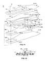
- FIG. 18is a simplified diagram showing a conventional solar cell 20 formed on a semiconductor substrate 21 .
- Semiconductor substrate 21is processed using known techniques to include an n-type doped upper region 21 A and a p-type doped lower region 21 B that collectively form a pn-junction near the center of substrate 21 .
- Formed on an upper surface 22 of semiconductor substrate 21are a series of parallel metal gridlines 25 (shown in end view) that are electrically connected to n-type region 21 A.
- a substantially solid conductive layer 26is formed on a lower surface 23 of substrate 21 , and is electrically connected to p-type region 21 B.
- An antireflection coating 27is typically formed over upper surface 22 of substrate 21 .
- Solar cell 20converts sunlight beams L 1 that pass through upper surface 22 into substrate 21 when a photon from beam L 1 hits a semiconductor material with an energy greater than the semiconductor band gap, which excites an electron (“ ⁇ ”) in the valence band to the conduction band, allowing the electron and an associated hole (“+”) to flow within substrate 21 .
- n-type region 21 A and p-type region 21 Bserves to prevent recombination of the excited electrons with the holes, thereby generating a potential difference that can be applied to a load by way of gridlines 25 and conductive layer 26 , as indicated in FIG. 18 .
- Screen printingis the predominant conventional method for producing the gridlines 25 that carry current from upper surface 22 of conventional solar cell 20 .
- Conventional screen printing techniquestypically produce gridlines having a rectangular cross-section with a width W of approximately 100 ⁇ m and a height H of approximately 15 ⁇ m, producing an aspect ratio of approximately 0.15.
- a problem associated with conventional gridlines 25 having this relatively low aspect ratiois that gridlines 25 generate an undesirably large shadowed surface area (i.e., gridlines 25 prevent sunlight from passing through a large area of upper surface 22 into substrate 21 , as depicted in FIG. 18 by light beam L 2 ), which reduces the ability of solar cell 20 to generate electricity.
- Extrusion printingis an alternative to screen printing, and involves passing an extrusion printhead over the upper surface of the solar cell substrate while extruding a metal ink.
- Extrusion printinghas an advantage over screen printing in that extrusion printing facilitates the efficient production of solar cells having high aspect ratio gridlines.
- the resulting gridline structureshave a cross-sectional shape that very closely follows the cross section of the extrusion printhead nozzle, which is typically rectangular.
- co-extrusion printinghas been introduced to solar cell production in which a metal ink is co-extruded with and encapsulated by a sacrificial ink. Co-extrusion printing can produce lines of 50 microns width and height and an aspect ratio of 1.
- the substantially flat upper surfaces of the rectangular shaped gridlinesstill reflect a significant amount of light away from the electricity generating region of the solar module.
- the use of extrusion and co-extrusion production methodshas also been found to introduce new problems.
- the high aspect ratio rectangular gridlineshave an undesirable tendency to fall on their side (i.e., tip over), which obviates the advantage of their high aspect ratio.
- the high aspect ratio extrusion processleads to stress at the silicon-silver surface that can cause delamination of the gridline.
- a micro extrusion system and associated method for forming extruded gridlines at a low costthat is acceptable to the solar cell industry and addresses the problems described above.
- a micro-extrusion system for printing high aspect ratio gridlinesthat decreases the effective shadowed surface area of the underlying substrate, helps to prevent the tipping problem of conventional rectangular extruded gridlines, and by addressing the delamination problem associated with high aspect ratio extruded gridlines.
- the present inventionis directed to a micro-extrusion system for printing high aspect ratio gridlines having a tapered (e.g., triangular or trapezoidal) cross-sectional shape that decreases the effective shadowed surface area of the underlying substrate by reflecting a higher percentage of incident light beams onto the substrate surface (i.e., instead of away from the substrate), helps to overcome the tipping problem of conventional rectangular extruded gridlines by providing a gridline structure in which the mass center is closer to the substrate surface, and helps to overcome the delamination problem by reducing the peeling moment in comparison to rectangular cross section lines.
- a taperede.g., triangular or trapezoidal
- a printhead assembly of the micro-extrusion systemincludes nozzles having a tapered (e.g., stepped, triangular or trapezoidal) cross-sectional shape such that extrusion material forced through the nozzles produces gridlines having the desired tapered cross-section.
- the nozzlesare formed by etching or otherwise forming parallel tapered grooves into a nozzle outlet structure made up of one or more plates such that each groove extends from a closed end to an open end defined in a front edge of the structure.
- a bottom plateis mounted against the nozzle outlet structure over the tapered grooves, thereby forming the desired tapered nozzles having outlet orifices formed by the open ends of the tapered grooves and the front edge of the bottom plate.
- the micro-extrusion systemalso includes a material feed system that forces material into the closed end of the tapered groove/nozzle, causing the material to fill the nozzle as it moves in a flow direction toward the outlet orifice, whereby the extruded bead is deposited on the substrate having a tapered cross-sectional shape that is essentially identical to the tapered cross-section of the extrusion nozzle.
- the nozzle outlet structureincludes one or more plates that are etched or otherwise processed to collectively form the tapered groove.
- the fluidic channels of each nozzleare fabricated by cutting or etching progressively wider channels (e.g., by laser machining, wire EDM or photochemical machining) into a series of rigid layers (e.g., stainless steel or KaptonTM layers), and then stacking the rigid layers to form a layered nozzle structure.
- a single layeris processed (e.g., using laser etching, micro EDM, anisotropically etching Si, electroforming, or injection molding) to define a groove having a triangular or trapezoidal cross-section.
- the associated micro-extrusion systemincludes a co-extrusion printhead assembly that is constructed to co-extrude two different materials in order to form closely spaced high-aspect ratio gridline structures on a substrate surface or narrow printed lines of dopant bearing paste.
- the co-extrusion printhead assemblyincludes upper an lower plate structures that serve to guide the two extrusion materials via separate conduits from corresponding inlet ports to a layered nozzle structure, and a layered nozzle structure that extrudes a bead including a sacrificial material and a gridline (functional) material arranged such that the gridline material forms a high-aspect ratio gridline structure that is supported between two sacrificial material portions (the sacrificial portions are subsequently removed).
- each three-part nozzle channelcomprise troughs defined (e.g., etched into but not through) the plate material forming the nozzle outlet plate, and a tapered groove is formed only in the central channel of the three-part nozzle channel (i.e., the channel through which the gridline material is extruded).
- each nozzleis defined only by the plate material of the nozzle outlet plate and surface portion of a bottom nozzle plate that is disposed over the open surface of each three-part nozzle channel.
- the tapered grooveextends along at least a portion of the central channel, and is formed such that a width of the upper edge of each extruded gridline bead is substantially narrower (i.e., less than one-half the width) the width of the lower end.
- the nozzle outlet orificeincludes a converging/diverging structure in which a relatively narrow section is located between the merge point and a relatively wide outlet orifice in order to lower the pressure drop in a printhead.
- FIG. 1is a simplified partial perspective view showing a portion of a micro-extrusion system including a micro-extrusion printhead assembly formed in accordance with an embodiment of the present invention
- FIG. 2is a side view showing a portion of a micro-extrusion system including a micro-extrusion printhead assembly formed in accordance with another embodiment of the present invention
- FIG. 3is a side view showing the micro-extrusion system of FIG. 2 in additional detail
- FIG. 4is an exploded cross-sectional side view showing generalized micro-extrusion printhead assembly utilized in the system of FIG. 2 ;
- FIG. 5is a partial exploded perspective view showing a three-part nozzle structure of the micro-extrusion printhead assembly of FIG. 4 ;
- FIG. 6is a partial perspective view showing the three-part nozzle structure of FIG. 5 in an assembled state
- FIG. 7is a cross-sectional side view showing a portion of the micro-extrusion printhead assembly of FIG. 4 during operation;
- FIG. 8is a front view showing a micro-extrusion system including a generalized co-extrusion printhead assembly according to another embodiment of the present invention.
- FIG. 9is an exploded perspective view showing the co-extrusion printhead assembly of FIG. 8 in additional detail
- FIG. 10is an exploded partial perspective view showing a portion of the printhead assembly of FIG. 9 in additional detail;
- FIG. 11is a simplified exploded partial perspective view showing a portion of a generalized layered nozzle structure utilized in the co-extrusion printhead assembly of FIG. 8 ;
- FIG. 12is a cross-sectional side view showing an exemplary co-extruded gridline structure generated on a substrate surface by the co-extrusion printhead assembly of FIG. 8 ;
- FIG. 13is a perspective view showing the nozzle outlet plate utilized in the co-extrusion printhead assembly of FIG. 8 in additional detail;
- FIG. 14is an enlarged perspective view showing a three-part nozzle channel formed in the nozzle outlet plate of FIG. 13 ;
- FIG. 15is a top view the three-part nozzle channel of FIG. 14 ;
- FIG. 16is a cross-sectional end view taken along section line 16 - 16 of FIG. 15 ;
- FIG. 17is a photograph showing a gridline formed by a printhead produced in accordance with the present invention.
- FIG. 18is a cross-sectional side view showing a simplified conventional solar cell.
- the present inventionrelates to an improvement in micro-extrusion systems.
- the following descriptionis presented to enable one of ordinary skill in the art to make and use the invention as provided in the context of a particular application and its requirements.
- directional termssuch as “upper”, “top”, “lower”, “bottom”, “front”, “rear”, and “lateral” are intended to provide relative positions for purposes of description, and are not intended to designate an absolute frame of reference.
- integralally moldedis used herein to describe the connective relationship between two portions of a single molded or machined structure, and are distinguished from the terms “connected” or “coupled” (without the modifier “integrally”), which indicates two separate structures that are joined by way of, for example, adhesive, fastener, clip, or movable joint.
- FIG. 1is a simplified partial perspective view showing a portion of a micro-extrusion system 50 including a micro-extrusion printhead assembly 100 for extruding a bead (gridline) 55 on an upper surface 52 of a target substrate 51 .
- the present inventionis particularly directed to printing gridlines 55 such that they have a high aspect ratio, and having a tapered (e.g., triangular or trapezoidal) cross-sectional shape. For example, as shown in FIG.
- gridline 55has a base 55 - 1 , slanted side walls 55 - 21 and 55 - 22 , and an upper ridge 55 - 3 , where an average maximum width W 2 of base 55 - 1 to average maximum height H 1 at upper ridge 55 - 3 is approximately 1 or higher.
- providing gridline with such a tapered cross-sectional shapehelps to overcome the leaning problem of conventional rectangular extruded gridlines by providing gridline 55 with a mass center M that is closer to substrate surface 52 (i.e., the height H 1 of mass center M above surface 52 is 1 ⁇ 3 or lower that of average maximum height H 1 .
- printhead assembly 100is produced such that it includes a nozzle outlet structure 160 having a front edge 168 and defining an elongated groove 162 extending from a closed end 165 to an opening that is defined through front edge 168 .
- downward-facing elongated groove 162includes a relatively wide open edge 162 - 1 having a first width w 1 , a relatively narrow closed edge 162 - 2 having a second width W 2 , which is substantially smaller width W 1 , and tapered side walls arranged to form a triangular cross-section.
- a bottom plate 156 Ais mounted on a lower surface 167 of nozzle outlet structure 160 such that an upper surface 157 A of bottom plate 156 A covers open edge 162 - 1 of groove 162 , thereby forming an extrusion nozzle 163 having a tapered (e.g., triangular) cross-section that is defined by elongated groove 162 , and extends between a closed end 165 and an outlet orifice 169 defined by the opening through front edge 168 .
- a taperede.g., triangular
- Micro-extrusion system 50also includes a material feed system 60 that forces gridline material into closed end 165 of groove 162 , causing the material to fill nozzle 163 as it moves in a flow direction F 1 toward outlet orifice 169 , whereby the extruded bead 55 is deposited on the substrate 51 to form a gridline having a tapered cross-sectional shape that is essentially identical to the tapered cross-section of extrusion nozzle 163 .
- FIG. 2is a partial side view showing a portion of a micro-extrusion system 50 A for forming parallel extruded material lines 55 A on upper surface 52 of a substrate 51 according to a second embodiment of the present invention.
- Micro-extrusion system 50 Aincludes an extrusion printhead assembly 100 A that is operably coupled to a material feed system 60 A by way of at least one feedpipe 68 and an associated fastener 69 .
- the materialsare applied through pushing and/or drawing techniques (e.g., hot and cold) in which the materials are pushed (e.g., squeezed, etc.) and/or drawn (e.g., via a vacuum, etc.) through extrusion printhead assembly 100 A, and out one or more outlet orifices (exit ports) 169 A that are respectively defined in a lower portion of printhead assembly 100 A.
- pushing and/or drawing techniquese.g., hot and cold
- extrusion printhead assembly 100 Ae.g., via a vacuum, etc.
- Micro-extrusion system 50 Aalso includes a X-Y-Z-axis positioning mechanism 70 including a mounting plate 76 for rigidly supporting and positioning printhead assembly 100 A relative to substrate 51 , and a base 80 including a platform 82 for supporting substrate 51 in a stationary position as printhead assembly 100 A is moved in a predetermined (e.g., Y-axis) direction over substrate 51 .
- a predetermined (e.g., Y-axis) direction over substrate 51e.g., Y-axis) direction over substrate 51 .
- printhead assembly 100 Ais stationary and base 80 includes an X-Y axis positioning mechanism for moving substrate 51 under printhead assembly 100 A.
- FIG. 3shows material feed system 60 A, X-Y-Z-axis positioning mechanism 70 and base 80 of micro-extrusion system 50 A in additional detail.
- the assembly shown in FIG. 3represents an experimental arrangement utilized to produce solar cells on a small scale, and those skilled in the art will recognize that other arrangements would typically be used to produce solar cells on a larger scale.
- material feed system 60 Aincludes a housing 62 that supports a pneumatic cylinder 64 , which is operably coupled to a cartridge 66 such that material is forced from cartridge 66 through feedpipe 68 into printhead assembly 100 A.
- a pneumatic cylinder 64which is operably coupled to a cartridge 66 such that material is forced from cartridge 66 through feedpipe 68 into printhead assembly 100 A.
- X-Y-Z-axis positioning mechanism 70includes a Z-axis stage 72 that is movable in the Z-axis (vertical) direction relative to target substrate 51 by way of a housing/actuator 74 using known techniques.
- Mounting plate 76is rigidly connected to a lower end of Z-axis stage 72 and supports printhead assembly 100 A, and a mounting frame 78 is rigidly connected to and extends upward from Z-axis stage 72 and supports pneumatic cylinder 64 and cartridge 66 . Referring to the lower portion of FIG.
- base 80includes supporting platform 82 , which supports target substrate 51 as an X-Y mechanism moves printhead assembly 100 A in the X-axis and Y-axis directions (as well as a couple of rotational axes) over the upper surface of substrate 51 utilizing known techniques.
- layered micro-extrusion printhead assembly 100 Aincludes a first (back) plate structure 110 , a second (front) plate structure 130 , and a layered nozzle structure 150 A connected therebetween.
- Back plate structure 110 and front plate structure 130serve to guide the extrusion material from an inlet port 116 to layered nozzle structure 150 A, and to rigidly support layered nozzle structure 150 A such that extrusion nozzle sections 163 - 1 to 163 - 3 , which are shown in FIG. 4 and collectively form nozzle 163 A in FIG. 2 , are pointed toward substrate 51 at a predetermined tilted angle ⁇ 1 (e.g., 45°; see FIG.
- extruded material traveling down extrusion nozzle sections 163 - 1 to 163 - 3 toward its corresponding nozzle orifice portions 169 - 1 to 169 - 3is directed toward target substrate 51 .
- nozzle orifice portions 169 - 1 to 169 - 3collectively form nozzle orifice 169 A in FIG. 2 .
- each of back plate structure 110 and front plate structure 130includes one or more integrally molded or machined metal parts.
- back plate structure 110includes an angled back plate 111 and a back plenum 120
- front plate structure 130includes a single-piece metal plate.
- Angled back plate 111includes a front surface 112 , a side surface 113 , and a back surface 114 , with front surface 112 and back surface 114 forming a predetermined angle ⁇ 2 (e.g., 45°; shown in FIG. 2 ).
- Angled back plate 111also defines a bore 115 that extends from a threaded countersunk bore inlet 116 defined in side wall 113 to a bore outlet 117 defined in back surface 114 .
- Back plenum 120includes parallel front surface 122 and back surface 124 , and defines a conduit 125 having an inlet 126 defined through front surface 122 , and an outlet 127 defined in back surface 124 .
- bore 115 and plenum 125cooperate to feed extrusion material to layered nozzle structure 150 .
- Front plate structure 130includes a front surface 132 and a beveled lower surface 134 that form predetermined angle ⁇ 2 (shown in FIG. 2 ).
- Layered nozzle structure 150 Aincludes two or more stacked plates (e.g., a metal such as aluminum, steel, KaptonTM or plastic) that combine to form one or more extrusion nozzles 163 A.
- layered nozzle structure 150 Aincludes a top nozzle plate 153 A, a bottom nozzle plate 156 A, and a nozzle outlet structure (plate assembly) 160 A sandwiched between top nozzle plate 153 A and bottom nozzle plate 156 A.
- Top nozzle plate 153 Adefines an inlet port (through hole) 155 A, and has a (first) front edge 158 - 1 .
- Bottom nozzle plate 156 Ais a substantially solid (i.e., continuous) plate having a (third) front edge 158 - 2 .
- Nozzle outlet structure 160 Aincludes three separate nozzle plates 160 - 1 , 160 - 2 and 160 - 3 disposed in a stacked arrangement that are described in additional detail below, and nozzle sections 163 - 1 to 163 - 3 and nozzle orifice portions 169 - 1 to 169 - 3 of nozzle plates 160 - 1 , 160 - 2 and 160 - 3 collectively form nozzle 163 A in FIG. 2 .
- nozzle outlet structure 160 Ais sandwiched between top nozzle plate 153 A and bottom nozzle plate 156 A such that nozzle sections 163 - 1 , 163 - 2 and 163 - 3 , a front portion 154 A of top nozzle plate 153 A, and a front portion 157 A of bottom nozzle plate 156 A combine to define elongated extrusion nozzle 163 A that extends from closed end 165 A to nozzle orifice 169 A.
- top nozzle plate 153 Ais mounted on nozzle outlet structure 160 A such that inlet port 155 A is aligned with closed end 165 A of nozzle assembly 163 A, whereby extrusion material forced through inlet port 155 A flows in direction F 1 along extrusion nozzle 163 A, and exits from layered nozzle structure 150 A by way of nozzle orifice 169 A to form bead 55 A on substrate 51 .
- angled back plate 111 of printhead assembly 100 Ais rigidly connected to mounting plate 76 by way of one or more fasteners (e.g., machine screws) 142 such that beveled surface 134 of front plate structure 130 is positioned close to parallel to upper surface 52 of target substrate 51 .
- fastenerse.g., machine screws
- One or more second fasteners 144are utilized to connect front plate structure 130 to back plate structure 110 with layered nozzle structure 150 A pressed between the back surface of front plate structure 130 and the back surface of back plenum 120 .
- material feed system 60 Ais operably coupled to bore 115 by way of feedpipe 68 and fastener 69 using known techniques, and extrusion material forced into bore 115 is channeled to layered nozzle structure 150 A by way of conduit 125 .
- the extrusion material exiting conduit 125enters the closed end of nozzle 163 A by way of inlet 155 A and closed end 165 A (both shown in FIG. 4 ), and flows in direction F 1 down nozzle 163 A toward outlet 169 A.
- layered micro-extrusion printhead 100 Areliably directs the extruded material toward substrate 51 in a manner that facilitates high volume solar cell production.
- FIGS. 5 and 6are simplified partial perspective views showing a portion of layered nozzle structure 150 A in additional detail.
- FIG. 5shows layers (e.g., metal or Kapton plates) 160 - 1 , 160 - 2 and 160 - 3 that are stacked as indicated in FIG. 6 to form nozzle outlet structure 160 A.
- each layer 160 - 1 , 160 - 2 and 160 - 3defines an etched groove (i.e., grooves 162 - 1 , 162 - 2 and 162 - 3 , respectively) having an associated unique width (i.e., groove 162 - 1 is narrower than groove 160 - 2 , and groove 160 - 2 is narrower than groove 160 - 3 ).
- a hardenable materialis injected into bore 115 and conduit 125 of printhead assembly 100 A in the manner described in co-owned and co-pending U.S. patent application Ser. No. 12/267,147 entitled “DEAD VOLUME REMOVAL FROM AN EXTRUSION PRINTHEAD”, which is incorporated herein by reference in its entirety.
- This hardenable materialforms portions 170 that fill any dead zones of conduit 125 that could otherwise trap the extrusion material and lead to clogs.
- At least one of the nozzle structure materials, the output geometry, and the internal conduit geometry of printhead assembly 100are modified to cause the extrusion material (bead) traveling through extrusion nozzle 163 A (i.e., in or parallel to the lateral extrusion plane E) to be reliably directed (angled) toward the target substrate as it leaves the printhead nozzle orifice.
- at least one of top nozzle plate 153 A, bottom nozzle plate 156 A, and nozzle outlet plate 160 of the layered nozzle structureis modified such that the extrusion material is directed toward substrate 51 as it exits the extrusion nozzle (i.e., the bead is directed in or downward from lateral extrusion plane E).
- the modification to printhead assembly 100takes several forms that are described in additional detail in co-owned and co-pending U.S. patent application Ser. No. 12/267,069, entitled “DIRECTIONAL EXTRUDED BEAD CONTROL”, which is incorporated by reference in its entirety.
- the extrusion beadis pressed toward the substrate in the manner described in co-owned and co-pending U.S. patent application Ser. No. 12/267,223, entitled “MICRO-EXTRUSION SYSTEM WITH AIRJET ASSISTED BEAD DEFLECTION”, which is incorporated by reference in its entirety.
- FIG. 7is a simplified cross-sectional side view showing a portion of a printhead assembly 100 A during operation.
- back plenum 120 Adefines conduit 125 that communicates with a closed end 165 A of a nozzle 163 A by way of an inlet port 155 A defined through top nozzle plate 153 A.
- portion 154 A of top nozzle plate 153 A and portion 157 A of bottom nozzle plate 156 Aform the upper and lower walls, respectively, of nozzle 163 A, whereby extrusion material entering nozzle 163 A from conduit 125 generally flows along the dashed line F 1 to outlet orifice 169 A.
- front edge of nozzle outlet structure 160 A, front edge 158 - 1 A of top nozzle plate 153 A, and front edge 158 - 2 A of bottom nozzle plate 156 Aare coplanar with front edge 128 of back plenum 120 A, forming a front edge 101 A of printhead assembly 100 A.
- FIGS. 8-12illustrate a co-extrusion system 50 E according to another embodiment of the present invention.
- Co-extrusion system 50 Eincludes a Z-axis positioning mechanism and X-Y axis positioning mechanism that are constructed and function in a manner similar to that described above with reference to FIGS. 2 and 3 .
- co-extrusion system 50 Ediffers from the above-described embodiments in that it includes material feed system 60 E having means for supplying two extrusion materials to a printhead assembly 100 E, and printhead assembly 100 E includes means for co-extruding the two extrusion materials in a manner that generates parallel high-aspect ratio gridline structures (described below with reference to FIG. 12 ).
- material feed system 60 Erepresents exemplary experimental arrangement utilized to produce solar cells on a small scale, and those skilled in the art will recognize that other arrangements would typically be used to produce solar cells on a larger scale.
- material feed system 60 Eincludes a pair of housings 62 - 1 and 62 - 2 that respectively support pneumatic cylinders 64 - 1 and 64 - 2 , which is operably coupled to cartridges 66 - 1 and 66 - 2 such that material forced from these cartridges respectively passes through feedpipes 68 - 1 and 68 - 2 into printhead assembly 100 E. As indicated in the lower portion of FIG.
- the Z-axis positioning mechanism(partially shown) includes a Z-axis stage 72 E that is movable in the Z-axis (vertical) direction by way of a housing/actuator 74 E (partially shown) using known techniques.
- Mounting plate 76 Eis rigidly connected to a lower end of Z-axis stage 72 E and supports printhead assembly 100 E, and a mounting frame (not shown) is rigidly connected to and extends upward from Z-axis stage 72 E and supports pneumatic cylinders 64 - 1 and 64 - 2 and cartridges 66 - 1 and 66 - 2 .
- FIG. 9is an exploded perspective view showing micro-extrusion printhead 100 E in additional detail.
- Micro-extrusion printhead 100 Eincludes a first (back) plate structure 110 E, a second (front) plate structure 130 E, and a layered nozzle structure 150 E connected therebetween.
- Back plate structure 110 E and front plate structure 130 Eserve to guide the extrusion material from corresponding inlet ports 116 - 1 and 116 - 2 to layered nozzle structure 150 E, and to rigidly support layered nozzle structure 150 E such that extrusion nozzles 162 E defined in layered nozzle structure 150 E are pointed toward substrate 51 at a predetermined tilted angle (e.g., 45°), whereby extruded material traveling down each extrusion nozzle 162 E toward its corresponding nozzle orifice 169 E is directed toward target substrate 51 .
- a predetermined tilted anglee.g. 45°
- back plate structure 110 Eincludes a molded or machined metal (e.g., aluminum) angled back plate 111 E, a back plenum 120 E, and a back gasket 121 disposed therebetween.
- Angled back plate 111 Eincludes a front surface 112 E, a side surface 113 E, and a back surface 114 E, with front surface 112 E and back surface 114 E forming predetermined angle ⁇ 2 (e.g., 45°).
- Angled back plate 111 Ealso defines a pair of bores (not shown) that respectively extend from threaded countersunk bore inlets 116 - 1 and 116 - 2 defined in side wall 113 E to corresponding bore outlets defined in back surface 114 E.
- Back plenum 120 Eincludes parallel front surface 122 E and back surface 124 E, and defines a pair of conduits (not shown) extending from corresponding inlets 126 - 1 and 126 - 2 defined through front surface 122 to corresponding outlets (not shown) defined in back surface 124 E. Similar to the description provided above, the bores/conduits defined through back plate structure 110 E feed extrusion material to layered nozzle structure 150 E.
- front plate structure 130 Eincludes a molded or machined metal (e.g., aluminum) front plate 131 E, a front plenum 140 E, and a front gasket 141 disposed therebetween.
- Front plate 131 Eincludes a front surface 132 E, a side surface 133 E, and a beveled back surface 134 E, with front surface 132 E and back surface 134 E forming the predetermined angle described above.
- Front plate 131 Edefines several holes for attaching to other sections of printhead assembly 100 E, but does not channel extrusion material.
- Front plenum 140 Eincludes parallel front surface 142 E and back surface 144 E, and defines a conduit (not shown) extending from corresponding inlet 148 to a corresponding outlet 149 , both being defined through front surface 142 E.
- the conduit defined in front plenum 140 Eserves to feed one of the extrusion materials to layered nozzle structure 150 E.
- layered nozzle structure 150 Eincludes a top nozzle plate 153 E, a bottom nozzle plate 156 E, and a nozzle outlet plate (structure) 160 E sandwiched between top nozzle plate 153 E and bottom nozzle plate 156 E.
- top nozzle plate 153 Edefines a row of substantially circular inlet ports (through holes) 155 - 1 E and a corresponding series of elongated inlet ports 155 - 2 E that are aligned adjacent to a front edge 158 - 1 E.
- Bottom nozzle plate 156 Eis a substantially solid (i.e., continuous) plate having a front edge 158 - 2 E, and defines several through holes 159 - 6 E, whose purpose is described below.
- Nozzle outlet plate 160 Eincludes a front edge 168 E, and defines a row of three-part nozzles 162 E that are described in additional detail below, and several through holes 159 - 7 E that are aligned with through holes 159 - 6 E.
- nozzle outlet plate 160 EWhen operably assembled, nozzle outlet plate 160 E is sandwiched between top nozzle plate 153 E and bottom nozzle plate 156 E to form a series of nozzles in which each three-part nozzle channel 162 E is enclosed by corresponding portions of top nozzle plate 153 E and bottom nozzle plate 156 E in the manner described above, with each part of three-part nozzle channel 162 E aligned to receive material from two inlet ports 155 - 1 E and one elongated inlet port 155 - 2 E.
- this arrangementproduces parallel high-aspect ratio gridline structures (beads) in which a gridline material is pressed between two sacrificial material sections.
- layered nozzle structure 150 Ealso includes a first feed layer plate 151 and a second feed layer plate 152 that are stacked over top nozzle plate 153 E and served to facilitate the transfer of the two extrusion materials to nozzle outlet plate 160 E in the desired manner described below.
- First feed layer plate 151is a substantially solid (i.e., continuous) plate having a (fourth) front edge 158 - 4 E, and defines several Y-shaped through holes 155 - 3 E located adjacent to front edge 158 - 4 E, and several feed holes 159 - 1 E whose purposes are described below.
- Second feed layer plate 152is disposed immediately below first feel layer plate 151 , includes a (fifth) front edge 158 - 5 E, and defines several substantially circular through holes 155 - 4 E located adjacent to front edge 158 - 5 E, and several feed holes 159 - 2 E whose purposes are described below.
- two extrusion materialsare fed by way of two separate paths in a substantially Z-axis direction through the various layers of layered nozzle structure 150 E to nozzle outlet plate 160 E.
- the two flow pathsare described in detail in the following paragraphs.
- gridline material 56 injected through inlet port 116 - 1is fed downward through opening 121 - 1 in back gasket 121 and into opening 126 - 1 defined in back plenum 120 E.
- the gridline materialthen exits back plenum 120 E and passes through aligned openings 159 - 1 E to 159 - 5 E respectively formed in first feed layer plate 151 , second feed layer plate 152 , top nozzle plate 153 E, nozzle outlet plate 160 E, and bottom nozzle plate 156 E before entering opening 149 - 1 of front plenum 140 E.
- the gridline materialis then redirected by front plenum 140 E and moves upward from opening 149 - 2 through opening 159 - 6 E formed in bottom nozzle plate 156 E and opening 159 - 7 E formed in nozzle outlet plate 160 E.
- the gridline materialthen enters the rearward end of elongated openings 159 - 7 E, and is redirected in a substantially horizontal direction along arrow F 1 A to the front end of elongated opening 159 - 7 E.
- the gridline materialis then forced downward into a central channel 167 of three-part nozzle channel 162 E.
- the gridline materialthen flows along central channel 167 E in the direction of arrow F 1 , and is compressed between corresponding sacrificial material portions before exiting from orifice 169 E.
- sacrificial material 57 injected through inlet port 116 - 2is fed downward through opening 121 - 2 in back gasket 121 and into opening 126 - 2 defined in back plenum 120 E.
- the sacrificial materialis dispersed by plenum 120 E and is passed into the rearward end of Y-shaped elongated channels 155 - 3 E, which are formed in first feed layer plate 151 .
- the sacrificial materialflows along each Y-shaped elongated channel 155 - 3 E to a split front end region, where the sacrificial material is distributed through corresponding openings 155 - 4 E disposed in second feed layer plate 152 and openings 155 - 1 E disposed in top nozzle plate 153 E, and then into opposing side channel 165 E of three-part nozzle channel 162 E. As described in additional detail below, the sacrificial material then flows along side channels 165 E, and presses against the corresponding gridline material before exiting from orifice 169 E.
- nozzle output plate 160 Eincludes a plate that is micro-machined (e.g., using deep reactive ion etching) to include arrowhead-shaped three-part nozzle channel 162 E including a central channel 167 E and opposing (first and second) side channels 165 E.
- Central channel 167 Eis separated from each side channel 165 E by an associated tapered finger of plate material.
- Central channel 167 Ehas a closed end that is aligned to receive gridline material from the front end of elongated opening 159 - 7 E of top nozzle plate 153 E, and an open end that communicates with a merge point 166 E.
- side channels 165 Ehave associated closed ends that are aligned to receive sacrificial material from corresponding openings 155 - 1 E of top nozzle plate 153 E, and open ends that communicate with a merge point 166 E.
- Side channels 165 Eare angled toward central channel 167 E such that sacrificial material is fed against opposing sides of the gridline material flowing in central channel 167 E.
- the gridline material and sacrificial material co-extruded through each nozzle outlet orifice 169 E (see FIG. 11 ) of co-extrusion printhead assembly 100 E during the extrusion processforms an elongated extruded structure 55 E on surface 52 of substrate 51 such that the gridline material of each structure 55 E forms a high-aspect ratio gridline structure 56 , and such that the sacrificial material of each structure 55 E forms associated first and second sacrificial material portions 57 - 1 and 57 - 2 respectively disposed on opposing sides of the associated high-aspect ratio gridline 56 .
- extruded structures 55 Ei.e., the aspect ratio of gridline material 56 and the shape of sacrificial portions 57 - 1 and 57 - 2
- shape of extruded structures 55 Eare controllable through at least one of the shapes of the one or more outlet orifices and internal geometry of printhead assembly 100 E, characteristics of the materials (e.g., viscosity, etc.), and the extrusion technique (e.g., flow rate, pressure, temperature, etc.).
- the shape of bead 55 Eis made to conform to the goals set forth above (i.e., such that a base of each bead 55 E has a substantially wider width W 2 than the width W 2 of the upper bead edge).
- Suitable gridline materials 56include, but are not limited to, silver, copper, nickel, tin, aluminum, steel, alumina, silicates, glasses, carbon black, polymers and waxes, and suitable sacrificial materials 112 include plastic, ceramic, oil, cellulose, latex, polymethylmethacrylate etc., combinations thereof, and/or variations thereof, including combining the above with other substances to obtain a desired density, viscosity, texture, color, etc.
- extruded beads leaving co-extrusion printhead 100 Ecan be quenched on substrate 51 by cooling the substrate using known techniques.
- the gridline (ink) material usedmay be a hot-melt material, which solidifies at ambient temperatures, in which case co-extrusion printhead 100 E is heated, leaving the extruded structures to solidify once they are dispensed onto substrate 51 .
- the materialscan be cured by thermal, optical and/or other means upon exit from co-extrusion printhead 100 E.
- a curing componentcan be provided to thermally and/or optically cure the materials. If one or both materials include an ultraviolet curing agent, the material can be bound up into solid form in order to enable further processing without mixing.
- FIGS. 13-16illustrate nozzle outlet plate 160 E in additional detail.
- FIG. 13is a perspective bottom view showing nozzle outlet plate 160 E
- FIGS. 14 , 15 and 16are enlarged bottom perspective, bottom plan and cross-sectional elevation views showing a portion of nozzle outlet plate 160 E including an exemplary three-part nozzle channel 162 E of nozzle outlet plate 160 E in additional detail.
- three-part nozzle channel 162 Eincludes two trough-like side channels 165 E and a trough-like central channel 167 E that converge at a merge point 166 E in the manner described above, and an outlet orifice 169 E defined in a front edge 168 E of the plate material forming nozzle outlet plate 160 E.
- each channel of three-part nozzle channel 162 Ecomprises a trough-like cavity having a bottom surface formed by the plate material used to fabricate nozzle outlet plate 160 E.
- Such trough-like cavitiesare formed, for example, by photochemical machining, electro-discharge machining or by laser ablating metal sheet stock, or by using deep reactive ion etching on a variety of materials, all by known techniques.
- each nozzle 163 Eis defined only by the plate material of nozzle outlet plate 160 F that forms each trough, and bottom nozzle plate 156 E (not shown in FIG. 14 ) that is disposed over the open (bottom) surface of each three-part nozzle channel 162 F.
- openings 161 - 1 to 161 - 3are etched through the plate material of nozzle outlet plate 160 E in order to facilitate the flow of gridline and sacrificial material into side channels 165 E and central channel 167 E from corresponding openings formed in an associated top nozzle plate (not shown).
- a tapered elongated groove 162 E- 1similar to tapered groove 162 A described above, is defined only in the central portion of central channel 167 E.
- elongated groove 162 E- 1has a trapezoid-shaped cross-section adjacent to opening 161 E (i.e., adjacent to the closed end of central channel 167 E), and tapers to a substantially triangular cross-section adjacent to outlet orifice 169 E.
- the upper portion of the functional materialis squeezed together to form beads (e.g., bead 55 E; see FIG. 12 ) having the desired tapered cross-section.
- nozzle outlet plate 160 Ehas a converging/diverging orifice structure in which a relatively narrow section 169 - 1 having a width W 1 is located between the relatively wide merge point 166 E (i.e., having a width W 2 ) and a relatively wide open end 169 E- 2 of outlet orifice 169 e , which has a width W 3 .
- This converging/diverging arrangementlowers the pressure drop in a printhead incorporating nozzle outlet plate 160 E, thereby enabling one or more of higher speed printing and lower pressure operation.
- Increased print speedis beneficial for the printer productivity, lowered operating pressure is beneficial for increasing printhead reliability and lowering printhead weight and cost.
- the extrusion printheads of the present inventioncan be manufactured by electroplating metal up through features in a patterned resist structure, by brazing together layers of etched plate metal, by generating structures out of photo-definable polymer such as SU8, or by machining or molding.
- FIG. 17is an SEM generated cross-sectional image of an extruded line (bead) 55 E formed on a substrate 51 E, wherein line 55 E was printed using a coextrusion nozzle with a stepwise triangular metal inlet feed similar to that described above with reference to FIG. 6 .
- bead 55 Ehas sloped sidewalls, and a narrowed flat section at the top. This structure is desired for shadowing reasons as detailed above.
Landscapes
- Engineering & Computer Science (AREA)
- Mechanical Engineering (AREA)
- Manufacturing & Machinery (AREA)
- Microelectronics & Electronic Packaging (AREA)
- Coating Apparatus (AREA)
Abstract
Description
Claims (7)
Priority Applications (1)
| Application Number | Priority Date | Filing Date | Title |
|---|---|---|---|
| US12/266,974US8226391B2 (en) | 2006-11-01 | 2008-11-07 | Micro-extrusion printhead nozzle with tapered cross-section |
Applications Claiming Priority (2)
| Application Number | Priority Date | Filing Date | Title |
|---|---|---|---|
| US11/555,496US7922471B2 (en) | 2006-11-01 | 2006-11-01 | Extruded structure with equilibrium shape |
| US12/266,974US8226391B2 (en) | 2006-11-01 | 2008-11-07 | Micro-extrusion printhead nozzle with tapered cross-section |
Related Parent Applications (1)
| Application Number | Title | Priority Date | Filing Date |
|---|---|---|---|
| US11/555,496Continuation-In-PartUS7922471B2 (en) | 2006-11-01 | 2006-11-01 | Extruded structure with equilibrium shape |
Publications (2)
| Publication Number | Publication Date |
|---|---|
| US20090057944A1 US20090057944A1 (en) | 2009-03-05 |
| US8226391B2true US8226391B2 (en) | 2012-07-24 |
Family
ID=40406184
Family Applications (1)
| Application Number | Title | Priority Date | Filing Date |
|---|---|---|---|
| US12/266,974Active2028-10-17US8226391B2 (en) | 2006-11-01 | 2008-11-07 | Micro-extrusion printhead nozzle with tapered cross-section |
Country Status (1)
| Country | Link |
|---|---|
| US (1) | US8226391B2 (en) |
Cited By (3)
| Publication number | Priority date | Publication date | Assignee | Title |
|---|---|---|---|---|
| US20170197347A1 (en)* | 2010-03-25 | 2017-07-13 | 3M Innovative Properties Company | Composite layer |
| US10526729B2 (en) | 2014-02-24 | 2020-01-07 | Nanofiber, Inc. | Melt blowing die, apparatus and method |
| US20230113429A1 (en)* | 2020-03-26 | 2023-04-13 | Nordson Corporation | Nozzle, adhesive application head, adhesive application apparatus, and method of making diaper |
Families Citing this family (7)
| Publication number | Priority date | Publication date | Assignee | Title |
|---|---|---|---|---|
| DE102009020029A1 (en)* | 2009-05-05 | 2010-11-11 | Feindrahtwerk Adolf Edelhoff Gmbh & Co. Kg | Electrical contacting element for photovoltaic cells, particularly solar cells, has cross-sectional profile of wires with continuous contour |
| JP5629767B2 (en)* | 2009-06-09 | 2014-11-26 | ヴィデオジェット テクノロジーズ インコーポレイテッド | Flow printing method |
| DE102009037217A1 (en)* | 2009-08-12 | 2011-02-17 | Solarworld Innovations Gmbh | Method for producing a semiconductor device |
| JP5267519B2 (en)* | 2009-09-04 | 2013-08-21 | カシオ計算機株式会社 | Discharge unit, coating apparatus, and coating method |
| US9643394B2 (en)* | 2011-02-01 | 2017-05-09 | Palo Alto Research Center Incorporated | Oblique angle micromachining of fluidic structures |
| WO2018191207A1 (en)* | 2017-04-10 | 2018-10-18 | Roche Diabetes Care, Inc. | Multi-reagent slot die coating process and useful devices |
| US11292016B2 (en)* | 2018-03-16 | 2022-04-05 | The Procter & Gamble Company | Nozzle assembly used to manufacture absorbent articles |
Citations (198)
| Publication number | Priority date | Publication date | Assignee | Title |
|---|---|---|---|---|
| US2031387A (en) | 1934-08-22 | 1936-02-18 | Schwarz Arthur | Nozzle |
| US2326803A (en) | 1941-03-18 | 1943-08-17 | Samiran David | Positive displacement pump for metering |
| US2761791A (en) | 1955-02-23 | 1956-09-04 | Eastman Kodak Co | Method of multiple coating |
| US2789731A (en) | 1955-06-06 | 1957-04-23 | Leonard L Marraffino | Striping dispenser |
| US3032008A (en) | 1956-05-07 | 1962-05-01 | Polaroid Corp | Apparatus for manufacturing photographic films |
| US3159313A (en) | 1961-05-16 | 1964-12-01 | Dow Chemical Co | Multi-component proportioning meter system |
| US3176345A (en)* | 1962-06-25 | 1965-04-06 | Monsanto Co | Spinnerette |
| US3204290A (en)* | 1962-12-27 | 1965-09-07 | Monsanto Co | Laminated spinneret |
| US3492692A (en)* | 1967-02-07 | 1970-02-03 | Japan Exlan Co Ltd | Apparatus for spinning composite fibers |
| US3602193A (en) | 1969-04-10 | 1971-08-31 | John R Adams | Apparatus for preparing coatings with extrusions |
| US3973994A (en) | 1974-03-11 | 1976-08-10 | Rca Corporation | Solar cell with grooved surface |
| US3988166A (en) | 1975-01-07 | 1976-10-26 | Beam Engineering, Inc. | Apparatus for enhancing the output of photovoltaic solar cells |
| US4018367A (en) | 1976-03-02 | 1977-04-19 | Fedco Inc. | Manifold dispensing apparatus having releasable subassembly |
| US4021267A (en) | 1975-09-08 | 1977-05-03 | United Technologies Corporation | High efficiency converter of solar energy to electricity |
| US4045246A (en) | 1975-08-11 | 1977-08-30 | Mobil Tyco Solar Energy Corporation | Solar cells with concentrators |
| US4053327A (en) | 1975-09-24 | 1977-10-11 | Communications Satellite Corporation | Light concentrating solar cell cover |
| US4084985A (en) | 1977-04-25 | 1978-04-18 | The United States Of America As Represented By The Administrator Of The National Aeronautics And Space Administration | Method for producing solar energy panels by automation |
| US4086485A (en) | 1976-05-26 | 1978-04-25 | Massachusetts Institute Of Technology | Solar-radiation collection apparatus with tracking circuitry |
| US4095997A (en) | 1976-10-07 | 1978-06-20 | Griffiths Kenneth F | Combined solar cell and hot air collector apparatus |
| US4119058A (en) | 1976-03-11 | 1978-10-10 | Alfred Schmermund | Glue applicators |
| US4131485A (en) | 1977-08-08 | 1978-12-26 | Motorola, Inc. | Solar energy collector and concentrator |
| US4141231A (en) | 1975-07-28 | 1979-02-27 | Maschinenfabrik Peter Zimmer Aktiengesellschaft | Machine for applying patterns to a substrate |
| US4148301A (en) | 1977-09-26 | 1979-04-10 | Cluff C Brent | Water-borne rotating solar collecting and storage systems |
| US4153476A (en) | 1978-03-29 | 1979-05-08 | Nasa | Double-sided solar cell package |
| US4177083A (en) | 1977-09-06 | 1979-12-04 | Acurex Corporation | Photovoltaic concentrator |
| US4221468A (en) | 1979-02-26 | 1980-09-09 | Macken John A | Multi-cavity laser mirror |
| US4224081A (en) | 1974-11-27 | 1980-09-23 | Sharp Kabushiki Kaisha | Solar cell sealed by glass laminations |
| US4254894A (en) | 1979-08-23 | 1981-03-10 | The Continental Group, Inc. | Apparatus for dispensing a striped product and method of producing the striped product |
| US4331703A (en) | 1979-03-28 | 1982-05-25 | Solarex Corporation | Method of forming solar cell having contacts and antireflective coating |
| US4337758A (en) | 1978-06-21 | 1982-07-06 | Meinel Aden B | Solar energy collector and converter |
| US4355196A (en) | 1981-03-11 | 1982-10-19 | The United States Of America As Represented By The Administrator Of The National Aeronautics And Space Administration | Solar cell having improved back surface reflector |
| US4420510A (en) | 1982-03-23 | 1983-12-13 | Weyerhaeuser Company | Method for applying a foamed adhesive under start-stop conditions |
| US4461403A (en) | 1980-12-17 | 1984-07-24 | Colgate-Palmolive Company | Striping dispenser |
| US4476165A (en) | 1982-06-07 | 1984-10-09 | Acumeter Laboratories, Inc. | Method of and apparatus for multi-layer viscous fluid deposition such as for the application of adhesives and the like |
| US4490418A (en) | 1982-04-16 | 1984-12-25 | Fuji Photo Film Co., Ltd. | Coating method and apparatus |
| JPS6082680A (en) | 1983-10-07 | 1985-05-10 | Fuji Photo Film Co Ltd | Surface treating device for metallic web |
| US4521457A (en) | 1982-09-21 | 1985-06-04 | Xerox Corporation | Simultaneous formation and deposition of multiple ribbon-like streams |
| US4540843A (en) | 1983-03-09 | 1985-09-10 | Licentia Patent-Verwaltungs-Gmbh | Solar cell |
| US4602120A (en) | 1983-11-25 | 1986-07-22 | Atlantic Richfield Company | Solar cell manufacture |
| US4683348A (en) | 1985-04-26 | 1987-07-28 | The Marconi Company Limited | Solar cell arrays |
| US4746370A (en) | 1987-04-29 | 1988-05-24 | Ga Technologies Inc. | Photothermophotovoltaic converter |
| US4747517A (en) | 1987-03-23 | 1988-05-31 | Minnesota Mining And Manufacturing Company | Dispenser for metering proportionate increments of polymerizable materials |
| US4792685A (en) | 1987-04-29 | 1988-12-20 | Masami Yamakawa | Photoelectric sensor |
| US4796038A (en) | 1985-07-24 | 1989-01-03 | Ateq Corporation | Laser pattern generation apparatus |
| US4826777A (en) | 1987-04-17 | 1989-05-02 | The Standard Oil Company | Making a photoresponsive array |
| US4841946A (en) | 1984-02-17 | 1989-06-27 | Marks Alvin M | Solar collector, transmitter and heater |
| US4847349A (en) | 1985-08-27 | 1989-07-11 | Mitsui Toatsu Chemicals, Inc. | Polyimide and high-temperature adhesive of polyimide from meta substituted phenoxy diamines |
| US4849028A (en) | 1986-07-03 | 1989-07-18 | Hughes Aircraft Company | Solar cell with integrated interconnect device and process for fabrication thereof |
| US4855884A (en) | 1987-12-02 | 1989-08-08 | Morpheus Lights, Inc. | Variable beamwidth stage light |
| US4938994A (en) | 1987-11-23 | 1990-07-03 | Epicor Technology, Inc. | Method and apparatus for patch coating printed circuit boards |
| US4947825A (en) | 1989-09-11 | 1990-08-14 | Rockwell International Corporation | Solar concentrator - radiator assembly |
| US4952026A (en) | 1988-10-14 | 1990-08-28 | Corning Incorporated | Integral optical element and method |
| US4985715A (en) | 1990-03-22 | 1991-01-15 | Telesis Controls Corporation | Marker assembly for spray marking dot matrix characters and method of fabrication thereof |
| US5000988A (en) | 1987-01-14 | 1991-03-19 | Matsushita Electric Industrial Co., Ltd. | Method of applying a coating of viscous materials |
| US5004319A (en) | 1988-12-29 | 1991-04-02 | The United States Of America As Represented By The Department Of Energy | Crystal diffraction lens with variable focal length |
| US5011565A (en) | 1989-12-06 | 1991-04-30 | Mobil Solar Energy Corporation | Dotted contact solar cell and method of making same |
| US5062899A (en) | 1990-03-30 | 1991-11-05 | The United States Of America As Represented By The Administrator Of The National Aeronautics And Space Administration | Wide acceptance angle, high concentration ratio, optical collector |
| US5075281A (en) | 1989-01-03 | 1991-12-24 | Testardi Louis R | Methods of making a high dielectric constant, resistive phase of YBA2 CU3 OX and methods of using the same |
| US5089055A (en) | 1989-12-12 | 1992-02-18 | Takashi Nakamura | Survivable solar power-generating systems for use with spacecraft |
| US5120484A (en) | 1991-03-05 | 1992-06-09 | The Cloeren Company | Coextrusion nozzle and process |
| US5151377A (en) | 1991-03-07 | 1992-09-29 | Mobil Solar Energy Corporation | Method for forming contacts |
| US5167724A (en) | 1991-05-16 | 1992-12-01 | The United States Of America As Represented By The United States Department Of Energy | Planar photovoltaic solar concentrator module |
| US5180441A (en) | 1991-06-14 | 1993-01-19 | General Dynamics Corporation/Space Systems Division | Solar concentrator array |
| US5188789A (en) | 1990-09-14 | 1993-02-23 | Fuji Photo Film Co., Ltd. | Producing a photographic support |
| US5213628A (en) | 1990-09-20 | 1993-05-25 | Sanyo Electric Co., Ltd. | Photovoltaic device |
| US5216543A (en) | 1987-03-04 | 1993-06-01 | Minnesota Mining And Manufacturing Company | Apparatus and method for patterning a film |
| US5254388A (en) | 1990-12-21 | 1993-10-19 | Minnesota Mining And Manufacturing Company | Light control film with reduced ghost images |
| US5344496A (en) | 1992-11-16 | 1994-09-06 | General Dynamics Corporation, Space Systems Division | Lightweight solar concentrator cell array |
| US5353813A (en) | 1992-08-19 | 1994-10-11 | Philip Morris Incorporated | Reinforced carbon heater with discrete heating zones |
| US5356488A (en) | 1991-12-27 | 1994-10-18 | Rudolf Hezel | Solar cell and method for its manufacture |
| WO1994028361A1 (en) | 1993-06-02 | 1994-12-08 | Stirbl Robert C | Method for changing solar energy distribution |
| US5389159A (en) | 1992-09-01 | 1995-02-14 | Canon Kabushiki Kaisha | Solar cell module and method for producing the same |
| US5449413A (en) | 1993-05-12 | 1995-09-12 | Optical Coating Laboratory, Inc. | UV/IR reflecting solar cell cover |
| US5501743A (en) | 1994-08-11 | 1996-03-26 | Cherney; Matthew | Fiber optic power-generating system |
| US5529054A (en) | 1994-06-20 | 1996-06-25 | Shoen; Neil C. | Solar energy concentrator and collector system and associated method |
| US5536313A (en) | 1993-09-06 | 1996-07-16 | Matsushita Electric Industrial Co., Ltd. | Intermittent coating apparatus |
| US5538563A (en) | 1995-02-03 | 1996-07-23 | Finkl; Anthony W. | Solar energy concentrator apparatus for bifacial photovoltaic cells |
| US5540216A (en) | 1994-11-21 | 1996-07-30 | Rasmusson; James K. | Apparatus and method for concentrating radiant energy emanated by a moving energy source |
| US5543333A (en) | 1993-09-30 | 1996-08-06 | Siemens Solar Gmbh | Method for manufacturing a solar cell having combined metallization |
| US5552820A (en) | 1993-05-21 | 1996-09-03 | Xerox Corporation | Fly's eye optics for a raster output scanner in an electrophotographic printer |
| US5559677A (en) | 1994-04-29 | 1996-09-24 | Motorola, Inc. | Method of forming a device by selectively thermal spraying a metallic conductive material thereon |
| US5560518A (en) | 1992-02-25 | 1996-10-01 | Cambridge Consultants Limited | Fluid delivery system |
| US5569399A (en) | 1995-01-20 | 1996-10-29 | General Electric Company | Lasing medium surface modification |
| US5590818A (en) | 1994-12-07 | 1997-01-07 | Smithkline Beecham Corporation | Mulitsegmented nozzle for dispensing viscous materials |
| US5605720A (en) | 1996-04-04 | 1997-02-25 | J & M Laboratories Inc. | Method of continuously formulating and applying a hot melt adhesive |
| US5665175A (en) | 1990-05-30 | 1997-09-09 | Safir; Yakov | Bifacial solar cell |
| US5679379A (en) | 1995-01-09 | 1997-10-21 | Fabbricante; Anthony S. | Disposable extrusion apparatus with pressure balancing modular die units for the production of nonwoven webs |
| US5700325A (en) | 1994-08-03 | 1997-12-23 | Matsushita Electric Industrial Co., Ltd. | Coating device and a method of coating |
| US5733608A (en) | 1995-02-02 | 1998-03-31 | Minnesota Mining And Manufacturing Company | Method and apparatus for applying thin fluid coating stripes |
| DE19735281A1 (en) | 1997-08-14 | 1999-02-18 | Rolf Hoericht | Energy generating arrangement using solar radiation |
| US5873495A (en) | 1996-11-21 | 1999-02-23 | Saint-Germain; Jean G. | Device for dispensing multi-components from a container |
| US5918771A (en) | 1996-01-31 | 1999-07-06 | Airspray International B.V. | Aerosol intended for dispensing a multi-component material |
| US5929530A (en) | 1995-08-18 | 1999-07-27 | Mcdonnell Douglas Corporation | Advanced solar controller |
| US5949123A (en) | 1995-11-13 | 1999-09-07 | Photowatt International S.A. | Solar cell including multi-crystalline silicon and a method of texturizing the surface of p-type multi-crystalline silicon |
| US5981902A (en) | 1994-12-15 | 1999-11-09 | Mitsubishi Chemical Corporation | Texturing apparatus for magnetic recording medium and magnetic recording medium process thereby |
| US5990413A (en) | 1996-06-19 | 1999-11-23 | Ortabasi; Ugur | Bifacial lightweight array for solar power |
| US6008449A (en) | 1997-08-19 | 1999-12-28 | Cole; Eric D. | Reflective concentrating solar cell assembly |
| US6011307A (en) | 1997-08-12 | 2000-01-04 | Micron Technology, Inc. | Anisotropic conductive interconnect material for electronic devices, method of use and resulting product |
| US6020554A (en) | 1999-03-19 | 2000-02-01 | Photovoltaics International, Llc | Tracking solar energy conversion unit adapted for field assembly |
| US6032997A (en) | 1998-04-16 | 2000-03-07 | Excimer Laser Systems | Vacuum chuck |
| US6047862A (en) | 1995-04-12 | 2000-04-11 | Smithkline Beecham P.L.C. | Dispenser for dispensing viscous fluids |
| US6091017A (en) | 1999-08-23 | 2000-07-18 | Composite Optics Incorporated | Solar concentrator array |
| WO2000049421A1 (en) | 1999-02-16 | 2000-08-24 | Alien Technology Corporation | Testing integrated circuit dice |
| WO2000049658A1 (en) | 1999-02-16 | 2000-08-24 | Alien Technology Corporation | Functionally symmetric integrated circuit die |
| US6118067A (en) | 1998-11-20 | 2000-09-12 | Swales Aerospace | Method and apparatus for improved solar concentration arrays |
| US6130465A (en) | 1997-10-29 | 2000-10-10 | Light Point Systems Inc. | Micro-solar assembly |
| US6140570A (en) | 1997-10-29 | 2000-10-31 | Canon Kabushiki Kaisha | Photovoltaic element having a back side transparent and electrically conductive layer with a light incident side surface region having a specific cross section and a module comprising said photovolatic element |
| US6164633A (en) | 1999-05-18 | 2000-12-26 | International Business Machines Corporation | Multiple size wafer vacuum chuck |
| US6203621B1 (en) | 1999-05-24 | 2001-03-20 | Trw Inc. | Vacuum chuck for holding thin sheet material |
| US6232217B1 (en) | 2000-06-05 | 2001-05-15 | Chartered Semiconductor Manufacturing Ltd. | Post treatment of via opening by N-containing plasma or H-containing plasma for elimination of fluorine species in the FSG near the surfaces of the via opening |
| US6257450B1 (en) | 1999-04-21 | 2001-07-10 | Pechiney Plastic Packaging, Inc. | Dual dispense container having cloverleaf orifice |
| US20010008230A1 (en) | 1996-07-08 | 2001-07-19 | David M. Keicher | Energy-beam-driven rapid fabrication system |
| US6274508B1 (en) | 1999-02-05 | 2001-08-14 | Alien Technology Corporation | Apparatuses and methods used in forming assemblies |
| US6278054B1 (en) | 1998-05-28 | 2001-08-21 | Tecstar Power Systems, Inc. | Solar cell having an integral monolithically grown bypass diode |
| US6293498B1 (en) | 1996-06-28 | 2001-09-25 | Honeywell International Inc. | Hybrid deicing system and method of operation |
| US6310281B1 (en) | 2000-03-16 | 2001-10-30 | Global Solar Energy, Inc. | Thin-film, flexible photovoltaic module |
| US6323415B1 (en) | 1998-09-18 | 2001-11-27 | Hitachi, Ltd. | Light concentrator photovoltaic module method of manufacturing same and light concentrator photovoltaic system |
| US20010053420A1 (en) | 1999-06-02 | 2001-12-20 | Nordson Corporation | Air assisted liquid dispensing apparatus and method for increasing contact area between the liquid and a substrate |
| USRE37512E1 (en) | 1995-02-21 | 2002-01-15 | Interuniversitair Microelektronica Centrum (Imec) Vzw | Method of preparing solar cell front contacts |
| US6351098B1 (en) | 1999-10-05 | 2002-02-26 | Kabushiki Kaisha Toyoda Jidoshokki Seisakusho | Charging receptacle |
| US6354791B1 (en) | 1997-04-11 | 2002-03-12 | Applied Materials, Inc. | Water lift mechanism with electrostatic pickup and method for transferring a workpiece |
| JP2002111035A (en) | 2000-09-27 | 2002-04-12 | Sanyo Electric Co Ltd | Double-sided solar cell module |
| US6375311B1 (en) | 1997-11-07 | 2002-04-23 | Fuji Xerox Co., Ltd. | Image forming apparatus and image forming method using an extrusion opening and shutter for releasing recording solution |
| US6379521B1 (en) | 1998-01-06 | 2002-04-30 | Canon Kabushiki Kaisha | Method of producing zinc oxide film, method of producing photovoltaic element, and method of producing semiconductor element substrate |
| US20020056473A1 (en) | 2000-11-16 | 2002-05-16 | Mohan Chandra | Making and connecting bus bars on solar cells |
| US20020060208A1 (en) | 1999-12-23 | 2002-05-23 | Xinbing Liu | Apparatus for drilling holes with sub-wavelength pitch with laser |
| US6398370B1 (en) | 2000-11-15 | 2002-06-04 | 3M Innovative Properties Company | Light control device |
| US6407329B1 (en) | 1999-04-07 | 2002-06-18 | Bridgestone Corporation | Backside covering member for solar battery, sealing film and solar battery |
| US6410843B1 (en) | 1999-11-22 | 2002-06-25 | Sanyo Electric Co., Ltd. | Solar cell module |
| US20020083895A1 (en) | 2000-03-14 | 2002-07-04 | Nordson Corporation | Device and method for applying adhesive filaments to materials such as strands or flat substrates |
| US6418986B1 (en) | 1997-07-01 | 2002-07-16 | Smithkline Beecham Corporation | Nozzle apparatus, a device for inserting materials into a container using such nozzle apparatus, and a container containing materials inserted therein with the use of such device |
| US6420266B1 (en) | 1999-11-02 | 2002-07-16 | Alien Technology Corporation | Methods for creating elements of predetermined shape and apparatuses using these elements |
| US6423140B1 (en) | 2000-06-08 | 2002-07-23 | Formosa Advanced Coating Technologies, Inc. | Die set for preparing ABCABC multiple-stripe coating |
| US6429037B1 (en) | 1998-06-29 | 2002-08-06 | Unisearch Limited | Self aligning method for forming a selective emitter and metallization in a solar cell |
| US20020148497A1 (en) | 2001-03-23 | 2002-10-17 | Makoto Sasaoka | Concentrating photovoltaic module and concentrating photovoltaic power generating system |
| US20020149107A1 (en) | 2001-02-02 | 2002-10-17 | Avery Dennison Corporation | Method of making a flexible substrate containing self-assembling microstructures |
| US20020154396A1 (en) | 1998-03-20 | 2002-10-24 | Overbeck James W. | Wide field of view and high speed scanning microscopy |
| US6479395B1 (en) | 1999-11-02 | 2002-11-12 | Alien Technology Corporation | Methods for forming openings in a substrate and apparatuses with these openings and methods for creating assemblies with openings |
| WO2002097724A1 (en) | 2001-05-31 | 2002-12-05 | Alien Technology Corporation | Multi-feature-size electronic structures |
| US20030015820A1 (en) | 2001-06-15 | 2003-01-23 | Hidekazu Yamazaki | Method of producing of cellulose ester film |
| US6527964B1 (en) | 1999-11-02 | 2003-03-04 | Alien Technology Corporation | Methods and apparatuses for improved flow in performing fluidic self assembly |
| US6529220B1 (en) | 1999-09-06 | 2003-03-04 | Fuji Photo Film Co., Ltd. | Method and apparatus for forming image with image recording liquid and dummy liquid |
| US6531653B1 (en) | 2001-09-11 | 2003-03-11 | The Boeing Company | Low cost high solar flux photovoltaic concentrator receiver |
| US6555739B2 (en) | 2001-09-10 | 2003-04-29 | Ekla-Tek, Llc | Photovoltaic array and method of manufacturing same |
| US6558146B1 (en) | 2000-10-10 | 2003-05-06 | Delphi Technologies, Inc. | Extrusion deposition molding with in-line compounding of reinforcing fibers |
| US20030095175A1 (en) | 2001-11-16 | 2003-05-22 | Applied Materials, Inc. | Laser beam pattern generator having rotating scanner compensator and method |
| US6568863B2 (en) | 2000-04-07 | 2003-05-27 | Seiko Epson Corporation | Platform and optical module, method of manufacture thereof, and optical transmission device |
| US6590235B2 (en) | 1998-11-06 | 2003-07-08 | Lumileds Lighting, U.S., Llc | High stability optical encapsulation and packaging for light-emitting diodes in the green, blue, and near UV range |
| US20030129810A1 (en) | 2000-05-30 | 2003-07-10 | Barth Kurt L. | Apparatus and processes for the mass production of photovoltaic modules |
| US6597510B2 (en) | 2001-11-02 | 2003-07-22 | Corning Incorporated | Methods and apparatus for making optical devices including microlens arrays |
| US6623579B1 (en) | 1999-11-02 | 2003-09-23 | Alien Technology Corporation | Methods and apparatus for fluidic self assembly |
| US20030201581A1 (en) | 2002-02-28 | 2003-10-30 | Jan Weber | Ultrasonic assisted processes |
| US6663944B2 (en) | 2001-01-03 | 2003-12-16 | Samsung Sdi Co., Ltd. | Textured semiconductor wafer for solar cell |
| US6667434B2 (en) | 2000-01-31 | 2003-12-23 | Sanyo Electric Co., Ltd | Solar cell module |
| US6666165B2 (en) | 2001-03-29 | 2003-12-23 | Mitsubishi Paper Mills Limited | Curtain coating apparatus and curtain coating process |
| US20040012676A1 (en) | 2002-03-15 | 2004-01-22 | Affymetrix, Inc., A Corporation Organized Under The Laws Of Delaware | System, method, and product for scanning of biological materials |
| US20040031517A1 (en) | 2002-08-13 | 2004-02-19 | Bareis Bernard F. | Concentrating solar energy receiver |
| CN2606309Y (en) | 2001-06-22 | 2004-03-10 | 高增世 | Solar mirror double grooved single-way light conducting energy-collecting board |
| US20040048001A1 (en) | 1998-01-19 | 2004-03-11 | Hiroshi Kiguchi | Pattern formation method and substrate manufacturing apparatus |
| US20040070855A1 (en) | 2002-10-11 | 2004-04-15 | Light Prescriptions Innovators, Llc, A Delaware Limited Liability Company | Compact folded-optics illumination lens |
| US20040084077A1 (en) | 2001-09-11 | 2004-05-06 | Eric Aylaian | Solar collector having an array of photovoltaic cells oriented to receive reflected light |
| US6743478B1 (en) | 1999-09-01 | 2004-06-01 | Metso Paper, Inc. | Curtain coater and method for curtain coating |
| US20040151014A1 (en) | 1997-10-14 | 2004-08-05 | Speakman Stuart Philip | Method of forming an electronic device |
| JP2004266023A (en) | 2003-02-28 | 2004-09-24 | Sharp Corp | Solar cell and method of manufacturing the same |
| US20040191422A1 (en) | 2003-03-24 | 2004-09-30 | Canon Kabushiki Kaisha | Method for manufacturing solar cell module having a sealing resin layer formed on a metal oxide layer |
| US20040200520A1 (en) | 2003-04-10 | 2004-10-14 | Sunpower Corporation | Metal contact structure for solar cell and method of manufacture |
| US20040211460A1 (en) | 2003-04-22 | 2004-10-28 | Simburger Edward J. | Thin film solar cell thermal radiator |
| US20040259382A1 (en) | 2003-06-23 | 2004-12-23 | Fuji Photo Film Co., Ltd. | Apparatus and method of producing dope |
| US20040265407A1 (en) | 2002-02-08 | 2004-12-30 | Prugh David Neville | Slot die |
| US20050000566A1 (en) | 2003-05-07 | 2005-01-06 | Niels Posthuma | Germanium solar cell and method for the production thereof |
| US20050029236A1 (en) | 2002-08-05 | 2005-02-10 | Richard Gambino | System and method for manufacturing embedded conformal electronics |
| US20050034751A1 (en) | 2003-07-10 | 2005-02-17 | William Gross | Solar concentrator array with individually adjustable elements |
| JP2005051216A (en) | 2003-06-30 | 2005-02-24 | Semiconductor Energy Lab Co Ltd | Droplet dispenser and method of forming pattern |
| US20050046977A1 (en) | 2003-09-02 | 2005-03-03 | Eli Shifman | Solar energy utilization unit and solar energy utilization system |
| US20050067729A1 (en) | 2001-04-26 | 2005-03-31 | Laver Terry C. | Apparatus and method for low-density cellular wood plastic composites |
| US20050081908A1 (en) | 2003-03-19 | 2005-04-21 | Stewart Roger G. | Method and apparatus for generation of electrical power from solar energy |
| US6890167B1 (en) | 1996-10-08 | 2005-05-10 | Illinois Tool Works Inc. | Meltblowing apparatus |
| US20050133084A1 (en) | 2003-10-10 | 2005-06-23 | Toshio Joge | Silicon solar cell and production method thereof |
| US6924493B1 (en) | 1999-08-17 | 2005-08-02 | The Regents Of The University Of California | Ion beam lithography system |
| WO2005070224A1 (en) | 2004-01-15 | 2005-08-04 | Kellogg Company | Nozzle assembly for imprinting patterns on an extruded product |
| US20050194037A1 (en) | 2003-10-08 | 2005-09-08 | Sharp Kabushiki Kaisha | Method of manufacturing solar cell and solar cell manufactured thereby |
| US20050221613A1 (en) | 2004-04-06 | 2005-10-06 | Sharp Kabushiki Kaisha | Electrode formation method, electrode and solar battery |
| WO2005107957A1 (en) | 2004-04-29 | 2005-11-17 | The Procter & Gamble Company | Extrusion applicator having rotational operability |
| WO2005107958A1 (en) | 2004-04-29 | 2005-11-17 | The Procter & Gamble Company | Extrusion applicator having linear motion operability |
| US20050253308A1 (en) | 2002-05-07 | 2005-11-17 | 3D System, Inc. | Flash curing in selective deposition modeling |
| US7045794B1 (en) | 2004-06-18 | 2006-05-16 | Novelx, Inc. | Stacked lens structure and method of use thereof for preventing electrical breakdown |
| US7101592B2 (en) | 2001-12-13 | 2006-09-05 | Dow Global Technologies Inc. | Method and apparatus for curtain coating |
| US20060207650A1 (en) | 2005-03-21 | 2006-09-21 | The Regents Of The University Of California | Multi-junction solar cells with an aplanatic imaging system and coupled non-imaging light concentrator |
| US20060231133A1 (en) | 2005-04-19 | 2006-10-19 | Palo Alto Research Center Incorporated | Concentrating solar collector with solid optical element |
| US20060251796A1 (en) | 2001-06-01 | 2006-11-09 | Goerge Fellingham | Waveform generator for microdeposition control system |
| US20060266235A1 (en) | 2005-05-24 | 2006-11-30 | Micron Technology, Inc. | Supercritical fluid-assisted direct write for printing integrated circuits |
| US7160522B2 (en) | 1999-12-02 | 2007-01-09 | Light Prescriptions Innovators-Europe, S.L. | Device for concentrating or collimating radiant energy |
| US20070108229A1 (en) | 2005-11-17 | 2007-05-17 | Palo Alto Research Center Incorporated | Extrusion/dispensing systems and methods |
| US20070110836A1 (en) | 2005-11-17 | 2007-05-17 | Palo Alto Research Center Incorporated | Extrusion/dispensing systems and methods |
| US20080047605A1 (en) | 2005-07-28 | 2008-02-28 | Regents Of The University Of California | Multi-junction solar cells with a homogenizer system and coupled non-imaging light concentrator |
| US20080138456A1 (en) | 2006-12-12 | 2008-06-12 | Palo Alto Research Center Incorporated | Solar Cell Fabrication Using Extruded Dopant-Bearing Materials |
| US7394016B2 (en) | 2005-10-11 | 2008-07-01 | Solyndra, Inc. | Bifacial elongated solar cell devices with internal reflectors |
| US7922471B2 (en)* | 2006-11-01 | 2011-04-12 | Palo Alto Research Center Incorporated | Extruded structure with equilibrium shape |
- 2008
- 2008-11-07USUS12/266,974patent/US8226391B2/enactiveActive
Patent Citations (204)
| Publication number | Priority date | Publication date | Assignee | Title |
|---|---|---|---|---|
| US2031387A (en) | 1934-08-22 | 1936-02-18 | Schwarz Arthur | Nozzle |
| US2326803A (en) | 1941-03-18 | 1943-08-17 | Samiran David | Positive displacement pump for metering |
| US2761791A (en) | 1955-02-23 | 1956-09-04 | Eastman Kodak Co | Method of multiple coating |
| US2789731A (en) | 1955-06-06 | 1957-04-23 | Leonard L Marraffino | Striping dispenser |
| US3032008A (en) | 1956-05-07 | 1962-05-01 | Polaroid Corp | Apparatus for manufacturing photographic films |
| US3159313A (en) | 1961-05-16 | 1964-12-01 | Dow Chemical Co | Multi-component proportioning meter system |
| US3176345A (en)* | 1962-06-25 | 1965-04-06 | Monsanto Co | Spinnerette |
| US3204290A (en)* | 1962-12-27 | 1965-09-07 | Monsanto Co | Laminated spinneret |
| US3492692A (en)* | 1967-02-07 | 1970-02-03 | Japan Exlan Co Ltd | Apparatus for spinning composite fibers |
| US3602193A (en) | 1969-04-10 | 1971-08-31 | John R Adams | Apparatus for preparing coatings with extrusions |
| US3973994A (en) | 1974-03-11 | 1976-08-10 | Rca Corporation | Solar cell with grooved surface |
| US4224081A (en) | 1974-11-27 | 1980-09-23 | Sharp Kabushiki Kaisha | Solar cell sealed by glass laminations |
| US3988166A (en) | 1975-01-07 | 1976-10-26 | Beam Engineering, Inc. | Apparatus for enhancing the output of photovoltaic solar cells |
| US4141231A (en) | 1975-07-28 | 1979-02-27 | Maschinenfabrik Peter Zimmer Aktiengesellschaft | Machine for applying patterns to a substrate |
| US4045246A (en) | 1975-08-11 | 1977-08-30 | Mobil Tyco Solar Energy Corporation | Solar cells with concentrators |
| US4021267A (en) | 1975-09-08 | 1977-05-03 | United Technologies Corporation | High efficiency converter of solar energy to electricity |
| US4053327A (en) | 1975-09-24 | 1977-10-11 | Communications Satellite Corporation | Light concentrating solar cell cover |
| US4018367A (en) | 1976-03-02 | 1977-04-19 | Fedco Inc. | Manifold dispensing apparatus having releasable subassembly |
| US4119058A (en) | 1976-03-11 | 1978-10-10 | Alfred Schmermund | Glue applicators |
| US4086485A (en) | 1976-05-26 | 1978-04-25 | Massachusetts Institute Of Technology | Solar-radiation collection apparatus with tracking circuitry |
| US4095997A (en) | 1976-10-07 | 1978-06-20 | Griffiths Kenneth F | Combined solar cell and hot air collector apparatus |
| US4084985A (en) | 1977-04-25 | 1978-04-18 | The United States Of America As Represented By The Administrator Of The National Aeronautics And Space Administration | Method for producing solar energy panels by automation |
| US4131485A (en) | 1977-08-08 | 1978-12-26 | Motorola, Inc. | Solar energy collector and concentrator |
| US4177083A (en) | 1977-09-06 | 1979-12-04 | Acurex Corporation | Photovoltaic concentrator |
| US4148301A (en) | 1977-09-26 | 1979-04-10 | Cluff C Brent | Water-borne rotating solar collecting and storage systems |
| US4153476A (en) | 1978-03-29 | 1979-05-08 | Nasa | Double-sided solar cell package |
| US4337758A (en) | 1978-06-21 | 1982-07-06 | Meinel Aden B | Solar energy collector and converter |
| US4221468A (en) | 1979-02-26 | 1980-09-09 | Macken John A | Multi-cavity laser mirror |
| US4331703A (en) | 1979-03-28 | 1982-05-25 | Solarex Corporation | Method of forming solar cell having contacts and antireflective coating |
| US4254894A (en) | 1979-08-23 | 1981-03-10 | The Continental Group, Inc. | Apparatus for dispensing a striped product and method of producing the striped product |
| US4461403A (en) | 1980-12-17 | 1984-07-24 | Colgate-Palmolive Company | Striping dispenser |
| US4355196A (en) | 1981-03-11 | 1982-10-19 | The United States Of America As Represented By The Administrator Of The National Aeronautics And Space Administration | Solar cell having improved back surface reflector |
| US4420510A (en) | 1982-03-23 | 1983-12-13 | Weyerhaeuser Company | Method for applying a foamed adhesive under start-stop conditions |
| US4490418A (en) | 1982-04-16 | 1984-12-25 | Fuji Photo Film Co., Ltd. | Coating method and apparatus |
| US4476165A (en) | 1982-06-07 | 1984-10-09 | Acumeter Laboratories, Inc. | Method of and apparatus for multi-layer viscous fluid deposition such as for the application of adhesives and the like |
| US4521457A (en) | 1982-09-21 | 1985-06-04 | Xerox Corporation | Simultaneous formation and deposition of multiple ribbon-like streams |
| US4540843A (en) | 1983-03-09 | 1985-09-10 | Licentia Patent-Verwaltungs-Gmbh | Solar cell |
| JPS6082680A (en) | 1983-10-07 | 1985-05-10 | Fuji Photo Film Co Ltd | Surface treating device for metallic web |
| US4602120A (en) | 1983-11-25 | 1986-07-22 | Atlantic Richfield Company | Solar cell manufacture |
| US4841946A (en) | 1984-02-17 | 1989-06-27 | Marks Alvin M | Solar collector, transmitter and heater |
| US4683348A (en) | 1985-04-26 | 1987-07-28 | The Marconi Company Limited | Solar cell arrays |
| US4796038A (en) | 1985-07-24 | 1989-01-03 | Ateq Corporation | Laser pattern generation apparatus |
| US4847349A (en) | 1985-08-27 | 1989-07-11 | Mitsui Toatsu Chemicals, Inc. | Polyimide and high-temperature adhesive of polyimide from meta substituted phenoxy diamines |
| US4849028A (en) | 1986-07-03 | 1989-07-18 | Hughes Aircraft Company | Solar cell with integrated interconnect device and process for fabrication thereof |
| US5000988A (en) | 1987-01-14 | 1991-03-19 | Matsushita Electric Industrial Co., Ltd. | Method of applying a coating of viscous materials |
| US5216543A (en) | 1987-03-04 | 1993-06-01 | Minnesota Mining And Manufacturing Company | Apparatus and method for patterning a film |
| US4747517A (en) | 1987-03-23 | 1988-05-31 | Minnesota Mining And Manufacturing Company | Dispenser for metering proportionate increments of polymerizable materials |
| US4826777A (en) | 1987-04-17 | 1989-05-02 | The Standard Oil Company | Making a photoresponsive array |
| US4746370A (en) | 1987-04-29 | 1988-05-24 | Ga Technologies Inc. | Photothermophotovoltaic converter |
| US4792685A (en) | 1987-04-29 | 1988-12-20 | Masami Yamakawa | Photoelectric sensor |
| US4938994A (en) | 1987-11-23 | 1990-07-03 | Epicor Technology, Inc. | Method and apparatus for patch coating printed circuit boards |
| US4855884A (en) | 1987-12-02 | 1989-08-08 | Morpheus Lights, Inc. | Variable beamwidth stage light |
| US4952026A (en) | 1988-10-14 | 1990-08-28 | Corning Incorporated | Integral optical element and method |
| US5004319A (en) | 1988-12-29 | 1991-04-02 | The United States Of America As Represented By The Department Of Energy | Crystal diffraction lens with variable focal length |
| US5075281A (en) | 1989-01-03 | 1991-12-24 | Testardi Louis R | Methods of making a high dielectric constant, resistive phase of YBA2 CU3 OX and methods of using the same |
| US4947825A (en) | 1989-09-11 | 1990-08-14 | Rockwell International Corporation | Solar concentrator - radiator assembly |
| US5011565A (en) | 1989-12-06 | 1991-04-30 | Mobil Solar Energy Corporation | Dotted contact solar cell and method of making same |
| US5089055A (en) | 1989-12-12 | 1992-02-18 | Takashi Nakamura | Survivable solar power-generating systems for use with spacecraft |
| US4985715A (en) | 1990-03-22 | 1991-01-15 | Telesis Controls Corporation | Marker assembly for spray marking dot matrix characters and method of fabrication thereof |
| US5062899A (en) | 1990-03-30 | 1991-11-05 | The United States Of America As Represented By The Administrator Of The National Aeronautics And Space Administration | Wide acceptance angle, high concentration ratio, optical collector |
| US5665175A (en) | 1990-05-30 | 1997-09-09 | Safir; Yakov | Bifacial solar cell |
| US5188789A (en) | 1990-09-14 | 1993-02-23 | Fuji Photo Film Co., Ltd. | Producing a photographic support |
| US5213628A (en) | 1990-09-20 | 1993-05-25 | Sanyo Electric Co., Ltd. | Photovoltaic device |
| US5254388A (en) | 1990-12-21 | 1993-10-19 | Minnesota Mining And Manufacturing Company | Light control film with reduced ghost images |
| US5120484A (en) | 1991-03-05 | 1992-06-09 | The Cloeren Company | Coextrusion nozzle and process |
| US5151377A (en) | 1991-03-07 | 1992-09-29 | Mobil Solar Energy Corporation | Method for forming contacts |
| US5167724A (en) | 1991-05-16 | 1992-12-01 | The United States Of America As Represented By The United States Department Of Energy | Planar photovoltaic solar concentrator module |
| US5180441A (en) | 1991-06-14 | 1993-01-19 | General Dynamics Corporation/Space Systems Division | Solar concentrator array |
| US5356488A (en) | 1991-12-27 | 1994-10-18 | Rudolf Hezel | Solar cell and method for its manufacture |
| US5560518A (en) | 1992-02-25 | 1996-10-01 | Cambridge Consultants Limited | Fluid delivery system |
| US5353813A (en) | 1992-08-19 | 1994-10-11 | Philip Morris Incorporated | Reinforced carbon heater with discrete heating zones |
| US5389159A (en) | 1992-09-01 | 1995-02-14 | Canon Kabushiki Kaisha | Solar cell module and method for producing the same |
| US5344496A (en) | 1992-11-16 | 1994-09-06 | General Dynamics Corporation, Space Systems Division | Lightweight solar concentrator cell array |
| US5449413A (en) | 1993-05-12 | 1995-09-12 | Optical Coating Laboratory, Inc. | UV/IR reflecting solar cell cover |
| US5552820A (en) | 1993-05-21 | 1996-09-03 | Xerox Corporation | Fly's eye optics for a raster output scanner in an electrophotographic printer |
| WO1994028361A1 (en) | 1993-06-02 | 1994-12-08 | Stirbl Robert C | Method for changing solar energy distribution |
| US5536313A (en) | 1993-09-06 | 1996-07-16 | Matsushita Electric Industrial Co., Ltd. | Intermittent coating apparatus |
| US5543333A (en) | 1993-09-30 | 1996-08-06 | Siemens Solar Gmbh | Method for manufacturing a solar cell having combined metallization |
| US5559677A (en) | 1994-04-29 | 1996-09-24 | Motorola, Inc. | Method of forming a device by selectively thermal spraying a metallic conductive material thereon |
| US5529054A (en) | 1994-06-20 | 1996-06-25 | Shoen; Neil C. | Solar energy concentrator and collector system and associated method |
| US5700325A (en) | 1994-08-03 | 1997-12-23 | Matsushita Electric Industrial Co., Ltd. | Coating device and a method of coating |
| US5501743A (en) | 1994-08-11 | 1996-03-26 | Cherney; Matthew | Fiber optic power-generating system |
| US5540216A (en) | 1994-11-21 | 1996-07-30 | Rasmusson; James K. | Apparatus and method for concentrating radiant energy emanated by a moving energy source |
| US5590818A (en) | 1994-12-07 | 1997-01-07 | Smithkline Beecham Corporation | Mulitsegmented nozzle for dispensing viscous materials |
| US5981902A (en) | 1994-12-15 | 1999-11-09 | Mitsubishi Chemical Corporation | Texturing apparatus for magnetic recording medium and magnetic recording medium process thereby |
| US5679379A (en) | 1995-01-09 | 1997-10-21 | Fabbricante; Anthony S. | Disposable extrusion apparatus with pressure balancing modular die units for the production of nonwoven webs |
| US5569399A (en) | 1995-01-20 | 1996-10-29 | General Electric Company | Lasing medium surface modification |
| US5733608A (en) | 1995-02-02 | 1998-03-31 | Minnesota Mining And Manufacturing Company | Method and apparatus for applying thin fluid coating stripes |
| US5538563A (en) | 1995-02-03 | 1996-07-23 | Finkl; Anthony W. | Solar energy concentrator apparatus for bifacial photovoltaic cells |
| USRE37512E1 (en) | 1995-02-21 | 2002-01-15 | Interuniversitair Microelektronica Centrum (Imec) Vzw | Method of preparing solar cell front contacts |
| US6047862A (en) | 1995-04-12 | 2000-04-11 | Smithkline Beecham P.L.C. | Dispenser for dispensing viscous fluids |
| US5929530A (en) | 1995-08-18 | 1999-07-27 | Mcdonnell Douglas Corporation | Advanced solar controller |
| US5949123A (en) | 1995-11-13 | 1999-09-07 | Photowatt International S.A. | Solar cell including multi-crystalline silicon and a method of texturizing the surface of p-type multi-crystalline silicon |
| US5918771A (en) | 1996-01-31 | 1999-07-06 | Airspray International B.V. | Aerosol intended for dispensing a multi-component material |
| US5605720A (en) | 1996-04-04 | 1997-02-25 | J & M Laboratories Inc. | Method of continuously formulating and applying a hot melt adhesive |
| US5990413A (en) | 1996-06-19 | 1999-11-23 | Ortabasi; Ugur | Bifacial lightweight array for solar power |
| US6293498B1 (en) | 1996-06-28 | 2001-09-25 | Honeywell International Inc. | Hybrid deicing system and method of operation |
| US20010008230A1 (en) | 1996-07-08 | 2001-07-19 | David M. Keicher | Energy-beam-driven rapid fabrication system |
| US6890167B1 (en) | 1996-10-08 | 2005-05-10 | Illinois Tool Works Inc. | Meltblowing apparatus |
| US5873495A (en) | 1996-11-21 | 1999-02-23 | Saint-Germain; Jean G. | Device for dispensing multi-components from a container |
| US6354791B1 (en) | 1997-04-11 | 2002-03-12 | Applied Materials, Inc. | Water lift mechanism with electrostatic pickup and method for transferring a workpiece |
| US6418986B1 (en) | 1997-07-01 | 2002-07-16 | Smithkline Beecham Corporation | Nozzle apparatus, a device for inserting materials into a container using such nozzle apparatus, and a container containing materials inserted therein with the use of such device |
| US6011307A (en) | 1997-08-12 | 2000-01-04 | Micron Technology, Inc. | Anisotropic conductive interconnect material for electronic devices, method of use and resulting product |
| DE19735281A1 (en) | 1997-08-14 | 1999-02-18 | Rolf Hoericht | Energy generating arrangement using solar radiation |
| US6008449A (en) | 1997-08-19 | 1999-12-28 | Cole; Eric D. | Reflective concentrating solar cell assembly |
| US20040151014A1 (en) | 1997-10-14 | 2004-08-05 | Speakman Stuart Philip | Method of forming an electronic device |
| US6140570A (en) | 1997-10-29 | 2000-10-31 | Canon Kabushiki Kaisha | Photovoltaic element having a back side transparent and electrically conductive layer with a light incident side surface region having a specific cross section and a module comprising said photovolatic element |
| US6130465A (en) | 1997-10-29 | 2000-10-10 | Light Point Systems Inc. | Micro-solar assembly |
| US6375311B1 (en) | 1997-11-07 | 2002-04-23 | Fuji Xerox Co., Ltd. | Image forming apparatus and image forming method using an extrusion opening and shutter for releasing recording solution |
| US6379521B1 (en) | 1998-01-06 | 2002-04-30 | Canon Kabushiki Kaisha | Method of producing zinc oxide film, method of producing photovoltaic element, and method of producing semiconductor element substrate |
| US20040048001A1 (en) | 1998-01-19 | 2004-03-11 | Hiroshi Kiguchi | Pattern formation method and substrate manufacturing apparatus |
| US20020154396A1 (en) | 1998-03-20 | 2002-10-24 | Overbeck James W. | Wide field of view and high speed scanning microscopy |
| US6032997A (en) | 1998-04-16 | 2000-03-07 | Excimer Laser Systems | Vacuum chuck |
| US6278054B1 (en) | 1998-05-28 | 2001-08-21 | Tecstar Power Systems, Inc. | Solar cell having an integral monolithically grown bypass diode |
| US6429037B1 (en) | 1998-06-29 | 2002-08-06 | Unisearch Limited | Self aligning method for forming a selective emitter and metallization in a solar cell |
| US6323415B1 (en) | 1998-09-18 | 2001-11-27 | Hitachi, Ltd. | Light concentrator photovoltaic module method of manufacturing same and light concentrator photovoltaic system |
| US6590235B2 (en) | 1998-11-06 | 2003-07-08 | Lumileds Lighting, U.S., Llc | High stability optical encapsulation and packaging for light-emitting diodes in the green, blue, and near UV range |
| US6118067A (en) | 1998-11-20 | 2000-09-12 | Swales Aerospace | Method and apparatus for improved solar concentration arrays |
| US6274508B1 (en) | 1999-02-05 | 2001-08-14 | Alien Technology Corporation | Apparatuses and methods used in forming assemblies |
| WO2000049658A1 (en) | 1999-02-16 | 2000-08-24 | Alien Technology Corporation | Functionally symmetric integrated circuit die |
| WO2000049421A1 (en) | 1999-02-16 | 2000-08-24 | Alien Technology Corporation | Testing integrated circuit dice |
| US6020554A (en) | 1999-03-19 | 2000-02-01 | Photovoltaics International, Llc | Tracking solar energy conversion unit adapted for field assembly |
| US6407329B1 (en) | 1999-04-07 | 2002-06-18 | Bridgestone Corporation | Backside covering member for solar battery, sealing film and solar battery |
| US6257450B1 (en) | 1999-04-21 | 2001-07-10 | Pechiney Plastic Packaging, Inc. | Dual dispense container having cloverleaf orifice |
| US6164633A (en) | 1999-05-18 | 2000-12-26 | International Business Machines Corporation | Multiple size wafer vacuum chuck |
| US6203621B1 (en) | 1999-05-24 | 2001-03-20 | Trw Inc. | Vacuum chuck for holding thin sheet material |
| US20010053420A1 (en) | 1999-06-02 | 2001-12-20 | Nordson Corporation | Air assisted liquid dispensing apparatus and method for increasing contact area between the liquid and a substrate |
| US6924493B1 (en) | 1999-08-17 | 2005-08-02 | The Regents Of The University Of California | Ion beam lithography system |
| US6091017A (en) | 1999-08-23 | 2000-07-18 | Composite Optics Incorporated | Solar concentrator array |
| US6743478B1 (en) | 1999-09-01 | 2004-06-01 | Metso Paper, Inc. | Curtain coater and method for curtain coating |
| US6529220B1 (en) | 1999-09-06 | 2003-03-04 | Fuji Photo Film Co., Ltd. | Method and apparatus for forming image with image recording liquid and dummy liquid |
| US6351098B1 (en) | 1999-10-05 | 2002-02-26 | Kabushiki Kaisha Toyoda Jidoshokki Seisakusho | Charging receptacle |
| US6527964B1 (en) | 1999-11-02 | 2003-03-04 | Alien Technology Corporation | Methods and apparatuses for improved flow in performing fluidic self assembly |
| US6479395B1 (en) | 1999-11-02 | 2002-11-12 | Alien Technology Corporation | Methods for forming openings in a substrate and apparatuses with these openings and methods for creating assemblies with openings |
| US6623579B1 (en) | 1999-11-02 | 2003-09-23 | Alien Technology Corporation | Methods and apparatus for fluidic self assembly |
| US6420266B1 (en) | 1999-11-02 | 2002-07-16 | Alien Technology Corporation | Methods for creating elements of predetermined shape and apparatuses using these elements |
| US6410843B1 (en) | 1999-11-22 | 2002-06-25 | Sanyo Electric Co., Ltd. | Solar cell module |
| US7160522B2 (en) | 1999-12-02 | 2007-01-09 | Light Prescriptions Innovators-Europe, S.L. | Device for concentrating or collimating radiant energy |
| US20020060208A1 (en) | 1999-12-23 | 2002-05-23 | Xinbing Liu | Apparatus for drilling holes with sub-wavelength pitch with laser |
| US6667434B2 (en) | 2000-01-31 | 2003-12-23 | Sanyo Electric Co., Ltd | Solar cell module |
| US20020083895A1 (en) | 2000-03-14 | 2002-07-04 | Nordson Corporation | Device and method for applying adhesive filaments to materials such as strands or flat substrates |
| US6310281B1 (en) | 2000-03-16 | 2001-10-30 | Global Solar Energy, Inc. | Thin-film, flexible photovoltaic module |
| US6568863B2 (en) | 2000-04-07 | 2003-05-27 | Seiko Epson Corporation | Platform and optical module, method of manufacture thereof, and optical transmission device |
| US20030129810A1 (en) | 2000-05-30 | 2003-07-10 | Barth Kurt L. | Apparatus and processes for the mass production of photovoltaic modules |
| US6232217B1 (en) | 2000-06-05 | 2001-05-15 | Chartered Semiconductor Manufacturing Ltd. | Post treatment of via opening by N-containing plasma or H-containing plasma for elimination of fluorine species in the FSG near the surfaces of the via opening |
| US6423140B1 (en) | 2000-06-08 | 2002-07-23 | Formosa Advanced Coating Technologies, Inc. | Die set for preparing ABCABC multiple-stripe coating |
| JP2002111035A (en) | 2000-09-27 | 2002-04-12 | Sanyo Electric Co Ltd | Double-sided solar cell module |
| US6558146B1 (en) | 2000-10-10 | 2003-05-06 | Delphi Technologies, Inc. | Extrusion deposition molding with in-line compounding of reinforcing fibers |
| US6398370B1 (en) | 2000-11-15 | 2002-06-04 | 3M Innovative Properties Company | Light control device |
| US20020056473A1 (en) | 2000-11-16 | 2002-05-16 | Mohan Chandra | Making and connecting bus bars on solar cells |
| US6663944B2 (en) | 2001-01-03 | 2003-12-16 | Samsung Sdi Co., Ltd. | Textured semiconductor wafer for solar cell |
| US20030232174A1 (en) | 2001-02-02 | 2003-12-18 | Avery Dennison Corporation | Method of making a flexible substrate containing self-assembling microstructures |
| US20020149107A1 (en) | 2001-02-02 | 2002-10-17 | Avery Dennison Corporation | Method of making a flexible substrate containing self-assembling microstructures |
| US20020148497A1 (en) | 2001-03-23 | 2002-10-17 | Makoto Sasaoka | Concentrating photovoltaic module and concentrating photovoltaic power generating system |
| US6666165B2 (en) | 2001-03-29 | 2003-12-23 | Mitsubishi Paper Mills Limited | Curtain coating apparatus and curtain coating process |
| US20050067729A1 (en) | 2001-04-26 | 2005-03-31 | Laver Terry C. | Apparatus and method for low-density cellular wood plastic composites |
| WO2002097724A1 (en) | 2001-05-31 | 2002-12-05 | Alien Technology Corporation | Multi-feature-size electronic structures |
| US20060251796A1 (en) | 2001-06-01 | 2006-11-09 | Goerge Fellingham | Waveform generator for microdeposition control system |
| US20030015820A1 (en) | 2001-06-15 | 2003-01-23 | Hidekazu Yamazaki | Method of producing of cellulose ester film |
| CN2606309Y (en) | 2001-06-22 | 2004-03-10 | 高增世 | Solar mirror double grooved single-way light conducting energy-collecting board |
| US6555739B2 (en) | 2001-09-10 | 2003-04-29 | Ekla-Tek, Llc | Photovoltaic array and method of manufacturing same |
| US20040084077A1 (en) | 2001-09-11 | 2004-05-06 | Eric Aylaian | Solar collector having an array of photovoltaic cells oriented to receive reflected light |
| US6531653B1 (en) | 2001-09-11 | 2003-03-11 | The Boeing Company | Low cost high solar flux photovoltaic concentrator receiver |
| US6597510B2 (en) | 2001-11-02 | 2003-07-22 | Corning Incorporated | Methods and apparatus for making optical devices including microlens arrays |
| US20030095175A1 (en) | 2001-11-16 | 2003-05-22 | Applied Materials, Inc. | Laser beam pattern generator having rotating scanner compensator and method |
| US7101592B2 (en) | 2001-12-13 | 2006-09-05 | Dow Global Technologies Inc. | Method and apparatus for curtain coating |
| US20040265407A1 (en) | 2002-02-08 | 2004-12-30 | Prugh David Neville | Slot die |
| US20030201581A1 (en) | 2002-02-28 | 2003-10-30 | Jan Weber | Ultrasonic assisted processes |
| US20040012676A1 (en) | 2002-03-15 | 2004-01-22 | Affymetrix, Inc., A Corporation Organized Under The Laws Of Delaware | System, method, and product for scanning of biological materials |
| US20050253308A1 (en) | 2002-05-07 | 2005-11-17 | 3D System, Inc. | Flash curing in selective deposition modeling |
| US20050029236A1 (en) | 2002-08-05 | 2005-02-10 | Richard Gambino | System and method for manufacturing embedded conformal electronics |
| US20040031517A1 (en) | 2002-08-13 | 2004-02-19 | Bareis Bernard F. | Concentrating solar energy receiver |
| US7152985B2 (en) | 2002-10-11 | 2006-12-26 | Light Prescriptions Innovators, Llc | Compact folded-optics illumination lens |
| US20040070855A1 (en) | 2002-10-11 | 2004-04-15 | Light Prescriptions Innovators, Llc, A Delaware Limited Liability Company | Compact folded-optics illumination lens |
| US6896381B2 (en) | 2002-10-11 | 2005-05-24 | Light Prescriptions Innovators, Llc | Compact folded-optics illumination lens |
| US7181378B2 (en) | 2002-10-11 | 2007-02-20 | Light Prescriptions Innovators, Llc | Compact folded-optics illumination lens |
| JP2004266023A (en) | 2003-02-28 | 2004-09-24 | Sharp Corp | Solar cell and method of manufacturing the same |
| US20050081908A1 (en) | 2003-03-19 | 2005-04-21 | Stewart Roger G. | Method and apparatus for generation of electrical power from solar energy |
| US20040191422A1 (en) | 2003-03-24 | 2004-09-30 | Canon Kabushiki Kaisha | Method for manufacturing solar cell module having a sealing resin layer formed on a metal oxide layer |
| US20040200520A1 (en) | 2003-04-10 | 2004-10-14 | Sunpower Corporation | Metal contact structure for solar cell and method of manufacture |
| US7388147B2 (en) | 2003-04-10 | 2008-06-17 | Sunpower Corporation | Metal contact structure for solar cell and method of manufacture |
| US20040211460A1 (en) | 2003-04-22 | 2004-10-28 | Simburger Edward J. | Thin film solar cell thermal radiator |
| US20050000566A1 (en) | 2003-05-07 | 2005-01-06 | Niels Posthuma | Germanium solar cell and method for the production thereof |
| US20040259382A1 (en) | 2003-06-23 | 2004-12-23 | Fuji Photo Film Co., Ltd. | Apparatus and method of producing dope |
| JP2005051216A (en) | 2003-06-30 | 2005-02-24 | Semiconductor Energy Lab Co Ltd | Droplet dispenser and method of forming pattern |
| US20050034751A1 (en) | 2003-07-10 | 2005-02-17 | William Gross | Solar concentrator array with individually adjustable elements |
| US20050046977A1 (en) | 2003-09-02 | 2005-03-03 | Eli Shifman | Solar energy utilization unit and solar energy utilization system |
| US20050194037A1 (en) | 2003-10-08 | 2005-09-08 | Sharp Kabushiki Kaisha | Method of manufacturing solar cell and solar cell manufactured thereby |
| US20050133084A1 (en) | 2003-10-10 | 2005-06-23 | Toshio Joge | Silicon solar cell and production method thereof |
| WO2005070224A1 (en) | 2004-01-15 | 2005-08-04 | Kellogg Company | Nozzle assembly for imprinting patterns on an extruded product |
| US20050221613A1 (en) | 2004-04-06 | 2005-10-06 | Sharp Kabushiki Kaisha | Electrode formation method, electrode and solar battery |
| WO2005107957A1 (en) | 2004-04-29 | 2005-11-17 | The Procter & Gamble Company | Extrusion applicator having rotational operability |
| WO2005107958A1 (en) | 2004-04-29 | 2005-11-17 | The Procter & Gamble Company | Extrusion applicator having linear motion operability |
| US7045794B1 (en) | 2004-06-18 | 2006-05-16 | Novelx, Inc. | Stacked lens structure and method of use thereof for preventing electrical breakdown |
| US20060207650A1 (en) | 2005-03-21 | 2006-09-21 | The Regents Of The University Of California | Multi-junction solar cells with an aplanatic imaging system and coupled non-imaging light concentrator |
| CN1854637A (en) | 2005-04-19 | 2006-11-01 | 帕洛阿尔托研究中心公司 | Concentrating solar collector with solid optical element |
| US20060231133A1 (en) | 2005-04-19 | 2006-10-19 | Palo Alto Research Center Incorporated | Concentrating solar collector with solid optical element |
| US20060266235A1 (en) | 2005-05-24 | 2006-11-30 | Micron Technology, Inc. | Supercritical fluid-assisted direct write for printing integrated circuits |
| US20080047605A1 (en) | 2005-07-28 | 2008-02-28 | Regents Of The University Of California | Multi-junction solar cells with a homogenizer system and coupled non-imaging light concentrator |
| US7394016B2 (en) | 2005-10-11 | 2008-07-01 | Solyndra, Inc. | Bifacial elongated solar cell devices with internal reflectors |
| US20070108229A1 (en) | 2005-11-17 | 2007-05-17 | Palo Alto Research Center Incorporated | Extrusion/dispensing systems and methods |
| US20070110836A1 (en) | 2005-11-17 | 2007-05-17 | Palo Alto Research Center Incorporated | Extrusion/dispensing systems and methods |
| US7922471B2 (en)* | 2006-11-01 | 2011-04-12 | Palo Alto Research Center Incorporated | Extruded structure with equilibrium shape |
| US20080138456A1 (en) | 2006-12-12 | 2008-06-12 | Palo Alto Research Center Incorporated | Solar Cell Fabrication Using Extruded Dopant-Bearing Materials |
Non-Patent Citations (55)
| Title |
|---|
| Abbott et al. "Optical and Electrical Properties of Laser Texturing for High-efficiency Solar Cells," Progress in Photovoltaics: Research and Applications, Published online Jan. 5, 2006, vol. 14, pp. 225-235, 2006. |
| Alvarez et al. "RXI Concentrator for 1000X Photovoltaic Energy Conversion," Proc. SPIE, vol. 3781, 30 (1999), 9 pages. |
| Bejan, A. "Chapter Five, Buckling Flows: A New Frontier in Fluid Mechanics," Annual Review of Numerical Fluid Mechanics and Heat Transfer, vol. 1, Ed. T. C. Chawla, Hemisphere Publishing Corporation, 1987, pp. 262-304. |
| Benitez et al. "High-Concentration Mirror-Based Kohler Integrating System for Tandem Solar Cells", WCPEC2006, 4 pages. |
| Bett et al. "FLATCON(TM) and FLASHCON(TM) Concepts for High Concentration PV", Presented at the 19th European Photovoltaic Solar Energy Conf., Jun. 7-11, 2004, Paris, 4 pages. |
| Bett et al. "FLATCON™ and FLASHCON™ Concepts for High Concentration PV", Presented at the 19th European Photovoltaic Solar Energy Conf., Jun. 7-11, 2004, Paris, 4 pages. |
| Brogren et al. "Optical properties, durability, and system aspects of a new aluminum-polymer-laminated steel reflector for solar concentrators", Jan. 2004, Solar Energy Materials and Solar Cells, 82, pp. 387-412. |
| Cousins et al. "Manufacturing and Design Issues for Thin Silicon Solar Cells Manufactured on FZ(B), MCZ(B), CZ(Ga) and CZ(B) Wafers", IEEE, pp. 987-990, 2005. |
| Cuevas et al. "50 Per Cent More Output Power from an Albedo-Collecting Flat Panel Using Bifacial Solar Cells", Solar Energy, vol. 29, No. 5, pp. 419-420, 1982. |
| Extrusion/Coextrusion Dies, Extrusion Dies Industries, LLC, http://www.extrusiondies.com/PRODUCTS/ExtrusionDies/multimanifoldDies.html, 1 page, Sep. 15, 2005. |
| Finlayson et al. "Bi2O3-Wo3 compounds for photocatalytic applications by solid state and viscous processing", Title from a conference scheduled for Oct. 6-7, 2004 in Munich, 8 pages. |
| Fukui et al. "17.7% efficiency large area multicrystalline silicon solar cell using screen-printed metallization technique," 31st IEEE Photovoltaic Specialists Conf., Florida, 2005, pp. 979-982. |
| Gimac Compact Triplex TR12 Micro-Coextrusion Plant, NPE 2000, Jun. 19-23, 2000, McCormick Place, Chicago, IL, Booth 13154, http://www.citsco.com/NPE2000/npepagel.html, 2 pages, Sep. 14, 2005. |
| Gordon et al. "Optical performance at the thermodynamic limit with tailored imaging designs", Applied Optics, in press, Dec. 2004, 16 pages. |
| Hitachi: Offering Total Environmental Solutions, Environmental Activities, http://greenweb.hitachi.co.jp/en/sustainable/total-solution.html, 5 pages, 2003, Mar. 24, 2006. |
| Kenis et al. "Fabrication inside Microchannels Using Fluid Flow", Accounts of Chemical Research, vol. 33, No. 12, 2000, pp. 841-847. |
| Kenis et al. "Microfabrication Inside Capillaries Using Multiphase Laminar Flow Patterning", Science, vol. 285, Jul. 2, 1999, pp. 83-85. |
| Kerschaver et al. "Back-contact Solar Cells: A Review," Progress in Photovoltaics: Research and Applications, 2006, vol. 14, pp. 107-123. |
| Knight et al. "Hydrodynamic Focusing on a Silicon Chip: Mixing Nanoliters in Microseconds", Physical Review Letters, vol. 80, No. 17, Apr. 27, 1998, pp. 3863-3866. |
| Kränzl et al. "Bifacial Solar Cells on Multi-Crystalline Silicon", 15th International Photovoltaic Science & Engineering Conference, Shanghai, China, 2 pages, 2005. |
| Liang et al. "Co-Extrusion of Solid Oxide Fuel Cell Functional Elements", Ceramic Engineering and Science Proceedings, vol. 20, No. 4, 1999, pp. 587-594. |
| MacDonald et al. "Texturing industrial multicrystalline silicon solar cells," Solar Energy, vol. 76, 2004, pp. 277-283. |
| Mauk et al. "'Buried' Metal/Dielectric/Semiconductor Reflectors for Light Trapping in Epitaxial Thin-Film Solar Cells", May 1996, IEEE, 25th PVSC, pp. 147-150. |
| Mitsubishi Electric Corp., Mitsubishi Electric Develops Practical-Use Multi-Crystalline Silicon Solar Cell with World's Highest Conversion Efficiency Rate of 18.6%, News Release #2432, Tokyo, Mar. 19, 2008, Available URL: http://global.mitsubishielectric.com/news/news-releases/2008/mel0705.pdf. |
| Mueller et al. "Breathable Polymer Films Produced by the Microlayer Coextrusion Process", Journal of Applied Polymer Science, vol. 78, pp. 816-828, 2000. |
| Mulligan et al. "A Flat-Plate Concentrator: Micro-Concentrator Design Overview", 2000 IEEE, pp. 1495-1497. |
| Mulligan et al. "Development of Chip-Size Silicon Solar Cells," IEEE Photovoltaic Specialists Conference, 2000, pp. 158-163. |
| Munzer et al. "Thin Monocrystalline Silicon Solar Cells, Oct. 1999, IEEE Transactions on Electron Devices", vol. 46, No. 10, pp. 2055-2061. |
| Murphy, Jr. "Home photovoltaic systems for physicists," Physics Today, Jul. 2008, pp. 42-47. |
| Neuhaus et al. "Industrial Silicon Wafer Solar Cells," Advances in OptoElectronics, vol. 2007, 2007, 15 pages. |
| Nguyen, Luu "Wafer Level Packaging for Analog/Mixed Signal Applications", MEPTEC Int. Wafer Level Packaging Conference, Aug. 22, 2002, 41 pages. |
| Nijs et al. "Overview of solar cell technologies and results on high efficiency multicrystalline silicon substrates," Solar Energy Materials and Solar Cells, vol. 48, No. 1-4, Nov. 1, 1997, pp. 199-217. |
| Raabe et al. "High Aspect Ratio Screen Printed Fingers", 20th European Solar Energy Conference and Exhibition, Barcelona, Spain, Jun. 6-10, 2005, 4 pages. |
| Rao et al. "Microfabricated Deposition Nozzles for Direct-Write Assembly of Three-Dimensional Periodic Structures", Advanced Materials, vol. 17, No. 3, Feb. 10, 2005, 5 pages. |
| Recart et al. "Large Area Thin BSF Solar Cells With Simultaneously Diffused Boron and Phosphorus Screen Printed Emitters", IEEE, pp. 1213-1216, 2005. |
| Ruthe et al. "Etching of CuInSe2 Thin Films-Comparison of Femtosecond and Picosecond Laser Ablation", Applied Surface Science, vol. 247, No. 1-4, Jul. 15, 2005, pp. 447-452. |
| Sanyo Solar Panels, Sanyo HIT Solar Panel Discount-Solar Electric Supply, Sanyo Solar Modules, http://www.solarelectricsupply.com/Solar-Panels/Sanyo/sanyo.html, 4 pages, 2005, Mar. 25, 2006. |
| Schweizer, Peter M. "Curtain Coating Technology Can Mean Big Benefits," Paper, Film & Foil Converter website, Mar. 1, 2000, 5 pages, http://pffc-online.com/mag/paper-curtain-coating-technology/, Oct. 24, 2008. |
| Shannon et al. "The Production of Alumina/Zirconia Laminated Composites by Co-Extrusion", Ceramic Engineering and Science Proceedings, vol. 16, No. 5, 1955, pp. 1115-1120. |
| Sparber et al. "Comparison of texturing methods for monocrystalline silicon solar cells using KOH and Na2CO3," 3rd World Conf. Photovoltaic Energy Conversion, Osaka, 2003, pp. 1372-1375. |
| Sun et al. "Modeling and Experimental Evaluation of Passive Heat Sinks for Miniature High-Flux Photovoltaic Concentrators", Transactions of the ASME, vol. 127, pp. 138-145 (2005). |
| Sundararajan et al. "Three-Dimensional Hydrodynamic Focusing in Polydimethylsiloxane (PDMS) Microchannels", Journal of Microelectromechanical Systems, vol. 13, No. 4, Aug. 2004, pp. 559-567. |
| SunPower Corp. News Release, May 12, 2008, Available URL: http://investors.sunpowercorp.com/releasedetail.cfm?ReleaseID=309613, Sep. 9, 2008. |
| Swanson, Richard M. "The Promise of Concentrators", Prog. Photovolt. Res. Appl. 8, pp. 93-111 (2000). |
| Szlufcik et al. "Low-Cost Industrial Technologies of Crystalline Silicon Solar Cells", Proc. of the IEEE, vol. 85, No. 5, May 1, 1997, pp. 711-730. |
| Taguchi et al. An Approach for the Higher Efficiency in the HIT Cells, IEEE, pp. 866-871, 2005. |
| Terao et al. "A Mirror-Less Design for Micro-Concentrator Modules", Conference Record of the 28th IEEE Photovoltaic Specialists Conference (2000) pp. 1416-1419. |
| Terao, Akira "MicroDish: A Novel Reflective Optic For Flat-Plate Micro-Concentrator", SPIE's 49th Annual Meeting, Aug. 2-6, 2004, Denver, Colorado, USA, 9 pages. |
| Tool et al. "Straightforward in-line processing for 16.8% efficient mc-Si solar cells," 31st IEEE Photovoltaic Specialists Conf., Florida, 2005, pp. 1324-1327. |
| U.S. Appl. No. 11/282,829, filed Nov. 17, 2005. |
| U.S. Appl. No. 11/282,882, filed Nov. 17, 2005. |
| U.S. Appl. No. 11/336,714, filed Jan. 20, 2006. |
| Van Hoy et al. "Microfabrication of Ceramics by Co-extrusion", J. Am. Ceram. Soc., vol. 81, No. 1, pp. 152-158, 1998. |
| Weber et al. "Modelling of Sliver® Modules Incorporating a Lambertian Rear Reflector", The Australian National University, Canberra ACT 0200, Australia, 4 pages, 2005. |
| Zhao et al. "19.8% efficient 'honeycomb' textured multicrystalline and 24.4% monocrystalline silicon solar cells," Applied Physics Letters, vol. 73, pp. 1991-1993, 1998. |
Cited By (5)
| Publication number | Priority date | Publication date | Assignee | Title |
|---|---|---|---|---|
| US20170197347A1 (en)* | 2010-03-25 | 2017-07-13 | 3M Innovative Properties Company | Composite layer |
| US10526729B2 (en) | 2014-02-24 | 2020-01-07 | Nanofiber, Inc. | Melt blowing die, apparatus and method |
| US20230113429A1 (en)* | 2020-03-26 | 2023-04-13 | Nordson Corporation | Nozzle, adhesive application head, adhesive application apparatus, and method of making diaper |
| US11938510B2 (en)* | 2020-03-26 | 2024-03-26 | Nordson Corporation | Nozzle, adhesive application head, adhesive application apparatus, and method of making diaper |
| US12296356B2 (en) | 2020-03-26 | 2025-05-13 | Nordson Corporation | Nozzle, adhesive application head, adhesive application apparatus, and method of making diaper |
Also Published As
| Publication number | Publication date |
|---|---|
| US20090057944A1 (en) | 2009-03-05 |
Similar Documents
| Publication | Publication Date | Title |
|---|---|---|
| US8226391B2 (en) | Micro-extrusion printhead nozzle with tapered cross-section | |
| US8117983B2 (en) | Directional extruded bead control | |
| US8586129B2 (en) | Solar cell with structured gridline endpoints and vertices | |
| US8557689B2 (en) | Extruded structure with equilibrium shape | |
| JP5210606B2 (en) | Dense high aspect extruded grid lines | |
| TWI399277B (en) | Device for squeezing/dispensing materials onto a substrate | |
| EP2324985B1 (en) | Extrusion/dispensing method | |
| CN103240990B (en) | For producing the micro-extrusion printhead with offset apertures of grid lines in pseudo-square substrate | |
| CN101733231B (en) | Micro-extrusion system with airjet assisted bead deflection | |
| US8704086B2 (en) | Solar cell with structured gridline endpoints vertices | |
| US8692110B2 (en) | Melt planarization of solar cell bus bars | |
| US20100139756A1 (en) | Simultaneously Writing Bus Bars And Gridlines For Solar Cell | |
| US20100118081A1 (en) | Dead Volume Removal From An Extrusion Printhead |
Legal Events
| Date | Code | Title | Description |
|---|---|---|---|
| AS | Assignment | Owner name:PALO ALTO RESEARCH CENTER INCORPORATED, CALIFORNIA Free format text:ASSIGNMENT OF ASSIGNORS INTEREST;ASSIGNORS:FORK, DAVID K.;KALIO, ANDRE;REEL/FRAME:021804/0649 Effective date:20081104 | |
| AS | Assignment | Owner name:SOLARWORLD INNOVATIONS GMBH, GERMANY Free format text:ASSIGNMENT OF ASSIGNORS INTEREST;ASSIGNOR:PALO ALTO RESEARCH CENTER INCORPORATED;REEL/FRAME:026502/0517 Effective date:20110506 | |
| STCF | Information on status: patent grant | Free format text:PATENTED CASE | |
| AS | Assignment | Owner name:PALO ALTO RESEARCH CENTER INCORPORATED, CALIFORNIA Free format text:ASSIGNMENT OF ASSIGNORS INTEREST;ASSIGNOR:SOLARWORLD INNOVATIONS GMBH;REEL/FRAME:036881/0561 Effective date:20151022 | |
| FPAY | Fee payment | Year of fee payment:4 | |
| MAFP | Maintenance fee payment | Free format text:PAYMENT OF MAINTENANCE FEE, 8TH YEAR, LARGE ENTITY (ORIGINAL EVENT CODE: M1552); ENTITY STATUS OF PATENT OWNER: LARGE ENTITY Year of fee payment:8 | |
| AS | Assignment | Owner name:XEROX CORPORATION, CONNECTICUT Free format text:ASSIGNMENT OF ASSIGNORS INTEREST;ASSIGNOR:PALO ALTO RESEARCH CENTER INCORPORATED;REEL/FRAME:064038/0001 Effective date:20230416 | |
| AS | Assignment | Owner name:CITIBANK, N.A., AS COLLATERAL AGENT, NEW YORK Free format text:SECURITY INTEREST;ASSIGNOR:XEROX CORPORATION;REEL/FRAME:064760/0389 Effective date:20230621 | |
| AS | Assignment | Owner name:XEROX CORPORATION, CONNECTICUT Free format text:CORRECTIVE ASSIGNMENT TO CORRECT THE REMOVAL OF US PATENTS 9356603, 10026651, 10626048 AND INCLUSION OF US PATENT 7167871 PREVIOUSLY RECORDED ON REEL 064038 FRAME 0001. ASSIGNOR(S) HEREBY CONFIRMS THE ASSIGNMENT;ASSIGNOR:PALO ALTO RESEARCH CENTER INCORPORATED;REEL/FRAME:064161/0001 Effective date:20230416 | |
| AS | Assignment | Owner name:JEFFERIES FINANCE LLC, AS COLLATERAL AGENT, NEW YORK Free format text:SECURITY INTEREST;ASSIGNOR:XEROX CORPORATION;REEL/FRAME:065628/0019 Effective date:20231117 | |
| MAFP | Maintenance fee payment | Free format text:PAYMENT OF MAINTENANCE FEE, 12TH YEAR, LARGE ENTITY (ORIGINAL EVENT CODE: M1553); ENTITY STATUS OF PATENT OWNER: LARGE ENTITY Year of fee payment:12 | |
| AS | Assignment | Owner name:XEROX CORPORATION, CONNECTICUT Free format text:TERMINATION AND RELEASE OF SECURITY INTEREST IN PATENTS RECORDED AT RF 064760/0389;ASSIGNOR:CITIBANK, N.A., AS COLLATERAL AGENT;REEL/FRAME:068261/0001 Effective date:20240206 Owner name:CITIBANK, N.A., AS COLLATERAL AGENT, NEW YORK Free format text:SECURITY INTEREST;ASSIGNOR:XEROX CORPORATION;REEL/FRAME:066741/0001 Effective date:20240206 | |
| AS | Assignment | Owner name:U.S. BANK TRUST COMPANY, NATIONAL ASSOCIATION, AS COLLATERAL AGENT, CONNECTICUT Free format text:FIRST LIEN NOTES PATENT SECURITY AGREEMENT;ASSIGNOR:XEROX CORPORATION;REEL/FRAME:070824/0001 Effective date:20250411 | |
| AS | Assignment | Owner name:U.S. BANK TRUST COMPANY, NATIONAL ASSOCIATION, AS COLLATERAL AGENT, CONNECTICUT Free format text:SECOND LIEN NOTES PATENT SECURITY AGREEMENT;ASSIGNOR:XEROX CORPORATION;REEL/FRAME:071785/0550 Effective date:20250701 |