US8225153B2 - Tolerant in-system programming of field programmable gate arrays (FPGAs) - Google Patents
Tolerant in-system programming of field programmable gate arrays (FPGAs)Download PDFInfo
- Publication number
- US8225153B2 US8225153B2US12/311,877US31187706AUS8225153B2US 8225153 B2US8225153 B2US 8225153B2US 31187706 AUS31187706 AUS 31187706AUS 8225153 B2US8225153 B2US 8225153B2
- Authority
- US
- United States
- Prior art keywords
- programming
- programmable
- programmable device
- boundary
- querying
- Prior art date
- Legal status (The legal status is an assumption and is not a legal conclusion. Google has not performed a legal analysis and makes no representation as to the accuracy of the status listed.)
- Expired - Fee Related, expires
Links
Images
Classifications
- G—PHYSICS
- G06—COMPUTING OR CALCULATING; COUNTING
- G06F—ELECTRIC DIGITAL DATA PROCESSING
- G06F30/00—Computer-aided design [CAD]
- G06F30/30—Circuit design
- G06F30/34—Circuit design for reconfigurable circuits, e.g. field programmable gate arrays [FPGA] or programmable logic devices [PLD]
Definitions
- This inventionrelates to a technique for programming a programmable device, such as a Field Programmable Gate Array.
- Some electronic systemsinclude one or more programmable devices, such as Field Programmable Gate Arrays (FPGAs).
- FPGAsField Programmable Gate Arrays
- a typical FPGAcomprises a semiconductor device having a plurality of programmable circuits formed of configurable logic blocks capable of being set to create different logical relationships.
- Using an FPGA within an electronic systemaffords the ability to reconfigure one or more logic blocks to alter the FPGA and hence the operation of the electronic system.
- the ability to reconfigure the FPGAaffords the opportunity to fix defects (e.g., “bugs”) discovered after manufacture and distribution of the electronic system.
- the reconfigurable nature of FPGAsallows for re-programming to add new features and capabilities to the electronic system.
- a technique for programming a programmable devicesuch as, but not limited to, a Field programmable Gate Array (FPGA).
- the techniquecommences by querying the programmable device through a Boundary scan interface to identify the device. Thereafter, the device undergoes programming with at least one program corresponding to the device identity. Thereafter, verification of the programming occurs.
- FPGAField programmable Gate Array
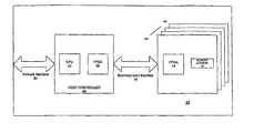
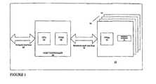
- FIG. 1depicts a block schematic diagram of a system containing a programmable device that undergoes programming through a host controller in accordance with an illustrative embodiment of the present principles
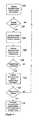
- FIG. 2depicts a flowchart showing the steps of a method for programming the programmable device of FIG. 1 in accordance with the present principles.
- FPGAField Programmable gate Array
- FIG. 1comprises a system 10 that includes at least one, and preferably a plurality of modules 12 1 - 12 n that perform various signal processing functions.
- the modulescould process one or more of video, audio, time code and ancillary information.
- At least one module, such as module 12 1has at least one programmable device, such as a FPGA 14 , and can include other devices, such as memory element 16 for example, which as discussed above can undergo programming in accordance with the present principles.
- the FPGA 14can read the memory element 16 to alter the FPGA behavior.
- the FPGA 14has one or more configurable logic blocks (not shown) which can be set and thereafter reset in response to programming of the FPGA though an interface.
- fault tolerant programming of the FPGA 14 on the module 12 1typically required that a technician travel to the location of the system 10 to gain physical access to the module. Often, the technician needed special equipment for this task, making such re-programming costly and time-consuming.
- Boundary scan interface 18between the electronic system 10 and a host controller 20 .
- JTAGJoint Test Action Group
- one or more pins of an integrated circuitto a Boundary scan interface which provides a mechanism for connecting a signal from an external source to such pins circuits.
- the pins of the integrated circuit(s) coupled to the Boundary scan interfacehave associated Boundary scan cells within the respective integrated circuit(s) that are coupled in a serial chain so that a signal launched into one pin gets serially shifted through the chain and out through another pin.
- a given signal launched into a particular integrated circuit, or a combination of interconnected circuits, via the Boundary scan interfacewill yield a signal indicative of the circuit or combination of circuits.
- the host controller 20undertakes the programming of the FPGA 14 on the module 12 1 (as well as the programming of other programmable devices on other modules if appropriate) under control of a central processing unit (CPU) 22 .
- the CPU 24 of the host controller 20can receive both command and program information through a network interface 24 .
- the CPU 22will first identify the module and thereafter supply programming to the module 12 1 corresponding to the identification for receipt by the FPGA 14 or by the memory element 16 on that module.
- the CPU 22could accomplish such programming following module identification by first programming a FPGA 26 associated with the host controller 20 , and then replicating that program to the FPGA 14 or memory element 16 on the module 12 1 .
- Other programmable devices on other modulescould undergo programming in the same manner. Rather than make use of the FPGA 26 on the host controller 20 to store programming information for later transfer to a programmable device, such as FPGA 14 , on a module such as module 12 1 , the host controller could employ another type of memory for that purpose.
- the host controller 20 identification of the FPGA 14 identificationinvolves utilization of a JTAG idcode assigned to the FPGA 14 upon its manufacture.
- the host controller 20makes use of the JTAG idcode and the assigned I/O pins of the FPGA to uniquely identify the target program for the module.
- This methodallows for multiple modules that use the same type of FPGAs (those having the same idcode) to have different programs based on the additional configuration of the assigned FPGA I/O pins.
- the host controller 20can make the proper identification of the target program, thereby allowing multiple modules using the same or different types of FPGAs to communicate with a single host controller to obtain the correct target program code.
- the modulestypically connect with each other through their Boundary scan interfaces in one or more JTAG chains.
- FIG. 2depicts in flow chart form the steps of an exemplary method employed by the host controller 20 of FIG. 1 to program a programmable device (e.g., FPGA 14 ) on one or more of the modules 12 1 - 12 n of FIG. 1 .
- the methodcommences upon execution of step 100 of FIG. 2 during which the host controller 20 initializes Boundary scan-based module identification.
- the host controller 20launches a signal, typically in the form of a vector containing a plurality of known values, into the Boundary scan interface 18 of FIG. 1 , causing the module 12 1 of FIG. 1 to generate a particular response based on the nature of the module.
- the host controller 20then analyzes the response, taking into account the JTAG idcode and FPGA I/O pin assignments as discussed previously. By launching a signal to the module, and then analyzing the response, the host controller 20 thus serves to query the module to ascertain its identity. Following step 100 , the host controller 20 determines whether it can identify the module based on the response received from the module during step 102 of FIG. 2 . If the host controller 20 of FIG. 1 cannot successfully identify the module, step 100 gets repeated until successful module identification occurs. Note that a module, such as module 12 1 could contain a single programmable device, such as FPGA 14 . Thus, by initiating querying of such a module 12 1 during step 100 , the host controller effectively queries the programmable device.
- the host controller 20Upon successful module identification, the host controller 20 will retrieve one or more specific program files for the corresponding identified module during step 104 .
- the host controller 20 of FIG. 1typically retrieves the corresponding module-specific program file(s) from an external source (not shown) through the network interface 24 of FIG. 1 .
- the host controller 20could retrieve the corresponding module-specific program files from a local memory (not shown).
- the host controllerinitializes Boundary-scan-based module programming during step 106 .
- the host controller 20downloads the module-specific program file(s) through the Boundary-scan interface 18 of FIG. 1 to program the programmable logic blocks within the FPGA 14 in the given module. (In the event the programmable device on the module operates in a different way, the host controller 20 will download the module-specific program file(s) in a manner to reprogram that device).
- step 108the host controller 20 checks whether programming has been completed. If not, program execution branches back to step 100 and those following it. Returning to the first step (step 100 ) in the programming process, rather than repeating step 106 helps to make the programming process fault tolerant. Simply repeating step 106 upon a determination of incomplete programming during step 108 could run the risk that programming ultimately performed could result in flaws. In contrast, restarting the programming process by returning to step 100 upon a determination of incomplete programming during step 108 greatly reduces the likelihood of programming flaws.
- step 110next undergoes execution during which the host controller 20 of FIG. 1 initializes Boundary-scan-based programming verification.
- the host controller 20determines whether programming verification has occurred successfully. If not, then step 100 and those following it get re-executed to assure fault tolerance in the same manner as discussed above.
- the host controller 20 of FIG. 1terminates the boundary-scan-based module identification and programming process during step 114 .
Landscapes
- Engineering & Computer Science (AREA)
- Computer Hardware Design (AREA)
- Physics & Mathematics (AREA)
- Theoretical Computer Science (AREA)
- Evolutionary Computation (AREA)
- Geometry (AREA)
- General Engineering & Computer Science (AREA)
- General Physics & Mathematics (AREA)
- Stored Programmes (AREA)
- Logic Circuits (AREA)
- Semiconductor Integrated Circuits (AREA)
- Design And Manufacture Of Integrated Circuits (AREA)
Abstract
Description
Claims (16)
Priority Applications (1)
| Application Number | Priority Date | Filing Date | Title |
|---|---|---|---|
| US12/311,877US8225153B2 (en) | 2006-10-16 | 2006-11-21 | Tolerant in-system programming of field programmable gate arrays (FPGAs) |
Applications Claiming Priority (3)
| Application Number | Priority Date | Filing Date | Title |
|---|---|---|---|
| US85195406P | 2006-10-16 | 2006-10-16 | |
| PCT/US2006/044951WO2008048297A1 (en) | 2006-10-16 | 2006-11-21 | Tolerant in-system programming of field programmable gate arrays (epgas) |
| US12/311,877US8225153B2 (en) | 2006-10-16 | 2006-11-21 | Tolerant in-system programming of field programmable gate arrays (FPGAs) |
Publications (2)
| Publication Number | Publication Date |
|---|---|
| US20100281318A1 US20100281318A1 (en) | 2010-11-04 |
| US8225153B2true US8225153B2 (en) | 2012-07-17 |
Family
ID=38016426
Family Applications (1)
| Application Number | Title | Priority Date | Filing Date |
|---|---|---|---|
| US12/311,877Expired - Fee RelatedUS8225153B2 (en) | 2006-10-16 | 2006-11-21 | Tolerant in-system programming of field programmable gate arrays (FPGAs) |
Country Status (6)
| Country | Link |
|---|---|
| US (1) | US8225153B2 (en) |
| EP (1) | EP2074537A1 (en) |
| JP (1) | JP2010507227A (en) |
| CN (1) | CN101529426A (en) |
| CA (1) | CA2666391A1 (en) |
| WO (1) | WO2008048297A1 (en) |
Cited By (5)
| Publication number | Priority date | Publication date | Assignee | Title |
|---|---|---|---|---|
| US20130346814A1 (en)* | 2012-06-21 | 2013-12-26 | Timothy Zadigian | Jtag-based programming and debug |
| US9026688B2 (en) | 2012-06-21 | 2015-05-05 | Breakingpoint Systems, Inc. | Systems and methods for programming configurable logic devices via USB |
| US10404470B2 (en) | 2017-01-13 | 2019-09-03 | Microsoft Technology Licensing, Llc | Signature verification of field-programmable gate array programs |
| US10540506B2 (en) | 2017-01-12 | 2020-01-21 | Microsoft Technology Licensing, Llc | Field-programmable gate array virtualization |
| US11520892B2 (en)* | 2019-01-29 | 2022-12-06 | Robert Bosch Gmbh | Integrated circuit and embedded system including such an integrated circuit with bootstrap configuration for attack prevention |
Families Citing this family (4)
| Publication number | Priority date | Publication date | Assignee | Title |
|---|---|---|---|---|
| CA3228818A1 (en)* | 2009-01-15 | 2010-07-22 | Electronic Warfare Associates, Inc. | Systems and methods of implementing remote boundary scan features |
| TWI557746B (en) | 2011-05-10 | 2016-11-11 | 電子戰協會公司 | Systems and methods of implementing content validation of microcomputer based circuits |
| TWI546692B (en) | 2011-10-27 | 2016-08-21 | 電子戰協會公司 | Systems and methods of device authentication including features of circuit testing and verification in connection with known board information |
| US10096380B1 (en)* | 2017-08-31 | 2018-10-09 | Micron Technology, Inc. | Erase page check |
Citations (25)
| Publication number | Priority date | Publication date | Assignee | Title |
|---|---|---|---|---|
| US5457408A (en) | 1994-11-23 | 1995-10-10 | At&T Corp. | Method and apparatus for verifying whether a bitstream received by a field programmable gate array (FPGA) is intended for that FPGA |
| EP0755017A2 (en) | 1995-07-21 | 1997-01-22 | Lattice Semiconductor Corporation | Method for simultaneous programming of in-system programmable integrated circuits |
| TW298619B (en) | 1995-12-12 | 1997-02-21 | Ibm | Testable programmable gate array and associated LSSD/deterministic test methodology |
| US5999014A (en)* | 1997-09-17 | 1999-12-07 | Xilinx, Inc. | Method for concurrently programming or accessing a plurality of in-system-programmable logic devices |
| US6356107B1 (en) | 1998-05-21 | 2002-03-12 | Lattice Semiconductor Corporation | Method and structure dynamic in-system programming |
| US20020170000A1 (en) | 2001-05-09 | 2002-11-14 | Emanuel Gorodetsky | Test and on-board programming station |
| US20020199110A1 (en)* | 2001-06-13 | 2002-12-26 | Algotronix Ltd. | Method of protecting intellectual property cores on field programmable gate array |
| US20030023771A1 (en) | 2001-07-30 | 2003-01-30 | Erickson Michael John | Method for accessing scan chains and updating EEPROM-resident FPGA code through a system mangement processor and JTAG bus |
| US6539510B1 (en) | 1997-08-12 | 2003-03-25 | Xilinx, Inc. | Interface board for receiving modular interface cards |
| KR20030058385A (en) | 2001-12-31 | 2003-07-07 | 대우종합기계 주식회사 | Apparatus for preventing shock by quick operation |
| US20030187629A1 (en) | 2002-03-28 | 2003-10-02 | Lucent Technologies Inc. | Concurrent in-system programming of programmable devices |
| US20040001432A1 (en) | 2002-06-28 | 2004-01-01 | Douglas Albert Wescott | Embedding a JTAG host controller into an FPGA design |
| US6714040B1 (en) | 2002-06-03 | 2004-03-30 | Xilinx, Inc. | Automated boundary-scan chain composition method using a device database and access mechanism for storing and retrieving situation-dependent operation options |
| US20050050393A1 (en) | 2003-08-26 | 2005-03-03 | Chakraborty Tapan J. | Fault injection method and system |
| US20050094466A1 (en)* | 2003-10-31 | 2005-05-05 | The Regents Of The University Of California | List mode multichannel analyzer |
| US6898776B1 (en)* | 2002-06-03 | 2005-05-24 | Xilinx, Inc. | Method for concurrently programming a plurality of in-system-programmable logic devices by grouping devices to achieve minimum configuration time |
| US6948147B1 (en) | 2003-04-03 | 2005-09-20 | Xilinx, Inc. | Method and apparatus for configuring a programmable logic device using a master JTAG port |
| US20050240892A1 (en) | 2002-12-31 | 2005-10-27 | Lsi Logic Corporation | Suite of tools to design integrated circuits |
| US20050262396A1 (en)* | 2004-04-26 | 2005-11-24 | Agilent Technologies, Inc | Apparatus and method for automated test setup |
| US20060190905A1 (en) | 2005-02-24 | 2006-08-24 | Nick Martin | System for designing re-programmable digital hardware platforms |
| US20060277346A1 (en)* | 2003-10-06 | 2006-12-07 | David Doak | Port adapter for high-bandwidth bus |
| US7155711B2 (en)* | 1999-12-10 | 2006-12-26 | Sedna Patent Services, Llc | Method and apparatus providing remote reprogramming of programmable logic devices using embedded JTAG physical layer and protocol |
| TWI298619B (en) | 2005-08-26 | 2008-07-01 | Hon Hai Prec Ind Co Ltd | Electronic devices and heat sink for preventing electromagnetic interference thereof |
| US7454556B1 (en)* | 2005-02-02 | 2008-11-18 | Xilinx, Inc. | Method to program non-JTAG attached devices or memories using a PLD and its associated JTAG interface |
| US7505331B1 (en)* | 2005-11-23 | 2009-03-17 | Altera Corporation | Programmable logic device with differential communications support |
Family Cites Families (1)
| Publication number | Priority date | Publication date | Assignee | Title |
|---|---|---|---|---|
| JP2000311943A (en)* | 1999-04-27 | 2000-11-07 | Mitsubishi Electric Corp | Semiconductor device |
- 2006
- 2006-11-21CACA002666391Apatent/CA2666391A1/ennot_activeAbandoned
- 2006-11-21WOPCT/US2006/044951patent/WO2008048297A1/enactiveApplication Filing
- 2006-11-21JPJP2009532337Apatent/JP2010507227A/enactivePending
- 2006-11-21CNCNA2006800561315Apatent/CN101529426A/enactivePending
- 2006-11-21EPEP06838105Apatent/EP2074537A1/ennot_activeWithdrawn
- 2006-11-21USUS12/311,877patent/US8225153B2/ennot_activeExpired - Fee Related
Patent Citations (29)
| Publication number | Priority date | Publication date | Assignee | Title |
|---|---|---|---|---|
| JPH08237110A (en) | 1994-11-23 | 1996-09-13 | At & T Corp | Field programmable gate array and its method of application |
| US5457408A (en) | 1994-11-23 | 1995-10-10 | At&T Corp. | Method and apparatus for verifying whether a bitstream received by a field programmable gate array (FPGA) is intended for that FPGA |
| EP0755017A2 (en) | 1995-07-21 | 1997-01-22 | Lattice Semiconductor Corporation | Method for simultaneous programming of in-system programmable integrated circuits |
| TW298619B (en) | 1995-12-12 | 1997-02-21 | Ibm | Testable programmable gate array and associated LSSD/deterministic test methodology |
| US5867507A (en) | 1995-12-12 | 1999-02-02 | International Business Machines Corporation | Testable programmable gate array and associated LSSD/deterministic test methodology |
| US6539510B1 (en) | 1997-08-12 | 2003-03-25 | Xilinx, Inc. | Interface board for receiving modular interface cards |
| US5999014A (en)* | 1997-09-17 | 1999-12-07 | Xilinx, Inc. | Method for concurrently programming or accessing a plurality of in-system-programmable logic devices |
| US6356107B1 (en) | 1998-05-21 | 2002-03-12 | Lattice Semiconductor Corporation | Method and structure dynamic in-system programming |
| US7155711B2 (en)* | 1999-12-10 | 2006-12-26 | Sedna Patent Services, Llc | Method and apparatus providing remote reprogramming of programmable logic devices using embedded JTAG physical layer and protocol |
| US20020170000A1 (en) | 2001-05-09 | 2002-11-14 | Emanuel Gorodetsky | Test and on-board programming station |
| US20020199110A1 (en)* | 2001-06-13 | 2002-12-26 | Algotronix Ltd. | Method of protecting intellectual property cores on field programmable gate array |
| US20030023771A1 (en) | 2001-07-30 | 2003-01-30 | Erickson Michael John | Method for accessing scan chains and updating EEPROM-resident FPGA code through a system mangement processor and JTAG bus |
| KR20030058385A (en) | 2001-12-31 | 2003-07-07 | 대우종합기계 주식회사 | Apparatus for preventing shock by quick operation |
| US20030187629A1 (en) | 2002-03-28 | 2003-10-02 | Lucent Technologies Inc. | Concurrent in-system programming of programmable devices |
| US6714040B1 (en) | 2002-06-03 | 2004-03-30 | Xilinx, Inc. | Automated boundary-scan chain composition method using a device database and access mechanism for storing and retrieving situation-dependent operation options |
| US6898776B1 (en)* | 2002-06-03 | 2005-05-24 | Xilinx, Inc. | Method for concurrently programming a plurality of in-system-programmable logic devices by grouping devices to achieve minimum configuration time |
| US7023239B1 (en)* | 2002-06-03 | 2006-04-04 | Xilinx, Inc. | Automated boundary-scan chain composition method using a device database and access mechanism for storing and retrieving situation-dependent operation options |
| US20040001432A1 (en) | 2002-06-28 | 2004-01-01 | Douglas Albert Wescott | Embedding a JTAG host controller into an FPGA design |
| US20050240892A1 (en) | 2002-12-31 | 2005-10-27 | Lsi Logic Corporation | Suite of tools to design integrated circuits |
| US6948147B1 (en) | 2003-04-03 | 2005-09-20 | Xilinx, Inc. | Method and apparatus for configuring a programmable logic device using a master JTAG port |
| US20050050393A1 (en) | 2003-08-26 | 2005-03-03 | Chakraborty Tapan J. | Fault injection method and system |
| US20060277346A1 (en)* | 2003-10-06 | 2006-12-07 | David Doak | Port adapter for high-bandwidth bus |
| US20050094466A1 (en)* | 2003-10-31 | 2005-05-05 | The Regents Of The University Of California | List mode multichannel analyzer |
| US20050262396A1 (en)* | 2004-04-26 | 2005-11-24 | Agilent Technologies, Inc | Apparatus and method for automated test setup |
| US7454556B1 (en)* | 2005-02-02 | 2008-11-18 | Xilinx, Inc. | Method to program non-JTAG attached devices or memories using a PLD and its associated JTAG interface |
| US20060190905A1 (en) | 2005-02-24 | 2006-08-24 | Nick Martin | System for designing re-programmable digital hardware platforms |
| TWI298619B (en) | 2005-08-26 | 2008-07-01 | Hon Hai Prec Ind Co Ltd | Electronic devices and heat sink for preventing electromagnetic interference thereof |
| US7505331B1 (en)* | 2005-11-23 | 2009-03-17 | Altera Corporation | Programmable logic device with differential communications support |
| US7958416B1 (en)* | 2005-11-23 | 2011-06-07 | Altera Corporation | Programmable logic device with differential communications support |
Non-Patent Citations (15)
| Title |
|---|
| Ahrens: "Test standard serves dual role as on-board programming solution," Field-Programmable Logic and Applications, 5th Int'l. Workshop, FPL '95 Proceedings, Oxford, UK, Aug. 29-Sep. 1, 1995, pp. 235-240 by Springer-Verlag, Berlin, Germany. |
| Aubert: "Boundary scan modification to enhance multichip module testing," IEEE Proceedings of 1992 National Aerospace and Electronics Conference, NAECON 1992, May 18-22, 1992, Dayton, OH, USA, pp. 979-984, vol. 3, published NY, NY. |
| Chakraborty et al.: "A novel fault injection method for system verification based on FPGA boundary scan architecture," IEEE Proceedings Int'l. Test Conference 2002, Baltimore, MD, USA, Oct. 7-10, 2002, pp. 923-929, published Piscataway, NJ, USA. |
| Conner, T.: "Using IEEE 1149.1 for in-system programming (ISP)," Proceedings of the Technical Program NEPCON East '97 Conference, Boston, MA, Jun. 9-12, 1997, pp. 51-54, Reed Exhibition, Norwalk, CT, USA. |
| Corelis: "Boundary-Scan Tutorial," Innovation in boundary-scan, http://www.corelis.com/products/Boundary-Scan-Tutorial.htm, pp. 1-14. |
| Gericota et al.: "Draft: an on-line fault detection method for dynamic and partially reconfigurable FPGAs," IEEE Proceedings 7th Int'l. On-Line Testing Workshop, pp. 34-36, Taormina, Italy, Jul. 9-11, 2001, published in Los Alamitos, CA, USA. |
| IEEE Computer Society: "Proceedings DELTA 2004, Second IEEE Intl. Workshop on Electronic Design, Test and Applications," Perth, WA, Australia, Jan. 28-30, 2004, published Los Alamitos, CA, USA. |
| IEEE Computer Society: "Proceedings Int'l. Test Conference 2004 (IEEE Cat. No. 04CH37586)," Charlotte, NC, USA, Oct. 26-28, 2004, published Piscataway, NJ, USA. |
| Japanese Office Action in Japanese Patent Application No. 2009-532337 mailed May 18, 2012. |
| Park et al.: "A New IEEE 1149.1 Boundary Scan Design for the Detection of Delay Defects," Dept. of Computer Science & Engineering Hanyang University, Korea, parksj@mslab.hanyang.ac.kr, 5 pages. |
| Pottinger et al.: "Using a reconfigurable field programmable gate array to demonstrate boundary scan with built in self test," IEEE Proceedings of Fifth Great Lakes Symposium on VLSI, Buffalo, NY, USA, Mar. 16-18, 1995, pp. 242-245, Los Alamitos, CA, USA. |
| Stojcev et al.: "Parity error detection in embedded computer system," 5th Int'l. Conference on Telecommunications in Modern Satellite, Cable and Broadcasting Service, TELSIKS 2001, vol. 2, pp. 445-450, Nis, Yugoslavia, Sep. 19-21, 2001, Piscataway, NJ, USA. |
| The International Search Report, dated Jun. 21, 2007. |
| Ungar et al.: "Testability beyond JTAG," EE Evaluation Engineering, vol. 44, No. 9, pp. 48-50, 52-54, Sep. 2005, Nelson Publishing, USA. |
| Wikipedia, the free encyclopedia: "Field-programmable gate array," http://en.wikipedia.org/wiki/FPGA, Oct. 17, 2006. |
Cited By (6)
| Publication number | Priority date | Publication date | Assignee | Title |
|---|---|---|---|---|
| US20130346814A1 (en)* | 2012-06-21 | 2013-12-26 | Timothy Zadigian | Jtag-based programming and debug |
| US8856600B2 (en)* | 2012-06-21 | 2014-10-07 | Breakingpoint Systems, Inc. | JTAG-based programming and debug |
| US9026688B2 (en) | 2012-06-21 | 2015-05-05 | Breakingpoint Systems, Inc. | Systems and methods for programming configurable logic devices via USB |
| US10540506B2 (en) | 2017-01-12 | 2020-01-21 | Microsoft Technology Licensing, Llc | Field-programmable gate array virtualization |
| US10404470B2 (en) | 2017-01-13 | 2019-09-03 | Microsoft Technology Licensing, Llc | Signature verification of field-programmable gate array programs |
| US11520892B2 (en)* | 2019-01-29 | 2022-12-06 | Robert Bosch Gmbh | Integrated circuit and embedded system including such an integrated circuit with bootstrap configuration for attack prevention |
Also Published As
| Publication number | Publication date |
|---|---|
| CA2666391A1 (en) | 2008-04-24 |
| EP2074537A1 (en) | 2009-07-01 |
| JP2010507227A (en) | 2010-03-04 |
| US20100281318A1 (en) | 2010-11-04 |
| WO2008048297A1 (en) | 2008-04-24 |
| CN101529426A (en) | 2009-09-09 |
Similar Documents
| Publication | Publication Date | Title |
|---|---|---|
| US8225153B2 (en) | Tolerant in-system programming of field programmable gate arrays (FPGAs) | |
| US7020598B1 (en) | Network based diagnostic system and method for software reconfigurable systems | |
| US5790771A (en) | Apparatus and method for configuring a reconfigurable electronic system having defective resources | |
| US9121892B2 (en) | Semiconductor circuit and methodology for in-system scan testing | |
| CN106771991B (en) | Automatic testing method applied to antifuse Field Programmable Gate Array (FPGA) before programming | |
| CN101329621B (en) | control device | |
| US10371751B2 (en) | Circuit and method for diagnosing scan chain failures | |
| CN102043747B (en) | Method for downloading field programmable gate array (FPGA) logic codes under joint test action group (JTAG) download mode | |
| US4581738A (en) | Test and maintenance method and apparatus for a data processing system | |
| JP2003140917A (en) | Method and device for performing in-system programming of programmable logic device on multiple boards through common connection point | |
| US8825934B2 (en) | Gang programming of devices | |
| CN105093096A (en) | Testing device for FPGA (Field-Programmable Gate Array) | |
| US9026873B2 (en) | Method and apparatus for securing configuration scan chains of a programmable device | |
| US7685327B1 (en) | Identification of multi-device systems | |
| US7024327B1 (en) | Techniques for automatically generating tests for programmable circuits | |
| CN116090380B (en) | Automatic method and device for verifying digital integrated circuit, storage medium and terminal | |
| US6714040B1 (en) | Automated boundary-scan chain composition method using a device database and access mechanism for storing and retrieving situation-dependent operation options | |
| US20050171756A1 (en) | Method and apparatus for the automatic correction of faulty wires in a logic simulation hardware emulator / accelerator | |
| US4625312A (en) | Test and maintenance method and apparatus for investigation of intermittent faults in a data processing system | |
| US6671564B1 (en) | Portable programming system and control method therefor | |
| US6772381B1 (en) | Programmable logic device verification system and method | |
| US7506210B1 (en) | Method of debugging PLD configuration using boundary scan | |
| US6778933B2 (en) | Processing semiconductor devices having some defective input-output pins | |
| US7299430B1 (en) | Reducing design execution run time bit stream size for device testing | |
| CN118585386B (en) | Method, device, equipment and storage medium for mass production test of FPGA interconnection resources |
Legal Events
| Date | Code | Title | Description |
|---|---|---|---|
| AS | Assignment | Owner name:THOMSON LICENSING, FRANCE Free format text:ASSIGNMENT OF ASSIGNORS INTEREST;ASSIGNORS:REDONDO, RANDALL G.;RICHARD, THOMAS MICHAEL;REEL/FRAME:022578/0819 Effective date:20061024 | |
| AS | Assignment | Owner name:GVBB HOLDINGS S.A.R.L., LUXEMBOURG Free format text:ASSIGNMENT OF ASSIGNORS INTEREST;ASSIGNOR:THOMSON LICENSING;REEL/FRAME:026028/0071 Effective date:20101231 | |
| ZAAA | Notice of allowance and fees due | Free format text:ORIGINAL CODE: NOA | |
| ZAAB | Notice of allowance mailed | Free format text:ORIGINAL CODE: MN/=. | |
| STCF | Information on status: patent grant | Free format text:PATENTED CASE | |
| FPAY | Fee payment | Year of fee payment:4 | |
| MAFP | Maintenance fee payment | Free format text:PAYMENT OF MAINTENANCE FEE, 8TH YEAR, LARGE ENTITY (ORIGINAL EVENT CODE: M1552); ENTITY STATUS OF PATENT OWNER: LARGE ENTITY Year of fee payment:8 | |
| AS | Assignment | Owner name:GRASS VALLEY CANADA, QUEBEC Free format text:ASSIGNMENT OF ASSIGNORS INTEREST;ASSIGNOR:GVBB HOLDINGS S.A.R.L.;REEL/FRAME:056100/0612 Effective date:20210122 | |
| FEPP | Fee payment procedure | Free format text:MAINTENANCE FEE REMINDER MAILED (ORIGINAL EVENT CODE: REM.); ENTITY STATUS OF PATENT OWNER: LARGE ENTITY | |
| AS | Assignment | Owner name:MS PRIVATE CREDIT ADMINISTRATIVE SERVICES LLC, NEW YORK Free format text:SECURITY INTEREST;ASSIGNORS:GRASS VALLEY CANADA;GRASS VALLEY LIMITED;REEL/FRAME:066850/0869 Effective date:20240320 | |
| LAPS | Lapse for failure to pay maintenance fees | Free format text:PATENT EXPIRED FOR FAILURE TO PAY MAINTENANCE FEES (ORIGINAL EVENT CODE: EXP.); ENTITY STATUS OF PATENT OWNER: LARGE ENTITY | |
| STCH | Information on status: patent discontinuation | Free format text:PATENT EXPIRED DUE TO NONPAYMENT OF MAINTENANCE FEES UNDER 37 CFR 1.362 | |
| FP | Lapsed due to failure to pay maintenance fee | Effective date:20240717 |