US8222936B2 - Phase and frequency detector with output proportional to frequency difference - Google Patents
Phase and frequency detector with output proportional to frequency differenceDownload PDFInfo
- Publication number
- US8222936B2 US8222936B2US12/813,828US81382810AUS8222936B2US 8222936 B2US8222936 B2US 8222936B2US 81382810 AUS81382810 AUS 81382810AUS 8222936 B2US8222936 B2US 8222936B2
- Authority
- US
- United States
- Prior art keywords
- signal
- frequency
- clock
- circuit
- phase
- Prior art date
- Legal status (The legal status is an assumption and is not a legal conclusion. Google has not performed a legal analysis and makes no representation as to the accuracy of the status listed.)
- Active, expires
Links
- 238000000034methodMethods0.000claimsabstractdescription13
- 230000004044responseEffects0.000claimsabstractdescription8
- 230000000630rising effectEffects0.000claimsdescription13
- 230000000737periodic effectEffects0.000claimsdescription4
- 238000010586diagramMethods0.000description14
- 238000004590computer programMethods0.000description9
- 230000006870functionEffects0.000description9
- 238000001514detection methodMethods0.000description7
- 238000012545processingMethods0.000description5
- 239000003990capacitorSubstances0.000description3
- 230000003287optical effectEffects0.000description3
- 238000004088simulationMethods0.000description3
- 230000008901benefitEffects0.000description2
- 238000003708edge detectionMethods0.000description2
- 230000007246mechanismEffects0.000description2
- 239000013307optical fiberSubstances0.000description2
- 230000008569processEffects0.000description2
- 230000000644propagated effectEffects0.000description2
- 230000007704transitionEffects0.000description2
- 230000015572biosynthetic processEffects0.000description1
- 230000008859changeEffects0.000description1
- 239000013078crystalSubstances0.000description1
- 238000013461designMethods0.000description1
- 230000007717exclusionEffects0.000description1
- 230000009191jumpingEffects0.000description1
- 238000004519manufacturing processMethods0.000description1
- 238000012986modificationMethods0.000description1
- 230000004048modificationEffects0.000description1
- 230000010355oscillationEffects0.000description1
- 230000037452primingEffects0.000description1
- 230000000135prohibitive effectEffects0.000description1
- 230000001105regulatory effectEffects0.000description1
- 239000004065semiconductorSubstances0.000description1
- 230000001360synchronised effectEffects0.000description1
- 238000003786synthesis reactionMethods0.000description1
- 238000012546transferMethods0.000description1
Images


Classifications
- H—ELECTRICITY
- H03—ELECTRONIC CIRCUITRY
- H03L—AUTOMATIC CONTROL, STARTING, SYNCHRONISATION OR STABILISATION OF GENERATORS OF ELECTRONIC OSCILLATIONS OR PULSES
- H03L7/00—Automatic control of frequency or phase; Synchronisation
- H03L7/06—Automatic control of frequency or phase; Synchronisation using a reference signal applied to a frequency- or phase-locked loop
- H03L7/08—Details of the phase-locked loop
- H03L7/085—Details of the phase-locked loop concerning mainly the frequency- or phase-detection arrangement including the filtering or amplification of its output signal
- H03L7/089—Details of the phase-locked loop concerning mainly the frequency- or phase-detection arrangement including the filtering or amplification of its output signal the phase or frequency detector generating up-down pulses
- H—ELECTRICITY
- H03—ELECTRONIC CIRCUITRY
- H03L—AUTOMATIC CONTROL, STARTING, SYNCHRONISATION OR STABILISATION OF GENERATORS OF ELECTRONIC OSCILLATIONS OR PULSES
- H03L7/00—Automatic control of frequency or phase; Synchronisation
- H03L7/06—Automatic control of frequency or phase; Synchronisation using a reference signal applied to a frequency- or phase-locked loop
- H03L7/08—Details of the phase-locked loop
- H03L7/085—Details of the phase-locked loop concerning mainly the frequency- or phase-detection arrangement including the filtering or amplification of its output signal
- H03L7/093—Details of the phase-locked loop concerning mainly the frequency- or phase-detection arrangement including the filtering or amplification of its output signal using special filtering or amplification characteristics in the loop
- H—ELECTRICITY
- H03—ELECTRONIC CIRCUITRY
- H03L—AUTOMATIC CONTROL, STARTING, SYNCHRONISATION OR STABILISATION OF GENERATORS OF ELECTRONIC OSCILLATIONS OR PULSES
- H03L7/00—Automatic control of frequency or phase; Synchronisation
- H03L7/06—Automatic control of frequency or phase; Synchronisation using a reference signal applied to a frequency- or phase-locked loop
- H03L7/08—Details of the phase-locked loop
- H03L7/10—Details of the phase-locked loop for assuring initial synchronisation or for broadening the capture range
- H03L7/107—Details of the phase-locked loop for assuring initial synchronisation or for broadening the capture range using a variable transfer function for the loop, e.g. low pass filter having a variable bandwidth
- H03L7/1077—Details of the phase-locked loop for assuring initial synchronisation or for broadening the capture range using a variable transfer function for the loop, e.g. low pass filter having a variable bandwidth by changing characteristics of the phase or frequency detection means
- H—ELECTRICITY
- H03—ELECTRONIC CIRCUITRY
- H03L—AUTOMATIC CONTROL, STARTING, SYNCHRONISATION OR STABILISATION OF GENERATORS OF ELECTRONIC OSCILLATIONS OR PULSES
- H03L7/00—Automatic control of frequency or phase; Synchronisation
- H03L7/06—Automatic control of frequency or phase; Synchronisation using a reference signal applied to a frequency- or phase-locked loop
- H03L7/16—Indirect frequency synthesis, i.e. generating a desired one of a number of predetermined frequencies using a frequency- or phase-locked loop
- H03L7/18—Indirect frequency synthesis, i.e. generating a desired one of a number of predetermined frequencies using a frequency- or phase-locked loop using a frequency divider or counter in the loop
- H03L7/197—Indirect frequency synthesis, i.e. generating a desired one of a number of predetermined frequencies using a frequency- or phase-locked loop using a frequency divider or counter in the loop a time difference being used for locking the loop, the counter counting between numbers which are variable in time or the frequency divider dividing by a factor variable in time, e.g. for obtaining fractional frequency division
- H03L7/1974—Indirect frequency synthesis, i.e. generating a desired one of a number of predetermined frequencies using a frequency- or phase-locked loop using a frequency divider or counter in the loop a time difference being used for locking the loop, the counter counting between numbers which are variable in time or the frequency divider dividing by a factor variable in time, e.g. for obtaining fractional frequency division for fractional frequency division
- H03L7/1976—Indirect frequency synthesis, i.e. generating a desired one of a number of predetermined frequencies using a frequency- or phase-locked loop using a frequency divider or counter in the loop a time difference being used for locking the loop, the counter counting between numbers which are variable in time or the frequency divider dividing by a factor variable in time, e.g. for obtaining fractional frequency division for fractional frequency division using a phase accumulator for controlling the counter or frequency divider
Definitions
- the present inventionrelates generally to phase and frequency detectors and, more specifically, to phase and frequency detectors which generate an output signal proportional to a frequency difference between two input signals.
- phase detectoris a device that measures the phase difference between two periodic input signals of the same frequency.
- a bang-bang phase detectoris a variant of the phase detector, where the output of the detector merely indicates which of the two input signals arrived earlier in time.
- phase and frequency detectoris a device that measures the phase difference between two periodic input signals when the two input signal are not of the same frequency.
- phase detectors and PFDsare typically used in phase locked loops (PLL) or delay locked loops (DLL) to generate an error signal that is used by a filter inside a loop.
- PLLphase locked loops
- DLLdelay locked loops
- Principles of the inventionprovide phase and frequency detectors and techniques for generating an output signal proportional to a frequency difference between two input signals.
- apparatuscomprises a first circuit for receiving first and second clock signals and for generating at least one signal indicative of a phase difference between the first and second clock signals.
- the apparatusalso comprises a second circuit for receiving the at least one signal generated by the first circuit and, in response to the at least one received signal, generating at least one output signal, wherein a frequency associated with the at least one output signal is proportional to a frequency difference between the first and second clock signals.
- FIG. 1illustrates a phase locked loop according to an embodiment of the invention.
- FIG. 2Aillustrates a frequency-proportional detector according to an embodiment of the invention.
- FIG. 2Billustrates a timing diagram for the detector of FIG. 2A .
- FIG. 3Aillustrates a frequency-proportional detector according to another embodiment of the invention.
- FIG. 3Billustrates a timing diagram for the detector of FIG. 3A .
- FIG. 4illustrates a phase locked loop according to another embodiment of the invention.
- FIG. 5illustrates a phase locked loop according to yet another embodiment of the invention.
- FIG. 6illustrates a simulation result associated with a phase locked loop according to an embodiment of the invention.
- FIG. 7illustrates a frequency generator according to an embodiment of the invention.
- FIG. 8illustrates a phase and frequency detector according to an embodiment of the invention.
- FIG. 9illustrates a multiplier filter according to an embodiment of the invention.
- phase locked loopPLL
- phase and frequency detection principles of the inventioncan be applied to other suitable applications.
- phase and frequency detection principles of the inventionmay be implemented in a wide variety of operating environments.
- phase and frequency detection principles of the inventionmay be implemented in a PLL used in a multi-core processor device. That is, it is realized that while modern microprocessors have the ability to trade-off power and performance by changing their clock frequency under software control, existing mechanisms for doing so in fine frequency increments, and while user code is running on the processor, tend to use a prohibitive amount of integrated circuit space, and are limited in the rate at which the frequency can change.
- use of the phase and frequency detection principles of the invention in a PLL applicationpermit for a mechanism that can provide a variable frequency to each core of a multi-core processor in an effective manner.
- the phase and frequency detection principles of the inventionmay be applied to operating environments other than microprocessors.
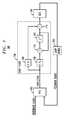
- FIG. 1illustrates a PLL application of a phase and frequency detector (PFDs).
- a loop circuit 100comprises a PFD 102 , a loop filter 104 , a digitally-controlled oscillator (DCO) 116 and a loop divider 118 .
- the loop filter 104comprises a first gain constant (k 1 ) multiplier 106 , a second gain constant (k 2 ) multiplier 108 , a first adder 110 and a unit delay element 112 (forming an integrator), and a second adder 114 .
- the PFD 102compares a reference clock signal and a feedback clock signal and produces an error signal which is proportional to the phase difference between the two input clock signals.
- the phase difference associated with the error signalis indicative of which input signal is ahead in phase (early) or behind in phase (late) with respect to the other input signal.
- the detectoroperates as a bang-bang type detector.
- the error signalis then input to the loop filter 104 whose output then drives DCO 116 .
- DCO 116generates an output clock signal at a particular frequency.
- the output clock signalis fed through the loop divider 118 generating the feedback clock signal (and forming a negative feedback loop). If the output frequency drifts, the error signal will increase, driving the DCO frequency in the opposite direction so as to reduce the error.
- the output signal from DCOis locked to the frequency of the reference clock signal.
- This reference clock signalcan be derived from a crystal oscillator, which tends to be stable in frequency.
- the loop filter 104operates as follows.
- the phase detector output signal (phase error)is multiplied by the first gain constant k 1 , which is known as the proportional gain constant.
- the result of the multiplicationis fed into the second adder 114 .
- the phase detector output signal (phase error)is also multiplied by the second gain constant k 2 , which is known as the integral gain constant.
- the result of this second multiplicationis fed into an integrator comprising the first adder 110 and a unit delay 112 (e.g., register).
- the output signal of the integratoris fed into the second adder 114 .
- the output of the second adder 114(and thus the loop filter 104 ) is the sum of the product of the proportional gain constant and the phase error computed in the multiplier 106 and the output of the integrator.
- Illustrative principles of the inventionaddress and solve this problem, as well as other problems. It is to be appreciated that while illustrative embodiments described below are implemented in terms of a bang-bang type PFD, the inventive principles can be applied in a straightforward manner to a linear type PFD.
- the phase and frequency detection principles of the inventiongenerate a signal that is proportional to the difference in frequency between the reference clock and feedback clock.
- An example of a circuit for generating the signal proportional to the difference in frequency between the reference clock and feedback clockis shown in FIG. 2A .
- the frequency-proportional detector circuit 200 in FIG. 2Acomprises a first edge-detector latch (DQ flip-flop) 202 , a second edge-detector latch (DQ flip-flop) 204 , a first output latch (DQ flip-flop) 206 , a second output latch (DQ flip-flop) 208 and an AND gate 210 .
- the function of the AND gatecan alternatively be provided by a C-element (a Muller C-gate).
- clock signals Clk_A and Clk_Barrive at the edge-detector latches 202 and 204 , respectively.
- the edge-detector latchesmay be implemented as a traditional bang-bang PFD or as a proportional PFD. That is, in a bang-bang implementation, the edge-detector latches 202 and 204 generate logic pulses (based on the phase error between the two input clock signals) with a fixed charge; while in a proportional implementation, the charges of the logic pulses are in proportion to the phase error detected.
- the AND gateclears the DQ flip-flops based on the state of the Q outputs.
- the outputs of the edge-detector latches, Edge_A and Edge_Bare then resampled by the two output latches 206 and 208 to generate signals Clk_A Faster and Clk_B Faster, respectively.
- both of these signalswill be a logic-low level, as Edge_A and Edge_B are a logic-low level before the respective clock arrives.
- a rising edge in Clk_Awill find Edge_A at a logic-high level when Clk_A gains a cycle relative to Clk_B (no reset pulse gets generated in between two Clk_A transitions).
- Clk_A Fasterwill be a logic-high level on every Clk_A rising edge that Clk_A gains a cycle with respect to Clk_B.
- Clk_B Fasteri.e., Clk_B Faster will be a logic-high level on every Clk_B rising edge that Clk_B gains a cycle with respect to Clk_A. Because a pulse is generated every time that a cycle is gained, at constant Clk_A and Clk_B frequencies, the frequency of the “Faster” pulses (outputs of latches 206 and 208 ) will be proportional to the difference between the frequencies of Clk_A and Clk_B.
- An exemplary timing diagram for the frequency-proportional detector circuit 200is shown in FIG. 2B .
- FIG. 4shows an illustrative embodiment of a PLL with a loop filter designed to take advantage of the “Faster” signals coming from the PFD (in this figure, marked as “Fast” and “Slow”).
- the loop circuit 400comprises a PFD 402 , a loop filter 404 , a digitally-controlled oscillator (DCO) 416 and a loop divider 418 .
- the loop filter 404comprises a first gain constant (k 1 ) multiplier 406 , a second gain constant (k 2 ) multiplier 408 , a third gain constant (k 3 ) multiplier 409 , a first adder 410 and a unit delay element 412 (forming an integrator), and a second adder 414 .
- the loop circuit 400operates similar to the loop circuit 100 in FIG. 1 (where like numbered components offset by 300 have similar functions as described above, i.e., 102 / 402 , 104 / 404 . . . 118 / 418 )) with the notable exception of the generation of the extra output signals by the PFD 402 , i.e., Fast/Slow. These signals correspond to the “Faster” signals described above in the context of FIG. 3A (Clk_A Faster and Clk_B Faster). These signals are accumulated in the loop filter 404 . Because the signals will never be asserted close to or in lock, parameter k 3 can be made fairly large without affecting the stability of the PLL.
- this PLL in FIG. 4will have substantially faster frequency acquisition time compared to the PLL in FIG. 1 , and can be used where a fast frequency acquisition property is required.
- the stability of the loopdepends on the ratio of k 1 to k 2 , with typical values being on the order of 10 to 100. As this number grows, the system becomes more stable, but also slower. We can use a fairly small k 1 to k 3 ratio (1 or even less), that makes the system significantly faster without making it unstable.
- the same detectorcan be used in a traditional linear analog PLL, with a linear PFD and a charge pump, as shown in FIG. 5 .
- the frequency proportional outputscan be used in the charge pump as extra inputs (Up 1 and Down 1 ), but would have a different gain from the PFD outputs (Up 2 and Down 2 ). For example, if a rising edge on Ref Clk arrives earlier than a rising edge on FB Clk, then the output of latch 502 is set to one, and the charge pump 512 increases the charge stored in capacitor 514 at a certain rate determined by the desired transfer of this circuit.
- FIG. 6a simulation is shown of a DPLL that uses phase and frequency detection principles of the invention.
- the PLLis forced to follow a very steep frequency ramp, first up in frequency and then down in frequency.
- Signals “ref_very_early” and “ref_very_late”are the signals generated in accordance with an illustrative embodiment of the invention (after synchronization to the loop filter clock). It can be seen how one of them helps the PLL follow the up ramp, while the other helps the PLL follow the down ramp. It is to be understood that signals “ref_very_early” and “ref_very_late” respectively refer to the Fast/Slow signals in FIG. 4 .
- FIG. 7shows a frequency generator 700 , which is based on an all-digital PLL 702 .
- a bang-bang, self-timed phase and frequency detector (PFD) 704compares the reference clock to the divided down feedback clock, and generates two sets of signals. One set is the usual early/late information used to keep the DPLL phase locked. The second set, faster/slower, is a pulse stream whose intensity is proportional to the frequency difference between reference and feedback clocks. This pulse stream is generated, as explained above, in accordance with an embodiment of the invention.
- PFDphase and frequency detector
- the digital loop filter 706is a programmable proportional-integral filter with a 12-bit accumulator, that is clocked by the divided down feedback clock.
- Overflows and underflows from this 12-bit accumulatorare used to increment or decrement the DCO frequency, set by the DCO control block 708 .
- Thisforces an immediate overflow or underflow condition, thus creating a high-gain path into the DCO 712 .
- the five most significant bits of the accumulatorare sent to a 2 nd order ⁇ encoder 710 running at a multiple of the loop filter frequency.
- the DCO 712is a three stage ring oscillator, each stage of the ring including multiple tri-state inverters connected in parallel. Oscillation frequency is determined by how many inverters are turned on. These inverters are placed in an array, and controlled with a row-column pseudo-thermometer code. Two extra rows of inverters are used to implement frequency dithering, a loop filter bypass of the proportional path, and start-up.
- the output of the DCOis divided down by 1, 2, or 4 by output divider 716 to generate the DPLL output clock.
- the output of the DCOis also divided down by 2, 4, or 8 (pre-scaler 718 ) before being used for all of the digital logic inside of the DPLL. Further divisions and clock phases are generated by the feedback divider 722 using “phase holds,” or clock gating signals.
- a first-order ⁇ encoder 724transforms a 14-bit frequency multiplier word into a 6-bit integer multiplier word, to implement fractional-N frequency synthesis. This 14-bit frequency multiplier is generated by the multiplier filter 726 .
- the multiplier filter 726will use both the target multiplier and slew rate to generate a frequency ramp, or use the output of the critical path monitor (CPM) filter to reach a CPM-optimized frequency.
- CPMcritical path monitor
- a key feature of the design of FIG. 7is the fast lock circuit 800 , shown in FIG. 8 , which allows the DPLL to track changes to the frequency multiplier.
- the fast lock circuit 800corresponds to PFD 702 in FIG. 7 .
- Edges on Ref Clk and FB Clkare detected by edge-detection latches 802 and 804 , respectively, and passed through a mutual exclusion circuit (mutex) 806 , to assert either Ref First or FB First, according to which edge happened first.
- the mutex 806ensures that these two signals are not simultaneously asserted.
- a self-timed set-reset latch 808stores the result of the arrival order.
- a done signalis generated by a three-input C-element 810 , resetting the edge-detection latches 802 and 804 and priming the circuit 800 for a new pair of edges.
- Signals Ref Early and FB Earlyare stable until a new edge arrives, and are sampled for use by the loop filter ( 706 in FIG. 7 ).
- the output frequency of the DPLL 702can be changed on the fly by programming a new frequency multiplier in the feedback divider (via 722 , 724 and 726 in FIG. 7 ). This programming can be done either by jumping directly to the new multiplier, and letting the DPLL relock to the new frequency, or by letting the multiplier filter ( 726 ) generate a multiplier ramp with a controlled, programmable slew rate, using the multiplier filter 900 shown in FIG. 9 . As shown, the Freq_in input is compared in comparator 902 with the value contained in latch 912 .
- Freq_inis smaller than the content of 912 , this content is increased by ff_k_int in each clock cycle, thus generating a linear sequence of values on latch 912 .
- Thisis accomplished via multiplier 904 , adder 906 , shift and pad control 908 , and selector 910 , as configured in FIG. 9 .
- the frequency at which latch 912 is clockedis controlled by a programmable divider controlled by input ff_slewrate, and so we control how fast the content of latch 912 moves towards ff_freqin.
- aspects of the present inventionmay be embodied as a system, apparatus, method or computer program product. Accordingly, aspects of the present invention may take the form of an entirely hardware embodiment, an entirely software embodiment (including firmware, resident software, micro-code, etc.) or an embodiment combining software and hardware aspects that may all generally be referred to herein as a “circuit,” “module” or “system.” Furthermore, aspects of the present invention may take the form of a computer program product embodied in one or more computer readable medium(s) having computer readable program code embodied thereon.
- the computer readable mediummay be a computer readable signal medium or a computer readable storage medium.
- a computer readable storage mediummay be, for example, but not limited to, an electronic, magnetic, optical, electromagnetic, infrared, or semiconductor system, apparatus, or device, or any suitable combination of the foregoing.
- a computer readable storage mediummay be any tangible medium that can contain, or store a program for use by or in connection with an instruction execution system, apparatus, or device.
- a computer readable signal mediummay include a propagated data signal with computer readable program code embodied therein, for example, in baseband or as part of a carrier wave. Such a propagated signal may take any of a variety of forms, including, but not limited to, electro-magnetic, optical, or any suitable combination thereof.
- a computer readable signal mediummay be any computer readable medium that is not a computer readable storage medium and that can communicate, propagate, or transport a program for use by or in connection with an instruction execution system, apparatus, or device.
- Program code embodied on a computer readable mediummay be transmitted using any appropriate medium, including but not limited to wireless, wireline, optical fiber cable, RF, etc., or any suitable combination of the foregoing.
- Computer program code for carrying out operations for aspects of the present inventionmay be written in any combination of one or more programming languages, including an object oriented programming language such as Java, Smalltalk, C++ or the like and conventional procedural programming languages, such as the “C” programming language or similar programming languages.
- the program codemay execute entirely on the user's computer, partly on the user's computer, as a stand-alone software package, partly on the user's computer and partly on a remote computer or entirely on the remote computer or server.
- the remote computermay be connected to the user's computer through any type of network, including a local area network (LAN) or a wide area network (WAN), or the connection may be made to an external computer (for example, through the Internet using an Internet Service Provider).
- LANlocal area network
- WANwide area network
- Internet Service Providerfor example, AT&T, MCI, Sprint, EarthLink, MSN, GTE, etc.
- These computer program instructionsmay also be stored in a computer readable medium that can direct a computer, other programmable data processing apparatus, or other devices to function in a particular manner, such that the instructions stored in the computer readable medium produce an article of manufacture including instructions which implement the function/act specified in the flowchart and/or block diagram block or blocks.
- the computer program instructionsmay also be loaded onto a computer, other programmable data processing apparatus, or other devices to cause a series of operational steps to be performed on the computer, other programmable apparatus or other devices to produce a computer implemented process such that the instructions which execute on the computer or other programmable apparatus provide processes for implementing the functions/acts specified in the flowchart and/or block diagram block or blocks.
- each block in a flowchart or a block diagrammay represent a module, segment, or portion of code, which comprises one or more executable instructions for implementing the specified logical function(s).
- the functions noted in the blockmay occur out of the order noted in the figures. For example, two blocks shown in succession may, in fact, be executed substantially concurrently, or the blocks may sometimes be executed in the reverse order, depending upon the functionality involved.
- techniques of the inventioncan also include, as described herein, providing a system, wherein the system includes distinct modules to perform the steps described and illustrated in the context of FIGS. 1-9 .
- One or more embodimentscan make use of software running on one or more general purpose computers or workstations.
- PFD and other PLL methodologies and components of the inventionmay be implemented as one or more integrated circuits (ICs) associated with a multi-core processor device or system which includes multiple processing elements (PEs) each with a local store (memory).
- ICsintegrated circuits
- PEsprocessing elements
- local storememory
- the systemmay have its own display (or other data output device) and keyboard (or other data input device).
Landscapes
- Stabilization Of Oscillater, Synchronisation, Frequency Synthesizers (AREA)
Abstract
Description
Claims (25)
Priority Applications (1)
| Application Number | Priority Date | Filing Date | Title |
|---|---|---|---|
| US12/813,828US8222936B2 (en) | 2009-09-13 | 2010-06-11 | Phase and frequency detector with output proportional to frequency difference |
Applications Claiming Priority (2)
| Application Number | Priority Date | Filing Date | Title |
|---|---|---|---|
| US24193809P | 2009-09-13 | 2009-09-13 | |
| US12/813,828US8222936B2 (en) | 2009-09-13 | 2010-06-11 | Phase and frequency detector with output proportional to frequency difference |
Publications (2)
| Publication Number | Publication Date |
|---|---|
| US20110063003A1 US20110063003A1 (en) | 2011-03-17 |
| US8222936B2true US8222936B2 (en) | 2012-07-17 |
Family
ID=43729891
Family Applications (1)
| Application Number | Title | Priority Date | Filing Date |
|---|---|---|---|
| US12/813,828Active2030-08-12US8222936B2 (en) | 2009-09-13 | 2010-06-11 | Phase and frequency detector with output proportional to frequency difference |
Country Status (1)
| Country | Link |
|---|---|
| US (1) | US8222936B2 (en) |
Cited By (24)
| Publication number | Priority date | Publication date | Assignee | Title |
|---|---|---|---|---|
| US20160365864A1 (en)* | 2014-04-04 | 2016-12-15 | International Business Machines Corporation | Digital phase locked loop for low jitter applications |
| US9658630B2 (en) | 2014-03-19 | 2017-05-23 | Fujitsu Limited | Digital filter and timing signal generation circuit |
| US9712177B1 (en) | 2016-01-08 | 2017-07-18 | Samsung Display Co., Ltd. | Fractional PLL using a linear PFD with adjustable delay |
| WO2020023964A1 (en)* | 2018-07-27 | 2020-01-30 | Eagle Harbor Technologies, Inc. | Spatially variable wafer bias power system |
| US11004660B2 (en) | 2018-11-30 | 2021-05-11 | Eagle Harbor Technologies, Inc. | Variable output impedance RF generator |
| US11159156B2 (en) | 2013-11-14 | 2021-10-26 | Eagle Harbor Technologies, Inc. | High voltage nanosecond pulser |
| US11171568B2 (en) | 2017-02-07 | 2021-11-09 | Eagle Harbor Technologies, Inc. | Transformer resonant converter |
| US11222767B2 (en) | 2018-07-27 | 2022-01-11 | Eagle Harbor Technologies, Inc. | Nanosecond pulser bias compensation |
| US11227745B2 (en) | 2018-08-10 | 2022-01-18 | Eagle Harbor Technologies, Inc. | Plasma sheath control for RF plasma reactors |
| US11302518B2 (en) | 2018-07-27 | 2022-04-12 | Eagle Harbor Technologies, Inc. | Efficient energy recovery in a nanosecond pulser circuit |
| US11387076B2 (en) | 2017-08-25 | 2022-07-12 | Eagle Harbor Technologies, Inc. | Apparatus and method of generating a waveform |
| US11404246B2 (en) | 2019-11-15 | 2022-08-02 | Eagle Harbor Technologies, Inc. | Nanosecond pulser bias compensation with correction |
| US11430635B2 (en) | 2018-07-27 | 2022-08-30 | Eagle Harbor Technologies, Inc. | Precise plasma control system |
| US11502672B2 (en) | 2013-11-14 | 2022-11-15 | Eagle Harbor Technologies, Inc. | High voltage nanosecond pulser with variable pulse width and pulse repetition frequency |
| US11527383B2 (en) | 2019-12-24 | 2022-12-13 | Eagle Harbor Technologies, Inc. | Nanosecond pulser RF isolation for plasma systems |
| US11532457B2 (en) | 2018-07-27 | 2022-12-20 | Eagle Harbor Technologies, Inc. | Precise plasma control system |
| US11539352B2 (en) | 2013-11-14 | 2022-12-27 | Eagle Harbor Technologies, Inc. | Transformer resonant converter |
| US11631573B2 (en) | 2014-02-28 | 2023-04-18 | Eagle Harbor Technologies, Inc. | High voltage resistive output stage circuit |
| US11646176B2 (en) | 2019-01-08 | 2023-05-09 | Eagle Harbor Technologies, Inc. | Efficient nanosecond pulser with source and sink capability for plasma control applications |
| US11689107B2 (en) | 2014-02-28 | 2023-06-27 | Eagle Harbor Technologies, Inc. | Nanosecond pulser bias compensation |
| US12230477B2 (en) | 2018-07-27 | 2025-02-18 | Eagle Harbor Technologies, Inc. | Nanosecond pulser ADC system |
| US12348228B2 (en) | 2022-06-29 | 2025-07-01 | EHT Ventures LLC | Bipolar high voltage pulser |
| US12354832B2 (en) | 2022-09-29 | 2025-07-08 | Eagle Harbor Technologies, Inc. | High voltage plasma control |
| US12437967B2 (en) | 2020-07-09 | 2025-10-07 | Eagle Harbor Technologies, Inc. | Ion current droop compensation |
Families Citing this family (9)
| Publication number | Priority date | Publication date | Assignee | Title |
|---|---|---|---|---|
| US8222936B2 (en)* | 2009-09-13 | 2012-07-17 | International Business Machines Corporation | Phase and frequency detector with output proportional to frequency difference |
| US7999586B2 (en)* | 2009-12-23 | 2011-08-16 | Intel Corporation | Digital phase locked loop with closed loop linearization technique |
| US8384452B1 (en)* | 2011-09-13 | 2013-02-26 | Cortina Systems, Inc. | Integrated jitter compliant low bandwidth phase locked loops |
| WO2013075737A1 (en)* | 2011-11-22 | 2013-05-30 | Abb Technology Ag | Intelligent gate driver for igbt |
| US11962313B2 (en) | 2016-12-23 | 2024-04-16 | Advanced Micro Devices, Inc. | Adaptive DCO VF curve slope control |
| US10382014B2 (en)* | 2016-12-23 | 2019-08-13 | Ati Technologies Ulc | Adaptive oscillator for clock generation |
| US10541691B1 (en)* | 2019-02-25 | 2020-01-21 | International Business Machines Corporation | Bang-bang phase detectors |
| US10848137B1 (en) | 2019-05-08 | 2020-11-24 | Ati Technologies Ulc | Symmetrical balanced c-element |
| US11595049B1 (en)* | 2022-03-31 | 2023-02-28 | Texas Instruments Incorporated | Period error correction in digital frequency locked loops |
Citations (19)
| Publication number | Priority date | Publication date | Assignee | Title |
|---|---|---|---|---|
| US4191975A (en) | 1978-08-23 | 1980-03-04 | Rca Corporation | Digital phase synchronizing system |
| US6236343B1 (en) | 1999-05-13 | 2001-05-22 | Quantum Corporation | Loop latency compensated PLL filter |
| US20040061539A1 (en)* | 2002-09-27 | 2004-04-01 | Geertjan Joordens | Linear half-rate phase detector for clock recovery and method therefor |
| US20040114702A1 (en)* | 2002-12-12 | 2004-06-17 | International Business Machines Corporation | Bang-bang phase detector for full-rate and half-rate schemes clock and data recovery and method therefor |
| US6933791B2 (en) | 2003-07-07 | 2005-08-23 | National Central University | Frequency synthesizing circuit having a frequency multiplier for an output PLL reference signal |
| US7132898B2 (en) | 2003-07-21 | 2006-11-07 | Micron Technology, Inc. | Phase detector for reducing noise |
| US20070096836A1 (en)* | 2005-11-02 | 2007-05-03 | Hoon Lee | Circuit and method for digital phase-frequency error detection |
| US7221201B2 (en) | 2004-08-11 | 2007-05-22 | Micron Technology, Inc. | Fast-locking digital phase locked loop |
| US20070194819A1 (en) | 2006-02-15 | 2007-08-23 | Infineon Technologies Ag | Method for synchronizing a clock signal with a reference signal, and phase locked loop |
| US7283602B2 (en)* | 2003-05-27 | 2007-10-16 | Mitsubishi Denki Kabushiki Kaisha | Half-rate clock and data recovery circuit |
| US7362151B2 (en) | 2005-10-27 | 2008-04-22 | Agere Systems Inc. | Timing circuits with improved power supply jitter isolation technical background |
| US20080169849A1 (en) | 2007-01-17 | 2008-07-17 | Sony Corporation | System and method for implementing a dual-mode PLL to support a data transmission procedure |
| US20080238489A1 (en)* | 2004-03-29 | 2008-10-02 | Koninklijke Philips Electronics, N.V. | Fast Phase-Frequency Detector Arrangement |
| US20080265957A1 (en)* | 2007-04-25 | 2008-10-30 | Luong Trong V | Self-Resetting Phase Frequency Detector with Multiple Ranges of Clock Difference |
| US20080284464A1 (en)* | 2007-01-09 | 2008-11-20 | International Business Machies Corporation | Time based driver output transition (slew) rate compensation |
| US20090110136A1 (en)* | 2007-10-31 | 2009-04-30 | Riccardo Badalone | Bang-bang phase detector with sub-rate clock |
| US20100295586A1 (en)* | 2009-05-20 | 2010-11-25 | Xintronix Limited | Pll integral control |
| US7864911B2 (en)* | 2006-09-13 | 2011-01-04 | Sony Corporation | System and method for implementing a phase detector to support a data transmission procedure |
| US20110063003A1 (en)* | 2009-09-13 | 2011-03-17 | International Business Machines Corporation | Phase and frequency detector with output proportional to frequency difference |
- 2010
- 2010-06-11USUS12/813,828patent/US8222936B2/enactiveActive
Patent Citations (21)
| Publication number | Priority date | Publication date | Assignee | Title |
|---|---|---|---|---|
| US4191975A (en) | 1978-08-23 | 1980-03-04 | Rca Corporation | Digital phase synchronizing system |
| US6236343B1 (en) | 1999-05-13 | 2001-05-22 | Quantum Corporation | Loop latency compensated PLL filter |
| US20040061539A1 (en)* | 2002-09-27 | 2004-04-01 | Geertjan Joordens | Linear half-rate phase detector for clock recovery and method therefor |
| US20040114702A1 (en)* | 2002-12-12 | 2004-06-17 | International Business Machines Corporation | Bang-bang phase detector for full-rate and half-rate schemes clock and data recovery and method therefor |
| US7283602B2 (en)* | 2003-05-27 | 2007-10-16 | Mitsubishi Denki Kabushiki Kaisha | Half-rate clock and data recovery circuit |
| US6933791B2 (en) | 2003-07-07 | 2005-08-23 | National Central University | Frequency synthesizing circuit having a frequency multiplier for an output PLL reference signal |
| US7132898B2 (en) | 2003-07-21 | 2006-11-07 | Micron Technology, Inc. | Phase detector for reducing noise |
| US20080238489A1 (en)* | 2004-03-29 | 2008-10-02 | Koninklijke Philips Electronics, N.V. | Fast Phase-Frequency Detector Arrangement |
| US7957500B2 (en)* | 2004-03-29 | 2011-06-07 | Nxp B.V. | Fast phase-frequency detector arrangement |
| US20100205488A1 (en)* | 2004-03-29 | 2010-08-12 | Nxp B.V. | Fast phase-frequency detector arrangement |
| US7221201B2 (en) | 2004-08-11 | 2007-05-22 | Micron Technology, Inc. | Fast-locking digital phase locked loop |
| US7362151B2 (en) | 2005-10-27 | 2008-04-22 | Agere Systems Inc. | Timing circuits with improved power supply jitter isolation technical background |
| US20070096836A1 (en)* | 2005-11-02 | 2007-05-03 | Hoon Lee | Circuit and method for digital phase-frequency error detection |
| US20070194819A1 (en) | 2006-02-15 | 2007-08-23 | Infineon Technologies Ag | Method for synchronizing a clock signal with a reference signal, and phase locked loop |
| US7864911B2 (en)* | 2006-09-13 | 2011-01-04 | Sony Corporation | System and method for implementing a phase detector to support a data transmission procedure |
| US20080284464A1 (en)* | 2007-01-09 | 2008-11-20 | International Business Machies Corporation | Time based driver output transition (slew) rate compensation |
| US20080169849A1 (en) | 2007-01-17 | 2008-07-17 | Sony Corporation | System and method for implementing a dual-mode PLL to support a data transmission procedure |
| US20080265957A1 (en)* | 2007-04-25 | 2008-10-30 | Luong Trong V | Self-Resetting Phase Frequency Detector with Multiple Ranges of Clock Difference |
| US20090110136A1 (en)* | 2007-10-31 | 2009-04-30 | Riccardo Badalone | Bang-bang phase detector with sub-rate clock |
| US20100295586A1 (en)* | 2009-05-20 | 2010-11-25 | Xintronix Limited | Pll integral control |
| US20110063003A1 (en)* | 2009-09-13 | 2011-03-17 | International Business Machines Corporation | Phase and frequency detector with output proportional to frequency difference |
Non-Patent Citations (3)
| Title |
|---|
| Disclosed Anonymously, "A Bang-Bang Phase Detector with Improved DC Immunity," IPCOM000135340D, www.ip.com, Apr. 2006, 3 pages. |
| Disclosed Anonymously, "Method for a Programmable Fractional Multiplier PLL Clock Generation," IPCOM000008415D, www.ip.com, Jun. 2002, 4 pages. |
| Disclosed Anonymously, "Method for Synchronizing High-Frequency Outputs of Multiple Integrated On-Chip PLLs by Means of Phase-Detection Shadowing," IPCOM000009101D, www.ip.com, Aug. 2002, 5 pages. |
Cited By (49)
| Publication number | Priority date | Publication date | Assignee | Title |
|---|---|---|---|---|
| US11502672B2 (en) | 2013-11-14 | 2022-11-15 | Eagle Harbor Technologies, Inc. | High voltage nanosecond pulser with variable pulse width and pulse repetition frequency |
| US11539352B2 (en) | 2013-11-14 | 2022-12-27 | Eagle Harbor Technologies, Inc. | Transformer resonant converter |
| US11558048B2 (en) | 2013-11-14 | 2023-01-17 | Eagle Harbor Technologies, Inc. | High voltage nanosecond pulser |
| US11159156B2 (en) | 2013-11-14 | 2021-10-26 | Eagle Harbor Technologies, Inc. | High voltage nanosecond pulser |
| US11689107B2 (en) | 2014-02-28 | 2023-06-27 | Eagle Harbor Technologies, Inc. | Nanosecond pulser bias compensation |
| US11631573B2 (en) | 2014-02-28 | 2023-04-18 | Eagle Harbor Technologies, Inc. | High voltage resistive output stage circuit |
| US9658630B2 (en) | 2014-03-19 | 2017-05-23 | Fujitsu Limited | Digital filter and timing signal generation circuit |
| US9917591B2 (en) | 2014-04-04 | 2018-03-13 | International Business Machines Corporation | Digital phase locked loop for low jitter applications |
| US10693471B2 (en) | 2014-04-04 | 2020-06-23 | International Business Machines Corporation | Digital phase locked loop for low jitter applications |
| US20180278258A1 (en)* | 2014-04-04 | 2018-09-27 | International Business Machines Corporation | Digital phase locked loop for low jitter applications |
| US10103739B2 (en) | 2014-04-04 | 2018-10-16 | International Business Machines Corporation | Digital phase locked loop for low jitter applications |
| US10164647B2 (en) | 2014-04-04 | 2018-12-25 | International Business Machines Corporation | Digital phase locked loop for low jitter applications |
| US20160365864A1 (en)* | 2014-04-04 | 2016-12-15 | International Business Machines Corporation | Digital phase locked loop for low jitter applications |
| US10566981B2 (en) | 2014-04-04 | 2020-02-18 | International Business Machines Corporation | Digital phase locked loop for low jitter applications |
| US10615806B2 (en) | 2014-04-04 | 2020-04-07 | International Business Machines Corporation | Digital phase locked loop for low jitter applications |
| US10686452B2 (en) | 2014-04-04 | 2020-06-16 | International Business Machines Corporation | Digital phase locked loop for low jitter applications |
| US10084460B2 (en) | 2014-04-04 | 2018-09-25 | International Business Machines Corporation | Digital phase locked loop for low jitter applications |
| US10063243B2 (en) | 2014-04-04 | 2018-08-28 | International Business Machines Corporation | Digital phase locked loop for low jitter applications |
| US9906228B2 (en) | 2014-04-04 | 2018-02-27 | International Business Machines Corporation | Digital phase locked loop for low jitter applications |
| US9819350B2 (en) | 2014-04-04 | 2017-11-14 | International Business Machines Corporation | Digital phase locked loop for low jitter applications |
| US10958276B2 (en) | 2014-04-04 | 2021-03-23 | International Business Machines Corporation | Digital phase locked loop for low jitter applications |
| US9806723B2 (en)* | 2014-04-04 | 2017-10-31 | International Business Machines Corporation | Digital phase locked loop for low jitter applications |
| US9712177B1 (en) | 2016-01-08 | 2017-07-18 | Samsung Display Co., Ltd. | Fractional PLL using a linear PFD with adjustable delay |
| US11171568B2 (en) | 2017-02-07 | 2021-11-09 | Eagle Harbor Technologies, Inc. | Transformer resonant converter |
| US11387076B2 (en) | 2017-08-25 | 2022-07-12 | Eagle Harbor Technologies, Inc. | Apparatus and method of generating a waveform |
| WO2020023964A1 (en)* | 2018-07-27 | 2020-01-30 | Eagle Harbor Technologies, Inc. | Spatially variable wafer bias power system |
| US11430635B2 (en) | 2018-07-27 | 2022-08-30 | Eagle Harbor Technologies, Inc. | Precise plasma control system |
| US11222767B2 (en) | 2018-07-27 | 2022-01-11 | Eagle Harbor Technologies, Inc. | Nanosecond pulser bias compensation |
| US10892141B2 (en) | 2018-07-27 | 2021-01-12 | Eagle Harbor Technologies, Inc. | Nanosecond pulser pulse generation |
| US11302518B2 (en) | 2018-07-27 | 2022-04-12 | Eagle Harbor Technologies, Inc. | Efficient energy recovery in a nanosecond pulser circuit |
| US11075058B2 (en) | 2018-07-27 | 2021-07-27 | Eagle Harbor Technologies, Inc. | Spatially variable wafer bias power system |
| US12230477B2 (en) | 2018-07-27 | 2025-02-18 | Eagle Harbor Technologies, Inc. | Nanosecond pulser ADC system |
| US11101108B2 (en) | 2018-07-27 | 2021-08-24 | Eagle Harbor Technologies Inc. | Nanosecond pulser ADC system |
| US11875971B2 (en) | 2018-07-27 | 2024-01-16 | Eagle Harbor Technologies, Inc. | Efficient energy recovery in a nanosecond pulser circuit |
| US10811230B2 (en) | 2018-07-27 | 2020-10-20 | Eagle Harbor Technologies, Inc. | Spatially variable wafer bias power system |
| US11532457B2 (en) | 2018-07-27 | 2022-12-20 | Eagle Harbor Technologies, Inc. | Precise plasma control system |
| US10991553B2 (en) | 2018-07-27 | 2021-04-27 | Eagle Harbor Technologies, Inc. | Nanosecond pulser thermal management |
| US10892140B2 (en) | 2018-07-27 | 2021-01-12 | Eagle Harbor Technologies, Inc. | Nanosecond pulser bias compensation |
| US11587768B2 (en) | 2018-07-27 | 2023-02-21 | Eagle Harbor Technologies, Inc. | Nanosecond pulser thermal management |
| US11227745B2 (en) | 2018-08-10 | 2022-01-18 | Eagle Harbor Technologies, Inc. | Plasma sheath control for RF plasma reactors |
| US11670484B2 (en) | 2018-11-30 | 2023-06-06 | Eagle Harbor Technologies, Inc. | Variable output impedance RF generator |
| US11004660B2 (en) | 2018-11-30 | 2021-05-11 | Eagle Harbor Technologies, Inc. | Variable output impedance RF generator |
| US12198898B2 (en) | 2018-11-30 | 2025-01-14 | Eagle Harbor Technologies, Inc. | Variable output impedance RF generator |
| US11646176B2 (en) | 2019-01-08 | 2023-05-09 | Eagle Harbor Technologies, Inc. | Efficient nanosecond pulser with source and sink capability for plasma control applications |
| US11404246B2 (en) | 2019-11-15 | 2022-08-02 | Eagle Harbor Technologies, Inc. | Nanosecond pulser bias compensation with correction |
| US11527383B2 (en) | 2019-12-24 | 2022-12-13 | Eagle Harbor Technologies, Inc. | Nanosecond pulser RF isolation for plasma systems |
| US12437967B2 (en) | 2020-07-09 | 2025-10-07 | Eagle Harbor Technologies, Inc. | Ion current droop compensation |
| US12348228B2 (en) | 2022-06-29 | 2025-07-01 | EHT Ventures LLC | Bipolar high voltage pulser |
| US12354832B2 (en) | 2022-09-29 | 2025-07-08 | Eagle Harbor Technologies, Inc. | High voltage plasma control |
Also Published As
| Publication number | Publication date |
|---|---|
| US20110063003A1 (en) | 2011-03-17 |
Similar Documents
| Publication | Publication Date | Title |
|---|---|---|
| US8222936B2 (en) | Phase and frequency detector with output proportional to frequency difference | |
| JP5868694B2 (en) | Digital phase frequency detector | |
| US9543970B2 (en) | Circuit for digitizing phase differences, PLL circuit and method for the same | |
| US8957712B2 (en) | Mixed signal TDC with embedded T2V ADC | |
| US8471611B2 (en) | Fractional-N phase locked loop based on bang-bang detector | |
| US7375563B1 (en) | Duty cycle correction using input clock and feedback clock of phase-locked-loop (PLL) | |
| US9577646B1 (en) | Fractional phase locked loop (PLL) architecture | |
| US7676014B2 (en) | Digital lock detector for phase-locked loop | |
| TWI469524B (en) | Method and apparatus for generating an output clock with low clock jitter | |
| US10819355B1 (en) | Phase to digital converter | |
| CN110518906B (en) | Signal generating circuit and method thereof, digital time conversion circuit and method thereof | |
| US20200350919A1 (en) | Divider control and reset for phase-locked loops | |
| US8502581B1 (en) | Multi-phase digital phase-locked loop device for pixel clock reconstruction | |
| CN1193847A (en) | High-frequency fully digital phase-locked loop | |
| US8094769B2 (en) | Phase-locked loop system with a phase-error spreading circuit | |
| US11588491B2 (en) | Signal generation circuit and method, and digit-to-time conversion circuit and method | |
| CN116032277A (en) | Circuitry and method for fractional frequency division of a high frequency clock signal | |
| US5939901A (en) | Synthesizable flip-flop based phase-frequency comparator for phase-locked loops | |
| US11256283B2 (en) | Hybrid asynchronous gray counter with non-gray zone detector for high performance phase-locked loops | |
| WO2019009997A1 (en) | Delay locked loop (dll) employing pulse to digital converter (pdc) for calibration | |
| KR101000486B1 (en) | Delay-Locked Loop-Based Frequency Multiplier | |
| Badarov et al. | Development and implementation of digital Phase Locked Loop on Xilinx FPGA | |
| JP2006515724A (en) | Frequency lock loop with improved stability | |
| WO2020246092A1 (en) | Phase synchronization circuit, electronic device, and method for controlling phase synchronization circuit | |
| Huang et al. | A time-to-digital converter based AFC for wideband frequency synthesizer |
Legal Events
| Date | Code | Title | Description |
|---|---|---|---|
| AS | Assignment | Owner name:INTERNATIONAL BUSINESS MACHINES CORPORATION, NEW Y Free format text:ASSIGNMENT OF ASSIGNORS INTEREST;ASSIGNORS:FRIEDMAN, DANIEL J.;RYLYAKOV, ALEXANDER V.;TIERNO, JOSE A.;REEL/FRAME:024524/0102 Effective date:20100610 | |
| STCF | Information on status: patent grant | Free format text:PATENTED CASE | |
| AS | Assignment | Owner name:GLOBALFOUNDRIES U.S. 2 LLC, NEW YORK Free format text:ASSIGNMENT OF ASSIGNORS INTEREST;ASSIGNOR:INTERNATIONAL BUSINESS MACHINES CORPORATION;REEL/FRAME:036550/0001 Effective date:20150629 | |
| AS | Assignment | Owner name:GLOBALFOUNDRIES INC., CAYMAN ISLANDS Free format text:ASSIGNMENT OF ASSIGNORS INTEREST;ASSIGNORS:GLOBALFOUNDRIES U.S. 2 LLC;GLOBALFOUNDRIES U.S. INC.;REEL/FRAME:036779/0001 Effective date:20150910 | |
| FPAY | Fee payment | Year of fee payment:4 | |
| AS | Assignment | Owner name:WILMINGTON TRUST, NATIONAL ASSOCIATION, DELAWARE Free format text:SECURITY AGREEMENT;ASSIGNOR:GLOBALFOUNDRIES INC.;REEL/FRAME:049490/0001 Effective date:20181127 | |
| MAFP | Maintenance fee payment | Free format text:PAYMENT OF MAINTENANCE FEE, 8TH YEAR, LARGE ENTITY (ORIGINAL EVENT CODE: M1552); ENTITY STATUS OF PATENT OWNER: LARGE ENTITY Year of fee payment:8 | |
| AS | Assignment | Owner name:GLOBALFOUNDRIES U.S. INC., CALIFORNIA Free format text:ASSIGNMENT OF ASSIGNORS INTEREST;ASSIGNOR:GLOBALFOUNDRIES INC.;REEL/FRAME:054633/0001 Effective date:20201022 | |
| AS | Assignment | Owner name:GLOBALFOUNDRIES INC., CAYMAN ISLANDS Free format text:RELEASE BY SECURED PARTY;ASSIGNOR:WILMINGTON TRUST, NATIONAL ASSOCIATION;REEL/FRAME:054636/0001 Effective date:20201117 | |
| AS | Assignment | Owner name:GLOBALFOUNDRIES U.S. INC., NEW YORK Free format text:RELEASE BY SECURED PARTY;ASSIGNOR:WILMINGTON TRUST, NATIONAL ASSOCIATION;REEL/FRAME:056987/0001 Effective date:20201117 | |
| MAFP | Maintenance fee payment | Free format text:PAYMENT OF MAINTENANCE FEE, 12TH YEAR, LARGE ENTITY (ORIGINAL EVENT CODE: M1553); ENTITY STATUS OF PATENT OWNER: LARGE ENTITY Year of fee payment:12 |