US8222717B2 - Embedded semiconductor die package and method of making the same using metal frame carrier - Google Patents
Embedded semiconductor die package and method of making the same using metal frame carrierDownload PDFInfo
- Publication number
- US8222717B2 US8222717B2US12/912,467US91246710AUS8222717B2US 8222717 B2US8222717 B2US 8222717B2US 91246710 AUS91246710 AUS 91246710AUS 8222717 B2US8222717 B2US 8222717B2
- Authority
- US
- United States
- Prior art keywords
- interconnect structure
- die
- semiconductor
- leadframe
- semiconductor die
- Prior art date
- Legal status (The legal status is an assumption and is not a legal conclusion. Google has not performed a legal analysis and makes no representation as to the accuracy of the status listed.)
- Active
Links
Images


Classifications
- H—ELECTRICITY
- H01—ELECTRIC ELEMENTS
- H01L—SEMICONDUCTOR DEVICES NOT COVERED BY CLASS H10
- H01L21/00—Processes or apparatus adapted for the manufacture or treatment of semiconductor or solid state devices or of parts thereof
- H01L21/02—Manufacture or treatment of semiconductor devices or of parts thereof
- H01L21/04—Manufacture or treatment of semiconductor devices or of parts thereof the devices having potential barriers, e.g. a PN junction, depletion layer or carrier concentration layer
- H01L21/50—Assembly of semiconductor devices using processes or apparatus not provided for in a single one of the groups H01L21/18 - H01L21/326 or H10D48/04 - H10D48/07 e.g. sealing of a cap to a base of a container
- H01L21/56—Encapsulations, e.g. encapsulation layers, coatings
- H01L21/561—Batch processing
- H—ELECTRICITY
- H01—ELECTRIC ELEMENTS
- H01L—SEMICONDUCTOR DEVICES NOT COVERED BY CLASS H10
- H01L23/00—Details of semiconductor or other solid state devices
- H01L23/28—Encapsulations, e.g. encapsulating layers, coatings, e.g. for protection
- H01L23/31—Encapsulations, e.g. encapsulating layers, coatings, e.g. for protection characterised by the arrangement or shape
- H01L23/3107—Encapsulations, e.g. encapsulating layers, coatings, e.g. for protection characterised by the arrangement or shape the device being completely enclosed
- H01L23/3114—Encapsulations, e.g. encapsulating layers, coatings, e.g. for protection characterised by the arrangement or shape the device being completely enclosed the device being a chip scale package, e.g. CSP
- H—ELECTRICITY
- H01—ELECTRIC ELEMENTS
- H01L—SEMICONDUCTOR DEVICES NOT COVERED BY CLASS H10
- H01L23/00—Details of semiconductor or other solid state devices
- H01L23/28—Encapsulations, e.g. encapsulating layers, coatings, e.g. for protection
- H01L23/31—Encapsulations, e.g. encapsulating layers, coatings, e.g. for protection characterised by the arrangement or shape
- H01L23/3107—Encapsulations, e.g. encapsulating layers, coatings, e.g. for protection characterised by the arrangement or shape the device being completely enclosed
- H01L23/3121—Encapsulations, e.g. encapsulating layers, coatings, e.g. for protection characterised by the arrangement or shape the device being completely enclosed a substrate forming part of the encapsulation
- H01L23/3128—Encapsulations, e.g. encapsulating layers, coatings, e.g. for protection characterised by the arrangement or shape the device being completely enclosed a substrate forming part of the encapsulation the substrate having spherical bumps for external connection
- H—ELECTRICITY
- H01—ELECTRIC ELEMENTS
- H01L—SEMICONDUCTOR DEVICES NOT COVERED BY CLASS H10
- H01L23/00—Details of semiconductor or other solid state devices
- H01L23/52—Arrangements for conducting electric current within the device in operation from one component to another, i.e. interconnections, e.g. wires, lead frames
- H01L23/538—Arrangements for conducting electric current within the device in operation from one component to another, i.e. interconnections, e.g. wires, lead frames the interconnection structure between a plurality of semiconductor chips being formed on, or in, insulating substrates
- H01L23/5389—Arrangements for conducting electric current within the device in operation from one component to another, i.e. interconnections, e.g. wires, lead frames the interconnection structure between a plurality of semiconductor chips being formed on, or in, insulating substrates the chips being integrally enclosed by the interconnect and support structures
- H—ELECTRICITY
- H01—ELECTRIC ELEMENTS
- H01L—SEMICONDUCTOR DEVICES NOT COVERED BY CLASS H10
- H01L24/00—Arrangements for connecting or disconnecting semiconductor or solid-state bodies; Methods or apparatus related thereto
- H01L24/01—Means for bonding being attached to, or being formed on, the surface to be connected, e.g. chip-to-package, die-attach, "first-level" interconnects; Manufacturing methods related thereto
- H01L24/18—High density interconnect [HDI] connectors; Manufacturing methods related thereto
- H01L24/19—Manufacturing methods of high density interconnect preforms
- H—ELECTRICITY
- H01—ELECTRIC ELEMENTS
- H01L—SEMICONDUCTOR DEVICES NOT COVERED BY CLASS H10
- H01L24/00—Arrangements for connecting or disconnecting semiconductor or solid-state bodies; Methods or apparatus related thereto
- H01L24/93—Batch processes
- H01L24/95—Batch processes at chip-level, i.e. with connecting carried out on a plurality of singulated devices, i.e. on diced chips
- H01L24/97—Batch processes at chip-level, i.e. with connecting carried out on a plurality of singulated devices, i.e. on diced chips the devices being connected to a common substrate, e.g. interposer, said common substrate being separable into individual assemblies after connecting
- H—ELECTRICITY
- H01—ELECTRIC ELEMENTS
- H01L—SEMICONDUCTOR DEVICES NOT COVERED BY CLASS H10
- H01L21/00—Processes or apparatus adapted for the manufacture or treatment of semiconductor or solid state devices or of parts thereof
- H01L21/02—Manufacture or treatment of semiconductor devices or of parts thereof
- H01L21/04—Manufacture or treatment of semiconductor devices or of parts thereof the devices having potential barriers, e.g. a PN junction, depletion layer or carrier concentration layer
- H01L21/50—Assembly of semiconductor devices using processes or apparatus not provided for in a single one of the groups H01L21/18 - H01L21/326 or H10D48/04 - H10D48/07 e.g. sealing of a cap to a base of a container
- H01L21/56—Encapsulations, e.g. encapsulation layers, coatings
- H01L21/568—Temporary substrate used as encapsulation process aid
- H—ELECTRICITY
- H01—ELECTRIC ELEMENTS
- H01L—SEMICONDUCTOR DEVICES NOT COVERED BY CLASS H10
- H01L2224/00—Indexing scheme for arrangements for connecting or disconnecting semiconductor or solid-state bodies and methods related thereto as covered by H01L24/00
- H01L2224/01—Means for bonding being attached to, or being formed on, the surface to be connected, e.g. chip-to-package, die-attach, "first-level" interconnects; Manufacturing methods related thereto
- H01L2224/02—Bonding areas; Manufacturing methods related thereto
- H01L2224/04—Structure, shape, material or disposition of the bonding areas prior to the connecting process
- H01L2224/04105—Bonding areas formed on an encapsulation of the semiconductor or solid-state body, e.g. bonding areas on chip-scale packages
- H—ELECTRICITY
- H01—ELECTRIC ELEMENTS
- H01L—SEMICONDUCTOR DEVICES NOT COVERED BY CLASS H10
- H01L2224/00—Indexing scheme for arrangements for connecting or disconnecting semiconductor or solid-state bodies and methods related thereto as covered by H01L24/00
- H01L2224/01—Means for bonding being attached to, or being formed on, the surface to be connected, e.g. chip-to-package, die-attach, "first-level" interconnects; Manufacturing methods related thereto
- H01L2224/10—Bump connectors; Manufacturing methods related thereto
- H01L2224/12—Structure, shape, material or disposition of the bump connectors prior to the connecting process
- H01L2224/12105—Bump connectors formed on an encapsulation of the semiconductor or solid-state body, e.g. bumps on chip-scale packages
- H—ELECTRICITY
- H01—ELECTRIC ELEMENTS
- H01L—SEMICONDUCTOR DEVICES NOT COVERED BY CLASS H10
- H01L2224/00—Indexing scheme for arrangements for connecting or disconnecting semiconductor or solid-state bodies and methods related thereto as covered by H01L24/00
- H01L2224/01—Means for bonding being attached to, or being formed on, the surface to be connected, e.g. chip-to-package, die-attach, "first-level" interconnects; Manufacturing methods related thereto
- H01L2224/10—Bump connectors; Manufacturing methods related thereto
- H01L2224/15—Structure, shape, material or disposition of the bump connectors after the connecting process
- H01L2224/16—Structure, shape, material or disposition of the bump connectors after the connecting process of an individual bump connector
- H01L2224/161—Disposition
- H01L2224/16151—Disposition the bump connector connecting between a semiconductor or solid-state body and an item not being a semiconductor or solid-state body, e.g. chip-to-substrate, chip-to-passive
- H01L2224/16221—Disposition the bump connector connecting between a semiconductor or solid-state body and an item not being a semiconductor or solid-state body, e.g. chip-to-substrate, chip-to-passive the body and the item being stacked
- H01L2224/16225—Disposition the bump connector connecting between a semiconductor or solid-state body and an item not being a semiconductor or solid-state body, e.g. chip-to-substrate, chip-to-passive the body and the item being stacked the item being non-metallic, e.g. insulating substrate with or without metallisation
- H01L2224/16237—Disposition the bump connector connecting between a semiconductor or solid-state body and an item not being a semiconductor or solid-state body, e.g. chip-to-substrate, chip-to-passive the body and the item being stacked the item being non-metallic, e.g. insulating substrate with or without metallisation the bump connector connecting to a bonding area disposed in a recess of the surface of the item
- H—ELECTRICITY
- H01—ELECTRIC ELEMENTS
- H01L—SEMICONDUCTOR DEVICES NOT COVERED BY CLASS H10
- H01L2224/00—Indexing scheme for arrangements for connecting or disconnecting semiconductor or solid-state bodies and methods related thereto as covered by H01L24/00
- H01L2224/01—Means for bonding being attached to, or being formed on, the surface to be connected, e.g. chip-to-package, die-attach, "first-level" interconnects; Manufacturing methods related thereto
- H01L2224/26—Layer connectors, e.g. plate connectors, solder or adhesive layers; Manufacturing methods related thereto
- H01L2224/31—Structure, shape, material or disposition of the layer connectors after the connecting process
- H01L2224/32—Structure, shape, material or disposition of the layer connectors after the connecting process of an individual layer connector
- H01L2224/321—Disposition
- H01L2224/32135—Disposition the layer connector connecting between different semiconductor or solid-state bodies, i.e. chip-to-chip
- H01L2224/32145—Disposition the layer connector connecting between different semiconductor or solid-state bodies, i.e. chip-to-chip the bodies being stacked
- H—ELECTRICITY
- H01—ELECTRIC ELEMENTS
- H01L—SEMICONDUCTOR DEVICES NOT COVERED BY CLASS H10
- H01L2224/00—Indexing scheme for arrangements for connecting or disconnecting semiconductor or solid-state bodies and methods related thereto as covered by H01L24/00
- H01L2224/01—Means for bonding being attached to, or being formed on, the surface to be connected, e.g. chip-to-package, die-attach, "first-level" interconnects; Manufacturing methods related thereto
- H01L2224/42—Wire connectors; Manufacturing methods related thereto
- H01L2224/47—Structure, shape, material or disposition of the wire connectors after the connecting process
- H01L2224/48—Structure, shape, material or disposition of the wire connectors after the connecting process of an individual wire connector
- H01L2224/4805—Shape
- H01L2224/4809—Loop shape
- H01L2224/48091—Arched
- H—ELECTRICITY
- H01—ELECTRIC ELEMENTS
- H01L—SEMICONDUCTOR DEVICES NOT COVERED BY CLASS H10
- H01L2224/00—Indexing scheme for arrangements for connecting or disconnecting semiconductor or solid-state bodies and methods related thereto as covered by H01L24/00
- H01L2224/73—Means for bonding being of different types provided for in two or more of groups H01L2224/10, H01L2224/18, H01L2224/26, H01L2224/34, H01L2224/42, H01L2224/50, H01L2224/63, H01L2224/71
- H01L2224/732—Location after the connecting process
- H01L2224/73251—Location after the connecting process on different surfaces
- H01L2224/73265—Layer and wire connectors
- H—ELECTRICITY
- H01—ELECTRIC ELEMENTS
- H01L—SEMICONDUCTOR DEVICES NOT COVERED BY CLASS H10
- H01L2224/00—Indexing scheme for arrangements for connecting or disconnecting semiconductor or solid-state bodies and methods related thereto as covered by H01L24/00
- H01L2224/73—Means for bonding being of different types provided for in two or more of groups H01L2224/10, H01L2224/18, H01L2224/26, H01L2224/34, H01L2224/42, H01L2224/50, H01L2224/63, H01L2224/71
- H01L2224/732—Location after the connecting process
- H01L2224/73251—Location after the connecting process on different surfaces
- H01L2224/73267—Layer and HDI connectors
- H—ELECTRICITY
- H01—ELECTRIC ELEMENTS
- H01L—SEMICONDUCTOR DEVICES NOT COVERED BY CLASS H10
- H01L2224/00—Indexing scheme for arrangements for connecting or disconnecting semiconductor or solid-state bodies and methods related thereto as covered by H01L24/00
- H01L2224/93—Batch processes
- H01L2224/95—Batch processes at chip-level, i.e. with connecting carried out on a plurality of singulated devices, i.e. on diced chips
- H01L2224/97—Batch processes at chip-level, i.e. with connecting carried out on a plurality of singulated devices, i.e. on diced chips the devices being connected to a common substrate, e.g. interposer, said common substrate being separable into individual assemblies after connecting
- H—ELECTRICITY
- H01—ELECTRIC ELEMENTS
- H01L—SEMICONDUCTOR DEVICES NOT COVERED BY CLASS H10
- H01L2225/00—Details relating to assemblies covered by the group H01L25/00 but not provided for in its subgroups
- H01L2225/03—All the devices being of a type provided for in the same main group of the same subclass of class H10, e.g. assemblies of rectifier diodes
- H01L2225/10—All the devices being of a type provided for in the same main group of the same subclass of class H10, e.g. assemblies of rectifier diodes the devices having separate containers
- H01L2225/1005—All the devices being of a type provided for in the same main group of the same subclass of class H10, e.g. assemblies of rectifier diodes the devices having separate containers the devices being integrated devices of class H10
- H01L2225/1011—All the devices being of a type provided for in the same main group of the same subclass of class H10, e.g. assemblies of rectifier diodes the devices having separate containers the devices being integrated devices of class H10 the containers being in a stacked arrangement
- H01L2225/1017—All the devices being of a type provided for in the same main group of the same subclass of class H10, e.g. assemblies of rectifier diodes the devices having separate containers the devices being integrated devices of class H10 the containers being in a stacked arrangement the lowermost container comprising a device support
- H01L2225/1035—All the devices being of a type provided for in the same main group of the same subclass of class H10, e.g. assemblies of rectifier diodes the devices having separate containers the devices being integrated devices of class H10 the containers being in a stacked arrangement the lowermost container comprising a device support the device being entirely enclosed by the support, e.g. high-density interconnect [HDI]
- H—ELECTRICITY
- H01—ELECTRIC ELEMENTS
- H01L—SEMICONDUCTOR DEVICES NOT COVERED BY CLASS H10
- H01L2225/00—Details relating to assemblies covered by the group H01L25/00 but not provided for in its subgroups
- H01L2225/03—All the devices being of a type provided for in the same main group of the same subclass of class H10, e.g. assemblies of rectifier diodes
- H01L2225/10—All the devices being of a type provided for in the same main group of the same subclass of class H10, e.g. assemblies of rectifier diodes the devices having separate containers
- H01L2225/1005—All the devices being of a type provided for in the same main group of the same subclass of class H10, e.g. assemblies of rectifier diodes the devices having separate containers the devices being integrated devices of class H10
- H01L2225/1011—All the devices being of a type provided for in the same main group of the same subclass of class H10, e.g. assemblies of rectifier diodes the devices having separate containers the devices being integrated devices of class H10 the containers being in a stacked arrangement
- H01L2225/1047—Details of electrical connections between containers
- H01L2225/1058—Bump or bump-like electrical connections, e.g. balls, pillars, posts
- H—ELECTRICITY
- H01—ELECTRIC ELEMENTS
- H01L—SEMICONDUCTOR DEVICES NOT COVERED BY CLASS H10
- H01L24/00—Arrangements for connecting or disconnecting semiconductor or solid-state bodies; Methods or apparatus related thereto
- H01L24/01—Means for bonding being attached to, or being formed on, the surface to be connected, e.g. chip-to-package, die-attach, "first-level" interconnects; Manufacturing methods related thereto
- H01L24/42—Wire connectors; Manufacturing methods related thereto
- H01L24/47—Structure, shape, material or disposition of the wire connectors after the connecting process
- H01L24/48—Structure, shape, material or disposition of the wire connectors after the connecting process of an individual wire connector
- H—ELECTRICITY
- H01—ELECTRIC ELEMENTS
- H01L—SEMICONDUCTOR DEVICES NOT COVERED BY CLASS H10
- H01L25/00—Assemblies consisting of a plurality of semiconductor or other solid state devices
- H01L25/03—Assemblies consisting of a plurality of semiconductor or other solid state devices all the devices being of a type provided for in a single subclass of subclasses H10B, H10D, H10F, H10H, H10K or H10N, e.g. assemblies of rectifier diodes
- H01L25/10—Assemblies consisting of a plurality of semiconductor or other solid state devices all the devices being of a type provided for in a single subclass of subclasses H10B, H10D, H10F, H10H, H10K or H10N, e.g. assemblies of rectifier diodes the devices having separate containers
- H01L25/105—Assemblies consisting of a plurality of semiconductor or other solid state devices all the devices being of a type provided for in a single subclass of subclasses H10B, H10D, H10F, H10H, H10K or H10N, e.g. assemblies of rectifier diodes the devices having separate containers the devices being integrated devices of class H10
- H—ELECTRICITY
- H01—ELECTRIC ELEMENTS
- H01L—SEMICONDUCTOR DEVICES NOT COVERED BY CLASS H10
- H01L2924/00—Indexing scheme for arrangements or methods for connecting or disconnecting semiconductor or solid-state bodies as covered by H01L24/00
- H01L2924/0001—Technical content checked by a classifier
- H01L2924/00014—Technical content checked by a classifier the subject-matter covered by the group, the symbol of which is combined with the symbol of this group, being disclosed without further technical details
- H—ELECTRICITY
- H01—ELECTRIC ELEMENTS
- H01L—SEMICONDUCTOR DEVICES NOT COVERED BY CLASS H10
- H01L2924/00—Indexing scheme for arrangements or methods for connecting or disconnecting semiconductor or solid-state bodies as covered by H01L24/00
- H01L2924/01—Chemical elements
- H01L2924/01006—Carbon [C]
- H—ELECTRICITY
- H01—ELECTRIC ELEMENTS
- H01L—SEMICONDUCTOR DEVICES NOT COVERED BY CLASS H10
- H01L2924/00—Indexing scheme for arrangements or methods for connecting or disconnecting semiconductor or solid-state bodies as covered by H01L24/00
- H01L2924/01—Chemical elements
- H01L2924/01013—Aluminum [Al]
- H—ELECTRICITY
- H01—ELECTRIC ELEMENTS
- H01L—SEMICONDUCTOR DEVICES NOT COVERED BY CLASS H10
- H01L2924/00—Indexing scheme for arrangements or methods for connecting or disconnecting semiconductor or solid-state bodies as covered by H01L24/00
- H01L2924/01—Chemical elements
- H01L2924/01029—Copper [Cu]
- H—ELECTRICITY
- H01—ELECTRIC ELEMENTS
- H01L—SEMICONDUCTOR DEVICES NOT COVERED BY CLASS H10
- H01L2924/00—Indexing scheme for arrangements or methods for connecting or disconnecting semiconductor or solid-state bodies as covered by H01L24/00
- H01L2924/01—Chemical elements
- H01L2924/0103—Zinc [Zn]
- H—ELECTRICITY
- H01—ELECTRIC ELEMENTS
- H01L—SEMICONDUCTOR DEVICES NOT COVERED BY CLASS H10
- H01L2924/00—Indexing scheme for arrangements or methods for connecting or disconnecting semiconductor or solid-state bodies as covered by H01L24/00
- H01L2924/01—Chemical elements
- H01L2924/01047—Silver [Ag]
- H—ELECTRICITY
- H01—ELECTRIC ELEMENTS
- H01L—SEMICONDUCTOR DEVICES NOT COVERED BY CLASS H10
- H01L2924/00—Indexing scheme for arrangements or methods for connecting or disconnecting semiconductor or solid-state bodies as covered by H01L24/00
- H01L2924/01—Chemical elements
- H01L2924/01073—Tantalum [Ta]
- H—ELECTRICITY
- H01—ELECTRIC ELEMENTS
- H01L—SEMICONDUCTOR DEVICES NOT COVERED BY CLASS H10
- H01L2924/00—Indexing scheme for arrangements or methods for connecting or disconnecting semiconductor or solid-state bodies as covered by H01L24/00
- H01L2924/01—Chemical elements
- H01L2924/01078—Platinum [Pt]
- H—ELECTRICITY
- H01—ELECTRIC ELEMENTS
- H01L—SEMICONDUCTOR DEVICES NOT COVERED BY CLASS H10
- H01L2924/00—Indexing scheme for arrangements or methods for connecting or disconnecting semiconductor or solid-state bodies as covered by H01L24/00
- H01L2924/01—Chemical elements
- H01L2924/01079—Gold [Au]
- H—ELECTRICITY
- H01—ELECTRIC ELEMENTS
- H01L—SEMICONDUCTOR DEVICES NOT COVERED BY CLASS H10
- H01L2924/00—Indexing scheme for arrangements or methods for connecting or disconnecting semiconductor or solid-state bodies as covered by H01L24/00
- H01L2924/01—Chemical elements
- H01L2924/01082—Lead [Pb]
- H—ELECTRICITY
- H01—ELECTRIC ELEMENTS
- H01L—SEMICONDUCTOR DEVICES NOT COVERED BY CLASS H10
- H01L2924/00—Indexing scheme for arrangements or methods for connecting or disconnecting semiconductor or solid-state bodies as covered by H01L24/00
- H01L2924/013—Alloys
- H01L2924/0132—Binary Alloys
- H01L2924/01322—Eutectic Alloys, i.e. obtained by a liquid transforming into two solid phases
- H—ELECTRICITY
- H01—ELECTRIC ELEMENTS
- H01L—SEMICONDUCTOR DEVICES NOT COVERED BY CLASS H10
- H01L2924/00—Indexing scheme for arrangements or methods for connecting or disconnecting semiconductor or solid-state bodies as covered by H01L24/00
- H01L2924/013—Alloys
- H01L2924/014—Solder alloys
- H—ELECTRICITY
- H01—ELECTRIC ELEMENTS
- H01L—SEMICONDUCTOR DEVICES NOT COVERED BY CLASS H10
- H01L2924/00—Indexing scheme for arrangements or methods for connecting or disconnecting semiconductor or solid-state bodies as covered by H01L24/00
- H01L2924/095—Indexing scheme for arrangements or methods for connecting or disconnecting semiconductor or solid-state bodies as covered by H01L24/00 with a principal constituent of the material being a combination of two or more materials provided in the groups H01L2924/013 - H01L2924/0715
- H01L2924/097—Glass-ceramics, e.g. devitrified glass
- H01L2924/09701—Low temperature co-fired ceramic [LTCC]
- H—ELECTRICITY
- H01—ELECTRIC ELEMENTS
- H01L—SEMICONDUCTOR DEVICES NOT COVERED BY CLASS H10
- H01L2924/00—Indexing scheme for arrangements or methods for connecting or disconnecting semiconductor or solid-state bodies as covered by H01L24/00
- H01L2924/10—Details of semiconductor or other solid state devices to be connected
- H01L2924/11—Device type
- H01L2924/12—Passive devices, e.g. 2 terminal devices
- H01L2924/1204—Optical Diode
- H01L2924/12041—LED
- H—ELECTRICITY
- H01—ELECTRIC ELEMENTS
- H01L—SEMICONDUCTOR DEVICES NOT COVERED BY CLASS H10
- H01L2924/00—Indexing scheme for arrangements or methods for connecting or disconnecting semiconductor or solid-state bodies as covered by H01L24/00
- H01L2924/10—Details of semiconductor or other solid state devices to be connected
- H01L2924/11—Device type
- H01L2924/12—Passive devices, e.g. 2 terminal devices
- H01L2924/1204—Optical Diode
- H01L2924/12042—LASER
- H—ELECTRICITY
- H01—ELECTRIC ELEMENTS
- H01L—SEMICONDUCTOR DEVICES NOT COVERED BY CLASS H10
- H01L2924/00—Indexing scheme for arrangements or methods for connecting or disconnecting semiconductor or solid-state bodies as covered by H01L24/00
- H01L2924/10—Details of semiconductor or other solid state devices to be connected
- H01L2924/11—Device type
- H01L2924/13—Discrete devices, e.g. 3 terminal devices
- H01L2924/1304—Transistor
- H01L2924/1306—Field-effect transistor [FET]
- H01L2924/13091—Metal-Oxide-Semiconductor Field-Effect Transistor [MOSFET]
- H—ELECTRICITY
- H01—ELECTRIC ELEMENTS
- H01L—SEMICONDUCTOR DEVICES NOT COVERED BY CLASS H10
- H01L2924/00—Indexing scheme for arrangements or methods for connecting or disconnecting semiconductor or solid-state bodies as covered by H01L24/00
- H01L2924/10—Details of semiconductor or other solid state devices to be connected
- H01L2924/11—Device type
- H01L2924/14—Integrated circuits
- H01L2924/143—Digital devices
- H01L2924/1433—Application-specific integrated circuit [ASIC]
- H—ELECTRICITY
- H01—ELECTRIC ELEMENTS
- H01L—SEMICONDUCTOR DEVICES NOT COVERED BY CLASS H10
- H01L2924/00—Indexing scheme for arrangements or methods for connecting or disconnecting semiconductor or solid-state bodies as covered by H01L24/00
- H01L2924/15—Details of package parts other than the semiconductor or other solid state devices to be connected
- H01L2924/151—Die mounting substrate
- H01L2924/1517—Multilayer substrate
- H01L2924/15172—Fan-out arrangement of the internal vias
- H01L2924/15174—Fan-out arrangement of the internal vias in different layers of the multilayer substrate
- H—ELECTRICITY
- H01—ELECTRIC ELEMENTS
- H01L—SEMICONDUCTOR DEVICES NOT COVERED BY CLASS H10
- H01L2924/00—Indexing scheme for arrangements or methods for connecting or disconnecting semiconductor or solid-state bodies as covered by H01L24/00
- H01L2924/15—Details of package parts other than the semiconductor or other solid state devices to be connected
- H01L2924/151—Die mounting substrate
- H01L2924/153—Connection portion
- H01L2924/1531—Connection portion the connection portion being formed only on the surface of the substrate opposite to the die mounting surface
- H01L2924/15311—Connection portion the connection portion being formed only on the surface of the substrate opposite to the die mounting surface being a ball array, e.g. BGA
- H—ELECTRICITY
- H01—ELECTRIC ELEMENTS
- H01L—SEMICONDUCTOR DEVICES NOT COVERED BY CLASS H10
- H01L2924/00—Indexing scheme for arrangements or methods for connecting or disconnecting semiconductor or solid-state bodies as covered by H01L24/00
- H01L2924/15—Details of package parts other than the semiconductor or other solid state devices to be connected
- H01L2924/151—Die mounting substrate
- H01L2924/153—Connection portion
- H01L2924/1532—Connection portion the connection portion being formed on the die mounting surface of the substrate
- H01L2924/1533—Connection portion the connection portion being formed on the die mounting surface of the substrate the connection portion being formed both on the die mounting surface of the substrate and outside the die mounting surface of the substrate
- H01L2924/15331—Connection portion the connection portion being formed on the die mounting surface of the substrate the connection portion being formed both on the die mounting surface of the substrate and outside the die mounting surface of the substrate being a ball array, e.g. BGA
- H—ELECTRICITY
- H01—ELECTRIC ELEMENTS
- H01L—SEMICONDUCTOR DEVICES NOT COVERED BY CLASS H10
- H01L2924/00—Indexing scheme for arrangements or methods for connecting or disconnecting semiconductor or solid-state bodies as covered by H01L24/00
- H01L2924/15—Details of package parts other than the semiconductor or other solid state devices to be connected
- H01L2924/181—Encapsulation
- H—ELECTRICITY
- H01—ELECTRIC ELEMENTS
- H01L—SEMICONDUCTOR DEVICES NOT COVERED BY CLASS H10
- H01L2924/00—Indexing scheme for arrangements or methods for connecting or disconnecting semiconductor or solid-state bodies as covered by H01L24/00
- H01L2924/19—Details of hybrid assemblies other than the semiconductor or other solid state devices to be connected
- H01L2924/1901—Structure
- H01L2924/1904—Component type
- H01L2924/19041—Component type being a capacitor
- H—ELECTRICITY
- H01—ELECTRIC ELEMENTS
- H01L—SEMICONDUCTOR DEVICES NOT COVERED BY CLASS H10
- H01L2924/00—Indexing scheme for arrangements or methods for connecting or disconnecting semiconductor or solid-state bodies as covered by H01L24/00
- H01L2924/19—Details of hybrid assemblies other than the semiconductor or other solid state devices to be connected
- H01L2924/1901—Structure
- H01L2924/1904—Component type
- H01L2924/19042—Component type being an inductor
- H—ELECTRICITY
- H01—ELECTRIC ELEMENTS
- H01L—SEMICONDUCTOR DEVICES NOT COVERED BY CLASS H10
- H01L2924/00—Indexing scheme for arrangements or methods for connecting or disconnecting semiconductor or solid-state bodies as covered by H01L24/00
- H01L2924/19—Details of hybrid assemblies other than the semiconductor or other solid state devices to be connected
- H01L2924/1901—Structure
- H01L2924/1904—Component type
- H01L2924/19043—Component type being a resistor
- H—ELECTRICITY
- H01—ELECTRIC ELEMENTS
- H01L—SEMICONDUCTOR DEVICES NOT COVERED BY CLASS H10
- H01L2924/00—Indexing scheme for arrangements or methods for connecting or disconnecting semiconductor or solid-state bodies as covered by H01L24/00
- H01L2924/30—Technical effects
- H01L2924/301—Electrical effects
- H01L2924/30105—Capacitance
Definitions
- the present inventionrelates in general to semiconductor devices and, more particularly, to an embedded semiconductor die package made using a metal frame carrier mounted to a wafer-shaped temporary carrier.
- Semiconductor devicesare commonly found in modern electronic products. Semiconductor devices vary in the number and density of electrical components. Discrete semiconductor devices generally contain one type of electrical component, e.g., light emitting diode (LED), transistor, resistor, capacitor, inductor, and power metal oxide semiconductor field effect transistor (MOSFET). Integrated semiconductor devices typically contain hundreds to millions of electrical components. Examples of integrated semiconductor devices include microcontrollers, microprocessors, charged-coupled devices (CCDs), solar cells, and digital micro-mirror devices (DMDs).
- LEDlight emitting diode
- MOSFETpower metal oxide semiconductor field effect transistor
- Semiconductor devicesperform a wide range of functions such as high-speed calculations, transmitting and receiving electromagnetic signals, controlling electronic devices, transforming sunlight to electricity, and creating visual projections for television displays.
- Semiconductor devicesare found in the fields of entertainment, communications, power generation, networks, computers, and consumer products. Semiconductor devices are also found in electronic products including military, aviation, automotive, industrial controllers, and office equipment.
- Semiconductor devicesexploit the electrical properties of semiconductor materials.
- the atomic structure of semiconductor materialallows its electrical conductivity to be manipulated by the application of an electric field or through the process of doping. Doping introduces impurities into the semiconductor material to manipulate and control the conductivity of the semiconductor device.
- a semiconductor devicecontains active and passive electrical structures.
- Active structuresincluding transistors, control the flow of electrical current. By varying levels of doping and application of an electric field, the transistor either promotes or restricts the flow of electrical current.
- Passive structuresincluding resistors, diodes, and inductors, create a relationship between voltage and current necessary to perform a variety of electrical functions.
- the passive and active structuresare electrically connected to form logic circuits, which enable the semiconductor device to perform high-speed calculations and other useful functions.
- Front-end manufacturinginvolves the formation of a plurality of die on the surface of a semiconductor wafer. Each die is typically identical and contains circuits formed by electrically connecting active and passive components.
- Back-end manufacturinginvolves singulating individual die from the finished wafer and packaging the die to provide structural support and environmental isolation.
- One goal of semiconductor manufacturingis to produce smaller semiconductor devices. Smaller devices typically consume less power, have higher performance, and can be produced more efficiently. In addition, smaller semiconductor devices have a smaller footprint, which is desirable for smaller end products.
- a smaller die sizemay be achieved by improvements in the front-end process resulting in die with smaller, higher density active and passive components. Back-end processes may result in semiconductor device packages with a smaller footprint by improvements in electrical interconnection and packaging materials.
- the present inventionis a semiconductor device comprising a prefabricated frame carrier having a wafer-form factor with a plurality of leadframe interconnect structures and corresponding die mounting sites disposed across the wafer-form factor of the prefabricated frame carrier.
- Each leadframe interconnect structureis formed around the corresponding die mounting site.
- a semiconductor dieis disposed within the leadframe interconnect structure over the corresponding die mounting sites.
- An encapsulantis deposited over the semiconductor die.
- a first conductive layeris formed over a first surface of the leadframe interconnect structure and the encapsulant. The first conductive layer and the leadframe interconnect structure are electrically connected to the semiconductor die.
- a first insulating layeris formed over the first conductive layer.
- a second conductive layeris formed over a second surface of the leadframe interconnect structure and the encapsulant opposite the first surface of the leadframe interconnect structure and the encapsulant.
- the second conductive layeris electrically connected to the leadframe interconnect structure.
- a second insulating layeris formed over the second conductive layer.
- the present inventionis a semiconductor device comprising a frame carrier including a plurality of die mounting sites disposed within a leadframe interconnect structure.
- a semiconductor dieis disposed within the leadframe interconnect structure over the die mounting sites.
- An encapsulantis deposited over the semiconductor die.
- a first conductive layeris formed over a first side of the leadframe interconnect structure and the encapsulant. The first conductive layer and the leadframe interconnect structure are electrically connected to the semiconductor die.
- a first insulating layeris formed over the first conductive layer.
- the present inventionis a semiconductor device comprising a frame carrier including a plurality of die mounting sites disposed within a leadframe interconnect structure.
- a semiconductor dieis disposed within the leadframe interconnect structure over the die mounting sites.
- An encapsulantis deposited over the semiconductor die.
- a package interconnect structureis formed over the leadframe interconnect structure and the encapsulant. The package interconnect structure and the leadframe interconnect structure are electrically connected to the semiconductor die.
- the present inventionis a semiconductor device comprising a frame carrier having a wafer-form factor including a plurality of die mounting sites disposed across the wafer-form factor of the frame carrier each having a leadframe interconnect structure.
- a semiconductor dieis disposed within the leadframe interconnect structure over the die mounting sites.
- An encapsulantis deposited over the semiconductor die.
- a package interconnect structureis formed over the encapsulant. The package interconnect structure and the leadframe interconnect structure are electrically connected to the semiconductor die.
- FIG. 1illustrates a printed circuit board (PCB) with different types of packages mounted to its surface
- FIGS. 2 a - 2 cillustrate further detail of the representative semiconductor packages mounted to the PCB
- FIGS. 3 a - 3 qillustrate a process of forming an embedded semiconductor die package using a frame carrier
- FIG. 4illustrates the embedded semiconductor die package made using a frame carrier
- FIG. 5illustrates stacked embedded semiconductor die packages each made using a frame carrier
- FIG. 6illustrates an embedded semiconductor die package with an external semiconductor device and bond wire interconnects to a PCB
- FIG. 7illustrates another embodiment of stacked embedded die packages each made using a frame carrier
- FIG. 8illustrates an embedded die package with conductive posts for the leadframe interconnect structure
- FIG. 9illustrates an embedded die package with vertically stacked semiconductor die
- FIG. 10illustrates an embedded die package with stacked semiconductor die and conductive paste electrically connecting the die to a package interconnect structure
- FIG. 11illustrates an embedded die package with side-by-side semiconductor die
- FIG. 12illustrates an embedded die package with side-by-side semiconductor die and conductive paste electrically connecting the die to a package interconnect structure.
- Front-end manufacturinginvolves the formation of a plurality of die on the surface of a semiconductor wafer.
- Each die on the wafercontains active and passive electrical components which are electrically connected to form functional electrical circuits.
- Active electrical componentssuch as transistors, have the ability to control the flow of electrical current.
- Passive electrical componentssuch as capacitors, inductors, resistors, and transformers, create a relationship between voltage and current necessary to perform electrical circuit functions.
- Passive and active componentsare formed on the surface of the semiconductor wafer by a series of process steps including doping, deposition, photolithography, etching, and planarization.
- Dopingintroduces impurities into the semiconductor material by techniques such as ion implantation or thermal diffusion.
- the doping processmodifies the electrical conductivity of semiconductor material in active devices, transforming the semiconductor material into a permanent insulator, permanent conductor, or changing the way the semiconductor material changes in conductivity in response to an electric field.
- Transistorscontain regions of varying types and degrees of doping arranged as necessary to enable the transistor to promote or restrict the flow of electrical current upon the application of an electric field.
- Active and passive componentsare formed by layers of materials with different electrical properties.
- the layerscan be formed by a variety of deposition techniques determined in part by the type of material being deposited. For example, thin film deposition may involve chemical vapor deposition (CVD), physical vapor deposition (PVD), electrolytic plating, and electroless plating processes.
- CVDchemical vapor deposition
- PVDphysical vapor deposition
- electrolytic platingelectroless plating processes.
- Each layeris generally patterned to form portions of active components, passive components, or electrical connections between components.
- the layerscan be patterned using photolithography, which involves the deposition of light sensitive material, e.g., photoresist, over the layer to be patterned.
- a patternis transferred from a photomask to the photoresist using light.
- the portion of the photoresist pattern subjected to lightis removed using a solvent, exposing portions of the underlying layer to be patterned.
- the remainder of the photoresistis removed, leaving behind a patterned layer.
- some types of materialsare patterned by directly depositing the material into the areas or voids formed by a previous deposition/etch process using techniques such as electroless and electrolytic plating.
- Planarizationcan be used to remove material from the surface of the wafer and produce a uniformly flat surface. Planarization involves polishing the surface of the wafer with a polishing pad. An abrasive material and corrosive chemical are added to the surface of the wafer during polishing. The combined mechanical action of the abrasive and corrosive action of the chemical removes any irregular topography, resulting in a uniformly flat surface.
- Back-end manufacturingrefers to cutting or singulating the finished wafer into the individual die and then packaging the die for structural support and environmental isolation.
- the waferis scored and broken along non-functional regions of the wafer called saw streets or scribes.
- the waferis singulated using a laser cutting device or saw blade.
- the individual dieare mounted to a package substrate that includes pins or contact pads for interconnection with other system components.
- Contact pads formed over the semiconductor dieare then connected to contact pads within the package.
- the electrical connectionscan be made with solder bumps, stud bumps, conductive paste, or wirebonds.
- An encapsulant or other molding materialis deposited over the package to provide physical support and electrical isolation.
- the finished packageis then inserted into an electrical system and the functionality of the semiconductor device is made available to the other system components.
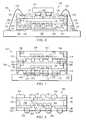
- FIG. 1illustrates electronic device 10 having a chip carrier substrate or printed circuit board (PCB) 12 with a plurality of semiconductor packages mounted on its surface.
- Electronic device 10may have one type of semiconductor package, or multiple types of semiconductor packages, depending on the application. The different types of semiconductor packages are shown in FIG. 1 for purposes of illustration.
- Electronic device 10may be a stand-alone system that uses the semiconductor packages to perform an electrical function.
- electronic device 10may be a subcomponent of a larger system.
- electronic device 10may be a graphics card, network interface card, or other signal processing card that can be inserted into a computer.
- the semiconductor packagecan include microprocessors, memories, application specific integrated circuits (ASICs), logic circuits, analog circuits, RF circuits, discrete devices, or other semiconductor die or electrical components.
- PCB 12provides a general substrate for structural support and electrical interconnect of the semiconductor packages mounted on the PCB.
- Conductive signal traces 14are formed on a surface or within layers of PCB 12 using evaporation, electrolytic plating, electroless plating, screen printing, PVD, or other suitable metal deposition process. Signal traces 14 provide for electrical communication between each of the semiconductor packages, mounted components, and other external system components. Traces 14 also provide power and ground connections to each of the semiconductor packages.
- a semiconductor devicehas two packaging levels.
- First level packagingis the technique for mechanically and electrically attaching the semiconductor die to a carrier.
- Second level packaginginvolves mechanically and electrically attaching the carrier to the PCB.
- a semiconductor devicemay only have the first level packaging where the die is mechanically and electrically mounted directly to the PCB.
- first level packagingincluding wire bond package 16 and flip chip 18
- second level packagingincluding ball grid array (BGA) 20 , bump chip carrier (BCC) 22 , dual in-line package (DIP) 24 , land grid array (LGA) 26 , multi-chip module (MCM) 28 , quad flat non-leaded package (QFN) 30 , and quad flat package 32 .
- BGAball grid array
- BCCbump chip carrier
- DIPdual in-line package
- LGAland grid array
- MCMmulti-chip module
- QFNquad flat non-leaded package
- quad flat package 32quad flat package
- electronic device 10includes a single attached semiconductor package, while other embodiments call for multiple interconnected packages.
- manufacturerscan incorporate pre-made components into electronic devices and systems. Because the semiconductor packages include sophisticated functionality, electronic devices can be manufactured using cheaper components and a shorter manufacturing process. The resulting devices are less likely to fail and less expensive to manufacture resulting in lower costs for consumers.
- FIG. 2 aillustrates further detail of DIP 24 mounted on PCB 12 .
- DIP 24includes semiconductor die 34 having contact pads 36 .
- Semiconductor die 34includes an active area containing analog or digital circuits implemented as active devices, passive devices, conductive layers, and dielectric layers formed within semiconductor die 34 and are electrically interconnected according to the electrical design of the die.
- the circuitmay include one or more transistors, diodes, inductors, capacitors, resistors, and other circuit elements formed within the active area of die 34 .
- Contact pads 36are made with a conductive material, such as aluminum (Al), copper (Cu), tin (Sn), nickel (Ni), gold (Au), or silver (Ag), and are electrically connected to the circuit elements formed within die 34 .
- Contact pads 36are formed by PVD, CVD, electrolytic plating, or electroless plating process.
- semiconductor die 34is mounted to a carrier 38 using a gold-silicon eutectic layer or adhesive material such as thermal epoxy.
- the package bodyincludes an insulative packaging material such as polymer or ceramic.
- Conductor leads 40are connected to carrier 38 and wire bonds 42 are formed between leads 40 and contact pads 36 of die 34 as a first level packaging.
- Encapsulant 44is deposited over the package for environmental protection by preventing moisture and particles from entering the package and contaminating die 34 , contact pads 36 , or wire bonds 42 .
- DIP 24is connected to PCB 12 by inserting leads 40 into holes formed through PCB 12 .
- Solder material 46is flowed around leads 40 and into the holes to physically and electrically connect DIP 24 to PCB 12 .
- Solder material 46can be any metal or electrically conductive material, e.g., Sn, lead (Pb), Au, Ag, Cu, zinc (Zn), bismuthinite (Bi), and alloys thereof, with an optional flux material.
- the solder materialcan be eutectic Sn/Pb, high-lead, or lead-free.
- FIG. 2 billustrates further detail of BCC 22 mounted on PCB 12 .
- Semiconductor die 16is connected to a carrier by wire bond style first level packaging.
- BCC 22is mounted to PCB 12 with a BCC style second level packaging.
- Semiconductor die 16 having contact pads 48is mounted over a carrier using an underfill or epoxy-resin adhesive material 50 .
- Semiconductor die 16includes an active area containing analog or digital circuits implemented as active devices, passive devices, conductive layers, and dielectric layers formed within semiconductor die 16 and are electrically interconnected according to the electrical design of the die.
- the circuitmay include one or more transistors, diodes, inductors, capacitors, resistors, and other circuit elements formed within the active area of die 16 .
- Contact pads 48are made with a conductive material, such as Al, Cu, Sn, Ni, Au, or Ag, and are electrically connected to the circuit elements formed within die 16 .
- Contact pads 48are formed by PVD, CVD, electrolytic plating, or electroless plating process.
- Wire bonds 54 and bond pads 56 and 58electrically connect contact pads 48 of semiconductor die 16 to contact pads 52 of BCC 22 forming the first level packaging.
- Molding compound or encapsulant 60is deposited over semiconductor die 16 , wire bonds 54 , contact pads 48 , and contact pads 52 to provide physical support and electrical isolation for the device.
- Contact pads 64are formed on a surface of PCB 12 using evaporation, electrolytic plating, electroless plating, screen printing, PVD, or other suitable metal deposition process and are typically plated to prevent oxidation. Contact pads 64 electrically connect to one or more conductive signal traces 14 . Solder material is deposited between contact pads 52 of BCC 22 and contact pads 64 of PCB 12 . The solder material is reflowed to form bumps 66 which form a mechanical and electrical connection between BCC 22 and PCB 12 .
- semiconductor die 18is mounted face down to carrier 76 with a flip chip style first level packaging.
- BGA 20is attached to PCB 12 with a BGA style second level packaging.
- Active area 70 containing analog or digital circuits implemented as active devices, passive devices, conductive layers, and dielectric layers formed within semiconductor die 18is electrically interconnected according to the electrical design of the die.
- the circuitmay include one or more transistors, diodes, inductors, capacitors, resistors, and other circuit elements formed within active area 70 of semiconductor die 18 .
- Semiconductor die 18is electrically and mechanically attached to carrier 76 through a large number of individual conductive solder bumps or balls 78 .
- Solder bumps 78are formed on bump pads or interconnect sites 80 , which are disposed on active areas 70 .
- Bump pads 80are made with a conductive material, such as Al, Cu, Sn, Ni, Au, or Ag, and are electrically connected to the circuit elements formed in active area 70 .
- Bump pads 80are formed by PVD, CVD, electrolytic plating, or electroless plating process.
- Solder bumps 78are electrically and mechanically connected to contact pads or interconnect sites 82 on carrier 76 by a solder reflow process.
- BGA 20is electrically and mechanically attached to PCB 12 by a large number of individual conductive solder bumps or balls 86 .
- the solder bumpsare formed on bump pads or interconnect sites 84 .
- the bump pads 84are electrically connected to interconnect sites 82 through conductive lines 90 routed through carrier 76 .
- Contact pads 88are formed on a surface of PCB 12 using evaporation, electrolytic plating, electroless plating, screen printing, PVD, or other suitable metal deposition process and are typically plated to prevent oxidation.
- Contact pads 88electrically connect to one or more conductive signal traces 14 .
- the solder bumps 86are electrically and mechanically connected to contact pads or bonding pads 88 on PCB 12 by a solder reflow process.
- Molding compound or encapsulant 92is deposited over semiconductor die 18 and carrier 76 to provide physical support and electrical isolation for the device.
- the flip chip semiconductor deviceprovides a short electrical conduction path from the active devices on semiconductor die 18 to conduction tracks on PCB 12 in order to reduce signal propagation distance, lower capacitance, and achieve overall better circuit performance.
- the semiconductor die 18can be mechanically and electrically attached directly to PCB 12 using flip chip style first level packaging without carrier 76 .
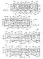
- FIGS. 3 a - 3 qillustrate a process of forming a stackable wafer level chip scale package (WLCSP) using an embedded wafer-shaped metal frame carrier.
- FIGS. 3 a - 3 bshow a top view and cross-sectional view of a temporary process carrier or substrate 100 with an adhesive layer 102 deposited on its surface.
- Carrier 100is a wafer-shaped dummy or sacrificial base material such as silicon, ceramic, glass, metal, or other suitable low-cost, rigid material.
- Adhesive layer 102can be a flexible plastic base film, such as polyvinyl chloride (PVC) or polyolefin, with a synthetic acrylic adhesive or ultraviolet (UV)-sensitive adhesive, for device mounting and removal.
- Adhesive layer 102is releasable by light, heat, laser, or mechanical pressure.
- an adhesive materialsuch as thermal epoxy, polymer composite, or inorganic bonding compounds, can be applied to carrier 100 .
- FIG. 3 ca metal frame carrier 104 is attached to adhesive layer 102 on carrier 100 .
- Metal frame carrier 104has a similar shape or form factor as carrier 100 .
- Metal frame carrier 104can be prefabricated using a leadframe manufacturing process to reduce manufacturing costs.
- FIG. 3 dis a cross-sectional view taken along line 3 d of metal frame carrier 104 on carrier 100 .
- Frame carrier 104includes a plurality of semiconductor die mounting sites 106 . Each mounting site 106 has a lead finger or leadframe interconnect structure 108 around cavity 110 .
- the lead finger interconnect structure 108includes a conductive post 111 with lead fingers 112 extending from the conductive post.
- Tie bars 113electrically connect conductive posts 111 between adjacent mounting sites 106 .
- Alignment marks 114such as grooves or plating lines, separate each mounting site 106 .
- Alignment marks 114are used to place semiconductor die 116 in cavity 110 with active surface facing adhesive layer 102 , as shown in top view of FIG. 3 e and cross-sectional view of FIG. 3 f .
- Semiconductor die 116are placed with active surface down to adhesive layer 102 .
- Alignment marks 114are optional. Other alignment methods can be used to place semiconductor die 116 in cavity 110 .
- Semiconductor die 116may contain analog or digital circuits implemented as active devices, integrated passive devices (IPD), conductive layers, signal traces, and dielectric layers.
- IPDsinclude inductors, capacitors, and resistors. These devices are electrically interconnected according to the electrical design and function of the die.
- an encapsulant or molding compound 118is deposited over and around semiconductor die 116 in cavity 110 using a screen printing, compressive molding, transfer molding, liquid encapsulant molding, liquid dispensing, or other suitable applicator.
- FIG. 3 his a cross-sectional view taken along line 3 h of encapsulant 118 formed in cavity 110 .
- Encapsulant 118can be epoxy resin, epoxy acrylate, polymer, or polymer composite material.
- Encapsulant 118is non-conductive and environmentally protects the semiconductor device from external elements and contaminants.
- encapsulant 118entirely covers metal frame carrier 104 , as shown in FIG. 3 i .
- Encapsulant 118is then planarized with grinder 120 to expose lead finger interconnect structure 108 , see FIG. 3 j.
- FIG. 3 kan electrically conductive layer 122 is patterned and deposited over lead finger interconnect structure 108 and encapsulant 118 .
- FIG. 3 lis a cross-sectional view taken along line 31 of conductive layer 122 formed over lead finger interconnect structure 108 and encapsulant 118 .
- Conductive layer 122can be Al, Cu, Sn, Ni, Au, Ag, or other suitable electrically conductive material.
- Conductive layer 122is formed by PVD, CVD, electrolytic plating, or electroless plating process. Conductive layer 122 electrically connects to lead finger interconnect structure 108 .
- an insulating layer 124is formed over conductive layer 122 and frame carrier 104 .
- the insulating layer 124can be polyimide (PI), benzocyclobutene (BCB), silicon dioxide (SiO2), silicon nitride (Si3N4), silicon oxynitride (SiON), tantalum pentoxide (Ta2O5), zircon (ZrO2), aluminum oxide (Al2O3), or other material having suitable insulating properties.
- the deposition of insulating layer 124may involve spin-coating, spray-coating, laminating, PVD, CVD, printing, sintering, or thermal oxidation.
- the insulating layer 124can single or multiple layers. A portion of insulating layer 124 is removed to expose conductive layer 122 .
- the temporary process carrier 100 and adhesive layer 102are removed in FIG. 3 n .
- the assemblyis inverted so that the active surfaces of semiconductor die 116 face upward.
- an interconnect build-up layer 126is formed to electrically connect semiconductor die 116 to external electrical components through lead finger interconnect structure 108 .
- the build-up layer 126includes electrically conductive layers 128 and 132 and conductive via 130 .
- Conductive layers 128 - 132can be Al, Cu, Sn, Ni, Au, Ag, or other suitable electrically conductive material.
- Conductive layers 128 - 132is formed by PVD, CVD, electrolytic plating, electroless plating, or other suitable metal deposition process.
- An insulating layer 134is formed around conductive layers 128 - 132 .
- the insulating layer 134can be PI, BCB, SiO2, Si3N4, SiON, Ta2O5, ZrO2, Al2O3, or other material having suitable insulating properties.
- the deposition of insulating layer 134may involve spin-coating, spray-coating, laminating, PVD, CVD, printing, sintering, or thermal oxidation.
- an electrically conductive solder materialis deposited over conductive layer 132 using an evaporation, electrolytic plating, electroless plating, ball drop, or screen printing process.
- the solder materialcan be any metal or electrically conductive material, e.g., Sn, Ni, Au, Ag, Pb, Bi, and alloys thereof, with an optional flux material.
- the solder materialcan be eutectic Sn/Pb, high lead, or lead free.
- the solder materialis reflowed by heating the material above its melting point to form spherical balls or bumps 136 . In some applications, solder bumps 136 are reflowed a second time to improve electrical contact to conductive layer 132 .
- Solder bumps 136represent one type of interconnect structure that can be formed on conductive layer 132 .
- lead finger interconnect structure 108is an integral part of the electrical interconnect between semiconductor die 116 and the external electric circuit components for the embedded die package.
- Semiconductor die 116electrically connects through conductive layers 128 - 132 and solder bumps 136 to external circuit components.
- Semiconductor die 116also electrically connects through conductive layers 128 - 132 , leadframe interconnect structure 108 , and conductive layer 122 to external circuit components.
- FIG. 3 qthe assembly from FIG. 3 p is placed on dicing tape 140 and singulated with saw blade or laser tool 142 into individual embedded semiconductor die packages 144 .
- FIG. 4shows one singulated embedded semiconductor die package 144 following the dicing operation.
- the encapsulant or molding compound 118is deposited over and around semiconductor die 116 .
- Conductive layer 122is patterned and deposited over encapsulant 118 .
- Conductive layer 122electrically connects to lead finger interconnect structure 108 .
- the insulating layer 124is formed over conductive layer 122 and encapsulant 118 .
- Conductive layers 128 - 132represent an interconnect build-up layer that electrically connects contact pads 127 on semiconductor die 116 to external electrical circuit components via solder bumps 136 .
- Conductive layer 122 and interconnect build-up layer 128 - 132may contain redistribution layer (RDL), one or more IPDs, thin-film circuit layer, contact pads, insulating layers, and signal traces.
- the insulating layer 134is formed around conductive layers 128 - 132 .
- FIG. 5illustrates vertically stacked embedded semiconductor die packages 144 - 146 , each made using the processing steps described in FIGS. 3 a - 3 q .
- Solder bumps 136 from embedded die package 144electrically connect to conductive layer 122 on embedded die package 146 made with conductive paste or solder material 148 .
- semiconductor die 116 in embedded die package 144is electrically connected to semiconductor die 116 in embedded die package 146 through conductive layer 122 , conductive layers 128 - 132 , solder bumps 136 , conductive paste 148 , and lead finger interconnect structure 108 of embedded die packages 144 and 146 .
- FIG. 6shows an embedded semiconductor die package 149 , similar to embedded die package 144 without solder bumps 136 .
- the embedded die package 149is mounted directly to substrate or printed circuit board (PCB) 150 using adhesive material 152 .
- Conductive layer 122 on embedded die package 149electrically connects to contact pads 153 on PCB 150 using wire bonds 154 .
- a semiconductor device or component 156is mounted to embedded die package 149 with solder bumps 158 .
- Semiconductor device 156contains discrete or integrated analog or digital circuits implemented as active devices, passive devices, conductive layers, and dielectric layers electrically interconnected according to the electrical design of the die.
- semiconductor die 116 in embedded die package 149 and semiconductor device 156are electrically connected together and to PCB 150 through conductive layer 122 , conductive layers 128 - 132 , solder bumps 158 , bond wires 154 , and lead finger interconnect structure 108 .
- vertically stacked embedded semiconductor die packages 160 - 162are each made using similar processing steps as described in FIGS. 3 a - 3 q , without backside conductive layer like 122 in FIG. 5 .
- Semiconductor die 164are disposed in a cavity surrounded by lead finger interconnect structure 166 and covered by encapsulant 168 .
- Conductive layer 170 and insulating layer 172are formed to electrically connect semiconductor die 164 to external electrical components.
- Semiconductor die 164 in embedded die package 160electrically connects to semiconductor die 164 in embedded die package 162 through conductive layer 170 , lead finger interconnect structure 166 , and solder bumps 174 .
- Semiconductor die 164 in embedded die packages 160 and 162further electrically connect through solder bumps 176 to contact pads 177 on PCB 178 .
- an embedded semiconductor die package 180is made using similar processing steps as described in FIGS. 3 a - 3 q , with a leadframe interconnect structure containing conductive posts but without lead fingers.
- Semiconductor die 182is disposed in a cavity surrounded by leadframe interconnect structure 184 and covered by encapsulant 188 .
- Conductive layer 192 and insulating layer 194are formed on a backside of embedded die package 180 to electrically connect semiconductor die 182 to external electrical components.
- conductive layer 198 and insulating layer 204are formed on an active side of embedded die package 180 to electrically connect semiconductor die 182 to external electrical components through solder bumps 206 .
- Leadframe interconnect structure 184includes a conductive post electrically connecting conductive layers 192 and 198 . Accordingly, semiconductor die 182 in embedded die package 180 is electrically connected to external circuit components through conductive layers 192 and 198 , leadframe interconnect structure 184 , and solder bumps 206 .
- an embedded semiconductor die package 210is made using similar processing steps as described in FIGS. 3 a - 3 q , with internal back-to-back, vertically stacked semiconductor die.
- Semiconductor die 212 and 214are bonded together with die attach adhesive film 216 and disposed in a cavity surrounded by lead finger interconnect structure 218 and covered by encapsulant 220 .
- Conductive layer 222 , conductive vias 224 , and insulating layer 226are formed on a backside of embedded die package 210 to electrically connect contact pads 228 of semiconductor die 214 to external electrical components.
- Conductive vias 224are formed by laser drilling insulating material 226 and encapsulant 220 and filling the void with conductive material or via plating.
- conductive layers 230 and 232 , conductive vias 234 , and insulating layer 236are formed on an active side of embedded die package 210 to electrically connect contact pads 238 of semiconductor die 212 to external electrical components through solder bumps 240 . Accordingly, semiconductor die 212 and 214 in embedded die package 210 are electrically connected to external circuit components through conductive layers 222 - 224 and 230 - 234 , leadframe interconnect structure 218 , and solder bumps 240 .
- an embedded semiconductor die package 250is made using similar processing steps as described in FIGS. 3 a - 3 q , with internal back-to-back, vertically stacked semiconductor die.
- Semiconductor die 252 and 254are bonded together with die attach adhesive film 256 and disposed in a cavity surrounded by lead finger interconnect structure 258 and covered by encapsulant 260 .
- Conductive layer 262 , conductive vias 264 , and insulating layer 266are formed on a backside of embedded die package 250 to electrically connect contact pads 268 of semiconductor die 254 to external electrical components.
- Conductive vias 264are formed by laser drilling insulating material 266 and filling the void with conductive material or via plating.
- conductive layers 270 and 272 , conductive vias 274 , and insulating layer 276are formed on an active side of embedded die package 250 to electrically connect contact pads 278 of semiconductor die 252 to external electrical components through solder bumps 280 .
- semiconductor die 252 and 254 in embedded die package 250are electrically connected to external circuit components through conductive layers 262 - 264 and 270 - 274 , leadframe interconnect structure 258 , and solder bumps 280 .
- FIG. 10further shows metal paste or solder interconnect structure 282 formed in encapsulant 260 to electrically connect conductive via 264 to contact pads 268 of semiconductor die 254 .
- an embedded semiconductor die package 290is made using similar processing steps as described in FIGS. 3 a - 3 q , with side-by-side internal semiconductor die.
- Semiconductor die 292 and 294are disposed side-by-side in a cavity surrounded by lead finger interconnect structure 296 and covered by encapsulant 298 .
- Conductive layer 302 , conductive via 301 , and insulating layer 304are formed on a first side of embedded die package 290 to electrically connect contact pads 306 of semiconductor die 292 to external electrical components.
- Conductive vias 301are formed by laser drilling encapsulant 298 and filling the void with conductive material or via plating.
- conductive layers 308 and insulating layer 310are formed on a second side of embedded die package 290 to electrically connect contact pads 312 of semiconductor die 294 to external electrical components through solder bumps 316 . Accordingly, semiconductor die 292 and 294 in embedded die package 290 are electrically connected to external circuit components through conductive layers 301 - 302 and 308 , leadframe interconnect structure 296 , and solder bumps 316 .
- an embedded semiconductor die package 320is made using similar processing steps as described in FIGS. 3 a - 3 q , with side-by-side internal semiconductor die.
- Semiconductor die 322 and 324are disposed side-by-side in a cavity surrounded by lead finger interconnect structure 326 and covered by encapsulant 328 .
- Conductive layer 332 and insulating layer 334are formed on a first side of embedded die package 320 to electrically connect contact pads 336 of semiconductor die 322 to external electrical components.
- a metal paste or solder interconnect structure 350is formed in encapsulant 328 to electrically connect conductive layer 332 to contact pads 336 of semiconductor die 322 .
- conductive layers 338 and insulating layer 340are formed on a second side of embedded die package 320 to electrically connect contact pads 342 of semiconductor die 324 to external electrical components through solder bumps 346 . Accordingly, semiconductor die 322 and 324 in embedded die package 320 are electrically connected to external circuit components through conductive layers 332 and 338 , leadframe interconnect structure 326 , and solder bumps 346 .
- a prefabricated frame carrieris bonded to a wafer-shaped temporary carrier which facilitates high density package assembly.
- the semiconductor dieare deposited in die mounting sites of the frame carrier and covered with encapsulant.
- Each die mounting siteincludes lead finger interconnect structure containing a conductive post and lead fingers extending from the conductive post to electrically connect to the embedded semiconductor die.
- the lead finger interconnect structureavoids the formation of conductive vias or z-interconnects as found in the prior art which reduces manufacturing costs.
- the semiconductor diecan be vertically stacked or placed side-by-side.
- the carrieris removed, followed by optional build-up interconnect structure and singulation into individual embedded die packages.
- the embedded die packagescan be vertically stacked with package interconnect structures.
- the lead finger interconnect structureis an integral part of the electrical interconnect, including the package interconnect structure, between the internal semiconductor die and the external electric circuit components for the embedded die package.
Landscapes
- Engineering & Computer Science (AREA)
- Microelectronics & Electronic Packaging (AREA)
- Computer Hardware Design (AREA)
- Power Engineering (AREA)
- Physics & Mathematics (AREA)
- Condensed Matter Physics & Semiconductors (AREA)
- General Physics & Mathematics (AREA)
- Manufacturing & Machinery (AREA)
- Structures Or Materials For Encapsulating Or Coating Semiconductor Devices Or Solid State Devices (AREA)
Abstract
Description
Claims (25)
Priority Applications (3)
| Application Number | Priority Date | Filing Date | Title |
|---|---|---|---|
| US12/912,467US8222717B2 (en) | 2008-07-14 | 2010-10-26 | Embedded semiconductor die package and method of making the same using metal frame carrier |
| US13/446,741US8659113B2 (en) | 2008-07-14 | 2012-04-13 | Embedded semiconductor die package and method of making the same using metal frame carrier |
| US14/154,049US9059186B2 (en) | 2008-07-14 | 2014-01-13 | Embedded semiconductor die package and method of making the same using metal frame carrier |
Applications Claiming Priority (3)
| Application Number | Priority Date | Filing Date | Title |
|---|---|---|---|
| US8053608P | 2008-07-14 | 2008-07-14 | |
| US12/266,313US7842542B2 (en) | 2008-07-14 | 2008-11-06 | Embedded semiconductor die package and method of making the same using metal frame carrier |
| US12/912,467US8222717B2 (en) | 2008-07-14 | 2010-10-26 | Embedded semiconductor die package and method of making the same using metal frame carrier |
Related Parent Applications (1)
| Application Number | Title | Priority Date | Filing Date |
|---|---|---|---|
| US12/266,313DivisionUS7842542B2 (en) | 2008-07-14 | 2008-11-06 | Embedded semiconductor die package and method of making the same using metal frame carrier |
Related Child Applications (1)
| Application Number | Title | Priority Date | Filing Date |
|---|---|---|---|
| US13/446,741ContinuationUS8659113B2 (en) | 2008-07-14 | 2012-04-13 | Embedded semiconductor die package and method of making the same using metal frame carrier |
Publications (2)
| Publication Number | Publication Date |
|---|---|
| US20110037154A1 US20110037154A1 (en) | 2011-02-17 |
| US8222717B2true US8222717B2 (en) | 2012-07-17 |
Family
ID=41504418
Family Applications (4)
| Application Number | Title | Priority Date | Filing Date |
|---|---|---|---|
| US12/266,313ActiveUS7842542B2 (en) | 2008-07-14 | 2008-11-06 | Embedded semiconductor die package and method of making the same using metal frame carrier |
| US12/912,467ActiveUS8222717B2 (en) | 2008-07-14 | 2010-10-26 | Embedded semiconductor die package and method of making the same using metal frame carrier |
| US13/446,741ActiveUS8659113B2 (en) | 2008-07-14 | 2012-04-13 | Embedded semiconductor die package and method of making the same using metal frame carrier |
| US14/154,049ActiveUS9059186B2 (en) | 2008-07-14 | 2014-01-13 | Embedded semiconductor die package and method of making the same using metal frame carrier |
Family Applications Before (1)
| Application Number | Title | Priority Date | Filing Date |
|---|---|---|---|
| US12/266,313ActiveUS7842542B2 (en) | 2008-07-14 | 2008-11-06 | Embedded semiconductor die package and method of making the same using metal frame carrier |
Family Applications After (2)
| Application Number | Title | Priority Date | Filing Date |
|---|---|---|---|
| US13/446,741ActiveUS8659113B2 (en) | 2008-07-14 | 2012-04-13 | Embedded semiconductor die package and method of making the same using metal frame carrier |
| US14/154,049ActiveUS9059186B2 (en) | 2008-07-14 | 2014-01-13 | Embedded semiconductor die package and method of making the same using metal frame carrier |
Country Status (1)
| Country | Link |
|---|---|
| US (4) | US7842542B2 (en) |
Cited By (2)
| Publication number | Priority date | Publication date | Assignee | Title |
|---|---|---|---|---|
| US20120199971A1 (en)* | 2008-07-14 | 2012-08-09 | Stats Chippac, Ltd. | Embedded Semiconductor Die Package and Method of Making the Same Using Metal Frame Carrier |
| EP2775523A1 (en) | 2013-03-04 | 2014-09-10 | Dialog Semiconductor GmbH | Chip on chip attach (passive IPD and PMIC) flip chip BGA using new cavity BGA substrate |
Families Citing this family (97)
| Publication number | Priority date | Publication date | Assignee | Title |
|---|---|---|---|---|
| TWI360207B (en)* | 2007-10-22 | 2012-03-11 | Advanced Semiconductor Eng | Chip package structure and method of manufacturing |
| TWI356479B (en)* | 2008-03-04 | 2012-01-11 | Advanced Semiconductor Eng | Package structure with embedded die and method of |
| US10026720B2 (en)* | 2015-05-20 | 2018-07-17 | Broadpak Corporation | Semiconductor structure and a method of making thereof |
| US8168470B2 (en) | 2008-12-08 | 2012-05-01 | Stats Chippac, Ltd. | Semiconductor device and method of forming vertical interconnect structure in substrate for IPD and baseband circuit separated by high-resistivity molding compound |
| US7858441B2 (en) | 2008-12-08 | 2010-12-28 | Stats Chippac, Ltd. | Semiconductor package with semiconductor core structure and method of forming same |
| US8097489B2 (en) | 2009-03-23 | 2012-01-17 | Stats Chippac, Ltd. | Semiconductor device and method of mounting pre-fabricated shielding frame over semiconductor die |
| US8378383B2 (en) | 2009-03-25 | 2013-02-19 | Stats Chippac, Ltd. | Semiconductor device and method of forming a shielding layer between stacked semiconductor die |
| US8003445B2 (en)* | 2009-03-26 | 2011-08-23 | Stats Chippac Ltd. | Integrated circuit packaging system with z-interconnects having traces and method of manufacture thereof |
| JP2010245107A (en)* | 2009-04-01 | 2010-10-28 | Shinko Electric Ind Co Ltd | Semiconductor device and manufacturing method thereof |
| TWI456715B (en)* | 2009-06-19 | 2014-10-11 | Advanced Semiconductor Eng | Chip package structure and manufacturing method thereof |
| TWI466259B (en)* | 2009-07-21 | 2014-12-21 | Advanced Semiconductor Eng | Semiconductor package, manufacturing method thereof and manufacturing method for chip-redistribution encapsulant |
| TWI405306B (en)* | 2009-07-23 | 2013-08-11 | Advanced Semiconductor Eng | Semiconductor package, manufacturing method thereof and chip-redistribution encapsulant |
| US8084853B2 (en)* | 2009-09-25 | 2011-12-27 | Mediatek Inc. | Semiconductor flip chip package utilizing wire bonding for net switching |
| US20110084372A1 (en) | 2009-10-14 | 2011-04-14 | Advanced Semiconductor Engineering, Inc. | Package carrier, semiconductor package, and process for fabricating same |
| US8378466B2 (en)* | 2009-11-19 | 2013-02-19 | Advanced Semiconductor Engineering, Inc. | Wafer-level semiconductor device packages with electromagnetic interference shielding |
| TWI497679B (en)* | 2009-11-27 | 2015-08-21 | Advanced Semiconductor Eng | Semiconductor package and manufacturing method thereof |
| US8569894B2 (en)* | 2010-01-13 | 2013-10-29 | Advanced Semiconductor Engineering, Inc. | Semiconductor package with single sided substrate design and manufacturing methods thereof |
| US8372689B2 (en)* | 2010-01-21 | 2013-02-12 | Advanced Semiconductor Engineering, Inc. | Wafer-level semiconductor device packages with three-dimensional fan-out and manufacturing methods thereof |
| US8320134B2 (en)* | 2010-02-05 | 2012-11-27 | Advanced Semiconductor Engineering, Inc. | Embedded component substrate and manufacturing methods thereof |
| US8183579B2 (en)* | 2010-03-02 | 2012-05-22 | Taiwan Semiconductor Manufacturing Company, Ltd. | LED flip-chip package structure with dummy bumps |
| TWI411075B (en)* | 2010-03-22 | 2013-10-01 | Advanced Semiconductor Eng | Semiconductor package and manufacturing method thereof |
| US8624374B2 (en) | 2010-04-02 | 2014-01-07 | Advanced Semiconductor Engineering, Inc. | Semiconductor device packages with fan-out and with connecting elements for stacking and manufacturing methods thereof |
| US8278746B2 (en) | 2010-04-02 | 2012-10-02 | Advanced Semiconductor Engineering, Inc. | Semiconductor device packages including connecting elements |
| US8357564B2 (en) | 2010-05-17 | 2013-01-22 | Stats Chippac, Ltd. | Semiconductor device and method of forming prefabricated multi-die leadframe for electrical interconnect of stacked semiconductor die |
| KR101665302B1 (en)* | 2010-05-20 | 2016-10-24 | 에베 그룹 에. 탈너 게엠베하 | Method for producing chip stacks, and a carrier for carrying out the method |
| US8318541B2 (en) | 2010-08-10 | 2012-11-27 | Stats Chippac, Ltd. | Semiconductor device and method of forming vertical interconnect in FO-WLCSP using leadframe disposed between semiconductor die |
| US8518746B2 (en)* | 2010-09-02 | 2013-08-27 | Stats Chippac, Ltd. | Semiconductor device and method of forming TSV semiconductor wafer with embedded semiconductor die |
| US8941222B2 (en) | 2010-11-11 | 2015-01-27 | Advanced Semiconductor Engineering Inc. | Wafer level semiconductor package and manufacturing methods thereof |
| US9406658B2 (en) | 2010-12-17 | 2016-08-02 | Advanced Semiconductor Engineering, Inc. | Embedded component device and manufacturing methods thereof |
| TWI462201B (en)* | 2011-03-04 | 2014-11-21 | Adl Engineering Inc | Semiconductor package structure and method for fabricating the same |
| TWI451543B (en)* | 2011-03-07 | 2014-09-01 | Unimicron Technology Corp | Package structure and its manufacturing method and package stacking device |
| US8836120B2 (en)* | 2011-04-19 | 2014-09-16 | Infineon Technologies Ag | Semiconductor device with a layer including niobium, and/or tantalum overlying a contact pad or a metal layer |
| US8288209B1 (en)* | 2011-06-03 | 2012-10-16 | Stats Chippac, Ltd. | Semiconductor device and method of using leadframe bodies to form openings through encapsulant for vertical interconnect of semiconductor die |
| JP6289364B2 (en)* | 2011-06-30 | 2018-03-07 | ムラタ エレクトロニクス オサケユキチュア | Method for manufacturing system-in-package device and system-in-package device |
| US9178093B2 (en) | 2011-07-06 | 2015-11-03 | Flextronics Ap, Llc | Solar cell module on molded lead-frame and method of manufacture |
| US8916421B2 (en)* | 2011-08-31 | 2014-12-23 | Freescale Semiconductor, Inc. | Semiconductor device packaging having pre-encapsulation through via formation using lead frames with attached signal conduits |
| US9142502B2 (en)* | 2011-08-31 | 2015-09-22 | Zhiwei Gong | Semiconductor device packaging having pre-encapsulation through via formation using drop-in signal conduits |
| US9236278B2 (en) | 2011-09-23 | 2016-01-12 | Stats Chippac Ltd. | Integrated circuit packaging system with a substrate embedded dummy-die paddle and method of manufacture thereof |
| US8597983B2 (en) | 2011-11-18 | 2013-12-03 | Freescale Semiconductor, Inc. | Semiconductor device packaging having substrate with pre-encapsulation through via formation |
| US8809996B2 (en) | 2012-06-29 | 2014-08-19 | Taiwan Semiconductor Manufacturing Company, Ltd. | Package with passive devices and method of forming the same |
| US9559039B2 (en) | 2012-09-17 | 2017-01-31 | STATS ChipPAC Pte. Ltd. | Semiconductor device and method of using substrate having base and conductive posts to form vertical interconnect structure in embedded die package |
| US9368460B2 (en)* | 2013-03-15 | 2016-06-14 | Taiwan Semiconductor Manufacturing Company, Ltd. | Fan-out interconnect structure and method for forming same |
| CN203279336U (en)* | 2013-04-27 | 2013-11-06 | 中兴通讯股份有限公司 | Inner heat dissipation terminal |
| US9530752B2 (en)* | 2013-11-11 | 2016-12-27 | Infineon Technologies Ag | Method for forming electronic components |
| US20150206855A1 (en)* | 2014-01-22 | 2015-07-23 | Mediatek Inc. | Semiconductor package |
| US9922844B2 (en) | 2014-03-12 | 2018-03-20 | Mediatek Inc. | Semiconductor package and method for fabricating base for semiconductor package |
| US20150279824A1 (en)* | 2014-03-28 | 2015-10-01 | Vijay K. Nair | Electronic package and method of forming an electronic package |
| US9691726B2 (en)* | 2014-07-08 | 2017-06-27 | Taiwan Semiconductor Manufacturing Company, Ltd. | Methods for forming fan-out package structure |
| TWI584387B (en)* | 2014-08-15 | 2017-05-21 | 矽品精密工業股份有限公司 | Method of manufacturing package structure |
| WO2016043761A1 (en) | 2014-09-18 | 2016-03-24 | Intel Corporation | Method of embedding wlcsp components in e-wlb and e-plb |
| US20180261535A1 (en)* | 2014-12-15 | 2018-09-13 | Bridge Semiconductor Corp. | Method of making wiring board with dual routing circuitries integrated with leadframe |
| TWI581690B (en)* | 2014-12-30 | 2017-05-01 | 恆勁科技股份有限公司 | Package apparatus and manufacturing method thereof |
| US9627311B2 (en) | 2015-01-22 | 2017-04-18 | Mediatek Inc. | Chip package, package substrate and manufacturing method thereof |
| DE102015104956A1 (en)* | 2015-03-31 | 2016-10-06 | Infineon Technologies Ag | Printed circuit board with a lead frame with inserted packaged semiconductor chips |
| US9837484B2 (en)* | 2015-05-27 | 2017-12-05 | STATS ChipPAC Pte. Ltd. | Semiconductor device and method of forming substrate including embedded component with symmetrical structure |
| US9443830B1 (en)* | 2015-06-09 | 2016-09-13 | Apple Inc. | Printed circuits with embedded semiconductor dies |
| US9455539B1 (en) | 2015-06-26 | 2016-09-27 | Apple Inc. | Connector having printed circuit with embedded die |
| DE102016102155B4 (en)* | 2016-02-08 | 2025-02-06 | Infineon Technologies Ag | A process for electroplating supported by a current distribution layer |
| US11211305B2 (en) | 2016-04-01 | 2021-12-28 | Texas Instruments Incorporated | Apparatus and method to support thermal management of semiconductor-based components |
| US20170309549A1 (en)* | 2016-04-21 | 2017-10-26 | Texas Instruments Incorporated | Sintered Metal Flip Chip Joints |
| CN109075151B (en) | 2016-04-26 | 2023-06-27 | 亚德诺半导体国际无限责任公司 | Lead frame for mechanical mating, and electrical and thermal conduction of component package circuits |
| US10861796B2 (en) | 2016-05-10 | 2020-12-08 | Texas Instruments Incorporated | Floating die package |
| US9892999B2 (en)* | 2016-06-07 | 2018-02-13 | Globalfoundries Inc. | Producing wafer level packaging using leadframe strip and related device |
| KR101973430B1 (en)* | 2016-09-19 | 2019-04-29 | 삼성전기주식회사 | Fan-out semiconductor package |
| US10085097B2 (en) | 2016-10-04 | 2018-09-25 | Starkey Laboratories, Inc. | Hearing assistance device incorporating system in package module |
| US9966341B1 (en) | 2016-10-31 | 2018-05-08 | Infineon Technologies Americas Corp. | Input/output pins for chip-embedded substrate |
| US10636768B2 (en) | 2016-11-01 | 2020-04-28 | Starkey Laboratories, Inc. | Integrated circuit module and method of forming same |
| US10179730B2 (en) | 2016-12-08 | 2019-01-15 | Texas Instruments Incorporated | Electronic sensors with sensor die in package structure cavity |
| US9761543B1 (en) | 2016-12-20 | 2017-09-12 | Texas Instruments Incorporated | Integrated circuits with thermal isolation and temperature regulation |
| US10074639B2 (en) | 2016-12-30 | 2018-09-11 | Texas Instruments Incorporated | Isolator integrated circuits with package structure cavity and fabrication methods |
| US9865537B1 (en) | 2016-12-30 | 2018-01-09 | Texas Instruments Incorporated | Methods and apparatus for integrated circuit failsafe fuse package with arc arrest |
| US10411150B2 (en) | 2016-12-30 | 2019-09-10 | Texas Instruments Incorporated | Optical isolation systems and circuits and photon detectors with extended lateral P-N junctions |
| US9929110B1 (en) | 2016-12-30 | 2018-03-27 | Texas Instruments Incorporated | Integrated circuit wave device and method |
| DE102017105017A1 (en)* | 2017-03-09 | 2018-09-13 | Osram Opto Semiconductors Gmbh | PREPARATION OF RADIATION-EMITTING COMPONENTS |
| US10121847B2 (en) | 2017-03-17 | 2018-11-06 | Texas Instruments Incorporated | Galvanic isolation device |
| US12283555B2 (en) | 2018-03-23 | 2025-04-22 | Analog Devices International Unlimited Company | Semiconductor packages |
| US10497635B2 (en) | 2018-03-27 | 2019-12-03 | Linear Technology Holding Llc | Stacked circuit package with molded base having laser drilled openings for upper package |
| US10727161B2 (en) | 2018-08-06 | 2020-07-28 | Texas Instruments Incorporated | Thermal and stress isolation for precision circuit |
| US11410977B2 (en) | 2018-11-13 | 2022-08-09 | Analog Devices International Unlimited Company | Electronic module for high power applications |
| US11342256B2 (en) | 2019-01-24 | 2022-05-24 | Applied Materials, Inc. | Method of fine redistribution interconnect formation for advanced packaging applications |
| TWI689052B (en)* | 2019-03-15 | 2020-03-21 | 鴻海精密工業股份有限公司 | Semiconductor package structure and method of manufacturing the same |
| IT201900006740A1 (en)* | 2019-05-10 | 2020-11-10 | Applied Materials Inc | SUBSTRATE STRUCTURING PROCEDURES |
| IT201900006736A1 (en) | 2019-05-10 | 2020-11-10 | Applied Materials Inc | PACKAGE MANUFACTURING PROCEDURES |
| US11931855B2 (en) | 2019-06-17 | 2024-03-19 | Applied Materials, Inc. | Planarization methods for packaging substrates |
| US11239168B2 (en)* | 2019-07-30 | 2022-02-01 | Industrial Technology Research Institute | Chip package structure |
| US11393774B2 (en)* | 2019-08-21 | 2022-07-19 | Stmicroelectronics, Inc. | Semiconductor device having cavities at an interface of an encapsulant and a die pad or leads |
| US11862546B2 (en) | 2019-11-27 | 2024-01-02 | Applied Materials, Inc. | Package core assembly and fabrication methods |
| US11257790B2 (en) | 2020-03-10 | 2022-02-22 | Applied Materials, Inc. | High connectivity device stacking |
| US11454884B2 (en) | 2020-04-15 | 2022-09-27 | Applied Materials, Inc. | Fluoropolymer stamp fabrication method |
| US11400545B2 (en) | 2020-05-11 | 2022-08-02 | Applied Materials, Inc. | Laser ablation for package fabrication |
| US11844178B2 (en) | 2020-06-02 | 2023-12-12 | Analog Devices International Unlimited Company | Electronic component |
| US11232951B1 (en) | 2020-07-14 | 2022-01-25 | Applied Materials, Inc. | Method and apparatus for laser drilling blind vias |
| US11676832B2 (en) | 2020-07-24 | 2023-06-13 | Applied Materials, Inc. | Laser ablation system for package fabrication |
| US11521937B2 (en) | 2020-11-16 | 2022-12-06 | Applied Materials, Inc. | Package structures with built-in EMI shielding |
| US11404318B2 (en) | 2020-11-20 | 2022-08-02 | Applied Materials, Inc. | Methods of forming through-silicon vias in substrates for advanced packaging |
| US11705365B2 (en) | 2021-05-18 | 2023-07-18 | Applied Materials, Inc. | Methods of micro-via formation for advanced packaging |
| US12183684B2 (en) | 2021-10-26 | 2024-12-31 | Applied Materials, Inc. | Semiconductor device packaging methods |
Citations (10)
| Publication number | Priority date | Publication date | Assignee | Title |
|---|---|---|---|---|
| US5250843A (en) | 1991-03-27 | 1993-10-05 | Integrated System Assemblies Corp. | Multichip integrated circuit modules |
| US5353498A (en) | 1993-02-08 | 1994-10-11 | General Electric Company | Method for fabricating an integrated circuit module |
| US5792676A (en)* | 1995-10-03 | 1998-08-11 | Mitsubishi Denki Kabushiki Kaisha | Method of fabricating power semiconductor device and lead frame |
| US5822190A (en)* | 1996-06-11 | 1998-10-13 | Kabushiki Kaisha Toshiba | Card type memory device and a method for manufacturing the same |
| US5841193A (en) | 1996-05-20 | 1998-11-24 | Epic Technologies, Inc. | Single chip modules, repairable multichip modules, and methods of fabrication thereof |
| US6414396B1 (en)* | 2000-01-24 | 2002-07-02 | Amkor Technology, Inc. | Package for stacked integrated circuits |
| US6717822B1 (en)* | 2002-09-20 | 2004-04-06 | Amkor Technology, Inc. | Lead-frame method and circuit module assembly including edge stiffener |
| US7439100B2 (en) | 2005-08-18 | 2008-10-21 | Semiconductor Components Industries, L.L.C. | Encapsulated chip scale package having flip-chip on lead frame structure and method |
| US7598600B2 (en) | 2005-03-30 | 2009-10-06 | Stats Chippac Ltd. | Stackable power semiconductor package system |
| US7619901B2 (en) | 2007-06-25 | 2009-11-17 | Epic Technologies, Inc. | Integrated structures and fabrication methods thereof implementing a cell phone or other electronic system |
Family Cites Families (4)
| Publication number | Priority date | Publication date | Assignee | Title |
|---|---|---|---|---|
| US6313522B1 (en)* | 1998-08-28 | 2001-11-06 | Micron Technology, Inc. | Semiconductor structure having stacked semiconductor devices |
| US8178982B2 (en) | 2006-12-30 | 2012-05-15 | Stats Chippac Ltd. | Dual molded multi-chip package system |
| US7842542B2 (en)* | 2008-07-14 | 2010-11-30 | Stats Chippac, Ltd. | Embedded semiconductor die package and method of making the same using metal frame carrier |
| US7993941B2 (en)* | 2008-12-05 | 2011-08-09 | Stats Chippac, Ltd. | Semiconductor package and method of forming Z-direction conductive posts embedded in structurally protective encapsulant |
- 2008
- 2008-11-06USUS12/266,313patent/US7842542B2/enactiveActive
- 2010
- 2010-10-26USUS12/912,467patent/US8222717B2/enactiveActive
- 2012
- 2012-04-13USUS13/446,741patent/US8659113B2/enactiveActive
- 2014
- 2014-01-13USUS14/154,049patent/US9059186B2/enactiveActive
Patent Citations (10)
| Publication number | Priority date | Publication date | Assignee | Title |
|---|---|---|---|---|
| US5250843A (en) | 1991-03-27 | 1993-10-05 | Integrated System Assemblies Corp. | Multichip integrated circuit modules |
| US5353498A (en) | 1993-02-08 | 1994-10-11 | General Electric Company | Method for fabricating an integrated circuit module |
| US5792676A (en)* | 1995-10-03 | 1998-08-11 | Mitsubishi Denki Kabushiki Kaisha | Method of fabricating power semiconductor device and lead frame |
| US5841193A (en) | 1996-05-20 | 1998-11-24 | Epic Technologies, Inc. | Single chip modules, repairable multichip modules, and methods of fabrication thereof |
| US5822190A (en)* | 1996-06-11 | 1998-10-13 | Kabushiki Kaisha Toshiba | Card type memory device and a method for manufacturing the same |
| US6414396B1 (en)* | 2000-01-24 | 2002-07-02 | Amkor Technology, Inc. | Package for stacked integrated circuits |
| US6717822B1 (en)* | 2002-09-20 | 2004-04-06 | Amkor Technology, Inc. | Lead-frame method and circuit module assembly including edge stiffener |
| US7598600B2 (en) | 2005-03-30 | 2009-10-06 | Stats Chippac Ltd. | Stackable power semiconductor package system |
| US7439100B2 (en) | 2005-08-18 | 2008-10-21 | Semiconductor Components Industries, L.L.C. | Encapsulated chip scale package having flip-chip on lead frame structure and method |
| US7619901B2 (en) | 2007-06-25 | 2009-11-17 | Epic Technologies, Inc. | Integrated structures and fabrication methods thereof implementing a cell phone or other electronic system |
Cited By (6)
| Publication number | Priority date | Publication date | Assignee | Title |
|---|---|---|---|---|
| US20120199971A1 (en)* | 2008-07-14 | 2012-08-09 | Stats Chippac, Ltd. | Embedded Semiconductor Die Package and Method of Making the Same Using Metal Frame Carrier |
| US8659113B2 (en)* | 2008-07-14 | 2014-02-25 | Stats Chippac, Ltd. | Embedded semiconductor die package and method of making the same using metal frame carrier |
| US9059186B2 (en) | 2008-07-14 | 2015-06-16 | Stats Chippac, Ltd. | Embedded semiconductor die package and method of making the same using metal frame carrier |
| EP2775523A1 (en) | 2013-03-04 | 2014-09-10 | Dialog Semiconductor GmbH | Chip on chip attach (passive IPD and PMIC) flip chip BGA using new cavity BGA substrate |
| EP3133645A1 (en) | 2013-03-04 | 2017-02-22 | Dialog Semiconductor GmbH | Chip on chip attach (passive ipd and pmic) flip chip bga using new cavity bga substrate |
| US9929130B2 (en) | 2013-03-04 | 2018-03-27 | Dialog Semiconductor Gmbh | Chip on chip attach (passive IPD and PMIC) flip chip BGA using new cavity BGA substrate |
Also Published As
| Publication number | Publication date |
|---|---|
| US20140127858A1 (en) | 2014-05-08 |
| US7842542B2 (en) | 2010-11-30 |
| US20120199971A1 (en) | 2012-08-09 |
| US9059186B2 (en) | 2015-06-16 |
| US8659113B2 (en) | 2014-02-25 |
| US20110037154A1 (en) | 2011-02-17 |
| US20100006994A1 (en) | 2010-01-14 |
Similar Documents
| Publication | Publication Date | Title |
|---|---|---|
| US9059186B2 (en) | Embedded semiconductor die package and method of making the same using metal frame carrier | |
| US9478486B2 (en) | Semiconductor device and method of forming topside and bottom-side interconnect structures around core die with TSV | |
| US8357564B2 (en) | Semiconductor device and method of forming prefabricated multi-die leadframe for electrical interconnect of stacked semiconductor die | |
| US9099455B2 (en) | Semiconductor device and method of forming conductive posts embedded in photosensitive encapsulant | |
| US9966335B2 (en) | Semiconductor device and method of forming interposer frame electrically connected to embedded semiconductor die | |
| US10141222B2 (en) | Semiconductor device and method of forming conductive vias through interconnect structures and encapsulant of WLCSP | |
| US8466544B2 (en) | Semiconductor device and method of forming interposer and opposing build-up interconnect structure with connecting conductive TMV for electrical interconnect of Fo-WLCSP | |
| US8895440B2 (en) | Semiconductor die and method of forming Fo-WLCSP vertical interconnect using TSV and TMV | |
| US9431331B2 (en) | Semiconductor device and method of forming penetrable film encapsulant around semiconductor die and interconnect structure | |
| US9515016B2 (en) | Semiconductor package and method of forming z-direction conductive posts embedded in structurally protective encapsulant | |
| US8076184B1 (en) | Semiconductor device and method of forming wafer-level multi-row etched leadframe with base leads and embedded semiconductor die | |
| US8518746B2 (en) | Semiconductor device and method of forming TSV semiconductor wafer with embedded semiconductor die | |
| US8283250B2 (en) | Semiconductor device and method of forming a conductive via-in-via structure | |
| US8137995B2 (en) | Double-sided semiconductor device and method of forming top-side and bottom-side interconnect structures |
Legal Events
| Date | Code | Title | Description |
|---|---|---|---|
| STCF | Information on status: patent grant | Free format text:PATENTED CASE | |
| CC | Certificate of correction | ||
| AS | Assignment | Owner name:CITICORP INTERNATIONAL LIMITED, AS COMMON SECURITY AGENT, HONG KONG Free format text:SECURITY INTEREST;ASSIGNORS:STATS CHIPPAC, INC.;STATS CHIPPAC LTD.;REEL/FRAME:036288/0748 Effective date:20150806 Owner name:CITICORP INTERNATIONAL LIMITED, AS COMMON SECURITY Free format text:SECURITY INTEREST;ASSIGNORS:STATS CHIPPAC, INC.;STATS CHIPPAC LTD.;REEL/FRAME:036288/0748 Effective date:20150806 | |
| FPAY | Fee payment | Year of fee payment:4 | |
| AS | Assignment | Owner name:STATS CHIPPAC PTE. LTE., SLOVENIA Free format text:CHANGE OF NAME;ASSIGNOR:STATS CHIPPAC LTD.;REEL/FRAME:038378/0352 Effective date:20160329 | |
| AS | Assignment | Owner name:STATS CHIPPAC PTE. LTE., SINGAPORE Free format text:CHANGE OF NAME;ASSIGNOR:STATS CHIPPAC LTD.;REEL/FRAME:038388/0036 Effective date:20160329 | |
| MAFP | Maintenance fee payment | Free format text:PAYMENT OF MAINTENANCE FEE, 8TH YEAR, LARGE ENTITY (ORIGINAL EVENT CODE: M1552); ENTITY STATUS OF PATENT OWNER: LARGE ENTITY Year of fee payment:8 | |
| AS | Assignment | Owner name:STATS CHIPPAC, INC., CALIFORNIA Free format text:RELEASE BY SECURED PARTY;ASSIGNOR:CITICORP INTERNATIONAL LIMITED, AS COMMON SECURITY AGENT;REEL/FRAME:052864/0057 Effective date:20190503 Owner name:STATS CHIPPAC PTE. LTD. FORMERLY KNOWN AS STATS CHIPPAC LTD., SINGAPORE Free format text:RELEASE BY SECURED PARTY;ASSIGNOR:CITICORP INTERNATIONAL LIMITED, AS COMMON SECURITY AGENT;REEL/FRAME:052864/0057 Effective date:20190503 | |
| AS | Assignment | Owner name:STATS CHIPPAC PTE. LTE., SINGAPORE Free format text:CORRECT ERROR IN ASSIGNMENT NAME FROM STATS CHIPPAC PTE. LTE. TO STATS CHIPPAC PTE. LTD. (REEL: 38388 FRAME: 0036;ASSIGNOR:STATS CHIPPAC LTD.;REEL/FRAME:064789/0885 Effective date:20160329 | |
| AS | Assignment | Owner name:STATS CHIPPAC PTE. LTD., SINGAPORE Free format text:CORRECTIVE ASSIGNMENT TO CORRECT A TYPOGRAPHICAL ERROR ON THE COVER SHEET PREVIOUSLY RECORDED AT REEL: 038388 FRAME: 0036. ASSIGNOR(S) HEREBY CONFIRMS THE CHANGE OF NAME;ASSIGNOR:STATS CHIPPAC LTD.;REEL/FRAME:064834/0911 Effective date:20160329 Owner name:STATS CHIPPAC PTE. LTD., SINGAPORE Free format text:CORRECTIVE ASSIGNMENT TO CORRECT A TYPOGRAPHICAL ERROR ON THE COVER SHEET PREVIOUSLY RECORDED AT REEL: 064789 FRAME: 0885. ASSIGNOR(S) HEREBY CONFIRMS THE CORRECTIVE ASSIGNMENT;ASSIGNOR:STATS CHIPPAC LTD.;REEL/FRAME:064836/0363 Effective date:20160329 | |
| MAFP | Maintenance fee payment | Free format text:PAYMENT OF MAINTENANCE FEE, 12TH YEAR, LARGE ENTITY (ORIGINAL EVENT CODE: M1553); ENTITY STATUS OF PATENT OWNER: LARGE ENTITY Year of fee payment:12 |